ICGOO在线商城 > 集成电路(IC) > PMIC - 稳压器 - 线性 > TPS78001DRVR
 Datasheet下载
- 型号: TPS78001DRVR
- 制造商: Texas Instruments
- 库位|库存: xxxx|xxxx
- 要求:
| 数量阶梯 | 香港交货 | 国内含税 |
| +xxxx | $xxxx | ¥xxxx |
查看当月历史价格
查看今年历史价格
TPS78001DRVR产品简介:
ICGOO电子元器件商城为您提供TPS78001DRVR由Texas Instruments设计生产,在icgoo商城现货销售,并且可以通过原厂、代理商等渠道进行代购。 TPS78001DRVR价格参考。Texas InstrumentsTPS78001DRVR封装/规格:PMIC - 稳压器 - 线性, Linear Voltage Regulator IC Positive Adjustable 1 Output 1.22 V ~ 5.25 V 150mA 6-SON (2x2)。您可以下载TPS78001DRVR参考资料、Datasheet数据手册功能说明书,资料中有TPS78001DRVR 详细功能的应用电路图电压和使用方法及教程。
TPS78001DRVR 是 Texas Instruments(德州仪器)推出的一款 PMIC - 稳压器 - 线性产品,属于低功耗、低压降线性稳压器(LDO)。其主要应用场景如下:

 1. 便携式电子设备
   - TPS78001DRVR 的低静态电流(典型值为 65 µA)和小封装尺寸(如 SOT-23 或 VSSOP),使其非常适合用于电池供电的便携式设备。
   - 应用实例:智能手机、平板电脑、可穿戴设备(如智能手表和健康追踪器)、蓝牙耳机等。

 2. 物联网 (IoT) 设备
   - 在 IoT 领域,该器件的高效能和低功耗特性能够延长电池寿命,适用于各种传感器节点、无线模块和智能家居设备。
   - 应用实例:环境监测传感器、智能家居控制器、无线通信模块(如 Zigbee、LoRa 和 Wi-Fi 模块)。

 3. 工业自动化
   - 由于其高精度输出电压调节能力(±1% 精度)和良好的瞬态响应,TPS78001DRVR 可用于工业自动化中的低功耗控制单元。
   - 应用实例:数据采集系统、远程监控设备、工业传感器接口。

 4. 医疗电子
   - 在医疗领域,该器件的小尺寸和低噪声性能适合对空间和信号质量有严格要求的应用。
   - 应用实例:便携式医疗设备(如血糖仪、脉搏血氧仪)、助听器和其他低功耗医疗监测装置。

 5. 消费类电子产品
   - 其简单的设计和易于使用的特性使得 TPS78001DRVR 成为消费类电子产品的理想选择。
   - 应用实例:数码相机、游戏控制器、遥控器和其他小型电子设备。

 特性总结
- 输入电压范围:1.7V 至 5.5V
- 输出电压范围:0.8V 至 3.3V(固定版本)或可调版本
- 最大输出电流:150mA
- 低 dropout 电压:200mV(在 150mA 下)
- 内置过流保护和热关断功能

这些特性使其成为需要稳定电源供应且对功耗敏感的应用的理想选择。
| 参数 | 数值 |
| 产品目录 | 集成电路 (IC)半导体 |
| 描述 | IC REG LDO ADJ 0.15A 6SON低压差稳压器 Sgl Output LDO 150mA Adj |
| 产品分类 | |
| 品牌 | Texas Instruments |
| 产品手册 | http://www.ti.com/lit/gpn/tps78001 |
| 产品图片 |
|
| rohs | 符合RoHS无铅 / 符合限制有害物质指令(RoHS)规范要求 |
| 产品系列 | 电源管理 IC,低压差稳压器,Texas Instruments TPS78001DRVR- |
| 数据手册 | |
| 产品型号 | TPS78001DRVR |
| 产品目录页面 | |
| 产品种类 | 低压差稳压器 |
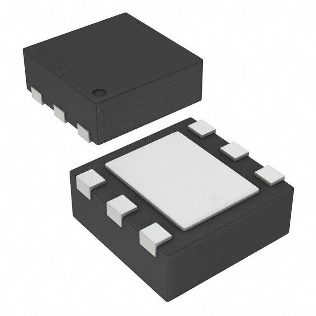
| 供应商器件封装 | 6-SON(2x2) |
| 其它名称 | 296-23438-1 |
| 制造商产品页 | http://www.ti.com/general/docs/suppproductinfo.tsp?distId=10&orderablePartNumber=TPS78001DRVR |
| 包装 | 剪切带 (CT) |
| 单位重量 | 9.700 mg |
| 参考电压 | 1.216 V |
| 商标 | Texas Instruments |
| 回动电压—最大值 | 250 mV |
| 安装类型 | 表面贴装 |
| 安装风格 | SMD/SMT |
| 封装 | Reel |
| 封装/外壳 | 6-WDFN 裸露焊盘 |
| 封装/箱体 | WSON-6 |
| 工作温度 | -40°C ~ 125°C |
| 工厂包装数量 | 3000 |
| 最大功率耗散 | 1.54 W |
| 最大工作温度 | + 125 C |
| 最大输入电压 | 5.5 V |
| 最小工作温度 | - 40 C |
| 最小输入电压 | + 2.2 V |
| 标准包装 | 1 |
| 电压-跌落(典型值) | - |
| 电压-输入 | 2.2 V ~ 5.5 V |
| 电压-输出 | 1.22 V ~ 5.25 V |
| 电压调节准确度 | 2 % |
| 电流-输出 | 150mA |
| 电流-限制(最小值) | 150mA |
| 稳压器拓扑 | 正,可调式 |
| 稳压器数 | 1 |
| 系列 | TPS78001 |
| 线路调整率 | 1 % |
| 负载调节 | 2 % |
| 输出电压 | 1.22 V to 5.25 V |
| 输出电流 | 150 mA |
| 输出端数量 | 1 Output |
| 输出类型 | Adjustable |
| 配用 | /product-detail/zh/TPS780XXEVM-301/296-24110-ND/1908360 |


- 商务部:美国ITC正式对集成电路等产品启动337调查
- 曝三星4nm工艺存在良率问题 高通将骁龙8 Gen1或转产台积电
- 太阳诱电将投资9.5亿元在常州建新厂生产MLCC 预计2023年完工
- 英特尔发布欧洲新工厂建设计划 深化IDM 2.0 战略
- 台积电先进制程称霸业界 有大客户加持明年业绩稳了
- 达到5530亿美元!SIA预计今年全球半导体销售额将创下新高
- 英特尔拟将自动驾驶子公司Mobileye上市 估值或超500亿美元
- 三星加码芯片和SET,合并消费电子和移动部门,撤换高东真等 CEO
- 三星电子宣布重大人事变动 还合并消费电子和移动部门
- 海关总署:前11个月进口集成电路产品价值2.52万亿元 增长14.8%


PDF Datasheet 数据手册内容提取
Product Sample & Technical Tools & Support & Folder Buy Documents Software Community TPS780 SBVS083E–JANUARY2007–REVISEDJANUARY2015 TPS780xx 150-mA Low-Dropout Regulator, Ultralow-Power, I 500 nA With Pin-Selectable, Q Dual-Level Output Voltage 1 Features 3 Description • LowI :500nA The TPS780 family of low-dropout (LDO) regulators 1 Q offer the benefits of ultralow power, miniaturized • 150-mA,Low-DropoutRegulatorWithPin- packaging, and selectable dual-level output voltage SelectableDualVoltageLevelOutput levelswiththeV pin. SET • LowDropout:200mVat150mA The ultralow-power and dynamic voltage scaling • 3%AccuracyOverLoad,Line,andTemperature (DVS) capability which provides dual-level output • AvailableinDual-Level,Fixed-OutputVoltages voltages let designers customize power consumption From1.5Vto4.2V for specific applications. Designers can now shift to a lower voltage level in a battery-powered design when • AvailableinanAdjustableVersionfrom1.22Vto the microprocessor is in sleep mode, further reducing 5.25VoraDual-LevelOutputVersion overall system power consumption. The two voltage • VSET PinTogglesOutputVoltageBetweenTwo levels are preset at the factory and are stored using Factory-ProgrammedVoltageLevels EPROM and are available on fixed output voltage • Stablewitha1.0-μFCeramicCapacitor devices. • ThermalShutdownandOvercurrentProtection The TPS780 series of LDOs are designed to be • CMOSLogicLevel-CompatibleEnablePin compatible with the TI MSP430 and other similar products. The enable pin is compatible with standard • AvailableinDDC(TSOT23-5)orDRV(2-mm × CMOS logic. The TPS780 series also come with 2-mmSON-6)PackageOptions thermal shutdown and current limit to protect the device during fault conditions. All packages have an 2 Applications operating temperature range of T = –40°C to 125°C. J • TIMSP430™AttachApplications For more cost-sensitive applications requiring a dual- level voltage option and only on par I , consider the • PowerRailsWithProgrammingMode Q TPS781 series, with an I of 1.0 μA and dynamic Q • DualVoltageLevelsforPower-SavingMode voltagescaling. • WirelessHandsets,SmartPhones,PDAs,MP3 Players,andOtherBattery-OperatedHandheld DeviceInformation(1) Products PARTNUMBER PACKAGE BODYSIZE(NOM) SOT(5) 2.90mmx1.60mm TPS780xx SON(6) 2.00mmx2.00mm (1) For all available packages, see the orderable addendum at theendofthedatasheet. SimplifiedSchematic 4.2V to 5.5V 2.2V to 3.3V VIN IN OUT VOUT 1mF 1mF TPS780 On Off EN V High = V SET OUT(LOW) VSETLow = VOUT(HIGH) VSET GND 1 An IMPORTANT NOTICE at the end of this data sheet addresses availability, warranty, changes, use in safety-critical applications, intellectualpropertymattersandotherimportantdisclaimers.PRODUCTIONDATA.
TPS780 SBVS083E–JANUARY2007–REVISEDJANUARY2015 www.ti.com Table of Contents 1 Features.................................................................. 1 8 ApplicationandImplementation........................ 18 2 Applications........................................................... 1 8.1 ApplicationInformation............................................18 3 Description............................................................. 1 8.2 TypicalApplication..................................................18 4 RevisionHistory..................................................... 2 8.3 Do'sandDon'ts.......................................................19 5 PinConfigurationandFunctions......................... 3 9 PowerSupplyRecommendations...................... 20 9.1 PoweringtheMSP430Microcontroller....................20 6 Specifications......................................................... 4 10 Layout................................................................... 22 6.1 AbsoluteMaximumRatings......................................4 6.2 ESDRatings..............................................................4 10.1 LayoutGuidelines.................................................22 6.3 RecommendedOperatingConditions.......................4 10.2 LayoutExample....................................................23 6.4 ThermalInformation..................................................4 10.3 ThermalConsiderations........................................23 6.5 ElectricalCharacteristics...........................................5 10.4 PowerDissipation.................................................23 6.6 TypicalCharacteristics..............................................6 11 DeviceandDocumentationSupport................. 24 7 DetailedDescription............................................ 15 11.1 DeviceSupport......................................................24 7.1 Overview.................................................................15 11.2 DocumentationSupport .......................................24 7.2 FunctionalBlockDiagram.......................................15 11.3 Trademarks...........................................................24 7.3 FeatureDescription.................................................15 11.4 ElectrostaticDischargeCaution............................24 7.4 DeviceFunctionalModes........................................16 11.5 Glossary................................................................24 7.5 Programming...........................................................17 12 Mechanical,Packaging,andOrderable Information........................................................... 25 4 Revision History NOTE:Pagenumbersforpreviousrevisionsmaydifferfrompagenumbersinthecurrentversion. ChangesfromRevisionD(September2012)toRevisionE Page • AddedESDRatingstable,FeatureDescriptionsection,DeviceFunctionalModes,ApplicationandImplementation section,PowerSupplyRecommendationssection,Layoutsection,DeviceandDocumentationSupportsection,and Mechanical,Packaging,andOrderableInformationsection ................................................................................................. 1 • DeletedDissipationRatingstable;seeThermalInformation ................................................................................................ 4 • Changedparametricsymbolforlineandloadregulation ...................................................................................................... 5 ChangesfromRevisionC(May2008)toRevisionD Page • UpdatedFigure47andFigure48 ....................................................................................................................................... 12 2 SubmitDocumentationFeedback Copyright©2007–2015,TexasInstrumentsIncorporated ProductFolderLinks:TPS780
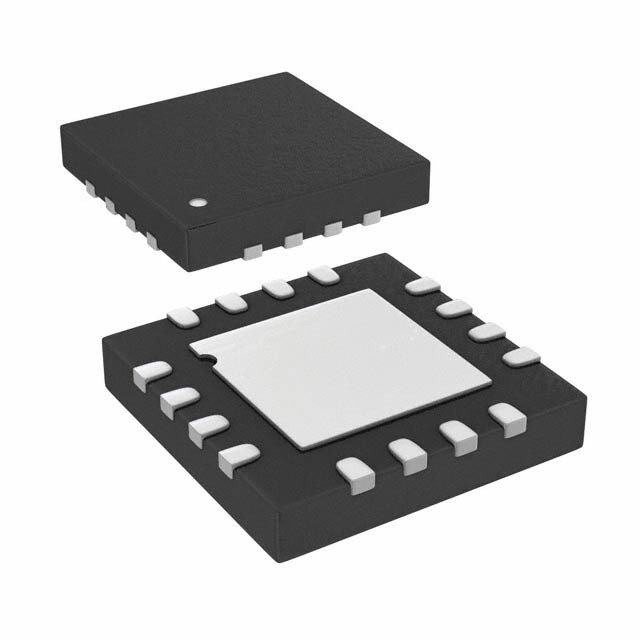
TPS780 www.ti.com SBVS083E–JANUARY2007–REVISEDJANUARY2015 5 Pin Configuration and Functions SOT SON 5Pins 6Pins TopView TopView IN 1 5 OUT OUT 1 6 IN GND 2 Thermal N/C 2 Pad(1) 5 GND EN 3 4 VSET/FB V /FB 3 4 EN SET (1) It is recommended that the SON package thermalpadbeconnectedtoground. PinFunctions PIN I/O DESCRIPTION NAME SON SOT Regulatedoutputvoltagepin.Asmall(1-μF)ceramiccapacitorisneededfromthispinto OUT 1 5 O groundtoassurestability.SeeInputandOutputCapacitorRequirementsformoredetails. N/C 2 — — Notconnected. Feedbackpin(FB)foradjustableversions;V forfixedvoltageversions.Drivetheselect SET V /FB 3 4 I pin(V )below0.4Vtoselectpresetoutputvoltagehigh.DrivetheV pinover1.2V SET SET SET toselectpresetoutputvoltagelow. Enablepin.Drivethispinover1.2Vtoturnontheregulator.Drivethispinbelow0.4Vto EN 4 3 I puttheregulatorintoshutdownmode,reducingoperatingcurrentto18nAtypical. GND 5 2 — Groundpin.Tieallgroundpinstogroundforproperoperation. Inputpin.Asmallcapacitorisneededfromthispintogroundtoassurestability.Atypical IN 6 1 I inputcapacitoris1.0μF.TiebackbothinputandoutputcapacitorgroundtotheIC ground,withnosignificantimpedancebetweenthem. Thermal — — — (SONpackageonly)Connectthethermalpadtoground. pad Copyright©2007–2015,TexasInstrumentsIncorporated SubmitDocumentationFeedback 3 ProductFolderLinks:TPS780
TPS780 SBVS083E–JANUARY2007–REVISEDJANUARY2015 www.ti.com 6 Specifications 6.1 Absolute Maximum Ratings overoperatingfree-airtemperaturerange(unlessotherwisenoted) (1) MIN MAX UNIT V –0.3 +6.0 IN Voltage V andV –0.3 V +0.3(2) V EN VSET IN V –0.3 V +0.3 OUT IN Current I Internallylimited OUT Outputshort-circuitduration Indefinite Totalcontinuouspowerdissipation,P SeeThermalInformation DISS Operatingjunction,T –40 125 °C J Temperature Storage,T –55 150 °C stg (1) StressesbeyondthoselistedunderAbsoluteMaximumRatingsmaycausepermanentdamagetothedevice.Thesearestressratings only,whichdonotimplyfunctionaloperationofthedeviceattheseoranyotherconditionsbeyondthoseindicatedunderRecommended OperatingConditions.Exposuretoabsolute-maximum-ratedconditionsforextendedperiodsmayaffectdevicereliability. (2) V andV absolutemaximumratingareV +0.3Vor+6.0V,whicheverisless. EN VSET IN 6.2 ESD Ratings VALUE UNIT Humanbodymodel(HBM),perANSI/ESDA/JEDECJS-001,allpins(1) ±2000 V(ESD) Electrostaticdischarge Chargeddevicemodel(CDM),perJEDECspecificationJESD22-C101,all V pins(2) ±500 (1) JEDECdocumentJEP155statesthat500-VHBMallowssafemanufacturingwithastandardESDcontrolprocess. (2) JEDECdocumentJEP157statesthat250-VCDMallowssafemanufacturingwithastandardESDcontrolprocess. 6.3 Recommended Operating Conditions overoperatingjunctiontemperaturerange(unlessotherwisenoted) MIN NOM MAX UNIT V Inputvoltage 2.2 5.5 V IN V Outputvoltage 1.8 4.2 V OUT V Enablevoltage 0 V V EN IN I Outputcurrent 0 150 mA OUT T Junctiontemperature –40 125 °C J 6.4 Thermal Information TPS780xx THERMALMETRIC(1) DDC DRV UNIT 5PINS 6PINS R Junction-to-ambientthermalresistance 193.0 65.9 θJA R Junction-to-case(top)thermalresistance 40.1 87.3 θJC(top) R Junction-to-boardthermalresistance 34.3 35.4 θJB °C/W ψ Junction-to-topcharacterizationparameter 0.9 1.7 JT ψ Junction-to-boardcharacterizationparameter 34.1 35.8 JB R Junction-to-case(bottom)thermalresistance N/A 6.1 θJC(bot) (1) Formoreinformationabouttraditionalandnewthermalmetrics,seetheICPackageThermalMetricsapplicationreport,SPRA953. 4 SubmitDocumentationFeedback Copyright©2007–2015,TexasInstrumentsIncorporated ProductFolderLinks:TPS780
TPS780 www.ti.com SBVS083E–JANUARY2007–REVISEDJANUARY2015 6.5 Electrical Characteristics Overoperatingtemperaturerange(T =–40°Cto125°C),V =V +0.5Vor2.2V,whicheverisgreater;I = J IN OUT(nom) OUT 100μA,V =V =V ,C =1.0μF,fixedoradjustable,unlessotherwisenoted.TypicalvaluesatT =25°C. VSET EN IN OUT J PARAMETER TESTCONDITIONS MIN TYP MAX UNIT V Inputvoltagerange 2.2 5.5 V IN Nominal T =25°C,V =high/low –2% ±1% +2% J SET VOUT(1) DCoutputaccuracy OverVIN,IOUT, VOUT(nom)+0.5V≤VIN≤5.5V, –3.0% ±2.0% +3.0% temperature 0mA≤I ≤150mA,V =high/low OUT SET Internalreference(2) V T =25°C,V =4.0V,I =75mA 1.216 V FB (adjustableversiononly) J IN OUT V Outputvoltagerange(3) (4) V =5.5V,I =100μA(2) V 5.25 V OUT_RANGE (adjustableversiononly) IN OUT FB V +0.5V≤V ≤5.5V, ΔV Lineregulation OUT(nom) IN –1% +1% OUT(ΔVIN) I =5mA OUT ΔV Loadregulation 0mA≤I ≤150mA –2% +2% OUT(ΔIOUT) OUT V Dropoutvoltage(5) V =95%V ,I =150mA 250 mV DO IN OUT(nom) OUT BW=100Hzto100kHz,V =2.2V, V Outputnoisevoltage IN 86 μV n V =1.2V,I =1mA RMS OUT OUT V high(outputV selected), V SET OUT(LO) 1.2 V V HI orENhigh(enabled) IN V low(outputV selected), V SET OUT(HI) 0 0.4 V LO orENlow(disabled) I Outputcurrentlimit V =0.90×V 150 230 400 mA CL OUT OUT(nom) I =0mA(6) 420 800 nA OUT I Groundpincurrent GND I =150mA 5 μA OUT V ≤0.4V,2.2V≤V <5.5V, I Shutdowncurrent(I ) EN IN 18 130 nA SHDN GND T =–40°Cto100°C J I V pincurrent V =V =5.5V 70 nA VSET SET EN VSET I ENpincurrent V =V =5.5V 40 nA EN EN VSET FBpincurrent(7) I V =5.5V,V =1.2V,I =100μA 10 nA FB (Adjustableversiononly) IN OUT OUT f=10Hz 40 V =4.3V, IN PSRR Power-supplyrejectionratio V =3.3V, f=100Hz 20 dB OUT I =150mA OUT f=1kHz 15 V transitiontime(high-to-low) V =2.2V,V =3.3V, t OUT OUT_LOW OUT(HI) 800 μs TR(H→L) V =97%×V I =10mA OUT OUT(HI) OUT V transitiontime(low-to-high) V =3.3V,V =2.2V, t OUT OUT_HIGH OUT(LO) 800 μs TR(L→H) V =97%×V I =10mA OUT OUT(LO) OUT t Start-uptime(8) COUT=1.0μF,VOUT=10%VOUT(nom)to 500 μs STR V =90%V OUT OUT(nom) I =150mA,C =1.0μF, OUT OUT t Shutdowntime(9) VOUT=2.8V, 500(10) μs SHDN V =90%V to OUT OUT(nom) V =10%V OUT OUT(nom) Shutdown,temperatureincreasing 160 °C T Thermalshutdowntemperature SD Reset,temperaturedecreasing 140 °C T Operatingjunctiontemperature –40 125 °C J (1) TheoutputvoltageforV =low/highisprogrammedatthefactory. SET (2) Adjustableversiononly. (3) NoV pinontheadjustableversion. SET (4) Nodynamicvoltagescalingontheadjustableversion. (5) V isnotmeasuredfordeviceswithV <2.3VbecauseminimumV =2.2V. DO OUT(nom) IN (6) I =800nA(max)upto100°C. GND (7) TheTPS78001FBpinistiedtoV .Adjustableversiononly. OUT (8) TimefromV =1.2VtoV =90%(V ). EN OUT OUT(nom) (9) TimefromV =0.4VtoV =10%(V ). EN OUT OUT(nom) (10) SeeShutdownformoredetails. Copyright©2007–2015,TexasInstrumentsIncorporated SubmitDocumentationFeedback 5 ProductFolderLinks:TPS780
TPS780 SBVS083E–JANUARY2007–REVISEDJANUARY2015 www.ti.com 6.6 Typical Characteristics OvertheoperatingtemperaturerangeofT =–40°Cto125°C,V =V +0.5Vor2.2V,whicheverisgreater;I = J IN OUT(nom) OUT 100μA,V =V =V ,C =1μF,andC =1μF,unlessotherwisenoted. EN VSET IN OUT IN 0.3 1.0 0.8 0.2 0.6 T = +85°C T = +25°C T =-40°C J J J 0.4 0.1 %) TJ= +125°C TJ= +25°C %) 0.2 (UT 0 (UT 0 VO VO -0.2 -0.1 -0.4 TJ= +125°C -0.2 -0.6 TJ=-40°C TJ= +85°C -0.8 -0.3 -1.0 2.2 2.7 3.2 3.7 4.2 4.7 5.2 5.7 2.7 3.2 3.7 4.2 4.7 5.2 5.7 V (V) V (V) IN IN I =5mA V =1.22V I =5mA V =1.2V V =2.2V OUT OUT(nom) OUT VSET OUT(nom) Figure1.TPS78001LineRegulation Figure2.TPS780330220LineRegulation 3 1.0 0.8 2 0.6 TJ=-40°C T = +25°C J 0.4 1 (%)UT 0 TJ= +25°C TJ=-40°C (%)UT 0.20 VO VO -0.2 -1 -0.4 TJ= +85°C -2 TJ= +85°C -0.6 -0.8 -3 -1.0 2.7 3.2 3.7 4.2 4.7 5.2 5.7 3.8 4.0 4.2 4.4 4.6 4.8 5.0 5.2 5.4 5.6 V (V) V (V) IN IN I =150mA V =1.2V V =2.2V I =5mA V =0.4V V =3.3V OUT VSET OUT(nom) OUT VSET OUT(nom) Figure3.TPS780330220LineRegulation Figure4.TPS780330220LineRegulation 3 1.5 2 1.0 %) 1 TJ=-40°C %) 0.5 TJ= +125°C (UT 0 (UT TJ= +25°C O O V V 0 -1 -2 -0.5 TJ= +85°C TJ= +25°C TJ= +85°C T =-40°C J -3 -1.0 3.8 4.0 4.2 4.4 4.6 4.8 5.0 5.2 5.4 5.6 0 25 50 75 100 125 150 V (V) I (mA) IN OUT I =150mA V =0.4V V =3.3V V =3.3V OUT VSET OUT(nom) OUT(nom) Figure5.TPS780330220LineRegulation Figure6.TPS78001LoadRegulation 6 SubmitDocumentationFeedback Copyright©2007–2015,TexasInstrumentsIncorporated ProductFolderLinks:TPS780
TPS780 www.ti.com SBVS083E–JANUARY2007–REVISEDJANUARY2015 Typical Characteristics (continued) OvertheoperatingtemperaturerangeofT =–40°Cto125°C,V =V +0.5Vor2.2V,whicheverisgreater;I = J IN OUT(nom) OUT 100μA,V =V =V ,C =1μF,andC =1μF,unlessotherwisenoted. EN VSET IN OUT IN 3.0 3 2.5 2 2.0 T =-40°C 1.5 J 1 %) 1.0 %) V(OUT 0.50 TJ=-40°C V(OUT 0 -0.5 -1 -1.0 T = +25°C -2 TJ= +25°C TJ= +85°C -1.5 J T = +85°C -2.0 J -3 0 25 50 75 100 125 150 0 25 50 75 100 125 150 I (mA) I (mA) OUT OUT V =1.2V V =2.7V V =2.2V V =0.4V V =3.8V V =3.3V VSET IN OUT(nom) VSET IN OUT(nom) Figure7.TPS780330220LoadRegulation Figure8.TPS780330220LoadRegulation 200 250 180 TJ= +85°C TJ= +125°C 160 200 ) (mV)UT 114200 TJ= +125°C ) (mV)UT 150 TJ= +85°C O O V 100 V - - VIN 80 VIN 100 ( ( O 60 O D D V V 40 50 20 TJ= +25°C TJ=-40°C TJ= +25°C TJ=-40°C 0 0 0 25 50 75 100 125 150 0 25 50 75 100 125 150 I (mA) I (mA) OUT OUT V =3.3V V =0.95×V V =0.4V V =3.3V V =0.95×V OUT(nom) IN OUT(nom) VSET OUT(nom) IN OUT(nom) Figure9.TPS78001DropoutVoltagevsOutputCurrent Figure10.TPS780330220DropoutVoltagevsOutput Current 250 250 200 200 V) 150mA V) 150mA m m ) (UT 150 ) (UT 150 VO 100mA VO 100mA - - VIN 100 VIN 100 ( ( O 50mA O 50mA D D V V 50 50 10mA 10mA 0 0 -40 -25 -10 5 20 35 50 65 80 95 110 125 -40 -25 -10 5 20 35 50 65 80 95 110 125 Temperature (°C) Temperature (°C) V =3.3 V =0.95×V V =0.4V V =3.3V V =0.95×V OUT(nom) IN OUT(nom) VSET OUT(nom) IN OUT(nom) Figure11.TPS78001DropoutVoltagevsTemperature Figure12.TPS780330220DropoutVoltagevsTemperature Copyright©2007–2015,TexasInstrumentsIncorporated SubmitDocumentationFeedback 7 ProductFolderLinks:TPS780
TPS780 SBVS083E–JANUARY2007–REVISEDJANUARY2015 www.ti.com Typical Characteristics (continued) OvertheoperatingtemperaturerangeofT =–40°Cto125°C,V =V +0.5Vor2.2V,whicheverisgreater;I = J IN OUT(nom) OUT 100μA,V =V =V ,C =1μF,andC =1μF,unlessotherwisenoted. EN VSET IN OUT IN 6 8 TJ= +85°C TJ= +125°C 7 5 T = +125°C T = +85°C J 6 J 4 5 A) A) m m ( 3 ( 4 D D N N G G I I 3 2 T = +25°C 2 TJ= +25°C TJ=-40°C J 1 T =-40°C 1 J 0 0 2.2 2.7 3.2 3.7 4.2 4.7 5.2 5.7 2.2 2.7 3.2 3.7 4.2 4.7 5.2 5.7 V (V) V (V) IN IN I =50mA V =1.22V I =150mA V =1.22V OUT OUT(nom) OUT OUT(nom) Figure13.TPS78001GroundPinCurrentvsInputVoltage Figure14.TPS78001GroundPinCurrentvsInputVoltage 1000 1000 T = +125°C T = +125°C 900 J 900 J 800 800 T = +85°C J 700 700 T = +85°C J A) 600 A) 600 n n ( 500 ( 500 D D N N IG 400 IG 400 300 300 TJ= +25°C TJ=-40°C TJ= +25°C TJ=-40°C 200 200 100 100 0 0 2.7 3.2 3.7 4.2 4.7 5.2 5.7 2.7 3.2 3.7 4.2 4.7 5.2 5.7 V (V) V (V) IN IN I =0mA V =1.2V V =2.2V I =1mA V =1.2V V =2.2V OUT VSET OUT(nom) OUT VSET OUT(nom) Figure15.TPS780330220GroundPinCurrentvsInput Figure16.TPS780330220GroundPinCurrentvsInput Voltage Voltage 6 12 11 5 10 TJ= +85°C TJ= +125°C 9 T = +125°C 4 8 J T = +85°C A) A) 7 J m m ( 3 ( 6 D D GN GN 5 I I 2 4 TJ= +25°C TJ=-40°C 3 T = +25°C 1 2 J T =-40°C 1 J 0 0 2.7 3.2 3.7 4.2 4.7 5.2 5.7 2.7 3.2 3.7 4.2 4.7 5.2 5.7 V (V) V (V) IN IN I =50mA V =1.2V V =2.2V I =150mA V =1.2V V =2.2V OUT VSET OUT(nom) OUT VSET OUT(nom) Figure17.TPS780330220GroundPinCurrentvsInput Figure18.TPS780330220GroundPinCurrentvsInput Voltage Voltage 8 SubmitDocumentationFeedback Copyright©2007–2015,TexasInstrumentsIncorporated ProductFolderLinks:TPS780
TPS780 www.ti.com SBVS083E–JANUARY2007–REVISEDJANUARY2015 Typical Characteristics (continued) OvertheoperatingtemperaturerangeofT =–40°Cto125°C,V =V +0.5Vor2.2V,whicheverisgreater;I = J IN OUT(nom) OUT 100μA,V =V =V ,C =1μF,andC =1μF,unlessotherwisenoted. EN VSET IN OUT IN 1000 1000 900 T = +125°C 900 J T = +125°C J 800 800 T = +85°C T = +25°C J J 700 700 T = +85°C T = +25°C J J A) 600 A) 600 n n ( 500 ( 500 D D N N IG 400 IG 400 300 300 T =-40°C J 200 200 T =-40°C J 100 100 0 0 3.8 4.0 4.2 4.4 4.6 4.8 5.0 5.2 5.4 5.6 3.8 4.0 4.2 4.4 4.6 4.8 5.0 5.2 5.4 5.6 V (V) V (V) IN IN I =0mA V =0.4V V =3.3V I =1mA V =0.4V V =3.3V OUT VSET OUT(nom) OUT VSET OUT(nom) Figure19.TPS780330220GroundPinCurrentvsInput Figure20.TPS780330220GroundPinCurrentvsInput Voltage Voltage 6 9 8 5 TJ= +85°C TJ= +125°C TJ= +85°C TJ= +125°C 7 4 6 A)m A)m 5 ( 3 ( ND ND 4 G G I I 2 3 TJ= +25°C TJ=-40°C 2 TJ= +25°C TJ=-40°C 1 1 0 0 3.8 4.0 4.2 4.4 4.6 4.8 5.0 5.2 5.4 5.6 3.8 4.0 4.2 4.4 4.6 4.8 5.0 5.2 5.4 5.6 V (V) V (V) IN IN I =50mA V =0.4V V =3.3V I =150mA V =0.4V V =3.3V OUT VSET OUT(nom) OUT VSET OUT(nom) Figure21.TPS780330220GroundPinCurrentvsInput Figure22.TPS780330220GroundPinCurrentvsInput Voltage Voltage 10 10 8 8 TJ= +85°C TJ= +125°C TJ= +85°C TJ= +125°C A) 6 A) 6 m m ( ( D D N N IG 4 IG 4 2 2 TJ= +25°C TJ=-40°C TJ= +25°C TJ=-40°C 0 0 0 25 50 75 100 125 150 0 25 50 75 100 125 150 I (mA) I (mA) OUT OUT V =1.2V V =5.5V V =2.2V V =0.4V V =5.5V V =3.3V VSET IN OUT(nom) VSET IN OUT(nom) Figure23.TPS780330220GroundPinCurrentvsOutput Figure24.TPS780330220GroundPinCurrentvsOutput Current Current Copyright©2007–2015,TexasInstrumentsIncorporated SubmitDocumentationFeedback 9 ProductFolderLinks:TPS780
TPS780 SBVS083E–JANUARY2007–REVISEDJANUARY2015 www.ti.com Typical Characteristics (continued) OvertheoperatingtemperaturerangeofT =–40°Cto125°C,V =V +0.5Vor2.2V,whicheverisgreater;I = J IN OUT(nom) OUT 100μA,V =V =V ,C =1μF,andC =1μF,unlessotherwisenoted. EN VSET IN OUT IN 60 280 270 50 T =-40°C J T = +85°C 260 nA) 40 J mit (mA) 250 TJ= +25°C I(GND 3200 TJ= +25°C urrent Li 224300 C 220 T = +85°C 10 J T =-40°C 210 J 0 200 2.2 2.7 3.2 3.7 4.2 4.7 5.2 5.7 2.2 2.7 3.2 3.7 4.2 4.7 5.2 5.7 V (V) V (V) IN IN I =0mA V =0.4V V =90%V V =1.22V OUT VSET OUT OUT(nom) OUT(nom) Figure25.TPS78001ShutdownCurrentvsInputVoltage Figure26.TPS78001CurrentLimitvsInputVoltage 300 300 290 290 280 280 mA) 270 TJ=-40°C mA) 270 TJ=-40°C mit ( 260 mit ( 260 ent Li 225400 TJ= +25°C ent Li 225400 TJ= +25°C Curr 230 TJ= +85°C Curr 230 TJ= +85°C 220 220 T = +125°C T = +125°C J J 210 210 200 200 2.7 3.2 3.7 4.2 4.7 5.2 5.7 3.8 4.0 4.2 4.4 4.6 4.8 5.0 5.2 5.4 5.6 V (V) V (V) IN IN V =1.2V V =95%V V =2.2V V =0.4V V =95%V V =3.3 VSET OUT OUT(nom) OUT(nom) VSET OUT OUT(nom) OUT(nom) V Figure27.TPS780330220CurrentLimitvsInputVoltage Figure28.TPS780330220CurrentLimitvsInputVoltage 5 1.0 4 0.8 A) 3 nA) 0.6 I(nFB 2 (VSET 0.4 TJ= +85°C TJ=-40°C TJ= +25°C I V max IN 1 0.2 V min IN 0 0 -40 -25 -10 5 20 35 50 65 80 95 110 125 2.7 3.2 3.7 4.2 4.7 5.2 5.7 Temperature (°C) V (V) IN I =0mA V =1.22V I =100μA V =1.2V V =2.2V OUT OUT(nom) OUT VSET OUT(nom) Figure29.TPS78001FeedbackPinCurrentvsTemperature Figure30.TPS780330220V PinCurrentvsInputVoltage SET 10 SubmitDocumentationFeedback Copyright©2007–2015,TexasInstrumentsIncorporated ProductFolderLinks:TPS780
TPS780 www.ti.com SBVS083E–JANUARY2007–REVISEDJANUARY2015 Typical Characteristics (continued) OvertheoperatingtemperaturerangeofT =–40°Cto125°C,V =V +0.5Vor2.2V,whicheverisgreater;I = J IN OUT(nom) OUT 100μA,V =V =V ,C =1μF,andC =1μF,unlessotherwisenoted. EN VSET IN OUT IN 2.5 2.0 TJ= +125°C 1.8 2.0 1.6 1.4 1.5 (nA)ET 1.0 (nA)N 11..20 TJ= +85°C TJ= +25°C TJ=-40°C IVS TJ= +85°C TJ=-40°C IE 0.8 0.5 0.6 0.4 0 T = +25°C 0.2 J -0.5 0 3.8 4.0 4.2 4.4 4.6 4.8 5.0 5.2 5.4 5.6 2.2 2.7 3.2 3.7 4.2 4.7 5.2 5.7 V (V) V (V) IN IN I =100μA V =0.4V V =3.3V I =1mA V =1.22V OUT VSET OUT(nom) OUT OUT(nom) Figure31.TPS780330220V PinCurrentvsInputVoltage Figure32.TPS78001EnablePinCurrentvsInputVoltage SET 2.0 2.0 1.8 1.8 1.6 1.6 1.4 1.4 A) (nN 1.2 A) 1.2 IE 10..08 TJ= +85°C TJ= +25°C TJ=-40°C I(nEN 10..08 TJ= +85°C TJ= +25°C TJ=-40°C 0.6 0.6 0.4 0.4 0.2 0.2 0 0 2.7 3.2 3.7 4.2 4.7 5.2 5.7 3.8 4.0 4.2 4.4 4.6 4.8 5.0 5.2 5.4 5.6 V (V) V (V) IN IN I =100μA V =1.2V V =2.2V I =100μA V =0.4V V =3.3V OUT VSET OUT(nom) OUT VSET OUT(nom) Figure33.TPS780330220EnablePinCurrentvsInput Figure34.TPS780330220EnablePinCurrentvsInput Voltage Voltage 1.2 1.2 1.1 1.1 1.0 1.0 V On V On EN EN 0.9 0.9 V) V) (N 0.8 (N 0.8 E E V V 0.7 0.7 V Off V Off EN EN 0.6 0.6 0.5 0.5 0.4 0.4 -40 -25 -10 5 20 35 50 65 80 95 110 125 -40 -25 -10 5 20 35 50 65 80 95 110 125 Temperature (°C) Temperature (°C) I =1mA I =1mA OUT OUT Figure35.TPS78001EnablePinHysteresisvsTemperature Figure36.TPS780330220EnablePinHysteresisvs Temperature Copyright©2007–2015,TexasInstrumentsIncorporated SubmitDocumentationFeedback 11 ProductFolderLinks:TPS780
TPS780 SBVS083E–JANUARY2007–REVISEDJANUARY2015 www.ti.com Typical Characteristics (continued) OvertheoperatingtemperaturerangeofT =–40°Cto125°C,V =V +0.5Vor2.2V,whicheverisgreater;I = J IN OUT(nom) OUT 100μA,V =V =V ,C =1μF,andC =1μF,unlessotherwisenoted. EN VSET IN OUT IN 0.4 1 0.3 0.1mA 0.2 0 %V(V)OUT-00..101 D%V(V)OUT 5mA -1 -0.2 150mA -0.3 -0.4 -2 -40 -25 -10 5 20 35 50 65 80 95 110 125 -40 -25 -10 5 20 35 50 65 80 95 110 125 Temperature (°C) Temperature (°C) I =1mA V =3.8V V =3.3V V =1.2V V =2.7V V =2.2V OUT IN OUT(nom) VSET IN OUT(nom) Figure37.TPS78001%ΔV vsTemperature Figure38.TPS780330220%ΔV vsTemperature OUT OUT 3 100 )z H Ö 2 V/ m 10 D%V(V)OUT --1012 150m5AmA0.1mA put Spectral Noise Density ( 0.00.111 105910mmmVAARMS 10195m0VmRAMS ut 108mV -3 O 0.001 RMS -40 -25 -10 5 20 35 50 65 80 95 110 125 10 100 1k 10k 100k Temperature (°C) Frequency (Hz) V =0.4V V =3.8V V =3.3V C =1μF C =2.2μF V =1.2V VSET IN OUT(nom) IN OUT VSET V =2.7V IN Figure39.TPS780330220%ΔV vsTemperature OUT Figure40.TPS780330220OutputSpectralNoiseDensityvs Frequency 80 1mA VIN VIN= 0.0V to5.0V 70 V VOUT= 3.3V 60 V/div) Enable OUT ICOOUUTT== 1 1500mmFA Cu B) 50 e (1 rren SRR (d 40 50mA Voltag Load Current t (50mA P 30 /d iv 20 0V ) 150mA 10 0 10 100 1k 10k 100k 1M 10M Time (20ms/div) Frequency (Hz) V =2.7V V =1.2V C =2.2μF IN OUT OUT Figure41.TPS78001RippleRejectionvsFrequency Figure42.TPS780330220InputVoltageRampvsOutput Voltage 12 SubmitDocumentationFeedback Copyright©2007–2015,TexasInstrumentsIncorporated ProductFolderLinks:TPS780
TPS780 www.ti.com SBVS083E–JANUARY2007–REVISEDJANUARY2015 Typical Characteristics (continued) OvertheoperatingtemperaturerangeofT =–40°Cto125°C,V =V +0.5Vor2.2V,whicheverisgreater;I = J IN OUT(nom) OUT 100μA,V =V =V ,C =1μF,andC =1μF,unlessotherwisenoted. EN VSET IN OUT IN VIN Enable VSET v) v) V/di VOUT Load Current Cu V/di V Cu Voltage (1 V = 5.5V rrent (50m Voltage (1 Load Current IN rrent (50m IN A A VIOOUUTT== 1 35.03mVA /div) VIN= 0.0V to 5.5V /div) 0V COUT= 10mF 00AV VOUT VICOOUUTT=== 1 210.002mmVFA OUT Time (20ms/div) Time (1ms/div) Figure43.TPS780330220OutputVoltagevsEnable(Slow Figure44.TPS780330220InputVoltagevsDelaytoOutput Ramp) V V IN IN 1V/div 1V/div V = 4.0V to 4.5V VOUT V = 4.0V to 4.5V VOUT IN IN V = 2.2V V = 3.3V OUT OUT I = 150mA I = 150mA OUT OUT Slew Rate = 1V/ms Slew Rate = 1V/ms Time (200ms/div) Time (200ms/div) Figure45.TPS780330220LineTransientResponse Figure46.TPS780330220LineTransientResponse V Enable Enable v) IN v) edi edi Voltag00mV/ V Voltag00mV/ VIN VOUT 1 OUT 1 ( ( V = 5.5V IN VCIOOOUUUTTT=== 5 31m.03AmVFto 15mA CLuorraednt (10mA/div)Current VVIONU=T =5 .35.V3V CLuorraednt (20mA/div)Current I = 17mAto 60mA OUT 0A C = 10mF OUT 0A Time (5ms/div) Time (2ms/div) Figure47.TPS780330220LoadTransientResponse Figure48.TPS780330220LoadTransientResponse Copyright©2007–2015,TexasInstrumentsIncorporated SubmitDocumentationFeedback 13 ProductFolderLinks:TPS780
TPS780 SBVS083E–JANUARY2007–REVISEDJANUARY2015 www.ti.com Typical Characteristics (continued) OvertheoperatingtemperaturerangeofT =–40°Cto125°C,V =V +0.5Vor2.2V,whicheverisgreater;I = J IN OUT(nom) OUT 100μA,V =V =V ,C =1μF,andC =1μF,unlessotherwisenoted. EN VSET IN OUT IN Enable V = 5.5V IN e (1V/div) VIN VOUT Curren e (1V/div) VIN Enable VOUT VICOOOUUUTTT=== 1 315.003mmVFA Curren Voltag Load Current t (50m Voltag Load t (50m A/d Current A/d 0V VIN= 5.50V iv) 0V iv) V = 3.3V OUT I = 150mA OUT C = 10mF OUT Time (1ms/div) Time (1ms/div) Figure49.TPS780330220EnablePinvsOutputVoltage Figure50.TPS780330220EnablePinvsOutputVoltage ResponseandOutputCurrent Delay VOUT VOUT 1V/div VSET 1V/div VSET V = 5.0V IN Enable = V V = 5.0V IN IN I = 150mA I = 150mA OUT OUT V Transitioning from 2.2V to 3.3V V Transitioning from 3.3V to 2.2V OUT OUT Time (500ms/div) Time (500ms/div) Figure51.TPS780330220VSETPinToggle Figure52.TPS780330220VSETPinToggle C V u IN rre n t (5 v) VOUT VSET 0mA V/di /div 1 ) oltage ( VVIONU=T =5 .35.V3V 5100m0mAA V Load Current I = 150mA OUT to 100mA 0A C = 10mF OUT Time (50ms/div) Figure53.TPS780330220VSETPinToggle(SlowRamp) 14 SubmitDocumentationFeedback Copyright©2007–2015,TexasInstrumentsIncorporated ProductFolderLinks:TPS780
TPS780 www.ti.com SBVS083E–JANUARY2007–REVISEDJANUARY2015 7 Detailed Description 7.1 Overview The TPS780 family of low-dropout regulators (LDOs) is designed specifically for battery-powered applications where ultralow quiescent current is a critical parameter. The absence of pulldown circuitry at the output of the LDO provides the flexibility to use the regulator output capacitor as a temporary backup power supply for a short period of time (for example, during battery replacement). The TPS780 family is compatible with the TI MSP430 and other similar products. The enable pin (EN) is compatible with standard CMOS logic. This LDO family is stablewithanyoutputcapacitorgreaterthan1.0µF. 7.2 Functional Block Diagram IN OUT Current Limit Thermal Shutdown X EPROM U M EN Bandgap Active Pull- 10kW (1) Down V /FB SET LOGIC GND (1) Feedbackpin(FB)foradjustableversions;V forfixedvoltageversions. SET 7.3 Feature Description 7.3.1 InternalCurrentLimit The TPS780 is internally current-limited to protect the regulator during fault conditions. During current limit, the output sources a fixed amount of current that is largely independent of output voltage. For reliable operation, do notoperatethedeviceinacurrent-limitstateforextendedperiodsoftime. The PMOS pass element in the TPS780 family has a built-in body diode that conducts current when the voltage at OUT exceeds the voltage at IN. This current is not limited, so if extended reverse voltage operation is anticipated,externallimitingto5%ofratedoutputcurrentmaybeappropriate. Copyright©2007–2015,TexasInstrumentsIncorporated SubmitDocumentationFeedback 15 ProductFolderLinks:TPS780
TPS780 SBVS083E–JANUARY2007–REVISEDJANUARY2015 www.ti.com Feature Description (continued) 7.3.2 Shutdown The enable pin (EN) is active high and is compatible with standard and low-voltage CMOS levels. When shutdowncapabilityisnotrequired,connectENtotheINpin,asshowninFigure54. VIN IN OUT VOUT 1mF 1mF TPS780xx EN GND Figure54. CircuitShowingENTiedHighWhenShutdownCapabilityisnotRequired 7.3.3 ActiveV Pulldown OUT In the TPS780 series, the active pulldown discharges V when the device is off. However, the input voltage OUT mustbegreaterthan2.2Vfortheactivepulldowntowork. 7.4 Device Functional Modes Table1providesaquickcomparisonbetweenthenormal,dropout,anddisabledmodesofoperation. Table1.DeviceFunctionalModeComparison PARAMETER OPERATINGMODE V EN I T IN OUT J Normal V >V +V V >V I <I T <T IN OUT(nom) DO EN EN(HI) OUT CL J SD Dropout V <V +V V >V I <I T <T IN OUT(nom) DO EN EN(HI) OUT CL J SD Disabled — V <V — T >T EN EN(LO) J SD 7.4.1 NormalOperation Thedeviceregulatestothenominaloutputvoltageunderthefollowingconditions: • Theinputvoltageisgreaterthanthenominaloutputvoltageplusthedropoutvoltage(V +V ). OUT(nom) DO • The enable voltage has previously exceeded the enable rising threshold voltage (V > V ) and not yet EN EN(HI) decreasedbelowtheenablefallingthreshold. • Theoutputcurrentislessthanthecurrentlimit(I <I ). OUT CL • Thedevicejunctiontemperatureislessthanthethermalshutdowntemperature(T <T ). J SD 7.4.2 DropoutOperation If the input voltage is lower than the nominal output voltage plus the specified dropout voltage, but all other conditions are met for normal operation, the device operates in dropout mode. In this mode, the output voltage tracks the input voltage. During this mode, the transient performance of the device becomes significantly degraded because the pass device is in a triode state and no longer controls the current through the LDO. Line orloadtransientsindropoutcanresultinlargeoutput-voltagedeviations. 7.4.3 Disabled Thedeviceisdisabledunderthefollowingconditions: • The enable voltage is less than the enable falling threshold voltage (V < V ) or has not yet exceeded EN EN(LO) theenablerisingthreshold. • Thedevicejunctiontemperatureisgreaterthanthethermalshutdowntemperature(T >T ). J SD 16 SubmitDocumentationFeedback Copyright©2007–2015,TexasInstrumentsIncorporated ProductFolderLinks:TPS780
TPS780 www.ti.com SBVS083E–JANUARY2007–REVISEDJANUARY2015 7.5 Programming 7.5.1 ProgrammingtheTPS78001AdjustableLDORegulator The output voltage of the TPS78001 adjustable regulator is programmed using an external resistor divider as showninFigure55.Theoutputvoltageoperatingrangeis1.2Vto5.1V,andiscalculatedusingEquation1: ( R ) V = V ´ 1 + 1 OUT FB R 2 where • V =1.216Vtypical(theinternalreferencevoltage) (1) FB Resistors R and R should be chosen for approximately 1.2-μA divider current. Lower value resistors can be 1 2 used for improved noise performance, but the solution consumes more power. Higher resistor values should be avoided because leakage current into/out of FB across R /R creates an offset voltage that artificially 1 2 increases/decreases the feedback voltage and thus erroneously decreases/increases V . Table 2 lists several OUT common output voltages and resistor values. The recommended design procedure is to choose R = 1 MΩ to set 2 thedividercurrentat1.2 μA,andthencalculateR usingEquation2: 1 ( V ) R = OUT -1 ´R 1 V 2 FB (2) VIN IN OUT VOUT 1mF 1mF R TPS78001 1 EN FB GND R2 R V = V ´(1 + 1 ) OUT FB R 2 Figure55. TPS78001AdjustableLDORegulatorProgramming Table2.OutputVoltageProgrammingGuide OUTPUTVOLTAGE R R 1 2 1.8V 0.499MΩ 1MΩ 2.8V 1.33MΩ 1MΩ 5.0V 3.16MΩ 1MΩ Copyright©2007–2015,TexasInstrumentsIncorporated SubmitDocumentationFeedback 17 ProductFolderLinks:TPS780
TPS780 SBVS083E–JANUARY2007–REVISEDJANUARY2015 www.ti.com 8 Application and Implementation NOTE Information in the following applications sections is not part of the TI component specification, and TI does not warrant its accuracy or completeness. TI’s customers are responsible for determining suitability of components for their purposes. Customers should validateandtesttheirdesignimplementationtoconfirmsystemfunctionality. 8.1 Application Information The TPS780 family of LDOs is factory-programmable to have a fixed output. Note that during start-up or steady- stateconditions,donotallowtheENpinvoltagetoexceedV +0.3V. IN 8.2 Typical Application 4.2V to 5.5V 2.2V to 3.3V VIN IN OUT VOUT 1mF 1mF TPS780 On Off EN V High = V SET OUT(LOW) VSETLow = VOUT(HIGH) VSET GND Figure56. TypicalApplicationCircuit 8.2.1 DesignRequirements Table3.DesignParamters PARAMETER DESIGNREQUIREMENT InputVoltage 5V OutputVoltageHigh 3.6V OutputVoltageLow 2V MaximumOutputCurrent 100mA 8.2.2 DetailedDesignProcedure Selectthedesireddevicebasedontheoutputvoltage. Provide an input supply with adequate headroom to account for dropout and output current to account for the GNDpincurrent,andpowertheload.Selectinputandoutputcapacitorsbasedonapplicationneeds. 8.2.2.1 InputandOutputCapacitorRequirements Although an input capacitor is not required for stability, it is good analog design practice to connect a 0.1-μF to 1.0-μF low equivalent series resistance (ESR) capacitor across the input supply near the regulator. This capacitor counteracts reactive input sources and improves transient response, noise rejection, and ripple rejection. A higher-value capacitor may be necessary if large, fast rise-time load transients are anticipated, or if the device is not located near the power source. If source impedance is not sufficiently low, a 0.1-μF input capacitormaybenecessarytoensurestability. The TPS780 family is designed to be stable with standard ceramic capacitors with values of 1.0 μF or larger at the output. X5R- and X7R-type capacitors are best because they have minimal variation in value and ESR over temperature. Maximum ESR should be less than 1.0 Ω. With tolerance and dc bias effects, the minimum capacitancetoensurestabilityis1μF. 18 SubmitDocumentationFeedback Copyright©2007–2015,TexasInstrumentsIncorporated ProductFolderLinks:TPS780
TPS780 www.ti.com SBVS083E–JANUARY2007–REVISEDJANUARY2015 8.2.2.2 DropoutVoltage The TPS780 family uses a PMOS pass transistor to achieve low dropout. When (V – V ) is less than the IN OUT dropout voltage (V ), the PMOS pass device is the linear region of operation and the input-to-output resistance DO is the R of the PMOS pass element. V approximately scales with output current because the PMOS DS(on) DO device behaves like a resistor in dropout. As with any linear regulator, PSRR and transient response are degraded as (V – V ) approaches dropout. This effect is shown in Typical Characteristics. Refer to IN OUT applicationreportSLVA207,UnderstandingLDODropout,availablefromwww.ti.com. 8.2.2.3 TransientResponse As with any regulator, increasing the size of the output capacitor reduces overshoot and undershoot magnitude butincreasesdurationofthetransientresponse.Formoreinformation,seeFigure48. 8.2.2.4 MinimumLoad The TPS780 family is stable with no output load. Traditional PMOS LDO regulators suffer from lower loop gain at very light output loads. The TPS780 employs an innovative, low-current circuit under very light or no-load conditions, resulting in improved output voltage regulation performance down to zero output current. See for the loadtransientresponse. 8.2.3 ApplicationCurves 100 80 )Hz 1mA ÖV/ 70 m 10 Density ( 1 10195m0VmRAMS B) 6500 al Noise 0.1 PSRR (d 4300 50mA ctr 50mA Spe 0.01 109mVRMS 20 150mA put 1mA 10 ut 108mV O RMS 0.001 0 10 100 1k 10k 100k 10 100 1k 10k 100k 1M 10M Frequency (Hz) Frequency (Hz) C =1μF,C =2.2μF,V =1.2V,V =2.7V V =2.7V,V =1.2V,C =2.2μF IN OUT VSET IN IN OUT OUT Figure57.TPS780330220OutputSpectralNoiseDensity Figure58.TPS78001RippleRejectionvsFrequency vsFrequency 8.3 Do's and Don'ts Placeatleastone1-μFceramiccapacitorascloseaspossibletotheOUTpinoftheregulator. Donotplacetheoutputcapacitormorethan10mmawayfromtheregulator. Connect a 0.1-μF to 1.0-μF low equivalent series resistance (ESR) capacitor across the IN pin and GND of the regulator. Donotexceedtheabsolutemaximumratings. Copyright©2007–2015,TexasInstrumentsIncorporated SubmitDocumentationFeedback 19 ProductFolderLinks:TPS780
TPS780 SBVS083E–JANUARY2007–REVISEDJANUARY2015 www.ti.com 9 Power Supply Recommendations For best performance, connect a low-output impedance power supply directly to the IN pin of the TPS780. Inductive impedances between the input supply and the IN pin create significant voltage excursions at the IN pin duringstart-uporloadtransientevents.Ifinductiveimpedancesareunavoidable,useaninputcapacitor. 9.1 Powering the MSP430 Microcontroller Several versions of the TPS780 are ideal for powering the MSP430 microcontroller. Table 4 shows potential applicationsofsomevoltageversions. Table4.TypicalMSP430Applications V V OUT(HI) OUT(LO) DEVICE (TYP) (TYP) APPLICATION V >1.800Vrequiredbymany OUT,MIN TPS780360200 3.6V 2.0V MSP430s.Allowslowestpower consumptionoperation. V >2.200Vrequiredbysome TPS780360220 3.6V 2.2V OUT,MIN MSP430sFLASHoperation. V >2.700Vrequiredbysome TPS780360300 3.6V 3.0V OUT,MIN MSP430sFLASHoperation. V <3.600Vrequiredbysome TPS780360220 3.6V 2.2V OUT,MIN MSP430s.Allowshighestspeedoperation. The TPS780 family offers many output voltage versions to allow designers to optimize the supply voltage for the processing speed required of the MSP430. This flexible architecture minimizes the supply current consumed by the particular MSP430 application. The MSP430 total system power can be reduced by substituting the 500-nA I TPS780seriesLDOinplaceofanexistingultralowI LDO(typicalbestcase=1μA).Additionally,DVSallows Q Q forincreasingtheclockspeedinactivemode(MSP430V =3.6V).The3.6-VV reducestheMSP430timein CC CC active mode. In low-power mode, MSP430 system power can be further reduced by lowering the MSP430 V to CC 2.2Vinsleepmode. Key features of the TPS780 series are an ultralow quiescent current (500 nA), DVS, and miniaturized packaging. The TPS780 family are available in SON-6 and TSOT-23 packages. Figure 59 shows a typical MSP430 circuit powered by an LDO without DVS. Figure 60 is an MSP430 circuit using a TPS780 LDO that incorporates an integrated DVS, thus simplifying the circuit design. In a circuit without DVS, as Figure 59 illustrates, V is CC always at 3.0 V. When the MSP430 goes into sleep mode, V remains at 3.0 V; if DVS is applied, V could be CC CC reducedinsleepmode.InFigure60,theTPS780LDOwithintegratedDVSmaintains3.6-VV untilalogichigh CC signal from the MSP430 forces V to level shift V from 3.6 V down to 2.2 V, thus reducing power in sleep OUT OUT mode. 20 SubmitDocumentationFeedback Copyright©2007–2015,TexasInstrumentsIncorporated ProductFolderLinks:TPS780
TPS780 www.ti.com SBVS083E–JANUARY2007–REVISEDJANUARY2015 3.0V V V V IN OUT CC 1mF 1mF LDO MSP430 I/O GND V SS V = 3.0V CC 5mA Active Mode 1.6mA I Q LPM3/Sleep Mode Figure59. TypicalLDOWithoutDVS 2.2V to 3.6V V V V IN OUT CC 1mF 1mF TPS780 MSP430 VSET I/O GND V SS V = 3.6V CC V = 2.2V 5mA CC Active Mode 700nA I Q Current LPM3/Sleep Mode Figure60. TPS780WithIntegratedDVS The other benefit of DVS is that it allows a higher V voltage on the MSP430, increasing the clock speed and CC reducingtheactivemodedwelltime. The total system power savings is outlined in Table 5, Table 6, and Table 7. In Table 5, the MSP430 power savings are calculated for various MSP430 devices using a TPS780 series with integrated DVS versus a standard ultralow IQ LDO without DVS. In Table 6, the TPS780 series quiescent power is calculated for a VIN of 4.2V,withthesameVINusedfortheultralowIQLDO.QuiescentpowerdissipationinanLDOistheVINvoltage times the ground current, because zero load is applied. After the dissipation power is calculated for the individual LDOs in Table 6, simple subtraction outputs the LDO power savings using the TPS780 series. Table 7 calculates the total system power savings using a TPS780 series LDO in place of an ultralow IQ 1.2-μA LDO in an MSP430F1121 application. There are many different versions of the MSP430. Actual power savings vary dependingontheselecteddevice. Copyright©2007–2015,TexasInstrumentsIncorporated SubmitDocumentationFeedback 21 ProductFolderLinks:TPS780
TPS780 SBVS083E–JANUARY2007–REVISEDJANUARY2015 www.ti.com Table5.DDVMSP430PowerSavingsWiththeTPS780SeriesonSelectedMSP430Devices LPM3AT LPM3AT LPM3AT LPM3ATVCC=3V,IQ VCC=3.0V×IQ VCC=2.2V,IQ VCC=2.2V×IQ μWSAVINGS DEVICE (μA) (μW) (μA) (μW) USINGONLYDVS MSP430F1121 1.6 4.8 0.7 1.5 3.3 MSP430F149 1.6 4.8 0.9 2.0 2.8 MSP430F2131 0.9 2.7 0.7 1.5 1.2 MSP430F249 1.0 3.0 0.9 2.0 1.0 MSP430F413 0.9 2.7 0.7 1.5 1.2 MSP430F449 1.6 4.8 1.1 2.4 2.4 Table6.TypicalUltralowI LDOQuiescentPowerDissipationvstheTPS780Series Q MSP430SYSTEM TYPICALULTRALOWI TPS780SERIES TPS780SERIESAT25°C POWERSAVINGS Q TYPICALULTRALOWI LDOAT25°CAMBIENT TYPICALI AT25°C AMBIENT,POWER USINGTHETPS780 Q Q LDOAT25°CAMBIENT POWERDISSIPATION AMBIENT DISSIPATION SERIES QuiescentPower I I ×V =4.2V TPS780I I ×V =4.2V Q Q IN Q Q IN DissipationSavings (μA) (μW) (μA) (μW) (μW) 1.20 5.04 0.42 1.76 3.28 Table7.TotalSystemPowerDissipation TOTALSYSTEMPOWERIN LDODISSIPATION MSP430DISSIPATION SLEEPMODE3 Typical1.2μALDO,noDVS 5.04μW 4.8μW(1) 9.84μW TPS780SerieswithDVS 1.76μW 1.5μW(1) 3.26μW (1) ValuetakenfromTable5andrelativetotheMSP430F1121. 10 Layout 10.1 Layout Guidelines 10.1.1 BoardLayoutRecommendationstoImprovePSRRandNoisePerformance To improve ac performance (such as PSRR, output noise, and transient response), design the printed circuit board (PCB) with separate ground planes for V and V , with each ground plane connected only at the GND IN OUT pin of the device. In addition, the output capacitor must be as close as possible to the ground pin of the device to provideacommonreferenceforregulationpurposes.HighESRcapacitorsmaydegradePSRR. 10.1.2 PackageMounting Solder pad footprint recommendations for the TPS780 series are available from the Texas Instruments web site atwww.ti.comthroughtheTPS780seriesproductfolders. 22 SubmitDocumentationFeedback Copyright©2007–2015,TexasInstrumentsIncorporated ProductFolderLinks:TPS780
TPS780 www.ti.com SBVS083E–JANUARY2007–REVISEDJANUARY2015 10.2 Layout Example V V IN OUT 1 5 CIN 2 COUT 3 4 GND PLANE Represents via used for application-specific connections Figure61. TPS780xxDDCPackageLayoutExample 10.3 Thermal Considerations Thermal protection disables the device output when the junction temperature rises to approximately 160°C, allowing the device to cool. After the junction temperature cools to approximately 140°C, the output circuitry is enabled. Depending on power dissipation, thermal resistance, and ambient temperature, the thermal protection circuit may cycle on and off again. This cycling limits the dissipation of the regulator, protecting it from damage asaresultofoverheating. Any tendency to activate the thermal protection circuit indicates excessive power dissipation or an inadequate heatsink. For reliable operation, limit junction temperature to 105°C maximum. To estimate the margin of safety in a complete design (including heatsink), increase the ambient temperature until the thermal protection is triggered;useworst-caseloadsandsignalconditions. The internal protection circuitry of the TPS780 family is designed to protect against overload conditions. However, this circuitry is not intended to replace proper heatsinking. Continuously running the TPS780 series intothermalshutdowndegradesdevicereliability. 10.4 Power Dissipation The ability to remove heat from the die is different for each package type, presenting different considerations in the PCB layout. The PCB area around the device that is free of other components moves the heat from the devicetotheambientair.PerformancedataforJEDEClow-andhigh-KboardsaregiveninThermalInformation. Using heavier copper increases the effectiveness in removing heat from the device. The addition of plated through-holes to heat-dissipating layers also improves the heatsink effectiveness. Power dissipation depends on input voltage and load conditions. Power dissipation (P ) is equal to the product of the output current times the D voltagedropacrosstheoutputpasselement(V toV ),asshowninEquation3: IN OUT P = (V -V )´I D IN OUT OUT (3) Copyright©2007–2015,TexasInstrumentsIncorporated SubmitDocumentationFeedback 23 ProductFolderLinks:TPS780
TPS780 SBVS083E–JANUARY2007–REVISEDJANUARY2015 www.ti.com 11 Device and Documentation Support 11.1 Device Support 11.1.1 DevelopmentSupport 11.1.1.1 EvaluationModules An evaluation module (EVM) is available to assist in the initial circuit performance evaluation using the TPS780. The TPS780XXEVM-301 evaluation module (and related user's guide) can be requested at the Texas InstrumentswebsitethroughtheproductfoldersorpurchaseddirectlyfromtheTIeStore. 11.1.1.2 SpiceModels Computer simulation of circuit performance using SPICE is often useful when analyzing the performance of analogcircuitsandsystems.ASPICEmodelfortheTPS780seriesisavailablethroughtheproductfoldersunder Tools& Software. 11.1.2 DeviceNomenclature Table8.DeviceNomenclature(1) (2) PRODUCT V OUT TPS780vvvxxxyyyz vvvisthenominaloutputvoltageforV andcorrespondstoV pinlow. OUT(HI) SET xxxisthenominaloutputvoltageforV andcorrespondstoV pinhigh. OUT(LO) SET yyyisthepackagedesignator. zisthetapeandreelquantity(R=3000,T=250). Adjustableversion(3)(4) (1) ForthemostcurrentpackageandorderinginformationseethePackageOptionAddendumattheendofthisdocument,orseetheTI websiteatwww.ti.com. (2) Additionaloutputvoltagecombinationsareavailableonaquick-turnbasisusinginnovative,factoryEPROMprogramming.Minimum orderquantitiesapply;contactyoursalesrepresentativefordetailsandavailability. (3) Toordertheadjustableversion,useTPS78001YYYZ. (4) Thedeviceiseitherfixedvoltage,dual-levelV ,oradjustablevoltageonly.Devicedesigndoesnotpermitafixedandadjustable OUT outputsimultaneously. 11.2 Documentation Support 11.2.1 RelatedDocumentation Forrelateddocumentationseethefollowing: • Applicationnote:UnderstandingLDODropout,SLVA207. • TPS780XXEVM-301User'sGuide,SLVU235. 11.3 Trademarks MSP430isatrademarkofTexasInstruments. Allothertrademarksarethepropertyoftheirrespectiveowners. 11.4 Electrostatic Discharge Caution Thesedeviceshavelimitedbuilt-inESDprotection.Theleadsshouldbeshortedtogetherorthedeviceplacedinconductivefoam duringstorageorhandlingtopreventelectrostaticdamagetotheMOSgates. 11.5 Glossary SLYZ022—TIGlossary. Thisglossarylistsandexplainsterms,acronyms,anddefinitions. 24 SubmitDocumentationFeedback Copyright©2007–2015,TexasInstrumentsIncorporated ProductFolderLinks:TPS780
TPS780 www.ti.com SBVS083E–JANUARY2007–REVISEDJANUARY2015 12 Mechanical, Packaging, and Orderable Information The following pages include mechanical, packaging, and orderable information. This information is the most current data available for the designated devices. This data is subject to change without notice and revision of thisdocument.Forbrowser-basedversionsofthisdatasheet,refertotheleft-handnavigation. Copyright©2007–2015,TexasInstrumentsIncorporated SubmitDocumentationFeedback 25 ProductFolderLinks:TPS780
PACKAGE OPTION ADDENDUM www.ti.com 24-Aug-2018 PACKAGING INFORMATION Orderable Device Status Package Type Package Pins Package Eco Plan Lead/Ball Finish MSL Peak Temp Op Temp (°C) Device Marking Samples (1) Drawing Qty (2) (6) (3) (4/5) TPS78001DDCR ACTIVE SOT-23-THIN DDC 5 3000 Green (RoHS CU NIPDAU Level-2-260C-1 YEAR -40 to 125 CEA & no Sb/Br) TPS78001DDCRG4 ACTIVE SOT-23-THIN DDC 5 3000 Green (RoHS CU NIPDAU Level-2-260C-1 YEAR -40 to 125 CEA & no Sb/Br) TPS78001DDCT ACTIVE SOT-23-THIN DDC 5 250 Green (RoHS CU NIPDAU Level-2-260C-1 YEAR -40 to 125 CEA & no Sb/Br) TPS78001DRVR ACTIVE WSON DRV 6 3000 Green (RoHS CU NIPDAU Level-1-260C-UNLIM -40 to 125 CEA & no Sb/Br) TPS78001DRVRG4 ACTIVE WSON DRV 6 3000 Green (RoHS CU NIPDAU Level-1-260C-UNLIM -40 to 125 CEA & no Sb/Br) TPS78001DRVT ACTIVE WSON DRV 6 250 Green (RoHS CU NIPDAU Level-1-260C-UNLIM -40 to 125 CEA & no Sb/Br) TPS780180300DRVR ACTIVE WSON DRV 6 3000 Green (RoHS CU NIPDAU Level-1-260C-UNLIM -40 to 125 RAX & no Sb/Br) TPS780180300DRVT ACTIVE WSON DRV 6 250 Green (RoHS CU NIPDAU Level-1-260C-UNLIM -40 to 125 RAX & no Sb/Br) TPS780230300DRVR ACTIVE WSON DRV 6 3000 Green (RoHS CU NIPDAU Level-1-260C-UNLIM -40 to 125 NXP & no Sb/Br) TPS780230300DRVT ACTIVE WSON DRV 6 250 Green (RoHS CU NIPDAU Level-1-260C-UNLIM -40 to 125 NXP & no Sb/Br) TPS780270200DDCR ACTIVE SOT-23-THIN DDC 5 3000 Green (RoHS CU NIPDAU Level-2-260C-1 YEAR -40 to 125 CVN & no Sb/Br) TPS780270200DDCT ACTIVE SOT-23-THIN DDC 5 250 Green (RoHS CU NIPDAU Level-2-260C-1 YEAR -40 to 125 CVN & no Sb/Br) TPS780300250DRVR ACTIVE WSON DRV 6 3000 Green (RoHS CU NIPDAU | Level-1-260C-UNLIM -40 to 125 OAI & no Sb/Br) CU NIPDAUAG TPS780300250DRVT ACTIVE WSON DRV 6 250 Green (RoHS CU NIPDAU | Level-1-260C-UNLIM -40 to 125 OAI & no Sb/Br) CU NIPDAUAG TPS780330200DDCR ACTIVE SOT-23-THIN DDC 5 3000 Green (RoHS CU NIPDAU Level-2-260C-1 YEAR -40 to 125 13A & no Sb/Br) TPS780330200DDCT ACTIVE SOT-23-THIN DDC 5 250 Green (RoHS CU NIPDAU Level-2-260C-1 YEAR -40 to 125 13A & no Sb/Br) TPS780330220DDCR ACTIVE SOT-23-THIN DDC 5 3000 Green (RoHS CU NIPDAU Level-2-260C-1 YEAR -40 to 125 CEC & no Sb/Br) Addendum-Page 1
PACKAGE OPTION ADDENDUM www.ti.com 24-Aug-2018 Orderable Device Status Package Type Package Pins Package Eco Plan Lead/Ball Finish MSL Peak Temp Op Temp (°C) Device Marking Samples (1) Drawing Qty (2) (6) (3) (4/5) TPS780330220DDCT ACTIVE SOT-23-THIN DDC 5 250 Green (RoHS CU NIPDAU Level-2-260C-1 YEAR -40 to 125 CEC & no Sb/Br) TPS780330220DRVR ACTIVE WSON DRV 6 3000 Green (RoHS CU NIPDAU | Level-1-260C-UNLIM -40 to 125 CEC & no Sb/Br) CU NIPDAUAG TPS780330220DRVT ACTIVE WSON DRV 6 250 Green (RoHS CU NIPDAU | Level-1-260C-UNLIM -40 to 125 CEC & no Sb/Br) CU NIPDAUAG (1) The marketing status values are defined as follows: ACTIVE: Product device recommended for new designs. LIFEBUY: TI has announced that the device will be discontinued, and a lifetime-buy period is in effect. NRND: Not recommended for new designs. Device is in production to support existing customers, but TI does not recommend using this part in a new design. PREVIEW: Device has been announced but is not in production. Samples may or may not be available. OBSOLETE: TI has discontinued the production of the device. (2) RoHS: TI defines "RoHS" to mean semiconductor products that are compliant with the current EU RoHS requirements for all 10 RoHS substances, including the requirement that RoHS substance do not exceed 0.1% by weight in homogeneous materials. Where designed to be soldered at high temperatures, "RoHS" products are suitable for use in specified lead-free processes. TI may reference these types of products as "Pb-Free". RoHS Exempt: TI defines "RoHS Exempt" to mean products that contain lead but are compliant with EU RoHS pursuant to a specific EU RoHS exemption. Green: TI defines "Green" to mean the content of Chlorine (Cl) and Bromine (Br) based flame retardants meet JS709B low halogen requirements of <=1000ppm threshold. Antimony trioxide based flame retardants must also meet the <=1000ppm threshold requirement. (3) MSL, Peak Temp. - The Moisture Sensitivity Level rating according to the JEDEC industry standard classifications, and peak solder temperature. (4) There may be additional marking, which relates to the logo, the lot trace code information, or the environmental category on the device. (5) Multiple Device Markings will be inside parentheses. Only one Device Marking contained in parentheses and separated by a "~" will appear on a device. If a line is indented then it is a continuation of the previous line and the two combined represent the entire Device Marking for that device. (6) Lead/Ball Finish - Orderable Devices may have multiple material finish options. Finish options are separated by a vertical ruled line. Lead/Ball Finish values may wrap to two lines if the finish value exceeds the maximum column width. Important Information and Disclaimer:The information provided on this page represents TI's knowledge and belief as of the date that it is provided. TI bases its knowledge and belief on information provided by third parties, and makes no representation or warranty as to the accuracy of such information. Efforts are underway to better integrate information from third parties. TI has taken and continues to take reasonable steps to provide representative and accurate information but may not have conducted destructive testing or chemical analysis on incoming materials and chemicals. TI and TI suppliers consider certain information to be proprietary, and thus CAS numbers and other limited information may not be available for release. In no event shall TI's liability arising out of such information exceed the total purchase price of the TI part(s) at issue in this document sold by TI to Customer on an annual basis. Addendum-Page 2
PACKAGE OPTION ADDENDUM www.ti.com 24-Aug-2018 Addendum-Page 3
PACKAGE MATERIALS INFORMATION www.ti.com 2-Dec-2018 TAPE AND REEL INFORMATION *Alldimensionsarenominal Device Package Package Pins SPQ Reel Reel A0 B0 K0 P1 W Pin1 Type Drawing Diameter Width (mm) (mm) (mm) (mm) (mm) Quadrant (mm) W1(mm) TPS78001DDCR SOT- DDC 5 3000 179.0 8.4 3.2 3.2 1.4 4.0 8.0 Q3 23-THIN TPS78001DDCT SOT- DDC 5 250 179.0 8.4 3.2 3.2 1.4 4.0 8.0 Q3 23-THIN TPS78001DRVR WSON DRV 6 3000 179.0 8.4 2.2 2.2 1.2 4.0 8.0 Q2 TPS78001DRVR WSON DRV 6 3000 178.0 8.4 2.25 2.25 1.0 4.0 8.0 Q2 TPS78001DRVT WSON DRV 6 250 179.0 8.4 2.2 2.2 1.2 4.0 8.0 Q2 TPS78001DRVT WSON DRV 6 250 178.0 8.4 2.25 2.25 1.0 4.0 8.0 Q2 TPS780180300DRVR WSON DRV 6 3000 179.0 8.4 2.2 2.2 1.2 4.0 8.0 Q2 TPS780180300DRVR WSON DRV 6 3000 178.0 8.4 2.25 2.25 1.0 4.0 8.0 Q2 TPS780180300DRVT WSON DRV 6 250 178.0 8.4 2.25 2.25 1.0 4.0 8.0 Q2 TPS780180300DRVT WSON DRV 6 250 179.0 8.4 2.2 2.2 1.2 4.0 8.0 Q2 TPS780230300DRVR WSON DRV 6 3000 179.0 8.4 2.2 2.2 1.2 4.0 8.0 Q2 TPS780230300DRVR WSON DRV 6 3000 178.0 8.4 2.25 2.25 1.0 4.0 8.0 Q2 TPS780230300DRVT WSON DRV 6 250 178.0 8.4 2.25 2.25 1.0 4.0 8.0 Q2 TPS780230300DRVT WSON DRV 6 250 179.0 8.4 2.2 2.2 1.2 4.0 8.0 Q2 TPS780270200DDCR SOT- DDC 5 3000 179.0 8.4 3.2 3.2 1.4 4.0 8.0 Q3 23-THIN TPS780270200DDCT SOT- DDC 5 250 179.0 8.4 3.2 3.2 1.4 4.0 8.0 Q3 PackMaterials-Page1
PACKAGE MATERIALS INFORMATION www.ti.com 2-Dec-2018 Device Package Package Pins SPQ Reel Reel A0 B0 K0 P1 W Pin1 Type Drawing Diameter Width (mm) (mm) (mm) (mm) (mm) Quadrant (mm) W1(mm) 23-THIN TPS780300250DRVR WSON DRV 6 3000 178.0 8.4 2.25 2.25 1.0 4.0 8.0 Q2 TPS780300250DRVT WSON DRV 6 250 179.0 8.4 2.2 2.2 1.2 4.0 8.0 Q2 TPS780300250DRVT WSON DRV 6 250 178.0 8.4 2.25 2.25 1.0 4.0 8.0 Q2 TPS780330200DDCR SOT- DDC 5 3000 179.0 8.4 3.2 3.2 1.4 4.0 8.0 Q3 23-THIN TPS780330200DDCT SOT- DDC 5 250 179.0 8.4 3.2 3.2 1.4 4.0 8.0 Q3 23-THIN TPS780330220DDCR SOT- DDC 5 3000 179.0 8.4 3.2 3.2 1.4 4.0 8.0 Q3 23-THIN TPS780330220DDCT SOT- DDC 5 250 179.0 8.4 3.2 3.2 1.4 4.0 8.0 Q3 23-THIN TPS780330220DRVR WSON DRV 6 3000 178.0 8.4 2.25 2.25 1.0 4.0 8.0 Q2 TPS780330220DRVT WSON DRV 6 250 178.0 8.4 2.25 2.25 1.0 4.0 8.0 Q2 *Alldimensionsarenominal Device PackageType PackageDrawing Pins SPQ Length(mm) Width(mm) Height(mm) TPS78001DDCR SOT-23-THIN DDC 5 3000 195.0 200.0 45.0 TPS78001DDCT SOT-23-THIN DDC 5 250 195.0 200.0 45.0 TPS78001DRVR WSON DRV 6 3000 203.0 203.0 35.0 TPS78001DRVR WSON DRV 6 3000 205.0 200.0 33.0 PackMaterials-Page2
PACKAGE MATERIALS INFORMATION www.ti.com 2-Dec-2018 Device PackageType PackageDrawing Pins SPQ Length(mm) Width(mm) Height(mm) TPS78001DRVT WSON DRV 6 250 203.0 203.0 35.0 TPS78001DRVT WSON DRV 6 250 205.0 200.0 33.0 TPS780180300DRVR WSON DRV 6 3000 203.0 203.0 35.0 TPS780180300DRVR WSON DRV 6 3000 205.0 200.0 33.0 TPS780180300DRVT WSON DRV 6 250 205.0 200.0 33.0 TPS780180300DRVT WSON DRV 6 250 203.0 203.0 35.0 TPS780230300DRVR WSON DRV 6 3000 203.0 203.0 35.0 TPS780230300DRVR WSON DRV 6 3000 205.0 200.0 33.0 TPS780230300DRVT WSON DRV 6 250 205.0 200.0 33.0 TPS780230300DRVT WSON DRV 6 250 203.0 203.0 35.0 TPS780270200DDCR SOT-23-THIN DDC 5 3000 195.0 200.0 45.0 TPS780270200DDCT SOT-23-THIN DDC 5 250 195.0 200.0 45.0 TPS780300250DRVR WSON DRV 6 3000 205.0 200.0 33.0 TPS780300250DRVT WSON DRV 6 250 203.0 203.0 35.0 TPS780300250DRVT WSON DRV 6 250 205.0 200.0 33.0 TPS780330200DDCR SOT-23-THIN DDC 5 3000 195.0 200.0 45.0 TPS780330200DDCT SOT-23-THIN DDC 5 250 195.0 200.0 45.0 TPS780330220DDCR SOT-23-THIN DDC 5 3000 195.0 200.0 45.0 TPS780330220DDCT SOT-23-THIN DDC 5 250 195.0 200.0 45.0 TPS780330220DRVR WSON DRV 6 3000 205.0 200.0 33.0 TPS780330220DRVT WSON DRV 6 250 205.0 200.0 33.0 PackMaterials-Page3
None
GENERIC PACKAGE VIEW DRV 6 WSON - 0.8 mm max height PLASTIC SMALL OUTLINE - NO LEAD Images above are just a representation of the package family, actual package may vary. Refer to the product data sheet for package details. 4206925/F
PACKAGE OUTLINE DRV0006A WSON - 0.8 mm max height SCALE 5.500 PLASTIC SMALL OUTLINE - NO LEAD B 2.1 A 1.9 PIN 1 INDEX AREA 2.1 1.9 0.8 C 0.7 SEATING PLANE 0.08 C (0.2) TYP 1 0.1 0.05 EXPOSED 0.00 THERMAL PAD 3 4 2X 7 1.3 1.6 0.1 6 1 4X 0.65 0.35 6X PIN 1 ID 0.3 0.25 6X (OPTIONAL) 0.2 0.1 C A B 0.05 C 4222173/B 04/2018 NOTES: 1. All linear dimensions are in millimeters. Any dimensions in parenthesis are for reference only. Dimensioning and tolerancing per ASME Y14.5M. 2. This drawing is subject to change without notice. 3. The package thermal pad must be soldered to the printed circuit board for thermal and mechanical performance. www.ti.com
EXAMPLE BOARD LAYOUT DRV0006A WSON - 0.8 mm max height PLASTIC SMALL OUTLINE - NO LEAD 6X (0.45) (1) 1 7 6X (0.3) 6 SYMM (1.6) (1.1) 4X (0.65) 4 3 (R0.05) TYP SYMM ( 0.2) VIA (1.95) TYP LAND PATTERN EXAMPLE SCALE:25X 0.07 MAX 0.07 MIN ALL AROUND ALL AROUND SOLDER MASK METAL METAL UNDER SOLDER MASK OPENING SOLDER MASK OPENING NON SOLDER MASK DEFINED SOLDER MASK (PREFERRED) DEFINED SOLDER MASK DETAILS 4222173/B 04/2018 NOTES: (continued) 4. This package is designed to be soldered to a thermal pad on the board. For more information, see Texas Instruments literature number SLUA271 (www.ti.com/lit/slua271). 5. Vias are optional depending on application, refer to device data sheet. If some or all are implemented, recommended via locations are shown. www.ti.com
EXAMPLE STENCIL DESIGN DRV0006A WSON - 0.8 mm max height PLASTIC SMALL OUTLINE - NO LEAD SYMM 6X (0.45) METAL 1 7 6X (0.3) 6 (0.45) SYMM 4X (0.65) (0.7) 4 3 (R0.05) TYP (1) (1.95) SOLDER PASTE EXAMPLE BASED ON 0.125 mm THICK STENCIL EXPOSED PAD #7 88% PRINTED SOLDER COVERAGE BY AREA UNDER PACKAGE SCALE:30X 4222173/B 04/2018 NOTES: (continued) 6. Laser cutting apertures with trapezoidal walls and rounded corners may offer better paste release. IPC-7525 may have alternate design recommendations. www.ti.com
IMPORTANTNOTICEANDDISCLAIMER TIPROVIDESTECHNICALANDRELIABILITYDATA(INCLUDINGDATASHEETS),DESIGNRESOURCES(INCLUDINGREFERENCE DESIGNS),APPLICATIONOROTHERDESIGNADVICE,WEBTOOLS,SAFETYINFORMATION,ANDOTHERRESOURCES“ASIS” ANDWITHALLFAULTS,ANDDISCLAIMSALLWARRANTIES,EXPRESSANDIMPLIED,INCLUDINGWITHOUTLIMITATIONANY IMPLIEDWARRANTIESOFMERCHANTABILITY,FITNESSFORAPARTICULARPURPOSEORNON-INFRINGEMENTOFTHIRD PARTYINTELLECTUALPROPERTYRIGHTS. TheseresourcesareintendedforskilleddevelopersdesigningwithTIproducts.Youaresolelyresponsiblefor(1)selectingtheappropriate TIproductsforyourapplication,(2)designing,validatingandtestingyourapplication,and(3)ensuringyourapplicationmeetsapplicable standards,andanyothersafety,security,orotherrequirements.Theseresourcesaresubjecttochangewithoutnotice.TIgrantsyou permissiontousetheseresourcesonlyfordevelopmentofanapplicationthatusestheTIproductsdescribedintheresource.Other reproductionanddisplayoftheseresourcesisprohibited.NolicenseisgrantedtoanyotherTIintellectualpropertyrightortoanythird partyintellectualpropertyright.TIdisclaimsresponsibilityfor,andyouwillfullyindemnifyTIanditsrepresentativesagainst,anyclaims, damages,costs,losses,andliabilitiesarisingoutofyouruseoftheseresources. TI’sproductsareprovidedsubjecttoTI’sTermsofSale(www.ti.com/legal/termsofsale.html)orotherapplicabletermsavailableeitheron ti.comorprovidedinconjunctionwithsuchTIproducts.TI’sprovisionoftheseresourcesdoesnotexpandorotherwisealterTI’sapplicable warrantiesorwarrantydisclaimersforTIproducts. MailingAddress:TexasInstruments,PostOfficeBox655303,Dallas,Texas75265 Copyright©2019,TexasInstrumentsIncorporated