ICGOO在线商城 > 集成电路(IC) > PMIC - 稳压器 - 线性 > XC6201P332PR-G
 Datasheet下载
- 型号: XC6201P332PR-G
- 制造商: TOREX SEMICONDUCTOR
- 库位|库存: xxxx|xxxx
- 要求:
| 数量阶梯 | 香港交货 | 国内含税 |
| +xxxx | $xxxx | ¥xxxx |
查看当月历史价格
查看今年历史价格
XC6201P332PR-G产品简介:
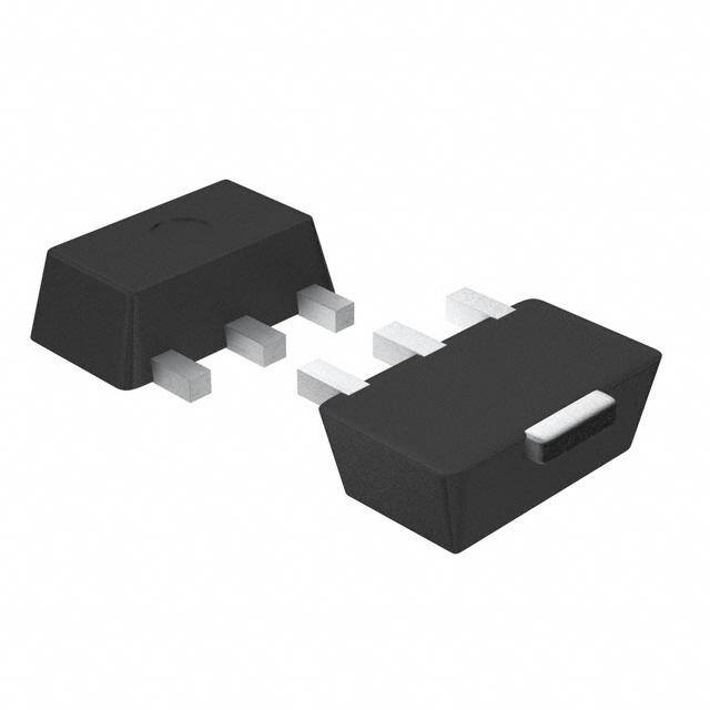
ICGOO电子元器件商城为您提供XC6201P332PR-G由TOREX SEMICONDUCTOR设计生产,在icgoo商城现货销售,并且可以通过原厂、代理商等渠道进行代购。 XC6201P332PR-G价格参考。TOREX SEMICONDUCTORXC6201P332PR-G封装/规格:PMIC - 稳压器 - 线性, Linear Voltage Regulator IC Positive Fixed 1 Output 3.3V 150mA SOT-89。您可以下载XC6201P332PR-G参考资料、Datasheet数据手册功能说明书,资料中有XC6201P332PR-G 详细功能的应用电路图电压和使用方法及教程。
Torex Semiconductor Ltd的XC6201P332PR-G是一款线性稳压器(LDO),属于电源管理集成电路(PMIC)的一部分。该器件常用于需要稳定电压输出、低噪声和高精度调节的电子设备中。

其典型应用场景包括:

1. 便携式电子产品:如智能手机、平板电脑、可穿戴设备等,适用于电池供电系统中为处理器、传感器或其他低功耗模块提供稳定电压。

2. 无线通信模块:如Wi-Fi、蓝牙、Zigbee等无线芯片组供电,因其低噪声特性有助于维持信号完整性。

3. 音频与传感器电路:由于线性稳压器具有较低的输出纹波和噪声,适合为麦克风、扬声器或高精度传感器供电。

4. 工业控制设备:用于PLC、仪表及测量装置中,为敏感模拟电路或微控制器系统提供干净电源。

5. 汽车电子系统:如车载信息娱乐系统、驾驶辅助模块等对电源稳定性要求较高的场景。

该器件采用小型封装,具备良好的负载与线路瞬态响应能力,适合空间受限且对性能有较高要求的设计应用。
| 参数 | 数值 |
| 产品目录 | 集成电路 (IC) |
| 描述 | IC REG LDO 3.3V 0.15A SOT89-3 |
| 产品分类 | |
| 品牌 | Torex Semiconductor Ltd |
| 数据手册 | |
| 产品图片 |
|
| 产品型号 | XC6201P332PR-G |
| rohs | 无铅 / 符合限制有害物质指令(RoHS)规范要求 |
| 产品系列 | - |
| 产品目录页面 | |
| 供应商器件封装 | SOT-89 |
| 其它名称 | 893-1058-6 |
| 包装 | Digi-Reel® |
| 安装类型 | 表面贴装 |
| 封装/外壳 | TO-243AA |
| 工作温度 | -40°C ~ 85°C |
| 标准包装 | 1 |
| 电压-跌落(典型值) | 0.45V @ 160mA |
| 电压-输入 | 最高 10V |
| 电压-输出 | 3.3V |
| 电流-输出 | 150mA |
| 电流-限制(最小值) | - |
| 稳压器拓扑 | 正,固定式 |
| 稳压器数 | 1 |


- 商务部:美国ITC正式对集成电路等产品启动337调查
- 曝三星4nm工艺存在良率问题 高通将骁龙8 Gen1或转产台积电
- 太阳诱电将投资9.5亿元在常州建新厂生产MLCC 预计2023年完工
- 英特尔发布欧洲新工厂建设计划 深化IDM 2.0 战略
- 台积电先进制程称霸业界 有大客户加持明年业绩稳了
- 达到5530亿美元!SIA预计今年全球半导体销售额将创下新高
- 英特尔拟将自动驾驶子公司Mobileye上市 估值或超500亿美元
- 三星加码芯片和SET,合并消费电子和移动部门,撤换高东真等 CEO
- 三星电子宣布重大人事变动 还合并消费电子和移动部门
- 海关总署:前11个月进口集成电路产品价值2.52万亿元 增长14.8%


PDF Datasheet 数据手册内容提取
XC6201 Series ETR0301-007 Positive Voltage Regulators ■GENERAL DESCRIPTION The XC6201 series are highly precise, low power consumption, positive voltage regulators manufactured using CMOS and laser trimming technologies. The series provides large currents with a significantly small dropout voltage. The XC6201 consists of a current limiter circuit, a driver transistor, a precision reference voltage and an error amplifier. Output voltage is selectable in 0.1V steps between 1.3V ~ 6.0V. SOT-25, SOT-89 and USP-6B packages are available. ■APPLICATIONS ■FEATURES ●Smart phones / Mobile phones Maximum Output Current : 250mA (TYP.) Dropout Voltage : 0.16V @ 100mA ●Portable game consoles : 0.40V @ 200mA ●Digital still cameras / Camcorders Maximum Operating Voltage : 10V ●Digital audio equipment Output Voltage Range : 1.3V ~ 6.0V (0.1V increments) ●Reference voltage sources Fixed Voltage Accuracy : ±1% (VOUT(T)>2.0V) ●Multi-function power supplies ±2% Low Power Consumption : 2.0μA (TYP.) Operating Ambient Temperature : -40℃ ~ 85℃ Packages : SOT-25, SOT-89 USP-6B Environmentally Friendly : EU RoHS Compliant, Pb Free Tantalum or Ceramic Capacitor compatible ■TYPICAL APPLICATION CIRCUIT ■TYPICAL PERFORMANCE CHARACTERISTICS ●Supply Current vs. Input Voltage XC6201P332 1/27
XC6201 Series ■BLOCK DIAGRAM ■PRODUCT CLASSIFICATION ●Ordering Information X C 6 2 0 1 P ③④⑤⑥⑦-⑧(*1) ① ② DESIGNATOR ITEM SYMBOL DESCRIPTION ① Product Number 01 - ② Type of Regulator P 3-pin regulator e.g. 30:3.0V ③④ Output Voltage 13~60 50:5.0V 1 ±1% ⑤ Output Voltage Accuracy 2 ±2% MR SOT-25 (3,000pcs/Reel) MR-G SOT-25 (3,000pcs/Reel) Packages PR SOT-89 (1,000pcs/Reel) ⑥⑦-⑧ (Order Unit) PR-G SOT-89 (1,000pcs/Reel) DR USP-6B (3,000pcs/Reel) DR-G USP-6B (3,000pcs/Reel) (*1) The “-G” suffix denotes Halogen and Antimony free as well as being fully EU RoHS compliant. * +1% accuracy can be set at V > 2.0V. OUT(T) 2/27
XC6201 Series ■PIN CONFIGURATION NC VIN VSS NC NC VOUT *The dissipation pad for the USP-6B package should be solder-plated in recommended mount pattern and metal masking so as to enhance mounting strength and heat release. If the pad needs to be connected to other pins, it should be connected to the VSS (No.5) pin. ■PIN ASSIGNMENT PIN NUMBER PIN NAME FUNCTION SOT-25 SOT-89 USP-6B 5 1 3 VOUT Output 2 2 5 VSS Ground 1 3 1 VIN Power Input 3, 4 - 2,4,6 NC No Connection ■ABSOLUTE MAXIMUM RATINGS Ta = 25℃ PARAMETER SYMBOL RATINGS UNITS Input Voltage VIN 12.0 V Output Current IOUT 500 mA Output Voltage VOUT VSS-0.3~VIN+0.3 V SOT-25 250 Power SOT-89 Pd 500 mW Dissipation USP-6B 120 Operating Temperature Topr -40~+85 ℃ Storage Temperature Tstg -55~+125 ℃ 3/27
XC6201 Series ■ELECTRICAL CHARACTERISTICS XC6201P132 VOUT(T)=1.3V (*1) Ta=25℃ PARAMETER SYMBOL CONDITIONS MIN. TYP. MAX. UNITS CIRCUIT Output Voltage VOUT(E) (*2) VIN=2.3V 1.274 1.300 1.326 V ② IOUT=10mA Maximum Output Current I VIN=2.3V 60 - - mA ② OUTmax VOUT(E)≧1.17V Load Regulation △VOUT 1mA≦VINIO=U2T.≦3V3 0mA - 10 30 mV ② Dropout Voltage (*3) Vdif1 IOUT=30mA - 200 600 mV ② Vdif2 IOUT=60mA - 500 810 Supply Current ISS VIN=2.3V - 2.0 5.0 μA ① Line Regulation △VOUT IOUT=10mA - 0.2 0.3 %/V ② △VIN・△VOUT 2.3V≦VIN≦10.0V Input Voltage VIN 1.8 - 10 V - Output Voltage △VOUT IOUT=40mA - ±100 - ppm/℃ ② Temperature Characteristics △Topr・△VOUT -40℃≦Topr≦85℃ XC6201P182 VOUT(T)=1.8V (*1) Ta=25℃ PARAMETER SYMBOL CONDITIONS MIN. TYP. MAX. UNITS CIRCUIT Output Voltage VOUT(E) (*2) VIN=2.8V 1.764 1.800 1.836 V ② IOUT=40mA Maximum Output Current IOUTmax VOUVTI(NE=)≧2.18.V6 2V 80 - - mA ② Load Regulation △VOUT 1mA≦VINIO=U2T.≦8V4 0mA - 10 30 mV ② Dropout Voltage (*3) Vdif1 IOUT=40mA - 200 370 mV ② Vdif2 IOUT=80mA - 450 710 Supply Current ISS VIN=2.8V - 2.0 5.0 μA ① Line Regulation △VOUT IOUT=40mA - 0.2 0.3 %/V ② △VIN・△VOUT 2.8V≦VIN≦10.0V Input Voltage VIN 1.8 - 10 V - Output Voltage △VOUT IOUT=40mA - ±100 - ppm/℃ ② Temperature Characteristics △Topr・△VOUT -40℃≦Topr≦85℃ XC6201P272 VOUT(T)=2.7V (*1) Ta=25℃ PARAMETER SYMBOL CONDITIONS MIN. TYP. MAX. UNITS CIRCUIT Output Voltage VOUT(E) (*2) VIN=3.7V 2.646 2.700 2.754 V ② IOUT=40mA Maximum Output Current IOUTmax VOUVTI(NE=)≧3.27.V4 3V 100 - - mA ② Load Regulation △VOUT 1mA≦VINIO=U3T.≦7V6 0mA - 15 40 mV ② Dropout Voltage (*3) Vdif1 IOUT=60mA - 200 370 mV ② Vdif2 IOUT=120mA - 450 710 Supply Current ISS VIN=3.7V - 2.0 5.0 μA ① Line Regulation △VOUT IOUT=40mA - 0.2 0.3 %/V ② △VIN・△VOUT 3.7V≦VIN≦10.0V Input Voltage VIN 1.8 - 10 V - Output Voltage △VOUT IOUT=40mA - ±100 - ppm/℃ ② Temperature Characteristics △Topr・△VOUT -40℃≦Topr≦85℃ 4/27
XC6201 Series ■ELECTRICAL CHARACTERISTICS (Continued) XC6201P332 VOUT(T)=3.3V (*1) Ta=25℃ PARAMETER SYMBOL CONDITIONS MIN. TYP. MAX. UNITS CIRCUIT Output Voltage VOUT(E) (*2) VIN=4.3V 3.234 3.300 3.366 V ② IOUT=40mA Maximum Output Current IOUTmax VOUVTI(NE=)≧4.23.V9 7V 150 - - mA ② Load Regulation △VOUT 1mA≦VINIO=U4T.≦3V8 0mA - 20 50 mV ② Dropout Voltage (*3) Vdif1 IOUT=80mA - 200 360 mV ② Vdif2 IOUT=160mA - 450 700 Supply Current ISS VIN=4.3V - 2.0 5.0 μA ① Line Regulation △VOUT IOUT=40mA - 0.2 0.3 %/V ② △VIN・△VOUT 4.3V≦VIN≦10.0V Input Voltage VIN 1.8 - 10 V - Output Voltage △VOUT IOUT=40mA - ±100 - ppm/℃ ② Temperature Characteristics △Topr・△VOUT -40℃≦Topr≦85℃ XC6201P502 VOUT(T)=5.0V (*1) Ta=25℃ PARAMETER SYMBOL CONDITIONS MIN. TYP. MAX. UNITS CIRCUIT Output Voltage VOUT(E) (*2) VIN=6.0V 4.900 5.000 5.100 V ② IOUT=40mA Maximum Output Current IOUTmax VOUVTI(NE=)≧6.40.V5 7V 200 - - mA ② Load Regulation △VOUT 1mA≦VIINO=UT6≦.01V0 0mA - 30 70 mV ② Dropout Voltage (*3) Vdif1 IOUT=100mA - 160 340 mV ② Vdif2 IOUT=200mA - 400 600 Supply Current ISS VIN=6.0V - 2.0 6.0 μA ① Line Regulation △VOUT IOUT=40mA - 0.2 0.3 %/V ② △VIN・△VOUT 6.0V≦VIN≦10.0V Input Voltage VIN 1.8 - 10 V - Output Voltage △VOUT IOUT=40mA - ±100 - ppm/℃ ② Temperature Characteristics △Topr・△VOUT -40℃≦Topr≦85℃ NOTE: *1: V = Nominal output voltage. OUT(T) *2: V = Effective output voltage (i.e. the output voltage when “V +1.0V” is provided while OUT(E) OUT(T) maintaining a certain I value). OUT *3: Vdif = (VIN1- VOUT1) VIN1 :An Input Voltage when V appears as the input voltage is gradually decreased. OUT1 V : A voltage equal to 98% of the output voltage when a stabilized (V + 1.0V) is input. OUT1 OUT(T) 5/27
XC6201 Series ■TEST CIRCUITS Circuit ① : Supply Current Circuit ② : Output Voltage, Oscillation, Line Regulation, Dropout Voltage, Load Regulation 6/27
XC6201 Series ■OPERATIONAL EXPLANATION (Tantalum) (Tantalum) With the XC6201 series regulator, in order to ensure the stabilized output voltage, we suggest that an output capacitor (CL) of 1μF or more be connected between the output pin (VOUT) and the VSS pin. For using low ESR capacitor (e.g. ceramic capacitors), please make sure that the output voltage is more than 1.7V. When the output voltage is from 1.3V to 1.6V, the output capacitor should be a tantalum capacitor with a capacitance of 2.2μF. We also suggest an input capacitor (CIN) should be connected between the VIN and the VSS in order to stabilize input power source. OUTPUT VOLTAGE CIN CL (TANTALUM) CL (LOW ESR) 1.3V~1.6V ≧1.0μF ≧2.2μF - 1.7V~6.0V ≧1.0μF ≧1.0μF ≧1.0μF VIN=1.8V~10V,VOUT=1.7~6.0V CIN=1.0μF(Ceramic),CL=1.0μF(ceramic) 7/27
XC6201 Series ■ NOTE ON USE 1. Please use this IC within the stated absolute maximum ratings. The IC is liable to malfunction should the ratings be exceeded. When a voltage higher than the VIN flows to the VOUT like when using two power supplies, please connect a Schottky barrier diode between the VOUT and the VIN and do not exceed the VOUT rating. 2. An oscillation may occur by the impedance between a power supply and the input of the IC. Where the impedance is 10Ωor more, please use an input capacitor (CIN) of at least 1μF. In case of high output current, operation can be stabilized by increasing the input capacitor value. Also an oscillation may occur if the input capacitor value is smaller than the input impedance when the output capacitance (CL) is large. In such cases, operations can be stabilized by either increasing the input capacitor value or reducing the output capacitor value. 3. Please ensure that output current (IOUT) is less than Pd / (VIN - VOUT) and do not exceed the rated power dissipation value (Pd) of the package. 8/27
XC6201 Series ■TYPICAL PERFORMANCE CHARACTERISTICS (1) Output Voltage vs. Output Current 9/27
XC6201 Series ■TYPICAL PERFORMANCE CHARACTERISTICS (Continued) (2) Output Voltage vs. Input Voltage XC6201P132 XC6201P132 XC6201P182 XC6201P182 XC6201P272 XC6201P272 10/27
XC6201 Series ■TYPICAL PERFORMANCE CHARACTERISTICS (Continued) (2) Output Voltage vs. Input Voltage (Continued) XC6201P332 XC6201P332 XC6201P502 XC6201P502 11/27
XC6201 Series ■TYPICAL PERFORMANCE CHARACTERISTICS (Continued) (3) Dropout Voltage vs. Output Current XC6201P132 XC6201P182 XC6201P272 XC6201P332 XC6201P502 12/27
XC6201 Series ■TYPICAL PERFORMANCE CHARACTERISTICS (Continued) (4) Supply Current vs. Input Voltage XC6201P132 XC6201P132 XC6201P182 13/27
XC6201 Series ■TYPICAL PERFORMANCE CHARACTERISTICS (Continued) (4) Supply Current vs. Input Voltage (Continued) XC6201P332 14/27
XC6201 Series ■TYPICAL PERFORMANCE CHARACTERISTICS (Continued) (5) Output Voltage vs. Ambient Temperature 15/27
XC6201 Series ■TYPICAL PERFORMANCE CHARACTERISTICS (Continued) (6) Supply Current vs. Ambient Temperature 16/27
XC6201 Series ■TYPICAL PERFORMANCE CHARACTERISTICS (Continued) (7) Input Transient Response XC6201P132 XC6201P182 Time (1ms/div) Time (1ms/div) XC6201P272 XC6201P332 Time (1ms/div) Time (1ms/div) XC6201P502 Time (1ms/div) 17/27
XC6201 Series ■TYPICAL PERFORMANCE CHARACTERISTICS (Continued) (8) Load Transient Response XC6201P132 XC6201P182 Time (2ms/div) Time (2ms/div) XC6201P272 XC6201P332 Time (2ms/div) Time (2ms/div) XC6201P502 Time (2ms/div) 18/27
XC6201 Series ■TYPICAL PERFORMANCE CHARACTERISTICS (Continued) (9) Ripple Rejection Rate XC6201P132 XC6201P182 XC6201P272 XC6201P332 XXCC66220011PP550022 (10) Output Noise Density XC6201P302 19/27
XC6201 Series ■PACKAGING INFORMATION ●SOT-25 ●SOT-25 Reference Pattern Layout Unit : mm 2.9±0.2 0.7 +0.1 0.4 -0.05 5 4 0~0.1 +0.21.6-0.1 2.8±0.2 N MI 0.2 1 2 3 4 . +0.1 2 (0.95) 0.15 -0.05 1.9±0.2 0 . 1 1.1±0.1 1.3MAX 0.95 0.95 ●SOT-89 Unit : mm ●SOT-89 Reference Pattern Layout 4 . 4 5 1.4 1.2 85 1.4 . 0 0.8 0.8 0.8 1.5 1.5 20/27
XC6201 Series ■PACKAGING INFORMATION (Continued) ●USP-6B Unit : mm ●USP-6B Reference Pattern Layout ●USP-6B Reference Metal Mask Design 21/27
XC6201 Series ● SOT-25 Power Dissipation Power dissipation data for the SOT-25 is shown in this page. The value of power dissipation varies with the mount board conditions. Please use this data as the reference data taken in the following condition. 1. Measurement Condition 40.0 Condition: Mount on a board 28.9 Ambient: Natural convection Soldering: Lead (Pb) free Board: Dimensions 40 x 40 mm (1600 mm2 in one side) Copper (Cu) traces occupy 50% of the board area In top and back faces Package heat-sink is tied to the copper traces (Board of SOT-26 is used.) Material: Glass Epoxy (FR-4) Thickness: 1.6mm Through-hole: 4 x 0.8 Diameter 2.54 1.4 Evaluation Board (Unit:mm) 2.Power Dissipation vs. Ambient Temperature Board Mount (Tj max = 125℃) Ambient Temperature(℃) Power Dissipation Pd(mW) Thermal Resistance (℃/W) 25 600 166.67 85 240 Pd vs. Ta 700 ) W m 600 ( d P 500 n o ati 400 p si 300 s Di er 200 w Po 100 0 25 45 65 85 105 125 Ambient Temperature Ta (℃) 22/27
XC6201 Series ● SOT-89 Power Dissipation Power dissipation data for the SOT-89 is shown in this page. The value of power dissipation varies with the mount board conditions. Please use this data as the reference data taken in the following condition. 1. Measurement Condition Condition: Mount on a board Ambient: Natural convection Soldering: Lead (Pb) free Board: Dimensions 40 x 40 mm (1600 mm2 in one side) Caroepap Ienr t(oCpu )a ntrda cbeasc ko cfaccuepsy 50% of the board 28.9 40.0 Package heat-sink is tied to the copper traces Material: Glass Epoxy (FR-4) Thickness: 1.6mm Through-hole: 5 x 0.8 Diameter 5 2. Evaluation Board (Unit:mm) 2.Power Dissipation vs. Ambient Temperature Board Mount (Tj max = 125℃) Ambient Temperature(℃) Power Dissipation Pd(mW) Thermal Resistance (℃/W) 25 1000 100.00 85 400 Pd vs Ta 1200 W 1000 m ( d 800 P n o 600 ati p si 400 s Di er 200 w o P 0 25 45 65 85 105 125 Ambient Temperature Ta (℃) 23/27
XC6201 Series ● USP-6B Power Dissipation Power dissipation data for theUSP-6B is shown in this page. The value of power dissipation varies with the mount board conditions. Please use this data as the reference data taken in the following condition. 1. Measurement Condition Condition: Mount on a board Ambient: Natural convection Soldering: Lead (Pb) free Board: Dimensions 40 x 40 mm (1600 mm2 in one side) Copper (Cu) traces occupy 50% of the board 28.9 40.0 area In top and back faces Package heat-sink is tied to the copper traces Material: Glass Epoxy (FR-4) Thickness: 1.6mm Through-hole: 4 x 0.8 Diameter 5 2. Evaluation Board (Unit:mm) 2.Power Dissipation vs. Ambient Temperature Board Mount (Tj max = 125℃) Ambient Temperature(℃) Power Dissipation Pd(mW) Thermal Resistance (℃/W) 25 1000 100.00 85 400 Pd vs. Ta 1200 ) W 1000 m ( d 800 P n atio 600 p si 400 s Di er 200 w o P 0 25 45 65 85 105 125 Ambient Temperature Ta (℃) 24/27
XC6201 Series ■MARKING RULE ●SOT-89, SOT-25 ① represents the product series MARK PRODUCT SERIES ② ④ 1 XC6201xxxxxx ① ③ ② represents type of regulator 1 2 3 MARK PRODUCT SERIES SOT-89 Voltage= 0.1 ~ 3.0V Voltage= 3.1 ~ 6.0V (TOP VIEW) 5 6 XC6201Pxxxxx 8 9 XC6201TxxxPx 5 4 ③ represents output voltage ① ② ③ ④ MARK OUTPUT VOLTAGE (V) MARK OUTPUT VOLTAGE (V) 0 - 3.1 - F 1.6 4.6 - 1 2 3 1 - 3.2 - H 1.7 4.7 - 2 - 3.3 - K 1.8 4.8 - SOT-25 3 - 3.4 - L 1.9 4.9 - (TOP VIEW) 4 - 3.5 - M 2.0 5.0 - 5 - 3.6 - N 2.1 5.1 - 6 - 3.7 - P 2.2 5.2 - 7 - 3.8 - R 2.3 5.3 - 8 - 3.9 - S 2.4 5.4 - 9 - 4.0 - T 2.5 5.5 - A - 4.1 - U 2.6 5.6 - B - 4.2 - V 2.7 5.7 - C 1.3 4.3 - X 2.8 5.8 - D 1.4 4.4 - Y 2.9 5.9 - E 1.5 4.5 - Z 3.0 6.0 - ④ represents assembly lot number 0 to 9, A to Z repeated (G, I, J, O, Q, W excluded) 25/27
XC6201 Series ■MARKING RULE (Continued) ●USP-6B ①② represents product series ③ represents type of regulator USP-6B (TOP VIEW) MARK TYPE PRODUCT SERIES P 3pin Regulator XC6201PxxxDx T VIN=7V(Rated) XC6201TxxxDx ④⑤ represents output voltage MARK VOLTAGE (V) PRODUCT SERIES ④ ⑤ 3 3 3.3 XC6201x33xDx 5 0 5.0 XC6201x50xDx ⑥ represents assembly lot number 0 to 9, A to Z repeated (G, I, J, O, Q, W excluded) Note: No character inversion used. 26/27
XC6201 Series 1. The product and product specifications contained herein are subject to change without notice to improve performance characteristics. Consult us, or our representatives before use, to confirm that the information in this datasheet is up to date. 2. The information in this datasheet is intended to illustrate the operation and characteristics of our products. We neither make warranties or representations with respect to the accuracy or completeness of the information contained in this datasheet nor grant any license to any intellectual property rights of ours or any third party concerning with the information in this datasheet. 3. Applicable export control laws and regulations should be complied and the procedures required by such laws and regulations should also be followed, when the product or any information contained in this datasheet is exported. 4. The product is neither intended nor warranted for use in equipment of systems which require extremely high levels of quality and/or reliability and/or a malfunction or failure which may cause loss of human life, bodily injury, serious property damage including but not limited to devices or equipment used in 1) nuclear facilities, 2) aerospace industry, 3) medical facilities, 4) automobile industry and other transportation industry and 5) safety devices and safety equipment to control combustions and explosions. Do not use the product for the above use unless agreed by us in writing in advance. 5. Although we make continuous efforts to improve the quality and reliability of our products; nevertheless Semiconductors are likely to fail with a certain probability. So in order to prevent personal injury and/or property damage resulting from such failure, customers are required to incorporate adequate safety measures in their designs, such as system fail safes, redundancy and fire prevention features. 6. Our products are not designed to be Radiation-resistant. 7. Please use the product listed in this datasheet within the specified ranges. 8. We assume no responsibility for damage or loss due to abnormal use. 9. All rights reserved. No part of this datasheet may be copied or reproduced unless agreed by Torex Semiconductor Ltd in writing in advance. TOREX SEMICONDUCTOR LTD. 27/27