ICGOO在线商城 > 集成电路(IC) > PMIC - 稳压器 - 线性 > TPS71712DCKT
 Datasheet下载
- 型号: TPS71712DCKT
- 制造商: Texas Instruments
- 库位|库存: xxxx|xxxx
- 要求:
| 数量阶梯 | 香港交货 | 国内含税 |
| +xxxx | $xxxx | ¥xxxx |
查看当月历史价格
查看今年历史价格
TPS71712DCKT产品简介:
ICGOO电子元器件商城为您提供TPS71712DCKT由Texas Instruments设计生产,在icgoo商城现货销售,并且可以通过原厂、代理商等渠道进行代购。 TPS71712DCKT价格参考。Texas InstrumentsTPS71712DCKT封装/规格:PMIC - 稳压器 - 线性, Linear Voltage Regulator IC Positive Fixed 1 Output 1.2V 150mA SC-70-5。您可以下载TPS71712DCKT参考资料、Datasheet数据手册功能说明书,资料中有TPS71712DCKT 详细功能的应用电路图电压和使用方法及教程。
TPS71712DCKT 是由德州仪器(Texas Instruments)生产的一款低功耗、低噪声线性稳压器,属于 PMIC(电源管理集成电路)中的线性稳压器类别。以下是其主要应用场景:

 1. 便携式电子设备
TPS71712DCKT 具有低静态电流(典型值为950 nA),非常适合用于电池供电的便携式设备,例如:
- 智能手表和健身追踪器
- 可穿戴健康监测设备
- 无线耳机(TWS耳机)
这些设备需要高效的电源管理以延长电池寿命。

 2. 物联网 (IoT) 设备
由于其高效率和小封装尺寸(如 DCKT 封装),TPS71712DCKT 广泛应用于各种 IoT 设备中,包括:
- 传感器节点
- 无线模块(如 Zigbee、Bluetooth Low Energy)
- 智能家居控制器

 3. 工业应用
在工业领域,TPS71712DCKT 的稳定性和可靠性使其适用于以下场景:
- 数据采集系统
- 工业自动化设备
- 远程监控装置

 4. 通信设备
该稳压器具有良好的瞬态响应和低噪声特性,适合为通信设备中的敏感电路供电,例如:
- 基站中的射频前端电路
- 无线通信模块

 5. 汽车电子
尽管 TPS71712DCKT 主要面向消费级和工业级市场,但在某些非关键汽车应用中也可以使用,例如:
- 车载信息娱乐系统
- 传感器接口

 特性支持的应用需求:
- 输出电压固定为 1.2 V,适用于为低功耗 MCU 和 DSP 供电。
- 高 PSRR(电源抑制比)和低输出噪声,确保对噪声敏感的模拟电路正常工作。
- 宽输入电压范围(1.7 V 至 6.5 V),适应多种电源环境。

总之,TPS71712DCKT 凭借其高效、低功耗和高稳定性,广泛应用于需要长时间运行且对电源质量要求较高的场景。
| 参数 | 数值 |
| 产品目录 | 集成电路 (IC)半导体 |
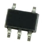
| 描述 | IC REG LDO 1.2V 0.15A SC70-5低压差稳压器 150mA Fixed (1.2V) Lo Noise Hi PSRR |
| 产品分类 | |
| 品牌 | Texas Instruments |
| 产品手册 | |
| 产品图片 |
|
| rohs | 符合RoHS无铅 / 符合限制有害物质指令(RoHS)规范要求 |
| 产品系列 | 电源管理 IC,低压差稳压器,Texas Instruments TPS71712DCKT- |
| 数据手册 | |
| 产品型号 | TPS71712DCKT |
| 产品种类 | 低压差稳压器 |
| 供应商器件封装 | SC-70-5 |
| 其它名称 | 296-32536-2 |
| 制造商产品页 | http://www.ti.com/general/docs/suppproductinfo.tsp?distId=10&orderablePartNumber=TPS71712DCKT |
| 包装 | 带卷 (TR) |
| 商标 | Texas Instruments |
| 安装类型 | 表面贴装 |
| 安装风格 | SMD/SMT |
| 封装 | Reel |
| 封装/外壳 | 6-TSSOP(5 引线),SC-88A,SOT-353 |
| 封装/箱体 | SC-70-5 |
| 工作温度 | -40°C ~ 125°C |
| 工厂包装数量 | 250 |
| 最大功率耗散 | 0.32 W |
| 最大工作温度 | + 125 C |
| 最大输入电压 | 6.5 V |
| 最小工作温度 | - 40 C |
| 最小输入电压 | + 2.5 V |
| 标准包装 | 250 |
| 电压-跌落(典型值) | - |
| 电压-输入 | 2.5 V ~ 6.5 V |
| 电压-输出 | 1.2V |
| 电压调节准确度 | 3 % |
| 电流-输出 | 150mA |
| 电流-限制(最小值) | 200mA |
| 稳压器拓扑 | 正,固定式 |
| 稳压器数 | 1 |
| 系列 | TPS71712 |
| 线路调整率 | 125 uV / V |
| 负载调节 | 120 uV / mA |
| 输入偏压电流—最大 | 0.05 mA |
| 输出电压 | 1.2 V |
| 输出电流 | 150 mA |
| 输出端数量 | 1 Output |
| 输出类型 | Fixed |
| 配用 | /product-detail/zh/TPS717XXEVM-134/296-19614-ND/1014189 |


- 商务部:美国ITC正式对集成电路等产品启动337调查
- 曝三星4nm工艺存在良率问题 高通将骁龙8 Gen1或转产台积电
- 太阳诱电将投资9.5亿元在常州建新厂生产MLCC 预计2023年完工
- 英特尔发布欧洲新工厂建设计划 深化IDM 2.0 战略
- 台积电先进制程称霸业界 有大客户加持明年业绩稳了
- 达到5530亿美元!SIA预计今年全球半导体销售额将创下新高
- 英特尔拟将自动驾驶子公司Mobileye上市 估值或超500亿美元
- 三星加码芯片和SET,合并消费电子和移动部门,撤换高东真等 CEO
- 三星电子宣布重大人事变动 还合并消费电子和移动部门
- 海关总署:前11个月进口集成电路产品价值2.52万亿元 增长14.8%


PDF Datasheet 数据手册内容提取
Product Sample & Technical Tools & Support & Reference Folder Buy Documents Software Community Design TPS717 SBVS068I–FEBRUARY2006–REVISEDJANUARY2016 TPS717 Low-Noise, High-Bandwidth PSRR, Low-Dropout, 150-mA Linear Regulator 1 Features 3 Description • InputVoltage:2.5Vto6.5V The TPS717 family of low-dropout (LDO), low-power 1 linear regulators offers very high power-supply • AvailableinMultipleOutputVersions: rejection (PSRR) while maintaining very low 45-μA – FixedOutputwithVoltagesfrom0.9Vto5V ground current in an ultra-small, five-pin SOT – AdjustableOutputVoltagefrom0.9Vto6.2V package. The family uses an advanced BiCMOS process and a PMOS pass device to achieve fast • Ultra-HighPSRR: start-up, very low noise, excellent transient response, – 70dBat1kHz,67dBat100kHz,and and excellent PSRR performance. The TPS717 is 45dBat1MHz stable with a 1-μF ceramic output capacitor and uses • ExcellentLoadandLineTransientResponse a precision voltage reference and feedback loop to achieve a worst-case accuracy of 3% over all load, • VeryLowDropout:170mVtypicalat150mA line, process, and temperature variations. The device • LowNoise:30 μVRMStypical(100Hzto100kHz) family is fully specified from TJ = –40°C to 125°C and • Small5-pinSC-70,2-mm ×2-mmWSON-6,and is offered in a small SOT (SC70-5) package, a 1.5-mm× 1.5-mmWSON-6Packages 2-mm × 2-mm WSON-6 package with a thermal pad, and a 1.5-mm × 1.5-mm WSON-6 package, which 2 Applications are ideal for small form factor portable equipment (suchaswirelesshandsetsandPDAs). • CameraSensorPower • MobilePhoneHandsets DeviceInformation(1) • PDAsandSmartphones PARTNUMBER PACKAGE BODYSIZE(NOM) • WirelessLAN,Bluetooth® SC70(5) 2.00mm×1.25mm TPS717 WSON(6) 2.00mm×2.00mm WSON(6) 1.50mm×1.50mm (1) For all available package and voltage options, see the orderableaddendumattheendofthedatasheet. TypicalApplicationCircuitforFixed-Voltage PSRRvsFrequency Versions 80 VIN IN OUT VOUT 70 150 mA TPS717xx 1mF 1mF 60 10 mA Ceramic EN GND NR Ceramic B) 50 d R ( 40 VEN 0.01mF SR 75 mA P 30 (Optional) 20 10 COUT= 1mF C = 10 nF NR 0 10 100 1k 10k 100k 1M 10M Frequency (Hz) Power-Supply Rejection Ratio (V -V = 1 V) IN OUT 1 An IMPORTANT NOTICE at the end of this data sheet addresses availability, warranty, changes, use in safety-critical applications, intellectualpropertymattersandotherimportantdisclaimers.PRODUCTIONDATA.
TPS717 SBVS068I–FEBRUARY2006–REVISEDJANUARY2016 www.ti.com Table of Contents 1 Features.................................................................. 1 8 ApplicationandImplementation........................ 16 2 Applications........................................................... 1 8.1 ApplicationInformation............................................16 3 Description............................................................. 1 8.2 TypicalApplications................................................17 4 RevisionHistory..................................................... 2 8.3 Do'sandDon'ts ......................................................19 5 PinConfigurationandFunctions......................... 4 9 PowerSupplyRecommendations...................... 19 6 Specifications......................................................... 5 10 Layout................................................................... 20 6.1 AbsoluteMaximumRatings......................................5 10.1 LayoutGuidelines.................................................20 6.2 ESDRatings ............................................................5 10.2 LayoutExamples...................................................20 6.3 RecommendedOperatingConditions.......................5 10.3 PowerDissipation ................................................21 6.4 ThermalInformation..................................................5 11 DeviceandDocumentationSupport................. 23 6.5 ElectricalCharacteristics...........................................6 11.1 DeviceSupport ....................................................23 6.6 TypicalCharacteristics..............................................7 11.2 DocumentationSupport .......................................23 7 DetailedDescription............................................ 12 11.3 CommunityResources..........................................23 7.1 Overview.................................................................12 11.4 Trademarks...........................................................24 7.2 FunctionalBlockDiagrams.....................................12 11.5 ElectrostaticDischargeCaution............................24 7.3 FeatureDescription.................................................13 11.6 Glossary................................................................24 7.4 DeviceFunctionalModes........................................14 12 Mechanical,Packaging,andOrderable Information........................................................... 24 4 Revision History ChangesfromRevisionH(January2015)toRevisionI Page • AddedTIDesign .................................................................................................................................................................... 1 • ChangedPMOSFETtoPMOSinDescriptionsection........................................................................................................... 1 • AddedfootnotetotheRecommendedOperatingConditionstable........................................................................................ 5 • ChangedV parameterinElectricalCharacteristicstable ................................................................................................... 6 FB • ChangedunitsofV parameterinElectricalCharacteristicstable......................................................................................... 6 n • DeletedUVLOparameterminimumspecificationfromElectricalCharacteristicstable......................................................... 6 • ChangedT toT inx-axisofFigure7,Figure10,andFigure11 ........................................................................................ 8 A J • ChangedsecondparagraphofStartupandNoiseReductionCapacitorsection................................................................. 13 • ChangedlastbulletinNormalOperationsection ................................................................................................................ 14 • ChangedvalueoftheTJcolumninlastrowofTable1 ...................................................................................................... 15 • AddedlastsentencetoInputandOutputCapacitorRequirementssection......................................................................... 16 • ChangedV toV inEquation3 ..................................................................................................................................... 17 REF FB • ChangeddefinitionofzinTable4 ....................................................................................................................................... 23 2 SubmitDocumentationFeedback Copyright©2006–2016,TexasInstrumentsIncorporated ProductFolderLinks:TPS717
TPS717 www.ti.com SBVS068I–FEBRUARY2006–REVISEDJANUARY2016 ChangesfromRevisionG(April2009)toRevisionH Page • ChangedpindescriptionsthroughoutPinFunctionstable..................................................................................................... 4 • AddedESDRatingstable,FeatureDescriptionsection,DeviceFunctionalModes,ApplicationandImplementation section,PowerSupplyRecommendationssection,Layoutsection,DeviceandDocumentationSupportsection,and Mechanical,Packaging,andOrderableInformationsection ................................................................................................. 5 • Changedloadregulationtypicalspecificationfrom120µVto70µVtobetterreflectdeviceperformance ..........................6 • ChangedconditionforC =noneforV parameter.............................................................................................................. 6 NR n • ChangedFigure1,Figure2,Figure3,andFigure4:removedlegend,addedcall-outsforclarity....................................... 7 • ChangedtitlesofFigure15,Figure17,andFigure25........................................................................................................... 8 • CorrectedinputandoutputsymbolsinoperationalamplifiersinFunctionalBlockDiagrams............................................. 12 • ChangedUndervoltageLockout(UVLO)sectiontext:rewordedforclarity.......................................................................... 14 • DeletedReverseCurrentProtectionsection ....................................................................................................................... 16 ChangesfromRevisionF(February2009)toRevisionG Page • ChangedminandmaxspecsforOutputaccuracy,V ≥1.0V........................................................................................... 6 OUT Copyright©2006–2016,TexasInstrumentsIncorporated SubmitDocumentationFeedback 3 ProductFolderLinks:TPS717
TPS717 SBVS068I–FEBRUARY2006–REVISEDJANUARY2016 www.ti.com 5 Pin Configuration and Functions DCKPackage 5-PinSC70 DRVPackage TopView 2-mm×2-mm,6-PinWSON TopView IN 1 5 OUT OUT 1 6 IN GND 2 NR/FB 2 GND 5 N/C(1) EN 3 4 NR/FB GND 3 4 EN DSEPackage 1.5-mm×1.5-mm,6-PinWSON TopView OUT 1 6 IN (1) GND 2 5 N/C NR/FB 3 4 EN (1) N/C=Noconnection PinFunctions PIN DCK DRV DSE I/O DESCRIPTION NAME (SC70) (WSON) (WSON) Drivingtheenablepin(EN)aboveV turnsontheregulator. EN(high) EN 3 4 4 I DrivingthispinbelowV putstheregulatorintostandbymode, EN(low) therebydisablingtheoutputandreducingoperatingcurrent. Adjustablevoltageversiononly.Thevoltageatthispinisfedtothe FB 4 2 3 I erroramplifier.AresistordividerfromOUTtoFBsetstheoutput voltagewheninregulation. GND 2 3 2 — Ground Inputtothedevice.A0.1-μFto1-μFcapacitorisrecommendedfor IN 1 6 6 I betterperformance. Notconnected.Thispincanbetiedtogroundtoimprovethermal N/C — 5 5 — dissipation. Fixedvoltageversionsonly.Thenoisereductioncapacitorfiltersthe NR 4 2 3 — noisegeneratedbytheinternalbandgap,thusloweringoutputnoise. Thispinistheregulatedoutputvoltage.Aminimumcapacitanceof OUT 5 1 1 O 1μFisrequiredforstabilityfromthispintoground. 4 SubmitDocumentationFeedback Copyright©2006–2016,TexasInstrumentsIncorporated ProductFolderLinks:TPS717
TPS717 www.ti.com SBVS068I–FEBRUARY2006–REVISEDJANUARY2016 6 Specifications 6.1 Absolute Maximum Ratings overoperatingtemperaturerange(unlessotherwisenoted),allvoltagesarewithrespecttoGND(1) MIN MAX UNIT V –0.3 7 IN V –0.3 3.6 FB Voltage V –0.3 3.6 V NR V –0.3 V +0.3V(2) EN IN V –0.3 7 OUT Current I Internallylimited A OUT Continuoustotalpowerdissipation P SeeThermalInformation DISS Operatingjunctiontemperature T –55 150 °C J Storagetemperature T –55 150 °C stg (1) StressesbeyondthoselistedunderAbsoluteMaximumRatingsmaycausepermanentdamagetothedevice.Thesearestressratings only,whichdonotimplyfunctionaloperationofthedeviceattheseoranyotherconditionsbeyondthoseindicatedunderRecommended OperatingConditions.Exposuretoabsolute-maximum-ratedconditionsforextendedperiodsmayaffectdevicereliability. (2) V absolutemaximumratingisV +0.3Vor7V,whicheverisgreater. EN IN 6.2 ESD Ratings VALUE UNIT Humanbodymodel(HBM),perANSI/ESDA/JEDECJS-001(1) ±2000 V Electrostaticdischarge V (ESD) Chargeddevicemodel(CDM),perJEDECspecificationJESD22-C101(2) ±500 (1) JEDECdocumentJEP155statesthat500-VHBMallowssafemanufacturingwithastandardESDcontrolprocess. (2) JEDECdocumentJEP157statesthat250-VCDMallowssafemanufacturingwithastandardESDcontrolprocess. 6.3 Recommended Operating Conditions overoperatingjunctiontemperaturerange(unlessotherwisenoted) MIN NOM MAX UNIT V Inputvoltage 2.5 6.5 V IN V Outputvoltage 0.9 5 V OUT I Outputcurrent 0 150 mA OUT V Enablevoltage 0 V V EN IN C Outputcapacitor 1(1) 100 µF OUT T Junctiontemperature –40 125 °C J (1) Whenusingfeedbackresistorsthataresmallerthanrecommended,theminimumoutputcapacitancemustbegreaterthan5µF. 6.4 Thermal Information TPS717 THERMALMETRIC(1) DCK(SC70) DRV(WSON) DSE(WSON) UNIT 5PINS 6PINS 6PINS R Junction-to-ambientthermalresistance 279.2 71.1 190.5 °C/W θJA R Junction-to-case(top)thermalresistance 57.5 96.5 94.9 °C/W θJC(top) R Junction-to-boardthermalresistance 74.1 40.5 149.3 °C/W θJB ψ Junction-to-topcharacterizationparameter 0.8 2.7 6.4 °C/W JT ψ Junction-to-boardcharacterizationparameter 73.1 40.9 152.8 °C/W JB R Junction-to-case(bottom)thermalresistance n/a 10.7 n/a °C/W θJC(bot) (1) Formoreinformationabouttraditionalandnewthermalmetrics,seetheICPackageThermalMetricsapplicationreport,SPRA953. Copyright©2006–2016,TexasInstrumentsIncorporated SubmitDocumentationFeedback 5 ProductFolderLinks:TPS717
TPS717 SBVS068I–FEBRUARY2006–REVISEDJANUARY2016 www.ti.com 6.5 Electrical Characteristics Overoperatingtemperaturerange(T =–40°Cto125°C),V =V +0.5Vor2.5V,whicheverisgreater;I = J IN OUT(nom) OUT 0.5mA,V =V ,C =1.0μF,C =0.01μF,unlessotherwisenoted.ForTPS71701,V =2.8V.Typicalvaluesareat EN IN OUT NR OUT T =25°C. J PARAMETER TESTCONDITIONS MIN TYP MAX UNIT VIN Inputvoltagerange(1) 2.5 6.5 V VFB Feedbackpinvoltage(TPS71701) IOUT=5mA –2% 0.793 2% V (TPS717xx) 0.9 5.0 VOUT Outputvoltagerange V (TPS71701) 0.9 6.5–VDO Outputaccuracy Nominal TJ=25°C ±2.5 VOUT O(VuOtUpTut<a1c.c0uVra)cy OtevmepreVraINt,uIrOeU(2T), V0OmUAT+≤0IO.5UTV≤≤1V5I0Nm≤A6.5V –30 30 mV O(VuOtUpTut≥a1c.c0uVra)cy OtevmepreVraINt,uIrOeU(2T), V0OmUAT+≤0IO.5UTV≤≤1V5I0Nm≤A6.5V –3.0% 3.0% ΔVOUT(ΔVIN) Lineregulation(1) VIOOUUTT=(no5m)m+A0.5V≤VIN≤6.5V, 125 µV/V ΔVOUT(ΔIOUT) Loadregulation 0mA≤IOUT≤150mA 70 µV/mA Dropoutvoltage(3) VDO (VIN=VOUT(nom)–0.1V) IOUT=150mA 170 300 mV ILIM(fixed) Outputcurrentlimit(fixedoutput) VOUT=0.9×VOUT(nom) 200 325 575 mA ILIM(adjustable) Outputcurrentlimit(TPS71701) VOUT=0.9×VOUT(nom) 200 325 575 mA IOUT=0.1mA 45 80 IGND Groundpincurrent μA IOUT=150mA 100 VEN≤0.4V, 2.5V≤VIN<4.5V 0.20 1.5 ISHDN Shutdowncurrent(IGND) TJ=–40°Cto μA 85°C 4.5V≤VIN≤6.5V 0.90 IFB Feedbackpincurrent(TPS71701) 0.02 1.0 μA f=100Hz 70 f=1kHz 70 VIN=3.8V, PSRR Power-supplyrejectionratio VOUT=2.8V, f=10kHz 67 dB IOUT=150mA f=100kHz 67 f=1MHz 45 BW=100Hzto CNR=none 95×VOUT 100kHz, CNR=0.001μF 25×VOUT Vn Outputnoisevoltage VIN=3.8V, μVRMS/V VOUT=2.8V, CNR=0.01μF 12.5×VOUT IOUT=10mA CNR=0.1μF 11.5×VOUT tSTR Startuptime VVRCOOLOUUU=TTT(1n==o9m91Ω)0,μ,%F 0=1C..N960R.VV0=0≤<10V.Vμ0OOF1UUμTTF≤<1V.M6VAX,,CNR 00..710600 ms VIN≤5.5V 1.2 6.5(4) VEN(high) Enablehigh(enabled) V 5.5V<VIN≤6.5V 1.25 6.5 VEN(low) Enablelow(shutdown) 0 0.4 V IEN(high) Enablepincurrent,enabled EN=6.5V 0.02 1.0 μA Undervoltagelockout VINrising 2.45 2.49 V UVLO Hysteresis VINfalling 150 mV Shutdown,temperatureincreasing 160 Tsd Thermalshutdowntemperature °C Reset,temperaturedecreasing 140 TJ Operatingjunctiontemperature –40 125 °C (1) MinimumV =V +V or2.5V,whicheverisgreater. IN OUT DO (2) Doesnotincludeexternalresistortolerances. (3) V isnotmeasuredfordeviceswithV <2.6VbecausetheminimumV is2.5V. DO OUT(nom) IN (4) MaximumV =V +0.3or6.5V,whicheverissmaller. EN(high) IN 6 SubmitDocumentationFeedback Copyright©2006–2016,TexasInstrumentsIncorporated ProductFolderLinks:TPS717
TPS717 www.ti.com SBVS068I–FEBRUARY2006–REVISEDJANUARY2016 6.6 Typical Characteristics Overoperatingtemperaturerange(T =–40°Cto125°C),V =V +0.5Vor2.5V,whicheverisgreater;I = J IN OUT(nom) OUT 0.5mA,V =V ,C =1μF,C =0.01μF,unlessotherwisenoted.Fortheadjustableversion(TPS71701,)V =2.8V. EN IN OUT NR OUT TypicalvaluesareatT =25°C. A 50 50 40 40 30 30 20 20 25°C V) 10 V) 10 85°C m m (UT 0 -40°C 25°C (UT 0 DVO -10 DVO -10 -40°C 125°C -20 -20 -30 -30 85°C -40 -40 125°C -50 -50 0 50 100 150 0 1 2 3 4 5 IOUT(mA) IOUT(mA) Figure1.LoadRegulation Figure2.LoadRegulationUnderLightLoads 1.0 3.0 0.8 2.0 0.6 %) 00..42 -40°C 85°C %) 1.0 85°C 25°C -40°C ( ( OUT 0 125°C OUT 0 DV-0.2 DV -0.4 -1.0 25°C 125°C -0.6 -2.0 -0.8 -1.0 -3.0 2.5 3.5 4.5 5.5 6.5 2.5 3.5 4.5 5.5 6.5 V (V) V (V) IN IN Figure3.LineRegulation(I =5mA) Figure4.LineRegulation(I =150mA) OUT OUT 2.0 250 T = 125°C 1.5 A 200 1.0 (%) 0.5 IOUT= 5mA mV) 150 TA= 85°C VDOUT-0.05 I = 100mA V(DO 100 OUT T = 25°C A -1.0 I = 150mA 50 OUT -1.5 T = -40°C A -2.0 0 -40 -25 -10 5 20 35 50 65 80 95 110 125 0 50 100 150 T (°C) I (mA) J OUT Figure5.OutputVoltagevsTemperature Figure6.DropoutVoltagevsOutputCurrent Copyright©2006–2016,TexasInstrumentsIncorporated SubmitDocumentationFeedback 7 ProductFolderLinks:TPS717
TPS717 SBVS068I–FEBRUARY2006–REVISEDJANUARY2016 www.ti.com Typical Characteristics (continued) Overoperatingtemperaturerange(T =–40°Cto125°C),V =V +0.5Vor2.5V,whicheverisgreater;I = J IN OUT(nom) OUT 0.5mA,V =V ,C =1μF,C =0.01μF,unlessotherwisenoted.Fortheadjustableversion(TPS71701,)V =2.8V. EN IN OUT NR OUT TypicalvaluesareatT =25°C. A 300 150 V = 2.8 V OUT I = 150 mA 250 OUT 120 200 mV) IOUT= 150 mA A)m 90 V(DO 150 I(GND 60 100 30 50 I = 100 mA OUT I = 10 mA OUT 0 0 -40 -25 -10 5 20 35 50 65 80 95 110 125 2.5 3.5 4.5 5.5 6.5 T (°C) V (V) J IN Figure7.DropoutVoltagevsTemperature Figure8.GroundPinCurrentvsInputVoltage 150 150 I = 150 mA OUT 120 120 A) 90 A) 90 m m ( ( D D N N IG 60 IG 60 30 30 I = 100mA OUT 0 0 0 50 100 150 -40 -25 -10 5 20 35 50 65 80 95 110 125 IOUT(mA) TJ(°C) Figure9.GroundPinCurrentvsOutputCurrent Figure10.GroundPinCurrentvsTemperature(Enabled) 5 600 V = 0.4 V EN 4 500 TA=-40°C T = 25°C A) 3 A) A (m (m 400 TA= 85°C D D N N IG 2 IG VIN= 6.5 V VIN= 4.5 V 300 1 T = 125°C A V = 3.3 V IN 0 200 -40 -25 -10 5 20 35 50 65 80 95 110 125 2.5 3.5 4.5 5.5 6.5 T (°C) V (V) J IN Figure11.GroundPinCurrentvsTemperature(Disabled) Figure12.CurrentLimitvsInputVoltage 8 SubmitDocumentationFeedback Copyright©2006–2016,TexasInstrumentsIncorporated ProductFolderLinks:TPS717
TPS717 www.ti.com SBVS068I–FEBRUARY2006–REVISEDJANUARY2016 Typical Characteristics (continued) Overoperatingtemperaturerange(T =–40°Cto125°C),V =V +0.5Vor2.5V,whicheverisgreater;I = J IN OUT(nom) OUT 0.5mA,V =V ,C =1μF,C =0.01μF,unlessotherwisenoted.Fortheadjustableversion(TPS71701,)V =2.8V. EN IN OUT NR OUT TypicalvaluesareatT =25°C. A 80 80 150mA 10mA 70 70 75mA 150mA 60 10mA 60 B) 50 B) 50 d d R ( 40 R ( 40 R 75mA R S S P 30 P 30 20 20 10 COUT= 1mF 10 COUT= 1mF CNR= 10nF CNR= 10nF 0 0 10 100 1k 10k 100k 1M 10M 10 100 1k 10k 100k 1M 10M Frequency (Hz) Frequency (Hz) Figure13.Power-SupplyRippleRejectionvsFrequency Figure14.Power-SupplyRippleRejectionvsFrequency (V –V =1V) (V –V =0.5V) IN OUT IN OUT 80 80 70 10mA 70 10mA 60 60 B) 50 75mA B) 50 d d R ( 40 R ( 40 SR 150mA SR 150mA P 30 P 30 20 20 10 COUT= 1mF 10 COUT= 10mF CNR= 10nF CNR= 10nF 0 0 10 100 1k 10k 100k 1M 10M 10 100 1k 10k 100k 1M 10M Frequency (Hz) Frequency (Hz) Figure15.Power-SupplyRippleRejectionvsFrequencyin Figure16.Power-SupplyRippleRejectionvsFrequency DropoutConditions(V –V =0.25V) (V –V =1V) IN OUT IN OUT 80 80 70 10mA 70 10mA 60 60 B) 50 B) 50 d d R ( 40 R ( 40 R R S 150mA S 150mA P 30 P 30 20 20 10 COUT= 10mF 10 COUT= 10mF C = 10nF C = 0nF NR NR 0 0 10 100 1k 10k 100k 1M 10M 10 100 1k 10k 100k 1M 10M Frequency (Hz) Frequency (Hz) Figure17.Power-SupplyRippleRejectionvsFrequencyin Figure18.Power-SupplyRippleRejectionvsFrequency DropoutConditions(V –V =0.25V) (V –V =1V) IN OUT IN OUT Copyright©2006–2016,TexasInstrumentsIncorporated SubmitDocumentationFeedback 9 ProductFolderLinks:TPS717
TPS717 SBVS068I–FEBRUARY2006–REVISEDJANUARY2016 www.ti.com Typical Characteristics (continued) Overoperatingtemperaturerange(T =–40°Cto125°C),V =V +0.5Vor2.5V,whicheverisgreater;I = J IN OUT(nom) OUT 0.5mA,V =V ,C =1μF,C =0.01μF,unlessotherwisenoted.Fortheadjustableversion(TPS71701,)V =2.8V. EN IN OUT NR OUT TypicalvaluesareatT =25°C. A 80 80 1kHz 1kHz 70 70 60 10kHz 60 100kHz 100kHz 10kHz B) 50 B) 50 d d R ( 40 1MHz R ( 40 R R 1MHz S S P 30 P 30 20 IOUT= 10mA 20 IOUT= 75mA 10 COUT= 1mF 10 COUT= 1mF CNR= 10nF CNR= 10nF 0 0 0 0.5 1.0 1.5 2.0 2.5 3.0 3.5 4.0 0 0.5 1.0 1.5 2.0 2.5 3.0 3.5 4.0 V -V (V) V -V (V) IN OUT IN OUT Figure19.Power-SupplyRippleRejectionvs(V –V ) Figure20.Power-SupplyRippleRejectionvs(V –V ) IN OUT IN OUT 80 16 100kHz1kHz IOUT= 150mA COUT= 1mF 70 )z 14 CNR= 10nF H 60 ÖV/ 12 R (dB) 5400 10kHz mDensity ( 108 IOUT= 10mA PSR 30 1MHz oise 6 N 20 ut 4 I = 150mA p OUT ut 10 COUT= 1mF O 2 C = 10nF NR 0 0 0 0.5 1.0 1.5 2.0 2.5 3.0 3.5 4.0 100 1k 10k 100k V -V (V) Frequency (Hz) IN OUT Figure21.Power-SupplyRippleRejectionvs(V –V ) Figure22.OutputSpectralNoiseDensityvs IN OUT OutputCurrent 16 30 IOUT= 10mA )Hz IOUT= 10mA Öme Density (V/)Hz 1114208 CCOOUUTT== 1 10mmFF CNR= 10nF ÖmNoise Density (V/ 221505 COUT= 1mF Output Nois 642 put Spectral 105 CNRC=N R10=n 1F00nF CNR= 1nF CNR= 0nF ut O 0 0 100 1k 10k 100k 100 1k 10k 100k Frequency (Hz) Frequency (Hz) Figure23.OutputSpectralNoiseDensityvs Figure24.OutputSpectralNoiseDensityvs OutputCapacitance NoiseReduction 10 SubmitDocumentationFeedback Copyright©2006–2016,TexasInstrumentsIncorporated ProductFolderLinks:TPS717
TPS717 www.ti.com SBVS068I–FEBRUARY2006–REVISEDJANUARY2016 Typical Characteristics (continued) Overoperatingtemperaturerange(T =–40°Cto125°C),V =V +0.5Vor2.5V,whicheverisgreater;I = J IN OUT(nom) OUT 0.5mA,V =V ,C =1μF,C =0.01μF,unlessotherwisenoted.Fortheadjustableversion(TPS71701,)V =2.8V. EN IN OUT NR OUT TypicalvaluesareatT =25°C. A 300 50 I = 10mA V = 2.8V, C = 10nF 270 OUT 45 OUT NR C = 1mF V = 1.3V, C = 1nF OUT OUT NR 240 40 )MS 210 )MS 35 R R Vm 180 Vm 30 se ( 150 se ( 25 oi oi N 120 N 20 al al Tot 90 Tot 15 60 10 30 5 0 0 0 1 10 100 0 5 10 15 20 25 C (nF) C (mF) NR OUT Figure25.TotalOutputNoisevsNoiseReductionCapacitor Figure26.TotalOutputNoisevsOutputCapacitance V = 3.3 V IN COUT= 1mF 10 mV/div V dVIN = 1 V/ms OUT 50 mV/div COUT= 1mF VOUT dt 6.5 V 150 mA 3.3 V 1 mA 1 V/div V 40 mA/div I IN OUT 100ms/div 100ms/div Figure27.LineTransientResponse Figure28.LoadTransientResponse V V I = 150 mA COUT= 1mF OUT 6 IN OUT 5 V OUT 1V/div COUT= 10mF 4 s olt V 3 V 1V/div 2 OUT 66..55VV 1 V IN 0 0V 4V/div 50ms/div 50 ms/div Figure29.Turn-OnResponse Figure30.Power-UpandPower-Down Copyright©2006–2016,TexasInstrumentsIncorporated SubmitDocumentationFeedback 11 ProductFolderLinks:TPS717
TPS717 SBVS068I–FEBRUARY2006–REVISEDJANUARY2016 www.ti.com 7 Detailed Description 7.1 Overview The TPS717 family of low-dropout (LDO) regulators combines the high performance required by many RF and precision analog applications with ultra-low current consumption. High PSRR is provided by a high-gain, high- bandwidth error loop with good supply rejection with very low headroom (V – V ). Fixed voltage versions IN OUT provide a noise reduction pin to bypass noise generated by the band-gap reference and to improve PSRR. A quick-start circuit fast-charges this capacitor at startup. The combination of high performance and low ground current also make the TPS717 family of devices an excellent choice for battery-powered applications. All versionshavethermalandovercurrentprotection. 7.2 Functional Block Diagrams IN OUT 2.5mA Current Limit EN Thermal Shutdown UVLO Quick-Start 1.20-V VOUT> 1.6 V Band Gap NR 360 kW 250 kW 0.8 V V £1.6 V OUT 640 kW GND Figure31. FixedVoltageVersions 12 SubmitDocumentationFeedback Copyright©2006–2016,TexasInstrumentsIncorporated ProductFolderLinks:TPS717
TPS717 www.ti.com SBVS068I–FEBRUARY2006–REVISEDJANUARY2016 Functional Block Diagrams (continued) IN OUT Current Limit EN Thermal Shutdown 3.3 MW UVLO 1.20-V Band Gap 360 kW 0.8 V FB 250 kW 640 kW GND Figure32. AdjustableVoltageVersion 7.3 Feature Description 7.3.1 InternalCurrentLimit The TPS717 internal current limit helps protect the regulator during fault conditions. During current limit, the output sources a fixed amount of current that is largely independent of output voltage. For reliable operation, do notoperatethedeviceinacurrent-limitstateforextendedperiodsoftime. ThePMOSpasselementintheTPS717hasabuilt-inbodydiodethatconductscurrentwhenthevoltageatOUT exceeds the voltage at IN. This current is not limited, so if extended reverse voltage operation is anticipated, externallimitingmaybeappropriate. 7.3.2 Shutdown The enable pin (EN) is active high and compatible with standard and low voltage, TTL-CMOS levels. When shutdowncapabilityisnotrequired,ENcanbeconnectedtoIN. 7.3.3 StartupandNoiseReductionCapacitor FixedvoltageversionsoftheTPS717useaquick-startcircuittofast-chargethenoisereductioncapacitor,C ,if NR present (see Figure 31). This circuit allows the combination of very low output noise and fast start-up times. The NR pin is high impedance, so a low-leakage C capacitor must be used; most ceramic capacitors are NR appropriateinthisconfiguration. Notethatforfasteststartup,applyV first,thendrivetheenablepinhigh.IfENistiedtoIN,startupissomewhat IN slower. The quick-start switch is closed for approximately 135 μs. To ensure that C is fully charged during the NR quick-starttime,usea0.01-μForsmallercapacitor. Copyright©2006–2016,TexasInstrumentsIncorporated SubmitDocumentationFeedback 13 ProductFolderLinks:TPS717
TPS717 SBVS068I–FEBRUARY2006–REVISEDJANUARY2016 www.ti.com Feature Description (continued) For output voltages below 1.6 V, a voltage divider on the band-gap reference voltage is employed to optimize output regulation performance for lower output voltages. This configuration results in an additional resistor in the quick-start path and combined with the noise reduction capacitor (C ) results in slower start-up times for output NR voltagesbelow1.6V. Equation1approximatesthestart-uptimeasafunctionofC foroutputvoltagesbelow1.6V: NR ms t = 160ms + (540 x C nF)ms START nF NR (1) 7.3.4 UndervoltageLockout(UVLO) The TPS717 uses an undervoltage lockout circuit to keep the output shut off until the internal circuitry is operating properly. The UVLO circuit has a limited glitch immunity so undershoot transients are typically ignored on the input if these transients are less than 5 μs in duration. When the input is lower than 1.4 V, the UVLO circuitmaynothaveenoughheadroomtokeeptheoutputfullyoff. 7.3.5 MinimumLoad The TPS717 is stable with no output load. Traditional PMOS LDO regulators suffer from lower loop gain at very light output loads. The TPS717 employs an innovative low-current mode circuit to increase loop gain under very light or no-load conditions, resulting in improved output voltage regulation performance down to zero output current. 7.3.6 ThermalProtection Thermal protection disables the output when the junction temperature rises to approximately 160°C, allowing the devicetocool.Whenthejunctiontemperaturecoolstoapproximately140°Ctheoutputcircuitryisagainenabled. Depending on power dissipation, thermal resistance, and ambient temperature, the thermal protection circuit can cycle on and off. This cycling limits the dissipation of the regulator, protecting it from damage because of overheating. Any tendency to activate the thermal protection circuit indicates excessive power dissipation or an inadequate heatsink. For reliable operation, limit junction temperature to 125°C maximum. To estimate the margin of safety in a complete design (including heatsink), increase the ambient temperature until the thermal protection is triggered; use worst-case loads and signal conditions. For good reliability, trigger thermal protection at least 35°C above the maximum expected ambient condition of a particular application. This configuration produces a worst- casejunctiontemperatureof125°Catthehighestexpectedambienttemperatureandworst-caseload. The internal protection circuitry of the TPS717 is designed to protect against overload conditions. This circuitry is not intended to replace proper heatsinking. Continuously running the TPS717 into thermal shutdown degrades devicereliability. 7.4 Device Functional Modes 7.4.1 NormalOperation Thedeviceregulatestothenominaloutputvoltageunderthefollowingconditions: • The input voltage has previously exceeded the UVLO rising voltage and has not decreased below the UVLO fallingthreshold • Theinputvoltageisgreaterthanthenominaloutputvoltageaddedtothedropoutvoltage • The enable voltage has previously exceeded the enable rising threshold voltage and has not decreased belowtheenablefallingthreshold • Theoutputcurrentislessthanthecurrentlimit • The device junction temperature is less than or equal to the maximum specified operating junction temperature 14 SubmitDocumentationFeedback Copyright©2006–2016,TexasInstrumentsIncorporated ProductFolderLinks:TPS717
TPS717 www.ti.com SBVS068I–FEBRUARY2006–REVISEDJANUARY2016 Device Functional Modes (continued) 7.4.2 DropoutOperation If the input voltage is lower than the nominal output voltage plus the specified dropout voltage, but all other conditions are met for normal operation, the device operates in dropout mode. In this condition, the output voltage is the same as the input voltage minus the dropout voltage. The transient performance of the device is significantly degraded because the pass device is in a triode state and no longer controls the current through the LDO.Lineorloadtransientsindropoutcanresultinlargeoutputvoltagedeviations. 7.4.3 Disabled Thedeviceisdisabledunderthefollowingconditions: • TheinputvoltageislessthantheUVLOfallingvoltage,orhasnotyetexceededtheUVLOrisingthreshold. • The enable voltage is less than the enable falling threshold voltage or has not yet exceeded the enable rising threshold. • Thedevicejunctiontemperatureisgreaterthanthethermalshutdowntemperature. Table1showstheconditionsthatleadtothedifferentmodesofoperation. Table1.DeviceFunctionalModeComparison PARAMETER OPERATINGMODE V V I T IN EN OUT J Normalmode V >V +V andV >UVLO V >V I <I T <125°C IN OUT(nom) DO IN EN EN(high) OUT LIM J Dropoutmode UVLO<V <V +V V >V — T <125°C IN OUT(nom) DO EN EN(high) J Disabledmode V <UVLO–V V <V — T >160°C (anytrueconditiondisablesthedevice) IN hys EN EN(low) J Copyright©2006–2016,TexasInstrumentsIncorporated SubmitDocumentationFeedback 15 ProductFolderLinks:TPS717
TPS717 SBVS068I–FEBRUARY2006–REVISEDJANUARY2016 www.ti.com 8 Application and Implementation NOTE Information in the following applications sections is not part of the TI component specification, and TI does not warrant its accuracy or completeness. TI’s customers are responsible for determining suitability of components for their purposes. Customers should validateandtesttheirdesignimplementationtoconfirmsystemfunctionality. 8.1 Application Information The TPS717 belongs to a family of new generation LDO regulators that use innovative circuitry to achieve ultra- wide bandwidth and high loop gain, resulting in extremely high PSRR at very low headroom (V – V ). Fixed IN OUT voltage versions provide a noise reduction pin to bypass noise generated by the band-gap reference and to improve PSRR when a quick-start circuit fast-charges this capacitor. These features, combined with low noise, enable, low ground pin current, and ultra-small packaging, make this part ideal for many applications. This family of regulators offers sub-band-gap output voltages, current limit, and thermal protection, and is fully specified from –40°Cto125°C. 8.1.1 TransientResponse Aswithanyregulator,increasingthesizeoftheoutputcapacitorreducesovershootorundershootmagnitudebut increases duration of the transient. The TPS717 has an ultra-wide loop bandwidth that allows it to respond quickly to load transient events. As with any regulator, the loop bandwidth is finite and the initial transient voltage peak is controlled by the sizing of the output capacitor. Typically, larger output capacitors reduce the peak and alsoreducethebandwidthoftheLDO,thusslowingtheresponsetime. 8.1.2 InputandOutputCapacitorRequirements Although an input capacitor is not required for stability, good analog design practice is to connect a 0.1-μF or larger low equivalent series resistance (ESR) capacitor from IN to GND near the regulator. This capacitor counteracts reactive input sources and improves transient response, noise rejection, and ripple rejection. A higher-value capacitor may be necessary if large, fast rise-time load transients are anticipated or if the device is located several inches from the power source. If source impedance is not sufficiently low, a 0.1-μF input capacitormaybenecessarytoensurestability. The TPS717 is designed to be stable with ceramic output capacitors of values 1 μF or larger. The X5R- and X7R-type capacitors are best because they have minimal variation in value and ESR over temperature. The maximum ESR of the output capacitor must be less than 1 Ω. The minimum output capacitance is increased to 5μForlargerifusinganR valueoutsideoftherangeof160kΩ to320kΩ. 2 8.1.3 DropoutVoltage The TPS717 uses a PMOS pass transistor to achieve low dropout. When (V – V ) is less than the dropout IN OUT voltage (V ), the PMOS pass device is in its linear region of operation and the input-to-output resistance is the DO R of the PMOS pass element. V scales approximately with output current because the PMOS device DSon DO functionsasaresistorindropout. As with any linear regulator, PSRR and transient response are degraded when (V – V ) approaches dropout. IN OUT ThiseffectisillustratedinFigure15throughFigure17 intheTypicalCharacteristicssection. 16 SubmitDocumentationFeedback Copyright©2006–2016,TexasInstrumentsIncorporated ProductFolderLinks:TPS717
TPS717 www.ti.com SBVS068I–FEBRUARY2006–REVISEDJANUARY2016 Application Information (continued) 8.1.4 OutputNoise In most LDOs, the band gap is the dominant noise source. If a noise reduction capacitor (C ) is used with the NR TPS717, the band gap does not contribute significantly to noise. Instead, noise is dominated by the output resistor divider and the error amplifier input. To minimize noise in a given application, use a 0.01-μF (minimum) noise reduction capacitor; for the adjustable version, smaller value resistors in the output resistor divider reduce noise. A parallel combination that gives 2.5 μA of divider current has the same noise performance as a fixed voltageversion. Equation2approximatesthetotalnoisereferredtothefeedbackpoint(FBpin)whenC =0.01 μF: NR mV V =11.5 RMS x V N OUT V (2) 8.2 Typical Applications 8.2.1 ApplicationforFixedVoltageVersionsandAdjustableVoltageVersion Figure 33 shows the basic circuit connections for the fixed voltage options. Figure 34 gives the connections for theadjustableoutputversion(TPS71701). NotethattheNRpinisnotavailableontheadjustableversion. Optional 1-mF input Optional 1-mF input capacitor. May improve capacitor. May improve source impedance, noise source impedance, noise or PSRR. or PSRR. VIN IN OUT VOUT VIN IN OUT VOUT TPS717xx TPS71701 R 1mF 1 EN GND NR 1mF EN GND FB Ceramic Ceramic R 2 VEN Optional 0.01-mF bypass VEN capacitor to reduce output noise and increase PSRR. Figure33.TypicalApplicationCircuit Figure34.TypicalApplicationCircuit (FixedVoltageVersions) (AdjustableVoltageVersion) 8.2.1.1 DesignRequirements Table2summarizesthedesignrequirementsforFigure36. Table2.DesignParameters PARAMETER DESIGNREQUIREMENT Inputvoltage 3.3V,±10% Outputvoltage 2.8V,±5% Outputcurrent 100mAtypical,150mApeak Outputvoltagetransientdeviation 5% Maximumambienttemperature 85°C 8.2.1.2 DetailedDesignProcedure For the adjustable version (TPS71701), the NR pin is replaced with a feedback (FB) pin. The voltage on this pin sets the output voltage and is determined by the values of R and R . The values of R and R can be calculated 1 2 1 2 foranyvoltageusingtheformulagiveninEquation3: § V • R R u¤ OUT ‚ 1 2 'VFB (cid:16)1„ (3) Copyright©2006–2016,TexasInstrumentsIncorporated SubmitDocumentationFeedback 17 ProductFolderLinks:TPS717
TPS717 SBVS068I–FEBRUARY2006–REVISEDJANUARY2016 www.ti.com The value of R directly impacts the operation of the device and must be chosen in the range of approximately 2 160kΩ to320kΩ.SampleresistorvaluesforcommonoutputvoltagesareshowninTable3. Table3.Sample1%ResistorValuesforCommon OutputVoltages V R R OUT 1 2 1 80.6kΩ 324kΩ 1.2 162kΩ 324kΩ 1.5 294kΩ 332kΩ 1.8 402kΩ 324kΩ 2.5 665kΩ 316kΩ 3.3 1.02MΩ 324kΩ 5 1.74MΩ 332kΩ 8.2.1.3 ApplicationCurve V = 3.3 V IN 50 mV/div COUT= 1mF V OUT 150 mA 1 mA 40 mA/div I OUT 100ms/div Figure35.LoadTransientResponse 8.2.2 PoweringaPLLIntegratedonanSOC Figure 36 shows the TPS71701 powering a phase-locked loop (PLL) that is integrated into a system-on-a-chip (SOC). 3.3 V 2.8 V IN OUT PLL CIN COUT Buck Regulator TPS71701 R1 SOC EN FB GND R2 Figure36. TypicalApplicationCircuit:PLLonanSOC Use the input and output capacitors to ensure the voltage transient requirements. A 1-µF input and 1-µF output capacitorareselectedtomaximizethecapacitanceandminimizecapacitorsize. R is chosen to be 158 kΩ for optimal noise and PSRR, and by Equation 4, R is selected to be 402 kΩ. Both R 2 1 1 andR mustbe1%toleranceresistorstomeetthedcaccuracyspecificationoverline,load,andtemperature. 2 18 SubmitDocumentationFeedback Copyright©2006–2016,TexasInstrumentsIncorporated ProductFolderLinks:TPS717
TPS717 www.ti.com SBVS068I–FEBRUARY2006–REVISEDJANUARY2016 8.3 Do's and Don'ts Doplaceatleastone1-µFceramiccapacitorascloseaspossibleintherangeoftheregulator. Donotplacetheoutputcapacitormorethan10mmawayfromtheregulator. Donotplaceanycomponentsinthefeedbackloopexceptfortheoutputcapacitorandfeedbackresistors. Donotexceedthedeviceabsolutemaximumratings. Donotfloattheenable(EN)pin. 9 Power Supply Recommendations The TPS717 is designed to operate from an input voltage between 2.5 V and 6.5 V. The input supply must provideadequateheadroomforthedevicetooperateinanormalmodeofoperation. Connect a low output impedance power supply directly to the IN pin of the TPS717. Inductive impedances between the input supply and the IN pin can create significant voltage excursions at the IN pin during startup or load transient events. If inductive impedances are unavoidable, use an input capacitor. To increase the overall PSRRofthepowersolution,useapi-filterbeforetheinputoftheLDOorafterthefeedbacknetworkoftheLDO. Copyright©2006–2016,TexasInstrumentsIncorporated SubmitDocumentationFeedback 19 ProductFolderLinks:TPS717
TPS717 SBVS068I–FEBRUARY2006–REVISEDJANUARY2016 www.ti.com 10 Layout 10.1 Layout Guidelines For best overall performance, place all circuit components on the same side of the circuit board and as near as practical to the respective LDO pin connections. Place ground return connections to the input and output capacitor, and to the LDO ground pin as close to the GND pin as possible, connected by wide, component-side, copper surface area. The use of vias and long traces to create LDO component connections is strongly discouraged and negatively affects system performance. This grounding and layout scheme minimizes inductive parasitics, and thereby reduces load-current transients, minimizes noise, and increases circuit stability. A ground reference plane is also recommended and is either embedded in the printed circuit board (PCB) itself or located on the bottom side of the PCB opposite the components. This reference plane serves to assure accuracy of the output voltage, shields the LDO from noise, and functions similar to a thermal plane to spread (or sink) heat from theLDOdevicewhenconnectedtothethermalpad.Inmostapplications,thisgroundplaneisnecessarytomeet thermalrequirements. 10.1.1 BoardLayoutRecommendationstoImprovePSRRandNoisePerformance To improve ac performance (such as PSRR, output noise, and transient response), TI recommends that the board be designed with separate ground planes for V and V , with each ground plane connected only at the IN OUT GND pin of the device. In addition, the ground connection for the bypass capacitor must connect directly to the GNDpinofthedevice. 10.2 Layout Examples CNR COUT OUT NR GND (1) Thermal Pad CIN IN N/C EN (1) Circles within thermal pad area indicate vias to other layers on the board, for electrical connections or thermal conduction. Figure37. FixedVoltageLayout 20 SubmitDocumentationFeedback Copyright©2006–2016,TexasInstrumentsIncorporated ProductFolderLinks:TPS717
TPS717 www.ti.com SBVS068I–FEBRUARY2006–REVISEDJANUARY2016 Layout Examples (continued) R1 R2 COUT OUT NR GND (1) Thermal Pad CIN IN N/C EN (1) Circles within thermal pad area indicate vias to other layers on the board, for electrical connections or thermal conduction. Figure38. AdjustableVoltageLayout 10.3 Power Dissipation The ability to remove heat from the die is different for each package type, presenting different considerations in the printed circuit board (PCB) layout. The PCB area around the device that is free of other components moves theheatfromthedevicetotheambientair.PerformancedataforJEDEClow-andhigh-Kboardsaregiveninthe Thermal Information table. Using heavier copper increases the effectiveness in removing heat from the device. Theadditionofplatedthrough-holestoheat-dissipatinglayersalsoimprovestheheatsinkeffectiveness. Powerdissipationdependsoninputvoltageandloadconditions.Powerdissipation(P )isequaltotheproductof D the output current times the voltage drop across the output pass element (V to V ), and is approximated in IN OUT Equation4: P (cid:11)V (cid:16)V (cid:12)uI D IN OUT OUT (4) Copyright©2006–2016,TexasInstrumentsIncorporated SubmitDocumentationFeedback 21 ProductFolderLinks:TPS717
TPS717 SBVS068I–FEBRUARY2006–REVISEDJANUARY2016 www.ti.com Power Dissipation (continued) A better method of estimating the thermal measure comes from using the thermal metrics Ψ and Ψ ; see the JT JB Thermal Information table. These metrics are a more accurate representation of the heat transfer characteristics ofthedieandthepackagethanR .ThejunctiontemperaturecanbeestimatedwithEquation5. θJA Y : T = T +Y ·P JT J T JT D Y : T = T +Y ·P JB J B JB D where • P isthepowerdissipationgivenbyEquation4, D • T isthetemperatureatthecenter-topofthedevicepackage, T • T isthePCBtemperaturemeasured1mmawayfromthedevicepackageonthePCBsurface. (5) B NOTE Both T and T can be measured on actual application boards using a thermo-gun (an T B infraredthermometer). For more information about measuring T and T , see the application note Using New Thermal Metrics T B (SBVA025),availablefordownloadatwww.ti.com. 22 SubmitDocumentationFeedback Copyright©2006–2016,TexasInstrumentsIncorporated ProductFolderLinks:TPS717
TPS717 www.ti.com SBVS068I–FEBRUARY2006–REVISEDJANUARY2016 11 Device and Documentation Support 11.1 Device Support 11.1.1 DevelopmentSupport 11.1.1.1 EvaluationModule An evaluation module (EVM) is available to assist in the initial circuit performance evaluation using the TPS717. TheTPS717xxEVM-134evaluationmodule(andrelateduser'sguide)canberequestedattheTexasInstruments websitethroughtheproductfoldersorpurchaseddirectlyfromtheTIeStore. 11.1.2 DeviceNomenclature Table4.DeviceNomenclature(1) PRODUCT V OUT xx(x)isthenominaloutputvoltage.Foroutputvoltageswitharesolutionof100mV,twodigitsareused intheorderingnumber;otherwise,threedigitsareused(forexample,28=2.8V;125=1.25V).An01 TPS717xx(x)yyyz denotesanadjustablevoltageversion. yyyisthepackagedesignator. zisthepackagequantity.Risforalargereel(3000pieces),Tisforasmallreel(250pieces). (1) ForthemostcurrentpackageandorderinginformationseethePackageOptionAddendumattheendofthisdocument,orvisitthe deviceproductfolderonwww.ti.com. 11.2 Documentation Support 11.2.1 RelatedDocumentation PMP10651TestResults,TIDUAE4 TPS717xxEVM-134EvaluationModuleUser'sGuide,SLVU148 UsingNewThermalMetrics,SBVA025 11.3 Community Resources The following links connect to TI community resources. Linked contents are provided "AS IS" by the respective contributors. They do not constitute TI specifications and do not necessarily reflect TI's views; see TI's Terms of Use. TIE2E™OnlineCommunity TI'sEngineer-to-Engineer(E2E)Community.Createdtofostercollaboration amongengineers.Ate2e.ti.com,youcanaskquestions,shareknowledge,exploreideasandhelp solveproblemswithfellowengineers. DesignSupport TI'sDesignSupport QuicklyfindhelpfulE2Eforumsalongwithdesignsupporttoolsand contactinformationfortechnicalsupport. Copyright©2006–2016,TexasInstrumentsIncorporated SubmitDocumentationFeedback 23 ProductFolderLinks:TPS717
TPS717 SBVS068I–FEBRUARY2006–REVISEDJANUARY2016 www.ti.com 11.4 Trademarks E2EisatrademarkofTexasInstruments. BluetoothisaregisteredtrademarkofBluetoothSIG,Inc. Allothertrademarksarethepropertyoftheirrespectiveowners. 11.5 Electrostatic Discharge Caution This integrated circuit can be damaged by ESD. Texas Instruments recommends that all integrated circuits be handled with appropriateprecautions.Failuretoobserveproperhandlingandinstallationprocedurescancausedamage. ESDdamagecanrangefromsubtleperformancedegradationtocompletedevicefailure.Precisionintegratedcircuitsmaybemore susceptibletodamagebecauseverysmallparametricchangescouldcausethedevicenottomeetitspublishedspecifications. 11.6 Glossary SLYZ022—TIGlossary. Thisglossarylistsandexplainsterms,acronyms,anddefinitions. 12 Mechanical, Packaging, and Orderable Information The following pages include mechanical, packaging, and orderable information. This information is the most current data available for the designated devices. This data is subject to change without notice and revision of thisdocument.Forbrowser-basedversionsofthisdatasheet,refertotheleft-handnavigation. 24 SubmitDocumentationFeedback Copyright©2006–2016,TexasInstrumentsIncorporated ProductFolderLinks:TPS717
PACKAGE OPTION ADDENDUM www.ti.com 6-Feb-2020 PACKAGING INFORMATION Orderable Device Status Package Type Package Pins Package Eco Plan Lead/Ball Finish MSL Peak Temp Op Temp (°C) Device Marking Samples (1) Drawing Qty (2) (6) (3) (4/5) TPS71701DCKR ACTIVE SC70 DCK 5 3000 Green (RoHS NIPDAU Level-1-260C-UNLIM -40 to 125 BMT & no Sb/Br) TPS71701DCKRG4 ACTIVE SC70 DCK 5 3000 Green (RoHS NIPDAU Level-1-260C-UNLIM -40 to 125 BMT & no Sb/Br) TPS71701DCKT ACTIVE SC70 DCK 5 250 Green (RoHS NIPDAU Level-1-260C-UNLIM -40 to 125 BMT & no Sb/Br) TPS71701DCKTG4 ACTIVE SC70 DCK 5 250 Green (RoHS NIPDAU Level-1-260C-UNLIM -40 to 125 BMT & no Sb/Br) TPS71709DSER ACTIVE WSON DSE 6 3000 Green (RoHS NIPDAUAG Level-1-260C-UNLIM -40 to 125 FY & no Sb/Br) TPS71709DSERG4 ACTIVE WSON DSE 6 3000 Green (RoHS NIPDAUAG Level-1-260C-UNLIM -40 to 125 FY & no Sb/Br) TPS71709DSET ACTIVE WSON DSE 6 250 Green (RoHS NIPDAUAG Level-1-260C-UNLIM -40 to 125 FY & no Sb/Br) TPS71709DSETG4 ACTIVE WSON DSE 6 250 Green (RoHS NIPDAUAG Level-1-260C-UNLIM -40 to 125 FY & no Sb/Br) TPS71710DCKR ACTIVE SC70 DCK 5 3000 Green (RoHS NIPDAU Level-1-260C-UNLIM -40 to 125 BMU & no Sb/Br) TPS71710DCKT ACTIVE SC70 DCK 5 250 Green (RoHS NIPDAU Level-1-260C-UNLIM -40 to 125 BMU & no Sb/Br) TPS71710DCKTG4 ACTIVE SC70 DCK 5 250 Green (RoHS NIPDAU Level-1-260C-UNLIM -40 to 125 BMU & no Sb/Br) TPS71710DRVR ACTIVE WSON DRV 6 3000 Green (RoHS NIPDAU Level-1-260C-UNLIM -40 to 125 BMU & no Sb/Br) TPS71710DRVT ACTIVE WSON DRV 6 250 Green (RoHS NIPDAU Level-1-260C-UNLIM -40 to 125 BMU & no Sb/Br) TPS71711DCKR ACTIVE SC70 DCK 5 3000 Green (RoHS NIPDAU Level-1-260C-UNLIM -40 to 125 BRL & no Sb/Br) TPS71711DCKT ACTIVE SC70 DCK 5 250 Green (RoHS NIPDAU Level-1-260C-UNLIM -40 to 125 BRL & no Sb/Br) TPS71711DCKTG4 ACTIVE SC70 DCK 5 250 Green (RoHS NIPDAU Level-1-260C-UNLIM -40 to 125 BRL & no Sb/Br) TPS71712DCKR ACTIVE SC70 DCK 5 3000 Green (RoHS NIPDAU Level-1-260C-UNLIM -40 to 125 CKE & no Sb/Br) Addendum-Page 1
PACKAGE OPTION ADDENDUM www.ti.com 6-Feb-2020 Orderable Device Status Package Type Package Pins Package Eco Plan Lead/Ball Finish MSL Peak Temp Op Temp (°C) Device Marking Samples (1) Drawing Qty (2) (6) (3) (4/5) TPS71712DCKRG4 ACTIVE SC70 DCK 5 3000 Green (RoHS NIPDAU Level-1-260C-UNLIM -40 to 125 CKE & no Sb/Br) TPS71712DCKT ACTIVE SC70 DCK 5 250 Green (RoHS NIPDAU Level-1-260C-UNLIM -40 to 125 CKE & no Sb/Br) TPS71712DCKTG4 ACTIVE SC70 DCK 5 250 Green (RoHS NIPDAU Level-1-260C-UNLIM -40 to 125 CKE & no Sb/Br) TPS71713DCKR ACTIVE SC70 DCK 5 3000 Green (RoHS NIPDAU Level-1-260C-UNLIM -40 to 125 BMW & no Sb/Br) TPS71713DCKT ACTIVE SC70 DCK 5 250 Green (RoHS NIPDAU Level-1-260C-UNLIM -40 to 125 BMW & no Sb/Br) TPS71715DCKR ACTIVE SC70 DCK 5 3000 Green (RoHS NIPDAU Level-1-260C-UNLIM -40 to 125 CAA & no Sb/Br) TPS71715DCKT ACTIVE SC70 DCK 5 250 Green (RoHS NIPDAU Level-1-260C-UNLIM -40 to 125 CAA & no Sb/Br) TPS71715DCKTG4 ACTIVE SC70 DCK 5 250 Green (RoHS NIPDAU Level-1-260C-UNLIM -40 to 125 CAA & no Sb/Br) TPS717185DSER ACTIVE WSON DSE 6 3000 Green (RoHS NIPDAUAG Level-1-260C-UNLIM -40 to 125 KB & no Sb/Br) TPS717185DSET ACTIVE WSON DSE 6 250 Green (RoHS NIPDAUAG Level-1-260C-UNLIM -40 to 125 KB & no Sb/Br) TPS71718DCKR ACTIVE SC70 DCK 5 3000 Green (RoHS NIPDAU Level-1-260C-UNLIM -40 to 125 BMX & no Sb/Br) TPS71718DCKRG4 ACTIVE SC70 DCK 5 3000 Green (RoHS NIPDAU Level-1-260C-UNLIM -40 to 125 BMX & no Sb/Br) TPS71718DCKT ACTIVE SC70 DCK 5 250 Green (RoHS NIPDAU Level-1-260C-UNLIM -40 to 125 BMX & no Sb/Br) TPS71718DCKTG4 ACTIVE SC70 DCK 5 250 Green (RoHS NIPDAU Level-1-260C-UNLIM -40 to 125 BMX & no Sb/Br) TPS71718DSER ACTIVE WSON DSE 6 3000 Green (RoHS NIPDAUAG Level-1-260C-UNLIM -40 to 125 G6 & no Sb/Br) TPS71718DSERG4 ACTIVE WSON DSE 6 3000 Green (RoHS NIPDAUAG Level-1-260C-UNLIM -40 to 125 G6 & no Sb/Br) TPS71718DSET ACTIVE WSON DSE 6 250 Green (RoHS NIPDAUAG Level-1-260C-UNLIM -40 to 125 G6 & no Sb/Br) TPS71719DCKR ACTIVE SC70 DCK 5 3000 Green (RoHS NIPDAU Level-1-260C-UNLIM -40 to 125 CCZ & no Sb/Br) Addendum-Page 2
PACKAGE OPTION ADDENDUM www.ti.com 6-Feb-2020 Orderable Device Status Package Type Package Pins Package Eco Plan Lead/Ball Finish MSL Peak Temp Op Temp (°C) Device Marking Samples (1) Drawing Qty (2) (6) (3) (4/5) TPS71719DCKRG4 ACTIVE SC70 DCK 5 3000 Green (RoHS NIPDAU Level-1-260C-UNLIM -40 to 125 CCZ & no Sb/Br) TPS71719DCKT ACTIVE SC70 DCK 5 250 Green (RoHS NIPDAU Level-1-260C-UNLIM -40 to 125 CCZ & no Sb/Br) TPS71719DCKTG4 ACTIVE SC70 DCK 5 250 Green (RoHS NIPDAU Level-1-260C-UNLIM -40 to 125 CCZ & no Sb/Br) TPS71721DCKR ACTIVE SC70 DCK 5 3000 Green (RoHS NIPDAU Level-1-260C-UNLIM -40 to 125 NXL & no Sb/Br) TPS71721DCKT ACTIVE SC70 DCK 5 250 Green (RoHS NIPDAU Level-1-260C-UNLIM -40 to 125 NXL & no Sb/Br) TPS71725DCKR ACTIVE SC70 DCK 5 3000 Green (RoHS NIPDAU Level-1-260C-UNLIM -40 to 125 CAF & no Sb/Br) TPS71725DCKRG4 ACTIVE SC70 DCK 5 3000 Green (RoHS NIPDAU Level-1-260C-UNLIM -40 to 125 CAF & no Sb/Br) TPS71725DCKT ACTIVE SC70 DCK 5 250 Green (RoHS NIPDAU Level-1-260C-UNLIM -40 to 125 CAF & no Sb/Br) TPS71726DCKR ACTIVE SC70 DCK 5 3000 Green (RoHS NIPDAU Level-1-260C-UNLIM -40 to 125 BRK & no Sb/Br) TPS71726DCKT ACTIVE SC70 DCK 5 250 Green (RoHS NIPDAU Level-1-260C-UNLIM -40 to 125 BRK & no Sb/Br) TPS71727DCKR ACTIVE SC70 DCK 5 3000 Green (RoHS NIPDAU Level-1-260C-UNLIM -40 to 125 BSC & no Sb/Br) TPS71727DCKT ACTIVE SC70 DCK 5 250 Green (RoHS NIPDAU Level-1-260C-UNLIM -40 to 125 BSC & no Sb/Br) TPS71727DCKTG4 ACTIVE SC70 DCK 5 250 Green (RoHS NIPDAU Level-1-260C-UNLIM -40 to 125 BSC & no Sb/Br) TPS71727DSER ACTIVE WSON DSE 6 3000 Green (RoHS NIPDAUAG Level-1-260C-UNLIM -40 to 125 KU & no Sb/Br) TPS71727DSET ACTIVE WSON DSE 6 250 Green (RoHS NIPDAUAG Level-1-260C-UNLIM -40 to 125 KU & no Sb/Br) TPS717285DCKR ACTIVE SC70 DCK 5 3000 Green (RoHS NIPDAU Level-1-260C-UNLIM -40 to 125 BRJ & no Sb/Br) TPS717285DCKT ACTIVE SC70 DCK 5 250 Green (RoHS NIPDAU Level-1-260C-UNLIM -40 to 125 BRJ & no Sb/Br) TPS71728DCKR ACTIVE SC70 DCK 5 3000 Green (RoHS NIPDAU Level-1-260C-UNLIM -40 to 125 BMZ & no Sb/Br) Addendum-Page 3
PACKAGE OPTION ADDENDUM www.ti.com 6-Feb-2020 Orderable Device Status Package Type Package Pins Package Eco Plan Lead/Ball Finish MSL Peak Temp Op Temp (°C) Device Marking Samples (1) Drawing Qty (2) (6) (3) (4/5) TPS71728DCKRG4 ACTIVE SC70 DCK 5 3000 Green (RoHS NIPDAU Level-1-260C-UNLIM -40 to 125 BMZ & no Sb/Br) TPS71728DCKT ACTIVE SC70 DCK 5 250 Green (RoHS NIPDAU Level-1-260C-UNLIM -40 to 125 BMZ & no Sb/Br) TPS71728DSER ACTIVE WSON DSE 6 3000 Green (RoHS NIPDAUAG Level-1-260C-UNLIM -40 to 125 FU & no Sb/Br) TPS71728DSET ACTIVE WSON DSE 6 250 Green (RoHS NIPDAUAG Level-1-260C-UNLIM -40 to 125 FU & no Sb/Br) TPS71728DSETG4 ACTIVE WSON DSE 6 250 Green (RoHS NIPDAUAG Level-1-260C-UNLIM -40 to 125 FU & no Sb/Br) TPS71729DCKR ACTIVE SC70 DCK 5 3000 Green (RoHS NIPDAU Level-1-260C-UNLIM -40 to 125 CJR & no Sb/Br) TPS71729DCKT ACTIVE SC70 DCK 5 250 Green (RoHS NIPDAU Level-1-260C-UNLIM -40 to 125 CJR & no Sb/Br) TPS71730DCKR ACTIVE SC70 DCK 5 3000 Green (RoHS NIPDAU Level-1-260C-UNLIM -40 to 125 BNA & no Sb/Br) TPS71730DCKRG4 ACTIVE SC70 DCK 5 3000 Green (RoHS NIPDAU Level-1-260C-UNLIM -40 to 125 BNA & no Sb/Br) TPS71730DCKT ACTIVE SC70 DCK 5 250 Green (RoHS NIPDAU Level-1-260C-UNLIM -40 to 125 BNA & no Sb/Br) TPS71730DCKTG4 ACTIVE SC70 DCK 5 250 Green (RoHS NIPDAU Level-1-260C-UNLIM -40 to 125 BNA & no Sb/Br) TPS71733DCKR ACTIVE SC70 DCK 5 3000 Green (RoHS NIPDAU Level-1-260C-UNLIM -40 to 125 BNB & no Sb/Br) TPS71733DCKRG4 ACTIVE SC70 DCK 5 3000 Green (RoHS NIPDAU Level-1-260C-UNLIM -40 to 125 BNB & no Sb/Br) TPS71733DCKT ACTIVE SC70 DCK 5 250 Green (RoHS NIPDAU Level-1-260C-UNLIM -40 to 125 BNB & no Sb/Br) TPS71733DRVR ACTIVE WSON DRV 6 3000 Green (RoHS NIPDAU Level-1-260C-UNLIM -40 to 125 BNB & no Sb/Br) TPS71733DRVRG4 ACTIVE WSON DRV 6 3000 Green (RoHS NIPDAU Level-1-260C-UNLIM -40 to 125 BNB & no Sb/Br) TPS71733DRVT ACTIVE WSON DRV 6 250 Green (RoHS NIPDAU Level-1-260C-UNLIM -40 to 125 BNB & no Sb/Br) TPS71733DSER ACTIVE WSON DSE 6 3000 Green (RoHS NIPDAUAG Level-1-260C-UNLIM -40 to 125 FV & no Sb/Br) Addendum-Page 4
PACKAGE OPTION ADDENDUM www.ti.com 6-Feb-2020 Orderable Device Status Package Type Package Pins Package Eco Plan Lead/Ball Finish MSL Peak Temp Op Temp (°C) Device Marking Samples (1) Drawing Qty (2) (6) (3) (4/5) TPS71733DSET ACTIVE WSON DSE 6 250 Green (RoHS NIPDAUAG Level-1-260C-UNLIM -40 to 125 FV & no Sb/Br) TPS71745DSER ACTIVE WSON DSE 6 3000 Green (RoHS NIPDAU Level-1-260C-UNLIM -40 to 125 GL & no Sb/Br) TPS71745DSET ACTIVE WSON DSE 6 250 Green (RoHS NIPDAU Level-1-260C-UNLIM -40 to 125 GL & no Sb/Br) TPS71750DSER ACTIVE WSON DSE 6 3000 Green (RoHS NIPDAUAG Level-1-260C-UNLIM -40 to 125 PD & no Sb/Br) TPS71750DSET ACTIVE WSON DSE 6 250 Green (RoHS NIPDAUAG Level-1-260C-UNLIM -40 to 125 PD & no Sb/Br) (1) The marketing status values are defined as follows: ACTIVE: Product device recommended for new designs. LIFEBUY: TI has announced that the device will be discontinued, and a lifetime-buy period is in effect. NRND: Not recommended for new designs. Device is in production to support existing customers, but TI does not recommend using this part in a new design. PREVIEW: Device has been announced but is not in production. Samples may or may not be available. OBSOLETE: TI has discontinued the production of the device. (2) RoHS: TI defines "RoHS" to mean semiconductor products that are compliant with the current EU RoHS requirements for all 10 RoHS substances, including the requirement that RoHS substance do not exceed 0.1% by weight in homogeneous materials. Where designed to be soldered at high temperatures, "RoHS" products are suitable for use in specified lead-free processes. TI may reference these types of products as "Pb-Free". RoHS Exempt: TI defines "RoHS Exempt" to mean products that contain lead but are compliant with EU RoHS pursuant to a specific EU RoHS exemption. Green: TI defines "Green" to mean the content of Chlorine (Cl) and Bromine (Br) based flame retardants meet JS709B low halogen requirements of <=1000ppm threshold. Antimony trioxide based flame retardants must also meet the <=1000ppm threshold requirement. (3) MSL, Peak Temp. - The Moisture Sensitivity Level rating according to the JEDEC industry standard classifications, and peak solder temperature. (4) There may be additional marking, which relates to the logo, the lot trace code information, or the environmental category on the device. (5) Multiple Device Markings will be inside parentheses. Only one Device Marking contained in parentheses and separated by a "~" will appear on a device. If a line is indented then it is a continuation of the previous line and the two combined represent the entire Device Marking for that device. (6) Lead/Ball Finish - Orderable Devices may have multiple material finish options. Finish options are separated by a vertical ruled line. Lead/Ball Finish values may wrap to two lines if the finish value exceeds the maximum column width. Important Information and Disclaimer:The information provided on this page represents TI's knowledge and belief as of the date that it is provided. TI bases its knowledge and belief on information provided by third parties, and makes no representation or warranty as to the accuracy of such information. Efforts are underway to better integrate information from third parties. TI has taken and Addendum-Page 5
PACKAGE OPTION ADDENDUM www.ti.com 6-Feb-2020 continues to take reasonable steps to provide representative and accurate information but may not have conducted destructive testing or chemical analysis on incoming materials and chemicals. TI and TI suppliers consider certain information to be proprietary, and thus CAS numbers and other limited information may not be available for release. In no event shall TI's liability arising out of such information exceed the total purchase price of the TI part(s) at issue in this document sold by TI to Customer on an annual basis. OTHER QUALIFIED VERSIONS OF TPS717 : •Automotive: TPS717-Q1 NOTE: Qualified Version Definitions: •Automotive - Q100 devices qualified for high-reliability automotive applications targeting zero defects Addendum-Page 6
PACKAGE MATERIALS INFORMATION www.ti.com 8-Jun-2019 TAPE AND REEL INFORMATION *Alldimensionsarenominal Device Package Package Pins SPQ Reel Reel A0 B0 K0 P1 W Pin1 Type Drawing Diameter Width (mm) (mm) (mm) (mm) (mm) Quadrant (mm) W1(mm) TPS71701DCKR SC70 DCK 5 3000 178.0 9.0 2.4 2.5 1.2 4.0 8.0 Q3 TPS71701DCKR SC70 DCK 5 3000 179.0 8.4 2.25 2.4 1.22 4.0 8.0 Q3 TPS71701DCKT SC70 DCK 5 250 178.0 9.0 2.4 2.5 1.2 4.0 8.0 Q3 TPS71709DSER WSON DSE 6 3000 179.0 8.4 1.8 1.8 1.0 4.0 8.0 Q2 TPS71709DSET WSON DSE 6 250 179.0 8.4 1.8 1.8 1.0 4.0 8.0 Q2 TPS71710DCKR SC70 DCK 5 3000 179.0 8.4 2.25 2.4 1.22 4.0 8.0 Q3 TPS71710DCKR SC70 DCK 5 3000 178.0 9.0 2.4 2.5 1.2 4.0 8.0 Q3 TPS71710DCKT SC70 DCK 5 250 179.0 8.4 2.25 2.4 1.22 4.0 8.0 Q3 TPS71710DCKT SC70 DCK 5 250 178.0 9.0 2.4 2.5 1.2 4.0 8.0 Q3 TPS71710DRVR WSON DRV 6 3000 179.0 8.4 2.2 2.2 1.2 4.0 8.0 Q2 TPS71710DRVT WSON DRV 6 250 179.0 8.4 2.2 2.2 1.2 4.0 8.0 Q2 TPS71711DCKR SC70 DCK 5 3000 179.0 8.4 2.25 2.4 1.22 4.0 8.0 Q3 TPS71711DCKR SC70 DCK 5 3000 178.0 9.0 2.4 2.5 1.2 4.0 8.0 Q3 TPS71711DCKT SC70 DCK 5 250 179.0 8.4 2.25 2.4 1.22 4.0 8.0 Q3 TPS71711DCKT SC70 DCK 5 250 178.0 9.0 2.4 2.5 1.2 4.0 8.0 Q3 TPS71712DCKR SC70 DCK 5 3000 179.0 8.4 2.25 2.4 1.22 4.0 8.0 Q3 TPS71712DCKR SC70 DCK 5 3000 178.0 9.0 2.4 2.5 1.2 4.0 8.0 Q3 TPS71712DCKT SC70 DCK 5 250 179.0 8.4 2.25 2.4 1.22 4.0 8.0 Q3 PackMaterials-Page1
PACKAGE MATERIALS INFORMATION www.ti.com 8-Jun-2019 Device Package Package Pins SPQ Reel Reel A0 B0 K0 P1 W Pin1 Type Drawing Diameter Width (mm) (mm) (mm) (mm) (mm) Quadrant (mm) W1(mm) TPS71712DCKT SC70 DCK 5 250 178.0 9.0 2.4 2.5 1.2 4.0 8.0 Q3 TPS71713DCKR SC70 DCK 5 3000 179.0 8.4 2.25 2.4 1.22 4.0 8.0 Q3 TPS71713DCKR SC70 DCK 5 3000 178.0 9.0 2.4 2.5 1.2 4.0 8.0 Q3 TPS71713DCKT SC70 DCK 5 250 178.0 9.0 2.4 2.5 1.2 4.0 8.0 Q3 TPS71713DCKT SC70 DCK 5 250 179.0 8.4 2.25 2.4 1.22 4.0 8.0 Q3 TPS71715DCKR SC70 DCK 5 3000 179.0 8.4 2.2 2.5 1.2 4.0 8.0 Q3 TPS71715DCKR SC70 DCK 5 3000 178.0 9.0 2.4 2.5 1.2 4.0 8.0 Q3 TPS71715DCKT SC70 DCK 5 250 178.0 9.0 2.4 2.5 1.2 4.0 8.0 Q3 TPS71715DCKT SC70 DCK 5 250 179.0 8.4 2.2 2.5 1.2 4.0 8.0 Q3 TPS717185DSER WSON DSE 6 3000 179.0 8.4 1.8 1.8 1.0 4.0 8.0 Q2 TPS717185DSET WSON DSE 6 250 179.0 8.4 1.8 1.8 1.0 4.0 8.0 Q2 TPS71718DCKR SC70 DCK 5 3000 179.0 8.4 2.2 2.5 1.2 4.0 8.0 Q3 TPS71718DCKR SC70 DCK 5 3000 178.0 9.0 2.4 2.5 1.2 4.0 8.0 Q3 TPS71718DCKT SC70 DCK 5 250 179.0 8.4 2.2 2.5 1.2 4.0 8.0 Q3 TPS71718DCKT SC70 DCK 5 250 178.0 9.0 2.4 2.5 1.2 4.0 8.0 Q3 TPS71718DSER WSON DSE 6 3000 179.0 8.4 1.8 1.8 1.0 4.0 8.0 Q2 TPS71718DSET WSON DSE 6 250 179.0 8.4 1.8 1.8 1.0 4.0 8.0 Q2 TPS71719DCKR SC70 DCK 5 3000 179.0 8.4 2.25 2.4 1.22 4.0 8.0 Q3 TPS71719DCKR SC70 DCK 5 3000 178.0 9.0 2.4 2.5 1.2 4.0 8.0 Q3 TPS71719DCKT SC70 DCK 5 250 179.0 8.4 2.25 2.4 1.22 4.0 8.0 Q3 TPS71719DCKT SC70 DCK 5 250 178.0 9.0 2.4 2.5 1.2 4.0 8.0 Q3 TPS71721DCKR SC70 DCK 5 3000 178.0 9.0 2.4 2.5 1.2 4.0 8.0 Q3 TPS71721DCKR SC70 DCK 5 3000 179.0 8.4 2.2 2.5 1.2 4.0 8.0 Q3 TPS71721DCKT SC70 DCK 5 250 178.0 9.0 2.4 2.5 1.2 4.0 8.0 Q3 TPS71721DCKT SC70 DCK 5 250 179.0 8.4 2.2 2.5 1.2 4.0 8.0 Q3 TPS71725DCKR SC70 DCK 5 3000 178.0 9.0 2.4 2.5 1.2 4.0 8.0 Q3 TPS71725DCKR SC70 DCK 5 3000 179.0 8.4 2.2 2.5 1.2 4.0 8.0 Q3 TPS71725DCKT SC70 DCK 5 250 179.0 8.4 2.2 2.5 1.2 4.0 8.0 Q3 TPS71725DCKT SC70 DCK 5 250 178.0 9.0 2.4 2.5 1.2 4.0 8.0 Q3 TPS71726DCKR SC70 DCK 5 3000 179.0 8.4 2.25 2.4 1.22 4.0 8.0 Q3 TPS71726DCKR SC70 DCK 5 3000 178.0 9.0 2.4 2.5 1.2 4.0 8.0 Q3 TPS71726DCKT SC70 DCK 5 250 179.0 8.4 2.25 2.4 1.22 4.0 8.0 Q3 TPS71726DCKT SC70 DCK 5 250 178.0 9.0 2.4 2.5 1.2 4.0 8.0 Q3 TPS71727DCKR SC70 DCK 5 3000 179.0 8.4 2.25 2.4 1.22 4.0 8.0 Q3 TPS71727DCKR SC70 DCK 5 3000 178.0 9.0 2.4 2.5 1.2 4.0 8.0 Q3 TPS71727DCKT SC70 DCK 5 250 178.0 9.0 2.4 2.5 1.2 4.0 8.0 Q3 TPS71727DCKT SC70 DCK 5 250 179.0 8.4 2.25 2.4 1.22 4.0 8.0 Q3 TPS71727DSER WSON DSE 6 3000 179.0 8.4 1.8 1.8 1.0 4.0 8.0 Q2 TPS71727DSET WSON DSE 6 250 179.0 8.4 1.8 1.8 1.0 4.0 8.0 Q2 TPS717285DCKR SC70 DCK 5 3000 178.0 9.0 2.4 2.5 1.2 4.0 8.0 Q3 TPS717285DCKR SC70 DCK 5 3000 179.0 8.4 2.25 2.4 1.22 4.0 8.0 Q3 TPS717285DCKT SC70 DCK 5 250 179.0 8.4 2.25 2.4 1.22 4.0 8.0 Q3 TPS717285DCKT SC70 DCK 5 250 178.0 9.0 2.4 2.5 1.2 4.0 8.0 Q3 PackMaterials-Page2
PACKAGE MATERIALS INFORMATION www.ti.com 8-Jun-2019 Device Package Package Pins SPQ Reel Reel A0 B0 K0 P1 W Pin1 Type Drawing Diameter Width (mm) (mm) (mm) (mm) (mm) Quadrant (mm) W1(mm) TPS71728DCKR SC70 DCK 5 3000 179.0 8.4 2.2 2.5 1.2 4.0 8.0 Q3 TPS71728DCKR SC70 DCK 5 3000 178.0 9.0 2.4 2.5 1.2 4.0 8.0 Q3 TPS71728DCKT SC70 DCK 5 250 179.0 8.4 2.25 2.4 1.22 4.0 8.0 Q3 TPS71728DCKT SC70 DCK 5 250 178.0 9.0 2.4 2.5 1.2 4.0 8.0 Q3 TPS71728DSER WSON DSE 6 3000 179.0 8.4 1.8 1.8 1.0 4.0 8.0 Q2 TPS71728DSET WSON DSE 6 250 179.0 8.4 1.8 1.8 1.0 4.0 8.0 Q2 TPS71729DCKR SC70 DCK 5 3000 178.0 9.0 2.4 2.5 1.2 4.0 8.0 Q3 TPS71729DCKR SC70 DCK 5 3000 179.0 8.4 2.25 2.4 1.22 4.0 8.0 Q3 TPS71729DCKT SC70 DCK 5 250 179.0 8.4 2.25 2.4 1.22 4.0 8.0 Q3 TPS71729DCKT SC70 DCK 5 250 178.0 9.0 2.4 2.5 1.2 4.0 8.0 Q3 TPS71730DCKR SC70 DCK 5 3000 178.0 9.0 2.4 2.5 1.2 4.0 8.0 Q3 TPS71730DCKR SC70 DCK 5 3000 179.0 8.4 2.25 2.4 1.22 4.0 8.0 Q3 TPS71730DCKT SC70 DCK 5 250 178.0 9.0 2.4 2.5 1.2 4.0 8.0 Q3 TPS71730DCKT SC70 DCK 5 250 179.0 8.4 2.25 2.4 1.22 4.0 8.0 Q3 TPS71733DCKR SC70 DCK 5 3000 178.0 9.0 2.4 2.5 1.2 4.0 8.0 Q3 TPS71733DCKR SC70 DCK 5 3000 179.0 8.4 2.2 2.5 1.2 4.0 8.0 Q3 TPS71733DCKT SC70 DCK 5 250 179.0 8.4 2.25 2.4 1.22 4.0 8.0 Q3 TPS71733DCKT SC70 DCK 5 250 178.0 9.0 2.4 2.5 1.2 4.0 8.0 Q3 TPS71733DRVR WSON DRV 6 3000 179.0 8.4 2.2 2.2 1.2 4.0 8.0 Q2 TPS71733DRVT WSON DRV 6 250 179.0 8.4 2.2 2.2 1.2 4.0 8.0 Q2 TPS71733DSER WSON DSE 6 3000 179.0 8.4 1.8 1.8 1.0 4.0 8.0 Q2 TPS71733DSET WSON DSE 6 250 179.0 8.4 1.8 1.8 1.0 4.0 8.0 Q2 TPS71745DSER WSON DSE 6 3000 180.0 8.4 1.75 1.75 1.0 4.0 8.0 Q2 TPS71745DSET WSON DSE 6 250 180.0 8.4 1.75 1.75 1.0 4.0 8.0 Q2 TPS71750DSER WSON DSE 6 3000 179.0 8.4 1.8 1.8 1.0 4.0 8.0 Q2 TPS71750DSET WSON DSE 6 250 179.0 8.4 1.8 1.8 1.0 4.0 8.0 Q2 PackMaterials-Page3
PACKAGE MATERIALS INFORMATION www.ti.com 8-Jun-2019 *Alldimensionsarenominal Device PackageType PackageDrawing Pins SPQ Length(mm) Width(mm) Height(mm) TPS71701DCKR SC70 DCK 5 3000 180.0 180.0 18.0 TPS71701DCKR SC70 DCK 5 3000 203.0 203.0 35.0 TPS71701DCKT SC70 DCK 5 250 180.0 180.0 18.0 TPS71709DSER WSON DSE 6 3000 203.0 203.0 35.0 TPS71709DSET WSON DSE 6 250 203.0 203.0 35.0 TPS71710DCKR SC70 DCK 5 3000 203.0 203.0 35.0 TPS71710DCKR SC70 DCK 5 3000 180.0 180.0 18.0 TPS71710DCKT SC70 DCK 5 250 203.0 203.0 35.0 TPS71710DCKT SC70 DCK 5 250 340.0 340.0 38.0 TPS71710DRVR WSON DRV 6 3000 203.0 203.0 35.0 TPS71710DRVT WSON DRV 6 250 203.0 203.0 35.0 TPS71711DCKR SC70 DCK 5 3000 203.0 203.0 35.0 TPS71711DCKR SC70 DCK 5 3000 180.0 180.0 18.0 TPS71711DCKT SC70 DCK 5 250 203.0 203.0 35.0 TPS71711DCKT SC70 DCK 5 250 340.0 340.0 38.0 TPS71712DCKR SC70 DCK 5 3000 203.0 203.0 35.0 TPS71712DCKR SC70 DCK 5 3000 180.0 180.0 18.0 TPS71712DCKT SC70 DCK 5 250 203.0 203.0 35.0 TPS71712DCKT SC70 DCK 5 250 180.0 180.0 18.0 TPS71713DCKR SC70 DCK 5 3000 203.0 203.0 35.0 PackMaterials-Page4
PACKAGE MATERIALS INFORMATION www.ti.com 8-Jun-2019 Device PackageType PackageDrawing Pins SPQ Length(mm) Width(mm) Height(mm) TPS71713DCKR SC70 DCK 5 3000 180.0 180.0 18.0 TPS71713DCKT SC70 DCK 5 250 180.0 180.0 18.0 TPS71713DCKT SC70 DCK 5 250 203.0 203.0 35.0 TPS71715DCKR SC70 DCK 5 3000 203.0 203.0 35.0 TPS71715DCKR SC70 DCK 5 3000 180.0 180.0 18.0 TPS71715DCKT SC70 DCK 5 250 180.0 180.0 18.0 TPS71715DCKT SC70 DCK 5 250 203.0 203.0 35.0 TPS717185DSER WSON DSE 6 3000 203.0 203.0 35.0 TPS717185DSET WSON DSE 6 250 203.0 203.0 35.0 TPS71718DCKR SC70 DCK 5 3000 203.0 203.0 35.0 TPS71718DCKR SC70 DCK 5 3000 180.0 180.0 18.0 TPS71718DCKT SC70 DCK 5 250 203.0 203.0 35.0 TPS71718DCKT SC70 DCK 5 250 180.0 180.0 18.0 TPS71718DSER WSON DSE 6 3000 203.0 203.0 35.0 TPS71718DSET WSON DSE 6 250 203.0 203.0 35.0 TPS71719DCKR SC70 DCK 5 3000 203.0 203.0 35.0 TPS71719DCKR SC70 DCK 5 3000 180.0 180.0 18.0 TPS71719DCKT SC70 DCK 5 250 203.0 203.0 35.0 TPS71719DCKT SC70 DCK 5 250 180.0 180.0 18.0 TPS71721DCKR SC70 DCK 5 3000 180.0 180.0 18.0 TPS71721DCKR SC70 DCK 5 3000 203.0 203.0 35.0 TPS71721DCKT SC70 DCK 5 250 180.0 180.0 18.0 TPS71721DCKT SC70 DCK 5 250 203.0 203.0 35.0 TPS71725DCKR SC70 DCK 5 3000 180.0 180.0 18.0 TPS71725DCKR SC70 DCK 5 3000 203.0 203.0 35.0 TPS71725DCKT SC70 DCK 5 250 203.0 203.0 35.0 TPS71725DCKT SC70 DCK 5 250 180.0 180.0 18.0 TPS71726DCKR SC70 DCK 5 3000 203.0 203.0 35.0 TPS71726DCKR SC70 DCK 5 3000 180.0 180.0 18.0 TPS71726DCKT SC70 DCK 5 250 203.0 203.0 35.0 TPS71726DCKT SC70 DCK 5 250 180.0 180.0 18.0 TPS71727DCKR SC70 DCK 5 3000 203.0 203.0 35.0 TPS71727DCKR SC70 DCK 5 3000 180.0 180.0 18.0 TPS71727DCKT SC70 DCK 5 250 180.0 180.0 18.0 TPS71727DCKT SC70 DCK 5 250 203.0 203.0 35.0 TPS71727DSER WSON DSE 6 3000 203.0 203.0 35.0 TPS71727DSET WSON DSE 6 250 203.0 203.0 35.0 TPS717285DCKR SC70 DCK 5 3000 180.0 180.0 18.0 TPS717285DCKR SC70 DCK 5 3000 203.0 203.0 35.0 TPS717285DCKT SC70 DCK 5 250 203.0 203.0 35.0 TPS717285DCKT SC70 DCK 5 250 180.0 180.0 18.0 TPS71728DCKR SC70 DCK 5 3000 203.0 203.0 35.0 TPS71728DCKR SC70 DCK 5 3000 180.0 180.0 18.0 TPS71728DCKT SC70 DCK 5 250 203.0 203.0 35.0 PackMaterials-Page5
PACKAGE MATERIALS INFORMATION www.ti.com 8-Jun-2019 Device PackageType PackageDrawing Pins SPQ Length(mm) Width(mm) Height(mm) TPS71728DCKT SC70 DCK 5 250 180.0 180.0 18.0 TPS71728DSER WSON DSE 6 3000 203.0 203.0 35.0 TPS71728DSET WSON DSE 6 250 203.0 203.0 35.0 TPS71729DCKR SC70 DCK 5 3000 180.0 180.0 18.0 TPS71729DCKR SC70 DCK 5 3000 203.0 203.0 35.0 TPS71729DCKT SC70 DCK 5 250 203.0 203.0 35.0 TPS71729DCKT SC70 DCK 5 250 180.0 180.0 18.0 TPS71730DCKR SC70 DCK 5 3000 180.0 180.0 18.0 TPS71730DCKR SC70 DCK 5 3000 203.0 203.0 35.0 TPS71730DCKT SC70 DCK 5 250 180.0 180.0 18.0 TPS71730DCKT SC70 DCK 5 250 203.0 203.0 35.0 TPS71733DCKR SC70 DCK 5 3000 180.0 180.0 18.0 TPS71733DCKR SC70 DCK 5 3000 203.0 203.0 35.0 TPS71733DCKT SC70 DCK 5 250 203.0 203.0 35.0 TPS71733DCKT SC70 DCK 5 250 180.0 180.0 18.0 TPS71733DRVR WSON DRV 6 3000 203.0 203.0 35.0 TPS71733DRVT WSON DRV 6 250 203.0 203.0 35.0 TPS71733DSER WSON DSE 6 3000 203.0 203.0 35.0 TPS71733DSET WSON DSE 6 250 203.0 203.0 35.0 TPS71745DSER WSON DSE 6 3000 182.0 182.0 20.0 TPS71745DSET WSON DSE 6 250 182.0 182.0 20.0 TPS71750DSER WSON DSE 6 3000 203.0 203.0 35.0 TPS71750DSET WSON DSE 6 250 203.0 203.0 35.0 PackMaterials-Page6
None
None
GENERIC PACKAGE VIEW DRV 6 WSON - 0.8 mm max height PLASTIC SMALL OUTLINE - NO LEAD Images above are just a representation of the package family, actual package may vary. Refer to the product data sheet for package details. 4206925/F
PACKAGE OUTLINE DRV0006D WSON - 0.8 mm max height SCALE 5.500 PLASTIC SMALL OUTLINE - NO LEAD B 2.1 A 1.9 PIN 1 INDEX AREA 2.1 1.9 0.8 C 0.7 SEATING PLANE 0.08 C (0.2) TYP 1 0.1 0.05 EXPOSED 0.00 THERMAL PAD 3 4 2X 7 1.3 1.6 0.1 6 1 4X 0.65 0.35 6X PIN 1 ID 0.3 0.25 6X (OPTIONAL) 0.2 0.1 C A B 0.05 C 4225563/A 12/2019 NOTES: 1. All linear dimensions are in millimeters. Any dimensions in parenthesis are for reference only. Dimensioning and tolerancing per ASME Y14.5M. 2. This drawing is subject to change without notice. 3. The package thermal pad must be soldered to the printed circuit board for thermal and mechanical performance. www.ti.com
EXAMPLE BOARD LAYOUT DRV0006D WSON - 0.8 mm max height PLASTIC SMALL OUTLINE - NO LEAD 6X (0.45) (1) 1 7 6X (0.3) 6 SYMM (1.6) (1.1) 4X (0.65) 4 3 (R0.05) TYP SYMM ( 0.2) VIA (1.95) TYP LAND PATTERN EXAMPLE EXPOSED METAL SHOWN SCALE:25X 0.07 MAX 0.07 MIN ALL AROUND ALL AROUND EXPOSED EXPOSED METAL METAL SOLDER MASK METAL METAL UNDER SOLDER MASK OPENING SOLDER MASK OPENING NON SOLDER MASK DEFINED SOLDER MASK (PREFERRED) DEFINED SOLDER MASK DETAILS 4225563/A 12/2019 NOTES: (continued) 4. This package is designed to be soldered to a thermal pad on the board. For more information, see Texas Instruments literature number SLUA271 (www.ti.com/lit/slua271). 5. Vias are optional depending on application, refer to device data sheet. If some or all are implemented, recommended via locations are shown. www.ti.com
EXAMPLE STENCIL DESIGN DRV0006D WSON - 0.8 mm max height PLASTIC SMALL OUTLINE - NO LEAD SYMM 6X (0.45) METAL 1 7 6X (0.3) 6 (0.45) SYMM 4X (0.65) (0.7) 4 3 (R0.05) TYP (1) (1.95) SOLDER PASTE EXAMPLE BASED ON 0.125 mm THICK STENCIL EXPOSED PAD #7 88% PRINTED SOLDER COVERAGE BY AREA UNDER PACKAGE SCALE:30X 4225563/A 12/2019 NOTES: (continued) 6. Laser cutting apertures with trapezoidal walls and rounded corners may offer better paste release. IPC-7525 may have alternate design recommendations. www.ti.com
None
None
IMPORTANTNOTICEANDDISCLAIMER TI PROVIDES TECHNICAL AND RELIABILITY DATA (INCLUDING DATASHEETS), DESIGN RESOURCES (INCLUDING REFERENCE DESIGNS), APPLICATION OR OTHER DESIGN ADVICE, WEB TOOLS, SAFETY INFORMATION, AND OTHER RESOURCES “AS IS” AND WITH ALL FAULTS, AND DISCLAIMS ALL WARRANTIES, EXPRESS AND IMPLIED, INCLUDING WITHOUT LIMITATION ANY IMPLIED WARRANTIES OF MERCHANTABILITY, FITNESS FOR A PARTICULAR PURPOSE OR NON-INFRINGEMENT OF THIRD PARTY INTELLECTUAL PROPERTY RIGHTS. These resources are intended for skilled developers designing with TI products. You are solely responsible for (1) selecting the appropriate TI products for your application, (2) designing, validating and testing your application, and (3) ensuring your application meets applicable standards, and any other safety, security, or other requirements. These resources are subject to change without notice. TI grants you permission to use these resources only for development of an application that uses the TI products described in the resource. Other reproduction and display of these resources is prohibited. No license is granted to any other TI intellectual property right or to any third party intellectual property right. TI disclaims responsibility for, and you will fully indemnify TI and its representatives against, any claims, damages, costs, losses, and liabilities arising out of your use of these resources. TI’s products are provided subject to TI’s Terms of Sale (www.ti.com/legal/termsofsale.html) or other applicable terms available either on ti.com or provided in conjunction with such TI products. TI’s provision of these resources does not expand or otherwise alter TI’s applicable warranties or warranty disclaimers for TI products. Mailing Address: Texas Instruments, Post Office Box 655303, Dallas, Texas 75265 Copyright © 2020, Texas Instruments Incorporated