ICGOO在线商城 > 集成电路(IC) > PMIC - 稳压器 - 线性 > NCV4276BDT50RKG
 Datasheet下载
- 型号: NCV4276BDT50RKG
- 制造商: ON Semiconductor
- 库位|库存: xxxx|xxxx
- 要求:
| 数量阶梯 | 香港交货 | 国内含税 |
| +xxxx | $xxxx | ¥xxxx |
查看当月历史价格
查看今年历史价格
NCV4276BDT50RKG产品简介:
ICGOO电子元器件商城为您提供NCV4276BDT50RKG由ON Semiconductor设计生产,在icgoo商城现货销售,并且可以通过原厂、代理商等渠道进行代购。 NCV4276BDT50RKG价格参考。ON SemiconductorNCV4276BDT50RKG封装/规格:PMIC - 稳压器 - 线性, Linear Voltage Regulator IC Positive Fixed 1 Output 5V 400mA DPAK-5。您可以下载NCV4276BDT50RKG参考资料、Datasheet数据手册功能说明书,资料中有NCV4276BDT50RKG 详细功能的应用电路图电压和使用方法及教程。
NCV4276BDT50RKG 是安森美半导体(ON Semiconductor)生产的一款线性稳压器,属于PMIC(电源管理集成电路)中的低压差线性稳压器(LDO)。该器件输出电压为固定5V,适用于多种中低功率电子系统。

其主要应用场景包括:

1. 汽车电子系统:由于该器件具有宽输入电压范围、良好的负载和线路调节能力,常用于车载信息娱乐系统、传感器供电、ECU(电子控制单元)等对可靠性要求高的场景。

2. 工业控制系统:如PLC(可编程逻辑控制器)、工业仪表和自动化设备中的电源管理模块,提供稳定电压以确保系统稳定运行。

3. 通信设备:用于基站、光模块、路由器等通信设备中,为敏感的模拟或数字电路提供干净、稳定的电源。

4. 消费类电子产品:例如机顶盒、安防摄像头、便携式设备等需要稳定直流电压的应用。

5. 电源后级稳压:作为开关电源后的二次稳压,滤除纹波,提高电源质量。

该器件采用TSOP封装,具备过热保护和短路保护功能,适合高密度布局和高可靠性需求的设计。
| 参数 | 数值 |
| 产品目录 | 集成电路 (IC)半导体 |
| 描述 | IC REG LDO 5V 0.4A DPAK低压差稳压器 5V 400 MA LDO REG |
| 产品分类 | |
| 品牌 | ON Semiconductor |
| 产品手册 | |
| 产品图片 |
|
| rohs | 符合RoHS无铅 / 符合限制有害物质指令(RoHS)规范要求 |
| 产品系列 | 电源管理 IC,低压差稳压器,ON Semiconductor NCV4276BDT50RKG- |
| 数据手册 | |
| 产品型号 | NCV4276BDT50RKG |
| 产品种类 | 低压差稳压器 |
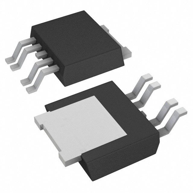
| 供应商器件封装 | DPAK-5 |
| 其它名称 | NCV4276BDT50RKGOSCT |
| 包装 | 剪切带 (CT) |
| 商标 | ON Semiconductor |
| 回动电压—最大值 | 500 mV |
| 安装类型 | 表面贴装 |
| 安装风格 | SMD/SMT |
| 封装 | Reel |
| 封装/外壳 | TO-252-5,DPak(4 引线 + 接片),TO-252AD |
| 封装/箱体 | DPAK-5 |
| 工作温度 | -40°C ~ 150°C |
| 工厂包装数量 | 2500 |
| 最大输入电压 | 45 V |
| 标准包装 | 1 |
| 电压-跌落(典型值) | 0.25V @ 250mA |
| 电压-输入 | 最高 40 V |
| 电压-输出 | 5V |
| 电压调节准确度 | 2 % |
| 电流-输出 | 400mA |
| 电流-限制(最小值) | 400mA |
| 稳压器拓扑 | 正,固定式 |
| 稳压器数 | 1 |
| 系列 | NCV4276B |
| 负载调节 | 20 mV |
| 输出电压 | 5 V |
| 输出电流 | 400 mA |
| 输出类型 | Fixed |


- 商务部:美国ITC正式对集成电路等产品启动337调查
- 曝三星4nm工艺存在良率问题 高通将骁龙8 Gen1或转产台积电
- 太阳诱电将投资9.5亿元在常州建新厂生产MLCC 预计2023年完工
- 英特尔发布欧洲新工厂建设计划 深化IDM 2.0 战略
- 台积电先进制程称霸业界 有大客户加持明年业绩稳了
- 达到5530亿美元!SIA预计今年全球半导体销售额将创下新高
- 英特尔拟将自动驾驶子公司Mobileye上市 估值或超500亿美元
- 三星加码芯片和SET,合并消费电子和移动部门,撤换高东真等 CEO
- 三星电子宣布重大人事变动 还合并消费电子和移动部门
- 海关总署:前11个月进口集成电路产品价值2.52万亿元 增长14.8%


PDF Datasheet 数据手册内容提取
NCV4276B 400 mA Low‐Drop Voltage Regulator The NCV4276B is a 400mA output current integrated low dropout regulator family designed for use in harsh automotive environments. It includes wide operating temperature and input voltage ranges. The http://onsemi.com device is offered with 3.3V, 5.0 V, and adjustable voltage versions available in 2% output voltage accuracy. It has a high peak input voltage tolerance and reverse input voltage protection. It also provides overcurrent protection, overtemperature protection and inhibit for control of the state of the output voltage. The NCV4276B family is available in DPAK and D2PAK surface mount packages. DPAK D2PAK The output is stable over a wide output capacitance and ESR range. CASE 175AA CASE 936A The NCV4276B has improved startup behavior during input voltage transients. MARKING DIAGRAMS Features • 3.3V, 5.0 V, and Adjustable Voltage Version (from 2.5V to 20V) ±2% Output Voltage 76BXXG • 400mA Output Current ALYWW • 500mV (max) Dropout Voltage (5.0V Output) • Inhibit Input 1 • Very Low Current Consumption DPAK • Fault Protection 5-PIN ♦ +45V Peak Transient Voltage ♦ −42V Reverse Voltage ♦ Short Circuit NC ♦ Thermal Overload V4276B−XX • NCV Prefix for Automotive and Other Applications Requiring AWLYWWG Unique Site and Control Change Requirements • These are Pb-Free Devices 1 D2PAK 5-PIN *Tab is connected to Pin 3 on all packages. A = Assembly Location WL, L = Wafer Lot Y = Year WW = Work Week G = Pb-Free Device XX = 33 (3.3V) = 50 (5.0V) = AJ (Adj. Voltage) ORDERING INFORMATION See detailed ordering and shipping information in the ordering information section on page 16 of this data sheet. © Semiconductor Components Industries, LLC, 2014 1 Publication Order Number: August, 2014 − Rev. 6 NCV4276B/D
NCV4276B I Q Error Current Limit and Amplifier Saturation Sense Bandgap − Reference + Thermal Shutdown INH GND NC Figure 1. NCV4276B Block Diagram I Q Error Current Limit and Amplifier Saturation Sense Bandgap − Reference + Thermal Shutdown INH GND VA Figure 2. NCV4276B Adjustable Block Diagram http://onsemi.com 2
NCV4276B Table 1. PIN FUNCTION DESCRIPTION Pin No. Symbol Description 1 I Input; Battery Supply Input Voltage. 2 INH Inhibit; Set low-to inhibit. 3 GND Ground; Pin 3 internally connected to heatsink. 4 NC/VA Not connected for fixed voltage version/Voltage Adjust Input for adjustable voltage version; use an external voltage divider to set the output voltage 5 Q Output: Bypass with a capacitor to GND. See Figures 3 to 7 and Regulator Stability Considerations section. Table 2. MAXIMUM RATINGS* Rating Symbol Min Max Unit Input Voltage VI −42 45 V Input Peak Transient Voltage VI − 45 V Inhibit INH Voltage VINH −42 45 V Voltage Adjust Input VA VVA −0.3 10 V Output Voltage VQ −1.0 40 V Ground Current Iq − 100 mA Input Voltage Operating Range VI VQ + 0.5 V or 4.5 V 40 V (Note 1) ESD Susceptibility (Human Body Model) − 4.0 − kV (Machine Model) − 250 − V (Charged Device Model) − 1.25 − kV Junction Temperature TJ −40 150 °C Storage Temperature Tstg −50 150 °C Stresses exceeding Maximum Ratings may damage the device. Maximum Ratings are stress ratings only. Functional operation above the Recommended Operating Conditions is not implied. Extended exposure to stresses above the Recommended Operating Conditions may affect device reliability. *During the voltage range which exceeds the maximum tested voltage of I, operation is assured, but not specified. Wider limits may apply. Thermal dissipation must be observed closely. 1. Minimum VI = 4.5 V or (VQ + 0.5 V), whichever is higher. Table 3. LEAD TEMPERATURE SOLDERING REFLOW (Note 2) Lead Temperature Soldering TSLD °C Reflow (SMD styles only), Leaded, 60−150 s above 183, 30 s max at peak − 240 Reflow (SMD styles only), Lead Free, 60−150 s above 217, 40 s max at peak − 265 Wave Solder (through hole styles only), 12 sec max − 310 2. Per IPC/JEDEC J−STD−020C. Table 4. THERMAL CHARACTERISTICS (Notes 3 and 4) Characteristic Test Conditions (Typical Value) Unit DPAK 5-PIN PACKAGE Min Pad Board (Note 5) 1(cid:2) Pad Board (Note 6) Junction-to-Tab (psi-JLx, (cid:2)JLx) 4.2 4.7 C/W Junction-to-Ambient (R(cid:3)JA, (cid:3)JA) 100.9 46.8 C/W D2PAK 5-PIN PACKAGE 0.4 sq. in. Spreader Board (Note 7) 1.2 sq. in. Spreader Board (Note 8) Junction-to-Tab (psi-JLx, (cid:2)JLx) 3.8 4.0 C/W Junction-to-Ambient (R(cid:3)JA, (cid:3)JA) 74.8 41.6 C/W 3. Minimum VI = 4.5 V or (VQ + 0.5 V), whichever is higher. 4. Per IPC/JEDEC J−STD−020C. 5. 1 oz. copper, 0.26 inch2 (168 mm2) copper area, 0.062″ thick FR4. 6. 1 oz. copper, 1.14 inch2 (736 mm2) copper area, 0.062″ thick FR4. 7. 1 oz. copper, 0.373 inch2 (241 mm2) copper area, 0.062″ thick FR4. 8. 1 oz. copper, 1.222 inch2 (788 mm2) copper area, 0.062″ thick FR4. http://onsemi.com 3
NCV4276B Table 5. ELECTRICAL CHARACTERISTICS (VI = 13.5 V; −40°C < TJ < 150°C; unless otherwise noted.) NCV4276B Characteristic Symbol Test Conditions Min Typ Max Unit OUTPUT Output Voltage, 5.0 V Version VQ 5.0 mA < IQ < 400 mA, 4.9 5.0 5.1 V 6.0 V < VI < 28 V Output Voltage, 5.0 V Version VQ 5.0 mA < IQ < 200 mA, 4.9 5.0 5.1 V 6.0 V < VI < 40 V Output Voltage, 3.3 V Version VQ 5.0 mA < IQ < 400 mA, 3.234 3.3 3.366 V 4.5 V < VI < 28 V Output Voltage, 3.3 V Version VQ 5.0 mA < IQ < 200 mA, 3.234 3.3 3.366 V 4.5 V < VI < 40 V Output Voltage, Adjustable AVQ 5.0 mA < IQ < 400 mA −2% − +2% V Version VQ+1 < VI < 40 V VI > 4.5 V Output Current Limitation IQ VQ = 90% VQTYP (VQTYP = 2.5 V for ADJ Version) 400 700 1100 mA Quiescent Current (Sleep Mode) Iq VINH = 0 V − − 10 (cid:4)A Iq = II − IQ Quiescent Current, Iq = II − IQ Iq IQ = 1.0 mA − 130 200 (cid:4)A Quiescent Current, Iq = II − IQ Iq IQ = 250 mA − 10 15 mA Quiescent Current, Iq = II − IQ Iq IQ = 400 mA − 25 35 mA Dropout Voltage, VDR IQ = 250 mA, VDR = VI − VQ Adjustable Version VI > 4.5 V − 250 500 mV Dropout Voltage (5.0 V Version) VDR IQ = 250 mA (Note 9) − 250 500 mV Load Regulation (cid:5)VQ,LO IQ = 5.0 mA to 400 mA − 3.0 20 mV Line Regulation (cid:5)VQ (cid:5)VI = 12 V to 32 V, − 4.0 15 mV IQ = 5.0 mA Power Supply Ripple Rejection PSRR fr = 100 Hz, Vr = 0.5 VPP − 70 − dB Temperature Output Voltage Drift dVQ/dT − − 0.5 − mV/K INHIBIT Inhibit Voltage, Output High VINH VQ (cid:2) VQMIN − 2.3 2.8 V Inhibit Voltage, Output Low (Off) VINH VQ (cid:3) 0.1 V 1.8 2.2 − V Input Current IINH VINH = 5.0 V 5.0 10 20 (cid:4)A THERMAL SHUTDOWN Thermal Shutdown Temperature* TSD IQ = 5.0 mA 150 − 210 °C Product parametric performance is indicated in the Electrical Characteristics for the listed test conditions, unless otherwise noted. Product performance may not be indicated by the Electrical Characteristics if operated under different conditions. *Guaranteed by design, not tested in production. 9. Measured when the output voltage VQ has dropped 100 mV from the nominal valued obtained at V = 13.5 V. http://onsemi.com 4
NCV4276B II I 1 5 Q IQ Output 5.5 − 45 V Input CI1 CI2 CQ 1.0 (cid:4)F 100 nF NCV4276B 22 (cid:4)F INH 2 4 NC RL 3 IINH GND Figure 3. Applications Circuit; Fixed Voltage Version VQ = [(R1 + R2) * Vref] / R2 II I 1 5 Q IQ Output Input CI1 CI2 CQ 1.0 (cid:4)F 100 nF 22 (cid:4)F Cb* NCV4276B R1 INH 2 4 VA RL 3 IINH GND R2 Cb* − Required if usage of low ESR output capacitor CQ is demand, see Regulator Stability Considerations section Figure 4. Applications Circuit; Adjustable Voltage Version http://onsemi.com 5
NCV4276B TYPICAL PERFORMANCE CHARACTERISTICS 10 CQ = 22 (cid:4)F for all Unstable Region Fixed Output Voltages 1 (cid:6)) R ( Maximum ESR ES Stable Region for CQ = 22 (cid:4)F 0.1 0.01 0 50 100 150 200 250 300 350 400 IQ, OUTPUT CURRENT (mA) Figure 5. Output Stability with Output Capacitor ESR, 5.0 V and 3.3 V Regulator 10 CQ = 10 (cid:4)F for 3.3 V and Unstable Region 5 V Fixed Output Voltages 1 (cid:6)) R ( Maximum ESR ES Stable Region for CQ = 10 (cid:4)F 0.1 0.01 0 50 100 150 200 250 300 350 400 IQ, OUTPUT CURRENT (mA) Figure 6. Output Stability with Output Capacitor ESR, 5.0 V and 3.3 V Regulator 100 CQ = 22 (cid:4)F for these Unstable Region Output Voltages 10 (cid:6)) 12 V R ( 1 Stable Region 2.5 V 6 V S E 0.1 Unstable Region Cb capacitor not connected 0.01 0 50 100 150 200 250 300 350 400 IQ, OUTPUT CURRENT (mA) Figure 7. Output Stability with Output Capacitor ESR, Adjustable Regulator http://onsemi.com 6
NCV4276B TYPICAL PERFORMANCE CHARACTERISTICS − 4276B Version 5.2 3.45 VI = 13.5 V E (V) 5.1 RL = 1 k(cid:6) E (V) 3.40 VRI L= = 1 13 .k5(cid:6) V G G A A 3.35 T T L L O O V V T 5.0 T 3.30 U U P P T T U U 3.25 O O , Q 4.9 , Q V V 3.20 4.8 3.15 −40 0 40 80 120 160 −40 0 40 80 120 160 TJ, JUNCTION TEMPERATURE (°C) TJ, JUNCTION TEMPERATURE (°C) Figure 8. Output Voltage vs. Figure 9. Output Voltage vs. Junction Temperature, 5.0 V Version Junction Temperature, 3.3 V Version 40 10 N (mA) RTJL == 2250° (cid:6)C N (mA) 89..00 RTJL == 2250° (cid:6)C O 30 O PTI PTI 7.0 UM UM 6.0 S S N 20 N 5.0 O O NT C NT C 4.0 E E 3.0 URR 10 URR 2.0 C C I, q 0 I, q 1.00 0 10 20 30 40 50 0 10 20 30 40 50 VI, INPUT VOLTAGE (V) VI, INPUT VOLTAGE (V) Figure 10. Current Consumption vs. Figure 11. Current Consumption vs. Input Input Voltage, 5.0 V Version Voltage, 3.3 V Version 6.0 6.0 E (V) 5.0 E (V) 5.0 RTJL == 2250° (cid:6)C OLTAG 4.0 RTJL == 2250° (cid:6)C OLTAG 4.0 UT V 3.0 UT V 3.0 P P UT 2.0 UT 2.0 O O V, Q 1.0 V, Q 1.0 0 0 0 2.0 4.0 6.0 8.0 10 0 1.0 2.0 3.0 4.0 5.0 6.0 VI, INPUT VOLTAGE (V) VI, INPUT VOLTAGE (V) Figure 12. Low Voltage Behavior, 5.0 V Version Figure 13. Low Voltage Behavior, 3.3 V Version http://onsemi.com 7
NCV4276B TYPICAL PERFORMANCE CHARACTERISTICS − 4276B Version 6.0 2.0 4.0 A) A) 0 m 2.0 m T ( T ( −2.0 N 0 N E E R R R R U −2.0 U −4.0 C C T T U −4.0 U P P −6.0 N N I, II−−86..00 RTLJ = = 6 2.85 °kC(cid:6) I, II−8.0 RTLJ = = 6 2.85 °kC(cid:6) −10 −10 −50 −25 0 25 50 −50 −25 0 25 50 VI, INPUT VOLTAGE (V) VI, INPUT VOLTAGE (V) Figure 14. Input Current vs. Input Voltage, Figure 15. Input Current vs. Input Voltage, 5.0 V Version 3.3V Version 600 800 TJ = 25°C V) 500 mA) VQ = 0 V E (m TJ = 125°C NT ( 600 G 400 E A R T R VOL 300 CU 400 OP TJ = 25°C UT R 200 TP D U , R O 200 VD 100 I, Q 0 0 0 100 200 300 400 0 10 20 30 40 50 IQ, OUTPUT CURRENT (mA) VI, INPUT VOLTAGE (V) Figure 16. Dropout Voltage vs. Figure 17. Maximum Output Current vs. Output Current Input Voltage 60 1.6 A) A) m m 1.4 ON ( 50 ON ( 1.2 VI = 13.5 V MPTI 40 VTIJ = = 1 235.5°C V MPTI 1.0 TJ = 25°C U U S S N 30 N 0.8 O O C C T T 0.6 N 20 N E E R R 0.4 R R U 10 U C C 0.2 I, q 0 I, q 0 0 100 200 300 400 500 600 0 10 20 30 40 50 60 IQ, OUTPUT CURRENT (mA) IQ, OUTPUT CURRENT (mA) Figure 18. Current Consumption vs. Figure 19. Current Consumption vs. Output Current (High Load) Output Current (Low Load) http://onsemi.com 8
NCV4276B TYPICAL PERFORMANCE CHARACTERISTICS − Adjustable Version 2.55 5.0 E (V)22..5534 VTIJ = = 1 235.5°C V N (mA) 44..05 RTJL == 2250° (cid:6)C G O A2.52 TI 3.5 T P VOL2.51 UM 3.0 T 2.50 NS 2.5 U O UTP2.49 T C 2.0 O N , Q2.48 RE 1.5 V2.47 UR 1.0 C 2.46 , q 0.5 I 2.45 0 −40 0 40 80 120 160 0 10 20 30 40 50 TJ, JUNCTION TEMPERATURE (°C) VI, INPUT VOLTAGE (V) Figure 20. Output Voltage vs. Junction Figure 21. Current Consumption vs. Input Temperature, Adjustable Version Voltage, Adjustable Version 4 2 TAGE (V) 3.53 RTJL == 2250° (cid:6)C NT (mA) −−420 L 2.5 E O R −6 V R T 2 U −8 U C UTP 1.5 PUT −10 O N−12 V, Q 1 I, II−14 TJ = 25°C 0.5 RL = 6.8 k(cid:6) −16 0 −18 0 2 4 6 8 10 −50 −25 0 25 50 VI, INPUT VOLTAGE (V) VI, INPUT VOLTAGE (V) Figure 22. Low Voltage Behavior, Figure 23. High Voltage Behavior, Adjustable Version Adjustable Version http://onsemi.com 9
NCV4276B TYPICAL PERFORMANCE CHARACTERISTICS − Adjustable Version 600 800 mV) A) 700 GE ( 500 T (m 600 OLTA 400 TJ = 125°C RREN 500 POUT V 300 TJ = 25°C PUT CU 400 TVJQ = = 2 05 °VC O T 300 R 200 U D O , R , Q200 D 100 I V 100 0 0 0 50 100 150 200 250 300 350 400 0 10 20 30 40 50 IQ, OUTPUT CURRENT (mA) VI, INPUT VOLTAGE (V) Figure 24. Dropout Voltage vs. Output Current, Figure 25. Maximum Output Current vs. Regulator Set at 5.0 V, Adjustable Version Input Voltage, Adjustable Version 60 1.6 mA) TJ = 25°C mA) 1.4 TJ = 25°C N ( 50 VI = 13.5 V N ( VI = 13.5 V O O 1.2 TI TI P 40 P M M 1.0 U U S S N 30 N 0.8 O O C C T T 0.6 N 20 N E E R R 0.4 R R U 10 U C C 0.2 , q , q I I 0 0 0 100 200 300 400 500 600 0 10 20 30 40 50 60 IQ, OUTPUT CURRENT (mA) IQ, OUTPUT CURRENT (mA) Figure 26. Current Consumption vs. Figure 27. Current Consumption vs. Output Output Current (High Load), Adjustable Version Current (Low Load), Adjustable Version http://onsemi.com 10
NCV4276B Circuit Description Minimum ESR for C =22(cid:4)F is native ESR of ceramic Q The NCV4276B is an integrated low dropout regulator capacitor with which the fixed output voltage devices are that provides a regulated voltage at 400 mA to the output. performing stable. Murata ceramic capacitors were used, It is enabled with an input to the inhibit pin. The regulator GRM32ER71C226KE18 (22(cid:4)F, 16V, X7R, 1210), voltage is provided by a PNP pass transistor controlled by GRM31CR71C106KAC7 (10(cid:4)F, 16V, X7R, 1206). an error amplifier with a bandgap reference, which gives it the lowest possible dropout voltage. The output current Calculating Bypass Capacitor capability is 400 mA, and the base drive quiescent current If usage of low ESR ceramic capacitors is demand in case is controlled to prevent oversaturation when the input of Adjustable Regulator, connect the bypass capacitor C b voltage is low or when the output is overloaded. The between Voltage Adjust pin and Q pin according to regulator is protected by both current limit and thermal Applications circuit at Figure4. shutdown. Thermal shutdown occurs above 150°C to Parallel combination of bypass capacitor C with the b protect the IC during overloads and extreme ambient feedback resistor R contributes in the device transfer 1 temperatures. function as an additional zero and affects the device loop stability, therefore its value must be optimized. Attention Regulator to the Output Capacitor value and its ESR must be paid. See The error amplifier compares the reference voltage to a also Stability in High Speed Linear LDO Regulators sample of the output voltage (V ) and drives the base of a Q Application Note, AND8037/D for more information. PNP series pass transistor via a buffer. The reference is a Optimal value of bypass capacitor is given by following bandgap design to give it a temperature-stable output. expression Saturation control of the PNP is a function of the load cpuorwreenr t daenvdic ein ipsu tp rveovletnagteed. , Oanvder sqautuiersactieonnt couf rrtehnet oinu tpthuet Cb(cid:4)2(cid:5)(cid:2)(cid:5)1fz(cid:5)R1(cid:6)(F) (eq. 1) ground pin is minimized. See Figure 4, Test Circuit, for where circuit element nomenclature illustration. R = the upper feedback resistor 1 f = the frequency of the zero added into the device z Regulator Stability Considerations transfer function by R and C external components. 1 b The input capacitors (C and C ) are necessary to I1 I2 stabilize the input impedance to avoid voltage line Set the R1 resistor according to output voltage influences. Using a resistor of approximately 1.0 (cid:6) in requirement. Chose the fz with regard on the output series with CI2 can stop potential oscillations caused by capacitance CQ, refer to the table below. stray inductance and capacitance. The output capacitor helps determine three main CQ ((cid:2)F) 10 22 47 100 characteristics of a linear regulator: startup delay, load fz Range (kHz) 20 - 50 14 - 35 10 - 20 7 – 14 transient response and loop stability. The capacitor value Ceramic capacitors and its part numbers listed bellow and type should be based on cost, availability, size and have been used as low ESR output capacitors C from the temperature constraints. The aluminum electrolytic Q table above to define the frequency ranges of additional capacitor is the least expensive solution, but, if the circuit zero required for stability. operates at low temperatures (−25°C to −40°C), both the value and ESR of the capacitor will vary considerably. The GRM31CR71C106KAC7 (10(cid:4)F, 16V, X7R, 1206) capacitor manufacturer’s data sheet usually provides this GRM32ER71C226KE18 (22(cid:4)F, 16V, X7R, 1210) information. GRM32ER61C476ME15 (47(cid:4)F, 16V, X5R, 1210) The value for the output capacitor C , shown in Figure 3, Q GRM32ER60J107ME20 (100(cid:4)F, 6.3V, X5R, 1210) should work for most applications; see also Figures5 to 7 for output stability at various load and Output Capacitor Inhibit Input ESR conditions. Stable region of ESR in Figures5 to 7 The inhibit pin is used to turn the regulator on or off. By shows ESR values at which the LDO output voltage does holding the pin down to a voltage less than 1.8V, the output not have any permanent oscillations at any dynamic of the regulator will be turned off. When the voltage on the changes of output load current. Marginal ESR is the value Inhibit pin is greater than 2.8V, the output of the regulator at which the output voltage waving is fully damped during will be enabled to power its output to the regulated output four periods after the load change and no oscillation is voltage. The inhibit pin may be connected directly to the further observable. input pin to give constant enable to the output regulator. ESR characteristics were measured with ceramic capacitors and additional series resistors to emulate ESR. Setting the Output Voltage (Adjustable Version) Low duty cycle pulse load current technique has been used The output voltage range of the adjustable version can be to maintain junction temperature close to ambient set between 2.5V and 20V. This is accomplished with an temperature. external resistor divider feeding back the voltage to the IC http://onsemi.com 11
NCV4276B back to the error amplifier by the voltage adjust pin VA. II IQ The internal reference voltage is set to a temperature stable VI SMART VQ reference of 2.5V. REGULATOR The output voltage is calculated from the following Control formula. Ignoring the bias current into the VA pin: Features VQ(cid:4)[(R1(cid:7)R2) * Vref](cid:8)R2 (eq. 2) Iq Use R2<50k to avoid significant voltage output errors due to VA bias current. Connecting VA directly to Q without R1 and R2 creates Figure 28. Single Output Regulator with Key an output voltage of 2.5V. Performance Parameters Labeled Designers should consider the tolerance of R1 and R2 during the design phase. Heatsinks The input voltage range for operation (pin1) of the A heatsink effectively increases the surface area of the adjustable version is between (VQ+0.5V) and 40V. package to improve the flow of heat away from the IC and Internal bias requirements dictate a minimum input voltage into the surrounding air. of 4.5V. The dropout voltage for output voltages less than Each material in the heat flow path between the IC and 4.0V is (4.5V−VQ). the outside environment will have a thermal resistance. Like series electrical resistances, these resistances are Calculating Power Dissipation in a Single Output Linear Regulator summed to determine the value of R(cid:3)JA: The maximum power dissipation for a single output R(cid:3)JA(cid:4)R(cid:3)JC(cid:7)R(cid:3)CS(cid:7)R(cid:3)SA (eq. 5) regulator (Figure28) is: where: PD(max)(cid:4)[VI(max)(cid:9)VQ(min)]IQ(max)(cid:7) (eq. 3) R(cid:3)JC is the junction-to-case thermal resistance, (cid:7)VI(max)Iq R(cid:3)CS is the case-to-heatsink thermal resistance, where: R(cid:3)SA is the heatsink-to-ambient thermal resistance. VI(max) is the maximum input voltage, R(cid:3)JC appears in the package section of the data sheet. VQ(min) is the minimum output voltage, Like R(cid:3)JA, it too is a function of package type. R(cid:3)CS and IQ(max) is the maximum output current for the R(cid:3)SA are functions of the package type, heatsink and the application, interface between them. These values appear in data sheets I is the quiescent current the regulator of heatsink manufacturers. q consumes at I . Thermal, mounting, and heatsinking considerations are Q(max) discussed in the ON Semiconductor application note Once the value of P is known, the maximum D(max) AN1040/D. permissible value of R(cid:3)JA can be calculated: R(cid:3)JA(cid:4)150oC(cid:9)TA (eq. 4) Thermal Model PD See pages 13 to 16 for detailed information about thermal The value of R(cid:3)JA can then be compared with those in the model parameters. package section of the data sheet. Those packages with R(cid:3)JA less than the calculated value in Equation4 will keep the die temperature below 150°C. In some cases, none of the packages will be sufficient to dissipate the heat generated by the IC, and an external heatsink will be required. http://onsemi.com 12
NCV4276B Table 6. DPAK 5-LEAD THERMAL RC NETWORK MODELS Drain Copper Area (1 oz thick) 168 mm2 736 mm2 168 mm2 736 mm2 (SPICE Deck Format) Cauer Network Foster Network 168 mm2 736 mm2 Units Tau Tau Units C_C1 Junction GND 1.00E−06 1.00E−06 W−s/C 1.36E−08 1.361E−08 sec C_C2 node1 GND 1.00E−05 1.00E−05 W−s/C 7.41E−07 7.411E−07 sec C_C3 node2 GND 6.00E−05 6.00E−05 W−s/C 1.04E−05 1.029E−05 sec C_C4 node3 GND 1.00E−04 1.00E−04 W−s/C 3.91E−05 3.737E−05 sec C_C5 node4 GND 4.36E−04 3.64E−04 W−s/C 1.80E−03 1.376E−03 sec C_C6 node5 GND 6.77E−02 1.92E−02 W−s/C 3.77E−01 2.851E−02 sec C_C7 node6 GND 1.51E−01 1.27E−01 W−s/C 3.79E+00 9.475E−01 sec C_C8 node7 GND 4.80E−01 1.018 W−s/C 2.65E+01 1.173E+01 sec C_C9 node8 GND 3.740 2.955 W−s/C 8.71E+01 8.59E+01 sec C_C10 node9 GND 10.322 0.438 W−s/C sec 168 mm2 736 mm2 R’s R’s R_R1 Junction node1 0.015 0.015 C/W 0.0123 0.0123 C/W R_R2 node1 node2 0.08 0.08 C/W 0.0585 0.0585 C/W R_R3 node2 node3 0.4 0.4 C/W 0.0304 0.0287 C/W R_R4 node3 node4 0.2 0.2 C/W 0.3997 0.3772 C/W R_R5 node4 node5 2.97519 2.6171 C/W 3.115 2.68 C/W R_R6 node5 node6 8.2971 1.6778 C/W 3.571 1.38 C/W R_R7 node6 node7 25.9805 7.4246 C/W 12.851 5.92 C/W R_R8 node7 node8 46.5192 14.9320 C/W 35.471 7.39 C/W R_R9 node8 node9 17.7808 19.2560 C/W 46.741 28.94 C/W R_R10 node9 GND 0.1 0.1758 C/W C/W NOTE: Bold face items represent the package without the external thermal system. Junction R1 R2 R3 Rn C1 C2 C3 Cn Time constants are not simple RC products. Amplitudes Ambient of mathematical solution are not the resistance values. (thermal ground) Figure 29. Grounded Capacitor Thermal Network (“Cauer” Ladder) Junction R1 R2 R3 Rn C1 C2 C3 Cn Each rung is exactly characterized by its RC-product Ambient time constant; amplitudes are the resistances. (thermal ground) Figure 30. Non-Grounded Capacitor Thermal Ladder (“Foster” Ladder) http://onsemi.com 13
NCV4276B Table 7. D2PAK 5-LEAD THERMAL RC NETWORK MODELS Drain Copper Area (1 oz thick) 241 mm2 788 mm2 241 mm2 788 mm2 (SPICE Deck Format) Cauer Network Foster Network 241 mm2 653 mm2 Units Tau Tau Units C_C1 Junction GND 1.00E−06 1.00E−06 W−s/C 1.361E−08 1.361E−08 sec C_C2 node1 GND 1.00E−05 1.00E−05 W−s/C 7.411E−07 7.411E−07 sec C_C3 node2 GND 6.00E−05 6.00E−05 W−s/C 1.005E−05 1.007E−05 sec C_C4 node3 GND 1.00E−04 1.00E−04 W−s/C 3.460E−05 3.480E−05 sec C_C5 node4 GND 2.82E−04 2.87E−04 W−s/C 7.868E−04 8.107E−04 sec C_C6 node5 GND 5.58E−03 5.95E−03 W−s/C 7.431E−03 7.830E−03 sec C_C7 node6 GND 4.25E−01 4.61E−01 W−s/C 2.786E+00 2.012E+00 sec C_C8 node7 GND 9.22E−01 2.05 W−s/C 2.014E+01 2.601E+01 sec C_C9 node8 GND 1.73 4.88 W−s/C 1.134E+02 1.218E+02 sec C_C10 node9 GND 7.12 1.31 W−s/C sec 241 mm2 653 mm2 R’s R’s R_R1 Junction node1 0.015 0.0150 C/W 0.0123 0.0123 C/W R_R2 node1 node2 0.08 0.0800 C/W 0.0585 0.0585 C/W R_R3 node2 node3 0.4 0.4000 C/W 0.0257 0.0260 C/W R_R4 node3 node4 0.2 0.2000 C/W 0.3413 0.3438 C/W R_R5 node4 node5 1.85638 1.8839 C/W 1.77 1.81 C/W R_R6 node5 node6 1.23672 1.2272 C/W 1.54 1.52 C/W R_R7 node6 node7 9.81541 5.3383 C/W 4.13 3.46 C/W R_R8 node7 node8 33.1868 18.9591 C/W 6.27 5.03 C/W R_R9 node8 node9 27.0263 13.3369 C/W 60.80 29.30 C/W R_R10 node9 GND 1.13944 0.1191 C/W C/W NOTE: Bold face items represent the package without the external thermal system. The Cauer networks generally have physical simulating tools, whereas Foster networks may be more significance and may be divided between nodes to separate easily implemented using mathematical tools (for instance, thermal behavior due to one portion of the network from in a spreadsheet program), according to the following another. The Foster networks, though when sorted by time formula: constant (as above) bear a rough correlation with the Cauer n (cid:4) networks, are really only convenient mathematical models. R(t)(cid:4) Ri(cid:10)1−e−t(cid:8)taui (cid:11) (eq. 6) Cauer networks can be easily implemented using circuit i(cid:4)1 http://onsemi.com 14
NCV4276B 110 110 100 100 90 90 W) 80 W) 80 °/ °/ C 70 C 70 A ( 1 oz A ( 1 oz J J (cid:3) 60 (cid:3) 60 2 oz 2 oz 50 50 40 40 30 30 150 200 250 300350 400 450 500550 600 650700 750 150 200 250 300350 400 450 500550 600 650700 750 COPPER AREA (mm2) COPPER AREA (mm2) Figure 31. (cid:3)JA vs. Copper Spreader Area, Figure 32. (cid:3)JA vs. Copper Spreader Area, DPAK 5-Lead D2PAK 5-Lead 100 Cu Area 167 mm2 10 Cu Area 736 mm2 W °/ C 1.0 R(t) sqrt(t) 0.1 0.01 0.0000001 0.000001 0.00001 0.0001 0.001 0.01 0.1 1.0 10 100 1000 TIME (sec) Figure 33. Single-Pulse Heating Curves, DPAK 5-Lead 100 Cu Area 167 mm2 10 Cu Area 736 mm2 W °/ C 1.0 R(t) 0.1 0.01 0.0000001 0.000001 0.00001 0.0001 0.001 0.01 0.1 1.0 10 100 1000 TIME (sec) Figure 34. Single-Pulse Heating Curves, D2PAK 5-Lead http://onsemi.com 15
NCV4276B 100 50% Duty Cycle 20% 10 W 10% °/ C 5% 2 m 2% m 1.0 6 1% 3 7 A J (cid:3) R 0.1 Non−normalized Response 0.01 0.0000001 0.000001 0.00001 0.0001 0.001 0.01 0.1 1.0 10 100 1000 PULSE WIDTH (sec) Figure 35. Duty Cycle for 1(cid:2) Spreader Boards, DPAK 5-Lead 100 50% Duty Cycle 20% 10 W 10% °/ C 2 5% m m 1.0 2% 8 1% 8 7 A J (cid:3) R 0.1 Non−normalized Response 0.01 0.0000001 0.000001 0.00001 0.0001 0.001 0.01 0.1 1.0 10 100 1000 PULSE WIDTH (sec) Figure 36. Duty Cycle for 1(cid:2) Spreader Boards, D2PAK 5-Lead Table 8. ORDERING INFORMATION Device Output Voltage Accuracy Output Voltage Package Shipping† NCV4276BDT33RKG DPAK, 5-Pin 2,500 / Tape & Reel (Pb-Free) 3.3 V NCV4276BDS33R4G D2PAK, 5-Pin 800 / Tape & Reel (Pb-Free) NCV4276BDT50RKG DPAK, 5-Pin 2,500 / Tape & Reel (Pb-Free) 2% 5.0 V NCV4276BDS50R4G D2PAK, 5-Pin 800 / Tape & Reel (Pb-Free) NCV4276BDTADJRKG DPAK, 5-Pin 2,500 / Tape & Reel (Pb-Free) Adjustable NCV4276BDSADJR4G D2PAK, 5-Pin 800 / Tape & Reel (Pb-Free) †For information on tape and reel specifications, including part orientation and tape sizes, please refer to our Tape and Reel Packaging Specifications Brochure, BRD8011/D. http://onsemi.com 16
NCV4276B PACKAGE DIMENSIONS DPAK−5, CENTER LEAD CROP CASE 175AA ISSUE B NOTES: −T− SPELAATNIENG 1.DIMENSIONING AND TOLERANCING PER ANSI Y14.5M, 1982. B C 2.CONTROLLING DIMENSION: INCH. V R E R1 INCHES MILLIMETERS DIM MIN MAX MIN MAX A 0.235 0.245 5.97 6.22 B 0.250 0.265 6.35 6.73 C 0.086 0.094 2.19 2.38 Z A D 0.020 0.028 0.51 0.71 S E 0.018 0.023 0.46 0.58 12 3 4 5 F 0.024 0.032 0.61 0.81 U G 0.180 BSC 4.56 BSC K H 0.034 0.040 0.87 1.01 J 0.018 0.023 0.46 0.58 F K 0.102 0.114 2.60 2.89 J L 0.045 BSC 1.14 BSC R 0.170 0.190 4.32 4.83 L H R1 0.185 0.210 4.70 5.33 S 0.025 0.040 0.63 1.01 D5 PL U 0.020 −−− 0.51 −−− V 0.035 0.050 0.89 1.27 G 0.13 (0.005) M T Z 0.155 0.170 3.93 4.32 RECOMMENDED SOLDERING FOOTPRINT* 6.4 0.252 2.2 0.086 5.8 0.34 5.36 0.228 0.013 0.217 10.6 0.8 0.417 0.031 (cid:10) (cid:11) mm SCALE 4:1 inches *For additional information on our Pb−Free strategy and soldering details, please download the ON Semiconductor Soldering and Mounting Techniques Reference Manual, SOLDERRM/D. http://onsemi.com 17
NCV4276B PACKAGE DIMENSIONS D2PAK 5 CASE 936A−02 ISSUE C NOTES: 1. DIMENSIONING AND TOLERANCING PER ANSI Y14.5M, 1982. −T− TERMINAL 6 2. CONTROLLING DIMENSION: INCH. A OCHPATIMOFNEARL E U 3. TAANBD CKO.NTOUR OPTIONAL WITHIN DIMENSIONS A 4. DIMENSIONS U AND V ESTABLISH A MINIMUM MOUNTING SURFACE FOR TERMINAL 6. K S 5. DIMENSIONS A AND B DO NOT INCLUDE MOLD V FLASH OR GATE PROTRUSIONS. MOLD FLASH B AND GATE PROTRUSIONS NOT TO EXCEED 0.025 H (0.635) MAXIMUM. 1 2 3 4 5 M INCHES MILLIMETERS L DIM MIN MAX MIN MAX A 0.386 0.403 9.804 10.236 D B 0.356 0.368 9.042 9.347 N P C 0.170 0.180 4.318 4.572 0.010 (0.254) M T G R D 0.026 0.036 0.660 0.914 E 0.045 0.055 1.143 1.397 G 0.067 BSC 1.702 BSC H 0.539 0.579 13.691 14.707 K 0.050 REF 1.270 REF L 0.000 0.010 0.000 0.254 M 0.088 0.102 2.235 2.591 C N 0.018 0.026 0.457 0.660 P 0.058 0.078 1.473 1.981 R 5 (cid:2) REF 5 (cid:2) REF S 0.116 REF 2.946 REF U 0.200 MIN 5.080 MIN V 0.250 MIN 6.350 MIN SOLDERING FOOTPRINT 8.38 0.33 1.702 0.067 10.66 0.42 1.016 3.05 0.04 0.12 16.02 0.63 (cid:10) (cid:11) mm SCALE 3:1 inches ON Semiconductor and the are registered trademarks of Semiconductor Components Industries, LLC (SCILLC) or its subsidiaries in the United States and/or other countries. SCILLC owns the rights to a number of patents, trademarks, copyrights, trade secrets, and other intellectual property. A listing of SCILLC’s product/patent coverage may be accessed at www.onsemi.com/site/pdf/Patent−Marking.pdf. SCILLC reserves the right to make changes without further notice to any products herein. SCILLC makes no warranty, representation or guarantee regarding the suitability of its products for any particular purpose, nor does SCILLC assume any liability arising out of the application or use of any product or circuit, and specifically disclaims any and all liability, including without limitation special, consequential or incidental damages. “Typical” parameters which may be provided in SCILLC data sheets and/or specifications can and do vary in different applications and actual performance may vary over time. All operating parameters, including “Typicals” must be validated for each customer application by customer’s technical experts. SCILLC does not convey any license under its patent rights nor the rights of others. SCILLC products are not designed, intended, or authorized for use as components in systems intended for surgical implant into the body, or other applications intended to support or sustain life, or for any other application in which the failure of the SCILLC product could create a situation where personal injury or death may occur. Should Buyer purchase or use SCILLC products for any such unintended or unauthorized application, Buyer shall indemnify and hold SCILLC and its officers, employees, subsidiaries, affiliates, and distributors harmless against all claims, costs, damages, and expenses, and reasonable attorney fees arising out of, directly or indirectly, any claim of personal injury or death associated with such unintended or unauthorized use, even if such claim alleges that SCILLC was negligent regarding the design or manufacture of the part. SCILLC is an Equal Opportunity/Affirmative Action Employer. This literature is subject to all applicable copyright laws and is not for resale in any manner. PUBLICATION ORDERING INFORMATION LITERATURE FULFILLMENT: N. American Technical Support: 800−282−9855 Toll Free ON Semiconductor Website: www.onsemi.com Literature Distribution Center for ON Semiconductor USA/Canada P.O. Box 5163, Denver, Colorado 80217 USA Europe, Middle East and Africa Technical Support: Order Literature: http://www.onsemi.com/orderlit Phone: 303−675−2175 or 800−344−3860 Toll Free USA/Canada Phone: 421 33 790 2910 Fax: 303−675−2176 or 800−344−3867 Toll Free USA/Canada Japan Customer Focus Center For additional information, please contact your local Email: orderlit@onsemi.com Phone: 81−3−5817−1050 Sales Representative http://onsemi.com NCV4276B/D 18
Mouser Electronics Authorized Distributor Click to View Pricing, Inventory, Delivery & Lifecycle Information: O N Semiconductor: NCV4276BDTADJRKG NCV4276BDSADJR4G NCV4276BDT50RKG NCV4276BDS50R4G NCV4276BDS33R4G NCV4276BDT33RKG