ICGOO在线商城 > 集成电路(IC) > PMIC - 稳压器 - 线性 > ADP3300ARTZ-5REEL7
 Datasheet下载
- 型号: ADP3300ARTZ-5REEL7
- 制造商: Analog
- 库位|库存: xxxx|xxxx
- 要求:
| 数量阶梯 | 香港交货 | 国内含税 |
| +xxxx | $xxxx | ¥xxxx |
查看当月历史价格
查看今年历史价格
ADP3300ARTZ-5REEL7产品简介:
ICGOO电子元器件商城为您提供ADP3300ARTZ-5REEL7由Analog设计生产,在icgoo商城现货销售,并且可以通过原厂、代理商等渠道进行代购。 ADP3300ARTZ-5REEL7价格参考¥5.87-¥10.20。AnalogADP3300ARTZ-5REEL7封装/规格:PMIC - 稳压器 - 线性, Linear Voltage Regulator IC Positive Fixed 1 Output 5V 50mA SOT-23-6。您可以下载ADP3300ARTZ-5REEL7参考资料、Datasheet数据手册功能说明书,资料中有ADP3300ARTZ-5REEL7 详细功能的应用电路图电压和使用方法及教程。
ADP3300ARTZ-5REEL7 是 Analog Devices Inc. 生产的一款 PMIC(电源管理集成电路)中的线性稳压器。其应用场景主要包括以下几方面:

 1. 低功耗设备
ADP3300ARTZ-5REEL7 具有低静态电流和高精度输出电压的特点,非常适合用于低功耗设备,如便携式电子设备、电池供电系统(例如手持终端、无线传感器节点等)。它能够高效地将输入电压转换为稳定的输出电压,延长电池使用寿命。

 2. 消费类电子产品
该器件适用于各种消费类电子产品,如智能手机、平板电脑、可穿戴设备(如智能手表、健康监测设备)以及音频设备。其小尺寸封装和高集成度使其成为紧凑型设计的理想选择。

 3. 工业自动化
在工业领域,ADP3300ARTZ-5REEL7 可用于为微控制器、传感器接口电路和其他低功耗模块供电。它的稳定性确保了工业设备在恶劣环境下的可靠运行,例如数据采集系统、过程控制单元和远程监控装置。

 4. 通信设备
该线性稳压器适合应用于通信设备中,例如路由器、调制解调器、基站的辅助电源部分。它能够为射频模块、信号处理芯片提供稳定且低噪声的电源,从而提高通信质量。

 5. 汽车电子
尽管 ADP3300ARTZ-5REEL7 不是专门针对汽车级应用设计的产品,但在某些非关键车载子系统中仍可使用,比如信息娱乐系统、导航设备或车内环境控制系统。它能为这些系统的 MCU 和传感器提供稳定的电源支持。

 6. 医疗设备
对于需要高精度和低噪声电源的医疗设备来说,这款稳压器非常适用。例如,在血糖仪、脉搏血氧仪或其他便携式医疗仪器中,它可以为敏感的模拟前端电路提供清洁的电源。

 总结
ADP3300ARTZ-5REEL7 的主要优势在于其简单易用、高效率以及出色的性能表现,因此广泛应用于对电源要求较高但又追求小型化和低成本的设计场景中。无论是消费类电子产品还是工业级解决方案,这款线性稳压器都能提供可靠的电源支持。
| 参数 | 数值 |
| 产品目录 | 集成电路 (IC)半导体 |
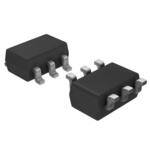
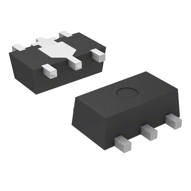
| 描述 | IC REG LDO 5V 50MA SOT23-6线性稳压器 High Acc 50mA LDO |
| 产品分类 | |
| 品牌 | Analog Devices |
| 产品手册 | |
| 产品图片 |
|
| rohs | 符合RoHS无铅 / 符合限制有害物质指令(RoHS)规范要求 |
| 产品系列 | 电源管理 IC,线性稳压器,Analog Devices ADP3300ARTZ-5REEL7anyCAP® |
| 数据手册 | |
| 产品型号 | ADP3300ARTZ-5REEL7 |
| 产品目录页面 | |
| 产品种类 | |
| 供应商器件封装 | SOT-23-6 |
| 其它名称 | ADP3300ARTZ-5REEL7TR |
| 包装 | 带卷 (TR) |
| 商标 | Analog Devices |
| 安装类型 | 表面贴装 |
| 安装风格 | SMD/SMT |
| 封装 | Reel |
| 封装/外壳 | SOT-23-6 |
| 封装/箱体 | SOT-23-6 |
| 工作温度 | -40°C ~ 85°C |
| 工厂包装数量 | 3000 |
| 最大输入电压 | 12 V |
| 最小输入电压 | 3 V |
| 标准包装 | 3,000 |
| 电压-跌落(典型值) | 0.08V @ 50mA |
| 电压-输入 | 最高 12V |
| 电压-输出 | 5V |
| 电流-输出 | 50mA |
| 电流-限制(最小值) | - |
| 稳压器拓扑 | 正,固定式 |
| 稳压器数 | 1 |
| 系列 | ADP3300 |
| 视频文件 | http://www.digikey.cn/classic/video.aspx?PlayerID=1364138032001&width=640&height=505&videoID=2245193149001 |
| 负载调节 | 0.06 mV |
| 输出电流 | 50 mA |


- 商务部:美国ITC正式对集成电路等产品启动337调查
- 曝三星4nm工艺存在良率问题 高通将骁龙8 Gen1或转产台积电
- 太阳诱电将投资9.5亿元在常州建新厂生产MLCC 预计2023年完工
- 英特尔发布欧洲新工厂建设计划 深化IDM 2.0 战略
- 台积电先进制程称霸业界 有大客户加持明年业绩稳了
- 达到5530亿美元!SIA预计今年全球半导体销售额将创下新高
- 英特尔拟将自动驾驶子公司Mobileye上市 估值或超500亿美元
- 三星加码芯片和SET,合并消费电子和移动部门,撤换高东真等 CEO
- 三星电子宣布重大人事变动 还合并消费电子和移动部门
- 海关总署:前11个月进口集成电路产品价值2.52万亿元 增长14.8%


PDF Datasheet 数据手册内容提取
a High Accuracy anyCAP® 50 mA Low Dropout Linear Regulator ADP3300 FEATURES FUNCTIONAL BLOCK DIAGRAM High Accuracy Over Line and Load: (cid:1)0.8% @ 25(cid:2)C, (cid:1)1.4% Over Temperature ADP3300 Ultralow Dropout Voltage: 80 mV Typical @ 50 mA IN Q1 OUT Requires Only C = 0.47 (cid:3)F for Stability O anyCAP = Stable with All Types of Capacitors THERMAL CC R1 ERR PROTECTION (Including MLCC) Current and Thermal Limiting Q2 DRIVER gm Low Noise SD R2 + Dropout Detector BANDGAP REF – Low Shutdown Current: 1 (cid:3)A 3.0 V to 12 V Supply Range GND –40(cid:2)C to +85(cid:2)C Ambient Temperature Range Several Fixed Voltage Options Ultrasmall SOT-23 6-Lead Package Excellent Line and Load Regulation APPLICATIONS Cellular Telephones Notebook, Palmtop Computers Battery Powered Systems PCMCIA Regulators Bar Code Scanners Camcorders, Cameras NR ADP3300-5 GENERAL DESCRIPTION VIN + IN OUT + VOUT = +5V The ADP3300 is a member of the ADP330x family of precision 0.47(cid:3)CF1 R3310k(cid:4) C0.247(cid:3)F low dropout anyCAP voltage regulators. The ADP3300 stands ERR EOUT out from conventional LDOs with a novel architecture and an enhanced process. Its patented design requires only a 0.47 µF ON output capacitor for stability. This device is stable with any OFF capacitor, regardless of its ESR (Equivalent Series Resistance) SD GND value, including ceramic types (MLCC) for space restricted appli- cations. The ADP3300 achieves exceptional accuracy of ±0.8% Figure 1.Typical Application Circuit at room temperature and ±1.4% overall accuracy over tempera- ture, line and load variations. The dropout voltage of the protection is activated. Other features include shutdown and ADP3300 is only 80 mV (typical) at 50 mA. optional noise reduction capabilities. The ADP330x anyCAP LDO family offers a wide range of output voltages and output current The ADP3300 operates with a wide input voltage range from levels from 50 mA to 200 mA: 3.0 V to 12 V and delivers a load current in excess of 50 mA. It features an error flag that signals when the device is about to ADP3301 (100 mA) lose regulation or when the short circuit or thermal overload ADP3303 (200 mA) anyCAP is a registered trademark of Analog Devices Inc. REV.C Information furnished by Analog Devices is believed to be accurate and reliable. However, no responsibility is assumed by Analog Devices for its use, nor for any infringements of patents or other rights of third parties that One Technology Way, P.O. Box 9106, Norwood, MA 02062-9106, U.S.A. may result from its use. No license is granted by implication or otherwise Tel: 781/329-4700 www.analog.com under any patent or patent rights of Analog Devices. Fax: 781/461-3113 © Analog Devices, Inc., 2014
ADP3300–SPECIFICATIONS (@ T = –40(cid:2)C to +85(cid:2)C, V = 7 V, C = 0.47 (cid:3)F, C = 0.47 (cid:3)F, unless A IN IN OUT otherwise noted) Parameter Symbol Conditions Min Typ Max Unit OUTPUT VOLTAGE V V = V 0.3 V to 12 V OUT IN OUT(NOM) ACCURACY I = 0.1 mA to 50 mA L T = 25°C –0.8 +0.8 % A V = V 0.3 V to 12 V IN OUT(NOM) I = 0.1 mA to 50 mA –1.4 +1.4 % L LINE REGULATION ∆V V = V 0.3 V to 12 V O IN OUT(NOM) ∆V T = 25°C 0.02 mV/V IN A LOAD REGULATION ∆V I = 0.1 mA to 50 mA O L ∆I T = 25°C 0.06 mV/mA L A GROUND CURRENT I I = 50 mA 0.55 1.7 mA GND L I = 0.1 mA 0.19 0.3 mA L GROUND CURRENT I V = 2.5 V GND IN IN DROPOUT I = 0.1 mA 0.6 1.2 mA L DROPOUT VOLTAGE V V = 98% of V DROP OUT OUT(NOM) I = 50 mA 0.08 0.17 V L I = 10 mA 0.025 0.07 V L I = 1 mA 0.004 0.03 V L SHUTDOWN THRESHOLD V ON 2.0 0.75 V THSD OFF 0.75 0.3 V SHUTDOWN PIN I 0 < V ≤ 5 V 1 µA SDIN SD INPUT CURRENT 5 < V ≤ 12 V @ V = 12 V 22 µA SD IN GROUND CURRENT IN I V = 0, V = 12 V Q SD IN SHUTDOWN MODE T = 25°C 0.005 1 µA A V = 0, V = 12 V SD IN T = 85°C 0.01 3 µA A OUTPUT CURRENT IN I T = 25°C @ V = 12 V 2 µA OSD A IN SHUTDOWN MODE T = 85°C @ V = 12 V 4 µA A IN ERROR PIN OUTPUT LEAKAGE I V = 5 V 13 µA EL EO ERROR PIN OUTPUT “LOW” VOLTAGE V I = 400 µA 0.12 0.3 V EOL SINK PEAK LOAD CURRENT I V = V 1 V 100 mA LDPK IN OUT(NOM) OUTPUT NOISE V f = 10 Hz–100 kHz NOISE @ 5 V OUTPUT C = 0 100 µVrms NR C = 10 nF, C = 10 µF 30 µVrms NR L NOTE Ambient temperature of +85°C corresponds to a typical junction temperature of 125°C under typical full load test conditions. Specifications subject to change without notice. –2– REV. C
ADP3300 ABSOLUTE MAXIMUM RATINGS* PIN FUNCTION DESCRIPTIONS Input Supply Voltage . . . . . . . . . . . . . . . . . . . . –0.3 V to +16 V Pin Mnemonic Function Shutdown Input Voltage . . . . . . . . . . . . . . . . . –0.3 V to +16 V Error Flag Output Voltage . . . . . . . . . . . . . . . . –0.3 V to +16 V 1 GND Ground Pin Noise Bypass Pin Voltage . . . . . . . . . . . . . . . . . –0.3 V to +5 V 2 NR Noise Reduction Pin. Used for further Power Dissipation . . . . . . . . . . . . . . . . . . . . Internally Limited Operating Ambient Temperature Range . . . . –55°C to +125°C reduction of the output noise (see text for details). No connection if not used. Operating Junction Temperature Range . . . . –55°C to +125°C θ . . . . . . . . . . . . . . . . . . . . . . . . . . . . . . . . . . . . . .165°C/W 3 SD Active Low Shutdown Pin. Connect to JA θ . . . . . . . . . . . . . . . . . . . . . . . . . . . . . . . . . . . . . . .92°C/W ground to disable the regulator output. JC Storage Temperature Range . . . . . . . . . . . . . –65°C to +150°C When shutdown is not used, this pin should Lead Temperature Range (Soldering 10 sec) . . . . . . . . . . 300°C be connected to the input pin. Vapor Phase (60 sec ) . . . . . . . . . . . . . . . . . . . . . . . . . . 215°C 4 OUT Output of the Regulator, fixed 2.7, 3.0, 3.2, Infrared (15 sec) . . . . . . . . . . . . . . . . . . . . . . . . . . . . . 220°C 3.3 or 5 volts output voltage. Bypass to *This is a stress rating only; operation beyond these limits can cause the device to ground with a 0.47 µF or larger capacitor. be permanently damaged. 5 IN Regulator Input PIN CONFIGURATION 6 ERR Open Collector Output which goes low to indicate that the output is about to go out GND 1 6 ERR of regulation. ADP3300 NR 2 5 IN TOP VIEW SD 3 (Not to Scale) 4 OUT CAUTION ESD (electrostatic discharge) sensitive device. Electrostatic charges as high as 4000 V readily WARNING! accumulate on the human body and test equipment and can discharge without detection. Although the ADP3300 features proprietary ESD protection circuitry, permanent damage may occur on devices subjected to high-energy electrostatic discharges. Therefore, proper ESD precautions are recommended to avoid performance degradation or loss of functionality. ESD SENSITIVE DEVICE REV. C –3–
ADP3300–Typical Performance Characteristics 3.202 3.202 800 IL = 0mA OUTPUT VOLTAGE – Volts33333.....122119009991087 IILL == 1500mmAA VOUT = 3.2V OUTPUT VOLTAGE – Volts333333......221111009999109876 VVOINU =T 7=V 3.2V (cid:3)GROUND CURRENT – A164364820000 IVLO =U T0 m= A3.2V 3.196 3.195 0 3.3 4 5 6 7 8 9 10 11 12 13 14 0 8 16 24 32 40 48 56 64 72 80 0 1.2 2.4 3.6 4.8 6.0 7.2 8.4 9.610.812.0 INPUT VOLTAGE – Volts OUTPUT LOAD – mA INPUT VOLTAGE – Volts TPC 1.Line Regulation Output TPC 2.Output Voltage vs. Load TPC 3.Quiescent Current vs. Voltage vs. Supply Voltage Current Supply Voltage 820 0.2 700 VIN = 7V 600 0.1 690 (cid:3)GROUND CURRENT – A543630000 VILI N= =0 7TVO 80mA OUTPUT VOLTAGE – %–––0000....0123 IL = 0 – 50mA (cid:3)GROUND CURRENT – A543210000000000 IL = 50mAIL = 0mA 170 –0.4 0 0 20 40 60 80 –45 –25 –5 15 35 55 75 95 115 135 –45 –25 –5 15 35 55 75 95 115 135 OUTPUT LOAD – mA TEMPERATURE – (cid:2)C TEMPERATURE – (cid:2)C TPC 4.Quiescent Current vs. TPC 5.Output Voltage Varia- TPC 6.Quiescent Current vs. Load Current tion % vs. Temperature Temperature 120 5 8.0 VOUT = 3.2V VIN INPUT/OUTPUT VOLTAGE – mV97426284 INPUT/OUTPUT VOLTAGE – Volts 4213 RL = 33(cid:4) RL = 64(cid:4) INPUT/OUTPUT VOLTAGE – Volts 2345671.......0000000 VOUTVCRVSOLLD U== T =06 =V.64 (cid:4)I3N7.(cid:3)3VF 0 0 0 0 20 40 60 80 0 1 2 3 4 3 2 1 0 0 20 40 60 80 100120140160180200 OUTPUT LOAD – mA INPUT VOLTAGE – Volts TIME – (cid:3)s TPC 7.Dropout Voltage TPC 8.Power-Up/Power-Down TPC 9.Power-Up Overshoot vs. Output Current –4– REV. C
ADP3300 3.220 3.220 3.220 VOUT = 3.2V VOUT = 3.2V VOUT = 3.2V 3.210 3.210 3.205 CL = 0.47(cid:3)F S 3.200 3.200 LT 3.200 O V 3.190 3.190 3.195 OLTS 3.180 CRLL == 30..24k7(cid:4)(cid:3)F OLTS 3.180 RCLL == 06.44(cid:4)7(cid:3)F 3.190 V V IOUT = 50mA 7.5 7.5 50 VIN mA 1mA 7.0 7.0 1 0 20 40 60 80 100120140160180200 0 20 40 60 80 100120140160180200 0 200 400 600 800 1000 TIME – (cid:3)s TIME – (cid:3)s TIME – (cid:3)s TPC 10.Line Transient Response TPC 11.Line Transient Response TPC 12.Load Transient 3.220 4 3.205 VCOLU =T 4=. 73(cid:3).2FV VOLTS 3.00 VOUT = 3.0V VOUT 3 CL = 0.47(cid:3)F VOUT S LT3.200 3.2V O V 2 3.195 200 S CL = 4.7(cid:3)F 3.190 150 VOLT 1 RVOL U=T 6 =4 (cid:4)3.2V mA 100 IOUT 0 mA 50 IOUT = 50mA 1mA 50 VIN = 7V +30 3V VSD 1 0 0 200 400 600 800 1000 0 1 2 3 4 5 0 20 40 60 80 100 TIME – (cid:3)s TIME – sec TIME – (cid:3)s TPC 13.Load Transient TPC 14.Short Circuit Current TPC 15.Turn On VOLTS 2143 3.2V RVCOLL U==T 06 =.44 (cid:4)37.(cid:3)2VF TION – dB––––123400000 bdac.... 0404....47477(cid:3)7(cid:3)(cid:3)(cid:3)FF,,FF ,,RR RRLL LL== = = 36 33643k4(cid:4)k(cid:4)(cid:4)(cid:4) VOUT =b 3.3V (cid:3)L DENSITY – V/ Hz 101 IVLO =U 1T m= A5,V C, NCRL ==IVL O0 0=U. 4T17 m=(cid:3) A3F,., 3CV0PN, .I 4RNC7 =L5(cid:3) =0TF O 0B .P4Y7IPN(cid:3)A F1S,S JEC–50 a d TRA 0 E C R–60 E VOLTS 03 VSD RIPPLE –––789000 ba cd c AGE NOISE SP 0.1 IVLO =U 1Tm =A 2,. C7-N5R.IV0L =OV = ,U1 1T0C mn=L F A=2 ,.0 7C.-45N7.R0(cid:3) V=F, ,1 C0Ln F= 0.47(cid:3)F, –100 LT 0.01 0 20 40 60 80 100 10 100 1k 10k 100k 1M 10M O 100 1k 10k 100k TIME – (cid:3)s FREQUENCY – Hz V FREQUENCY – Hz TPC 16.Turn Off TPC 17.Power Supply Ripple TPC 18.Output Noise Density Rejection REV. C –5–
ADP3300 THEORY OF OPERATION noise rejection and very high regulator gain, which leads to excel- The new anyCAP LDO ADP3300 uses a single control loop for lent line and load regulation. An impressive ±1.4% accuracy is regulation and reference functions. The output voltage is sensed guaranteed over line, load and temperature. by a resistive voltage divider consisting of R1 and R2 which is Additional features of the circuit include current limit, thermal varied to provide the available output voltage option. Feedback shutdown and noise reduction. Compared to the standard solu- is taken from this network by way of a series diode (D1) and tions that give warning after the output has lost regulation, a second resistor divider (R3 and R4) to the input of an amplifier. the ADP3300 provides improved system performance by enabling the ERR pin to give warning before the device loses regulation. INPUT OUTPUT As the chip’s temperature rises above 165°C, the circuit activates a soft thermal shutdown, indicated by a signal low on the ERR Q1 COMPENSATION R1 CAPACITOR ATTENUATION pin, to reduce the current to a safe level. (VBANDGAP/VOUT) PTAT R3 D1 To reduce the noise gain of the loop, the node of the main NOWNDIIDNREVIVBEEARRNTDING gm VOS CUPRTRAETNT (a) RLOAD dpiinvi,d werh inceht wcaonr kb (ea b) yisp amssaedde wavitahil aab slme aatll tchaep nacoiitsoer r (e1d0u cntFio–n1 0(N0 RnF)). R4 R2 CLOAD APPLICATION INFORMATION ADP3300 Capacitor Selection: anyCAP Output Capacitors: as with any micropower device, output transient response is a function of the output capacitance. The Figure 2.Functional Block Diagram ADP3300 is stable with a wide range of capacitor values, types and ESR (anyCAP). A capacitor as low as 0.47 µF is all that is A very high gain error amplifier is used to control this loop. The needed for stability. However, larger capacitors can be used if amplifier is constructed in such a way that at equilibrium it high output current surges are anticipated. The ADP3300 is produces a large, temperature proportional input “offset voltage” stable with extremely low ESR capacitors (ESR ≈ 0), such as that is repeatable and very well controlled. The temperature- multilayer ceramic capacitors (MLCC) or OSCON. proportional offset voltage is combined with the complimentary diode voltage to form a “virtual bandgap” voltage, implicit in Input Bypass Capacitor: an input bypass capacitor is not the network, although it never appears explicitly in the circuit. required; however, for applications where the input source is high Ultimately, this patented design makes it possible to control the impedance or far from the input pins, a bypass capacitor is recom- loop with only one amplifier. This technique also improves the mended. Connecting a 0.47 µF capacitor from the input to noise characteristics of the amplifier by providing more flexibility ground reduces the circuit’s sensitivity to PC board layout. If a on the trade-off of noise sources that leads to a low noise design. bigger output capacitor is used, the input capacitor should be 1 µF minimum. The R1, R2 divider is chosen in the same ratio as the bandgap voltage to the output voltage. Although the R1, R2 resistor Noise Reduction divider is loaded by the diode D1 and a second divider consisting A noise reduction capacitor (C ) can be used to further reduce NR of R3 and R4, the values are chosen to produce a temperature the noise by 6 dB–10 dB (Figure 3). Low leakage capacitors in stable output. This unique arrangement specifically corrects for the 10 nF–100 nF range provide the best performance. For load the loading of the divider so that the error resulting from base current less than 200 µA, a 4.7 µF output capacitor provides the current loading in conventional circuits is avoided. lowest noise and the best overall performance. Since the noise The patented amplifier controls a new and unique noninverting reduction pin (NR) is internally connected to a high impedance driver that drives the pass transistor, Q1. The use of this special node, any connection to this node should be carefully done to noninverting driver enables the frequency compensation to avoid noise pickup from external sources. The pad connected to include the load capacitor in a pole splitting arrangement to this pin should be as small as possible. Long PC board traces achieve reduced sensitivity to the value, type and ESR of the are not recommended. load capacitance. Most LDOs place strict requirements on the range of ESR NR values for the output capacitor because they are difficult to ADP3300-5 CNR 10nF stabilize due to the uncertainty of load capacitance and resis- tance. Moreover, the ESR value, required to keep conventional VIN + IN OUT + VOUT = 5V C1 330k(cid:4) C2 LDOs stable, changes depending on load and temperature. 1.0(cid:3)F 4.7(cid:3)F ERR EOUT These ESR limitations make designing with LDOs more diffi- cult because of their unclear specifications and extreme variations ON over temperature. OFF This is no longer true with the ADP3300 anyCAP LDO. It can SD GND be used with virtually any capacitor, with no constraint on the Figure 3.Noise Reduction Circuit minimum ESR. The innovative design allows the circuit to be stable with just a small 0.47 µF capacitor on the output. Addi- tional advantages of the pole splitting scheme include superior line –6– REV. C
ADP3300 Thermal Overload Protection Error Flag Dropout Detector The ADP3300 is protected against damage due to excessive The ADP3300 will maintain its output voltage over a wide power dissipation by its thermal overload protection circuit, range of load, input voltage and temperature conditions. If the which limits the die temperature to a maximum of 165°C. output is about to lose regulation, for example, by reducing the Under extreme conditions (i.e., high ambient temperature supply voltage below the combined regulated output and dropout and high power dissipation), where die temperature starts to rise voltages, the ERR pin will be activated. The ERR output is an above 165°C, the output current is reduced until die tempera- open collector that will be driven low. ture has dropped to a safe level. Output current is restored Once set, the ERRor flag’s hysteresis will keep the output low when the die temperature is reduced. until a small margin of operating range is restored either by Current and thermal limit protections are intended to protect raising the supply voltage or reducing the load. the device against accidental overload conditions. For normal operation, device power dissipation should be externally APPLICATION CIRCUITS limited so that junction temperatures will not exceed 125°C. Crossover Switch The circuit in Figure 4 shows that two ADP3300s can be used Calculating Junction Temperature to form a mixed supply voltage system. The output switches Device power dissipation is calculated as follows: between two different levels selected by an external digital input. PD = (VIN – VOUT) ILOAD + (VIN) IGND Output voltages can be any combination of voltages from the Where I and I are load current and ground current, Ordering Guide. LOAD GND V and V are input and output voltages respectively. IN OUT Assuming I = 50 mA, I = 0.5 mA, V = 8 V and LOAD GND IN VIN = 5.5V TO 12V IN OUT VOUT = 5V/3.3V VOUT = 3.3 V, device power dissipation is: ADP3300-5.0 OUTPUT SELECT PD = (8 – 3.3) 0.05 + 8 × 0.5 mA = 0.239W 5.0V SD 0V GND ∆T = T – T = PD × θ = 0.239 × 165 = 39.4°C J A JA With a maximum junction temperature of 125°C, this yields a maximum ambient temperature of 85°C. C1+ IN OUT + C2 1.0(cid:3)F ADP3300-3.3 0.47(cid:3)F Printed Circuit Board Layout Consideration Surface mount components rely on the conductive traces or SD GND pads to transfer heat away from the device. Appropriate PC board layout techniques should be used to remove heat from the Figure 4.Crossover Switch immediate vicinity of the package. Higher Output Current The following general guidelines will be helpful when designing If higher current is needed, an appropriate pass transistor can be a board layout: used, as in Figure 5, to increase the output current to 1 A. 1. PC board traces with larger cross section areas will remove more heat. For optimum results, use PC boards with thicker MJE253* copper and wider traces. VIN = 6V TO 8V + R1 VOUT = 5V @ 1A 47(cid:3)CF1 50(cid:4) 2. Increase the surface area exposed to open air so heat can be removed by convection or forced air flow. IN 3. Do not use solder mask or silkscreen on the heat dissipating OUT C2 traces because it will increase the junction to ambient thermal ADP3300-5 10(cid:3)F resistance of the package. SD ERR Shutdown Mode GND Applying a high signal to the shutdown pin or tying it to the input pin will turn the output ON. Pulling the shutdown pin *AAVID531002 HEAT SINK IS USED down to 0.3 V or below, or tying it to ground, will turn the output OFF. In shutdown mode, quiescent current is reduced Figure 5.High Output Current Linear Regulator to less than 1 µA. REV. C –7–
ADP3300 Constant Dropout Post Regulator The circuit in Figure 6 provides high precision with low drop- out for any regulated output voltage. It significantly reduces the ripple from a switching regulator while providing a constant dropout voltage, which limits the power dissipation of the LDO to 15 mW. The ADP3000 used in this circuit is a switching regulator in the step-up configuration. L1 D1 ADP3300-5 6.8(cid:3)H 1N5817 VIN = 2.5V TO 3.5V IN OUT 5V @ 50mA C1 1001(cid:3)0VF R1210(cid:4) C1020(cid:3)F R2 SD GND C2.32(cid:3)F 10V 30.1k(cid:4) ILIM VIN 1% SW1 ADP3000-ADJ Q1 Q2 2N3906 2N3906 GND SW2 FB R3 112%4k(cid:4) R2744k(cid:4) Figure 6.Constant Dropout Post Regulator –8– REV. C
ADP3300 OUTLINE DIMENSIONS 3.00 2.90 2.80 1.70 6 5 4 3.00 1.60 2.80 1.50 2.60 1 2 3 PIN1 INDICATOR 0.95BSC 1.90 BSC 1.30 1.15 0.90 1.45MAX 0.20MAX 0.95MIN 0.08MIN 0.55 0.15MAX 10° 0.45 0.05MIN 0.50MAX SPLEAATNIENG 4° B0S.6C0 0.35 0.30MIN 0° COMPLIANTTOJEDECSTANDARDSMO-178-AB 12-16-2008-A Figure 7. 6-Lead Small Outline Transistor Package [SOT-23] (RJ-6) Dimensions shown in millimeters ORDERING GUIDE Model1 Temperature Range Output Voltage (V) Package Description Package Option Brand Code ADP3300ART-2.7-RL –40°C to +85°C 2.7 6-Lead SOT-23 RJ-6 LAB ADP3300ART-2.85-RL –40°C to +85°C 2.85 6-Lead SOT-23 RJ-6 L1F ADP3300ART-3.2-RL –40°C to +85°C 3.2 6-Lead SOT-23 RJ-6 LCB ADP3300ARTZ-3-RL7 –40°C to +85°C 3 6-Lead SOT-23 RJ-6 LBB ADP3300ARTZ-3.2-RL –40°C to +85°C 3.2 6-Lead SOT-23 RJ-6 LCB ADP3300ARTZ-3.3RL7 –40°C to +85°C 3.3 6-Lead SOT-23 RJ-6 LDB ADP3300ARTZ-5REEL7 –40°C to +85°C 5 6-Lead SOT-23 RJ-6 LEB 1 Z = RoHS Compliant Part. REVISION HISTORY 2/14—Rev. B to Rev. C Removed ADP3302 ........................................................................... 1 Updated Outline Dimensions .......................................................... 9 Changes to Ordering Guide ............................................................. 9 7/01—Rev. A to Rev. B Edits to Features ................................................................................ 1 Edits to General Description ........................................................... 1 Edits to Absolute Maximum Ratings .............................................. 3 Addition to the Ordering Guide ..................................................... 3 ©2014 Analog Devices, Inc. All rights reserved. Trademarks and registered trademarks are the property of their respective owners. D00132-0-2/14(C) Rev. C | Page 9