ICGOO在线商城 > TPS68401C4YFFR
 Datasheet下载
- 型号: TPS68401C4YFFR
- 制造商: Texas Instruments
- 库位|库存: xxxx|xxxx
- 要求:
| 数量阶梯 | 香港交货 | 国内含税 |
| +xxxx | $xxxx | ¥xxxx |
查看当月历史价格
查看今年历史价格
TPS68401C4YFFR产品简介:
ICGOO电子元器件商城为您提供TPS68401C4YFFR由Texas Instruments设计生产,在icgoo商城现货销售,并且可以通过原厂、代理商等渠道进行代购。 提供TPS68401C4YFFR价格参考以及Texas InstrumentsTPS68401C4YFFR封装/规格参数等产品信息。 你可以下载TPS68401C4YFFR参考资料、Datasheet数据手册功能说明书, 资料中有TPS68401C4YFFR详细功能的应用电路图电压和使用方法及教程。
| 参数 | 数值 |
| 产品目录 | 集成电路 (IC) |
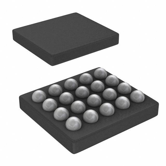
| 描述 | IC LED DVR 3CH MULTIFUNC 20DSBGA |
| 产品分类 | |
| 品牌 | Texas Instruments |
| 数据手册 | |
| 产品图片 |
|
| 产品型号 | TPS68401C4YFFR |
| rohs | 无铅 / 符合限制有害物质指令(RoHS)规范要求 |
| 产品系列 | - |
| 供应商器件封装 | 20-DSBGA |
| 其它名称 | 296-27427-6 |
| 内部驱动器 | 是 |
| 包装 | Digi-Reel® |
| 安装类型 | 表面贴装 |
| 封装/外壳 | 20-UFBGA,DSBGA |
| 工作温度 | -30°C ~ 85°C |
| 恒压 | - |
| 恒流 | 是 |
| 拓扑 | PWM,切换式电容器(充电泵) |
| 标准包装 | 1 |
| 电压-电源 | 2.7 V ~ 5.5 V |
| 电压-输出 | 4.55V |
| 类型-初级 | 背光 |
| 类型-次级 | RGB,白色 LED |
| 输出数 | 3 |
| 频率 | 1.25MHz |


PDF Datasheet 数据手册内容提取
TPS68401, TPS68402 www.ti.com SLVSA68A –MARCH2010–REVISEDJANUARY2011 MULTIFUNCTION 3-CHANNEL LED DRIVERS CheckforSamples:TPS68401,TPS68402 FEATURES • I2CInterface 1 • MultifunctionLEDDriverWithThree • OperatingTemperatureRange:-30ºCto85ºC IndependentChannels APPLICATIONS • IntegratedHighEfficiency1x/1.5xCharge PumpWithAutomaticorManualGainChange • LEDControlforPortableApplications • 3x25.5-mATotalOutputCurrent • AccentLighting(Mood,Personalization,etc.) • 3x25.5-mATotalOutputCurrent • FunctionIndication(Charge,Messages,etc.) • KeypadIllumination/Backlight(WhiteorRGB) • ThreeIndependentProgramExecution Engines(3x16Instructions) • DisplayBacklight • 8-BitPWMWithExponentialControlOption • 8-BitCurrentDACControl • 200-nATypicalShutdownCurrent • AutomaticPower-SaveMode • AutonomousOperationWithoutExternal Control • TriggerI/OforSynchronizingMultipleDevices • OneorTwoGeneralPurposeOutput ControlledViaSerialInterface DESCRIPTION The TPS68401/TPS68402 is an advanced lighting management unit for handheld devices. It has three independent channels optimized for driving RGB LEDs. The built-in fractional charge pump boosts the input voltage to power the LEDs at low input voltage. Channel one can optionally be supplied directly from the battery voltagetoreducepowerconsumptionandimproveefficiency. Attheheartofthedeviceisaprogrammablestatemachinewhichexecutesalightingprogramconsistingofupto 16 instructions per channel. Once the program is loaded through the I2C interface the device is fully independent from the main processor resulting in significant system-level power savings. The device can issue an interrupt to themainprocessorviatheINTpin. The TRIG I/O allows synchronization between multiple devices. A general-purpose output pin is provided which is addressable through the serial interface. In addition, the INT pin can also be configured as general-purpose output. 1 Pleasebeawarethatanimportantnoticeconcerningavailability,standardwarranty,anduseincriticalapplicationsofTexas Instrumentssemiconductorproductsanddisclaimerstheretoappearsattheendofthisdatasheet. PRODUCTIONDATAinformationiscurrentasofpublicationdate. Copyright©2010–2011,TexasInstrumentsIncorporated Products conform to specifications per the terms of the Texas Instruments standard warranty. Production processing does not necessarilyincludetestingofallparameters.
TPS68401, TPS68402 SLVSA68A –MARCH2010–REVISEDJANUARY2011 www.ti.com This integrated circuit can be damaged by ESD. Texas Instruments recommends that all integrated circuits be handled with appropriateprecautions.Failuretoobserveproperhandlingandinstallationprocedurescancausedamage. ESDdamagecanrangefromsubtleperformancedegradationtocompletedevicefailure.Precisionintegratedcircuitsmaybemore susceptibletodamagebecauseverysmallparametricchangescouldcausethedevicenottomeetitspublishedspecifications. FUNCTIONALBLOCKDIAGRAM VOUT VDD R_TO_BATT CPLY1P 8bit DAC CPLY1N 1x/1.5x CPLY2P R Charge Pump 8-bit PWM CPLY2N EN Charge Pump 8bit DAC Control G 8-bit PWM GND Reference TRIM GND 1.25MHz Qpump 8bit DAC Oscillator HF PWM 32768Hz(PWM) B 8-bit PWM CLK32K Ext.PWM clock Control Register PUC Controller/Sequencer SCL Program SDA INT_AS_GPO I2C Register ADDR_SEL0 ADDR_SEL1 ENABLE VDD VDD GPO INT TRIG 2 SubmitDocumentationFeedback Copyright©2010–2011,TexasInstrumentsIncorporated ProductFolderLink(s):TPS68401 TPS68402
TPS68401, TPS68402 www.ti.com SLVSA68A –MARCH2010–REVISEDJANUARY2011 ORDERINGINFORMATION T PACKAGE ORDERABLEPARTNUMBER TOP-SIDEMARKING A YFF TPS68401C4YFFR TPS68401C4YFF -30°Cto85°C RHF TPS68402A0RHFR 24RHF TERMINAL FUNCTIONS NanoFreeYFF PACKAGE PACKAGE MARKING (BOTTOM VIEW) TRIG GND VDD CFLY CFLY 4 1P 2P YMILLL INT C3L2KK GND C1FNLY C2FNLY 3 PA1S YM =YEAR/MONTH DATE CODE EN GPO ADDR ADDR VOUT 2 LLLL=LOTTRACE CODE SEL0 SEL1 S =ASSEMBLYSITE CODE A =MAJOR DIE REVISION 1 =MINOR DIE REVISION SDA SCL R G B 1 P =PREPRODUCTION INDICATOR 0 =PinA1(Filled Solid) E D C B A TERMINAL I/O DESCRIPTION NAME NO. CFLY1P 4B Positiveterminalofchargepumpflycapacitor CFLY1N 3B Negativeterminalofchargepumpflycapacitor CFLY2P 4A Positiveterminalofchargepumpflycapacitor CFLY2N 3A Negativeterminalofchargepumpflycapacitor VDD 4C Powerpin GND 4D Ground VOUT 2A Chargepumpoutput R 1C O Currentsourceoutput,Channel1(Red) G 1B O Currentsourceoutput,Channel2(Green) B 1A O Currentsourceoutput,Channel3(Blue) SCL 1D I I2CSerialinterfaceclockinput SDA 1E I/O I2CSerialinterfacedatainput/output(opendrain) 32.768-kHzclockinput–Ifnoclockpresentonpower-uporafterRESET,usesinternal CLK32K 3D I oscillator EN 2E I Chipenable(activehigh) ADDR_SEL0 2C I I2Caddressselectinput ADDR_SEL1 2B I I2Caddressselectinput INT 3E O Interruptoutput(opendrain,activelow);Canbeconfiguredaspush-pullGPO TRIG 4E I/O Triggerinput/output(opendrain,activelow) GPO 2D O Generalpurposeoutput GND 3C Ground Copyright©2010–2011,TexasInstrumentsIncorporated SubmitDocumentationFeedback 3 ProductFolderLink(s):TPS68401 TPS68402
TPS68401, TPS68402 SLVSA68A –MARCH2010–REVISEDJANUARY2011 www.ti.com RHF PACKAGE - BOTTOMVIEW RHF PACKAGE MARKING -TOPVIEW TERMINAL I/O DESCRIPTION NAME NO. CFLY2P 1 Positiveterminalofchargepumpflycapacitor CFLY1P 2 Positiveterminalofchargepumpflycapacitor VDD 3 Powerpin GND 4 Ground 32.768-kHzclockinput.Ifnoclockpresentonpower-uporafterRESET,usesinternal CLK32K 5 I oscillator. INT 6 O Interruptoutput(opendrain,activelow);Canbeconfiguredaspush-pullGPO. TRIG 7 I/O Triggerinput/output(opendrain,activelow) N/C 8 Notconnected N/C 9 Notconnected N/C 10 Notconnected N/C 11 Notconnected N/C 12 Notconnected SDA 13 I/O I2CSerialinterfacedatainput/output(opendrain) EN 14 I Chipenable(activehigh) SCL 15 I I2CSerialinterfaceclockinput GPO 16 O Generalpurposeoutput. R 17 O Currentsourceoutput,Channel1(Red) G 18 O Currentsourceoutput,Channel2(Green) B 19 O Currentsourceoutput,Channel3(Blue) ADDR_SEL0 20 I I2Caddressselectinput ADDR_SEL1 21 I I2Caddressselectinput VOUT 22 Chargepumpoutput CFLY2N 23 Negativeterminalofchargepumpflycapacitor CFLY1N 24 Negativeterminalofchargepumpflycapacitor 4 SubmitDocumentationFeedback Copyright©2010–2011,TexasInstrumentsIncorporated ProductFolderLink(s):TPS68401 TPS68402
TPS68401, TPS68402 www.ti.com SLVSA68A –MARCH2010–REVISEDJANUARY2011 ABSOLUTE MAXIMUM RATINGS overoperatingfree-airtemperaturerange(unlessotherwisenoted) (1)(2) VALUE UNIT V V (unregulatedinputbatteryvoltage) -0.3to6 V OUT DD INT,GPO,R,G,B,CFLY1N, CFLY1P,CFLY2N,CFLY2P, -0.3toVDD+0.3 Input/Outputvoltagerange(withrespecttoPGND) ADDR_SEL0,ADDR_SEL1 (6.0max) V SDA,SCL,EN,TRIG,CLK32K q Junction-to-ambientthermalresistance 100 °C/W JA P Continuouspowerdissipation Internallylimited W D T Operatingjunctiontemperature -30to125 °C J T Storagetemperature -65to150 °C stg (HBM)Humanbodymodel ±2000 ESDrating V (CDM)Chargeddevicemodel ±100 (1) StressesbeyondthoselistedunderAbsoluteMaximumRatingsmaycausepermanentdamagetothedevice.Thesearestressratings only,andfunctionaloperationofthedeviceattheseoranyotherconditionsbeyondthoseindicatedunderRecommendedOperating Conditionsisnotimplied.Exposuretoabsolutemaximumratedconditionsforextendedperiodsmayaffectdevicereliability. (2) Allvoltagevaluesarewithrespecttonetworkgroundterminal. RECOMMENDED OPERATING CONDITIONS overoperatingfree-airtemperaturerange(unlessotherwisenoted) MIN NOM MAX UNIT V Unregulatedinputbatteryvoltage 2.7 3.6 5.5 V DD INT,GPO, ADDR_SEL0, 0 5.5 V ADDR_SEL1 SDA,SCL,EN, 0 1.8 V TRIG CLK_32K Externalclockfrequency 16 32 64 kHz T Operatingambienttemperature -30 85 °C A Flyingcapacitor 0.47 mF Inputcapacitor(V ) 1 mF DD Outputcapacitor(V ) 1 mF OUT SCA,SDApull-upresistorvalue 10 kΩ INTpull-upresistorvalue 10 kΩ Copyright©2010–2011,TexasInstrumentsIncorporated SubmitDocumentationFeedback 5 ProductFolderLink(s):TPS68401 TPS68402
TPS68401, TPS68402 SLVSA68A –MARCH2010–REVISEDJANUARY2011 www.ti.com ELECTRICAL CHARACTERISTICS V =3.6V±5%,T =25ºC(unlessotherwisenoted) BAT A PARAMETER TESTCONDITIONS MIN TYP MAX UNIT SUPPLYCURRENT Shutdowncurrent EN=0 0.2 2.0 mA EN=1;CHIP_EN=0 1 2.0 Ext.32-kHzclocknotrunning Standbycurrent mA EN=1;CHIP_EN=0 1 2.0 Ext.32-kHzclockrunning EN=1,CHIP_EN=1 Ext.32-kHzclockrunning C/P,G&Bchanneldisabled R_TO_BATT=1(Rchannelenabled) 180 [CLK_DET_EN:INT_CLK_EN]=00b (clockdetectiondisabled) I =5mA,50%dutycycle LED EN=1,CHIP_EN=1 C/PandLEDdriversdisabled [CLK_DET_EN:INT_CLK_EN]=10b 190 (automaticclocksourceselection) PWRSAVE_EN=0 EN=1,CHIP_EN=1 IDD Normalmodesupplycurrent C/Pin1xmode,noload(1), 70 mA LEDdriversdisabled Ext.32-kHzclockrunning EN=1,CHIP_EN=1 C/Pin1.5xmode,noload(1), 1700 LEDdriversdisabled EN=1,CHIP_EN=1 C/Pin1xmode,noload(1), 650 LEDdriversenabled Ext.32-kHzclockrunning EN=1,CHIP_EN=1 C/Pin1xmode,5-mAloadLEDdrivers 800 enabled Ext.32-kHzclockrunning EN=1,CHIP_EN=1 10 CLK32Kactive Powersavecurrent mA EN=1,CHIP_EN=1 190 Internaloscillatorrunning STARTUP t Startuptime STANDBYtoNORMALmode 500 1000 ms STARTUP BOOSTVOLTAGE(V ) OUT 1xmode,noload(1) V DD V Outputvoltage V OUT 1.5xmode,V =3.6V,noload(1) 4.55 DD V Automaticgainchangehysteresis C/Pinautomaticmode,noload(1) 200 mV HYS Continuousoutputcurrent 150 I V <1V 150 mA OUT OUT Maxoutputcurrent V >1V 150 250 OUT f Switchingfrequency 1.25 MHz S 1xmode(V -V )/I 1.1 DD OUT OUT Z Openloopoutputimpedance Ω O 1.5xmode(2) 4.1 Turnontimefrom1xto1.5xmode. V =3.6V 50 DD t ms ON Turnontimefromoffto1.5xmode. V =0V 100 OUT (1) No-loadmeasurementconditionisasfollows:DACsetting=default(17.5mA);PWM=0;Outputconnectedtogroundvia150-Ω resistor. (2) ChargepumpImpedanceismeasuredatV =3V,I =50mAfollows:[V (I =0)–V (I )]/I DD OUT OUT OUT OUT OUT OUT 6 SubmitDocumentationFeedback Copyright©2010–2011,TexasInstrumentsIncorporated ProductFolderLink(s):TPS68401 TPS68402
TPS68401, TPS68402 www.ti.com SLVSA68A –MARCH2010–REVISEDJANUARY2011 ELECTRICAL CHARACTERISTICS (continued) V =3.6V±5%,T =25ºC(unlessotherwisenoted) BAT A PARAMETER TESTCONDITIONS MIN TYP MAX UNIT INTERNALOSCILLATOR T =25ºC -4 4 A f Internaloscillatorfrequency % OSC -30ºC≤T ≤85ºC -7 7 A OUTPUTCHANNELS(R,G,B) V LEDforwardvoltage 1.5 LED V Driversaturationvoltage I =17.5mA(3) 50 100 mV DRP R,G,B LEDcurrent Perchannel 0 25.5 mA LEDcurrentresolution 8 Bit I R,G,B LEDcurrentaccuracy I =17.5mA -4 4 % R,G,B LEDcurrentmatching I =17.5mA,V =3.0V 1 2 % R,G,B f PWM_HF=1 558 Internalhighfrequencyoscillator f PWMfrequency Hz PWM PWM_HF=0 256 InternalclockorCLK_32K T =25ºC 0.1 A I Pinleakagecurrent mA LEAK -30ºC≤T ≤85ºC 1 A PWM PWMresolution 8 Bit RES LOGICINPUTLEVELS(EN) V Inputlowlevel 0.5 V IL V Inputhighlevel 1.2 V IH I ,I Inputbiascurrent V =0Vto1.65V -1 1 mA IH IL EN t Inputdelay ENpinlowtohigh 2 ms delay LOGICINPUTLEVELS(SCL,SDA,TRIG,CLK_32K) V Inputlowlevel V =1.65Vto3.6V 0.2xV V IL EN EN V Inputhighlevel V =1.65Vto3.6V 0.8xV V IH EN EN I ,I Inputbiascurrent -1.0 1.0 mA IH IL f I2Cclockfrequency 400 kHz SCL LOGICINPUTLEVELS(ADD_SEL0,ADD_SEL1) V Inputlowlevel 0.2xV V IL DD V Inputhighlevel 0.8xV V IH DD I ,I Inputbiascurrent VADD_SEL0,ADD_SEL1=3.6V -1.0 1.0 mA IH IL LOGICOUTPUTLEVELS(SDA,TRIG,INTpinasINT) V Outputlowlevel I =3mAthroughpull-up 0.3 0.5 V OL OUT INTpinasINT(opendrain),INT=high, I Outputleakagecurrent 1.0 mA IL V =0Vto1.65V INT LOGICOUTPUTLEVELS(GPO,INTpinasGPO) V Outputlowlevel I =3mA 0.3 0.5 V OL OUT V Outputhighlevel I =-2mA V -0.5 V -0.3 V OH OUT DD DD (3) I atV =0.9xI at(V -V )=1V OUT DRP OUT DD LED Copyright©2010–2011,TexasInstrumentsIncorporated SubmitDocumentationFeedback 7 ProductFolderLink(s):TPS68401 TPS68402
TPS68401, TPS68402 SLVSA68A –MARCH2010–REVISEDJANUARY2011 www.ti.com DESCRIPTION OF CHARGE PUMP OPERATION The TPS68401/TPS68402 includes a regulated fractional charge pump with bypass mode. It is used to boost the supply voltage for the output drivers when the battery voltage is close to or below the forward bias voltage of the LEDs. In 1.5x mode V is boosted to 1.5x V or 4.55 V, whichever value is lower. In 1x (bypass) mode the OUT DD outputisconnecteddirectlytotheinputsupply. The charge pump is controlled with two CP_MODE bits in the CONFIG register. When disabled, V is OUT connected to ground through a 300-kΩ resistive path. The user can manually select 1x and 1.5x mode or select automatic mode. When automatic mode is enabled, the charge pump will operate in bypass mode as long as the inputsupplyvoltageissufficienttodrivetheLEDs.Dropoutvoltageofallthreechannelsismonitoredandcharge pump gain is set to 1.5x if any one driver does not have enough headroom to drive the LED. When the part enters Power Save mode the output capacitor is connected to the input supply through a resistive path. See PowerSavemodedescriptionfordetails. The mode selection logic utilizes digital filtering to prevent glitches of the supply voltage from triggering gain changes. If R-driver current source is connected to battery (CONFIG register, bit R_TO_BATT set to 1) voltage monitoringisdisabledinRoutput,butstillfunctionalinGandBoutput. BYPASS VDD CIN WEAK 1x CP_MODE[1:0] 1x/1.5x REG VOUT C/P COUT CP_MODE[1:0] =OFF Figure1. FunctionalModelofChargePump 8 SubmitDocumentationFeedback Copyright©2010–2011,TexasInstrumentsIncorporated ProductFolderLink(s):TPS68401 TPS68402
TPS68401, TPS68402 www.ti.com SLVSA68A –MARCH2010–REVISEDJANUARY2011 5.5 4.5 V] E E [UT MOD M O D VO x 1x 5 1. 3.0 5.5 V [V] DD Figure2. ChargePumpOutputVoltage LED DRIVER OPERATIONAL DESCRIPTION The TPS68401/TPS68402 has three independent constant current LED drivers with 8-bit PWM control. Output current is programmed through the I2C register and ranges from 0 mA to 25.5 mA with 8-bit resolution. PWM duty cycle is controlled either by program instructions or R/G/B PWM registers. Green and blue channels are always connected to the charge pump output V . The red channel is connected to either V or V OUT OUT DD depending on R_TO_BAT bit setting of the CONFIG register. If red channel is connected to V , automatic DD chargepumpgaincontrolisnotusedforthisoutput.ConnectingtheredchanneltoV providesbetterefficiency DD whendrivingLEDswithlowVForthesupplyvoltageishighenoughtodriveaLEDwithhighVF. PWM frequency is either 256 Hz or 558 Hz and is selected through PWM_HF bit in the CONFIG register. Linear andlogarithmicPWMduty-cycle-to-inputresponseisselectablethroughtheLOG_ENbitoftheENABLEregister. LOG_EN bit controls PWM response for all three channels. Logarithmic response is approximated by piece-wise-linearfunctionasshownbelow. When the external clock source is selected for driving the PWM, PWM frequency scales with the external clock frequency.Nominal256-HzPWMfrequencyrequiresexternalclockfrequencyof32.768kHz. Copyright©2010–2011,TexasInstrumentsIncorporated SubmitDocumentationFeedback 9 ProductFolderLink(s):TPS68401 TPS68402
TPS68401, TPS68402 SLVSA68A –MARCH2010–REVISEDJANUARY2011 www.ti.com PWMCONTROL Table1.PWMValueandOutputinLINandEXPMode PWMOUTPUT PWMOUTPUT PWMREGISTERVALUE PWMREGISTERVALUE LIN EXP LIN EXP 0 0 0 128 128 64 1 1 0 129 129 65 2 2 1 130 130 66 3 3 1 131 131 67 4 4 2 132 132 68 5 5 2 133 133 69 ... ... ... ... ... ... 61 61 30 189 189 125 62 62 31 190 190 126 63 63 31 191 191 127 64 64 32 192 192 129 65 65 32 193 193 131 66 66 33 194 194 133 ... ... ... ... ... ... 125 125 62 253 253 251 126 126 63 254 254 253 127 127 63 255 255 255 256 224 EXP LIN 192 S] K C 160 TI [ T U TP 128 U O M W 96 P 64 32 0 0 32 64 96 128 160 192 224 256 PWM LINEAR INPUT Figure3. GraphofPWMOutputvs.PWMInput 10 SubmitDocumentationFeedback Copyright©2010–2011,TexasInstrumentsIncorporated ProductFolderLink(s):TPS68401 TPS68402
TPS68401, TPS68402 www.ti.com SLVSA68A –MARCH2010–REVISEDJANUARY2011 Table2.LEDChannelOutputCurrentControl REGISTER BITS VALUE CHANNELCURRENT 0x00 0.0mA 0x01 0.1mA ↕ ↕ 0xAE 17.4mA R_CURRENT, G_CURRENT, 7:0 0xAF 17.5mA B_CURRENT 0xB0 17.6mA ↕ ↕ 0xFE 25.4mA 0xFF 25.5mA DATA TRANSMISSION TPS68401/TPS68402 features an I2C slave interface for communication to a controlling microprocessor. SDA, SCL, CLK_32K and TRIG pins input levels are defined by EN pin. EN pin is used as voltage reference for logic inputsandthereforenodedicatedVIOpinisrequired. VDD EN BInupffuetr SDA Level Shifter SCL Level Shifter CLK32K SLheifvteelr TRIG SLheifvteelr Figure4. InternalLogicLevelShifters Copyright©2010–2011,TexasInstrumentsIncorporated SubmitDocumentationFeedback 11 ProductFolderLink(s):TPS68401 TPS68402
TPS68401, TPS68402 SLVSA68A –MARCH2010–REVISEDJANUARY2011 www.ti.com SUBADDRESS DEFINITION SlaveAddress+R/nW SubAddress Data Start G3 G2 G1 G0 A2 A1 A0 R/nW ACK S7 S6 S5 S4 S3 S2 S1 S0 ACK D7 D6 D5 D4 D3 D2 D1 D0 ACK Stop Figure5. SubaddressinI2CTransmission Start –StartCondition ACK –Acknowledge G(3:0) –GroupID:Addressfixedat0110b S(7:0) –Subaddress:definedperregistermap –Deviceaddress:Deviceaddressisselectablevia A(2:0) D(7:0) –Data;Datatobeloadedintothedevice ADDR_SELinputpin. R/nW –Read/notWriteselectbit Stop –Stopcondition Table3. SubaddressBits DefinedbyADDR_SELInputs ADDR_SEL A[2:0] [1:0] 00 010 01 011 10 100 11 101 The address bits used in the slave address portion of the I2C transaction are defined by the device pins ADDR_SEL1 and ADDR_SEL0 (combined as ADDR_SEL [1:0] above). The table above gives the values of the addressbitsforallcombinationsofADDR_SEL1andADDR_SEL0. I2C BUS OPERATION TheI2Cbusisacommunicationslinkbetweenacontrollerandaseriesofslaveterminals.Thelinkisestablished using a two-wired bus consisting of a serial clock signal (SCL) and a serial data signal (SDA). The serial clock is sourced from the controller in all cases where the serial data line is bi-directional for data communication between the controller and the slave terminals. Each device has an open drain output to transmit data on the serial data line. An external pull-up resistor must be placed on the serial data line to pull the drain output high duringdatatransmission. Data transmission is initiated with a start bit from the controller as shown in Figure 6. The start condition is recognized when the SDA line transitions from high to low during the high portion of the SCL signal. Upon reception of a start bit, the device will receive serial data on the SDA input and check for valid address and control information. If the appropriate group and address bits are set for the device, then the device will issue an acknowledge pulse and prepare the receive subaddress data. Subaddress data is decoded and responded to as per the Register Map section of this document. Data transmission is completed by either the reception of a stop condition or the reception of the data word sent to the device. A stop condition is recognized as a low to high transition of the SDA input during the high portion of the SCL signal. All other transitions of the SDA line must occur during the low portion of the SCL signal. An acknowledge is issued after the reception of valid address, sub-address and data words. The I2C interface will auto-sequence through register addresses, so that multiple datawordscanbesentforagivenI2Ctransmission. 12 SubmitDocumentationFeedback Copyright©2010–2011,TexasInstrumentsIncorporated ProductFolderLink(s):TPS68401 TPS68402
TPS68401, TPS68402 www.ti.com SLVSA68A –MARCH2010–REVISEDJANUARY2011 . . . SDA . . . SCL 1 2 3 4 5 6 7 8 9 START CONDITION ACKNOWLEDGE STOPCONDITION Figure6. I2CStart/Stop/AcknowledgeProtocol tLOW tr( tF tH(STA) SCL tH(STA) tH(DAT) tHIGH tS(DAT) tS(STA) tS(STO) SDA t(BUF) P S S P Figure7. I2CDataTransmissionTiming Copyright©2010–2011,TexasInstrumentsIncorporated SubmitDocumentationFeedback 13 ProductFolderLink(s):TPS68401 TPS68402
TPS68401, TPS68402 SLVSA68A –MARCH2010–REVISEDJANUARY2011 www.ti.com DATA TRANSMISSION TIMING V =3.6±5%,T =25ºC,C =100pF(unlessotherwisenoted) BAT A L PARAMETER TESTCONDITIONS MIN TYP MAX UNIT 100 f Serialclockfrequency KHz (SCL) 400 Busfreetimebetweenstopandstart SCL=100kHz 4.7 t µs (BUF) condition SCL=400kHz 1.3 SCL=100kHz 50 t Tolerablespikewidthonbus ns (SP) SCL=400kHz SCL=100kHz 4.7 t SCLlowtime µs LOW SCL=400kHz 1.3 SCL=100kHz 4 t SCLhightime µs HIGH SCL=400kHz 0.6 SCL=100kHz 250 t SDA→SCLsetuptime ns S(DAT) SCL=400kHz 100 SCL=100kHz 4.7 t Startconditionsetuptime µs S(STA) SCL=400kHz 0.6 SCL=100kHz 4 t Stopconditionsetuptime µs S(STO) SCL=400kHz 0.6 SCL=100kHz 0 3.45 t SDA→SCLholdtime µs H(DAT) SCL=400kHz 0 0.9 SCL=100kHz 4 t Startconditionholdtime µs H(STA) SCL=400kHz 0.6 SCL=100kHz 1000 t RisetimeofSCLSignal ns r(SCL) SCL=400kHz 300 SCL=100kHz 300 t FalltimeofSCLSignal ns f(SCL) SCL=400kHz 300 SCL=100kHz 1000 t RisetimeofSDASignal ns r(SDA) SCL=400kHz 300 SCL=100KHz 300 t FalltimeofSDASignal ns f(SDA) SCL=400kHz 300 FUNCTIONAL DESCRIPTION OF DEVICE PINS ADDR_SEL0 AND ADDR_SEL1 PINS ADDR_SEL0 and ADDR_SEL1 pins define the chip I2C address. Pins are referenced to V signal level. See DD DataTransmissionsectionforI2Caddressdefinitions. GENERAL PURPOSE OUTPUT PIN The TPS68401/TPS68402 has one dedicated general purpose output pin (GPO) with digital CMOS output. High-level output voltage is defined by V and no pull-up resistor is needed. GPO output is controlled by GPO DD bitoftheGPOregister. INT PIN The INT pin is used to issue an interrupt to a host processor when END instruction is executed and the INT bit is set (see Instruction Description section for details). The INT pin can also be configured as a GPO pin by setting the INT_AS_GPO bit of the GPO register. When configured as INT pin it has an open drain output and requires anexternalpull-upresistor.AsGPOpinithasadigitalCMOSoutput,high-leveloutputvoltageisdefinedbyV , DD andnopull-upresistorisneeded.InGPOmodetheoutputiscontrolledbytheINTbitoftheGPOregister. 14 SubmitDocumentationFeedback Copyright©2010–2011,TexasInstrumentsIncorporated ProductFolderLink(s):TPS68401 TPS68402
TPS68401, TPS68402 www.ti.com SLVSA68A –MARCH2010–REVISEDJANUARY2011 TRIG PIN TRIG pin is used to send and receive trigger pulses between multiple TPS68401/TPS68402 devices for pattern synchronization. TRIG is an open drain output and requires an external pull-up resistor. External trigger input signalmustbeatleasttwo32-kHzclockcycleslongtoberecognized.Triggeroutputsignalisthree32-kHzclock cycleslong.IfTRIGpinisnotusedonapplication,itshouldbeconnectedtoGND. CLK_32K PIN CLK_32K pin is used for connecting external 32.768-kHz clock to TPS68401/TPS68402. Connecting several devices to the same clock source ensures synchronous instruction execution. When external clock source is used the internal oscillator is shut down during automatic power save mode to achieve lowest possible current consumption. An external clock source is not required for device operation. If external clock is not used, CLK_32KpinshouldbeconnectedtoGND. CLK_32K EXTERNAL CLOCK DETECTION The instruction execution engine and PWM are clocked either by an internal 32.768-kHz or an external clock. The user can manually select internal or external clock or enable automatic clock source selection. In automatic mode the TPS68401/TPS68402 monitors the CLK32K pin; If external clock frequency is < 15 kHz, stuck-at-zero, or stuck-at-one, the clock detector indicates that no external clock is present and switches to internal clock source. It switches back to external clock source once the external clock is detected again. In any mode (manual or automatic selection) the clock source can be checked by reading the EXT_CLK_USED bit of the STATUS register. Clock source selection is controlled by CONFIG register bits INT_CLK_EN and CLK_DET_EN. External clockdetectionisdisabledinPOWERSAVEmode. When external clock source is selected, instruction timing and PWM frequency scale with the external clock frequency.Nominalexternalclockfrequencyis32.768kHz. MODES OF OPERATION RESET In the RESET mode all the internal registers are reset to the default values. Reset is initiated if 0xFFh is written into the RESET register or internal power-up clear (PUC) is activated. PUC will activate when supply voltage is connected to V pin or when the supply voltage drops below the nPUC_VIL level. Once V rises above DD DD nPUC_VIH, PUC is released and the chip will continue to the STANDBY mode. CHIP_EN control bit is low after PUCbydefault. SHUTDOWN WhenevertheENpinispulledlowthedeviceentersSHUTDOWNmode.Allfunctionsaredisabled,includingthe serialinterface.Thisisthelowestpowermode. STANDBY STANDBY mode is entered if the CHIP_EN bit of the ENABLE register is set to 0 and reset is not active. Registers can be written to in this mode with the exception of the EXEC bits of the ENABLE register (R_EXEC[1:0],G_EXEC[1:0],B_EXEC[1:0]).Controlbitsareeffectiveafterstartup. STARTUP When CHIP_EN bit of the ENABLE register is written 1 and EN pin is high, the chip executes the internal startup sequence to power up analog blocks (V , bias, oscillator etc.). If the chip temperature rises too high, the over REF temperature shutdown (OTS) disables the chip and automatically re-enters STARTUP mode, until no thermal shutdowneventispresent. NORMAL During NORMAL mode the user controls the chip using the control registers. If EN pin is set low, the CHIP_EN bitisresetto0. Copyright©2010–2011,TexasInstrumentsIncorporated SubmitDocumentationFeedback 15 ProductFolderLink(s):TPS68401 TPS68402
TPS68401, TPS68402 SLVSA68A –MARCH2010–REVISEDJANUARY2011 www.ti.com POWER SAVE In POWER SAVE mode analog blocks are disabled to minimize power consumption. See the Power Save Mode sectionforfurtherinformation. MODE TRANSITIONS Setting the CHIP_EN bit of the ENABLE register to 0 resets the program counters (PC) but does not change the LED controller operational mode (see NORMAL MODE settings). Pulling the EN pin low resets the CHIP_EN bit andPCbutdoesnotaffectoperationalmode(seeNORMALMODEsettings). POWER OFF nPUC=0 RESET=0xFFh or nPUC=0 RESET nPUC=1and EN pin=Low nPUC=1and EN pin=Low SHUTDOWN EN pin=High EN pin=High STANDBY CHIP_EN bit=0 CHIP_EN bit=1 STARTUP TSD=1 TSD=1 TSD=0 TSD RECOVERY TSD=0 TSD=1 NORMAL Disable Enable Power Save Power Save POWER SAVE Figure8. DeviceStartupFlowandModesofOperation 16 SubmitDocumentationFeedback Copyright©2010–2011,TexasInstrumentsIncorporated ProductFolderLink(s):TPS68401 TPS68402
TPS68401, TPS68402 www.ti.com SLVSA68A –MARCH2010–REVISEDJANUARY2011 POWER SAVE MODE Automatic power save mode is enabled when PWRSAVE_EN bit in the CONFIG register is set to 1. In power save mode all analog blocks are powered down with exception of charge pump protection circuits, provided external clock source is used to run the PWM. If internal clock source has been selected, only charge pump and LED drivers are disabled and the digital part of the LED controller remains active. In both cases charge pump enters a special 1x mode to keep the output at battery level. During program execution the device can enter power save if there is no PWM activity in R, G and B outputs for > 50ms. To prevent the device from entering power-save mode for short periods of time the device does a command look-ahead. In every instruction cycle R, G, B commands are analyzed, and if there is sufficient time left with no PWM activity, device will enter power save mode. In power save mode program execution continues uninterruptedly. When a command that requires PWM activity is executed, the device starts up automatically. The following table describes commands and conditions that can activate power save mode. All channels (R, G, and B) need to meet power save condition in ordertoenablepowersave. POWER SAVE MODE can only be entered when no channel is in the LOAD MODE, all PWM values are zero or channelisdisabled,andC/PmodeiseitherOFForAutomatic. Table4.RequirementsforPowerSaveByCommand COMMAND POWERSAVEREQUIREMENT WAIT EnterpowersaveonlyifPWMiszeroandwaitisgreaterthen50ms. RAMP EnterpowersaveonlyiframpendswithPWMsettozeroandthereis50msbeforethenextcommand. TRIGGER EnterpowersaveonlyifPWMiszerowhilewaitingfortrigger. END EnterpowersaveonlyifPWMiszeroorresetbitofcommandissetto1. SET EnterpowersaveonlyifPWMissettozeroandthenextcommandgeneratesatleasta50-mswait. Other Cannotenterpowersavemode LED CONTROLLER OPERATIONAL MODES (NORMAL MODE) In NORMAL MODE, operation of the red, green, and blue LED controller is defined independently by the OP_MODE, and respective R/G/B_PC, R/G/B_PWM, and R/G/B_CURRENT registers. The R/G/B CURRENT registers define the maximum output current for the respective channel. MODE control bits are synchronized to a 32-kHzclock. In the following, PC denotes either R_PC, G_PC, or B_PC program counter. MODE denotes either R_MODE, G_MODE,orB_MODEbitsoftheOP_MODEregister. DISABLEDMODE LEDoutputcurrentissetto0andPCcounterisreset. LOADMODE The device can store 16 16-bit commands for each channel (R, G, B). Due to the 8-bit format of the I2C protocol two writes are required to load a single instruction. The device supports auto-increment addressing to reduce program load time. Register address is incremented after each 8 data bits which allows the whole program memory to be written in a single I2C write sequence. Program memory is defined in the register table. Read / write access to program memory is allowed only in LOAD mode and only to the channel in LOAD mode. LOAD mode resets respective channel’s PC. Program execution on all other channels is halted and PWM value remains static while at least one channel is in LOAD mode. Program execution continues when all channels are outofLOADprogrammode. RUNMODE In RUN mode the LED controller executes instructions stored in program memory. Execution is controlled by the R, G, and B program counters (R_PC, G_PC, B_PC) and the ENABLE register. For details refer to RUN MODE OPTIONS section. Program start position can be determined by writing to the PC registers. If program counter runs to end (15) the next command will be executed from program location 0. If internal PWM clock source is selected in RUN mode, the LED controller must be disabled (MODE = 00b) before disabling the chip (with CHIP_EN bit or EN pin) to ensure that the sequence starts from the correct program counter (PC) value when restartingthesequence.PCregistersaresynchronizedtoa32-kHzclock. Copyright©2010–2011,TexasInstrumentsIncorporated SubmitDocumentationFeedback 17 ProductFolderLink(s):TPS68401 TPS68402
TPS68401, TPS68402 SLVSA68A –MARCH2010–REVISEDJANUARY2011 www.ti.com DIRECTMODE In DIRECT mode the LED channels can be controlled independently through the I2C interface. For each channel there is a PWM control register (R_PWM, G_PWM, B_PWM) which contains the PWM duty cycle. If the charge pump is set to automatic 1x / 1.5x mode selection, PWM values need to be written 0 before disabling the drivers (MODE=00b)toensureproperautomaticgainchangeoperation. MODETRANSITIONS Atransitionbetweenoperationalmodesabortstheinstructionbeingexecuted(ifany),resetsthePCandsetsthe PWMdutycycleto0.Thechannelcurrentsettingisnotaffected. 10b RUN 10b 10b 10b 00b 11b 01b DISABLED 11b 01b 00b 00b 00b DIRECT LOAD 11b 01b 01b 11b NORMALMODE Bit settings refer to the R/G/B_MODE[1:0] bits of the OP_MODE register. Figure9. OperationalModesofLEDControllerinNORMALModeofOperation RUN MODE SETTINGS Run mode is set independently for each channel in the ENABLE register. In the following PC denotes either R_PC, G_PC, or B_PC program counter. EXEC denotes either R_EXEC, G_EXEC, or B_EXEC bits of the ENABLEregister. HOLD Wait until current command is finished then stop while EXEC[1:0] = 00b (Hold). PC can be read or written only in thismode. STEP ExecuteinstructiondefinedbyPC,incrementPCandchangeEXEC[1:0]to00b(Hold). 18 SubmitDocumentationFeedback Copyright©2010–2011,TexasInstrumentsIncorporated ProductFolderLink(s):TPS68401 TPS68402
TPS68401, TPS68402 www.ti.com SLVSA68A –MARCH2010–REVISEDJANUARY2011 CONTINUE StartprogramexecutionatPCvalue,incrementPCandcontinue. EXECUTE ExecuteinstructiondefinedbyPC,donotupdatePC,changeEXEC[1:0]to00b(Hold). MODETRANSITIONS A transition between run modes does not abort the instruction being executed. PC is updated before mode transition.NotethatPCisalsoincrementedwhentransitioningoutofEXECUTEmode. 10b CONTINUE 10b 10b 10b 00b 11b 01b HOLD 11b 01b 11b or 00b 01b or 00b EXECUTE 00b STEP 01b 11b RUN MODE Bit settings refer to the R/G/B_EXEC[1:0] bits of the ENABLE register. Figure10. RunModeStateDiagram INSTRUCTION DESCRIPTION The three channels are independent, except for the trigger connections between the channels. The following tabledescribesthebinaryformatused.Inthisimplementation,thereare16programstepsavailableperchannel. Copyright©2010–2011,TexasInstrumentsIncorporated SubmitDocumentationFeedback 19 ProductFolderLink(s):TPS68401 TPS68402
TPS68401, TPS68402 SLVSA68A –MARCH2010–REVISEDJANUARY2011 www.ti.com ct e el S ct ce ele et ut Ext.clock(CLK32K) ClockSour 0G1 PWM_HF PrePrescaleSscale Clockforsteptimecounter StepSteptimesTime IncrInc/Decement Currentvalueoftriggerpoint PWMOutp RunningCounterValue Free Div16or Comparator Running Int.32kHz clock 1 512 Counter Counter Counter x2 G1 0 HF PWM clock 1 Figure11. SimplifiedBlockDiagramofPWM RAMP / WAIT B15 B14 B13 B12 B11 B10 B9 B8 B7 B6 B5 B4 B3 B2 B1 B0 0 x x x x x x x x x x x x x x x prescale sign steptime numberofsteps 0=16 0=INC 1to63 0to127 1=512 1=DEC The ramp command generates a PWM ramp starting from the current value. At each ramp step the PWM value is incremented or decremented by one. Time for one step is defined by prescale and step time bits. The number of increments executed by the instruction is defined by number of steps which has a maximum value of 127 or half of full scale. If, during a ramp command, PWM reaches minimum / maximum (0 / 255), the ramp command will continue for the remaining number of steps without changing the PWM value (PWM value saturates). This enablestherampcommandtobeusedascombinedrampandwaitcommandinsingleinstruction. Rampcommandcanbeusedasasinglesteptimewaitinstructionwhenincrementiszero. SET PWM B15 B14 B13 B12 B11 B10 B9 B8 B7 B6 B5 B4 B3 B2 B1 B0 0 1 0 0 0 0 0 0 x x x x x x x x PWMvalue SetPWMoutputvaluefrom0to255inasingleinstruction. 20 SubmitDocumentationFeedback Copyright©2010–2011,TexasInstrumentsIncorporated ProductFolderLink(s):TPS68401 TPS68402
TPS68401, TPS68402 www.ti.com SLVSA68A –MARCH2010–REVISEDJANUARY2011 BRANCH B15 B14 B13 B12 B11 B10 B9 B8 B7 B6 B5 B4 B3 B2 B1 B0 1 0 1 x x x x x x x x x x x x x loopcount notused stepnumber 0to63(0=loopforever) Loop instruction. Code between (step number) and BRANCH command will be executed (loop count + 1) times. Set(loopcount)=0forinfinitelooping.Nestedloopingissupported.Thenumberofnestedloopsisnotlimited. GO TO START B15 B14 B13 B12 B11 B10 B9 B8 B7 B6 B5 B4 B3 B2 B1 B0 0 0 0 0 0 0 0 0 0 0 0 0 0 0 0 0 Commandresetsprogramcounterregisterandcontinuesexecutingprogramfromthe00Hlocation. END B15 B14 B13 B12 B11 B10 B9 B8 B7 B6 B5 B4 B3 B2 B1 B0 1 1 0 INT RST x x x x x x x x x x x interupt reset 0=KeepthecurrentPWMvalue 1=SetPWMvalueto0 0=Donotissueinterrupt 1=Issueinterruptandsetcorrespondingstatusbithigh.Interruptisclearedbyreadinginterruptstatusregister. Stopsprogramexecution.Set(interrupt)=1toissueaninterruptontheINTpin.IfINTisuseditmustbecleared beforepullingtheENpinloworwritingCHIP_ENlow. TRIGGER B15 B14 B13 B12 B11 B10 B9 B8 B7 B6 B5 B4 B3 B2 B1 B0 1 1 1 EXT x x B G R EXT x x B G R x Waitfortrigger Issuetrigger R=RED;G=GREEN;B=BLUE;EXT=EXTERNAL R=RED;G=GREEN;B=BLUE;EXT=EXTERNAL 1=Waitfortriggerfromspecifiedchannel. 1=Issuetriggerforspecifiedchannel. Ownchannelpositionisignored. Ownchannelpositionisignored. 0=Continuewithoutwait 0=Continuewithoutissuingtrigger Used to synchronize channels and / or multiple units. The wait for trigger command is executed until all defined trigger have been received. An external trigger is ignored by the issuing channel / device. External trigger input signalmustbeatleasttwo32-kHzclockcycleslongtoberecognized.Triggeroutputsignalisthree32-kHzclock cycles long. External trigger signal is active low, i.e. when trigger is send / received the pin is pulled to GND. Sent external trigger is masked, i.e. the device which has sent the trigger will not recognize it. If send and wait externaltriggerareusedonthesamecommand,thesendexternaltriggerisexecutedfirst,thenthewaitexternal trigger.Channel(R,G,orB)waitingforitsowntriggerisnotallowed. Copyright©2010–2011,TexasInstrumentsIncorporated SubmitDocumentationFeedback 21 ProductFolderLink(s):TPS68401 TPS68402
TPS68401, TPS68402 SLVSA68A –MARCH2010–REVISEDJANUARY2011 www.ti.com Table5.ADDRESSREGISTERMAP ADDRESS DEFAULT REGISTER NAME DESCRIPTION (HEX) VALUE 0 0 ENABLE 00000000 Chipenableandexecutioncontrol 1 1 OP_MODE 00000000 RGBoperatingmodecontrol 2 2 R_PWM 00000000 RedchannelPWMvalue 3 3 G_PWM 00000000 GreenchannelPWMvalue 4 4 B_PWM 00000000 BluechannelPWMvalue 5 5 R_CURRENT 10101111 Redchannelcurrentlimitvalue 6 6 G_CURRENT 10101111 Greenchannelcurrentlimitvalue 7 7 B_CURRENT 10101111 Bluechannelcurrentlimitvalue 8 8 CONFIG 00000000 Chargepumpconfiguration 9 9 R_PC 00000000 Redchannelprogramcountervalue 10 0A G_PC 00000000 Greenchannelprogramcountervalue 11 0B B_PC 00000000 Bluechannelprogramcountervalue 12 0C STATUS 00000000 Clockandinterruptstatus 13 0D RESET 00000000 Devicereset 14 0E GPO 10000000 GPOconfigurationandvalue 15 N/A N/A N/A Registernotimplemented 16 10 PROG_MEM_R1_H 00000000 Redchannelinstruction1MSB 17 11 PROG_MEM_R1_L 00000000 Redchannelinstruction1LSB ... ... ... ... ... 46 2E PROG_MEM_R16_H 00000000 Redchannelinstruction16MSB 47 2F PROG_MEM_R16_L 00000000 Redchannelinstruction16LSB 48 30 PROG_MEM_G1_H 00000000 Greenchannelinstruction1MSB 49 31 PROG_MEM_G1_L 00000000 Greenchannelinstruction1LSB ... ... ... ... ... 78 4E PROG_MEM_G16_H 00000000 Greenchannelinstruction16MSB 79 4F PROG_MEM_G16_L 00000000 Greenchannelinstruction16LSB 80 50 PROG_MEM_B1_H 00000000 Bluechannelinstruction1MSB 81 51 PROG_MEM_B1_L 00000000 Bluechannelinstruction1LSB ... ... ... ... ... 110 6E PROG_MEM_B16_H 00000000 Bluechannelinstruction16MSB 111 6F PROG_MEM_B16_L 00000000 Bluechannelinstruction16LSB 22 SubmitDocumentationFeedback Copyright©2010–2011,TexasInstrumentsIncorporated ProductFolderLink(s):TPS68401 TPS68402
TPS68401, TPS68402 www.ti.com SLVSA68A –MARCH2010–REVISEDJANUARY2011 ENABLE REGISTER (ENABLE) Address–0x00h DATABIT D7 D6 D5 D4 D3 D2 D1 D0 FIELDNAME LOG_EN CHIP_EN R_EXEC[1:0] G_EXEC[1:0] B_EXEC[1:0] READ/WRITE R/W R/W R/W R/W R/W R/W R/W R/W RESETVALUE 0 0 0 0 0 0 0 0 FIELDNAME BITDEFINITION LOG_EN Enablelogarithmiccurrentadjustmentmode CHIP_EN Chipenable:ForcingENpinlowresetsCHIP_ENtozero.Seestatediagramfordetails. Programexecutioncontrolforredchannel 00b–Hold:Finishcurrentinstruction,thenstopuntilR_EXEC[1:0]changes. R_EXEC[1:0] 01b–Step:Finishcurrentinstruction,incrementR_PCandsetEXECtohold 10b–Continue:ExecutecommandindicatedbyPC,thenincrementR_PC 11b–Execute:ExecutecommandindicatedbyR_PC,thensetR_EXEC[1:0]to00b(Hold) Programexecutioncontrolforgreenchannel 00b–Hold:Finishcurrentinstruction,thenstopuntilG_EXEC[1:0]changes G_EXEC[1:0] 01b–Step:Finishcurrentinstruction,incrementR_PCandsetEXECtohold 10b–Continue:ExecutecommandindicatedbyPC,thenincrementG_PC 11b–Execute:ExecutecommandindicatedbyG_PC,thensetG_EXEC[1:0]to00b(Hold) Programexecutioncontrolforbluechannel 00b–Hold:Finishcurrentinstruction,thenstopuntilB_EXEC[1:0]changes B_EXEC[1:0] 01b–Step:Finishcurrentinstruction,incrementR_PCandsetEXECtohold 10b–Continue:ExecutecommandindicatedbyPC,thenincrementB_PC 11b–Execute:ExecutecommandindicatedbyB_PC,thensetB_EXEC[1:0]to00b(Hold) OPERATION MODE REGISTER (OP_MODE) Address–0x01h DATABIT D7 D6 D5 D4 D3 D2 D1 D0 FIELDNAME N/A N/A R_MODE[1:0] G_MODE[1:0] B_MODE[1:0] READ/WRITE R/W R/W R/W R/W R/W R/W R/W R/W RESETVALUE 0 0 0 0 0 0 0 0 FIELDNAME BITDEFINITION Redchanneloperatingmode 00b–Disable R_MODE[1:0] 01b–Load:LoadprogramtoinstructionregistersandresetR_PC 10b–Run:ExecutecommandsaccordingtoR_EXEC[1:0]settinginENABLEregister 11b–Direct:Directcontrol(throughR_PWMregister) Greenchanneloperatingmode 00b–Disable G_MODE[1:0] 01b–Load:LoadprogramtoinstructionregistersandresetG_PC 10b–Run:ExecutecommandsaccordingtoG_EXEC[1:0]settinginENABLEregister 11b–Direct:Directcontrol(throughG_PWMregister) Bluechanneloperatingmode 00b–Disable B_MODE[1:0] 01b–Load:LoadprogramtoinstructionregistersandresetB_PC 10b–Run:ExecutecommandsaccordingtoB_EXEC[1:0]settinginENABLEregister 11b–Direct:Directcontrol(throughB_PWMregister) Copyright©2010–2011,TexasInstrumentsIncorporated SubmitDocumentationFeedback 23 ProductFolderLink(s):TPS68401 TPS68402
TPS68401, TPS68402 SLVSA68A –MARCH2010–REVISEDJANUARY2011 www.ti.com RED CHANNEL PWM CONTROL REGISTER (R_PWM) Address–0x02h DATABIT D7 D6 D5 D4 D3 D2 D1 D0 FIELDNAME R_PWM[7:0] READ/WRITE R/W R/W R/W R/W R/W R/W R/W R/W RESETVALUE 0 0 0 0 0 0 0 0 FIELDNAME BITDEFINITION R_PWM[7:0] RedchannelPWMvalueusedwhenR_MODEisDirect GREEN CHANNEL PWM CONTROL REGISTER (G_PWM) Address–0x03h DATABIT D7 D6 D5 D4 D3 D2 D1 D0 FIELDNAME G_PWM[7:0] READ/WRITE R/W R/W R/W R/W R/W R/W R/W R/W RESETVALUE 0 0 0 0 0 0 0 0 FIELDNAME BITDEFINITION G_PWM[7:0] GreenchannelPWMvalueusedwhenG_MODEisDirect BLUE CHANNEL PWM CONTROL REGISTER (B_PWM) Address–0x04h DATABIT D7 D6 D5 D4 D3 D2 D1 D0 FIELDNAME B_PWM[7:0] READ/WRITE R/W R/W R/W R/W R/W R/W R/W R/W RESETVALUE 0 0 0 0 0 0 0 0 FIELDNAME BITDEFINITION B_PWM[7:0] BluechannelPWMvalueusedwhenB_MODEisDirect RED CHANNEL CURRENT CONTROL REGISTER (R_CURRENT) Address–0x05h DATABIT D7 D6 D5 D4 D3 D2 D1 D0 FIELDNAME R_CURRENT[7:0] READ/WRITE R/W R/W R/W R/W R/W R/W R/W R/W RESETVALUE 1 0 1 0 1 1 1 1 FIELDNAME BITDEFINITION Redchannelcurrentsetting 00000000b-0.0mA 00000001b-0.1mA 00000002b-0.2mA ... R_CURRENT[7:0] 10101111b-17.5mA(default) ... 11111101b-25.3mA 11111110b-25.4mA 11111111b-25.5mA 24 SubmitDocumentationFeedback Copyright©2010–2011,TexasInstrumentsIncorporated ProductFolderLink(s):TPS68401 TPS68402
TPS68401, TPS68402 www.ti.com SLVSA68A –MARCH2010–REVISEDJANUARY2011 GREEN CHANNEL CURRENT CONTROL REGISTER (G_CURRENT) Address–0x06h DATABIT D7 D6 D5 D4 D3 D2 D1 D0 FIELDNAME G_CURRENT[7:0] READ/WRITE R/W R/W R/W R/W R/W R/W R/W R/W RESETVALUE 1 0 1 0 1 1 1 1 FIELDNAME BITDEFINITION Greenchannelcurrentsetting 00000000b-0.0mA 00000001b-0.1mA 00000002b-0.2mA ... G_CURRENT[7:0] 10101111b-17.5mA(default) ... 11111101b-25.3mA 11111110b-25.4mA 11111111b-25.5mA BLUE CHANNEL CURRENT CONTROL REGISTER (B_CURRENT) Address–0x07h DATABIT D7 D6 D5 D4 D3 D2 D1 D0 FIELDNAME B_CURRENT[7:0] READ/WRITE R/W R/W R/W R/W R/W R/W R/W R/W RESETVALUE 1 0 1 0 1 1 1 1 FIELDNAME BITDEFINITION Bluechannelcurrentsetting 00000000b-0.0mA 00000001b-0.1mA 00000002b-0.2mA ... B_CURRENT[7:0] 10101111b-17.5mA(default) ... 11111101b-25.3mA 11111110b-25.4mA 11111111b-25.5mA CONFIGURATION CONTROL REGISTER (CONFIG) Address–0x08h DATABIT D7(1) D6 D5 D4 D3 D2 D1 D0 FIELDNAME N/A PWM_HF PWRSAVE_EN CP_MODE[1:0] R_TO_BATT CLK_DET_EN INT_CLK_EN READ/WRITE N/A R/W R/W R/W R/W R/W R/W R/W RESETVALUE 0 0 0 0 0 0 0 0 (1) BitD7mustbesetto0atalltimes.Writing1mayresultinunexpectedbehavior. FIELDNAME BITDEFINITION SourceclockforPWMblocks PWM_HF 0b-256-HzPWMfrequency 1b-558-HzPWMfrequency Copyright©2010–2011,TexasInstrumentsIncorporated SubmitDocumentationFeedback 25 ProductFolderLink(s):TPS68401 TPS68402
TPS68401, TPS68402 SLVSA68A –MARCH2010–REVISEDJANUARY2011 www.ti.com FIELDNAME BITDEFINITION 0b-Powersavemodedisabled PWRSAVE_EN 1b–Powersavemodeenabled Chargepumpoperatingmode 00b–OFF CP_MODE[1:0] 01b–Forced1xmode 10b–Forced1.5xmode 11b–Automaticmodeselection Redchannelsourcesupply R_TO_BAT 0b–Redchannelconnectedtochargepumpoutput(V ) OUT 1b–Redchannelconnectedtobatterysupply(V ) DD PWMclocksource 00b-Useexternalclocksource(CLK_32) [CLK_DET_EN 01b-Useinternalclocksource,clockdetectiondisabled INT_CLK_EN] 10b-Automaticallyselectclocksource,clockdetectionenabled 11b-Useinternalclocksource,clockdetectiondisabled RED CHANNEL PROGRAM COUNTER REGISTER (R_PC) Address–0x09h DATABIT D7 D6 D5 D4 D3 D2 D1 D0 FIELDNAME N/A N/A N/A N/A R_PC[3:0](1) READ/WRITE N/A N/A N/A N/A R/W R/W R/W R/W RESETVALUE 0 0 0 0 0 0 0 0 (1) R_PCregistercanonlybereadorwrittentowhenRchannelisinHOLDmode(R_EXEC[1:0]=11b).InSTANDBYmodeR_PCcanbe writtentobutnotread.Valueiseffectiveafterstartup.AnychangeoftheR_MODE[1:0]bitsresettheR_PCvalue.Forreadaccess devicemustbeinNORMALmode. FIELDNAME BITDEFINITION R_PC[3:0] Redchannelprogramcounter GREEN CHANNEL PROGRAM COUNTER REGISTER (G_PC) Address–0x0Ah DATABIT D7 D6 D5 D4 D3 D2 D1 D0 FIELDNAME N/A N/A N/A N/A G_PC[3:0](1) READ/WRITE N/A N/A N/A N/A R/W R/W R/W R/W RESETVALUE 0 0 0 0 0 0 0 0 (1) G_PCregistercanonlybereadorwrittentowhenGchannelisinHOLDmode(G_EXEC[1:0]=11b).InSTANDBYmodeG_PCcanbe writtentobutnotread.Valueiseffectiveafterstartup.AnychangeoftheG_MODE[1:0]bitsresettheG_PCvalue.Forreadaccess devicemustbeinNORMALmode. FIELDNAME BITDEFINITION G_PC[3:0] Greenchannelprogramcounter BLUE CHANNEL PROGRAM COUNTER REGISTER (B_PC) Address–0x0Bh DATABIT D7 D6 D5 D4 D3 D2 D1 D0 FIELDNAME N/A N/A N/A N/A B_PC[3:0](1) READ/WRITE N/A N/A N/A N/A R/W R/W R/W R/W RESETVALUE 0 0 0 0 0 0 0 0 (1) B_PCregistercanonlybereadorwrittentowhenBchannelisinHOLDmode(B_EXEC[1:0]=11b).InSTANDBYmodeB_PCcanbe writtentobutnotread.Valueiseffectiveafterstartup.AnychangeoftheB_MODE[1:0]bitsresettheB_PCvalue.Forreadaccess devicemustbeinNORMALmode. 26 SubmitDocumentationFeedback Copyright©2010–2011,TexasInstrumentsIncorporated ProductFolderLink(s):TPS68401 TPS68402
TPS68401, TPS68402 www.ti.com SLVSA68A –MARCH2010–REVISEDJANUARY2011 FIELDNAME BITDEFINITION B_PC[3:0] Bluechannelprogramcounter STATUS AND INTERUPT REGISTER (STATUS) Address–0x0Ch DATABIT D7 D6 D5 D4 D3 D2 D1 D0 EXT_CLK_US FIELDNAME N/A N/A CP_STATUS[1:0] R_INT G_INT B_INT ED READ/WRITE N/A N/A R R R R R R RESETVALUE 0 0 0 0 0 0 0 0 FIELDNAME BITDEFINITION Chargepumpoperatingmode 00b–OFF CP_STATUS[1:0] 01b–Forced1xmode 10b–Forced1.5xmode 11b–Powersave Externalclockselected EXT_CLK_USED 0b-Internal32-Hzclockselected 1b-External32-kHzclockselected R_INT(1) Redchannelinterrupt,setuponchannelinterruptgeneration(ENDinstruction),clearedonread G_INT(1) Greenchannelinterrupt,setuponchannelinterruptgeneration(ENDinstruction),clearedonread B_INT(1) Bluechannelinterrupt,setuponchannelinterruptgeneration(ENDinstruction),clearedonread (1) InterruptbitsareclearedandINToutputpinwillgohigh-impedance(opendrainoutput)afterregisterreadaccess. RESET CONTROL REGISTER (RESET) Address–0x0Dh DATABIT D7 D6 D5 D4 D3 D2 D1 D0 FIELDNAME RESET[7:0] READ/WRITE W W W W W W W W RESETVALUE 0 0 0 0 0 0 0 0 FIELDNAME BITDEFINITION Forcedresetstate(resetallregisterstodefaultvalues).NoI2Cacknowledgewillbegeneratedwhen0xFFhiswrittento RESET[7:0] theRESETregister.I2Cacknowledgewillbegeneratedforanyotherpatternwrittentotheregister. Copyright©2010–2011,TexasInstrumentsIncorporated SubmitDocumentationFeedback 27 ProductFolderLink(s):TPS68401 TPS68402
TPS68401, TPS68402 SLVSA68A –MARCH2010–REVISEDJANUARY2011 www.ti.com GPO CONTROL REGISTER (GPO) Address–0x0Eh DATABIT D7 D6 D5 D4 D3 D2 D1 D0 FIELDNAME ID N/A N/A N/A N/A INT_AS_GPO GPO INT READ/WRITE R R/W R/W R/W R/W R/W R/W R/W RESETVALUE 1 0 0 0 0 0 0 0 FIELDNAME BITDEFINITION INTpinGPOfunctionenable INT_AS_GPO 0b–INTpinfunctionsasinterruptpin 1b–INTpinfunctionsasGPO GPOvalue GPO 0b–Outputlow 1b–Outputhigh INTvalue(whenINT_AS_GPOissetto1) INT 0b–Outputlow 1b–Outputhigh ID IDbit PROGRAM MEMORY REGISTERS (PROGRAM MEMORY R, G, B) Address –0x10hto0x2Finpairs(Red) –0x30hto0x4Finpairs(Green) –0x50hto0x6Finpairs(Blue) NOTE Each program command is composed of two consecutive bytes in the register space. The most significant byte of the command is stored in the lower order address followed by the leastsignificantbyte. DATABIT D7 D6 D5 D4 D3 D2 D1 D0 FIELDNAME CMD_Rn_H[7:0],CMD_Rn_L[7:0] READ/WRITE R/W R/W R/W R/W R/W R/W R/W R/W RESETVALUE 0 0 0 0 0 0 0 0 FIELDNAME BITDEFINITION Redchannelprogramcommandn,mostsignificantbyte;Addressis0x10h+2nand0≤n≤15.Seeprogram CMD_Rn_H[7:0] commandssectionfordetails. Redchannelprogramcommandn,leastsignificantbyte;Addressis0x11h+2nand0≤N≤15.Seeprogram CMD_Rn_L[7:0] commandssectionfordetails. DATABIT D7 D6 D5 D4 D3 D2 D1 D0 FIELDNAME CMD_Gn_H[7:0],CMD_Gn_L[7:0] READ/WRITE R/W R/W R/W R/W R/W R/W R/W R/W RESETVALUE 0 0 0 0 0 0 0 0 FIELDNAME BITDEFINITION Greenchannelprogramcommandn,mostsignificantbyte;Addressis0x30h+2nand0≤n≤15.Seeprogram CMD_Gn_H[7:0] commandssectionfordetails. Greenchannelprogramcommandn,leastsignificantbyte;Addressis0x31h+2nand0≤n≤15.Seeprogram CMD_Gn_L[7:0] commandssectionfordetails. 28 SubmitDocumentationFeedback Copyright©2010–2011,TexasInstrumentsIncorporated ProductFolderLink(s):TPS68401 TPS68402
TPS68401, TPS68402 www.ti.com SLVSA68A –MARCH2010–REVISEDJANUARY2011 DATABIT D7 D6 D5 D4 D3 D2 D1 D0 FIELDNAME CMD_Bn_H[7:0],CMD_Bn_L[7:0] READ/WRITE R/W R/W R/W R/W R/W R/W R/W R/W RESETVALUE 0 0 0 0 0 0 0 0 FIELDNAME BITDEFINITION Bluechannelprogramcommandn,mostsignificantbyte;Addressis0x50h+2nand0≤n≤15.Seeprogram CMD_Bn_H[7:0] commandssectionfordetails. Bluechannelprogramcommandn,leastsignificantbyte;Addressis0x51h+2nand0≤n≤15.Seeprogram CMD_Bn_L[7:0] commandssectionfordetails. Copyright©2010–2011,TexasInstrumentsIncorporated SubmitDocumentationFeedback 29 ProductFolderLink(s):TPS68401 TPS68402
PACKAGE OPTION ADDENDUM www.ti.com 17-Jan-2014 PACKAGING INFORMATION Orderable Device Status Package Type Package Pins Package Eco Plan Lead/Ball Finish MSL Peak Temp Op Temp (°C) Device Marking Samples (1) Drawing Qty (2) (6) (3) (4/5) TPS68401C4YFFR ACTIVE DSBGA YFF 20 Green (RoHS Call TI Level-1-260C-UNLIM -30 to 85 & no Sb/Br) TPS68402A0RHFR ACTIVE VQFN RHF 24 Green (RoHS CU NIPDAU Level-2-260C-1 YEAR -30 to 85 68402 & no Sb/Br) (1) The marketing status values are defined as follows: ACTIVE: Product device recommended for new designs. LIFEBUY: TI has announced that the device will be discontinued, and a lifetime-buy period is in effect. NRND: Not recommended for new designs. Device is in production to support existing customers, but TI does not recommend using this part in a new design. PREVIEW: Device has been announced but is not in production. Samples may or may not be available. OBSOLETE: TI has discontinued the production of the device. (2) Eco Plan - The planned eco-friendly classification: Pb-Free (RoHS), Pb-Free (RoHS Exempt), or Green (RoHS & no Sb/Br) - please check http://www.ti.com/productcontent for the latest availability information and additional product content details. TBD: The Pb-Free/Green conversion plan has not been defined. Pb-Free (RoHS): TI's terms "Lead-Free" or "Pb-Free" mean semiconductor products that are compatible with the current RoHS requirements for all 6 substances, including the requirement that lead not exceed 0.1% by weight in homogeneous materials. Where designed to be soldered at high temperatures, TI Pb-Free products are suitable for use in specified lead-free processes. Pb-Free (RoHS Exempt): This component has a RoHS exemption for either 1) lead-based flip-chip solder bumps used between the die and package, or 2) lead-based die adhesive used between the die and leadframe. The component is otherwise considered Pb-Free (RoHS compatible) as defined above. Green (RoHS & no Sb/Br): TI defines "Green" to mean Pb-Free (RoHS compatible), and free of Bromine (Br) and Antimony (Sb) based flame retardants (Br or Sb do not exceed 0.1% by weight in homogeneous material) (3) MSL, Peak Temp. - The Moisture Sensitivity Level rating according to the JEDEC industry standard classifications, and peak solder temperature. (4) There may be additional marking, which relates to the logo, the lot trace code information, or the environmental category on the device. (5) Multiple Device Markings will be inside parentheses. Only one Device Marking contained in parentheses and separated by a "~" will appear on a device. If a line is indented then it is a continuation of the previous line and the two combined represent the entire Device Marking for that device. (6) Lead/Ball Finish - Orderable Devices may have multiple material finish options. Finish options are separated by a vertical ruled line. Lead/Ball Finish values may wrap to two lines if the finish value exceeds the maximum column width. Important Information and Disclaimer:The information provided on this page represents TI's knowledge and belief as of the date that it is provided. TI bases its knowledge and belief on information provided by third parties, and makes no representation or warranty as to the accuracy of such information. Efforts are underway to better integrate information from third parties. TI has taken and continues to take reasonable steps to provide representative and accurate information but may not have conducted destructive testing or chemical analysis on incoming materials and chemicals. TI and TI suppliers consider certain information to be proprietary, and thus CAS numbers and other limited information may not be available for release. Addendum-Page 1
PACKAGE OPTION ADDENDUM www.ti.com 17-Jan-2014 In no event shall TI's liability arising out of such information exceed the total purchase price of the TI part(s) at issue in this document sold by TI to Customer on an annual basis. Addendum-Page 2
None
None
IMPORTANTNOTICE TexasInstrumentsIncorporatedanditssubsidiaries(TI)reservetherighttomakecorrections,enhancements,improvementsandother changestoitssemiconductorproductsandservicesperJESD46,latestissue,andtodiscontinueanyproductorserviceperJESD48,latest issue.Buyersshouldobtainthelatestrelevantinformationbeforeplacingordersandshouldverifythatsuchinformationiscurrentand complete.Allsemiconductorproducts(alsoreferredtohereinas“components”)aresoldsubjecttoTI’stermsandconditionsofsale suppliedatthetimeoforderacknowledgment. TIwarrantsperformanceofitscomponentstothespecificationsapplicableatthetimeofsale,inaccordancewiththewarrantyinTI’sterms andconditionsofsaleofsemiconductorproducts.TestingandotherqualitycontroltechniquesareusedtotheextentTIdeemsnecessary tosupportthiswarranty.Exceptwheremandatedbyapplicablelaw,testingofallparametersofeachcomponentisnotnecessarily performed. TIassumesnoliabilityforapplicationsassistanceorthedesignofBuyers’products.Buyersareresponsiblefortheirproductsand applicationsusingTIcomponents.TominimizetherisksassociatedwithBuyers’productsandapplications,Buyersshouldprovide adequatedesignandoperatingsafeguards. TIdoesnotwarrantorrepresentthatanylicense,eitherexpressorimplied,isgrantedunderanypatentright,copyright,maskworkright,or otherintellectualpropertyrightrelatingtoanycombination,machine,orprocessinwhichTIcomponentsorservicesareused.Information publishedbyTIregardingthird-partyproductsorservicesdoesnotconstitutealicensetousesuchproductsorservicesorawarrantyor endorsementthereof.Useofsuchinformationmayrequirealicensefromathirdpartyunderthepatentsorotherintellectualpropertyofthe thirdparty,oralicensefromTIunderthepatentsorotherintellectualpropertyofTI. ReproductionofsignificantportionsofTIinformationinTIdatabooksordatasheetsispermissibleonlyifreproductioniswithoutalteration andisaccompaniedbyallassociatedwarranties,conditions,limitations,andnotices.TIisnotresponsibleorliableforsuchaltered documentation.Informationofthirdpartiesmaybesubjecttoadditionalrestrictions. ResaleofTIcomponentsorserviceswithstatementsdifferentfromorbeyondtheparametersstatedbyTIforthatcomponentorservice voidsallexpressandanyimpliedwarrantiesfortheassociatedTIcomponentorserviceandisanunfairanddeceptivebusinesspractice. TIisnotresponsibleorliableforanysuchstatements. Buyeracknowledgesandagreesthatitissolelyresponsibleforcompliancewithalllegal,regulatoryandsafety-relatedrequirements concerningitsproducts,andanyuseofTIcomponentsinitsapplications,notwithstandinganyapplications-relatedinformationorsupport thatmaybeprovidedbyTI.Buyerrepresentsandagreesthatithasallthenecessaryexpertisetocreateandimplementsafeguardswhich anticipatedangerousconsequencesoffailures,monitorfailuresandtheirconsequences,lessenthelikelihoodoffailuresthatmightcause harmandtakeappropriateremedialactions.BuyerwillfullyindemnifyTIanditsrepresentativesagainstanydamagesarisingoutoftheuse ofanyTIcomponentsinsafety-criticalapplications. Insomecases,TIcomponentsmaybepromotedspecificallytofacilitatesafety-relatedapplications.Withsuchcomponents,TI’sgoalisto helpenablecustomerstodesignandcreatetheirownend-productsolutionsthatmeetapplicablefunctionalsafetystandardsand requirements.Nonetheless,suchcomponentsaresubjecttotheseterms. NoTIcomponentsareauthorizedforuseinFDAClassIII(orsimilarlife-criticalmedicalequipment)unlessauthorizedofficersoftheparties haveexecutedaspecialagreementspecificallygoverningsuchuse. OnlythoseTIcomponentswhichTIhasspecificallydesignatedasmilitarygradeor“enhancedplastic”aredesignedandintendedforusein military/aerospaceapplicationsorenvironments.BuyeracknowledgesandagreesthatanymilitaryoraerospaceuseofTIcomponents whichhavenotbeensodesignatedissolelyattheBuyer'srisk,andthatBuyerissolelyresponsibleforcompliancewithalllegaland regulatoryrequirementsinconnectionwithsuchuse. TIhasspecificallydesignatedcertaincomponentsasmeetingISO/TS16949requirements,mainlyforautomotiveuse.Inanycaseofuseof non-designatedproducts,TIwillnotberesponsibleforanyfailuretomeetISO/TS16949. Products Applications Audio www.ti.com/audio AutomotiveandTransportation www.ti.com/automotive Amplifiers amplifier.ti.com CommunicationsandTelecom www.ti.com/communications DataConverters dataconverter.ti.com ComputersandPeripherals www.ti.com/computers DLP®Products www.dlp.com ConsumerElectronics www.ti.com/consumer-apps DSP dsp.ti.com EnergyandLighting www.ti.com/energy ClocksandTimers www.ti.com/clocks Industrial www.ti.com/industrial Interface interface.ti.com Medical www.ti.com/medical Logic logic.ti.com Security www.ti.com/security PowerMgmt power.ti.com Space,AvionicsandDefense www.ti.com/space-avionics-defense Microcontrollers microcontroller.ti.com VideoandImaging www.ti.com/video RFID www.ti-rfid.com OMAPApplicationsProcessors www.ti.com/omap TIE2ECommunity e2e.ti.com WirelessConnectivity www.ti.com/wirelessconnectivity MailingAddress:TexasInstruments,PostOfficeBox655303,Dallas,Texas75265 Copyright©2014,TexasInstrumentsIncorporated