ICGOO在线商城 > 集成电路(IC) > 时钟/计时 - 时钟发生器,PLL,频率合成器 > ADF4156BRUZ-RL7
 Datasheet下载
- 型号: ADF4156BRUZ-RL7
- 制造商: Analog
- 库位|库存: xxxx|xxxx
- 要求:
| 数量阶梯 | 香港交货 | 国内含税 |
| +xxxx | $xxxx | ¥xxxx |
查看当月历史价格
查看今年历史价格
ADF4156BRUZ-RL7产品简介:
ICGOO电子元器件商城为您提供ADF4156BRUZ-RL7由Analog设计生产,在icgoo商城现货销售,并且可以通过原厂、代理商等渠道进行代购。 ADF4156BRUZ-RL7价格参考¥22.57-¥23.40。AnalogADF4156BRUZ-RL7封装/规格:时钟/计时 - 时钟发生器,PLL,频率合成器, 。您可以下载ADF4156BRUZ-RL7参考资料、Datasheet数据手册功能说明书,资料中有ADF4156BRUZ-RL7 详细功能的应用电路图电压和使用方法及教程。
ADF4156BRUZ-RL7是Analog Devices Inc.推出的一款高性能频率合成器,属于时钟发生器和PLL(锁相环)类别。该器件主要应用于需要高精度、低抖动频率信号的通信和射频系统中。

典型应用场景包括无线基站、微波点对点通信、测试与测量设备、雷达系统以及宽带无线接入系统。其内置的低噪声鉴相器和可编程分频器支持实现极窄的环路滤波带宽,从而获得优异的相位噪声性能,适用于对频谱纯净度要求高的场合。

此外,ADF4156BRUZ-RL7支持高达6 GHz的RF输出频率,配合外部VCO(压控振荡器)可构建灵活的频率合成方案,广泛用于发射器、接收器本振源设计。在仪器仪表和高阶调制系统(如QAM、OFDM)中,能有效提升信号质量和系统稳定性。

该芯片采用紧凑型TSSOP封装,适合空间受限的高密度电路板布局,并具备良好的电源抑制比,适应复杂电磁环境。凭借其高集成度和可靠性,也常用于航空航天、工业控制及高端数据通信设备中。

综上,ADF4156BRUZ-RL7是一款面向高性能射频系统的频率合成器,适用于对频率精度、相位噪声和系统灵活性有严苛要求的应用场景。
| 参数 | 数值 |
| 产品目录 | 集成电路 (IC) |
| 描述 | IC PLL FRAC-N FREQ SYNTH 16TSSOP |
| 产品分类 | |
| 品牌 | Analog Devices Inc |
| 数据手册 | |
| 产品图片 |
|
| 产品型号 | ADF4156BRUZ-RL7 |
| PCN设计/规格 | |
| PLL | 是 |
| rohs | 无铅 / 符合限制有害物质指令(RoHS)规范要求 |
| 产品系列 | - |
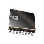
| 供应商器件封装 | 16-TSSOP |
| 其它名称 | ADF4156BRUZ-RL7DKR |
| 分频器/倍频器 | 是/是 |
| 包装 | Digi-Reel® |
| 安装类型 | 表面贴装 |
| 封装/外壳 | 16-TSSOP(0.173",4.40mm 宽) |
| 工作温度 | -40°C ~ 85°C |
| 差分-输入:输出 | 是/无 |
| 标准包装 | 1 |
| 比率-输入:输出 | 2:1 |
| 电压-电源 | 2.7 V ~ 3.3 V |
| 电路数 | 1 |
| 类型 | 分数 N 合成器(RF) |
| 设计资源 | |
| 输入 | CMOS,TTL |
| 输出 | 时钟 |
| 频率-最大值 | 6.2GHz |


- 商务部:美国ITC正式对集成电路等产品启动337调查
- 曝三星4nm工艺存在良率问题 高通将骁龙8 Gen1或转产台积电
- 太阳诱电将投资9.5亿元在常州建新厂生产MLCC 预计2023年完工
- 英特尔发布欧洲新工厂建设计划 深化IDM 2.0 战略
- 台积电先进制程称霸业界 有大客户加持明年业绩稳了
- 达到5530亿美元!SIA预计今年全球半导体销售额将创下新高
- 英特尔拟将自动驾驶子公司Mobileye上市 估值或超500亿美元
- 三星加码芯片和SET,合并消费电子和移动部门,撤换高东真等 CEO
- 三星电子宣布重大人事变动 还合并消费电子和移动部门
- 海关总署:前11个月进口集成电路产品价值2.52万亿元 增长14.8%


PDF Datasheet 数据手册内容提取
6.2 GHz Fractional-N Frequency Synthesizer Data Sheet ADF4156 FEATURES GENERAL DESCRIPTION RF bandwidth to 6.2 GHz The ADF4156 is a 6.2 GHz fractional-N frequency synthesizer 2.7 V to 3.3 V power supply that implements local oscillators in the upconversion and down- Separate V pin allows extended tuning voltage P conversion sections of wireless receivers and transmitters. It Programmable fractional modulus consists of a low noise digital phase frequency detector (PFD), a Programmable charge-pump currents precision charge pump, and a programmable reference divider. 3-wire serial interface There is a Σ-Δ based fractional interpolator to allow programmable Digital lock detect fractional-N division. The INT, FRAC, and MOD registers define Power-down mode an overall N divider (N = (INT + (FRAC/MOD))). The RF output Pin compatible with ADF4110/ADF4111/ADF4112/ADF4113, phase is programmable for applications that require a particular ADF4106, ADF4153, and ADF4154 frequency synthesizers phase relationship between the output and the reference. The Programmable RF output phase ADF4156 also features cycle slip reduction circuitry, leading Loop filter design possible with ADIsimPLL to faster lock times without the need for modifications to the Cycle slip reduction for faster lock times loop filter. APPLICATIONS Control of all on-chip registers is via a simple 3-wire interface. CATV equipment The device operates with a power supply ranging from 2.7 V to Base stations for mobile radio (WiMAX, GSM, PCS, DCS, 3.3 V and can be powered down when not in use. SuperCell 3G, CDMA, WCDMA) Wireless handsets (GSM, PCS, DCS, CDMA, WCDMA) Wireless LANs, PMR Communications test equipment FUNCTIONAL BLOCK DIAGRAM AVDD DVDD VP RSET ADF4156 5-BIT REFERENCE REFIN DOU×B2LER R-COUNTER /2 DIVIDER + PHASE FREQUENCY CHARGE CP VDD –DETECTOR PUMP HIGH Z DGND CSR LOCK CURRENT DETECT SETTING MUXOUT OUMTUPXUT SDOUT VDD RFCP4RFCP3RFCP2RFCP1 RDIV RFINA NDIV N-COUNTER RFINB THIRD-ORDER FRACTIONAL CE INTERPOLATOR CLOCK 32-BIT FRACTION MODULUS INTEGER DATA DATA REG REG REG LE REGISTER AGND DGND CPGND 05863-001 Figure 1. Rev. E Document Feedback Information furnished by Analog Devices is believed to be accurate and reliable. However, no responsibility is assumed by Analog Devices for its use, nor for any infringements of patents or other One Technology Way, P.O. Box 9106, Norwood, MA 02062-9106, U.S.A. rights of third parties that may result from its use. Specifications subject to change without notice. No license is granted by implication or otherwise under any patent or patent rights of Analog Devices. Tel: 781.329.4700 ©2006–2013 Analog Devices, Inc. All rights reserved. Trademarks and registered trademarks are the property of their respective owners. Technical Support www.analog.com
ADF4156 Data Sheet TABLE OF CONTENTS Features .............................................................................................. 1 Register Maps .................................................................................. 10 Applications ....................................................................................... 1 FRAC/INT Register, R0 ............................................................. 11 General Description ......................................................................... 1 Phase Register, R1 ...................................................................... 12 Functional Block Diagram .............................................................. 1 MOD/R Register, R2 .................................................................. 13 Revision History ............................................................................... 2 Function Register, R3 ................................................................. 15 Specifications ..................................................................................... 3 CLK DIV Register, R4 ................................................................ 16 Timing Specifications .................................................................. 4 Reserved Bits ............................................................................... 16 Absolute Maximum Ratings ............................................................ 5 Initialization Sequence .............................................................. 16 Thermal Impedance ..................................................................... 5 RF Synthesizer: A Worked Example ........................................ 17 ESD Caution .................................................................................. 5 Modulus ....................................................................................... 17 Pin Configurations and Function Descriptions ........................... 6 Reference Doubler and Reference Divider ............................. 17 Typical Performance Characteristics ............................................. 7 12-Bit Programmable Modulus ................................................ 17 Circuit Description ........................................................................... 8 Fast Lock Times with the ADF4156 ........................................ 17 Reference Input Section ............................................................... 8 Spur Mechanisms ....................................................................... 19 RF Input Stage ............................................................................... 8 Spur Consistency and Fractional Spur Optimization ........... 19 RF INT Divider ............................................................................. 8 Phase Resync ............................................................................... 20 INT, FRAC, MOD, and R Relationship ..................................... 8 Low Frequency Applications .................................................... 20 RF R-Counter ................................................................................ 8 Filter Design—ADIsimPLL ....................................................... 20 Phase Frequency Detector (PFD) and Charge Pump .............. 9 Interfacing ................................................................................... 21 MUXOUT and Lock Detect ........................................................ 9 PCB Design Guidelines for Chip Scale Package .................... 21 Input Shift Registers ..................................................................... 9 Outline Dimensions ....................................................................... 22 Program Modes ............................................................................ 9 Ordering Guide .......................................................................... 22 REVISION HISTORY 10/13—Rev. D. to Rev. E Change to Program Modes Section ................................................ 9 Changes to Table 3 ............................................................................ 5 Changes to Figure 16 ...................................................................... 10 Updated Outline Dimensions ....................................................... 22 Changes to Figure 17 ...................................................................... 11 Changes to Ordering Guide .......................................................... 22 Changes to CSR Enable Section ................................................... 13 3/12—Rev. C to Rev. D Changes to Figure 19 ...................................................................... 14 Changes to Table 1 ............................................................................ 3 Changes to Function Register, R3 Section and Figure 20 ......... 15 Changes to Ordering Guide .......................................................... 22 Changes to 12-Bit Clock Divider Value Section, to 9/11—Rev. B to Rev. C Clock Divider Mode Section, and to Figure 21 .......................... 16 Changes to Noise Characteristics Parameter ................................ 3 Changes to Reference Doubler and Reference Divider Section 4/11—Rev. A to Rev. B and to Fast Lock Times with the ADF4156 Section .................. 17 Changes to Product Title, Features Section and General Added Figure 22 and Figure 23; Renumbered Sequentially ..... 19 Description Section .......................................................................... 1 Change to Phase Resync Section .................................................. 20 Changes to RF Input Frequency RF Parameter, Table 1 ........... 3 Changes to Interfacing Section and to PCB Design Guidelines IN Changes to Figure 4 and Table 5 ..................................................... 6 for Chip Scale Package Section ..................................................... 21 5/09—Rev. 0 to Rev. A Changes to Outline Dimensions .................................................. 23 Added Low Power Sleep Mode Parameter and Changes to Changes to Ordering Guide .......................................................... 23 Endnote 4, Table 1 ............................................................................ 3 5/06—Revision 0: Initial Version Change to Figure 9 Caption ............................................................ 7 Rev. E | Page 2 of 24
Data Sheet ADF4156 SPECIFICATIONS AV = DV = 2.7 V to 3.3 V, V = AV to 5.5 V, AGND = DGND = 0 V, T = T to T , dBm referred to 50 Ω, unless otherwise noted. DD DD P DD A MIN MAX Table 1. Parameter B Version Unit Test Conditions/Comments1 RF CHARACTERISTICS RF Input Frequency (RF ) 0.5/6.2 GHz min/max −10 dBm min to 0 dBm max. For lower frequencies, IN ensure slew rate (SR) > 400 V/µs. REFERENCE CHARACTERISTICS REF Input Frequency 10/250 MHz min/max For f < 10 MHz, use a dc-coupled CMOS-compatible IN square wave, slew rate > 25 V/µs. REF Input Sensitivity 0.4/AV V p-p min/max Biased at AV /2.2 IN DD DD REF Input Capacitance 10 pF max IN REF Input Current ±100 µA max IN PHASE DETECTOR Phase Detector Frequency3 32 MHz max CHARGE PUMP I Sink/Source Programmable. CP High Value 5 mA typ With R = 5.1 kΩ. SET Low Value 312.5 µA typ Absolute Accuracy 2.5 % typ With R = 5.1 kΩ. SET R Range 2.7/10 kΩ min/max SET I Three-State Leakage Current 1 nA typ Sink and source current. CP Matching 2 % typ 0.5 V < V < V − 0.5. CP P I vs. V 2 % typ 0.5 V < V < V − 0.5. CP CP CP P I vs. Temperature 2 % typ V = V/2. CP CP P LOGIC INPUTS V , Input High Voltage 1.4 V min INH V , Input Low Voltage 0.6 V max INL I /I , Input Current ±1 µA max INH INL C , Input Capacitance 10 pF max IN LOGIC OUTPUTS V , Output High Voltage 1.4 V min Open-drain output chosen; 1 kΩ pull-up to 1.8 V. OH V , Output High Voltage V − 0.4 V min CMOS output chosen. OH DD I , Output High Current 100 µA max OH V , Output Low Voltage 0.4 V max I = 500 µA. OL OL POWER SUPPLIES AV 2.7/3.3 V min/max DD DV AV DD DD V AV /5.5 V min/max P DD I 32 mA max 26 mA typical. DD Low Power Sleep Mode 1 µA typ NOISE CHARACTERISTICS Normalized Phase Noise Floor (PN )4 −220 dBc/Hz typ PLL loop BW = 500 kHz. Measured at 100 kHz offset. SYNTH Normalized 1/f Noise (PN )5 −110 dBc/Hz typ 10 kHz offset; normalized to 1 GHz. 1_f Phase Noise Performance6 At VCO output. 5800 MHz Output7 −89 dBc/Hz typ At 5 kHz offset, 25 MHz PFD frequency. 1 Operating temperature for B version: −40°C to +85°C. 2 AC coupling ensures AVDD/2 bias. 3 Guaranteed by design. Sample tested to ensure compliance. 4 The synthesizer phase noise floor is estimated by measuring the in-band phase noise at the output of the VCO and subtracting 20 log(N) (where N is the N divider value) and 10 log(FPFD). PNSYNTH = PNTOT − 10 log(FPFD) − 20 log(N). 5 The PLL phase noise is composed of 1/f (flicker) noise plus the normalized PLL noise floor. The formula for calculating the 1/f noise contribution at an RF frequency, FRF, and at a frequency offset f is given by PN = PN1_f + 10 log(10 kHz/f) + 20 log(FRF/1 GHz). Both the normalized phase noise floor and flicker noise are modeled in ADIsimPLL. 6 The phase noise is measured with the EV-ADF4156SD1Z evaluation board and the Agilent E5500 phase noise system. 7 fREFIN = 100 MHz, fPFD = 25 MHz, offset frequency = 5 kHz, RFOUT = 5800 MHz, N = 232, loop bandwidth = 20 kHz, ICP = 313 µA, and lowest noise mode. Rev. E | Page 3 of 24
ADF4156 Data Sheet TIMING SPECIFICATIONS AV = DV = 2.7 V to 3.3 V, V = AV to 5.5 V, AGND = DGND = 0 V, T = T to T , dBm referred to 50 Ω, unless otherwise noted. DD DD P DD A MIN MAX Table 2. Parameter Limit at T to T (B Version) Unit Test Conditions/Comments MIN MAX t 20 ns min LE setup time 1 t 10 ns min DATA to CLOCK setup time 2 t 10 ns min DATA to CLOCK hold time 3 t 25 ns min CLOCK high duration 4 t 25 ns min CLOCK low duration 5 t 10 ns min CLOCK to LE setup time 6 t 20 ns min LE pulse width 7 Timing Diagram t4 t5 CLOCK t2 t3 DB1 DB0(LSB) DATA DB23(MSB) DB22 DB2 (CONTROLBITC2) (CONTROLBITC1) t7 LE t1 t6 LE 05863-002 Figure 2. Timing Diagram Rev. E | Page 4 of 24
Data Sheet ADF4156 ABSOLUTE MAXIMUM RATINGS T = 25°C, GND = AGND = DGND = 0 V, V = AV = DV , Stresses above those listed under Absolute Maximum Ratings A DD DD DD unless otherwise noted. may cause permanent damage to the device. This is a stress rating only; functional operation of the device at these or any Table 3. other conditions above those indicated in the operational Parameter Rating section of this specification is not implied. Exposure to absolute V to GND −0.3 V to +4 V maximum rating conditions for extended periods may affect DD V to V −0.3 V to +0.3 V device reliability. DD DD V to GND −0.3 V to +5.8 V P This device is a high performance RF integrated circuit with an V to V −0.3 V to +5.8 V P DD ESD rating of <2 kV, and it is ESD sensitive. Proper precautions Digital I/O Voltage to GND −0.3 V to V + 0.3 V DD should be taken for handling and assembly. Analog I/O Voltage to GND −0.3 V to V + 0.3 V DD REF , RF to GND −0.3 V to V + 0.3 V IN IN DD RFINA to RFINB ±600 mV THERMAL IMPEDANCE Operating Temperature Range Industrial (B Version) −40°C to +85°C Table 4. Thermal Impedance Storage Temperature Range −65°C to +125°C Package Type θJA Unit Maximum Junction Temperature 150°C TSSOP 112 °C/W Reflow Soldering LFCSP_VQ (Paddle Soldered) 30.4 °C/W Peak Temperature 260°C Time at Peak Temperature 40 sec ESD CAUTION Maximum Junction Temperature 150°C Rev. E | Page 5 of 24
ADF4156 Data Sheet PIN CONFIGURATIONS AND FUNCTION DESCRIPTIONS PCRTESVPVDDDVDDD 09876 21111 PIN 1 CPGND 1 INDICATOR 15MUXOUT RSET 1 16 VP AGND 2 14LE ADF4156 CP 2 15 DVDD AGND 3 TOP VIEW 13DATA CPGND 3 ADF4156 14 MUXOUT RRFFIINNBA 45 (Not to Scale) 1112CCLEOCK AGND 4 TOPVIEW 13 LE (NottoScale) RFINB 5 12 DATA 678901 DDNDD RRAFEVIFNDIADN 678 11910 CDCEGLONCDK 05863-003 N1 . O TCTHOEENS NEEXCPOTESDEVA DDT OPVAD AGFERDIR MONGDUUNGDNSTD .BE 05863-004 Figure 3. TSSOP Pin Configuration Figure 4. LFCSP Pin Configuration Table 5. Pin Function Descriptions Pin No. TSSOP LFCSP Mnemonic Description 1 19 R Connecting a resistor between this pin and ground sets the maximum charge-pump output current. The SET relationship between I and R is CP SET 25.5 ICPmax= R SET where R = 5.1 kΩ and I = 5 mA. SET CPmax 2 20 CP Charge-Pump Output. When enabled, this pin provides ±I to the external loop filter, which in turn drives CP the external VCO. 3 1 CPGND Charge-Pump Ground. This is the ground return path for the charge pump. 4 2, 3 AGND Analog Ground. This is the ground return path of the prescaler. 5 4 RF B Complementary Input to the RF Prescaler. Decouple this point to the ground plane with a small bypass IN capacitor, typically 100 pF. 6 5 RF A Input to the RF Prescaler. This small-signal input is normally ac-coupled from the VCO. IN 7 6, 7 AV Positive Power Supply for the RF Section. Decoupling capacitors to the digital ground plane should be DD placed as close as possible to this pin. AV has a value of 3 V ± 10%. AV must have the same voltage as DV . DD DD DD 8 8 REF Reference Input. This is a CMOS input with a nominal threshold of V /2 and an equivalent input resistance IN DD of 100 kΩ. This input can be driven from a TTL or CMOS crystal oscillator, or it can be ac-coupled. 9 9, 10 DGND Digital Ground. 10 11 CE Chip Enable. A logic low on this pin powers down the device and puts the charge-pump output into three-state mode. 11 12 CLOCK Serial Clock Input. This serial clock is used to clock in the serial data to the registers. The data is latched into the shift register on the CLOCK rising edge. This input is a high impedance CMOS input. 12 13 DATA Serial Data Input. The serial data is loaded MSB first with the three LSBs serving as the control bits. This input is a high impedance CMOS input. 13 14 LE Load Enable, CMOS Input. When LE is high, the data stored in the shift registers is loaded into one of the five latches. The control bits are used to select the latch. 14 15 MUXOUT Multiplexer Output. This multiplexer output allows either the RF lock detect, the scaled RF, or the scaled reference frequency to be accessed externally. 15 16, 17 DV Positive Power Supply for the Digital Section. Decoupling capacitors to the digital ground plane should be DD placed as close as possible to this pin. DV has a value of 3 V ± 10%. DV must have the same voltage as AV . DD DD DD 16 18 V Charge-Pump Power Supply. This should be greater than or equal to V . In systems where V is 3 V, it can P DD DD be set to 5.5 V and used to drive a VCO with a tuning range of up to 5.5 V. EPAD The exposed pad must be connected to ground. Rev. E | Page 6 of 24
Data Sheet ADF4156 TYPICAL PERFORMANCE CHARACTERISTICS PFD = 25 MHz, loop bandwidth = 20 kHz, reference = 100 MHz, I = 313 μA, phase noise measurements taken on the Agilent E5500 CP phase noise system. 10 6.00 5 5.95 0 CSR ON R (dBm) ––11–055 P=4/5 P=8/9 NCY (GHz)55..9805 E E CSR OFF POW –20 REQU5.80 F –25 5.75 –30 5.70 ––3450 05863-017 5.65 05863-021 0 1 2 3 4 5 6 7 8 9 –100 0 100 200 300 400 500 600 700 800 900 FREQUENCY(GHz) TIME(µs) Figure 5. RF Input Sensitivity Figure 8. Lock Time for 200 MHz Jump, from 5705 MHz to 5905 MHz, with CSR On and Off 0 5.95 LOWNOISEMODE –20 RF=5800.25MHz,PFD=25MHz,N=232, FRAC=2,MOD=200,20kHzLOOPBW,ICP=313µA, 5.90 –40 c/Hz) –60 Hz)5.85 CSR OFF B G OISE (d –80 ENCY (5.80 HASE N––110200 FREQU5.75 P 5.70 –140 CSR ON ––116800 DPZCHSOAB SMINEMTNEVOG9I4RS0AEMT@EE0D53kPVHHCzAO=S–E8E9.R5RdBOcR/H=z0,.73°RMS, 05863-018 55..6650 05863-022 1k 10k 100k 1M 10M 100M –100 0 100 200 300 400 500 600 700 800 900 FREQUENCY(Hz) TIME(µs) Figure 6. Phase Noise and Spurs, Low Noise Mode Figure 9. Lock Time for 200 MHz Jump, from 5905 MHz to 5705 MHz, with CSR On and Off 0 6 LOWSPURMODE –20 RF=5800.25MHz,PFD=25MHz,N=232,FRAC=2, 5 MOD=200,20kHzLOOPBW,ICP=313µA, 4 DSB INTEGRATEDPHASEERROR=1.09°RMS, –40 PHASENOISE@5kHz=–83dBc/Hz,ZCOMMV940ME03VCO 3 c/Hz) –60 2 B E (d –80 mA) 1 E NOIS–100 I(CP –01 S HA–120 –2 P –3 –140 –4 ––116800 05863-019 ––65 05863-020 1k 10k 100k 1M 10M 100M 0 1 2 3 4 5 FREQUENCY(Hz) VCP(V) Figure 7. Phase Noise and Spurs, Low Spur Mode Figure 10. Charge-Pump Output Characteristics (Note that Fractional Spurs Are Removed and Only the Integer Boundary Spur Remains in Low Spur Mode) Rev. E | Page 7 of 24
ADF4156 Data Sheet CIRCUIT DESCRIPTION REFERENCE INPUT SECTION RF INT DIVIDER The reference input stage is shown in Figure 11. While the The RF INT counter allows a division ratio in the PLL feedback device is operating, SW1 and SW2 are usually closed switches counter. Division ratios from 23 to 4095 are allowed. and SW3 is open. When a power-down is initiated, SW3 is INT, FRAC, MOD, AND R RELATIONSHIP closed and SW1 and SW2 are opened. This ensures that the REF pin is not loaded while the device is powered down. The INT, FRAC, and MOD values, in conjunction with the IN R-counter, enable generating output frequencies that are spaced POWER-DOWN CONTROL by fractions of the phase frequency detector (PFD). See the RF Synthesizer: A Worked Example section for more information. NC 100kΩ The RF VCO frequency (RF ) equation is OUT SW2 REFIN NC TO R-COUNTER SW1 BUFFER RFOUT = FPFD × (INT + (FRAC/MOD)) (1) NO SW3 05863-005 where RFOUT is the output frequency of an external voltage- controlled oscillator (VCO). Figure 11. Reference Input Stage F = REF × [(1 + D)/(R × (1 + T))] (2) PFD IN RF INPUT STAGE where: The RF input stage is shown in Figure 12. It is followed by a REF is the reference input frequency. IN two-stage limiting amplifier to generate the current-mode logic D is the REF doubler bit. IN (CML) clock levels needed for the prescaler. T is the REF divide-by-2 bit (0 or 1). IN R is the preset divide ratio of the binary 5-bit programmable BIAS 1.6V reference counter (1 to 32). GENERATOR AVDD INT is the preset divide ratio of the binary 12-bit counter (23 to 4095). 2kΩ 2kΩ MOD is the preset fractional modulus (2 to 4095). FRAC is the numerator of the fractional division (0 to MOD − 1). RFINA RF N-DIVIDER N = INT + FRAC/MOD FROM RF INPUT STAGE TO PFD N-COUNTER RFINB THIRD-ORDER FRACTIONAL INTERPOLATOR AGND 05863-006 RINETG MREOGD VFARLAUCE Figure 12. RF Input Stage 05863-007 Figure 13. RF INT Divider RF R-COUNTER The 5-bit RF R-counter allows the input reference frequency (REFIN) to be divided down to produce the reference clock to the PFD. Division ratios from 1 to 32 are allowed. Rev. E | Page 8 of 24
Data Sheet ADF4156 PHASE FREQUENCY DETECTOR (PFD) AND INPUT SHIFT REGISTERS CHARGE PUMP The ADF4156 digital section includes a 5-bit RF R-counter, The PFD takes inputs from the R-counter and N-counter and a 12-bit RF N-counter, a 12-bit FRAC counter, and a 12-bit produces an output proportional to the phase and frequency modulus counter. Data is clocked into the 32-bit shift register difference between them. Figure 14 is a simplified schematic of the on each rising edge of CLOCK. The data is clocked in MSB first. phase frequency detector. The PFD includes a fixed-delay element Data is transferred from the shift register to one of five latches that sets the width of the antibacklash pulse, which is typically 3 ns. on the rising edge of LE. The destination latch is determined by This pulse ensures that there is no dead zone in the PFD transfer the state of the three control bits (C3, C2, and C1) in the shift function and results in a consistent reference spur level. register. These bits are the three LSBs (DB2, DB1, and DB0), as shown in Figure 2. The truth table for these bits is shown in UP HI D1 Q1 Table 6. Figure 16 shows a summary of how the latches are U1 programmed. +IN CLR1 PROGRAM MODES DELAY U3 CHPUAMRGPE CP Table 6 and Figure 16 through Figure 21 show how to set up the program modes in the ADF4156. Several settings in the ADF4156 are double buffered, including CLR2 DOWN the modulus value, phase value, R-counter value, reference doubler, HI D2 Q2 –IN U2 05863-008 erevfeenrtesn mceu dsitv oidcceu-bry b-e2f,o arned t hceu rpraerntt c saentt uinsge .a T nheiws m vaelaunes ftohra at ntwy oo f the double buffered settings. The new value must first be latched Figure 14. PFD Simplified Schematic into the device by writing to the appropriate register, and then a MUXOUT AND LOCK DETECT new write must be performed on Register R0. For example, after the modulus value is updated, Register R0 must be written to in The output multiplexer on the ADF4156 allows the user to order to ensure that the modulus value is loaded correctly. access various internal points on the chip. The state of MUXOUT is controlled by M4, M3, M2, and M1 (for details, Table 6. C3, C2, and C1 Truth Table see Figure 16). Figure 15 shows the MUXOUT section in block Control Bits diagram form. C3 C2 C1 Register THREE-STATE OUTPUT DVDD 0 0 0 Register R0 DVDD 0 0 1 Register R1 DGND 0 1 0 Register R2 R-DIVIDER OUTPUT 0 1 1 Register R3 N-DIVIDER OUTPUT 1 0 0 Register R4 ANALOG LOCK DETECT MUX CONTROL MUXOUT DIGITAL LOCK DETECT SERIAL DATA OUTPUT CLOCK DIVIDER OUTPUT R-DIVIDER/2 N-DIVIDER/2 DGND 05863-009 Figure 15. MUXOUT Schematic Rev. E | Page 9 of 24
ADF4156 Data Sheet REGISTER MAPS FRAC/INT REGISTER (R0) SERREV-ED MUXOUT CONTROL 12-BIT INTEGER VALUE (INT) 12-BIT FRACTIONAL VALUE (FRAC) COBNITTRSOL DB31 DB30DB29DB28DB27DB26DB25DB24DB23DB22DB21DB20DB19DB18DB17DB16DB15DB14DB13DB12DB11DB10 DB9 DB8 DB7 DB6 DB5 DB4 DB3 DB2 DB1 DB0 0 M4 M3 M2 M1 N12 N11 N10 N9 N8 N7 N6 N5 N4 N3 N2 N1 F12 F11 F10 F9 F8 F7 F6 F5 F4 F3 F2 F1 C3(0)C2(0)C1(0) PHASE REGISTER (R1) RESERVED 12-BIT PHASE VALUE (PHASE)1 COBNITTRSOL DB31DB30DB29DB28DB27DB26DB25DB24DB23DB22DB21DB20DB19DB18DB17DB16DB15DB14DB13DB12DB11DB10 DB9 DB8 DB7 DB6 DB5 DB4 DB3 DB2 DB1 DB0 0 0 0 0 0 0 0 0 0 0 0 0 0 0 0 0 0 P12 P11 P10 P9 P8 P7 P6 P5 P4 P3 P2 P1 C3(0)C2(0)C1(1) MOD/R REGISTER (R2) R E ED ED LE NC1R RESERV NMOOIDSEE CSR EN CSUETRTRIENNGT1 RESERV PRESCA 1RDIV2 REFEREDOUBLE 5-BIT R COUNTER1 12-BIT MODULUS WORD1 COBNITTRSOL DB31DB30DB29DB28DB27DB26DB25DB24DB23DB22DB21DB20DB19DB18DB17DB16DB15DB14DB13DB12DB11DB10 DB9 DB8 DB7 DB6 DB5 DB4 DB3 DB2 DB1 DB0 0 L2 L1 C1 CPI4 CPI3 CPI2 CPI1 0 P1 U2 U1 R5 R4 R3 R2 R1 M12 M11 M10 M9 M8 M7 M6 M5 M4 M3 M2 M1 C3(0)C2(1)C1(0) FUNCTION REGISTER (R3) RESERVED Σ-Δ RESET RESERVED LDP PDPOLARITY PD CP THREE-STATE COUNTERRESET COBNITTRSOL DB31DB30DB29DB28DB27DB26DB25DB24DB23DB22DB21DB20DB19DB18DB17DB16DB15DB14DB13DB12DB11DB10 DB9 DB8 DB7 DB6 DB5 DB4 DB3 DB2 DB1 DB0 0 0 0 0 0 0 0 0 0 0 0 0 0 0 0 0 0 U12 0 0 0 0 0 0 U7 U6 U5 U4 U3 C3(0)C2(1)C1(1) CLK DIV REGISTER (R4) CLK DIV CONTROL RESERVED MODE 12-BIT CLOCK DIVIDER VALUE RESERVED BITS DB31DB30DB29DB28DB27DB26DB25DB24DB23DB22DB21DB20DB19DB18DB17DB16DB15DB14DB13DB12DB11DB10 DB9 DB8 DB7 DB6 DB5 DB4 DB3 DB2 DB1 DB0 0 0 0 0 0 0 0 0 0 0 0 M2 M1 D12 D11 D10 D9 D8 D7 D6 D5 D4 D3 D2 D1 0 0 0 0 C3(1)C2(0)C1(0) 05863-010 1DOUBLE BUFFERED BIT. Figure 16. Register Summary Rev. E | Page 10 of 24
Data Sheet ADF4156 FRAC/INT REGISTER, R0 12-Bit Fractional Value (FRAC) With the control bits (Bits[2:0]) of Register R0 set to 000, the These 12 bits control what is loaded as the FRAC value into on-chip FRAC/INT register is programmed. Figure 17 shows the fractional interpolator. This is part of what determines the the input data format for programming this register. overall feedback division factor. It is also used in Equation 1. The FRAC value must be less than the value loaded into the 12-Bit Integer Value (INT) MOD register. These 12 bits control what is loaded as the INT value. This MUXOUT determines the overall feedback division factor. It is used in Equation 1 (see the INT, FRAC, MOD, and R Relationship The on-chip multiplexer is controlled by DB30, DB29, DB28, section). and DB27 on the ADF4156. See Figure 17 for the truth table. SERREV-ED MUXOUT CONTROL 12-BIT INTEGER VALUE (INT) 12-BIT FRACTIONAL VALUE (FRAC) COBNITTRSOL DB31 DB30DB29DB28DB27DB26DB25DB24DB23DB22DB21DB20DB19DB18DB17DB16DB15DB14DB13DB12DB11DB10 DB9 DB8 DB7 DB6 DB5 DB4 DB3 DB2 DB1 DB0 0 M4 M3 M2 M1 N12 N11 N10 N9 N8 N7 N6 N5 N4 N3 N2 N1 F12 F11 F10 F9 F8 F7 F6 F5 F4 F3 F2 F1 C3(0)C2(0)C1(0) M4 M3 M2 M1 OUTPUT 0 0 0 0 THREE-STATE OUTPUT 00 00 01 10 DDVGDNDD F12 F11 .......... F2 F1 FRACTIONAL VALUE (FRAC) 0 0 1 1 R-DIVIDER OUTPUT 0 0 .......... 0 0 0 0 1 0 0 N-DIVIDER OUTPUT 0 0 .......... 0 1 1 0 1 0 1 ANALOG LOCK DETECT 0 0 .......... 1 0 2 0 1 1 0 DIGITAL LOCK DETECT 0 0 .......... 1 1 3 0 1 1 1 SERIAL DATA OUTPUT . . .......... . . . 1 0 0 0 RESERVED . . .......... . . . 1 0 0 1 RESERVED . . .......... . . . 1 0 1 0 CLOCK DIVIDER 1 1 .......... 0 0 4092 1 0 1 1 RESERVED 1 1 .......... 0 1 4093 1 1 0 0 FAST-LOCK SWITCH 1 1 .......... 1 0 4094 1 1 0 1 R-DIVIDER/2 1 1 ......... 1 1 4095 1 1 1 0 N-DIVIDER/2 1 1 1 1 RESERVED N12 N11 N10 N9 N8 N7 N6 N5 N4 N3 N2 N1 INTEGER VALUE (INT) 0 0 0 0 0 0 0 1 0 1 1 1 23 0 0 0 0 0 0 0 1 1 0 0 0 24 0 0 0 0 0 0 0 1 1 0 0 1 25 0 0 0 0 0 0 0 1 1 0 1 0 26 . . . . . . . . . . . . . . . . . . . . . . . . . . . . . . . . . . . . . . . 1 1 1 1 1 1 1 1 1 1 0 1 4093 1 1 1 1 1 1 1 1 1 1 1 0 4094 1 1 1 1 1 1 1 1 1 1 1 1 4095 05863-011 Figure 17. FRAC/INT Register (R0) Map Rev. E | Page 11 of 24
ADF4156 Data Sheet PHASE REGISTER, R1 See the Phase Resync section for more information. In most applications, the phase relationship between the RF signal and With the control bits (Bits[2:0]) of Register R1 set to 001, the the reference is not important. In such applications, the phase on-chip phase register is programmed. Figure 18 shows the value can be used to optimize the fractional and subfractional input data format for programming this register. spur levels. See the Spur Consistency and Fractional Spur 12-Bit Phase Value Optimization section for more information. These 12 bits control what is loaded as the phase word. The If neither the phase resync nor the spurious optimization word must be less than the MOD value programmed in the functions are being used, it is recommended that the phase MOD/R register (R2). The word is used to program the RF value be set to 1. output phase from 0° to 360° with a resolution of 360°/MOD. RESERVED 12-BITPHASEVALUE(PHASE) COBNITTRSOL DB31DB30DB29DB28DB27DB26DB25DB24DB23DB22DB21DB20DB19DB18DB17DB16DB15DB14DB13DB12DB11DB10 DB9 DB8 DB7 DB6 DB5 DB4 DB3 DB2 DB1 DB0 0 0 0 0 0 0 0 0 0 0 0 0 0 0 0 0 0 P12 P11 P10 P9 P8 P7 P6 P5 P4 P3 P2 P1 C3(0)C2(0)C1(1) P12 P11 .......... P2 P1 PHASEVALUE(PHASE) 0 0 .......... 0 0 0 0 0 .......... 0 1 1(RECOMMENDED) 0 0 .......... 1 0 2 0 0 .......... 1 1 3 . . .......... . . . . . .......... . . . . . .......... . . . 1 1 .......... 0 0 4092 1 1 .......... 0 1 4093 11 11 .................... 11 01 44009945 05863-012 Figure 18. Phase Register (R1) Map Rev. E | Page 12 of 24
Data Sheet ADF4156 MOD/R REGISTER, R2 Operating at CML levels, the prescaler uses the clock from the RF input stage and divides it down for the counters. The prescaler With the control bits (Bits[2:0]) of Register R1 set to 010, the is based on a synchronous 4/5 core. When it is set to 4/5, the on-chip MOD/R register is programmed. Figure 19 shows the maximum RF frequency allowed is 3 GHz. Therefore, when input data format for programming this register. operating the ADF4156 with frequencies greater than 3 GHz, Noise and Spur Mode the prescaler must be set to 8/9. The prescaler limits the INT value as follows: The noise modes on the ADF4156 are controlled by DB30 and DB29 in the MOD/R register. See Figure 19 for the truth table. With P = 4/5, N = 23 MIN The noise modes allow the user to optimize a design either for With P = 8/9, N = 75 MIN improved spurious performance or for improved phase noise RDIV/2 performance. Setting this bit to 1 inserts a divide-by-2 toggle flip-flop When the lowest spur setting is chosen, dither is enabled. This between the R-counter and PFD, which extends the maximum randomizes the fractional quantization noise so that it resembles REF input rate. IN white noise, rather than spurious noise. As a result, the part is optimized for improved spurious performance. This operation Reference Doubler is typically used when the PLL closed-loop bandwidth is wide Setting DB20 to 0 feeds the REF signal directly into the 5-bit IN for fast-locking applications. Wide loop bandwidth is defined as RF R-counter, disabling the doubler. Setting this bit to 1 multiplies a loop bandwidth greater than 1/10 of the RFOUT channel step the REFIN frequency by a factor of 2 before feeding it into the 5-bit resolution (fRES). A wide loop filter does not attenuate the spurs R-counter. When the doubler is disabled, the REFIN falling edge to the same level as a narrow loop bandwidth. is the active edge at the PFD input to the fractional synthesizer. When the doubler is enabled, both the rising and falling edges For best noise performance, use the lowest noise setting option. of REF become active edges at the PFD input. As well as disabling the dither, using the lowest noise setting IN ensures that the charge pump is operating in an optimum When the doubler is enabled and the lowest spur mode is chosen, region for noise performance. This setting is useful if a narrow the in-band phase noise performance is sensitive to the REF IN loop filter bandwidth is available. The synthesizer ensures duty cycle. The phase noise degradation can be as much as 5 dB extremely low noise, and the filter attenuates the spurs. The for REF duty cycles that are outside a 45% to 55% range. The IN typical performance characteristics show the trade-offs in a phase noise is insensitive to the REF duty cycle when the device IN typical WCDMA setup for various noise and spur settings. is in the lowest noise mode and when the doubler is disabled. CSR Enable The maximum allowable REFIN frequency when the doubler is enabled is 30 MHz. Setting this bit to 1 enables cycle slip reduction, which can improve lock times. Note that the signal at the phase frequency 5-Bit R-Counter detector (PFD) must have a 50% duty cycle for cycle slip The 5-bit R-counter allows the input reference frequency reduction to work. The charge-pump current setting must also (REF ) to be divided down to produce the reference clock to IN be set to a minimum value. See the Fast Lock Times section for the phase frequency detector (PFD). Division ratios from more information. Note that CSR cannot be used if the phase 1 to 32 are allowed. detector polarity is set to negative. 12-Bit Interpolator MOD Value Charge-Pump Current Setting This programmable register sets the fractional modulus, which is DB[27:24] set the charge-pump current setting. These bits the ratio of the PFD frequency to the channel step resolution on should be set to the charge-pump current as indicated by the the RF output. Refer to the RF Synthesizer: A Worked Example loop filter design (see Figure 19). section for more information. Prescaler (P/P + 1) The dual-modulus prescaler (P/P + 1), along with the INT, FRAC, and MOD counters, determines the overall division ratio from the RF to the PFD input. IN Rev. E | Page 13 of 24
ADF4156 Data Sheet R E ESERVED NOISE SR EN CURRENT ESERVED RESCALE DIV2 EFERENCOUBLER CONTROL R MODE C SETTING R P R RD 5-BIT R-COUNTER 12-BIT MODULUS WORD BITS DB31DB30DB29DB28DB27DB26DB25DB24DB23DB22DB21DB20DB19DB18DB17DB16DB15DB14DB13DB12DB11DB10 DB9 DB8 DB7 DB6 DB5 DB4 DB3 DB2 DB1 DB0 0 L2 L1 C1 CPI4 CPI3 CPI2 CPI1 0 P1 U2 U1 R5 R4 R3 R2 R1 M12 M11 M10 M9 M8 M7 M6 M5 M4 M3 M2 M1 C3(0)C2(1)C1(0) C1 CRYECDLUEC TSILOINP U1 RDEOFUEBRLEENRCE M12 M11 .......... M2 M1 INTERPOLATORMODULUS(MOD) 0 0 .......... 1 0 2 0 DISABLED 0 DISABLED 0 0 .......... 1 1 3 1 ENABLED1 1 ENABLED . . .......... . . . . . .......... . . . . . .......... . . . L2 L1 NOISE MODE U2 R-DIVIDER 1 1 .......... 0 0 4092 0 0 LOW NOISE MODE 0 DISABLED 1 1 .......... 0 1 4093 0 1 RESERVED 1 ENABLED 1 1 .......... 1 0 4094 1 0 RESERVED 1 1 .......... 1 1 4095 1 1 LOW SPUR MODE P1 PRESCALER 0 4/5 1 8/9 ICP (mA) R5 R4 R3 R2 R1 R-COUNTER DIVIDE RATIO CPI4 CPI3 CPI2 CPI1 5.1kΩ 0 0 0 0 1 1 0 0 0 0 0.31 0 0 0 1 0 2 0 0 0 1 0.63 0 0 0 1 1 3 0 0 1 0 0.94 0 0 1 0 0 4 0 0 1 1 1.25 . . . . . . 0 1 0 0 1.57 . . . . . . 0 1 0 1 1.88 . . . . . . 0 1 1 0 2.19 0 1 1 1 2.5 1 1 1 0 1 29 1 0 0 0 2.81 1 1 1 1 . 30 1 0 0 1 3.13 1 1 1 1 1 31 1 0 1 0 3.44 0 0 0 0 0 32 1 0 1 1 3.75 1 1 0 0 4.06 1 1 0 1 4.38 1 1 1 0 4.69 1CYCLE SLIP REDUC1TION CA1NNOT B1E USED 1IF THE P5H.0ASE DETECTOR POLARITY IS SET TO NEGATIVE. 05863-013 Figure 19. MOD/R Register (R2) Map Rev. E | Page 14 of 24
Data Sheet ADF4156 Phase Detector Polarity FUNCTION REGISTER, R3 DB6 in the ADF4156 sets the phase detector polarity. When the With the control bits (Bits[2:0]) of Register R2 set to 011, the VCO characteristics are positive, this bit should be set to 1. on-chip function register is programmed. Figure 20 shows the When the characteristics are negative, DB6 should be set to 0. input data format for programming this register. Note that the cycle slip reduction function cannot be used if the Counter Reset phase detector polarity is set to negative. DB3 is the counter reset bit for the ADF4156. When this bit is Lock Detect Precision (LDP) set to 1, the synthesizer counters are held in reset. For normal When DB7 is programmed to 0, the digital lock detect is set operation, this bit should be 0. high when the phase error on 40 consecutive phase detector Charge-Pump Three-State cycles is less than 10 ns each. When this bit is programmed to 1, When programmed to 1, DB4 puts the charge pump into three- 40 consecutive phase detector cycles of less than 6 ns each must state mode. This bit should be set to 0 for normal operation. occur before the digital lock detect is set. Power-Down Σ-Δ Reset DB5 on the ADF4156 provides the programmable power-down For most applications, DB14 should be programmed to 0. When mode. Setting this bit to 1 performs a power-down. Setting this DB14 is programmed to 0, the Σ-Δ modulator is reset to its starting bit to 0 returns the synthesizer to normal operation. While in point, or starting phase word, on every write to Register R0. This software power-down mode, the part retains all information in has the effect of producing consistent spur levels. its registers. Only when supplies are removed are the register If it is not required that the Σ-Δ modulator be reset on each contents lost. write to Register R0, DB14 should be set to 1. When a power-down is activated, the following events occur: 1. The synthesizer counters are forced to their load state conditions. 2. The charge pump is forced into three-state mode. 3. The digital lock detect circuitry is reset. 4. The RF input is debiased. IN 5. The input register remains active and capable of loading and latching data. RESERVED Σ-Δ RESET RESERVED LDP PDPOLARITY PD CP THREE-STATE COUNTERRESET COBNITTRSOL DB31DB30DB29DB28DB27DB26DB25DB24DB23DB22DB21DB20DB19DB18DB17DB16DB15DB14DB13DB12DB11DB10 DB9 DB8 DB7 DB6 DB5 DB4 DB3 DB2 DB1 DB0 0 0 0 0 0 0 0 0 0 0 0 0 0 0 0 0 0 U12 0 0 0 0 0 0 U11 U10 U9 U8 U7 C3(0)C2(1)C1(1) U12 Σ-Δ RESET U11 LDP U7 CROESUENTTER 0 ENABLED 0 10ns 0 DISABLED 1 DISABLED 1 6ns 1 ENABLED U10 PD POLARITY 0 NEGATIVE U8 CTHPREE-STATE 1 POSITIVE 0 DISABLED 1 ENABLED U9 POWER-DOWN 01 DENISAABBLLEEDD 05863-014 Figure 20. Function Register (R3) Map Rev. E | Page 15 of 24
ADF4156 Data Sheet CLK DIV REGISTER, R4 RESERVED BITS With the control bits (Bits[2:0]) of Register R3 set to 100, the All reserved bits should be set to 0 for normal operation. on-chip clock divider register (R4) is programmed. Figure 21 INITIALIZATION SEQUENCE shows the input data format for programming this register. After powering up the part, the correct register programming 12-Bit Clock Divider Value sequence is as follows: The 12-bit clock divider value sets the timeout counter for activation of the fast-lock mode or a phase resync. See the Phase 1. CLK DIV register (R4) Resync section for more information. 2. Function register (R3) 3. MOD/R register (R2) Clock Divider Mode 4. Phase register (R1) DB[20:19] control the mode of the clock divider in the ADF4156. 5. FRAC/INT register (R0) These bits should be set to 01 to activate the fast-lock mode, or to 10 to activate a phase resync. In most applications, neither a fast lock nor a phase resync is required. In this case, DB[20:19] should be set to 00. CLK DIV CONTROL RESERVED MODE 12-BIT CLOCKDIVIDERVALUE RESERVED BITS DB31DB30DB29DB28DB27DB26DB25DB24DB23DB22DB21DB20DB19DB18DB17DB16DB15DB14DB13DB12DB11DB10 DB9 DB8 DB7 DB6 DB5 DB4 DB3 DB2 DB1 DB0 0 0 0 0 0 0 0 0 0 0 0 M2 M1 D12 D11 D10 D9 D8 D7 D6 D5 D4 D3 D2 D1 R4 R3 R2 R1 C3(1)C2(0)C1(0) M2 M1 CLK DIV MODE D12 D11 .......... D2 D1 CLOCK DIVIDER VALUE 0 0 CLKDIVOFF 0 0 .......... 0 0 0 0 1 FAST-LOCK MODE 0 0 .......... 0 1 1 1 0 RESYNCTIMERENABLED 0 0 .......... 1 0 2 1 1 RESERVED 0 0 .......... 1 1 3 . . .......... . . . . . .......... . . . . . .......... . . . 1 1 .......... 0 0 4092 1 1 .......... 0 1 4093 11 11 .................... 11 01 44009945 05863-015 Figure 21. CLK DIV Register (R4) Map Rev. E | Page 16 of 24
Data Sheet ADF4156 RF SYNTHESIZER: A WORKED EXAMPLE for the correct operation of the cycle slip reduction (CSR) function. See the Fast Lock Times section for more information. The following equation governs how the synthesizer should be programmed: 12-BIT PROGRAMMABLE MODULUS RF = [INT + (FRAC/MOD)] × [F ] (3) Unlike most other fractional-N PLLs, the ADF4156 allows the user OUT PFD to program the modulus over a 12-bit range. Therefore, several where: configurations of the ADF4156 are possible for an application by RF is the RF frequency output. OUT varying the modulus value, the reference doubler, and the 5-bit INT is the integer division factor. R-counter. FRAC is the fractionality. MOD is the modulus. For example, consider an application that requires 1.75 GHz RF and 200 kHz channel step resolution. The system has a 13 MHz The PFD frequency can be calculated as follows: reference signal. F = REF × [(1 + D)/(R × (1 + T))] (4) PFD IN One possible setup is feeding the 13 MHz directly into the PFD where: and programming the modulus to divide by 65. This results in REF is the reference frequency input. the required 200 kHz resolution. IN D is the RF REF doubler bit. IN Another possible setup is using the reference doubler to create T is the reference divide-by-2 bit, which is set to 0 or 1. 26 MHz from the 13 MHz input signal. The 26 MHz signal is then R is the RF reference division factor. fed into the PFD, which programs the modulus to divide by 130. For example, in a GSM 1800 system, 1.8 GHz RF frequency This setup also results in 200 kHz resolution, but offers superior output (RF ) is required, 13 MHz reference frequency input phase noise performance compared with the previous setup. OUT (REF ) is available, and 200 kHz channel resolution (f ) is IN RES The programmable modulus is also useful for multistandard required on the RF output. applications. If a dual-mode phone requires PDC and GSM MOD = REF /f IN RES 1800 standards, the programmable modulus is a great benefit. MOD = 13 MHz/200 kHz = 65 The PDC requires 25 kHz channel step resolution, whereas GSM 1800 requires 200 kHz channel step resolution. Therefore, from Equation 4, A 13 MHz reference signal can be fed directly into the PFD, and F = [13 MHz × (1 + 0)/1] = 13 MHz (5) PFD the modulus can be programmed to 520 when in PDC mode 1.8 GHz = 13 MHz × (INT + FRAC/65) (6) (13 MHz/520 = 25 kHz). However, the modulus must be reprogrammed to 65 for GSM 1800 operation (13 MHz/65 where INT = 138 and FRAC = 30. = 200 kHz). MODULUS It is important that the PFD frequency remains constant (13 MHz). The choice of modulus (MOD) depends on the reference signal This allows the user to design one loop filter that can be used in (REF ) available and the channel resolution (f ) required at IN RES both setups without running into stability issues. It is the ratio the RF output. For example, a GSM system with 13 MHz REF sets IN of the RF frequency to the PFD frequency that affects the loop the modulus to 65, resulting in the required RF output resolution design. By keeping this relationship constant, the same loop (f ) of 200 kHz (13 MHz/65). With dither off, the fractional spur RES filter can be used in both applications. interval depends on the modulus values chosen. See Table 7 for more information. FAST LOCK TIMES WITH THE ADF4156 REFERENCE DOUBLER AND REFERENCE DIVIDER As mentioned in the Noise and Spur Mode section, the ADF4156 can be optimized for noise performance. However, in fast-locking The on-chip reference doubler allows the input reference signal applications, the loop bandwidth needs to be wide; therefore, to be doubled. This is useful for increasing the PFD comparison the filter does not provide much attenuation of the spurs. frequency, which in turn improves the noise performance of the system. Doubling the PFD frequency usually improves noise There are two methods of achieving a fast lock time for the performance by 3 dB. It is important to note that the PFD cannot ADF4156: using cycle slip reduction or using dynamic bandwidth operate with frequencies greater than 32 MHz due to a limitation switching mode. In both cases, the idea is to keep the loop band- in the speed of the Σ-Δ circuit of the N-divider. width narrow to attenuate spurs while obtaining a fast lock time. The reference divide-by-2 divides the reference signal by 2, Cycle slip reduction mode is the preferred technique because it resulting in a 50% duty cycle PFD frequency. This is necessary does not require modifications to the loop filter or optimization of the timeout counter values and is therefore easier to implement. Rev. E | Page 17 of 24
ADF4156 Data Sheet In most cases, this method also provides faster lock times than The timeout counter in Register R4 defines the period that the the bandwidth switching mode method. In extreme cases, where device is kept in wideband mode. During wideband mode, the cycle slips do not exist in the settling transient, the bandwidth PLL acquires lock faster due to the wider loop filter bandwidth. switching mode can be used. Stability is maintained at the optimal 45° setting due to the use of the extra resistor in the loop filter. Cycle Slip Reduction Mode Cycle slips occur in integer-N/fractional-N synthesizers when When the timeout counter times out, the charge-pump current the loop bandwidth is narrow compared with the PFD frequency. is reduced from the maximum setting to its set current, and the The phase error at the PFD inputs accumulates too fast for the fast-lock switch is deactivated. The device is then in narrow- PLL to correct, and the charge pump temporarily pumps in the band mode, and spurs are attenuated. wrong direction. This slows down the lock time dramatically. To ensure optimum lock time, the timeout counter should be The ADF4156 contains a cycle slip reduction circuit to extend set to time out when the PLL is close to the final frequency. If the linear range of the PFD, allowing faster lock times without the switch is deactivated, a spike in the settling transient will be requiring loop filter changes. observed due to charge insertion from the switch. Because the When the ADF4156 detects that a cycle slip is about to occur, it PLL is in narrow-band mode, this spike can take some time to turns on an extra charge-pump current cell. This either outputs settle out. This is one of the disadvantages of the bandwidth a constant current to the loop filter or removes a constant current switching mode compared with the cycle slip reduction mode. from the loop filter, depending on whether the VCO tuning Fast Lock: An Example voltage needs to increase or decrease to acquire the new frequency. If a PLL has a reference frequency of 13 MHz, a f of 13 MHz, As a result, the linear range of the PFD is increased. Stability is PFD and a required lock time of 50 µs, the PLL is set to wide bandwidth maintained because the current is constant, not pulsed. for 40 µs. If the phase error increases to a point where another cycle slip If the time set for the wide bandwidth is 40 µs, then is likely, the ADF4156 turns on another charge-pump cell. This process continues until the ADF4156 detects that the VCO Fast-Lock Timer Value = Time in Wide Bandwidth × fPFD frequency is beyond the desired frequency. The extra charge-pump Fast-Lock Timer Value = 40 µs × 13 MHz = 520 cells then begin to turn off one by one until they are all turned off and the frequency is settled. Therefore, 520 must be loaded into Bits DB[18:7] of Register R4. The clock divider mode bits (DB[20:19]) in Register R4 must also Up to seven extra charge-pump cells can be turned on. In most be set to 01 to activate this mode. To activate the fast-lock switch applications, this is sufficient to eliminate cycle slips altogether, on the MUXOUT pin, the MUXOUT control bits (DB[30:27]) resulting in much faster lock times. in Register R0 must be set to 1100. Setting Bit DB28 in the MOD/R register (R2) to 1 enables cycle Fast Lock: Loop Filter Topology slip reduction. A 45% to 55% duty cycle is needed on the signal To use fast-lock mode, an extra connection from the PLL to the at the PFD for CSR to operate correctly. Note that CSR cannot loop filter is needed. The damping resistor in the loop filter be used if the phase detector polarity is set to negative; therefore, must be reduced to ¼ of its value while in wide bandwidth a noninverting loop filter topology should be used with CSR. mode. This is required because the charge-pump current is Dynamic Bandwidth Switching Mode increased by 16 while in wide bandwidth mode and stability must be ensured. When the ADF4156 is in fast-lock mode (that The dynamic bandwidth switching mode involves increasing is, when the fast-lock switch is programmed to appear at the the loop filter bandwidth for a set time at the beginning of the MUXOUT pin), the MUXOUT pin is automatically shorted to locking transient. This is achieved by boosting the charge-pump ground. The following two topologies can be used: current from the set value in Register R2 to the maximum setting. To maintain loop stability during this period, it is necessary to • Topology 1: Divide the damping resistor (R1) into two modify the loop filter by adding a switch and resistor. When the values (R1 and R1A) that have a ratio of 1:3 (see Figure 22). new frequency is programmed to the ADF4156 in this mode, three • Topology 2: Connect an extra resistor (R1A) directly from events occur simultaneously to put the device in wideband mode: MUXOUT, as shown in Figure 23. The extra resistor must • A timeout counter is started. be chosen such that the parallel combination of an extra • The charge-pump current is boosted from its set current to resistor and the damping resistor (R1) is reduced to ¼ of the original value of R1 (see Figure 23). the maximum setting. • The fast-lock switch (available via MUXOUT) is activated. Rev. E | Page 18 of 24
Data Sheet ADF4156 ADF4156 R2 In low spur mode (dither enabled), the repeat length is extended CP VCO to 221 cycles, regardless of the value of MOD, which makes the C1 C2 C3 quantization error spectrum look like broadband noise. As a R1 result, the in-band phase noise at the PLL output can be degraded MUXOUT by as much as 10 dB. Therefore, for lowest noise, keeping dither off is a better choice, particularly when the final loop bandwidth is R1A 05863-023 low enough to attenuate even the lowest frequency fractional spur. Integer Boundary Spurs Figure 22. Topology 1—Fast-Lock Loop Filter Topology Another mechanism for fractional spur creation is interactions ADF4156 R2 between the RF VCO frequency and the reference frequency. CP VCO When these frequencies are not integer related (as is the case C1 C2 C3 with fractional-N synthesizers), spur sidebands appear on the VCO output spectrum at an offset frequency that corresponds R1A R1 to the beat note or the difference in frequency between an MUXOUT integer multiple of the reference and the VCO frequency. 05863-024 These spurs are attenuated by the loop filter and are more Figure 23. Topology 2—Fast-Lock Loop Filter Topology noticeable on channels close to integer multiples of the reference, where the difference frequency can be inside the loop SPUR MECHANISMS bandwidth, hence the name integer boundary spurs. This section describes the three spur mechanisms that arise Reference Spurs with a fractional-N synthesizer and how to minimize these spurs in the ADF4156. Reference spurs are generally not a problem in fractional-N synthesizers because the reference offset is far outside the loop Fractional Spurs bandwidth. However, any reference feedthrough mechanism that The fractional interpolator in the ADF4156 is a third-order Σ-Δ bypasses the loop can cause a problem. One such mechanism is modulator with a modulus (MOD) that is programmable to any feedthrough of low levels of switching noise from the on-chip integer value from 2 to 4095. In low spur mode (dither enabled), reference through the RF pin and back to the VCO, resulting IN the minimum allowable value of MOD is 50. The Σ-Δ modulator in reference spur levels as high as −90 dBc. Care should be taken in is clocked at the PFD reference rate (fPFD) that allows PLL output the PCB layout to ensure that the VCO is well separated from the frequencies to be synthesized at a channel step resolution of input reference to avoid a possible feedthrough path on the board. f /MOD. PFD SPUR CONSISTENCY AND FRACTIONAL SPUR In low noise mode (dither off), the quantization noise from the OPTIMIZATION Σ-Δ modulator appears as fractional spurs. The interval between With dither off, the fractional spur pattern due to the quantization spurs is f /L, where L is the repeat length of the code sequence PFD noise of the Σ-Δ modulator also depends on the phase word set in the digital Σ-Δ modulator. For the third-order modulator used as the starting point of the modulator. Setting the Σ-Δ reset bit in the ADF4156, the repeat length depends on the value of MOD, (DB14 in Register R3) to 0 ensures that this starting point is used as listed in Table 7. for the Σ-Δ modulator on every write to Register R0. Table 7. Fractional Spurs with Dither Off The phase word can be varied to optimize the fractional and Repeat subfractional spur levels on any particular frequency. Therefore, Condition Length Spur Interval a look-up table of phase values corresponding to each frequency If MOD is divisible by 2, but not 3 2 × MOD Channel step/2 can be constructed for use when programming the ADF4156. If MOD is divisible by 3, but not 2 3 × MOD Channel step/3 If MOD is divisible by 6 6 × MOD Channel step/6 The evaluation software has a sweep function to sweep the Otherwise MOD Channel step phase word so that the user can observe the spur levels on a spectrum analyzer. If a look-up table is not used, keep the phase word at a constant value to ensure consistent spur levels on a particular frequency. Rev. E | Page 19 of 24
ADF4156 Data Sheet PHASE RESYNC The output of a fractional-N PLL can settle to any MOD phase LE tSYNC offset with respect to the input reference, where MOD is the SYNC fractional modulus. The phase resync feature in the ADF4156 is (Internal) LAST CYCLE SLIP used to produce a consistent output phase offset with respect to the input reference. This is necessary in applications where the FREQUENCY output phase and frequency are important, such as digital beam PLL SETTLES TO INCORRECT PHASE forming. See the Phase Programmability section for information PLL SETTLES TO about how to program a specific RF output phase when using CORRECT PHASE AFTER RESYNC the phase resync feature. PHASE Phase resync is enabled by setting Bits DB[20:19] in Register R4 05863-016 to 10. When phase resync is enabled, an internal timer generates –100 0 100 200 300 400 500 600 700 800 900 1000 sync signals at intervals of t as indicated by the following TIME (µs) SYNC Figure 24. Phase Resync Example formula: t = CLK_DIV_VALUE × MOD × t Phase Programmability SYNC PFD To program a specific RF output phase, change the phase word where: in Register R1. As this word is swept from 0 to MOD, the RF output t is the PFD reference period. PFD phase sweeps over a 360o/MOD range in steps of 360o/MOD. CLK_DIV_VALUE is the decimal value programmed in Bit DB[18:7] of Register R4. This value can be any integer in the LOW FREQUENCY APPLICATIONS range of 1 to 4095. The specification on the RF input is 0.5 GHz minimum; however, MOD is the modulus value programmed in Bit DB[14:3] of lower RF frequencies can be used if the minimum slew rate Register R2. specification of 400 V/µs is met. An appropriate LVDS driver, such When a new frequency is programmed, the second sync pulse as the FIN1001 from Fairchild Semiconductor, can be used to after the LE rising edge is used to resynchronize the output square up the RF signal before it is fed back into the ADF4156 phase to the reference. The t time should be programmed to RF input. SYNC a value that is at least as long as the worst-case lock time. Doing FILTER DESIGN—ADIsimPLL so guarantees that the phase resync occurs after the last cycle A filter design and analysis program is available to help implement slip in the PLL settling transient. the PLL design. Visit www.analog.com/pll for a free download In the example shown in Figure 24, the PFD reference is of the ADIsimPLL™ software. This software designs, simulates, 25 MHz and the MOD value is 125 for a 200 kHz channel and analyzes the entire PLL frequency domain and time domain spacing. Therefore, tSYNC is set to 400 µs by programming response. Various passive and active filter architectures are allowed. CLK_DIV_VALUE to 80. When designing the loop filter, keep the ratio of the PFD frequency to the loop bandwidth >200:1 to attenuate the Σ-Δ modulator noise. Rev. E | Page 20 of 24
Data Sheet ADF4156 INTERFACING The bottom of the chip scale package has a central thermal pad. The thermal pad on the printed circuit board should be at least The ADF4156 has a simple SPI-compatible serial interface for as large as this exposed pad. On the printed circuit board, there writing to the device. CLOCK, DATA, and LE control the data should be a clearance of at least 0.25 mm between the thermal transfer. When latch enable (LE) is high, the 29 bits that have pad and the inner edges of the pad pattern to ensure that shorting been clocked into the input register on each rising edge of serial is avoided. clock are transferred to the appropriate latch. The maximum allowable serial clock rate is 20 MHz. See Figure 2 for the timing Thermal vias can be used on the printed circuit board thermal diagram and Table 6 for the latch truth table. pad to improve thermal performance of the package. If vias are used, they should be incorporated in the thermal pad on a 1.2 mm PCB DESIGN GUIDELINES FOR CHIP SCALE pitch grid. The via diameter should be between 0.3 mm and PACKAGE 0.33 mm, and the via barrel should be plated with 1 oz of The lands on the lead frame chip scale package (CP-20-6) are copper to plug the via. In addition, the printed circuit board rectangular. The printed circuit board pad for these lands should be thermal pad should be connected to AGND. 0.1 mm longer than the package land length and 0.05 mm wider than the package land width. The package land should be centered on the pad to ensure that the solder joint size is maximized. Rev. E | Page 21 of 24
ADF4156 Data Sheet OUTLINE DIMENSIONS 5.10 5.00 4.90 16 9 4.50 6.40 4.40 BSC 4.30 1 8 PIN 1 1.20 MAX 0.15 0.20 0.05 0.09 0.75 0.30 8° 0.60 B0.S6C5 0.19 SPELAANTIENG 0° 0.45 COPLANARITY 0.10 COMPLIANT TO JEDEC STANDARDS MO-153-AB Figure 25. 16-Lead Thin Shrink Small Outline Package [TSSOP] (RU-16) Dimensions shown in millimeters 4.10 0.30 4.00SQ 0.25 PIN1 3.90 0.18 INDICATOR PIN1 16 20 INDICATOR 0.50 BSC 15 1 EXPOSED 2.30 PAD 2.10SQ 2.00 11 5 0.65 10 6 0.20MIN TOPVIEW 0.60 BOTTOMVIEW 0.55 0.80 FORPROPERCONNECTIONOF 0.75 THEEXPOSEDPAD,REFERTO 0.05MAX THEPINCONFIGURATIONAND 0.70 0.02NOM FUNCTIONDESCRIPTIONS SECTIONOFTHISDATASHEET. COPLANARITY SEATING 0.08 PLANE COMPLIANTTOJED0E.2C0SRTEAFNDARDSMO-220-WGGD-1. 08-16-2010-B Figure 26. 20-Lead Lead Frame Chip Scale Package [LFCSP_WQ] 4 mm × 4 mm Body, Very Very Thin Quad (CP-20-6) Dimensions shown in millimeters ORDERING GUIDE Model1 Temperature Range Package Description Package Option ADF4156BRUZ −40°C to +85°C 16-Lead Thin Shrink Small Outline Package [TSSOP] RU-16 ADF4156BRUZ-RL −40°C to +85°C 16-Lead Thin Shrink Small Outline Package [TSSOP] RU-16 ADF4156BRUZ-RL7 −40°C to +85°C 16-Lead Thin Shrink Small Outline Package [TSSOP] RU-16 ADF4156BCPZ −40°C to +85°C 20-Lead Lead Frame Chip Scale Package [LFCSP_WQ] CP-20-6 ADF4156BCPZ-RL −40°C to +85°C 20-Lead Lead Frame Chip Scale Package [LFCSP_WQ] CP-20-6 ADF4156BCPZ-RL7 −40°C to +85°C 20-Lead Lead Frame Chip Scale Package [LFCSP_WQ] CP-20-6 EV-ADF4156SD1Z Evaluation Board 1 Z = RoHS Compliant Part. Rev. E | Page 22 of 24
Data Sheet ADF4156 NOTES Rev. E | Page 23 of 24
ADF4156 Data Sheet NOTES I2C refers to a communications protocol originally developed by Philips Semiconductors (now NXP Semiconductors). ©2006–2013 Analog Devices, Inc. All rights reserved. Trademarks and registered trademarks are the property of their respective owners. D05863-0-10/13(E) Rev. E | Page 24 of 24
Mouser Electronics Authorized Distributor Click to View Pricing, Inventory, Delivery & Lifecycle Information: A nalog Devices Inc.: EV-ADF4156SD1Z ADF4156BCPZ ADF4156BRUZ-RL7 ADF4156BCPZ-RL ADF4156BRUZ ADF4156BRUZ-RL ADF4156BCPZ-RL7