ICGOO在线商城 > 集成电路(IC) > PMIC - 稳压器 - DC DC 开关稳压器 > TPS62122DRVR
 Datasheet下载
- 型号: TPS62122DRVR
- 制造商: Texas Instruments
- 库位|库存: xxxx|xxxx
- 要求:
| 数量阶梯 | 香港交货 | 国内含税 |
| +xxxx | $xxxx | ¥xxxx |
查看当月历史价格
查看今年历史价格
TPS62122DRVR产品简介:
ICGOO电子元器件商城为您提供TPS62122DRVR由Texas Instruments设计生产,在icgoo商城现货销售,并且可以通过原厂、代理商等渠道进行代购。 TPS62122DRVR价格参考。Texas InstrumentsTPS62122DRVR封装/规格:PMIC - 稳压器 - DC DC 开关稳压器, 可调式 降压 开关稳压器 IC 正 1.2V 1 输出 75mA 6-WDFN 裸露焊盘。您可以下载TPS62122DRVR参考资料、Datasheet数据手册功能说明书,资料中有TPS62122DRVR 详细功能的应用电路图电压和使用方法及教程。
TPS62122DRVR是由Texas Instruments(德州仪器)生产的PMIC(电源管理集成电路),具体分类为DC-DC开关稳压器。该型号的主要应用场景包括:

1. 便携式电子设备:如智能手机、平板电脑、可穿戴设备等,这些设备对电源效率和体积要求较高。TPS62122DRVR具有高效能和小尺寸的特点,能够满足这些设备的电源管理需求。

2. 低功耗系统:适用于需要长时间运行且功耗敏感的应用,如物联网(IoT)设备、传感器节点、无线通信模块等。它能够在轻载条件下保持高效率,延长电池寿命。

3. 工业控制与自动化:用于工业控制器、PLC(可编程逻辑控制器)、数据采集系统等。这些应用通常需要稳定可靠的电源供应,TPS62122DRVR具备良好的负载瞬态响应和稳定性,确保系统的正常运行。

4. 医疗设备:如便携式医疗监测设备、血糖仪、心率监测仪等。这些设备不仅要求电源高效可靠,还需要符合严格的医疗标准。TPS62122DRVR的低噪声和高精度输出特性使其成为理想选择。

5. 消费类电子产品:如数码相机、智能手表、蓝牙耳机等。这类产品通常需要紧凑的设计和高效的电源管理,TPS62122DRVR的小封装和高效性能正好满足这些需求。

6. 汽车电子:在车载信息娱乐系统、导航设备、高级驾驶辅助系统(ADAS)中,TPS62122DRVR可以提供稳定的电源输出,同时具备良好的抗电磁干扰能力,确保系统在复杂环境下的可靠性。

总的来说,TPS62122DRVR凭借其高效能、小尺寸、低噪声和高可靠性等特点,广泛应用于各种对电源管理和效率有严格要求的领域,尤其适合便携式和低功耗设备。
| 参数 | 数值 |
| 产品目录 | 集成电路 (IC)半导体 |
| 描述 | IC REG BUCK SYNC ADJ 75MA 6SON稳压器—开关式稳压器 15V75mA96% Eff Step-Down Converter |
| DevelopmentKit | TPS62122EVM-586 |
| 产品分类 | |
| 品牌 | Texas Instruments |
| 产品手册 | |
| 产品图片 |
|
| rohs | 符合RoHS无铅 / 符合限制有害物质指令(RoHS)规范要求 |
| 产品系列 | 电源管理 IC,稳压器—开关式稳压器,Texas Instruments TPS62122DRVR- |
| 数据手册 | |
| 产品型号 | TPS62122DRVR |
| PCN设计/规格 | |
| PWM类型 | - |
| 产品种类 | 稳压器—开关式稳压器 |
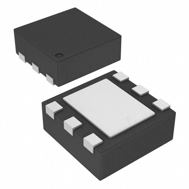
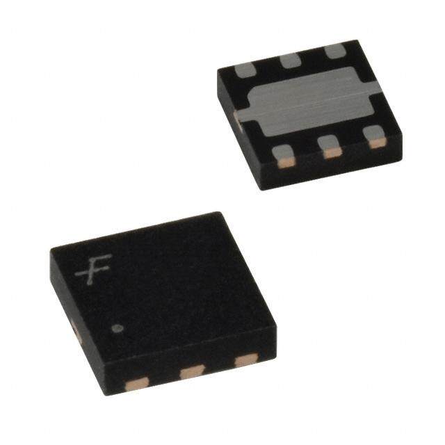
| 供应商器件封装 | 6-SON(2x2) |
| 关闭 | Shutdown |
| 其它名称 | 296-27695-1 |
| 包装 | 剪切带 (CT) |
| 同步整流器 | 是 |
| 商标 | Texas Instruments |
| 安装类型 | 表面贴装 |
| 安装风格 | SMD/SMT |
| 封装 | Reel |
| 封装/外壳 | 6-WDFN 裸露焊盘 |
| 封装/箱体 | WSON-6 |
| 工作温度 | -40°C ~ 85°C |
| 工作温度范围 | - 40 C to + 85 C |
| 工厂包装数量 | 3000 |
| 开关频率 | 800 kHz |
| 拓扑结构 | Buck |
| 最大工作温度 | + 85 C |
| 最大输入电压 | 15 V |
| 最小工作温度 | - 40 C |
| 最小输入电压 | 2 V |
| 标准包装 | 1 |
| 电压-输入 | 2 V ~ 15 V |
| 电压-输出 | 1.2 V ~ 5.5 V |
| 电流-输出 | 75mA |
| 电源电压-最小 | 2 V |
| 电源电流 | 11 uA |
| 类型 | 降压(降压) |
| 系列 | TPS62122 |
| 输入电压 | 2 V to 15 V |
| 输出数 | 1 |
| 输出电压 | 5.5 V |
| 输出电流 | 75 mA |
| 输出端数量 | 1 Output |
| 输出类型 | 可调式 |
| 配用 | /product-detail/zh/TPS62122EVM-586/296-35042-ND/2696899 |
| 频率-开关 | 最高 800kHz |


.jpg)

- 商务部:美国ITC正式对集成电路等产品启动337调查
- 曝三星4nm工艺存在良率问题 高通将骁龙8 Gen1或转产台积电
- 太阳诱电将投资9.5亿元在常州建新厂生产MLCC 预计2023年完工
- 英特尔发布欧洲新工厂建设计划 深化IDM 2.0 战略
- 台积电先进制程称霸业界 有大客户加持明年业绩稳了
- 达到5530亿美元!SIA预计今年全球半导体销售额将创下新高
- 英特尔拟将自动驾驶子公司Mobileye上市 估值或超500亿美元
- 三星加码芯片和SET,合并消费电子和移动部门,撤换高东真等 CEO
- 三星电子宣布重大人事变动 还合并消费电子和移动部门
- 海关总署:前11个月进口集成电路产品价值2.52万亿元 增长14.8%


PDF Datasheet 数据手册内容提取
Product Sample & Technical Tools & Support & Reference Folder Buy Documents Software Community Design TPS62120,TPS62122 SLVSAD5A–JULY2010–REVISEDAUGUST2015 TPS6212x 15-V, 75-mA Highly Efficient Buck Converter 1 Features The wide operating input voltage range of 2 V to 15 V supports energy harvesting, battery powered and as • WideInputVoltageRange:2Vto15V 1 well9-Vor12-Vlinepoweredapplications. • Upto96%Efficiency With its advanced hysteretic control scheme, the • PowerSaveModeWith11-µAQuiescentCurrent converter provides power save mode operation. At • OutputCurrent75mA light loads the converter operates in pulse frequency • OutputVoltageRange:1.2Vto5.5V modulation (PFM) mode and transitions automatically in pulse width modulation (PWM) mode at higher load • Upto800-kHzSwitchFrequency currents. The power save mode maintains high • SynchronousConverter,NoExternalRectifier efficiency over the entire load current range. The • LowOutputRippleVoltage hysteretic control scheme is optimized for low output ripple voltage in PFM mode in order to reduce output • 100%DutyCycleforLowestDropout noise to a minimum. The device consumes only 10- • SmallSOT8-Pin(TPS62120)and2-mm ×2-mm µA quiescent current from VIN in PFM mode DFN6-Pin(TPS62122)Package operation. • InternalSoftStart Inshutdownmode,thedeviceisturnedoff. • PowerGoodOpenDrainOutput(TPS62120) An open-drain power good output is available in the • Open-DrainOutputforOutputDischarge TPS62120 and indicates once the output voltage is in (TPS62120) regulation. • 2.5-VRisingand1.85-VFallingUVLOThresholds The TPS62120 has an additional SGND pin which is connected to GND during shutdown mode. This 2 Applications outputcanbeusedtodischargetheoutputcapacitor. • LowPowerRFApplications The TPS6212x operates over an free air temperature • UltraLowPowerMicroprocessors range of –40°C to 85°C. The TPS62120 is available • EnergyHarvesting in a small 8-pin SOT-23 package and the TPS62122 ina2mm× 2mm6-pinDFNpackage. • IndustrialMeasuring DeviceInformation(1) 3 Description PARTNUMBER PACKAGE BODYSIZE(NOM) The TPS6212x device is a highly efficient synchronous step-down DC-DC converter optimized TPS62120 SOT-23(8) 2.90mm×1.63mm for low-power applications. The device supports up to TPS62122 SON(6) 2.00mm×2.00mm 75-mA output current and allows the use of tiny (1) For all available packages, see the orderable addendum at externalinductorsandcapacitors. theendofthedatasheet. TypicalApplicationSchematic EfficiencyvsOutputCurrent VOUT= 1.8 V 100 VIN= 2.5 V to 15 V TPS62120 L22mH up to 75 mA VIN= 5.5 V VIN SW 90 R1 VIN= 8 V 4.7CmINF EGNND FB 30204 0k WkRW2 C22ff pF C4.O7UmTF Efficiency - % 678000 VIN= 15 V VIN= 12 VVIN= 10 V VOUT 50 SGND Rpullup 100kW VLO= =1 85 mVH,, PG PWR GOOD 40 LPS3015, CO= 4.7mF 30 0.1 1 10 100 IO- Output Current - mA 1 An IMPORTANT NOTICE at the end of this data sheet addresses availability, warranty, changes, use in safety-critical applications, intellectualpropertymattersandotherimportantdisclaimers.PRODUCTIONDATA.
TPS62120,TPS62122 SLVSAD5A–JULY2010–REVISEDAUGUST2015 www.ti.com Table of Contents 1 Features.................................................................. 1 8.4 DeviceFunctionalModes........................................10 2 Applications........................................................... 1 9 ApplicationandImplementation........................ 12 3 Description............................................................. 1 9.1 ApplicationInformation............................................12 4 RevisionHistory..................................................... 2 9.2 TypicalApplications................................................12 9.3 SystemExamples...................................................20 5 DeviceComparisonTable..................................... 3 10 PowerSupplyRecommendations..................... 22 6 PinConfigurationandFunctions......................... 3 11 Layout................................................................... 22 7 Specifications......................................................... 4 11.1 LayoutGuidelines.................................................22 7.1 AbsoluteMaximumRatings......................................4 11.2 LayoutExamples...................................................22 7.2 ESDRatings..............................................................4 12 DeviceandDocumentationSupport................. 24 7.3 RecommendedOperatingConditions.......................4 7.4 ThermalInformation..................................................5 12.1 DeviceSupport......................................................24 7.5 ElectricalCharacteristics...........................................5 12.2 RelatedLinks........................................................24 7.6 TypicalCharacteristics..............................................7 12.3 CommunityResources..........................................24 12.4 Trademarks...........................................................24 8 DetailedDescription.............................................. 8 12.5 ElectrostaticDischargeCaution............................24 8.1 Overview...................................................................8 12.6 Glossary................................................................24 8.2 FunctionalBlockDiagram.........................................8 13 Mechanical,Packaging,andOrderable 8.3 FeatureDescription...................................................9 Information........................................................... 24 4 Revision History NOTE:Pagenumbersforpreviousrevisionsmaydifferfrompagenumbersinthecurrentversion. ChangesfromOriginal(July2010)toRevisionA Page • AddedPinConfigurationandFunctionssection,HandlingRatingtable,FeatureDescriptionsection,Device FunctionalModes,ApplicationandImplementationsection,PowerSupplyRecommendationssection,Layout section,DeviceandDocumentationSupportsection,andMechanical,Packaging,andOrderableInformation section ................................................................................................................................................................................... 1 2 SubmitDocumentationFeedback Copyright©2010–2015,TexasInstrumentsIncorporated ProductFolderLinks:TPS62120 TPS62122
TPS62120,TPS62122 www.ti.com SLVSAD5A–JULY2010–REVISEDAUGUST2015 5 Device Comparison Table PARTNUMBER ACTIVEDISCHARGESWITCH POWERGOOD V OUT TPS62120(1) yes Open-Drain adjustable TPS62122(2) no no adjustable (1) TheDCNpackageisavailableintapeonreel.AddRsuffixtoorderquantitiesof3000partsperreel,Tsuffixfor250partsperreel. (2) TheDRVpackageisavailableintapeonreel.AddRsuffixtoorderquantitiesof3000partsperreel,Tsuffixfor250partsperreel. 6 Pin Configuration and Functions DRVPackage 6-PinSON TopView VOSUWT 21 EXPROSMEALDPAD 56 VGINND HE FB 3 T 4 EN DCNPackage 8-PinSOT-23 TopView VIN 1 8 VOUT GND 2 7 SW EN 3 6 PG SGND 4 5 FB PinFunctions PIN I/O DESCRIPTION NAME DFN SOT-23 EN 4 3 I Pullingthispintohighactivatesthedevice.Lowlevelshutsitdown.Thispinmustbeterminated. FB 3 5 I Thisisthefeedbackpinfortheregulator.Connectexternalresistor-dividertothispin. GND 6 2 PWR GNDsupplypin. ThispinisavailableinTPS62120only. PG — 6 O Open-drainpowergoodoutput.Connectthisterminalthroughapullupresistortoavoltagerailup to5.5Vorleaveitopen.Thispincansink500µA. ThispinisavailableinTPS62120only. Open-drainoutputwhichisturnedonduringshutdownmode(EN=0)orVINisbelowtheUVLO threshold.TheoutputconnectstheSGNDpintoGNDthroughaninternalMOSFETwithtypical SGND — 4 I 370-ΩR .Whenthedeviceisenabled(EN=1),thisoutputishighimpedance.Todischarge DS(ON) theoutputcapacitorduringshutdownmode,connectthispintoVOUT(outputcapacitor)orleaveit open. ThisistheswitchpinandisconnectedtotheinternalMOSFETswitches.Connecttheinductorto SW 1 7 O thisterminal.DonottiethispintoVIN,VOUTorGND. VIN 5 1 PWR V powersupplypin. IN VOUT 2 8 I Thispinmustbeconnectedtotheoutputcapacitor. Exposed — Thermal — — ExposedthermalpadavailableonlyinDRVpackageoption.ThispadmustbeconnectedtoGND. Pad Copyright©2010–2015,TexasInstrumentsIncorporated SubmitDocumentationFeedback 3 ProductFolderLinks:TPS62120 TPS62122
TPS62120,TPS62122 SLVSAD5A–JULY2010–REVISEDAUGUST2015 www.ti.com 7 Specifications 7.1 Absolute Maximum Ratings Overoperatingfree-airtemperaturerange(unlessotherwisenoted)(1) MIN MAX UNIT VoltageatVIN(2) –0.3 17 V VoltageatSW dynamicallyduringswitchingt<10µs 17 V PIN staticDC –0.3 6 VI VoltageatENPIN(2) VIN+0.3, –0.3 V but≤17 VoltageonFBPin –0.3 3.6 V VoltageatPG,VOUT,SGND(2) –0.3 6 V I CurrentintoPGpin 0.5 mA IN Maximumoperatingjunctiontemperature,T –40 125 °C J Storagetemperature,T –65 150 °C stg (1) StressesbeyondthoselistedunderAbsoluteMaximumRatingsmaycausepermanentdamagetothedevice.Thesearestressratings onlyandfunctionaloperationofthedeviceattheseoranyotherconditionsbeyondthoseindicatedunderRecommendedOperating Conditionsisnotimplied.Exposuretoabsolute-maximum-ratedconditionsforextendedperiodsmayaffectdevicereliability. (2) AllvoltagevaluesarewithrespecttonetworkgroundterminalGND. 7.2 ESD Ratings VALUE UNIT Humanbodymodel(HBM),perANSI/ESDA/JEDECJS-001(1) ±2000 V Electrostaticdischarge V (ESD) Chargeddevicemodel(CDM),perJEDECspecificationJESD22-C101(2) ±1000 (1) JEDECdocumentJEP155statesthat500-VHBMallowssafemanufacturingwithastandardESDcontrolprocess. (2) JEDECdocumentJEP157statesthat250-VCDMallowssafemanufacturingwithastandardESDcontrolprocess. 7.3 Recommended Operating Conditions MIN NOM MAX UNIT SupplyvoltageVIN,deviceinoperation 2 15 V V =2V,V =1.8V,DCR =0.7Ω 25 IN OUT L Outputcurrentcapability mA V ≥2.5V,V =1.8V,DCR =0.7Ω 75 IN OUT L Effectiveinductance 10 22 33 µH Effectiveoutputcapacitance 1.0 2 33 µF Outputvoltage 1.2 5.5 V OperatingambienttemperatureT (1),(unlessotherwisenoted) –40 85 °C A Operatingjunctiontemperature,T –40 125 °C J (1) Inapplicationswherehighpowerdissipationand/orpoorpackagethermalresistanceispresent,themaximumambienttemperaturemay havetobederated.Maximumambienttemperature(T )isdependentonthemaximumoperatingjunctiontemperature(T ),the A(max) J(max) maximumpowerdissipationofthedeviceintheapplication(P ),andthejunction-to-ambientthermalresistanceofthepart/package D(max) intheapplication(R ),asgivenbythefollowingequation:T =T –(R ×P ). θJA A(max) J(max) θJA D(max) 4 SubmitDocumentationFeedback Copyright©2010–2015,TexasInstrumentsIncorporated ProductFolderLinks:TPS62120 TPS62122
TPS62120,TPS62122 www.ti.com SLVSAD5A–JULY2010–REVISEDAUGUST2015 7.4 Thermal Information TPS62120 TPS62122 THERMALMETRIC(1) DCN[SOT-23] DRV[DFN] UNIT 8PINS 6PINS R Junction-to-ambientthermalresistance 259.7 114.4 °C/W θJA R Junction-to-case(top)thermalresistance 114.1 73.7 °C/W θJC(top) R Junction-to-boardthermalresistance 185.8 201.9 °C/W θJB ψ Junction-to-topcharacterizationparameter 21.6 0.8 °C/W JT ψ Junction-to-boardcharacterizationparameter 121.6 94.9 °C/W JB R Junction-to-case(bottom)thermalresistance n/a 122.7 °C/W θJC(bot) (1) Formoreinformationabouttraditionalandnewthermalmetrics,seetheSemiconductorandICPackageThermalMetricsapplication report,SPRA953 7.5 Electrical Characteristics V =8V,V =1.8V,EN=V ,T =–40°Cto85°C,typicalvaluesareatT =25°C(unlessotherwisenoted),C =4.7µF, IN OUT IN J J IN L=22µH,C =4.7µF OUT PARAMETER TESTCONDITIONS MIN TYP MAX UNIT SUPPLY V Inputvoltagerange(1) Deviceoperating 2 15 V IN I =0mA,devicenotswitching,EN=VIN, OUT 11 18 regulatorsleeps I Quiescentcurrent µA Q I =0mA,deviceswitching,V =8V,V =1.8 OUT IN OUT 13 V V =5.5V=V ,T =25°C,high-sideMOSFET I Activemodecurrentconsumption IN OUT J 240 275 µA Active switchfullyturnedon I Shutdowncurrent EN=GND,V =SW=0V,V =3.6V (2) 0.3 1.2 µA SD OUT IN FallingV 1.85 1.95 IN V Undervoltagelockoutthreshold V UVLO RisingV 2.5 2.61 IN ENABLE,THRESHOLD V ThresholdfordetectinghighEN 2V≤V ≤15V,risingedge 0.8 1.1 V IHTH IN V ThresholdfordetectinglowEN 2V≤V ≤15V,fallingedge 0.4 0.6 V ILTHHYS IN I Inputbiascurrent,EN EN=GNDorV 0 50 nA IN IN POWERSWITCH V =3.6V 2.3 3.4 IN High-sideMOSFETON-resistance V =8V 1.75 2.5 IN R Ω DS(ON) V =3.6V 1.3 2.5 IN Low-sideMOSFETON-resistance V =8V 1.2 1.75 IN ForwardcurrentlimitMOSFEThigh- I V =8V,openloop 200 250 400 mA LIMF side IN T Thermalshutdown Increasingjunctiontemperature 150 °C SD Thermalshutdownhysteresis Decreasingjunctiontemperature 20 °C REGULATOR t MinimumONtime V =3.6V,V =1.8V 700 ns ONmin IN OUT t MinimumOFFtime V =3.6V,V =1.8V 60 ns OFFmin IN OUT V Internalreferencevoltage 0.8 V REF FeedbackFBvoltagecomparator Referredto0.8-Vinternalreference –2.5% 0% 2.5% V threshold FB FeedbackFBvoltagelineregulation I =50mA (3) 0.04 %/V OUT I InputbiascurrentFB V =0.8V 0 50 nA IN FB (1) Thetypicalrequiredsupplyvoltageforstartupis2.5V.ThepartisfunctionaldowntothefallingUVLO(undervoltagelockout)threshold. (2) ShutdowncurrentintoVINpin,includesinternalleakage. (3) V +1V≤V ;V ≤5.5V OUT IN OUT Copyright©2010–2015,TexasInstrumentsIncorporated SubmitDocumentationFeedback 5 ProductFolderLinks:TPS62120 TPS62122
TPS62120,TPS62122 SLVSAD5A–JULY2010–REVISEDAUGUST2015 www.ti.com Electrical Characteristics (continued) V =8V,V =1.8V,EN=V ,T =–40°Cto85°C,typicalvaluesareatT =25°C(unlessotherwisenoted),C =4.7µF, IN OUT IN J J IN L=22µH,C =4.7µF OUT PARAMETER TESTCONDITIONS MIN TYP MAX UNIT TimefromactiveENtodevicestartsswitching,V = t Regulatorstart-uptime IN 50 150 Start 2.6V µs t Outputvoltageramptime TimetorampupV =1.8V,noload (4) 120 300 Ramp OUT V =V =V =1.8V,EN=GND,devicein I LeakagecurrentintoSWpin OUT IN SW 1 1.5 µA LK_SW shutdownmode POWERGOODOUTPUT(TPS62120) RisingV feedbackvoltage 93% 95% 97% FB V Powergoodthresholdvoltage THPG FallingV feedbackvoltage 87% 90% 93% FB CurrentintoPGpinI=500µA,V >1.5V 165 OUT V Outputlowvoltage mV OL CurrentintoPGpinI=100µA,1.2V<V <1.5V 50 OUT V Outputhighvoltage Opendrainoutput,externalpullupresistor 5.5 V H LeakagecurrentintoPGpin V =1.8V,EN=high,FB=0.85V 0 50 nA (PG) I LKG LeakageintoVOUTpin V =1.8V 0 50 nA (OUT) Internalpowergoodcomparatordelay T V =1.8V 2 5 µs PGDL time OUT SGNDOPENDRAINOUTPUT(TPS62120) R NMOSdrainsourceresistance SGND=1.8V,V =2V 370 Ω DS(ON) IN I LeakagecurrentintoSGNDpin EN=VIN,SGND=1.8V 0 50 nA LKG (4) Maximumvaluenotproductiontested. 6 SubmitDocumentationFeedback Copyright©2010–2015,TexasInstrumentsIncorporated ProductFolderLinks:TPS62120 TPS62122
TPS62120,TPS62122 www.ti.com SLVSAD5A–JULY2010–REVISEDAUGUST2015 7.6 Typical Characteristics 3.5 20 18 3 W ce - TA= 85°C 16 TA= 85°C witch Resistan 2.25 TA= 60T°AC= 2T5A°C= -40°C nt current -Am 111024 TTAA== 6205°°CC side S 1.5 uiesce 8 on - Low 1 Iq - Q 6 TA= -40°C Device enabled and S 4 UVLO rising threshold RD 0.5 has been tripped 2 0 0 0 2 4 6 8 10 12 14 16 0 2 4 6 8 10 12 14 16 VI- Input Voltage - V VI- Input Voltage - V Figure1.Low-SideSwitchResistanceRDS(ON)vsVIN Figure2.QuiescentCurrentvsVIN 1.8 900 VOUT= 2 V, VIN= 7 V 1.6 TA= 85°C 800 L= 18mH LPS3015, COUT= 4.7mF A 1.4 700 m own Current - 1.12 TTAA== 6205°°CC cy - kHz 560000 VIN= 3 V VIN= 5 V VIN= 12V VIN= 9 V d n I- ShutSD00..68 TA= -40°C f - Freque 340000 VIN= 15 V 0.4 200 0.2 100 0 0 0 2 4 6 8 10 12 14 16 0 10 20 30 40 50 60 70 80 VI- Input Voltage - V IO- Output Current - mA Figure3.ShutdownCurrentvsVIN Figure4.SwitchFrequencyvsOutputCurrentIOUT (V =2V) OUT 900 900 VOUT= 3.3 V, VIN= 9 V VOUT= 5.0 V, 800 LCO=U 2T2=m H4. 7 LmQFH3NPN, VIN= 7 V 800 LCO=U 1T8=m H4. 7LPmFS3015, VIN= 12 V 700 700 VIN= 5 V 600 600 VIN= 9 V Hz Hz y - k 500 VIN= 12 V y - k500 VIN= 7 V c c n n e e f - Frequ 340000 VIN= 15 V f - Frequ340000 200 200 VIN= 15 V 100 100 0 0 0 10 20 30 40 50 60 70 80 0 10 20 30 40 50 60 70 80 IO- Output Current - mA IO- Output Current - mA Figure5.SwitchFrequencyvsOutputCurrentIOUT Figure6.SwitchFrequencyvsOutputCurrentIOUT (VOUT=3.3V) (VOUT=5V) Copyright©2010–2015,TexasInstrumentsIncorporated SubmitDocumentationFeedback 7 ProductFolderLinks:TPS62120 TPS62122
TPS62120,TPS62122 SLVSAD5A–JULY2010–REVISEDAUGUST2015 www.ti.com 8 Detailed Description 8.1 Overview The TPS6212x synchronous step-down converter family uses an unique hysteretic PFM/PWM controller scheme which enables switching frequencies of up to 800 kHz, excellent transient response and AC load regulation at operationwithsmalloutputcapacitors. At high load currents the converter operates in quasi fixed frequency pulse width modulation (PWM) mode operationandatlightloadsinpulsefrequencymodulation(PFM)modetomaintainhighestefficiencyoverthefull load current range. In PFM mode, the device generates a single switch pulse to ramp the inductor current and charge the output capacitor, followed by a sleep period where most of the internal circuits are shutdown to achieve a quiescent current of typically 10 µA. During this time, the load current is supported by the output capacitor.Thedurationofthesleepperioddependsontheloadcurrentandtheinductorpeakcurrent. A significant advantage of TPS6212x compared to other hysteretic controller topologies is its excellent DC and AC load regulation capability in combination with low output voltage ripple over the entire load range which makesthispartwellsuitedforaudioandRFapplications. 8.2 Functional Block Diagram Voltage VIN VIN UVLO Reference Peak Current VREF VUVLO Limit Comparator 0.80 V Limit EN High Side Softstart PMOS VIN Min. OnTime VOUT Gate Driver Min. OFFTime Control Anti SW Logic Shoot-Through VREF VOUT NMOS FB Feedback Thermal Comparator ZeroCurrent Shutdown Integrated Comparator Divider in fixed output GND voltage versions Note1 Note1 Output Discharge PG PG SGND /EN FB V UVLO THPG PG Comparator (1) FunctionavailableinTPS62120 8 SubmitDocumentationFeedback Copyright©2010–2015,TexasInstrumentsIncorporated ProductFolderLinks:TPS62120 TPS62122
TPS62120,TPS62122 www.ti.com SLVSAD5A–JULY2010–REVISEDAUGUST2015 8.3 Feature Description 8.3.1 UndervoltageLockout Theundervoltagelockoutcircuitpreventsthedevicefrommisoperationatlowinputvoltages.Thecircuitprevents the converter from turning on the high-side MOSFET switch or low-side MOSFET under undefined conditions. The UVLO threshold is set to 2.5 V typical for rising V and 1.85 V typical for falling V . The hysteresis between IN IN rising and falling UVLO threshold ensures proper start-up even with high-impedance sources. Fully functional operation is permitted for an input voltage down to the falling UVLO threshold level. The converter starts operationagainoncetheinputvoltagetripstherisingUVLOthresholdlevel. 8.3.2 EnableandShutdown The device starts operation when EN pin is set high and the input voltage V has tripped the UVLO threshold for IN rising V . It starts switching after the regulator start-up time t of typically 50 µs has expired and enters the IN Start soft start as previously described. For proper operation, the EN pin must be terminated and must not be left floating. ENpinlowforcesthedeviceintoshutdown,withashutdownquiescentcurrentoftypically0.3 µA. In this mode, the high-side and low-side MOSFET switches as well as the entire internal-control circuitry are switchedoff. InTPS62120theinternalN-MOSFETatpinSGNDisactivatedandconnectsSGNDtoGND. 8.3.3 PowerGoodOutput The Power Good Output is an open-drain output available in TPS62120. The circuit is active once the device is enabled. It is driven by an internal comparator connected to the FB voltage and internal reference. The PG output provides a high level (open-drain high impedance) once the feedback voltage exceeds typical 95% of its nominal value. The PG output is driven to low level once the feedback voltage falls below typical 90% of its nominalvalue.ThePGoutputishigh(highimpedance)withaninternaldelayoftypically2 µs.Apullupresistoris needed to generate a high level and limit the current into the PG pin to 0.5 mA. The PG pin can be connected throughpullupresistorstoavoltageupto5.5V. The PG output is pulled low if the device is enabled but the input voltage is below the UVLO threshold or the deviceisturnedintoshutdownmode. 8.3.4 SGNDOpen-DrainOutput This is an NMOS open-drain output with a typical R of 370 Ω and can be used to discharge the output DS(ON) capacitor. The internal NMOS connects SGND pin to GND once the device is in shutdown mode or V falls IN belowtheUVLOthresholdduringoperation.SGNDbecomeshighimpedanceoncethedeviceisenabledandV IN is above the UVLO threshold. If SGND is connected to the output, the output capacitor is discharged through SGND. 8.3.5 ThermalShutdown As soon as the junction temperature, T , exceeds 150°C (typical) the device goes into thermal shutdown. In this J mode, the high-side and low-side MOSFETs are turned off. The device continues its operation when the junction temperaturefallsbelowthethermalshutdownhysteresis. Copyright©2010–2015,TexasInstrumentsIncorporated SubmitDocumentationFeedback 9 ProductFolderLinks:TPS62120 TPS62122
TPS62120,TPS62122 SLVSAD5A–JULY2010–REVISEDAUGUST2015 www.ti.com 8.4 Device Functional Modes 8.4.1 SoftStart The TPS6212x has an internal soft-start circuit which controls the ramp-up of the output voltage and limits the inrush current during start-up. This limits input voltage drop when a battery or a high-impedance power source is connectedtotheinputoftheconverter. Thesoft-startsystemgeneratesamonotonicrampupoftheoutputvoltagewitharampoftypically15mV/µsand reachesanoutputvoltageof1.8Vintypically170 µsafterENpinwaspulledhigh.TheTPS6212xisabletostart intoaprebiasedoutputcapacitor.Theconverterstartswiththeappliedbiasvoltageandrampstheoutputvoltage toitsnominalvalue. During start-up the device can provide an output current of half of the high-side MOSFET switch current limit I . Large output capacitors and high load currents may exceed the current capability of the device during start- LIMF up.Inthiscasethestart-uprampoftheoutputvoltagewillbeslower. 8.4.2 MainControlLoop The feedback comparator monitors the voltage on the FB pin and compares it to an internal 800-mV reference voltage. The feedback comparator trips once the FB voltage falls below the reference voltage. A switching pulse is initiated and the high-side MOSFET switch is turned on. The switch remains turned on at least for the minimum on-time T of typical 700 ns until the feedback voltage is above the reference voltage or the inductor current ONmin reaches the high-side MOSFET switch current limit I . Once the high-side MOSFET switch turns off, the low- LIMF side MOSFET switch is turned on and the inductor current ramps down. The switch is turned on at least for the minimum off time T of typically 60 ns. The low-side MOSFET switch stays turned on until the FB voltage OFFmin falls below the internal reference and trips the FB comparator again. This will turn on the high-side MOSFET switchforanewswitchingcycle. If the feedback voltage stays above the internal reference the low-side MOSFET switch is turned on until the zero current comparator trips and indicates that the inductor current has ramped down to zero. In this case, the load current is much lower than the average inductor current provided during one switching cycle. The regulator turns the low-side and high-side MOSFET switches off (high impedance state) and enters a sleep cycle with reducedquiescentcurrentoftypically10uAuntiltheoutputvoltagefallsbelowtheinternalreferencevoltageand the feedback comparator trips again. This is called PFM mode and the switching frequency depends on the load current,inputvoltage,outputvoltageandtheexternalinductorvalue. Once the high-side switch current limit comparator has tripped its threshold of I , the high-side MOSFET LIMF switch is turned off and the low-side MOSFET switch is turned on until the inductor current has ramped down to zero. TheminimumontimeT forasinglepulsecanbeestimatedto: ONmin V T = OUT ´ 1.3 μs ON V IN (1) ThereforethepeakinductorcurrentinPFMmodeisapproximately: (V - V ) I = IN OUT ´ T LPFMpeak ON L (2) The transition from PFM mode to PWM mode operation and back occurs at a load current of approximately 0.5 × I . LPFMpeak With: T =High-sideMOSFETswitchontime[µs] ON V =Inputvoltage[V] IN V =Outputvoltage[V] OUT L=Inductance[µH] I =PFMinductorpeakcurrent[mA] LPFMpeak Themaximumswitchfrequencycanbeestimatedto: 10 SubmitDocumentationFeedback Copyright©2010–2015,TexasInstrumentsIncorporated ProductFolderLinks:TPS62120 TPS62122
TPS62120,TPS62122 www.ti.com SLVSAD5A–JULY2010–REVISEDAUGUST2015 Device Functional Modes (continued) 1 f » =770kHz SWmax 1.3μs (3) 8.4.3 100%DutyCycleLow-DropoutOperation The device will increase the on time of the high-side MOSFET switch once the input voltage comes close to the outputvoltageinordertokeeptheoutputvoltageinregulation.Thiswillreducetheswitchfrequency. With further decreasing input voltage V the high-side MOSFET switch is turned on completely. In this case the IN converter provides a low input-to-output voltage difference. This is particularly useful in applications with widely variable supply voltage to achieve longest operation time by taking full advantage of the whole supply voltage span. The minimum input voltage to maintain regulation depends on the load current and output voltage, and can be calculatedas: Vin =Vout +Iout ´ (R +R ) min max max DSONmax L where • I =maximumoutputcurrent OUTmax • R =maximumP-channelswitchR DS(ON)max DS(ON) • R =DCresistanceoftheinductor L • V =nominaloutputvoltageplusmaximumoutputvoltagetolerance (4) OUTmax 8.4.4 Short-CircuitProtection The TPS6212x integrates a high-side MOSFET switch current limit I to protect the device against short LIMF circuit. The current in the high-side MOSFET switch is monitored by current limit comparator and once the current reaches the limit of I , the high-side MOSFET switch is turned off and the low-side MOSFET switch is LIMF turned on to ramp down the inductor current. The high-side MOSFET switch is turned on again once the zero current comparator trips and the inductor current has become zero. In this case, the output current is limited to halfofthehigh-sideMOSFETswitchcurrentlimit0.5 × I . LIMF Copyright©2010–2015,TexasInstrumentsIncorporated SubmitDocumentationFeedback 11 ProductFolderLinks:TPS62120 TPS62122
TPS62120,TPS62122 SLVSAD5A–JULY2010–REVISEDAUGUST2015 www.ti.com 9 Application and Implementation NOTE Information in the following applications sections is not part of the TI component specification, and TI does not warrant its accuracy or completeness. TI’s customers are responsible for determining suitability of components for their purposes. Customers should validateandtesttheirdesignimplementationtoconfirmsystemfunctionality. 9.1 Application Information The TPS6212x device is a highly efficient synchronous step-down DC-DC converter optimized for low-power applications. With its wide input voltage range, the device also fits for energy harvesting applications to convert electricalpowerfromelectromagnetictransducers. 9.2 Typical Applications 9.2.1 TPS62120WithOpen-DrainOutput TPS62120 VOUT1.2 V - 5 V VIN = 2 V to 15 V L18mH/22mH up to 75mA VIN SW R 1 C Cff OUT CIN EN FB 4.7mF 4.7µF R 2 GND VOUT SGND Rpullup PG PWR GOOD L= 18µH LPS3015 Coilcraft 22mH LQH3NPN Murata C : 4.7µF GRM21B series X5R (0805size) 25V Murata IN C : 4.7µF GRM188 sereis X5R (0603size) 6.3V Murata OUT Figure7. StandardCircuitforTPS62120WithOpen-DrainOutput 9.2.1.1 DesignRequirements The device operates over an input voltage range from 2 V to 15V. The output voltage is adjustable using an externalfeedbackdividernetwork. The design guideline provides a component selection to operate the device within the Recommended Operating Conditions. 9.2.1.2 DetailedDesignProcedure 9.2.1.2.1 OutputVoltageSetting Theoutputvoltagecanbecalculatedto: ( R ) V =V ´ 1+ 1 withaninternalreferencevoltageVREFtypical0.8V OUT REF R 2 R = (VOUT - 1) ´ R 1 VREF 2 (5) To minimize the current through the feedback divider network, R should be within the range of 82 kΩ to 360 kΩ. 2 The sum of R and R should not exceed approximately 1 MΩ, to keep the network robust against noise. An 1 2 external feedforward capacitor C is required for optimum regulation performance. R and C places a zero in the ff 1 ff feedbackloop. 12 SubmitDocumentationFeedback Copyright©2010–2015,TexasInstrumentsIncorporated ProductFolderLinks:TPS62120 TPS62122
TPS62120,TPS62122 www.ti.com SLVSAD5A–JULY2010–REVISEDAUGUST2015 Typical Applications (continued) 1 f = = 25 kHz z 2 ´ p ´ R ´ C 1 ff (6) ThevalueforC canbecalculatedas: ff 1 C = ff 2 ´ p ´ R ´ 25kHz 1 (7) Table 1 shows a selection of suggested values for the feedback divider network for most common output voltages. Table1.SuggestedValuesforFeedbackDividerNetwork VOLTAGESETTING(V) 3.06 3.29 2.00 1.80 1.20 5.00 R [kΩ] 510 560 360 300 180 430 1 R [kΩ] 180 180 240 240 360 82 2 C [pF] 15 22 22 22 27 15 ff 9.2.1.2.2 OutputFilterDesign(InductorandOutputCapacitor) TheTPS6212xoperateswitheffectiveinductancevaluesintherangeof10 µHto33 µHandwitheffectiveoutput capacitanceintherangeof1 µFto33 µF.ThedeviceisoptimizedtooperateforanoutputfilterofL=22 µHand C = 4.7 µF. Larger or smaller inductor and capacitor values can be used to optimize the performance of the OUT deviceforspecificoperationconditions.Formoredetails,seeCheckingLoopStability. 9.2.1.2.3 InductorSelection The inductor value affects its peak-to-peak ripple current, the PWM-to-PFM transition point, the output voltage ripple, and the efficiency. The selected inductor has to be rated for its DC resistance and saturation current. The inductor ripple current (ΔI ) decreases with higher inductance and increases with higher V or V and can be L IN OUT estimatedaccordingtoEquation8. Equation 9 calculates the maximum inductor current under static load conditions. The saturation current of the inductor should be rated higher than the maximum inductor current as calculated with Equation 9. This is recommended because during heavy load transient the inductor current will rise above the calculated value. A more conservative way is to select the inductor saturation current according to the high-side MOSFET switch currentlimitI . LIMF (V - V ) DIL = IN L OUT ´ TON (8) ΔI I =I + L Lmax outmax 2 where • T =SeeEquation1 ON • L=Inductorvalue • ΔI =Peak-to-peakinductorripplecurrent L • I =Maximuminductorcurrent (9) Lmax In DC-DC converter applications, the efficiency is essentially affected by the inductor AC resistance (that is, quality factor) and by the inductor DCR value. To achieve high efficiency operation, care should be taken in selecting inductors featuring a quality factor above 25 at the switching frequency. Increasing the inductor value produces lower RMS currents, but degrades transient response. For a given physical inductor size, increased inductanceusuallyresultsinaninductorwithlowersaturationcurrent. The total losses of the coil consist of both the losses in the DC resistance (R ) and the following frequency- (DC) dependentcomponents: • thelossesinthecorematerial(magnetichysteresisloss,especiallyathighswitchingfrequencies) • additionallossesintheconductorfromtheskineffect(currentdisplacementathighfrequencies) • magneticfieldlossesoftheneighboringwindings(proximityeffect) Copyright©2010–2015,TexasInstrumentsIncorporated SubmitDocumentationFeedback 13 ProductFolderLinks:TPS62120 TPS62122
TPS62120,TPS62122 SLVSAD5A–JULY2010–REVISEDAUGUST2015 www.ti.com • radiationlosses ThefollowinginductorseriesfromdifferentsuppliershavebeenusedwiththeTPS6212xconverters. Table2.ListofInductors INDUCTANCE(µH) DIMENSIONS(mm3) INDUCTORTYPE SUPPLIER 22 3×3×1.5 LQH3NPN Murata 18/22 3×3×1.5 LPS3015 Coilcraft 9.2.1.2.4 OutputCapacitorSelection The unique hysteretic PFM/PWM control scheme of the TPS6212x allows the use of ceramic capacitors. Ceramic capacitors with low ESR values have the lowest output voltage ripple and are recommended. The output capacitor requires either an X7R or X5R dielectric. Y5V and Z5U dielectric capacitors, aside from their widevariationincapacitanceovertemperature,becomeresistiveathighfrequencies. At light load currents the converter operates in power save mode and the output voltage ripple is dependent on the output capacitor value and the PFM peak inductor current. Higher output capacitor values minimize the voltagerippleinPFMmodeandtightenDCoutputaccuracyinPFMmode. 9.2.1.2.5 InputCapacitorSelection Because of the nature of the buck converter having a pulsating input current, a low ESR input capacitor is required for best input voltage filtering and minimizing the interference with other circuits caused by high input voltage spikes. For most applications a 4.7 µF to 10 µF ceramic capacitor is recommended. The voltage rating and DC bias characteristic of ceramic capacitors need to be considered. The input capacitor can be increased withoutanylimitforbetterinputvoltagefiltering. For specific applications like energy harvesting a tantalum or tantalum polymer capacitor can be used to achieve a specific DC-DC converter input capacitance. Tantalum capacitors provide much better DC bias performance compared to ceramic capacitors. In this case a 1-µF or 2.2-µF ceramic capacitor should be used in parallel to providelowESR. Takecarewhenusingonlysmallceramicinputcapacitors.Whenaceramiccapacitorisusedattheinputandthe power is being supplied through long wires, such as from a wall adapter, a load step at the output or V step on IN the input can induce large ringing at the VIN pin. This ringing can couple to the output and be mistaken as loop instabilityorcouldevendamagethepartbyexceedingthemaximumratings. Table3showsalistofinputandoutputcapacitors. Table3.ListofCapacitors CAPACITANCE SIZE CAPACITORTYPE USAGE SUPPLIER (µF) 4.7 0603 GRM188series6.3VX5R C Murata OUT 2.2 0603 GRM188series6.3VX5R C Murata OUT 4.7 0805 GRM21Bseries25VX5R C Murata IN 10 0805 GRM21Bseries16VX5R C Murata IN 8.2 B2(3.5×2.8×1.9) 20TQC8R2M(20V) C Sanyo IN 9.2.1.2.6 CheckingLoopStability Thefirststepofcircuitandstabilityevaluationistolookfromasteady-stateperspectiveatthefollowingsignals: • Switchingnode,SW • Inductorcurrent,I L • Outputripplevoltage,V O(AC) These are the basic signals that need to be measured when evaluating a switching converter. When the switching waveform shows large duty cycle jitter or the output voltage or inductor current shows oscillations, the regulationloopmaybeunstable.Thisisoftenaresultofboardlayoutand/orL-Ccombination. 14 SubmitDocumentationFeedback Copyright©2010–2015,TexasInstrumentsIncorporated ProductFolderLinks:TPS62120 TPS62122
TPS62120,TPS62122 www.ti.com SLVSAD5A–JULY2010–REVISEDAUGUST2015 Asanextstepintheevaluationoftheregulationloop,theloadtransientresponseistested.Duringapplicationof the load transient and the turn on of the high-side MOSFET switch, the output capacitor must supply all of the current required by the load. V immediately shifts by an amount equal to ΔI × ESR, where ESR is the OUT (LOAD) effective series resistance of C . ΔI begins to charge or discharge C generating a feedback error OUT (LOAD) OUT signal used by the regulator to return V to its steady-state value. The results are most easily interpreted when OUT thedeviceoperatesinPWMmode. During this recovery time, V can be monitored for settling time, overshoot or ringing that helps judge the OUT converter’s stability. Without any ringing, the loop has usually more than 45° of phase margin. Because the damping factor of the circuitry is directly related to several resistive parameters (for example, MOSFET R ) DS(on) which are temperature dependent, the loop stability analysis should be done over the input voltage range, load currentrange,andtemperaturerange 9.2.1.3 ApplicationCurves AllgraphshavebeengeneratedusingthecircuitasshowninFigure7unlessotherwisenoted. 100 100 90 VIN= 5.5 V 95 IO= 10 mA IO= 25 mA IO= 50 mA VLO= =1 85 mVH,, LPS3015 C = 4.7mF O VIN= 8 V 90 80 VIN= 10 V 85 IO= 5 mA Efficiency - % 6700 VIN= 15 V VIN= 12 V Efficiency - % 778050 IO= 0.1mA IO= 1 mA 50 65 VO= 5 V, L= 18mH, 60 40 LPS3015, CO= 4.7mF 55 30 50 0.1 1 10 100 5 6 7 8 9 10 11 12 13 14 15 IO- Output Current - mA VI- Input Voltage - V Figure8.EfficiencyvsOutputCurrentIOUT(VOUT=5V) Figure9.EfficiencyvsInputVoltageVIN(VOUT=5V) 100 100 VO= 3.3 V, IO= 25 mA IO= 50 mA L= 18mH, 90 LPS3015, 90 CO= 4.7mF Efficiency - % 678000 VIN= 15 VVIN= 12 VVIN= 9 VVIN= 7 VVIN= 5 V VIN= 3.5 V Efficiency - % 7800 IO= 10 mA IOI=O 5= m 0A.1 mA IO= 1 mA 60 50 VO= 3.3 V, L= 18mH, 50 40 LPS3015, CO= 4.7mF 40 30 0.1 1 10 100 3 4 5 6 7 8 9 10 11 12 13 14 15 IO- Output Current - mA VI- Input Voltage - V Figure10.EfficiencyvsOutputCurrentIOUT(VOUT=3.3V) Figure11.EfficiencyvsInputVoltageVIN(VOUT=3.3V) Copyright©2010–2015,TexasInstrumentsIncorporated SubmitDocumentationFeedback 15 ProductFolderLinks:TPS62120 TPS62122
TPS62120,TPS62122 SLVSAD5A–JULY2010–REVISEDAUGUST2015 www.ti.com 100 100 VIN= 3.5 V VIN= 5 V VIN= 7 V IO= 25 mA IO= 50 mA VLO= =1 83 mVH,, 90 LPS3015, 90 CO= 4.7mF 80 ency - % 70 VIN= 15 VVIN= 12 VVIN= 9 V ncy - % 7800 IO= 1 mA IO= 5 mA IO= 10 mA Effici 60 Efficie 60 IO= 0.1 mA 50 VO= 3 V, 40 L= 18mH, 50 LPS3015, CO= 4.7mF 30 40 0.1 1 10 100 3 4 5 6 7 8 9 10 11 12 13 14 15 IO- Output Current - mA VI- Input Voltage - V Figure12.EfficiencyvsOutputCurrentIOUT(VOUT=3V) Figure13.EfficiencyvsInputVoltageVIN(VOUT=3V) 100 100 90 VIN= 6 V VIN= 4 V VIN= 2.5 V 90 IO= 25 mA IO= 50 mA VLLPO=S =13 8021 mV5H,,, IO= 10 mA CO= 4.7mF 80 80 Efficiency - % 6700 VIN= 15V VIN= 12 VVIN= 10 V VIN= 8 V Efficiency - % 70 IO= 1 mA IO= 5 mA 60 50 VO= 2 V, IO= 0.1 mA 40 LLP=S 13801m5H,, 50 CO= 4.7mF 30 40 0.1 1 10 100 2 3 4 5 6 7 8 9 10 11 12 13 14 15 IO- Output Current - mA VI- Input Voltage - V Figure14.EfficiencyvsOutputCurrentIOUT(VOUT=2V) Figure15.EfficiencyvsInputVoltageVIN(VOUT=2V) 100 100 8900 VIN= 5 V VIN= 4 V VIN= 3 V VIN= 2 V 90 IO= 10 mA IO= 25 mA IO= 50 mA VLLCPOO=S ==13 8 0141.m.275H ,Vm,,F 80 70 % 60 VIN= 8 V % 70 ency - 50 VIN= V12IN V= 10 V ency - 60 IO= 1 mA IO= 5 mA Effici 40 VIN= 15 V Effici 50 30 VO= 1.2 V, 40 IO= 0.1 mA 20 L= 18mH, LPS3015, 10 CO= 4.7mF 30 0 20 0.1 1 10 100 2 3 4 5 6 7 8 9 10 11 12 13 14 15 IO- Output Current - mA VI- Input Voltage - V Figure16.EfficiencyvsOutputCurrentIOUT(VOUT=1.2V) Figure17.EfficiencyvsInputVoltageVIN(VOUT=1.2V) 16 SubmitDocumentationFeedback Copyright©2010–2015,TexasInstrumentsIncorporated ProductFolderLinks:TPS62120 TPS62122
TPS62120,TPS62122 www.ti.com SLVSAD5A–JULY2010–REVISEDAUGUST2015 3.09 2.06 VOUT= 3 V, VOUT= 2 V, L= 18mH LPS3015, L= 18mH LPS3015, 3.06 COUT= 4.7mF 2.04 COUT= 4.7mF Output Voltage DC - V 3.033 VIN= 3.5 V VIN= 4 V VVIINN== 51 5V V VIVNIN= 7= V12 V VIN= 10 V Output Voltage DC - V 2.022 VIN= 2.5 V VIVNIN= =3 9V VVINV=IN 5= V 12 VVIN= V7 IVN= 15 V V- O 2.97 V- O 1.98 2.94 1.96 2.91 1.94 0.01 0.1 1 10 100 0.01 0.1 1 10 100 IO- Output Current - mA IO- Output Current - mA Figure18.3.0-VOutputVoltageDCRegulation Figure19.2.0-VOutputVoltageDCRegulation 50 VOUT= 2 V, 45 L= 18mH, COUT= 4.7mF 40 V m 35 k - a Pe 30 o ak t 25 VIN= 7 V e ple P 20 VIN=V 9I NV= 12 V Rip VIN= 15 V - 15 O V 10 5 VIN= 2.5 V VIN= 3 V VIN= 5 V 0 0 10 20 30 40 50 60 70 80 IO- Output Current - mA Figure20.V 2.0-VOutputRippleVoltagePeaktoPeak Figure21.TypicalOperationI 60mA OUT OUT Figure22.TypicalOperationIOUT10mA Figure23.LineTransientResponsefor3-VOutputVoltage Copyright©2010–2015,TexasInstrumentsIncorporated SubmitDocumentationFeedback 17 ProductFolderLinks:TPS62120 TPS62122
TPS62120,TPS62122 SLVSAD5A–JULY2010–REVISEDAUGUST2015 www.ti.com Figure24.LoadTransientResponsefor3-VOutput Figure25.ACLoadRegulationPerformancefor3-VOutput Voltage Voltage VIN= 10V VIN= 5V VIN= 10V VIN= 3.3V Load = 68R VIN= 5V Load = 68R L= 22uH (LQH32PN) L= 22uH (LQH32PN) CVOOUUTT== 14..87VuF (0603) VIN= 3.3V CVOOUUTT== 11.08uVF (0805) Figure26.TPS62120SpuriousOutputNoise Figure27.TPS62120SpuriousOutputNoise C =4.7µF C =10µF OUT OUT Figure28.ACLoadRegulationPerformancefor1.8-V Figure29.OutputDischargeWithSGNDPinConnectedto OutputVoltage V OUT 18 SubmitDocumentationFeedback Copyright©2010–2015,TexasInstrumentsIncorporated ProductFolderLinks:TPS62120 TPS62122
TPS62120,TPS62122 www.ti.com SLVSAD5A–JULY2010–REVISEDAUGUST2015 Figure30.StartupVOUT=3V Figure31.PowerGoodOutputDuringStartup Figure32.StartupV 1.8V Figure33.OutputOverloadProtection OUT Figure34.InputVoltageRampUp/Down Figure35.StartupFromaHigh-ImpedanceSource Copyright©2010–2015,TexasInstrumentsIncorporated SubmitDocumentationFeedback 19 ProductFolderLinks:TPS62120 TPS62122
TPS62120,TPS62122 SLVSAD5A–JULY2010–REVISEDAUGUST2015 www.ti.com 9.2.2 StandardCircuitforTPS62122 Beside the power good open drain output (PG pin) and the open drain output for output discharge (SGND pin) theTPS62122providesthesamefunctionalityastheTPS62120. TPS62122 VOUT1.2 V - 5 V VIN= 2 V to 15 V L18mH/22mH up to 75mA VIN SW R 1 Cff COUT CIN EN FB 4.7mF 4.7µF R 2 GND VOUT L= 18µH LPS3015 Coilcraft 22mH LQH3NPN Murata C : 4.7µF GRM21B series X5R (0805size) 25V Murata IN C : 4.7µF GRM188 sereis X5R (0603size) 6.3V Murata OUT Figure36. StandardCircuitforTPS62122 9.3 System Examples The TPS6212x is operating with a wide input voltage range from 2 V to 15 V. An open-drain power good output and an additional SGND pin is available in the TPS62120 for output voltage regulation and to discharge the outputcapacitor. 9.3.1 TPS621201.8-VOutputVoltageConfiguration TPS62120 VOUT1.8 V VIN= 2 V to 15 V L22µH 25 mA VIN SW R 3010 kW Cff COUT CIN EN FB 22pF 4.7µF 4.7µF R 2 240 kW GND VOUT SGND Rpullup100 kW PG PWR GOOD Figure37. TPS621201.8-VOutputVoltageConfiguration 20 SubmitDocumentationFeedback Copyright©2010–2015,TexasInstrumentsIncorporated ProductFolderLinks:TPS62120 TPS62122
TPS62120,TPS62122 www.ti.com SLVSAD5A–JULY2010–REVISEDAUGUST2015 System Examples (continued) 9.3.2 TPS621203.06-VOutputVoltageConfiguration TPS62120 VOUT 3.06 V VIN= 3.5 V to 15 V L22µH 75 mA VIN SW R 5110 kW Cff COUT CIN EN FB 22 pF 4.7µF 4.7µF R 2 180 kW GND VOUT SGND Rpullup100 kW PG PWR GOOD Figure38. TPS621203.06-VOutputVoltageConfiguration 9.3.3 TPS621222.0-VOutputVoltageConfiguration TPS62122 VOUT= 2.0 V VIN= 2.1 V to 15 V L22µH IOUT=25 mA VIN SW R 3601 kW Cff COUT CIN EN FB 22 pF 4.7µF 4.7µF R 2 240 kW GND VOUT Figure39. TPS621222.0-VOutputVoltageConfiguration 9.3.4 TPS621201.8-VVOUTConfigurationPoweredFromaHigh-ImpedanceSource High Impedance Source TPS62120 VOUT1.8 V L22µH 100µA VIN SW 1 kW R D12C V CIN EN FB 3010 kW C2ff2 pF C4.O7UµTF 10µF R 2 240 kW GND VOUT SGND Rpullup100 kW PG PWR GOOD Figure40. TPS621201.8-VVOUTConfigurationPoweredFromaHigh-ImpedanceSource Copyright©2010–2015,TexasInstrumentsIncorporated SubmitDocumentationFeedback 21 ProductFolderLinks:TPS62120 TPS62122
TPS62120,TPS62122 SLVSAD5A–JULY2010–REVISEDAUGUST2015 www.ti.com 10 Power Supply Recommendations The TPS6212x device family has no special requirements for its input power supply. The output current of the input power supply needs to be rated according to the supply voltage, output voltage, and output current of the TPS6212x. 11 Layout 11.1 Layout Guidelines As for all switching power supplies, the layout is an important step in the design. Proper function of the device demands careful attention to PCB layout. Care must be taken in board layout to get the specified performance. If the layout is not carefully done, the regulator could show poor line and/or load regulation, stability issues, as well as EMI problems. It is critical to provide a low inductance, impedance ground path. Therefore, use wide and short traces for the main current paths. The input capacitor should be placed as close as possible to the IC pins aswellastheinductorandoutputcapacitor. Use a common Power GND node and a different node for the signal GND to minimize the effects of ground noise. Keep the common path to the GND PIN, which returns the small signal components and the high current of the output capacitors as short as possible to avoid ground noise. The FB divider network and the VOUT line must be connected to the output capacitor. The VOUT pin of the converter should be connected through a short trace to the output capacitor. The FB line must be routed away from noisy components and traces (for example, SWline). 11.2 Layout Examples 10.5 mm GND V OUT V IN C L OUT C IN 7 . GND 9 m m EN R R C R 2 1 FF PG PG SGND V OUT Figure41. PCBLayout-DCNPackage 22 SubmitDocumentationFeedback Copyright©2010–2015,TexasInstrumentsIncorporated ProductFolderLinks:TPS62120 TPS62122
TPS62120,TPS62122 www.ti.com SLVSAD5A–JULY2010–REVISEDAUGUST2015 Layout Examples (continued) 11.1 mm GND V OUT C FF R m 2 m FB R C 1 1 OUT . 8 V IN C EN FB L IN GND Figure42. PCBLayout-DRVPackage Copyright©2010–2015,TexasInstrumentsIncorporated SubmitDocumentationFeedback 23 ProductFolderLinks:TPS62120 TPS62122
TPS62120,TPS62122 SLVSAD5A–JULY2010–REVISEDAUGUST2015 www.ti.com 12 Device and Documentation Support 12.1 Device Support 12.1.1 Third-PartyProductsDisclaimer TI'S PUBLICATION OF INFORMATION REGARDING THIRD-PARTY PRODUCTS OR SERVICES DOES NOT CONSTITUTE AN ENDORSEMENT REGARDING THE SUITABILITY OF SUCH PRODUCTS OR SERVICES OR A WARRANTY, REPRESENTATION OR ENDORSEMENT OF SUCH PRODUCTS OR SERVICES, EITHER ALONEORINCOMBINATIONWITHANYTIPRODUCTORSERVICE. 12.2 Related Links The table below lists quick access links. Categories include technical documents, support and community resources,toolsandsoftware,andquickaccesstosampleorbuy. Table4.RelatedLinks TECHNICAL TOOLS& SUPPORT& PARTS PRODUCTFOLDER SAMPLE&BUY DOCUMENTS SOFTWARE COMMUNITY TPS62120 Clickhere Clickhere Clickhere Clickhere Clickhere TPS62122 Clickhere Clickhere Clickhere Clickhere Clickhere 12.3 Community Resources The following links connect to TI community resources. Linked contents are provided "AS IS" by the respective contributors. They do not constitute TI specifications and do not necessarily reflect TI's views; see TI's Terms of Use. TIE2E™OnlineCommunity TI'sEngineer-to-Engineer(E2E)Community.Createdtofostercollaboration amongengineers.Ate2e.ti.com,youcanaskquestions,shareknowledge,exploreideasandhelp solveproblemswithfellowengineers. DesignSupport TI'sDesignSupport QuicklyfindhelpfulE2Eforumsalongwithdesignsupporttoolsand contactinformationfortechnicalsupport. 12.4 Trademarks E2EisatrademarkofTexasInstruments. Allothertrademarksarethepropertyoftheirrespectiveowners. 12.5 Electrostatic Discharge Caution Thesedeviceshavelimitedbuilt-inESDprotection.Theleadsshouldbeshortedtogetherorthedeviceplacedinconductivefoam duringstorageorhandlingtopreventelectrostaticdamagetotheMOSgates. 12.6 Glossary SLYZ022—TIGlossary. Thisglossarylistsandexplainsterms,acronyms,anddefinitions. 13 Mechanical, Packaging, and Orderable Information The following pages include mechanical, packaging, and orderable information. This information is the most current data available for the designated devices. This data is subject to change without notice and revision of thisdocument.Forbrowser-basedversionsofthisdatasheet,refertotheleft-handnavigation. 24 SubmitDocumentationFeedback Copyright©2010–2015,TexasInstrumentsIncorporated ProductFolderLinks:TPS62120 TPS62122
PACKAGE OPTION ADDENDUM www.ti.com 6-Feb-2020 PACKAGING INFORMATION Orderable Device Status Package Type Package Pins Package Eco Plan Lead/Ball Finish MSL Peak Temp Op Temp (°C) Device Marking Samples (1) Drawing Qty (2) (6) (3) (4/5) TPS62120DCNR ACTIVE SOT-23 DCN 8 3000 Green (RoHS NIPDAU Level-1-260C-UNLIM -40 to 85 QTX & no Sb/Br) TPS62120DCNT ACTIVE SOT-23 DCN 8 250 Green (RoHS NIPDAU Level-1-260C-UNLIM -40 to 85 QTX & no Sb/Br) TPS62122DRVR ACTIVE WSON DRV 6 3000 Green (RoHS NIPDAU | NIPDAUAG Level-2-260C-1 YEAR -40 to 85 OFZ & no Sb/Br) TPS62122DRVT ACTIVE WSON DRV 6 250 Green (RoHS NIPDAU | NIPDAUAG Level-2-260C-1 YEAR -40 to 85 OFZ & no Sb/Br) (1) The marketing status values are defined as follows: ACTIVE: Product device recommended for new designs. LIFEBUY: TI has announced that the device will be discontinued, and a lifetime-buy period is in effect. NRND: Not recommended for new designs. Device is in production to support existing customers, but TI does not recommend using this part in a new design. PREVIEW: Device has been announced but is not in production. Samples may or may not be available. OBSOLETE: TI has discontinued the production of the device. (2) RoHS: TI defines "RoHS" to mean semiconductor products that are compliant with the current EU RoHS requirements for all 10 RoHS substances, including the requirement that RoHS substance do not exceed 0.1% by weight in homogeneous materials. Where designed to be soldered at high temperatures, "RoHS" products are suitable for use in specified lead-free processes. TI may reference these types of products as "Pb-Free". RoHS Exempt: TI defines "RoHS Exempt" to mean products that contain lead but are compliant with EU RoHS pursuant to a specific EU RoHS exemption. Green: TI defines "Green" to mean the content of Chlorine (Cl) and Bromine (Br) based flame retardants meet JS709B low halogen requirements of <=1000ppm threshold. Antimony trioxide based flame retardants must also meet the <=1000ppm threshold requirement. (3) MSL, Peak Temp. - The Moisture Sensitivity Level rating according to the JEDEC industry standard classifications, and peak solder temperature. (4) There may be additional marking, which relates to the logo, the lot trace code information, or the environmental category on the device. (5) Multiple Device Markings will be inside parentheses. Only one Device Marking contained in parentheses and separated by a "~" will appear on a device. If a line is indented then it is a continuation of the previous line and the two combined represent the entire Device Marking for that device. (6) Lead/Ball Finish - Orderable Devices may have multiple material finish options. Finish options are separated by a vertical ruled line. Lead/Ball Finish values may wrap to two lines if the finish value exceeds the maximum column width. Important Information and Disclaimer:The information provided on this page represents TI's knowledge and belief as of the date that it is provided. TI bases its knowledge and belief on information provided by third parties, and makes no representation or warranty as to the accuracy of such information. Efforts are underway to better integrate information from third parties. TI has taken and Addendum-Page 1
PACKAGE OPTION ADDENDUM www.ti.com 6-Feb-2020 continues to take reasonable steps to provide representative and accurate information but may not have conducted destructive testing or chemical analysis on incoming materials and chemicals. TI and TI suppliers consider certain information to be proprietary, and thus CAS numbers and other limited information may not be available for release. In no event shall TI's liability arising out of such information exceed the total purchase price of the TI part(s) at issue in this document sold by TI to Customer on an annual basis. Addendum-Page 2
PACKAGE MATERIALS INFORMATION www.ti.com 2-Dec-2018 TAPE AND REEL INFORMATION *Alldimensionsarenominal Device Package Package Pins SPQ Reel Reel A0 B0 K0 P1 W Pin1 Type Drawing Diameter Width (mm) (mm) (mm) (mm) (mm) Quadrant (mm) W1(mm) TPS62120DCNR SOT-23 DCN 8 3000 179.0 8.4 3.2 3.2 1.4 4.0 8.0 Q3 TPS62120DCNR SOT-23 DCN 8 3000 180.0 8.4 3.23 3.17 1.37 4.0 8.0 Q3 TPS62120DCNT SOT-23 DCN 8 250 180.0 8.4 3.23 3.17 1.37 4.0 8.0 Q3 TPS62120DCNT SOT-23 DCN 8 250 179.0 8.4 3.2 3.2 1.4 4.0 8.0 Q3 TPS62122DRVR WSON DRV 6 3000 178.0 8.4 2.25 2.25 1.0 4.0 8.0 Q2 TPS62122DRVT WSON DRV 6 250 179.0 8.4 2.2 2.2 1.2 4.0 8.0 Q2 TPS62122DRVT WSON DRV 6 250 178.0 8.4 2.25 2.25 1.0 4.0 8.0 Q2 PackMaterials-Page1
PACKAGE MATERIALS INFORMATION www.ti.com 2-Dec-2018 *Alldimensionsarenominal Device PackageType PackageDrawing Pins SPQ Length(mm) Width(mm) Height(mm) TPS62120DCNR SOT-23 DCN 8 3000 203.0 203.0 35.0 TPS62120DCNR SOT-23 DCN 8 3000 183.0 183.0 20.0 TPS62120DCNT SOT-23 DCN 8 250 183.0 183.0 20.0 TPS62120DCNT SOT-23 DCN 8 250 203.0 203.0 35.0 TPS62122DRVR WSON DRV 6 3000 205.0 200.0 33.0 TPS62122DRVT WSON DRV 6 250 203.0 203.0 35.0 TPS62122DRVT WSON DRV 6 250 205.0 200.0 33.0 PackMaterials-Page2
GENERIC PACKAGE VIEW DRV 6 WSON - 0.8 mm max height PLASTIC SMALL OUTLINE - NO LEAD Images above are just a representation of the package family, actual package may vary. Refer to the product data sheet for package details. 4206925/F
PACKAGE OUTLINE DRV0006A WSON - 0.8 mm max height SCALE 5.500 PLASTIC SMALL OUTLINE - NO LEAD B 2.1 A 1.9 PIN 1 INDEX AREA 2.1 1.9 0.8 C 0.7 SEATING PLANE 0.08 C (0.2) TYP 1 0.1 0.05 EXPOSED 0.00 THERMAL PAD 3 4 2X 7 1.3 1.6 0.1 6 1 4X 0.65 0.35 6X PIN 1 ID 0.3 0.25 6X (OPTIONAL) 0.2 0.1 C A B 0.05 C 4222173/B 04/2018 NOTES: 1. All linear dimensions are in millimeters. Any dimensions in parenthesis are for reference only. Dimensioning and tolerancing per ASME Y14.5M. 2. This drawing is subject to change without notice. 3. The package thermal pad must be soldered to the printed circuit board for thermal and mechanical performance. www.ti.com
EXAMPLE BOARD LAYOUT DRV0006A WSON - 0.8 mm max height PLASTIC SMALL OUTLINE - NO LEAD 6X (0.45) (1) 1 7 6X (0.3) 6 SYMM (1.6) (1.1) 4X (0.65) 4 3 (R0.05) TYP SYMM ( 0.2) VIA (1.95) TYP LAND PATTERN EXAMPLE SCALE:25X 0.07 MAX 0.07 MIN ALL AROUND ALL AROUND SOLDER MASK METAL METAL UNDER SOLDER MASK OPENING SOLDER MASK OPENING NON SOLDER MASK DEFINED SOLDER MASK (PREFERRED) DEFINED SOLDER MASK DETAILS 4222173/B 04/2018 NOTES: (continued) 4. This package is designed to be soldered to a thermal pad on the board. For more information, see Texas Instruments literature number SLUA271 (www.ti.com/lit/slua271). 5. Vias are optional depending on application, refer to device data sheet. If some or all are implemented, recommended via locations are shown. www.ti.com
EXAMPLE STENCIL DESIGN DRV0006A WSON - 0.8 mm max height PLASTIC SMALL OUTLINE - NO LEAD SYMM 6X (0.45) METAL 1 7 6X (0.3) 6 (0.45) SYMM 4X (0.65) (0.7) 4 3 (R0.05) TYP (1) (1.95) SOLDER PASTE EXAMPLE BASED ON 0.125 mm THICK STENCIL EXPOSED PAD #7 88% PRINTED SOLDER COVERAGE BY AREA UNDER PACKAGE SCALE:30X 4222173/B 04/2018 NOTES: (continued) 6. Laser cutting apertures with trapezoidal walls and rounded corners may offer better paste release. IPC-7525 may have alternate design recommendations. www.ti.com
PACKAGE OUTLINE DRV0006D WSON - 0.8 mm max height SCALE 5.500 PLASTIC SMALL OUTLINE - NO LEAD B 2.1 A 1.9 PIN 1 INDEX AREA 2.1 1.9 0.8 C 0.7 SEATING PLANE 0.08 C (0.2) TYP 1 0.1 0.05 EXPOSED 0.00 THERMAL PAD 3 4 2X 7 1.3 1.6 0.1 6 1 4X 0.65 0.35 6X PIN 1 ID 0.3 0.25 6X (OPTIONAL) 0.2 0.1 C A B 0.05 C 4225563/A 12/2019 NOTES: 1. All linear dimensions are in millimeters. Any dimensions in parenthesis are for reference only. Dimensioning and tolerancing per ASME Y14.5M. 2. This drawing is subject to change without notice. 3. The package thermal pad must be soldered to the printed circuit board for thermal and mechanical performance. www.ti.com
EXAMPLE BOARD LAYOUT DRV0006D WSON - 0.8 mm max height PLASTIC SMALL OUTLINE - NO LEAD 6X (0.45) (1) 1 7 6X (0.3) 6 SYMM (1.6) (1.1) 4X (0.65) 4 3 (R0.05) TYP SYMM ( 0.2) VIA (1.95) TYP LAND PATTERN EXAMPLE EXPOSED METAL SHOWN SCALE:25X 0.07 MAX 0.07 MIN ALL AROUND ALL AROUND EXPOSED EXPOSED METAL METAL SOLDER MASK METAL METAL UNDER SOLDER MASK OPENING SOLDER MASK OPENING NON SOLDER MASK DEFINED SOLDER MASK (PREFERRED) DEFINED SOLDER MASK DETAILS 4225563/A 12/2019 NOTES: (continued) 4. This package is designed to be soldered to a thermal pad on the board. For more information, see Texas Instruments literature number SLUA271 (www.ti.com/lit/slua271). 5. Vias are optional depending on application, refer to device data sheet. If some or all are implemented, recommended via locations are shown. www.ti.com
EXAMPLE STENCIL DESIGN DRV0006D WSON - 0.8 mm max height PLASTIC SMALL OUTLINE - NO LEAD SYMM 6X (0.45) METAL 1 7 6X (0.3) 6 (0.45) SYMM 4X (0.65) (0.7) 4 3 (R0.05) TYP (1) (1.95) SOLDER PASTE EXAMPLE BASED ON 0.125 mm THICK STENCIL EXPOSED PAD #7 88% PRINTED SOLDER COVERAGE BY AREA UNDER PACKAGE SCALE:30X 4225563/A 12/2019 NOTES: (continued) 6. Laser cutting apertures with trapezoidal walls and rounded corners may offer better paste release. IPC-7525 may have alternate design recommendations. www.ti.com
None
None
IMPORTANTNOTICEANDDISCLAIMER TI PROVIDES TECHNICAL AND RELIABILITY DATA (INCLUDING DATASHEETS), DESIGN RESOURCES (INCLUDING REFERENCE DESIGNS), APPLICATION OR OTHER DESIGN ADVICE, WEB TOOLS, SAFETY INFORMATION, AND OTHER RESOURCES “AS IS” AND WITH ALL FAULTS, AND DISCLAIMS ALL WARRANTIES, EXPRESS AND IMPLIED, INCLUDING WITHOUT LIMITATION ANY IMPLIED WARRANTIES OF MERCHANTABILITY, FITNESS FOR A PARTICULAR PURPOSE OR NON-INFRINGEMENT OF THIRD PARTY INTELLECTUAL PROPERTY RIGHTS. These resources are intended for skilled developers designing with TI products. You are solely responsible for (1) selecting the appropriate TI products for your application, (2) designing, validating and testing your application, and (3) ensuring your application meets applicable standards, and any other safety, security, or other requirements. These resources are subject to change without notice. TI grants you permission to use these resources only for development of an application that uses the TI products described in the resource. Other reproduction and display of these resources is prohibited. No license is granted to any other TI intellectual property right or to any third party intellectual property right. TI disclaims responsibility for, and you will fully indemnify TI and its representatives against, any claims, damages, costs, losses, and liabilities arising out of your use of these resources. TI’s products are provided subject to TI’s Terms of Sale (www.ti.com/legal/termsofsale.html) or other applicable terms available either on ti.com or provided in conjunction with such TI products. TI’s provision of these resources does not expand or otherwise alter TI’s applicable warranties or warranty disclaimers for TI products. Mailing Address: Texas Instruments, Post Office Box 655303, Dallas, Texas 75265 Copyright © 2020, Texas Instruments Incorporated