ICGOO在线商城 > 集成电路(IC) > PMIC - 稳压器 - DC DC 开关稳压器 > TC7660SEOA713
 Datasheet下载
- 型号: TC7660SEOA713
- 制造商: Microchip
- 库位|库存: xxxx|xxxx
- 要求:
| 数量阶梯 | 香港交货 | 国内含税 |
| +xxxx | $xxxx | ¥xxxx |
查看当月历史价格
查看今年历史价格
TC7660SEOA713产品简介:
ICGOO电子元器件商城为您提供TC7660SEOA713由Microchip设计生产,在icgoo商城现货销售,并且可以通过原厂、代理商等渠道进行代购。 TC7660SEOA713价格参考。MicrochipTC7660SEOA713封装/规格:PMIC - 稳压器 - DC DC 开关稳压器, 固定 充电泵 开关稳压器 IC 正或负 -Vin,2Vin 1 输出 20mA 8-SOIC(0.154",3.90mm 宽)。您可以下载TC7660SEOA713参考资料、Datasheet数据手册功能说明书,资料中有TC7660SEOA713 详细功能的应用电路图电压和使用方法及教程。
Microchip Technology的TC7660SEOA713是一款PMIC(电源管理集成电路)中的DC-DC开关稳压器,适用于多种需要高效、紧凑电源解决方案的应用场景。以下是该型号的具体应用场景:

 1. 便携式电子设备
TC7660SEOA713特别适合用于便携式电子设备,如智能手机、平板电脑、可穿戴设备等。这些设备通常依赖电池供电,因此对电源管理的要求非常高。TC7660SEOA713能够提供高效的电源转换,延长电池寿命,同时保持设备的小型化设计。

 2. 物联网(IoT)设备
在物联网领域,许多传感器和节点设备需要长时间运行且功耗极低。TC7660SEOA713可以为这些设备提供稳定的电压输出,确保传感器和其他组件正常工作,同时减少能量损耗。其高效率和小尺寸特性使其成为物联网设备的理想选择。

 3. 工业自动化
工业自动化系统中,特别是那些需要长时间稳定运行的设备,如PLC(可编程逻辑控制器)、传感器和执行器,对电源的稳定性要求极高。TC7660SEOA713能够提供可靠的电源管理,确保系统的稳定性和可靠性,尤其是在恶劣的工作环境中。

 4. 医疗设备
医疗设备如便携式医疗仪器、监护仪等对电源的精度和稳定性有严格要求。TC7660SEOA713可以为这些设备提供精确的电压调节,确保设备的正常运行,同时其高效能有助于减少发热,提高设备的安全性和舒适性。

 5. 通信设备
通信设备如路由器、交换机等需要稳定的电源供应以保证数据传输的可靠性和速度。TC7660SEOA713可以为这些设备提供高效的电源管理,确保在不同负载条件下都能保持稳定的性能。

 6. 消费电子产品
除了便携式设备外,其他消费电子产品如智能家居设备、音频设备等也广泛使用DC-DC开关稳压器。TC7660SEOA713能够为这些设备提供高效、稳定的电源支持,提升用户体验。

总之,TC7660SEOA713凭借其高效、紧凑的设计,适用于多种需要稳定电源管理的场景,特别是在便携式、低功耗和高性能要求的设备中表现尤为突出。
| 参数 | 数值 |
| 产品目录 | 集成电路 (IC)半导体 |
| 描述 | IC REG SWITCHD CAP INV ADJ 8SOIC稳压器—开关式稳压器 High Voltage |
| 产品分类 | |
| 品牌 | Microchip Technology |
| 产品手册 | |
| 产品图片 |
|
| rohs | 符合RoHS无铅 / 符合限制有害物质指令(RoHS)规范要求 |
| 产品系列 | 电源管理 IC,稳压器—开关式稳压器,Microchip Technology TC7660SEOA713- |
| 数据手册 | 点击此处下载产品Datasheethttp://www.microchip.com/mymicrochip/filehandler.aspx?ddocname=en011345http://www.microchip.com/mymicrochip/filehandler.aspx?ddocname=en023833 |
| 产品型号 | TC7660SEOA713 |
| PCN组件/产地 | http://www.microchip.com/mymicrochip/NotificationDetails.aspx?id=5774&print=view |
| PCN设计/规格 | 点击此处下载产品Datasheethttp://www.microchip.com/mymicrochip/NotificationDetails.aspx?id=5704&print=view |
| PWM类型 | - |
| 产品目录页面 | |
| 产品种类 | 稳压器—开关式稳压器 |
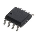
| 供应商器件封装 | 8-SOIC N |
| 其它名称 | TC7660SEOA713CT |
| 包装 | 剪切带 (CT) |
| 同步整流器 | 无 |
| 商标 | Microchip Technology |
| 安装类型 | 表面贴装 |
| 安装风格 | SMD/SMT |
| 宽度 | 3.91 mm |
| 封装 | Reel |
| 封装/外壳 | 8-SOIC(0.154",3.90mm 宽) |
| 封装/箱体 | SOIC-8 |
| 工作温度 | -40°C ~ 85°C |
| 工作温度范围 | - 40 C to + 85 C |
| 工厂包装数量 | 3300 |
| 开关频率 | 45 kHz |
| 最大工作温度 | + 85 C |
| 最大输入电压 | 12 V |
| 最小工作温度 | - 40 C |
| 最小输入电压 | 1.5 V |
| 标准包装 | 1 |
| 电压-输入 | 1.5 V ~ 12 V |
| 电压-输出 | -1.5 V ~ -12 V |
| 电流-输出 | 20mA |
| 电源电压-最小 | 1.5 V |
| 电源电流 | 300 uA |
| 类型 | Buck |
| 输入电压 | 5 V |
| 输出数 | 1 |
| 输出电压 | - 12 V |
| 输出电流 | 20 mA |
| 输出端数量 | 1 Output |
| 输出类型 | 可调式 |
| 频率-开关 | 10kHz ~ 45kHz |


- 商务部:美国ITC正式对集成电路等产品启动337调查
- 曝三星4nm工艺存在良率问题 高通将骁龙8 Gen1或转产台积电
- 太阳诱电将投资9.5亿元在常州建新厂生产MLCC 预计2023年完工
- 英特尔发布欧洲新工厂建设计划 深化IDM 2.0 战略
- 台积电先进制程称霸业界 有大客户加持明年业绩稳了
- 达到5530亿美元!SIA预计今年全球半导体销售额将创下新高
- 英特尔拟将自动驾驶子公司Mobileye上市 估值或超500亿美元
- 三星加码芯片和SET,合并消费电子和移动部门,撤换高东真等 CEO
- 三星电子宣布重大人事变动 还合并消费电子和移动部门
- 海关总署:前11个月进口集成电路产品价值2.52万亿元 增长14.8%


PDF Datasheet 数据手册内容提取
TC7660S Super Charge Pump DC-to-DC Voltage Converter Features Package Types • Oscillator boost from 10kHz to 45kHz PDIP/SOIC • Converts +5V Logic Supply to ±5V System • Wide Input Voltage Range: +1.5V to +12V BOOST 1 8 V+ • Efficient Voltage Conversion (99.9%, typical) CAP+ 2 7 OSC • Excellent Power Efficiency (98%, typical) TC7660S LOW GND 3 6 • Low Power Consumption: 80µA (typical) @ VIN = 5V VOLTAGE (LV) • Low Cost and Easy to Use CAP- 4 5 VOUT - Only Two External Capacitors Required • Available in 8-Pin Small Outline (SOIC) and 8-Pin PDIP Packages General Description • Improved ESD Protection (10kV HBM) The TC7660S device is a pin-compatible replacement • No External Diode Required for High-Voltage for the industry standard 7660 charge pump voltage Operation converter. It converts a +1.5V to +12V input to a corre- Applications sponding -1.5V to -12V output using only two low-cost capacitors, eliminating inductors and their associated • RS-232 Negative Power Supply cost, size and electromagnetic interference (EMI). • Simple Conversion of +5V to ±5V Supplies Added features include an extended supply range to • Voltage Multiplication V = ± n V+ 12V, and a frequency boost pin for higher operating fre- OUT quency, allowing the use of smaller external capacitors. • Negative Supplies for Data Acquisition Systems and Instrumentation The on-board oscillator operates at a nominal fre- quency of 10kHz. Frequency is increased to 45kHz when pin 1 is connected to V+. Operation below 10kHz (for lower supply current applications) is possible by connecting an external capacitor from OSC to ground (with pin 1 open). The TC7660S is available in 8-Pin PDIP and 8-Pin Small Outline (SOIC) packages in commercial and extended temperature ranges. 2001-2015 Microchip Technology Inc. DS20001467C-page 1
TC7660S Functional Block Diagram V+CAP+ 8 2 1 BOOST 7 RC Voltage 4 OSC Oscillator 2 Level CAP- Translator 6 LV 5 V OUT IInntteerrnnaall VVooltltaaggee RReegguulalatotror Logic Network TC7660S 3 GND DS20001467C-page 2 2001-2015 Microchip Technology Inc.
TC7660S 1.0 ELECTRICAL Notice†: Stresses above those listed under “Maximum CHARACTERISTICS Ratings” may cause permanent damage to the device. This is a stress rating only and functional operation of the device at those or any other conditions above those Absolute Maximum Ratings† indicated in the operational sections of this specification is not intended. Exposure to maximum Supply Voltage................................................................+13V rating conditions for extended periods may affect LV, Boost, and OSC Inputs Voltage: (Note1) ...................................-0.3V to (V+ + 0.3V) for V+ < 5.5V device reliability. .........................(V+ – 5.5V) to (V+ + 0.3V) for V+ > 5.5V Current into LV.........................................20µA for V+ > 3.5V Note1: Connecting any input terminal to Output Short Duration (VSUPPLY 5.5V)...............Continuous voltages greater than V+ or less than Package Power Dissipation: (TA +70°C) (Note2) GND may cause destructive latch-up. It 8-Pin PDIP..........................................................730mW is recommended that no inputs from 8-Pin SOIC..........................................................470mW sources operating from external Lead Temperature (Soldering, 10s)........................... +300°C supplies be applied prior to “power up” of the TC7660S. 2: Derate linearly above +50°C by 5.5mW/°C. ELECTRICAL SPECIFICATIONS Electrical Characteristics: Unless otherwise noted, specifications measured over operating temperature range with V+ = 5V, C = 0, refer to test circuit in Figure4-1. OSC Parameters Sym. Min. Typ. Max. Units Conditions Supply Current I+ — 80 160 µA R = L (Boost pin OPEN or GND) — — 180 0°C T +70°C A — — 180 -40°C T +85°C A — — 200 -55°C T +125°C A Supply Current I+ — — 300 µA 0°C T +70°C A (Boost pin = V+) — — 350 -40°C T +85°C A — — 400 -55°C T +125°C A Supply Voltage Range, V+ 3.0 — 12 V Min. T Max, R = 10k, LV Open H A L High Supply Voltage Range, Low V+ 1.5 — 3.5 V Min. T Max, R = 10k, LV to GND L A L Output Source Resistance R — 60 100 I = 20mA OUT OUT — 70 120 I = 20mA, 0°C T +70°C OUT A — 70 120 I = 20mA, -40°C T +85°C OUT A — 105 150 I = 20mA, -55°C T +125°C OUT A — — 250 V+ = 2V, I = 3mA, LV to GND OUT 0°C T +70°C A — — 400 V+ = 2V, I = 3mA, LV to GND OUT -55°C T +125°C A Oscillator Frequency f — 10 — kHz Pin 7 open, Pin 1 open or GND OSC 45 Boost Pin = V+ Power Efficiency P 96 98 — % R = 5kBoost Pin Open EFF L 95 98 — T T T ; Boost Pin Open MIN A MAX — 88 — Boost Pin = V+ 2001-2015 Microchip Technology Inc. DS20001467C-page 3
TC7660S ELECTRICAL SPECIFICATIONS (CONTINUED) Electrical Characteristics: Unless otherwise noted, specifications measured over operating temperature range with V+ = 5V, C = 0, refer to test circuit in Figure4-1. OSC Parameters Sym. Min. Typ. Max. Units Conditions Voltage Conversion V 99 99.9 — % R = OUTEFF L Efficiency Oscillator Impedance Z — 1 — M V+ = 2V OSC — 100 — k V+ = 5V TEMPERATURE SPECIFICATIONS Electrical Characteristics: Unless otherwise noted, specifications measured over operating temperature range with V+ = 5V, C = 0, refer to test circuit in Figure4-1. OSC Parameters Sym. Min. Typ. Max. Units Conditions Temperature Ranges Operating Temperature Range T 0 — +70 °C C suffix A T -40 — +85 °C E suffix A T -40 — +125 °C V suffix A Storage Temperature Range T -65 — +150 °C A Thermal Package Resistances Thermal Resistance, 8LD PDIP — 89.3 — °C/W JA Thermal Resistance, 8LD SOIC — 148.5 — °C/W JA DS20001467C-page 4 2001-2015 Microchip Technology Inc.
TC7660S 2.0 TYPICAL PERFORMANCE CURVES Note: The graphs and tables provided following this note are a statistical summary based on a limited number of samples and are provided for informational purposes only. The performance characteristics listed herein are not tested or guaranteed. In some graphs or tables, the data presented may be outside the specified operating range (e.g., outside specified power supply range) and therefore outside the warranted range. Note: Unless otherwise indicated, C = C = 10 µF, ESR = ESR = 1, T = 25°C. See Figure4-1. 1 2 C1 C2 A IN 12 60 Hz) 10 Hz) 50 k k Y ( Y ( NC 8 NC 40 UE UE VIN = 5V Q Q RE 6 VIN = 5V RE 30 R F R F VIN = 12V O 4 O 20 T T CILLA 2 VIN = 12V CILLA 10 S S O O 0 0 -40 -20 0 20 40 60 80 100 -40 -20 0 20 40 60 80 100 TEMPERATURE (°C) TEMPERATURE (°C) FIGURE 2-1: Unloaded Oscillator FIGURE 2-4: Unloaded Oscillator Frequency vs. Temperature. Frequency vs. Temperature with Boost Pin = V . IN 1000 %)101.0 Y ( C 800 EN100.5 CI FI Without Load 600 VIN = 12V N EF100.0 μA) SIO 99.5 I (DD400 NVER 10K Load O 99.0 C 200 E VIN = 5V AG 98.5 0-40 -20 0 20 40 60 80 100 VOLT 98.01 2 3 4 5 6 7 8 9 T1A0= 1215°C12 TEMPERATURE (°C) INPUT VOLTAGE VIN (V) FIGURE 2-2: Supply Current vs. FIGURE 2-5: Voltage Conversion. Temperature (with Boost Pin = V ). IN 100 100 Ω) Ω) OURCE RESISTANCE ( 357000 OURCE RESISTANCE ( 468000 VIN = 2.5V VIN = 5.5V OUTPUT S 10 IOUTTA == 2 205m°CA OUTPUT S 200 1.5 2.5 3.5 4.5 5.5 6.5 7.5 8.5 9.5 10.511.5 12 -40 -20 0 20 40 60 80 100 SUPPLY VOLTAGE (V) TEMPERATURE (°C) FIGURE 2-3: Output Source Resistance FIGURE 2-6: Output Source Resistance vs. Supply Voltage. vs. Temperature. 2001-2015 Microchip Technology Inc. DS20001467C-page 5
TC7660S Note: Unless otherwise indicated, C = C = 10 µF, ESR = ESR = 1, T = 25°C. See Figure4-1. 1 2 C1 C2 A 100 0 90 Boost Pin = Open (V)OUT --24 CY (%) 678000 Boost Pin = V+ V N VOLTAGE --68 R EFFICIE 345000 PUT OWE 20 UT -10 P 10 O 0 -12 050050 5000000 00 0 00 0 10 20 30 40 50 60 70 80 90 100 1.1.2.3.4.6. 7.9.0.5.0.5.0. 5.0. 0. 5.0. 11223 34 5 56 OUTPUT CURRENT (mA) LOAD CURRENT (mA) FIGURE 2-7: Output Voltage vs. Output FIGURE 2-10: Power Conversion Current. Efficiency vs. Load. 200 200 175 175 μRRENT I (A)DD111520050 VIN = 12.5V μRENT I (A)DD111520050 VIN = 12.5V U R LY C 75 Y CU 75 SUPP 5205 VIN = 5.5V SUPPL 5205 VIN = 5.5V 0 0 -40 -20 0 20 40 60 80 100 -40 -20 0 20 40 60 80 100 TEMPERATURE (°C) TEMPERATURE (°C) FIGURE 2-8: Supply Current vs. FIGURE 2-11: Supply Current vs. Temperature. Temperature. 200 175 μA) 150 (D T ID125 REN 100 VIN = 12.5V R CU 75 Y PL 50 UP VIN = 5.5V S 25 0 -40 -20 0 20 40 60 80 100 TEMPERATURE (°C) FIGURE 2-9: Supply Current vs. Temperature. DS20001467C-page 6 2001-2015 Microchip Technology Inc.
TC7660S 3.0 PIN DESCRIPTIONS The descriptions of the pins are listed in Table3-1. TABLE 3-1: PIN FUNCTION TABLE Pin No. Symbol Description 1 BOOST Switching Frequency boost pin 2 CAP+ Charge pump capacitor positive terminal 3 GND Ground terminal 4 CAP- Charge pump capacitor negative terminal 5 V Output voltage OUT 6 LV Low voltage pin. Connect to GND for V+ < 3.5V 7 OSC Oscillator control input. Bypass with an external capacitor to slow the oscillator. 8 V+ Power supply positive voltage input 3.1 Switching Frequency Boost Pin It is recommended that a low ESR capacitor be used. (Boost) Additionally, larger values will lower the output ripple. By connecting the boost pin (pin 1), the switching 3.6 Low Voltage Pin (LV) frequency of the charge pump is increased from 10kHz The low voltage pin ensures proper operation of the typical to 45kHz typical. By connecting the boost pin (pin1), to the V+ pin (pin 8), the switching frequency of internal oscillator for input voltages below 3.5V. The low voltage pin should be connected to ground (GND) for the charge pump is increased from 10kHz typical to input voltages below 3.5V. Otherwise, the low voltage 45kHz typical. pin should be allowed to float. 3.2 Charge Pump Capacitor (CAP+) 3.7 Oscillator Control Input (OSC) Positive connection for the charge pump capacitor, or The oscillator control input can be utilized to slow down flying capacitor, used to transfer charge from the input or speed up the operation of the TC7660S. Refer to source to the output. In the voltage-inverting Section5.4 “Changing the TC7660S Oscillator configuration, the charge pump capacitor is charged to Frequency”, for details on altering the oscillator the input voltage during the first half of the switching frequency. cycle. During the second half of the switching cycle, the charge pump capacitor is inverted and charge is 3.8 Power Supply (V+) transferred to the output capacitor and load. Positive power supply input voltage connection. It is It is recommended that a low ESR (equivalent series recommended that a low ESR capacitor be used to resistance) capacitor be used. Additionally, larger bypass the power supply input to ground (GND). values will lower the output resistance. 3.3 Ground (GND) Input and output zero volt reference. 3.4 Charge Pump Capacitor (CAP-) Negative connection for the charge pump capacitor, or flying capacitor, used to transfer charge from the input to the output. Proper orientation is imperative when using a polarized capacitor. 3.5 Output Voltage (V ) OUT Negative connection for the charge pump output capacitor. In the voltage-inverting configuration, the charge pump output capacitor supplies the output load during the first half of the switching cycle. During the second half of the switching cycle, charge is restored to the charge pump output capacitor. 2001-2015 Microchip Technology Inc. DS20001467C-page 7
TC7660S 4.0 DETAILED DESCRIPTION S S 1 2 V+ 4.1 Theory of Operation + C The TC7660S contains all the necessary circuitry to 1 implement a voltage inverter, with the exception of two external capacitors, which may be inexpensive 10µF + C polarized electrolytic capacitors. Operation is best GND 2 S S 3 4 understood by considering Figure4-2, which shows an V = -V OUT IN idealized voltage inverter. Capacitor C is charged to a 1 voltage V+ for the half cycle when switches S and S 1 3 are closed. (Note that switches S and S are open 2 4 during this half cycle.) During the second half cycle of operation, switches S and S are closed, with S and 2 4 1 S open, thereby shifting capacitor C negatively by V+ FIGURE 4-2: Ideal Charge Pump Inverter. 3 1 volts. Charge is then transferred from C1 negatively by To improve low-voltage operation, the “LV” pin should V+ volts. Charge is then transferred from C1 to C2, such be connected to GND, disabling the regulator. For that the voltage on C2 is exactly V+ assuming ideal supply voltages greater than 3.5V, the LV terminal must switches and no load on C2. be left open to ensure latch-up-proof operation and The four switches in Figure4-2 are MOS power prevent device damage. switches; S1 is a P-channel device, and S2, S3 and S4 4.2 Theoretical Power Efficiency are N-channel devices. The main difficulty with this Considerations approach is that in integrating the switches, the sub- strates of S and S must always remain In theory, a capacitive charge pump can approach 3 4 reverse-biased with respect to their sources, but not so 100% efficiency if certain conditions are met: much as to degrade their ON resistances. In addition, (1) The drive circuitry consumes minimal power. at circuit start-up, and under output short circuit condi- (2) The output switches have extremely low ON tions (VOUT = V+), the output voltage must be sensed resistance and virtually no offset. and the substrate bias adjusted accordingly. Failure to (3) The impedances of the pump and reservoir accomplish this will result in high power losses and capacitors are negligible at the pump frequency. probable device latch-up. The TC7660S approaches these conditions for nega- This problem is eliminated in the TC7660S by a logic tive voltage multiplication if large values of C and C 1 2 network which senses the output voltage (VOUT) are used. Energy is lost only in the transfer of charge together with the level translators, and switches the between capacitors if a change in voltage occurs. The substrates of S3 and S4 to the correct level to maintain energy lost is defined by: necessary reverse bias. E = 1/2 C (V 2 – V 2) 1 1 2 V and V are the voltages on C during the pump and V+ I tra1nsfer c2ycles. If the impedance1s of C and C are rel- S 1 2 1 8 atively high at the pump frequency (refer to Figure4-2) C1 + 23 TC7660S 76 COSCIL (+V5+V) cdoiffmerpeanrceed itno vthoelt avgaeluse V o1f aRnLd, tVhe2.r eT hweilrl ebfeo rae ,s iut biss tdaenstiiar-l 10µF able not only to make C as large as possible to 4 5 R 2 L eliminate output voltage ripple, but also to employ a correspondingly large value for C in order to achieve V 1 OUT maximum efficiency of operation. C 2 4.3 Dos and Don'ts + 10µF • Do not exceed maximum supply voltages. Note: For large values of C (>1000pF), the • Do not connect the LV terminal to GND for supply OSC values of C1 and C2 should be increased to voltages greater than 3.5V. 100F. • Do not short circuit the output to V+ supply for voltages above 5.5V for extended periods; how- FIGURE 4-1: TC7660S Test Circuit. ever, transient conditions including start-up are The voltage regulator portion of the TC7660S is an okay. integral part of the anti-latch-up circuitry. Its inherent • When using polarized capacitors in the inverting voltage drop can, however, degrade operation at low mode, the + terminal of C must be connected to 1 voltages. pin 2 of the TC7660S and the + terminal of C 2 must be connected to GND. DS20001467C-page 8 2001-2015 Microchip Technology Inc.
TC7660S 5.0 APPLICATIONS INFORMATION The dynamic output impedance of the TC7660S is due, primarily, to capacitive reactance of the charge transfer 5.1 Simple Negative Voltage capacitor (C1). Since this capacitor is connected to the Converter output for only half of the cycle, the equation is: Figure5-1 shows typical connections to provide a EQUATION negative supply where a positive supply is available. A similar scheme may be employed for supply voltages X = -----2------ = 3.18 anywhere in the operating range of +1.5V to +12V, C 2fC1 where: keeping in mind that pin 6 (LV) is tied to the supply f = 10kHz and C1 = 10µF. negative (GND) only for supply voltages below 3.5V. 5.2 Paralleling Devices V+ 1 8 Any number of TC7660S voltage converters may be paralleled to reduce output resistance (Figure5-2). The 2 7 V * C1 + 3 TC7660S 6 C2 OUT dreesveicrveo rier qcuaipreasc iittosr ,o Cw2n, psuemrvpe sc aaplla dceitvoirc, eCs, . wThhiele reeasuchl- 10µF + 10µF 1 tant output resistance would be approximately: 4 5 EQUATION * V = -V+ for 1.5V V+ 12V OUT R of TC7660S OUT R = --------------------------------------------------- FIGURE 5-1: Simple Negative Converter. OUT nnumber of devices The output characteristics of the circuit in Figure5-1 are those of a nearly ideal voltage source in series with a 70resistor. Thus, for a load current of -10mA and a supply voltage of +5V, the output voltage would be -4.3V. V+ 1 8 2 7 1 8 + TC7660S C1 3 6 2 7 RL + TC7660S 4 “1” 5 C1 3 6 4 “n” 5 C 2 + FIGURE 5-2: Paralleling Devices Lowers Output Impedance. V+ 1 8 2 7 1 8 + TC7660S 10µF 3 6 2 7 + TC7660S 4 “1” 5 10µF 3 6 4 “n” 5 VOUT * 10µF + 10µF + * V = -n V+ for 1.5V V+ 12V OUT FIGURE 5-3: Increased Output Voltage By Cascading Devices. 2001-2015 Microchip Technology Inc. DS20001467C-page 9
TC7660S 5.3 Cascading Devices The TC7660S may be cascaded as shown (Figure5-3) to produce larger negative multiplication of the initial 1 8 V+ supply voltage. However, due to the finite efficiency of 2 7 each device, the practical limit is 10 devices for light + TC7660S loads. The output voltage is defined by: C1 3 6 COSC EQUATION 4 5 VOUT C + 2 VOUT = –nV + where n is an integer representing the number of devices cascaded. The resulting output resistance would be approximately the weighted sum of the FIGURE 5-5: Lowering Oscillator individual TC7660S R values. Frequency. OUT 5.4 Changing the TC7660S Oscillator 5.5 Positive Voltage Multiplication Frequency The TC7660S may be employed to achieve positive It may be desirable in some applications (due to noise voltage multiplication using the circuit shown in or other considerations) to increase the oscillator fre- Figure5-6. In this application, the pump inverter quency. Pin 1, frequency boost pin, may be connected to V+ to increase oscillator frequency to 45kHz from a switches of the TC7660S are used to charge C1 to a voltage level of V+–V (where V+ is the supply voltage nominal of 10kHz for an input supply voltage of 5.0V. F and V is the forward voltage drop of diode D ). On the The oscillator may also be synchronized to an external F 1 transfer cycle, the voltage on C plus the supply voltage clock as shown in Figure5-4. In order to prevent possi- 1 (V+) is applied through diode D to capacitor C . The ble device latch-up, a 1kΩ resistor must be used in 2 2 voltage thus created on C becomes (2V+) – (2V ), or series with the clock output. In a situation where the 2 F twice the supply voltage minus the combined forward designer has generated the external clock frequency voltage drops of diodes D and D using TTL logic, the addition of a 10kΩ pull-up resistor 1 2. to V+ supply is required. Note that the pump frequency The source impedance of the output (V ) will depend OUT with external clocking, as with internal clocking, will be on the output current, but for V+ = 5V and an output half of the clock frequency. Output transitions occur on current of 10mA, it will be approximately 60Ω. the positive-going edge of the clock. V+ V+ V+ 1 8 1 8 1k CMOS 10µF + 23 TC7660S 76 GATE 23 TC7660S 76 D1 D2 V(2O VU+T) = - (2 VF) 4 “1” 5 VOUT 4 5 + + C C 1 2 10µF + FIGURE 5-6: Positive Voltage Multiplier. FIGURE 5-4: External Clocking. It is also possible to increase the conversion efficiency of the TC7660S at low load levels by lowering the oscillator frequency. This reduces the switching losses, and is achieved by connecting an additional capacitor, C , as shown in Figure5-5. Lowering the oscillator OSC frequency will cause an undesirable increase in the impedance of the pump (C ) and the reservoir (C ) 1 2 capacitors. To overcome this, increase the values of C 1 and C by the same factor that the frequency has been 2 reduced. For example, the addition of a 100pF capacitor between pin 7 (OSC) and pin 8 (V+) will lower the oscillator frequency to 1kHz from its nominal frequency of 10kHz (a multiple of 10), and necessitate a corresponding increase in the values of C and C 1 2 (from 10µF to 100µF). DS20001467C-page 10 2001-2015 Microchip Technology Inc.
TC7660S 5.6 Combined Negative Voltage Conversion and Positive Supply VOUT = -V- Multiplication 1 8 + Figure5-7 combines the functions shown in Figure5-3 2 7 10µF and Figure5-6 to provide negative voltage conversion C1 + TC7660S 1M and positive voltage multiplication simultaneously. For 10µF 3 6 example, this approach would be suitable for generat- 4 5 ing +9V and -5V from an existing +5V supply. In this instance, capacitors C and C perform the pump and V- input 1 3 reservoir functions, respectively, for the generation of FIGURE 5-8: Positive Voltage the negative voltage, while capacitors C and C are 2 4 Conversion. pump and reservoir, respectively, for the multiplied pos- itive voltage. There is a penalty in this configuration which combines both functions, however, in that the 5.8 Voltage Splitting source impedances of the generated supplies will be The same bidirectional characteristics used in somewhat higher due to the finite impedance of the Figure5-8 can also be used to split a higher supply in common charge pump driver at pin 2 of the device. half, as shown in Figure5-9. The combined load will be evenly shared between the two sides. Once again, a V+ high value resistor to the LV pin ensures start-up. Because the switches share the load in parallel, the V OUT 1 8 = -V+ output impedance is much lower than in the standard 2 7 + C3 circuits, and higher currents can be drawn from the TC7660S D device. By using this circuit, and then the circuit of 3 6 1 Figure5-3, +15V can be converted (via +7.5V and -7.5V) +C1 4 + 5 D2 V(2O VU+T) = - (2 VF) troe sias tannocme in(~a2l 5-01Ω5V)., though with rather high series C + 2 C4 V+ + RL1 50μF 1 8 FIGURE 5-7: Combined Negative Converter and Positive Multiplier. VVO+U–TV =– 50μF + 100 kΩ 23 TC7660S 76 1 MΩ 2 – 5.7 Efficient Positive Voltage 4 5 Multiplication/Conversion RL2 Since the switches that allow the charge pumping 50μF + – operation are bidirectional, the charge transfer can be V– performed backwards as easily as forwards. Figure5-8 shows a TC7660S transforming -5V to +5V (or +5V to +10V, etc.). The only problem is that the FIGURE 5-9: Splitting a Supply in Half. internal clock and switch-drive section will not operate until some positive voltage has been generated. An ini- 5.9 Negative Voltage Generation for tial inefficient pump, as shown in Figure5-7, could be Display ADCs used to start this circuit up, after which it will bypass the other (D and D in Figure5-7 would never turn on), or The TC7106 is designed to work from a 9V battery. 1 2 else the diode and resistor shown dotted in Figure5-8 With a fixed power supply system, the TC7106 will can be used to “force” the internal regulator on. perform conversions with input signal referenced to power supply ground. 5.10 Negative Supply Generation for 4½ Digit Data Acquisition System The TC7135 is a 4½ digit ADC operating from ±5V supplies. The TC7660S provides an inexpensive -5V source. (See AN16 and AN17 for TC7135 interface details and software routines.) 2001-2015 Microchip Technology Inc. DS20001467C-page 11
TC7660S 6.0 PACKAGING INFORMATION 6.1 Package Marking Information 8-Lead PDIP (300 mil) Example Example XXXXXXXX TC7660S TC7660S XXXXXNNN CPA e 3 256 EPA e 3 256 YYWW 1545 1545 8-Lead SOIC (3.90 mm) Example TC7660SE OA 1545 e3 NNN 256 Legend: XX...X Customer-specific information Y Year code (last digit of calendar year) YY Year code (last 2 digits of calendar year) WW Week code (week of January 1 is week ‘01’) NNN Alphanumeric traceability code e3 Pb-free JEDEC designator for Matte Tin (Sn) * This package is Pb-free. The Pb-free JEDEC designator ( e 3 ) can be found on the outer packaging for this package. Note: In the event the full Microchip part number cannot be marked on one line, it will be carried over to the next line thus limiting the number of available characters for customer specific information. DS20001467C-page 12 2001-2015 Microchip Technology Inc.
TC7660S (cid:27)(cid:16)(cid:47)(cid:72)(cid:68)(cid:71)(cid:3)(cid:51)(cid:79)(cid:68)(cid:86)(cid:87)(cid:76)(cid:70)(cid:3)(cid:39)(cid:88)(cid:68)(cid:79)(cid:3)(cid:44)(cid:81)(cid:16)(cid:47)(cid:76)(cid:81)(cid:72)(cid:3)(cid:11)(cid:51)(cid:36)(cid:12)(cid:3)(cid:16)(cid:3)(cid:22)(cid:19)(cid:19)(cid:3)(cid:80)(cid:76)(cid:79)(cid:3)(cid:37)(cid:82)(cid:71)(cid:92)(cid:3)(cid:62)(cid:51)(cid:39)(cid:44)(cid:51)(cid:64) (cid:49)(cid:82)(cid:87)(cid:72)(cid:29) For the most current package drawings, please see the Microchip Packaging Specification located at http://www.microchip.com/packaging D A N B E1 NOTE 1 1 2 TOP VIEW E C A A2 (cid:51)(cid:47)(cid:36)(cid:49)(cid:40) L c A1 e eB 8X b1 8X b .010 C SIDE VIEW END VIEW Microchip Technology Drawing No. C04-018D Sheet 1 of 2 2001-2015 Microchip Technology Inc. DS20001467C-page 13
TC7660S (cid:27)(cid:16)(cid:47)(cid:72)(cid:68)(cid:71)(cid:3)(cid:51)(cid:79)(cid:68)(cid:86)(cid:87)(cid:76)(cid:70)(cid:3)(cid:39)(cid:88)(cid:68)(cid:79)(cid:3)(cid:44)(cid:81)(cid:16)(cid:47)(cid:76)(cid:81)(cid:72)(cid:3)(cid:11)(cid:51)(cid:36)(cid:12)(cid:3)(cid:16)(cid:3)(cid:22)(cid:19)(cid:19)(cid:3)(cid:80)(cid:76)(cid:79)(cid:3)(cid:37)(cid:82)(cid:71)(cid:92)(cid:3)(cid:62)(cid:51)(cid:39)(cid:44)(cid:51)(cid:64) (cid:49)(cid:82)(cid:87)(cid:72)(cid:29) For the most current package drawings, please see the Microchip Packaging Specification located at http://www.microchip.com/packaging ALTERNATE LEAD DESIGN (VENDOR DEPENDENT) DATUM A DATUM A b b e e 2 2 e e Units INCHES Dimension Limits MIN NOM MAX Number of Pins N 8 Pitch e .100 BSC Top to Seating Plane A - - .210 Molded Package Thickness A2 .115 .130 .195 Base to Seating Plane A1 .015 - - Shoulder to Shoulder Width E .290 .310 .325 Molded Package Width E1 .240 .250 .280 Overall Length D .348 .365 .400 Tip to Seating Plane L .115 .130 .150 Lead Thickness c .008 .010 .015 Upper Lead Width b1 .040 .060 .070 Lower Lead Width b .014 .018 .022 Overall Row Spacing § eB - - .430 Notes: 1. Pin 1 visual index feature may vary, but must be located within the hatched area. 2. § Significant Characteristic 3. Dimensions D and E1 do not include mold flash or protrusions. Mold flash or protrusions shall not exceed .010" per side. 4. Dimensioning and tolerancing per ASME Y14.5M BSC: Basic Dimension. Theoretically exact value shown without tolerances. Microchip Technology Drawing No. C04-018D Sheet 2 of 2 DS20001467C-page 14 2001-2015 Microchip Technology Inc.
TC7660S Note: For the most current package drawings, please see the Microchip Packaging Specification located at http://www.microchip.com/packaging 2001-2015 Microchip Technology Inc. DS20001467C-page 15
TC7660S Note: For the most current package drawings, please see the Microchip Packaging Specification located at http://www.microchip.com/packaging DS20001467C-page 16 2001-2015 Microchip Technology Inc.
TC7660S (cid:2)(cid:3)(cid:4)(cid:5)(cid:6)(cid:7)(cid:8)(cid:9)(cid:10)(cid:6)(cid:11)(cid:12)(cid:13)(cid:14)(cid:8)(cid:15)(cid:16)(cid:6)(cid:10)(cid:10)(cid:8)(cid:17)(cid:18)(cid:12)(cid:10)(cid:13)(cid:19)(cid:5)(cid:8)(cid:20)(cid:17)(cid:21)(cid:22)(cid:8)(cid:23)(cid:8)(cid:24)(cid:6)(cid:25)(cid:25)(cid:26)(cid:27)(cid:28)(cid:8)(cid:29)(cid:30)(cid:31) (cid:8)(cid:16)(cid:16)(cid:8)!(cid:26)(cid:7)"(cid:8)#(cid:15)(cid:17)$%& (cid:24)(cid:26)(cid:12)(cid:5)’ (cid:30)(cid:10)(cid:9)(cid:2)(cid:31)(cid:11)(cid:14)(cid:2)!(cid:10)"(cid:31)(cid:2)(cid:8)#(cid:9)(cid:9)(cid:14)(cid:15)(cid:31)(cid:2)(cid:12)(cid:28)(cid:8)$(cid:28)(cid:17)(cid:14)(cid:2)%(cid:9)(cid:28)&(cid:7)(cid:15)(cid:17)"’(cid:2)(cid:12)(cid:16)(cid:14)(cid:28)"(cid:14)(cid:2)"(cid:14)(cid:14)(cid:2)(cid:31)(cid:11)(cid:14)(cid:2)(cid:6)(cid:7)(cid:8)(cid:9)(cid:10)(cid:8)(cid:11)(cid:7)(cid:12)(cid:2)((cid:28)(cid:8)$(cid:28)(cid:17)(cid:7)(cid:15)(cid:17)(cid:2)(cid:22)(cid:12)(cid:14)(cid:8)(cid:7))(cid:7)(cid:8)(cid:28)(cid:31)(cid:7)(cid:10)(cid:15)(cid:2)(cid:16)(cid:10)(cid:8)(cid:28)(cid:31)(cid:14)%(cid:2)(cid:28)(cid:31)(cid:2) (cid:11)(cid:31)(cid:31)(cid:12)*++&&&(cid:20)!(cid:7)(cid:8)(cid:9)(cid:10)(cid:8)(cid:11)(cid:7)(cid:12)(cid:20)(cid:8)(cid:10)!+(cid:12)(cid:28)(cid:8)$(cid:28)(cid:17)(cid:7)(cid:15)(cid:17) 2001-2015 Microchip Technology Inc. DS20001467C-page 17
TC7660S NOTES: DS20001467C-page 18 2001-2015 Microchip Technology Inc.
TC7660S APPENDIX A: REVISION HISTORY Revision C (November 2015) The following is the list of modifications. 1. Updated Section1.0 “Electrical Characteris- tics”. 2. Added Temperature Specifications table. 3. Updated Product Identification System section. 4. Minor typographical errors. Revision B (August 2013) The following is the list of modifications. 1. Added Appendix A and the “Product Identifi- cation System” page. 2. Updated Section6.0 “Packaging Information”. Revision A (May 2001) • Original release of this document. 2001-2015 Microchip Technology Inc. DS20001467C-page 19
TC7660S NOTES: DS20001467C-page 20 2001-2015 Microchip Technology Inc.
TC7660S PRODUCT IDENTIFICATION SYSTEM To order or obtain information, e.g., on pricing or delivery, refer to the factory or the listed sales office. PART NO. X /XX [X](1) Examples: a) TC7660SCPA: Commercial temperature, Device Temperature Package Tape and Reel PDIP package Range Option a) TC7660SCPA: Commercial temperature, PDIP package a) TC7660SEPA: Extended temperature, PDIP Device: TC7660S: DC-to-DC Voltage Converter package b) TC7660SCOA: Commercial temperature, SOIC package Temperature C = 0°C to +70°C (Commercial) c) TC7660SCOA713: Tape and Reel, Range: E = -40°C to +85°C (Extended) Commercial temperature, SOIC package V = -40°C to +125°C (Various) d) TC7660SEOA: Extended temperature, SOIC package Package: PA = 8-Lead Plastic Dual In-Line - 300mil Body (PDIP) e) TC7660SEOA713: Tape and Reel, Extended OA = 8-Lead Plastic Small Outline - Narrow, 3.90mm Body (SOIC) temperature, SOIC package f) TC7660SEOA723: Reverse Tape and Reel, Tape and Blank = Tube Extended temperature, SOIC package Reel 713 = Tape and Reel (SOIC only) 723 = Reverse Tape and Reel (SOIC only) Note1: Tape and Reel identifier only appears in the catalog part number description. This identifier is used for ordering purposes and is not printed on the device package. Check with your Microchip Sales Office for package availability with the Tape and Reel option. 2001-2015 Microchip Technology Inc. DS20001467C-page 21
TC7660S NOTES: DS20001467C-page 22 2001-2015 Microchip Technology Inc.
Note the following details of the code protection feature on Microchip devices: • Microchip products meet the specification contained in their particular Microchip Data Sheet. • Microchip believes that its family of products is one of the most secure families of its kind on the market today, when used in the intended manner and under normal conditions. • There are dishonest and possibly illegal methods used to breach the code protection feature. All of these methods, to our knowledge, require using the Microchip products in a manner outside the operating specifications contained in Microchip’s Data Sheets. Most likely, the person doing so is engaged in theft of intellectual property. • Microchip is willing to work with the customer who is concerned about the integrity of their code. • Neither Microchip nor any other semiconductor manufacturer can guarantee the security of their code. Code protection does not mean that we are guaranteeing the product as “unbreakable.” Code protection is constantly evolving. We at Microchip are committed to continuously improving the code protection features of our products. Attempts to break Microchip’s code protection feature may be a violation of the Digital Millennium Copyright Act. If such acts allow unauthorized access to your software or other copyrighted work, you may have a right to sue for relief under that Act. Information contained in this publication regarding device Trademarks applications and the like is provided only for your convenience The Microchip name and logo, the Microchip logo, dsPIC, and may be superseded by updates. It is your responsibility to FlashFlex, flexPWR, JukeBlox, KEELOQ, KEELOQ logo, Kleer, ensure that your application meets with your specifications. LANCheck, MediaLB, MOST, MOST logo, MPLAB, MICROCHIP MAKES NO REPRESENTATIONS OR OptoLyzer, PIC, PICSTART, PIC32 logo, RightTouch, SpyNIC, WARRANTIES OF ANY KIND WHETHER EXPRESS OR SST, SST Logo, SuperFlash and UNI/O are registered IMPLIED, WRITTEN OR ORAL, STATUTORY OR trademarks of Microchip Technology Incorporated in the OTHERWISE, RELATED TO THE INFORMATION, U.S.A. and other countries. INCLUDING BUT NOT LIMITED TO ITS CONDITION, QUALITY, PERFORMANCE, MERCHANTABILITY OR The Embedded Control Solutions Company and mTouch are FITNESS FOR PURPOSE. Microchip disclaims all liability registered trademarks of Microchip Technology Incorporated arising from this information and its use. Use of Microchip in the U.S.A. devices in life support and/or safety applications is entirely at Analog-for-the-Digital Age, BodyCom, chipKIT, chipKIT logo, the buyer’s risk, and the buyer agrees to defend, indemnify and CodeGuard, dsPICDEM, dsPICDEM.net, ECAN, In-Circuit hold harmless Microchip from any and all damages, claims, Serial Programming, ICSP, Inter-Chip Connectivity, KleerNet, suits, or expenses resulting from such use. No licenses are KleerNet logo, MiWi, motorBench, MPASM, MPF, MPLAB conveyed, implicitly or otherwise, under any Microchip Certified logo, MPLIB, MPLINK, MultiTRAK, NetDetach, intellectual property rights unless otherwise stated. Omniscient Code Generation, PICDEM, PICDEM.net, PICkit, PICtail, RightTouch logo, REAL ICE, SQI, Serial Quad I/O, Total Endurance, TSHARC, USBCheck, VariSense, ViewSpan, WiperLock, Wireless DNA, and ZENA are trademarks of Microchip Technology Incorporated in the U.S.A. and other countries. SQTP is a service mark of Microchip Technology Incorporated in the U.S.A. Silicon Storage Technology is a registered trademark of Microchip Technology Inc. in other countries. GestIC is a registered trademark of Microchip Technology Germany II GmbH & Co. KG, a subsidiary of Microchip Technology Inc., in other countries. All other trademarks mentioned herein are property of their respective companies. © 2001-2015, Microchip Technology Incorporated, Printed in the U.S.A., All Rights Reserved. ISBN: 978-1-5224-0013-4 QUALITY MANAGEMENT SYSTEM Microchip received ISO/TS-16949:2009 certification for its worldwide headquarters, design and wafer fabrication facilities in Chandler and CERTIFIED BY DNV Tempe, Arizona; Gresham, Oregon and design centers in California and India. The Company’s quality system processes and procedures == ISO/TS 16949 == are for its PIC® MCUs and dsPIC® DSCs, KEELOQ® code hopping devices, Serial EEPROMs, microperipherals, nonvolatile memory and analog products. In addition, Microchip’s quality system for the design and manufacture of development systems is ISO 9001:2000 certified. 2001-2015 Microchip Technology Inc. DS20001467C-page 23
Worldwide Sales and Service AMERICAS ASIA/PACIFIC ASIA/PACIFIC EUROPE Corporate Office Asia Pacific Office China - Xiamen Austria - Wels 2355 West Chandler Blvd. Suites 3707-14, 37th Floor Tel: 86-592-2388138 Tel: 43-7242-2244-39 Chandler, AZ 85224-6199 Tower 6, The Gateway Fax: 86-592-2388130 Fax: 43-7242-2244-393 Tel: 480-792-7200 Harbour City, Kowloon China - Zhuhai Denmark - Copenhagen Fax: 480-792-7277 Hong Kong Tel: 86-756-3210040 Tel: 45-4450-2828 Technical Support: Tel: 852-2943-5100 Fax: 86-756-3210049 Fax: 45-4485-2829 http://www.microchip.com/ Fax: 852-2401-3431 India - Bangalore France - Paris support Australia - Sydney Tel: 91-80-3090-4444 Tel: 33-1-69-53-63-20 Web Address: Tel: 61-2-9868-6733 Fax: 91-80-3090-4123 Fax: 33-1-69-30-90-79 www.microchip.com Fax: 61-2-9868-6755 India - New Delhi Germany - Dusseldorf Atlanta China - Beijing Tel: 91-11-4160-8631 Tel: 49-2129-3766400 Duluth, GA Tel: 678-957-9614 Tel: 86-10-8569-7000 Fax: 91-11-4160-8632 Germany - Karlsruhe Fax: 678-957-1455 Fax: 86-10-8528-2104 India - Pune Tel: 49-721-625370 China - Chengdu Tel: 91-20-3019-1500 Germany - Munich Austin, TX Tel: 512-257-3370 Tel: 86-28-8665-5511 Japan - Osaka Tel: 49-89-627-144-0 Fax: 86-28-8665-7889 Tel: 81-6-6152-7160 Fax: 49-89-627-144-44 Boston Westborough, MA China - Chongqing Fax: 81-6-6152-9310 Italy - Milan Tel: 774-760-0087 Tel: 86-23-8980-9588 Japan - Tokyo Tel: 39-0331-742611 Fax: 86-23-8980-9500 Tel: 81-3-6880- 3770 Fax: 39-0331-466781 Fax: 774-760-0088 China - Dongguan Fax: 81-3-6880-3771 Italy - Venice Chicago Itasca, IL Tel: 86-769-8702-9880 Korea - Daegu Tel: 39-049-7625286 Tel: 630-285-0071 China - Hangzhou Tel: 82-53-744-4301 Netherlands - Drunen Fax: 630-285-0075 Tel: 86-571-8792-8115 Fax: 82-53-744-4302 Tel: 31-416-690399 Fax: 86-571-8792-8116 Korea - Seoul Fax: 31-416-690340 Cleveland Independence, OH China - Hong Kong SAR Tel: 82-2-554-7200 Poland - Warsaw Tel: 216-447-0464 Tel: 852-2943-5100 Fax: 82-2-558-5932 or Tel: 48-22-3325737 Fax: 852-2401-3431 82-2-558-5934 Fax: 216-447-0643 Spain - Madrid Dallas China - Nanjing Malaysia - Kuala Lumpur Tel: 34-91-708-08-90 Addison, TX Tel: 86-25-8473-2460 Tel: 60-3-6201-9857 Fax: 34-91-708-08-91 Fax: 86-25-8473-2470 Fax: 60-3-6201-9859 Tel: 972-818-7423 Sweden - Stockholm Fax: 972-818-2924 China - Qingdao Malaysia - Penang Tel: 46-8-5090-4654 Tel: 86-532-8502-7355 Tel: 60-4-227-8870 Detroit UK - Wokingham Fax: 86-532-8502-7205 Fax: 60-4-227-4068 Novi, MI Tel: 44-118-921-5800 Tel: 248-848-4000 China - Shanghai Philippines - Manila Fax: 44-118-921-5820 Tel: 86-21-5407-5533 Tel: 63-2-634-9065 Houston, TX Fax: 86-21-5407-5066 Fax: 63-2-634-9069 Tel: 281-894-5983 China - Shenyang Singapore Indianapolis Tel: 86-24-2334-2829 Tel: 65-6334-8870 Noblesville, IN Fax: 86-24-2334-2393 Fax: 65-6334-8850 Tel: 317-773-8323 Fax: 317-773-5453 China - Shenzhen Taiwan - Hsin Chu Tel: 86-755-8864-2200 Tel: 886-3-5778-366 Los Angeles Fax: 86-755-8203-1760 Fax: 886-3-5770-955 Mission Viejo, CA Tel: 949-462-9523 China - Wuhan Taiwan - Kaohsiung Fax: 949-462-9608 Tel: 86-27-5980-5300 Tel: 886-7-213-7828 New York, NY Fax: 86-27-5980-5118 Taiwan - Taipei Tel: 631-435-6000 China - Xian Tel: 886-2-2508-8600 Tel: 86-29-8833-7252 Fax: 886-2-2508-0102 San Jose, CA Tel: 408-735-9110 Fax: 86-29-8833-7256 Thailand - Bangkok Tel: 66-2-694-1351 Canada - Toronto Fax: 66-2-694-1350 Tel: 905-673-0699 Fax: 905-673-6509 07/14/15 DS20001467C-page 24 2001-2015 Microchip Technology Inc.