ICGOO在线商城 > 集成电路(IC) > PMIC - 稳压器 - 线性 + 切换式 > TPS61130PW
 Datasheet下载
- 型号: TPS61130PW
- 制造商: Texas Instruments
- 库位|库存: xxxx|xxxx
- 要求:
| 数量阶梯 | 香港交货 | 国内含税 |
| +xxxx | $xxxx | ¥xxxx |
查看当月历史价格
查看今年历史价格
TPS61130PW产品简介:
ICGOO电子元器件商城为您提供TPS61130PW由Texas Instruments设计生产,在icgoo商城现货销售,并且可以通过原厂、代理商等渠道进行代购。 TPS61130PW价格参考¥13.03-¥26.70。Texas InstrumentsTPS61130PW封装/规格:PMIC - 稳压器 - 线性 + 切换式, Linear And Switching Voltage Regulator IC 2 Output Step-Down/Step-Up (Buck/Boost) (1), Linear (LDO) (1) 500kHz 16-TSSOP。您可以下载TPS61130PW参考资料、Datasheet数据手册功能说明书,资料中有TPS61130PW 详细功能的应用电路图电压和使用方法及教程。
TPS61130PW是德州仪器(Texas Instruments)推出的一款PMIC(电源管理集成电路),结合了线性稳压器和开关稳压器的功能。该器件主要用于便携式设备和低功耗应用,能够提供高效、稳定的电源管理解决方案。

 应用场景

1. 便携式电子产品:
   - 智能手机和平板电脑:TPS61130PW可以用于这些设备的电源管理系统中,确保电池供电时的高效转换和稳定输出电压。它能够在不同负载条件下保持高效率,延长电池寿命。
   - 可穿戴设备:如智能手表、健身追踪器等,对电源管理要求较高,TPS61130PW能够提供小尺寸、高效能的电源解决方案,适合空间受限的应用。

2. 物联网(IoT)设备:
   - 传感器节点:在物联网系统中,传感器节点通常需要长时间工作且功耗极低。TPS61130PW可以通过其高效的电源转换能力,确保传感器节点在低功耗模式下依然能稳定运行。
   - 无线通信模块:例如蓝牙、Wi-Fi模块等,TPS61130PW可以为其提供稳定的电源,同时减少发热,提高系统的可靠性和性能。

3. 医疗设备:
   - 便携式医疗仪器:如血糖仪、心率监测仪等,这些设备需要可靠的电源管理以确保测量结果的准确性。TPS61130PW的高效能和稳定性使其成为理想选择。
   - 植入式医疗设备:虽然植入式设备对电源管理有更高的安全性和可靠性要求,但TPS61130PW的小尺寸和高效能特性也使其适用于一些非关键部分的电源管理。

4. 工业自动化:
   - 远程监控系统:在工业环境中,远程监控系统需要长时间稳定运行,TPS61130PW可以通过其高效的电源管理能力,确保系统在各种环境条件下的正常工作。
   - 传感器网络:工业传感器网络中的节点设备同样需要高效的电源管理,TPS61130PW可以满足这些需求,确保数据采集的准确性和实时性。

总之,TPS61130PW凭借其高效、稳定、低功耗的特点,广泛应用于各类便携式电子设备、物联网设备、医疗设备以及工业自动化领域,为用户提供可靠的电源管理解决方案。
| 参数 | 数值 |
| 产品目录 | 集成电路 (IC)半导体 |
| 描述 | IC REG DL BCK/BST/LINEAR 16TSSOP稳压器—开关式稳压器 Adj 90% Eff SEPIC Converter |
| DevelopmentKit | TPS61130EVM-206 |
| 产品分类 | |
| 品牌 | Texas Instruments |
| 产品手册 | |
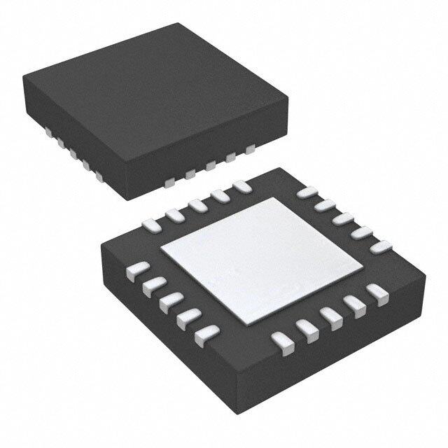
| 产品图片 |
|
| rohs | 符合RoHS无铅 / 符合限制有害物质指令(RoHS)规范要求 |
| 产品系列 | 电源管理 IC,稳压器—开关式稳压器,Texas Instruments TPS61130PW- |
| 数据手册 | |
| 产品型号 | TPS61130PW |
| 产品目录页面 | |
| 产品种类 | 稳压器—开关式稳压器 |
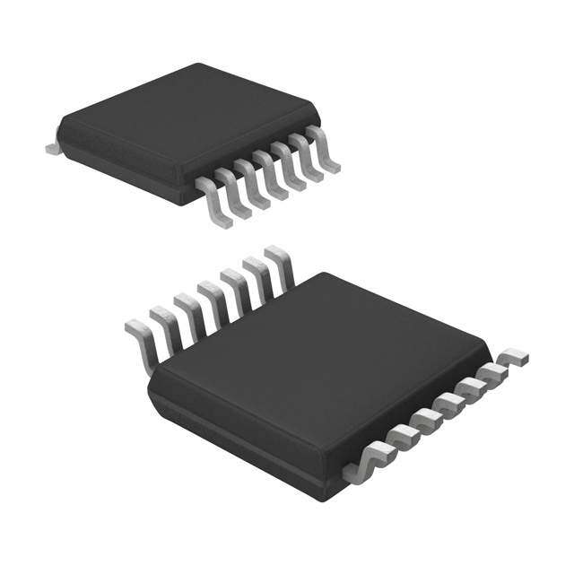
| 供应商器件封装 | 16-TSSOP |
| 其它名称 | 296-13521-5 |
| 功能 | 任何功能 |
| 包装 | 管件 |
| 单位重量 | 63 mg |
| 商标 | Texas Instruments |
| 安装类型 | 表面贴装 |
| 安装风格 | SMD/SMT |
| 封装 | Tube |
| 封装/外壳 | 16-TSSOP(0.173",4.40mm 宽) |
| 封装/箱体 | TSSOP-16 |
| 工作温度 | -40°C ~ 85°C |
| 工作温度范围 | - 40 C to + 85 C |
| 工厂包装数量 | 90 |
| 带LED驱动器 | 无 |
| 带定序器 | 无 |
| 带监控器 | 无 |
| 开关频率 | 500 kHz |
| 拓扑 | 降压/升压(1),线性(LDO)(1) |
| 拓扑结构 | Boost, Buck |
| 最大工作温度 | + 85 C |
| 最大输入电压 | 5.5 V |
| 最小工作温度 | - 40 C |
| 标准包装 | 90 |
| 电压-电源 | 1.8 V ~ 5.5 V |
| 电压/电流-输出1 | 2.5 V ~ 5.5 V,300mA |
| 电压/电流-输出2 | 2.5 V ~ 5.5 V,320mA |
| 电压/电流-输出3 | - |
| 类型 | DC/DC Converter |
| 系列 | TPS61130 |
| 输出数 | 2 |
| 输出电压 | 900 mV to 5.5 V |
| 输出电流 | 320 mA |
| 输出端数量 | 2 Output |
| 配用 | /product-detail/zh/TPS61130EVM-206/296-18974-ND/863796 |
| 频率-开关 | 500kHz |


- 商务部:美国ITC正式对集成电路等产品启动337调查
- 曝三星4nm工艺存在良率问题 高通将骁龙8 Gen1或转产台积电
- 太阳诱电将投资9.5亿元在常州建新厂生产MLCC 预计2023年完工
- 英特尔发布欧洲新工厂建设计划 深化IDM 2.0 战略
- 台积电先进制程称霸业界 有大客户加持明年业绩稳了
- 达到5530亿美元!SIA预计今年全球半导体销售额将创下新高
- 英特尔拟将自动驾驶子公司Mobileye上市 估值或超500亿美元
- 三星加码芯片和SET,合并消费电子和移动部门,撤换高东真等 CEO
- 三星电子宣布重大人事变动 还合并消费电子和移动部门
- 海关总署:前11个月进口集成电路产品价值2.52万亿元 增长14.8%


PDF Datasheet 数据手册内容提取
Product Sample & Technical Tools & Support & Folder Buy Documents Software Community TPS61130,TPS61131,TPS61132 SLVS431C–JUNE2002–REVISEDSEPTEMBER2015 TPS6113x Synchronous SEPIC and Flyback Converter With 1.1-A Switch and Integrated LDO 1 Features 3 Description • Synchronous,Upto90%Efficient,SEPIC The TPS6113x devices provide a complete power 1 supply solution for products powered by either a one- ConverterWith300-mAOutputCurrentFrom cell Li-Ion or Li-Polymer, or two- to four-cell Alkaline, 2.5-VInput NiCd, or NiMH batteries. The devices can generate • Integrated200-mAReverseVoltageProtected two regulated output voltages. It provides a simple LDOforDC-DCOutputVoltagePostRegulation and efficient buck-boost solution for generating 3.3 V orSecondOutputVoltage out of an input voltage that can be both higher and • 40-μA(Typical)QuiescentCurrent lower than the output voltage. The converter provides a maximum output current of at least 300 mA with • InputVoltageRange:1.8Vto5.5V supply voltages down to 1.8 V. The implemented • FixedandAdjustableOutputVoltageOptionsup SEPIC converter is based on a fixed frequency, to5.5V pulse-width-modulation (PWM) controller using a • PowerSaveModeforImprovedEfficiencyatLow- synchronous rectifier to obtain maximum efficiency. OutputPower The maximum peak current in the SEPIC switch is limitedtoavalueof1600mA. • LowBatteryComparator The converter can be disabled to minimize battery • PowerGoodOutput drain. During shutdown, the load is completely • LowEMI-Converter(IntegratedAntiringingSwitch) disconnected from the battery. A low-EMI mode is • LoadDisconnectDuringShutdown implemented to reduce ringing, and in effect, lower • OvertemperatureProtection radiated electromagnetic energy when the converter enters the discontinuous conduction mode. A power • AvailableinaSmall4-mm× 4-mmVQFN-16orin good output at the SEPIC stage provides additional aTSSOP-16Package control of any connected circuits like cascaded power supplystages,ormicroprocessors. 2 Applications The built-in LDO can be used for a second output • AllSingleCellLi,DualorTripleCellBatteryor voltage derived either from the SEPIC output or USBPoweredProductsasMP-3Player,PDAs, directly from the battery. The output voltage of this andOtherPortableEquipment LDO can be programmed by an external resistor • DualInputorDualOutputMode divider or is fixed internally on the chip. The LDO can be enabled separately, that is, using the power good • HighEfficientLi-Ionto3.3-VConversion of the SEPIC stage. The device is packaged in a 16- pin VQFN package measuring 4 mm × 4 mm (RSA) TypicalApplicationSchematic orina16-pinTSSOP(PW)package. 22 µH DeviceInformation(1) VBAT SWN 22µH 1.8 V up to 6 V SWP 10µF PARTNUMBER PACKAGE BODYSIZE(NOM) Input 10µF LBI VOUT VOut1 TSSOP(16) 5.00mm×4.40mm e.g. 3.3 V TPS61130 TPS61130 FB up to 300 mA VQFN(16) 4.00mm×4.00mm 100µF TPS61131 OFF ON SKIPEN PGOOD Control TPS61132 TSSOP(16) 5.00mm×4.40mm Control OFF ON EN LBO Outputs Inputs (1) For all available packages, see the orderable addendum at LDOIN OFF ON LDOEN LDOOUT VOut2 theendofthedatasheet. e.g. 1.5 V up to 300 mA LDOSENSE GND PGND 2.2µF 1 An IMPORTANT NOTICE at the end of this data sheet addresses availability, warranty, changes, use in safety-critical applications, intellectualpropertymattersandotherimportantdisclaimers.PRODUCTIONDATA.
TPS61130,TPS61131,TPS61132 SLVS431C–JUNE2002–REVISEDSEPTEMBER2015 www.ti.com Table of Contents 1 Features.................................................................. 1 9.4 DeviceFunctionalModes........................................12 2 Applications........................................................... 1 10 ApplicationandImplementation........................ 13 3 Description............................................................. 1 10.1 ApplicationInformation..........................................13 4 RevisionHistory..................................................... 2 10.2 TypicalApplications..............................................13 5 AvailableOutputVoltageOptions........................ 3 11 PowerSupplyRecommendations..................... 21 6 PinConfigurationandFunctions......................... 3 12 Layout................................................................... 21 12.1 LayoutGuidelines.................................................21 7 Specifications......................................................... 4 12.2 LayoutExample....................................................21 7.1 AbsoluteMaximumRatings......................................4 12.3 ThermalConsideration..........................................22 7.2 ESDRatings..............................................................4 13 DeviceandDocumentationSupport................. 23 7.3 RecommendedOperatingConditions.......................4 7.4 ThermalInformation..................................................4 13.1 DeviceSupport......................................................23 7.5 ElectricalCharacteristics...........................................5 13.2 RelatedLinks........................................................23 7.6 TypicalCharacteristics..............................................6 13.3 CommunityResource............................................23 13.4 Trademarks...........................................................23 8 ParameterMeasurementInformation..................9 13.5 ElectrostaticDischargeCaution............................23 9 DetailedDescription............................................ 10 13.6 Glossary................................................................23 9.1 Overview.................................................................10 14 Mechanical,Packaging,andOrderable 9.2 FunctionalBlockDiagram.......................................10 Information........................................................... 23 9.3 FeatureDescription.................................................11 4 Revision History NOTE:Pagenumbersforpreviousrevisionsmaydifferfrompagenumbersinthecurrentversion. ChangesfromRevisionB(January2008)toRevisionC Page • AddedPinConfigurationandFunctionssection,ESDRatingstable,FeatureDescriptionsection,DeviceFunctional Modes,ApplicationandImplementationsection,PowerSupplyRecommendationssection,Layoutsection,Device andDocumentationSupportsection,andMechanical,Packaging,andOrderableInformationsection .............................. 1 2 SubmitDocumentationFeedback Copyright©2002–2015,TexasInstrumentsIncorporated ProductFolderLinks:TPS61130 TPS61131 TPS61132
TPS61130,TPS61131,TPS61132 www.ti.com SLVS431C–JUNE2002–REVISEDSEPTEMBER2015 5 Available Output Voltage Options(1) PARTNUMBER(1) OUTPUTVOLTAGEDC-DC OUTPUTVOLTAGELDO TPS61130PW Adjustable Adjustable TPS61131PW 3.3V 3.3V TPS61132PW 3.3V 1.5V TPS61130RSA Adjustable Adjustable TPS61132RSA 3.3V 1.5V (1) Contactthefactorytocheckavailabilityofotherfixedoutputvoltageversions. (1) Thepackagesareavailabletapedandreeled.AddRsuffixtodevicetype(forexample,TPS61130PWRorTPS61130RSAR)toorder quantitiesof2000devicesperreelfortheTSSOP(PW)packageand3000devicesperreelfortheQFN(RSA)package. 6 Pin Configuration and Functions PWPackage RSAPackage 16-PinTSSOP 16-PinVQFNWithThermalPad TopView TopView T SWP 1 16 VOUT N P U SWN 2 15 FB SW SW VOFB PGND 3 14 PGOOD PGND PGOOD VBAT 4 13 LBO LBI 5 12 GND VBAT Thermal LBO SKIPEN 6 11 LDOSENSE LBI Pad GND SKIPEN LDOSENSE EN 7 10 LDOOUT LDOEN 8 9 LDOIN N N NT E OE OIOU D DO L L D L PinFunctions PIN NO. I/O DESCRIPTION NAME TSSOP VQFN EN 7 5 I DC-DC-enableinput.(1/VBATenabled,0/GNDdisabled) FB 15 13 I DC-DCvoltagefeedbackofadjustableversions GND 12 10 — Control/logicground LBI 5 3 I Lowbatterycomparatorinput(comparatorenabledwithEN) LBO 13 11 O Lowbatterycomparatoroutput(opendrain) LDOEN 8 6 I LDO-enableinput(1/LDOINenabled,0/GNDdisabled) LDOOUT 10 8 O LDOoutput LDOIN 9 7 I LDOinput LDOfeedbackforvoltageadjustment,mustbeconnectedtoLDOOUTatfixedoutputvoltage LDOSENSE 11 9 I versions. PGND 3 1 — Powerground PGOOD 14 12 O DC-DCoutputpowergood(1:good,0:failure)(opendrain) SKIPEN 6 4 I Enable/disablepowersavemode(1/VBATenabled,0/GNDdisabled) SWN 2 16 I DC-DCswitchinput SWP 1 15 I DC-DCrectifyingswitchinput VBAT 4 2 I Supplypin VOUT 16 14 O DC-DCoutput ThermalPad — Mustbesolderedtoachieveappropriatepowerdissipation.ShouldbeconnectedtoPGND. Copyright©2002–2015,TexasInstrumentsIncorporated SubmitDocumentationFeedback 3 ProductFolderLinks:TPS61130 TPS61131 TPS61132
TPS61130,TPS61131,TPS61132 SLVS431C–JUNE2002–REVISEDSEPTEMBER2015 www.ti.com 7 Specifications 7.1 Absolute Maximum Ratings overoperatingfree-airtemperaturerange(unlessotherwisenoted) (1) MIN MAX UNIT InputvoltageonFB –0.3 3.6 V InputvoltageonSWN –0.3 12 V InputvoltageonSWP –7 7 V MaximumvoltagebetweenSWPandVOUT –12 V InputvoltageonVOUT,LDOIN,LDOOUT,LDOEN,LDOSENSE,PGOOD,LBO,VBAT,LBI, –0.3 7 V SKIPEN,EN Operatingvirtualjunctiontemperature,T –40 150 °C J Storagetemperature,T –65 150 °C stg (1) StressesbeyondthoselistedunderAbsoluteMaximumRatingsmaycausepermanentdamagetothedevice.Thesearestressratings only,whichdonotimplyfunctionaloperationofthedeviceattheseoranyotherconditionsbeyondthoseindicatedunderRecommended OperatingConditions.Exposuretoabsolute-maximum-ratedconditionsforextendedperiodsmayaffectdevicereliability. 7.2 ESD Ratings VALUE UNIT Humanbodymodel(HBM),perANSI/ESDA/JEDECJS-001(1) ±1000 V(ESD) Electrostaticdischarge Charged-devicemodel(CDM),perJEDECspecificationJESD22- V C101(2) ±250 (1) JEDECdocumentJEP155statesthat500-VHBMallowssafemanufacturingwithastandardESDcontrolprocess. (2) JEDECdocumentJEP157statesthat250-VCDMallowssafemanufacturingwithastandardESDcontrolprocess. 7.3 Recommended Operating Conditions MIN NOM MAX UNIT SupplyvoltageatVBAT 1.8 6.5 V Operatingfreeairtemperaturerange,T –40 85 °C A Operatingvirtualjunctiontemperature,T –40 125 °C J 7.4 Thermal Information TPS61130, TPS61131, TPS61130 THERMALMETRIC(1) TPS61132 UNIT PW(TSSOP) RSA(VQFN) 16PINS 16PINS R Junction-to-ambientthermalresistance 100.5 33.9 °C/W θJA R Junction-to-case(top)thermalresistance 35.9 36.3 °C/W θJC(top) R Junction-to-boardthermalresistance 45.4 11 °C/W θJB ψ Junction-to-topcharacterizationparameter 2.6 0.5 °C/W JT ψ Junction-to-boardcharacterizationparameter 44.8 11 °C/W JB R Junction-to-case(bottom)thermalresistance N/A 2.2 °C/W θJC(bot) (1) Formoreinformationabouttraditionalandnewthermalmetrics,seetheSemiconductorandICPackageThermalMetricsapplication report,SPRA953. 4 SubmitDocumentationFeedback Copyright©2002–2015,TexasInstrumentsIncorporated ProductFolderLinks:TPS61130 TPS61131 TPS61132
TPS61130,TPS61131,TPS61132 www.ti.com SLVS431C–JUNE2002–REVISEDSEPTEMBER2015 7.5 Electrical Characteristics overrecommendedfree-airtemperaturerangeandoverrecommendedinputvoltagerange(typicalatanambienttemperature rangeof25°C)(unlessotherwisenoted) PARAMETER TESTCONDITIONS MIN TYP MAX UNIT DC-DCSTAGE V Inputvoltagerange 1.8 6.5 V I Adjustableoutputvoltagerange V 2.5 5.5 V O (TPS61130) V Referencevoltage 485 500 515 mV ref f Oscillatorfrequency 400 500 600 kHz I Switchcurrentlimit VOUT=3.3V 1100 1300 1600 mA SW Start-upcurrentlimit 0.4xI mA SW SWNswitchonresistance VOUT=3.3V 200 350 mΩ SWPswitchonresistance VOUT=3.3V 250 500 mΩ Totalaccuracy(includinglineand ±3% loadregulation) into I =0mA,V =VBAT=1.8V, O EN 10 25 μA DC-DC VBAT VOUT=3.3V,ENLDO=0V quiescentcurrent into I =0mA,V =VBAT=1.8V, O EN 10 25 μA VOUT VOUT=3.3V,ENLDO=0V DC-DCshutdowncurrent V =0V 0.2 1 μA EN LDOSTAGE V Inputvoltagerange 1.8 7 V I(LDO) Adjustableoutputvoltagerange V 0.9 5.5 V O(LDO) (TPS61130) I Outputcurrent 200 320 mA O(max) LDOshortcircuitcurrentlimit 500 mA Minimumvoltagedrop I =200mA 300 mV O Totalaccuracy(including I ≥1mA ±3% lineandloadregulation) O LDOINchangefrom1.8Vto Lineregulation 2.6Vat100mA, 0.6% LDOOUT=1.5V Loadchangefrom10%to90%, Loadregulation 0.6% LDOIN=3.3V LDOIN=7V,VBAT=1.8V, LDOquiescentcurrent 20 30 μA EN=VBAT LDOshutdowncurrent LDOEN=0V,LDOIN=7V 0.1 1 μA CONTROLSTAGE V LBIvoltagethreshold V voltagedecreasing 490 500 510 mV IL LBI LBIinputhysteresis 10 mV LBIinputcurrent EN=VBATorGND 0.01 0.1 μA LBOoutputlowvoltage V =3.3V,I =100μA 0.04 0.4 V O OI LBOoutputlowcurrent 100 μA LBOoutputleakagecurrent V =7V 0.01 0.1 μA LBO V EN,SKIPENinputlow 0.2×VBAT IL V voltage V EN,SKIPENinputhigh 0.8×VBAT IH V voltage V LDOENinputlowvoltage 0.2×V V IL LDOIN V LDOENinputhighvoltage 0.8×V V IH LDOIN EN,SKIPENinputcurrent ClampedonGNDorVBAT 0.01 0.1 μA Power-Goodthreshold V =3.3V 0.9×V 0.92×V 0.95×V V O o o o Copyright©2002–2015,TexasInstrumentsIncorporated SubmitDocumentationFeedback 5 ProductFolderLinks:TPS61130 TPS61131 TPS61132
TPS61130,TPS61131,TPS61132 SLVS431C–JUNE2002–REVISEDSEPTEMBER2015 www.ti.com Electrical Characteristics (continued) overrecommendedfree-airtemperaturerangeandoverrecommendedinputvoltagerange(typicalatanambienttemperature rangeof25°C)(unlessotherwisenoted) PARAMETER TESTCONDITIONS MIN TYP MAX UNIT Power-Gooddelay 30 μs Power-Goodoutputlowvoltage V =3.3V,I =100μA 0.04 0.4 V O OI Power-Goodoutputlowcurrent 100 μA Power-Goodoutputleakage V =7V 0.01 0.1 PG μA current Overtemperatureprotection 140 °C Overtemperaturehysteresis 20 °C 7.6 Typical Characteristics Table1.TableofGraphs SEPICCONVERTER FIGURE Maximumoutputcurrent vsInputvoltage(TPS61130)(V =3.3V,5V,2.5V) Figure1Figure2 O vsOutputcurrent(TPS61130)(V =2.5V,V =1.8V) Figure3 O I vsOutputcurrent(TPS61132)(V =3.3V,V =1.8V,3.8V) Figure4 O I Efficiency vsOutputcurrent(TPS61130)(V =5V,V =3.6V,6V) Figure2 O I vsInputvoltage(TPS61132) Figure5 Outputvoltage vsOutputcurrent(TPS61132) Figure6 No-loadsupplycurrentintoVBAT vsInputvoltage(TPS61132) Figure7 No-loadsupplycurrentintoVOUT vsInputvoltage(TPS61132) Figure8 LDO vsInputvoltage(V =2.5V,3.3V) Figure9 O Maximumoutputcurrent vsInputvoltage(V =1.5V,1.8V) Figure10 O Outputvoltage vsOutputcurrent(TPS61131) Figure11 Dropoutvoltage vsOutputcurrent(TPS61131,TPS61132) Figure12 SupplycurrentintoLDOIN vsLDOINinputvoltage(TPS61132) Figure13 PSRR vsFrequency(TPS61132) Figure14 0.7 0.70 0.65 0.6 0.60 A 0.55 VO= 2.5 V −A 0.5 VO= 3.3 V nt− 0.50 ut urrent 0.4 VO= 5 V put Curre 000...344505 m Outp 0.3 um Out 00..2350 u m xim 0.2 axi 0.20 a M M 0.15 0.1 0.10 0.05 0 0 1.82 3 4 5 6 7 1.82.22.6 3 3.43.84.24.6 5 5.45.86.26.6 7 VI−Input Voltage−V VI−Input Voltage−V Figure1.TPS61130MaximumSEPICConverterOutput Figure2.TPS61130MaximumSEPICConverterOutput CurrentvsInputVoltage CurrentvsInputVoltage 6 SubmitDocumentationFeedback Copyright©2002–2015,TexasInstrumentsIncorporated ProductFolderLinks:TPS61130 TPS61131 TPS61132
TPS61130,TPS61131,TPS61132 www.ti.com SLVS431C–JUNE2002–REVISEDSEPTEMBER2015 100 100 TPS61132 VBAT = 3.8 V TPS61130 VBAT = 6 V 90 90 80 80 VBAT = 3.6 V VBAT = 1.8 V 70 70 % % 60 60 − − y y nc 50 nc 50 e e ci ci Effi 40 Effi 40 30 30 20 20 10 10 0 0 0.1 1 10 100 1000 0.1 1 10 100 1000 IO−Output Current−mA IO−Output Current−mA Figure3.TPS61132SEPICConverterEfficiencyvsOutput Figure4.TPS61130SEPICConverterEfficiencyvsOutput Current Current 100 3.40 VI= 2.4 V 95 3.38 90 IO= 100 mA IO= 200 mA 3.36 V 3.34 − % 85 ge ciency− 80 IO= 10 mA poltaut V 33..3302 Effi 75 Out 3.28 − O 3.26 V 70 3.24 65 3.22 60 3.20 1.8 3 5 7 0 100 200 300 400 VI−Input Voltage−V IO−Output Current−mA Figure5.TPS61132SEPICConverterEfficiencyvsInput Figure6.TPS61132SEPICConverterOutputVoltagevs Voltage OutputCurrent 14 14 85°C 85°C A A µ m T− 12 25°C T− 12 25°C A U B O o V 10 −40°C o V 10 −40°C nt nt nt I 8 nt I 8 e e urr urr C 6 C 6 y y pl pl p p u 4 u 4 S S d d a a Lo 2 Lo 2 o- o- N N 0 0 1.8 2 2.2 2.4 2.6 2.8 3 3.2 1.8 2 2.2 2.4 2.6 2.8 3 3.2 VI−Input Voltage−V VI−Input Voltage−V Figure7.TPS61132No-LoadSupplyCurrentIntoVBATvs Figure8.TPS61132No-LoadSupplyCurrentIntoVOUTvs InputVoltage InputVoltage Copyright©2002–2015,TexasInstrumentsIncorporated SubmitDocumentationFeedback 7 ProductFolderLinks:TPS61130 TPS61131 TPS61132
TPS61130,TPS61131,TPS61132 SLVS431C–JUNE2002–REVISEDSEPTEMBER2015 www.ti.com 400 400 VO= 3.3 V VO= 1.5 V 350 350 mA mA Output Current− 232500000 VO= 2.5 V Output Current− 223050000 VO= 1.8 V O O m LD 150 m LD 150 mu 100 mu 100 Maxi Maxi 50 50 0 0 2.5 3 3.5 4 4.5 5 5.5 6 6.5 7 1.5 2 2.5 3 3.5 4 4.5 5 5.5 6 6.5 7 LDO Input Voltage−V LDO Input Voltage−V Figure9.MaximumLDOOutputCurrentvsLDOInput Figure10.TPS61130MaximumLDOOutputCurrentvsLDO Voltage InputVoltage 3.4 3.5 3.38 3 3.36 −V 3.34 e−V 2.5 (LDOT OPUS6T1P1U3T1 oltage 3.32 oltagV 2 VOLTAGE 1.5 V) Output V 33.2.38 Dropout 1.5 VO(LLDTOAT GOPEUS 63T.1P31U 3VT2) O O LD 3.26 LD 1 3.24 0.5 3.22 3.2 0 0 50 100 150 200 250 300 350 400 10 60 110 160 210 260 310 LDO Output Current−mA LDO Output Current−mA Figure11.TPS61131LDOOutputVoltagevsLDOOutput Figure12.LDODropoutVoltagevsLDOOutputCurrent Current 80 85°C LDOIN = 3.3 V 20 A 70 m − OIN 25°C 60 LDO Output Current 10 mA D 15 L o B 50 nt −40°C d urrent I 10 PSRR− 40 C 30 y pl LDO Output Current 200 mA Sup 5 20 10 0 0 1.8 2 2.2 2.4 2.6 2.8 3 3.2 1k 10k 100k 1M 10M LDOIN Input Voltage−V f−Frequency−Hz Figure13.TPS61132SupplyCurrentIntoLDOINvsLDOIN Figure14.TPS61132PSRRvsFrequency InputVoltage 8 SubmitDocumentationFeedback Copyright©2002–2015,TexasInstrumentsIncorporated ProductFolderLinks:TPS61130 TPS61131 TPS61132
TPS61130,TPS61131,TPS61132 www.ti.com SLVS431C–JUNE2002–REVISEDSEPTEMBER2015 8 Parameter Measurement Information C7 U1 10µF L1−A L1−B SWN SWP 22µH 22µH VBAT VOUT VCC1 Power C3 R1 FB R3 C6 C4 SEPIC Output 2.2µF 100µF Supply 10µF LBI R2 LDOIN R6 SKIPEN LDOOUT VCC2 R5 LDO Output C5 LDOSENSE EN 2.2µF R7 List of Components: R4 R9 LDOEN U1 =TPS6113xPW LBO L1 = Coiltronics DRQ74−220 Control C3, C5, C6, C7 = X7R/X5R Ceramic Outputs PGOOD C4 = Low ESRTantalum GND PGND TPS6113xPW Copyright©2002–2015,TexasInstrumentsIncorporated SubmitDocumentationFeedback 9 ProductFolderLinks:TPS61130 TPS61131 TPS61132
TPS61130,TPS61131,TPS61132 SLVS431C–JUNE2002–REVISEDSEPTEMBER2015 www.ti.com 9 Detailed Description 9.1 Overview The TPS6113x synchronous step-up converter typically operates at a 500-kHz frequency pulse width modulation (PWM) at moderate to heavy load currents. The converter enters Power Save mode at low load currents to maintain a high efficiency over a wide load. The Power Save mode can also be disabled, forcing the converter to operate at a fixed switching frequency. The device includes an additional built-in LDO which can be used to generate a second output voltage derived from the output of the TPS6113x or an external power supply. Additionally, TPS6113x integrated the low-battery detector circuit is used to supervise the battery voltage and to generateanerrorflagwhenthebatteryvoltagedropsbelowauser-setthresholdvoltage. 9.2 Functional Block Diagram SWN SWP Backgate Control Anti- VBAT Ringing VOUT VOUT 100 kΩ 20 pF Vmax Gate Control Control PGND PGND PGND Error Amplifier _ Regulator FB + + Vref= 0.5 V _ GND Control Logic Oscillator Temperature EN Control PGOOD LDOIN ENLDO Backgate SKIPEN Control GND LDOOUT Error LBO Amplifier _ LDOSENSE Low Battery Comparator + _ LBI + Vref= 0.5 V _ + + GND _ Vref= 0.5 V GND 10 SubmitDocumentationFeedback Copyright©2002–2015,TexasInstrumentsIncorporated ProductFolderLinks:TPS61130 TPS61131 TPS61132
TPS61130,TPS61131,TPS61132 www.ti.com SLVS431C–JUNE2002–REVISEDSEPTEMBER2015 9.3 Feature Description 9.3.1 ControllerCircuit The controller circuit of the device is based on a fixed frequency multiple feedforward controller topology. Input voltage, output voltage, and voltage drop on the NMOS switch are monitored and forwarded to the regulator. So changes in the operating conditions of the converter directly affect the duty cycle and must not take the indirect andslowwaythroughthecontrolloopandtheerroramplifier.Thecontrolloop,determinedbytheerroramplifier, only must handle small signal errors. The input for it is the feedback voltage on the FB pin or, at fixed output voltage versions, the voltage on the internal resistor divider. It is compared with the internal reference voltage to generateanaccurateandstableoutputvoltage. ThepeakcurrentoftheNMOSswitchisalsosensedtolimitthemaximumcurrentflowingthroughtheswitchand the inductor. The typical peak current limit is set to 1300 mA. An internal temperature sensor prevents the device fromgettingoverheatedincaseofexcessivepowerdissipation. 9.3.2 SynchronousRectifier The device integrates an N-channel and a P-channel MOSFET transistor to realize a synchronous rectifier. Because the commonly used discrete Schottky rectifier is replaced with a low RDS(ON) PMOS switch, the power conversion efficiency reaches 90%. To avoid ground shift due to the high currents in the NMOS switch, two separate ground pins are used. The reference for all control functions is the GND pin. The source of the NMOS switch is connected to PGND. Both grounds must be connected on the PCB at only one point close to the GND pin. Due to the nature of the SEPIC topology, there is no DC path from the battery to the output. No additional components must be added in a SEPIC or Flyback topology to make sure the battery is disconnected from the outputoftheconverter. Nevertheless,thebackgatediodeofthehigh-sidePMOSwhichisforwardbiasedinstandardoperation,isturned off in shutdown. This is done by a special circuit which takes the cathode of the backgate diode of the high-side PMOSanddisconnectsitfromthesourcewhentheregulatorisnotenabled(EN=low). 9.3.3 DeviceEnable The device is put into operation when EN is set high. It is put into a shutdown mode when EN is set to GND. In shutdown mode, the regulator stops switching, all internal control circuitry including the low-battery comparator is switched off, and the backgate diode of the rectifying switch is turned off (as described in the Synchronous Rectifier Section). This also means that the output voltage can drop below the input voltage during shutdown. During start-up of the converter, the duty cycle and the peak current are limited to avoid high peak currents drawnfromthebattery. 9.3.4 UndervoltageLockout An undervoltage lockout function prevents device start-up if the supply voltage on VBAT is lower than approximately 1.6 V. When in operation and the battery is being discharged, the device automatically enters the shutdown mode if the voltage on VBAT drops below approximately 1.6 V. This undervoltage lockout function is implementedtopreventthemalfunctioningoftheconverter. 9.3.5 Soft-Start When the SEPIC section is enabled, the internal start-up cycle starts with switching at a duty cycle of 50%. After the output voltage has reached approximately 1.4 V the device continues switching with a variable duty cycle. Untiltheprogrammedoutputvoltageisreached,themainswitchcurrentlimitissetto40%ofitsnominalvalueto avoid high peak inrush currents at the battery during start-up. Also the maximum output power during output short circuit conditions is reduced. When the programmed output voltage is reached, the regulator takes control andtheswitchcurrentlimitissetbackto100%. 9.3.6 PowerGood The PGOOD pin stays high impedance when the DC-DC converter delivers an output voltage within a defined voltage window. So it can be used to enable any connected circuitry such as cascaded converters (LDO) or microprocessorcircuits. Copyright©2002–2015,TexasInstrumentsIncorporated SubmitDocumentationFeedback 11 ProductFolderLinks:TPS61130 TPS61131 TPS61132
TPS61130,TPS61131,TPS61132 SLVS431C–JUNE2002–REVISEDSEPTEMBER2015 www.ti.com Feature Description (continued) 9.3.7 LowBatteryDetectorCircuit—LBI/LBO The low-battery detector circuit is typically used to supervise the battery voltage and to generate an error flag when the battery voltage drops below a user-set threshold voltage. The function is active only when the device is enabled. When the device is disabled, the LBO pin is high-impedance. The switching threshold is 500 mV at LBI. During normal operation, LBO stays at high impedance when the voltage, applied at LBI, is above the threshold. ItisactivelowwhenthevoltageatLBIgoesbelow500mV. The battery voltage, at which the detection circuit switches, can be programmed with a resistive divider connected to the LBI pin. The resistive divider scales down the battery voltage to a voltage level of 500 mV, which is then compared to the LBI threshold voltage. The LBI pin has a built-in hysteresis of 10 mV. See Application and Implementation for more details about the programming of the LBI threshold. If the low-battery detection circuit is not used, the LBI pin should be connected to GND (or to VBAT) and the LBO pin can be left unconnected.DonotlettheLBIpinfloat. 9.3.8 Low-EMISwitch The device integrates a circuit that removes the ringing that typically appears on the SW node when the converterentersdiscontinuouscurrentmode.Inthiscase,thecurrentthroughtheinductorrampstozeroandthe rectifying PMOS switch is turned off to prevent a reverse current flowing from the output capacitors back to the battery. Due to the remaining energy that is stored in parasitic components of the semiconductor and the inductor, a ringing on the SW pin is induced. The integrated antiringing switch clamps this voltage to VBAT and thereforedampensringing. 9.4 Device Functional Modes 9.4.1 PowerSaveMode The SKIPEN pin can be used to select different operation modes. To enable the power save mode, SKIPEN must be set high. Power save mode is used to improve efficiency at light loads. In power save mode, the converter only operates when the output voltage trips below a set threshold voltage. It ramps up the output voltage with several pulses, and goes again into power save mode once the output voltage exceeds the set thresholdvoltage.ThepowersavemodecanbedisabledbysettingtheSKIPENtoGND. 9.4.2 LDO The built-in LDO can be used to generate a second output voltage derived from the DC-DC converter output, from the battery, or from another power source like an AC adapter or a USB power rail. The LDO is capable of being back biased. This allows the user just to connect the outputs of DC-DC converter and LDO. So the device is able to supply the load through DC-DC converter when the energy comes from the battery and efficiency is most important and from another external power source through the LDO when lower efficiency is not critical. The LDO must be disabled if the LDOIN voltage drops below LDOOUT to block reverse current flowing. The statusoftheDC-DCstage(enabledordisabled)doesnotmatter. 9.4.3 LDOEnable The LDO can be separately enabled and disabled by using the LDOEN pin in the same way as the EN pin at the DC-DC converter stage described above. This is completely independent of the status of the EN pin. The voltage levelsofthelogicsignalswhichmustbeappliedatLDOENarerelatedtoLDOIN. 12 SubmitDocumentationFeedback Copyright©2002–2015,TexasInstrumentsIncorporated ProductFolderLinks:TPS61130 TPS61131 TPS61132
TPS61130,TPS61131,TPS61132 www.ti.com SLVS431C–JUNE2002–REVISEDSEPTEMBER2015 10 Application and Implementation NOTE Information in the following applications sections is not part of the TI component specification, and TI does not warrant its accuracy or completeness. TI’s customers are responsible for determining suitability of components for their purposes. Customers should validateandtesttheirdesignimplementationtoconfirmsystemfunctionality. 10.1 Application Information TheTPS6113xDC-DCconvertersareintendedforsystemspoweredbyadualortriplecellNiCdorNiMHbattery with a typical terminal voltage from 1.8 V to 5.5 V. They can also be used in systems powered by one-cell Li-Ion with a typical stack voltage from 2.5 V to 4.2 V. Additionally, two or three primary and secondary alkaline battery cells can be the power source in systems where the TPS6113x is used. The built-in LDO can be used to generate a second output voltage derived from the DC-DC converter output, from the battery, or from another power source like an AC adapter or a USB power rail. The maximum programmable output voltage at the LDO is 5.5V. 10.2 Typical Applications 10.2.1 TypicalApplicationCircuitforAdjustableOutputVoltageOption C7 U1 10µF L1−A L1−B SWN SWP 22µH 22µH VBAT VOUT VCC1 Power C3 R1 FB R3 C6 C4 SEPIC Output 2.2µF 100µF Supply 10µF LBI R2 LDOIN R6 SKIPEN LDOOUT VCC2 R5 C5 LDO Output LDOSENSE 2.2µF EN R7 R9 R4 LDOEN LBO Control Outputs PGOOD GND PGND TPS6113xPW Figure15. TypicalApplicationCircuitforAdjustableOutputVoltageOption 10.2.1.1 DesignRequirements Table2showsthedesignparametersforFigure15. Table2.TPS6113x3.3-VOutputDesignParameters DESIGNPARAMETERS EXAMPLEVALUES Inputvoltagerange 1.8Vto5.5V Outputvoltageboost 3.3V OutputvoltageLDO 1.5V Outputvoltageripple ±3%VOUT Copyright©2002–2015,TexasInstrumentsIncorporated SubmitDocumentationFeedback 13 ProductFolderLinks:TPS61130 TPS61131 TPS61132
TPS61130,TPS61131,TPS61132 SLVS431C–JUNE2002–REVISEDSEPTEMBER2015 www.ti.com 10.2.1.2 DetailedDesignProcedure The TPS6113x DC-DC converters are intended for systems powered by a dual up to 4 cell NiCd or NiMH battery with a typical terminal voltage from 1.8 V to 6.5 V. They can also be used in systems powered by one-cell Li-Ion with a typical stack voltage from 2.5 V to 4.2 V. Additionally, two up to four primary alkaline battery cells can be thepowersourceinsystemswheretheTPS6113xisused. 10.2.1.2.1 ProgrammingtheOutputVoltage 10.2.1.2.1.1 DC-DCConverter The output voltage of the TPS61130 DC-DC converter section can be adjusted with an external resistor divider. The typical value of the voltage on the FB pin is 500 mV. The maximum recommended value for the output voltage is 5.5 V. The current through the resistive divider should be about 100 times greater than the current into the FB pin. The typical current into the FB pin is 0.01 μA and the voltage across R6 is typically 500 mV. Based on those two values, the recommended value for R6 should be lower than 500 kΩ, to set the divider current at 1 μA or higher. Because of internal compensation circuitry the value for this resistor should be in the range of 200 kΩ. From that, the value of resistor R3, depending on the needed output voltage (V ), can be calculated using O Equation1: æ V ö æ V ö R3=R6´ç O -1÷=180kW´ç O -1÷ V 500mV è FB ø è ø (1) If as an example, an output voltage of 3.3 V is needed, a 1-MΩ resistor should be chosen for R3. If for any reason the value for R6 is chosen significantly lower than 200 kΩ additional capacitance in parallel to R3 is recommended.TherequiredcapacitancevaluecanbeeasilycalculatedusingEquation2. æ200kW ö CparR3 =20pF´ç -1÷ è R6 ø (2) 10.2.1.2.2 LDO Programming the output voltage of the LDO follows almost the same rules as at the dc/dc converter section. The maximum recommended output voltage of the LDO is 5.5 V. Because reference and internal feedback circuitry are similar, as they are at the DC-DC converter section, R4 also should be in the 200-kΩ range. The calculation ofthevalueofR5canbedoneusingthefollowingEquation3: æ V ö æ V ö R5=R4´ç O -1÷=180kW´ç O -1÷ V 500mV è FB ø è ø (3) Ifasanexample,anoutputvoltageof1.5Visneeded,a360-kΩresistorshouldbechosenforR5. 10.2.1.2.3 ProgrammingtheLBI/LBOThresholdVoltage The current through the resistive divider should be about 100 times greater than the current into the LBI pin. The typical current into the LBI pin is 0.01 μA, and the voltage across R2 is equal to the LBI voltage threshold that is generatedon-chip,whichhasavalueof500mV.TherecommendedvalueforR2isthereforeintherangeof500 kΩ. From that, the value of resistor R1, depending on the desired minimum battery voltage V can be BAT, calculatedusingEquation4. æ V ö æ V ö R1=R2´ç BAT -1÷=390kW´ç BAT -1÷ V 500mV è LBI-threshold ø è ø (4) The output of the low battery supervisor is a simple open-drain output that goes active low if the dedicated battery voltage drops below the programmed threshold voltage on LBI. The output requires a pullup resistor with a recommended value of 1 MΩ. The maximum voltage which is used to pull up the LBO outputs should not exceedtheoutputvoltageoftheDC-DCconverter.Ifnotused,theLBOpincanbeleftfloatingortiedtoGND. 14 SubmitDocumentationFeedback Copyright©2002–2015,TexasInstrumentsIncorporated ProductFolderLinks:TPS61130 TPS61131 TPS61132
TPS61130,TPS61131,TPS61132 www.ti.com SLVS431C–JUNE2002–REVISEDSEPTEMBER2015 10.2.1.2.4 InductorSelection A SEPIC converter normally requires three main passive components for storing energy during the conversion. Two inductors, a flying capacitor, and a storage capacitor at the output are required. To select the two inductors, TI recommends keeping the possible peak inductor current below the current limit threshold of the power switch in the chosen configuration. For example, the typical current limit threshold of the TPS6113x's switch is 1300 mA at an output voltage of 3.3 V. The highest peak current through the switch is the sum of the two inductor currents and depends on the output load, the input (V ), and the output voltage (V ). Estimation of the maximum BAT OUT averageinductorcurrentofeachinductorcanbedoneusingEquation5: V I =I =I ´ OUT L1-A L1-B OUT V ´0.8 BAT (5) For example, for an output current of 300 mA at 3.3 V, at least 680 mA of average current flows through each of theinductorsataminimuminputvoltageof1.8V. The second parameter for choosing the inductor is the desired current ripple in the inductor. Normally, it is advisable to work with a ripple of around ±20% of the average inductor current. A smaller ripple reduces the magnetic hysteresis losses in the inductor, as well as output voltage ripple and EMI. But in the same way, regulation time at load changes rises. In addition, a larger inductor increases the total system costs. With those parameters,itispossibletocalculatethevaluefortheinductorbyusingEquation6: V ´V L1-A =L1-B= BAT OUT DI ´ƒ´(V +V ) L OUT BAT (6) Parameter f is the switching frequency andΔ I is the ripple current in the inductor, that is, 40% Δ I . In this L L example, the desired inductance is in the range of 20 μH. With this calculated value and the calculated currents, it is possible to choose a suitable inductor. In typical applications, TI recommends an inductance of 22 μH. The device has been optimized to operate with inductance values from 10 μH to 47 μH. Nevertheless operation with higher inductance values may be possible in some applications. TI recommends a detailed stability analysis. Take care so that load transients and losses in the circuit can lead to higher currents as estimated in Equation 6. Also, the losses in the inductor caused by magnetic hysteresis losses and copper losses are a major parameter fortotalcircuitefficiency. ThefollowinginductorseriesfromdifferentsuppliershavebeenusedwiththeTPS6113Xconverters: Table3.ListofInductors VENDOR RECOMMENDEDINDUCTORSERIES COUPLEDINDUCTORSERIES LPS4012 LPD4012 Coilcraft LPS3015 — DR73 DRQ73 CooperElectronicsTechnologies DR74 DRQ74 EPCOS B82462G — Sumida CDRH5D18 — 7447789___ 744878220 WurthElectronik 7447779___ 744877220 10.2.1.2.5 CapacitorSelection 10.2.1.2.5.1 InputCapacitor TI recommends at least a 10-μF input capacitor to improve transient behavior of the regulator and EMI behavior of the total power supply circuit. A ceramic capacitor or a tantalum capacitor with a 100-nF ceramic capacitor in parallel,placedclosetotheIC,isrecommended. 10.2.1.2.5.2 FlyingCapacitorDC-DCConverter In the normal operating mode, the flying capacitor (C7) must be large enough so that the voltage across the capacitor is small. This means the resonance frequency formed by the flying capacitor and the inductors must be atleasttentimeslowerthantheswitchingfrequency(seeEquation7). Copyright©2002–2015,TexasInstrumentsIncorporated SubmitDocumentationFeedback 15 ProductFolderLinks:TPS61130 TPS61131 TPS61132
TPS61130,TPS61131,TPS61132 SLVS431C–JUNE2002–REVISEDSEPTEMBER2015 www.ti.com 100 C = min 4p2ƒ2L (7) WhereListheinductanceofL1-AorL1-B. To optimize efficiency, TI recommends capacitors with very low ESR such as ceramic capacitors. The voltage ratingoftheflyingcapacitormustbehigherthantheinputvoltageV . BAT 10.2.1.2.5.3 OutputCapacitorDC-DCConverter The major parameter necessary to define the output capacitor is the maximum allowed output voltage ripple of the converter. This ripple is determined by two parameters of the capacitor, the capacitance and the ESR. It is possible to calculate the minimum capacitance needed for the defined ripple, supposing that the ESR is zero, by usingEquation8: I ´ V C = OUT OUT min ƒ´DV ´(V +V ) OUT BAT (8) ParameterfistheswitchingfrequencyandΔVisthemaximumallowedripple. With a chosen ripple voltage of 15 mV, a minimum capacitance of 26 μF is needed. The total ripple is larger due totheESRoftheoutputcapacitor.ThisadditionalcomponentoftheripplecanbecalculatedusingEquation9: DV =I ´R ESR OUT ESR (9) Anadditionalrippleof24mVistheresultofusingatantalumcapacitorwithalowESRof80mΩ.Thetotalripple is the sum of the ripple caused by the capacitance and the ripple caused by the ESR of the capacitor. In this example, the total ripple is 39 mV. Additional ripple is caused by load transients. This means that the output capacitance must be larger than calculated above to meet the total ripple requirements. The output capacitor must completely supply the load during the charging phase of the inductor. A reasonable value of the output capacitance depends on the speed of the load transients and the load current during the load change. With the calculated minimum value of 26 μF and load transient considerations, the recommended output capacitance value is in a 100-μF range. For economical reasons this usually is a tantalum capacitor. Because of this the control loop has been optimized for using output capacitors with an ESR of greater than 30 mΩ. The minimum valuefortheoutputcapacitoris22μF. 10.2.1.2.5.4 SmallSignalStability When using output capacitors with lower ESR, like ceramics, TI recommends using the adjustable voltage version. The missing ESR can be easily compensated there in the feedback divider. Typically a capacitor in the range of 10 pF in parallel with R3 helps to obtain small signal stability, with the lowest ESR output capacitors. For more detailed analysis the small signal transfer function of the error amplifier and regulator, which is given in Equation10,canbeused. d 10´(R3+R6) A = = REG V R6´(1+i´w´1.6ms) FB (10) 10.2.1.2.5.5 OutputCapacitorLDO To ensure stable output regulation, it is required to use an output capacitor at the LDO output. TI recommends using ceramic capacitors in the range from 1 μF up to 4.7 μF. At 4.7 μF and above, TI recommends using standardESRtantalum.Thereisnomaximumcapacitancevalue. 16 SubmitDocumentationFeedback Copyright©2002–2015,TexasInstrumentsIncorporated ProductFolderLinks:TPS61130 TPS61131 TPS61132
TPS61130,TPS61131,TPS61132 www.ti.com SLVS431C–JUNE2002–REVISEDSEPTEMBER2015 10.2.1.3 ApplicationCurves VI= 3.3 V, RL= 33W VI= 3.3 V IL= 60 mAto 140 mA Output Voltage 20 mV/Div,AC Current 100 mA/Div, DC Output Voltage Inductor Current 20 mV/Div,AC 100 mA/Div, DC VO= 3.3 V VO= 3.3 V Timebase−1µs/Div Timebase−500µs/Div Figure16.TPS61132SEPICConverterOutputVoltagein Figure17.TPS61132SEPICConverterLoadTransient ContinuousMode Response Enable VI= 1.8 V to 2.6 V 5 V/Div, DC RL= 15W Input Voltage 1 V/Div, DC Output Voltage 2 V/Div, DC Voltage at SW 5 V/Div, DC Output Voltage 10 mV/Div,AC Input Current 200 mA/Div, DC VI= 3.6 V, RL= 66W VO= 3.3 V VO= 1.5 V Timebase−400µs/Div Timebase−2 ms/Div Figure18.TPS61132SEPICConverterStart-UpAfter Figure19.TPS61132LDOLineTransientResponse Enable VI= 3.3 V VI= 3.3 V LDO-Enable IL= 20 mAto 180 mA Output Current RL= 15 5 V/Div, DC 100 mA/Div, DC LDO-Output Voltage 1 V/Div, DC Output Voltage Input Current 20 mV/Div,AC 200 mA/Div, DC VO= 1.5 V VO= 1.5 V Timebase−500µs/Div Timebase−20µs/Div Figure20.TPS61132LDOLoadTransientResponse Figure21.TPS61132LDOStart-UpAfterEnable Copyright©2002–2015,TexasInstrumentsIncorporated SubmitDocumentationFeedback 17 ProductFolderLinks:TPS61130 TPS61131 TPS61132
TPS61130,TPS61131,TPS61132 SLVS431C–JUNE2002–REVISEDSEPTEMBER2015 www.ti.com VI= 3.3 V, RL= 330 VI= 3.0 V to 4.2 V RL= 33 Input Voltage 1 V/Div, DC Output Voltage 50 mV/Div,AC Output Voltage Inductor Current 50 mV/Div,AC 100 mA/Div, DC VO= 3.3 V VO= 3.3 V Timebase−200µs/Div Timebase−200µs/Div Figure22.TPS61132SEPICConverterOutputVoltagein Figure23.TPS61132SEPICConverterLineTransient PowerSaveMode Response 10.2.2 SolutionforMaximumOutputPower The TPS6113x boost converter with LDO features two independent output voltages. An efficient synchronous boost converter provides a 3.3-V VOUT1 with output currents more than 250 mA. A >120-mA LDO regulator generatesa1.5-VVOUT2.Thetwooutputscanbeusedindependentlyfromeachother. C7 U1 10µF L1−A L1−B SWN SWP 22µH 22µH VBAT VOUT 3.3 V, C3 R1 C6 C4 >250 mA 2.2µF 100µF 10µF LBI R2 LDOIN SKIPEN LDOOUT 1.5 V, C5 >120 mA LDOSENSE EN 2.2µF R7 R9 List of Components: LDOEN LBO LBO U1 = TPS61132PW L1 = Coiltronics DRQ74−220 C3, C5, C6, C7 = X7R/X5R Ceramic PGOOD PGOOD C4 = Low ESR Tantalum GND PGND TPS61132PW Figure24. SolutionforMaximumOutputPower 18 SubmitDocumentationFeedback Copyright©2002–2015,TexasInstrumentsIncorporated ProductFolderLinks:TPS61130 TPS61131 TPS61132
TPS61130,TPS61131,TPS61132 www.ti.com SLVS431C–JUNE2002–REVISEDSEPTEMBER2015 10.2.3 LowProfileSolution,MaximumHeight1.8mm The TPS6113x boost converter with LDO features two independent output voltages. An efficient synchronous boostconverterprovidesa3.3-VVOUT1andfollowedbyapost-LDOgeneratesa1.5-VVOUT2. TPS6113xcouldsupportlowprofileinductorwithaheightof1.8mm. C7 10µF U1 L1 L2 SWN SWP 22µH 22µH VBAT VOUT 3.3 V C3 R1 C6 C4 2.2µF 100µF 10µF LBI R2 LDOIN SKIPEN LDOOUT 1.5 V C5 LDOSENSE EN 2.2µF R7 R9 List of Components: LDOEN U1 = TPS61132PW LBO LBO L1 , L2 = Sumida 5D18−220 C3, C5, C6, C7 = X7R/X5R Ceramic PGOOD PGOOD C4 = Low ESR, Low Profile Tantalum GND PGND TPS61132PW Figure25. LowProfileSolution,MaximumHeight1.8mm 10.2.4 SingleOutputUsingLDOasFilter The TPS6113x could provide a linear output of 3.3 V with the input from the output of the boost converter to enablelowernoiseoutput. C7 U1 10µF L1−A L1−B SWN SWP 22µH 22µH VBAT VOUT C3 R1 FB R3 C6 22µF 10µF LBI R2 R6 LDOIN SKIPEN LDOOUT 3.3 V R5 LDOSENSE C5 EN 2.2µF R7 R9 R4 LDOEN List of Components: LBO LBO U1 = TPS61130PW L1 = Coiltronics DRQ74−220 PGOOD PGOOD C3, C5, C7 = X7R/X5R Ceramic GND PGND C6 = X7R/X5R Ceramic or Low ESR Tantalum TPS61130PW Figure26. SingleOutputUsingLDOasFilter Copyright©2002–2015,TexasInstrumentsIncorporated SubmitDocumentationFeedback 19 ProductFolderLinks:TPS61130 TPS61131 TPS61132
TPS61130,TPS61131,TPS61132 SLVS431C–JUNE2002–REVISEDSEPTEMBER2015 www.ti.com 10.2.5 DualInputPowerSupplySolution The TPS6113x boost converter can support dual input power supply, one input for boost converter to generate a 3.3Vout,whiletheotherinputforLDOtogeneratethesecond3.3Voutindependently. USB Input 4.2 V...5.5 V D1 C7 U1 10µF L1−A L1−B SWN SWP 22 µH 22µH VBAT VOUT VCC R3 3.3 V System Supply C3 R1 1 MΩ C6 C4 10 µF LBI FB 2.2 µF 100mF R2 LDOIN R6 180 kΩ SYNC LDOOUT R5 LDOSENSE EN 1.022 MΩ R7 R8 List of Components: R4 LDOEN 180 kΩ U1 = TPS61130PW L1 = Coiltronics DRQ74−220 LBO Control C3, C5, C6, C7 = X7R/X5R Ceramic Outputs PGOOD C4 = Low ESR Tantalum D1 = On-Semiconductor MBR0520 GND PGND TPS61130PW Figure27. DualInputPowerSupplySolution 20 SubmitDocumentationFeedback Copyright©2002–2015,TexasInstrumentsIncorporated ProductFolderLinks:TPS61130 TPS61131 TPS61132
TPS61130,TPS61131,TPS61132 www.ti.com SLVS431C–JUNE2002–REVISEDSEPTEMBER2015 11 Power Supply Recommendations Thedeviceisdesignedtooperatefromaninputvoltagesupplyrangefrom1.8Vto5.5V.Thisinputsupplymust be well regulated. If the input supply is located more than a few inches from the converter, additional bulk capacitance may be required in addition to the ceramic bypass capacitors. An electrolytic or tantalum capacitor withavalueof47 μFisatypicalchoice. 12 Layout 12.1 Layout Guidelines For all switching power supplies, the layout is an important step in the design, especially at high peak currents and high switching frequencies. If the layout is not carefully done, the regulator could show stability problems as well as EMI problems. Therefore, use wide and short traces for the main current path and for the power ground tracks. The input capacitor, output capacitor, and the inductor must be placed as close as possible to the device. Use a common ground node for power ground and a different one for control ground to minimize the effects of groundnoise.Connectthesegroundnodesatanyplaceclosetooneofthegroundpinsofthedevice. The feedback divider must be placed as close as possible to the control ground pin of the device. To lay out the control ground, TI recommends using short traces as well, separated from the power ground traces. This avoids ground shift problems, which can occur due to superimposition of power ground current and control ground current. 12.2 Layout Example GND GND VOUT VIN SWP 1 16 VOUT SWN 2 15 FB PGND 3 14 PGOOD VBAT 4 13 LBO LBI 5 12 GND SKIPEN 6 11 LDOSENSE GND GND EN 7 10 LDOOUT LDOEN 8 9 LDOIN GND LDO OUT Copyright©2002–2015,TexasInstrumentsIncorporated SubmitDocumentationFeedback 21 ProductFolderLinks:TPS61130 TPS61131 TPS61132
TPS61130,TPS61131,TPS61132 SLVS431C–JUNE2002–REVISEDSEPTEMBER2015 www.ti.com 12.3 Thermal Consideration Implementation of integrated circuits in low-profile and fine-pitch surface-mount packages typically requires special attention to power dissipation. Many system-dependent issues such as thermal coupling, airflow, added heat sinks and convection surfaces, and the presence of other heat-generating components affect the power- dissipationlimitsofagivencomponent. Followthesethreebasicapproachesforenhancingthermalperformance. • ImprovingthepowerdissipationcapabilityofthePCBdesign. • ImprovingthethermalcouplingofthecomponenttothePCB. • Introducingairflowinthesystem. The maximum recommended junction temperature (T ) of the TPS6113x devices is 150°C. The thermal J resistance of the 16-pin TSSOP package (PW) is R = 100.5 °C/W. The 16-pin VQFN package (RSA) with ΘJA exposed thermal pad has a thermal resistance of R = 33.9°C/W, if the thermal pad is soldered and the board ΘJA layout is optimized. Specified regulator operation is assured to a maximum ambient temperature T of 85°C. A Therefore, the maximum power dissipation is about 647 mW for the TSSOP (PW) package and 1917 mW for the VQFN (RSA) package. More power can be dissipated if the maximum ambient temperature of the application is lower(seeEquation11). T -T P = J(MAX) A D(MAX) R qJA (11) Ifdesigningforalowerjunctiontemperatureof125°C,whichTIrecommends,maximumheatdissipationislower. Using the above Equation 11 results in 1917-mW power dissipation for the RSA package and 647 mW for the PWpackage. 22 SubmitDocumentationFeedback Copyright©2002–2015,TexasInstrumentsIncorporated ProductFolderLinks:TPS61130 TPS61131 TPS61132
TPS61130,TPS61131,TPS61132 www.ti.com SLVS431C–JUNE2002–REVISEDSEPTEMBER2015 13 Device and Documentation Support 13.1 Device Support 13.1.1 Third-PartyProductsDisclaimer TI'S PUBLICATION OF INFORMATION REGARDING THIRD-PARTY PRODUCTS OR SERVICES DOES NOT CONSTITUTE AN ENDORSEMENT REGARDING THE SUITABILITY OF SUCH PRODUCTS OR SERVICES OR A WARRANTY, REPRESENTATION OR ENDORSEMENT OF SUCH PRODUCTS OR SERVICES, EITHER ALONEORINCOMBINATIONWITHANYTIPRODUCTORSERVICE. 13.2 Related Links The following table lists quick access links. Categories include technical documents, support and community resources,toolsandsoftware,andquickaccesstosampleorbuy. Table4.RelatedLinks TECHNICAL TOOLS& SUPPORT& PARTS PRODUCTFOLDER SAMPLE&BUY DOCUMENTS SOFTWARE COMMUNITY TPS61130 Clickhere Clickhere Clickhere Clickhere Clickhere TPS61131 Clickhere Clickhere Clickhere Clickhere Clickhere TPS61132 Clickhere Clickhere Clickhere Clickhere Clickhere 13.3 Community Resource The following links connect to TI community resources. Linked contents are provided "AS IS" by the respective contributors. They do not constitute TI specifications and do not necessarily reflect TI's views; see TI's Terms of Use. TIE2E™OnlineCommunity TI'sEngineer-to-Engineer(E2E)Community.Createdtofostercollaboration amongengineers.Ate2e.ti.com,youcanaskquestions,shareknowledge,exploreideasandhelp solveproblemswithfellowengineers. DesignSupport TI'sDesignSupport QuicklyfindhelpfulE2Eforumsalongwithdesignsupporttoolsand contactinformationfortechnicalsupport. 13.4 Trademarks E2EisatrademarkofTexasInstruments. Allothertrademarksarethepropertyoftheirrespectiveowners. 13.5 Electrostatic Discharge Caution Thesedeviceshavelimitedbuilt-inESDprotection.Theleadsshouldbeshortedtogetherorthedeviceplacedinconductivefoam duringstorageorhandlingtopreventelectrostaticdamagetotheMOSgates. 13.6 Glossary SLYZ022—TIGlossary. Thisglossarylistsandexplainsterms,acronyms,anddefinitions. 14 Mechanical, Packaging, and Orderable Information The following pages include mechanical, packaging, and orderable information. This information is the most current data available for the designated devices. This data is subject to change without notice and revision of thisdocument.Forbrowser-basedversionsofthisdatasheet,refertotheleft-handnavigation. Copyright©2002–2015,TexasInstrumentsIncorporated SubmitDocumentationFeedback 23 ProductFolderLinks:TPS61130 TPS61131 TPS61132
PACKAGE OPTION ADDENDUM www.ti.com 6-Feb-2020 PACKAGING INFORMATION Orderable Device Status Package Type Package Pins Package Eco Plan Lead/Ball Finish MSL Peak Temp Op Temp (°C) Device Marking Samples (1) Drawing Qty (2) (6) (3) (4/5) TPS61130PW ACTIVE TSSOP PW 16 90 Green (RoHS NIPDAU Level-1-260C-UNLIM -40 to 85 PS61130 & no Sb/Br) TPS61130PWR ACTIVE TSSOP PW 16 2000 Green (RoHS NIPDAU Level-1-260C-UNLIM -40 to 85 PS61130 & no Sb/Br) TPS61130PWRG4 ACTIVE TSSOP PW 16 2000 Green (RoHS NIPDAU Level-1-260C-UNLIM -40 to 85 PS61130 & no Sb/Br) TPS61130RSAR ACTIVE QFN RSA 16 3000 Green (RoHS NIPDAU Level-2-260C-1 YEAR -40 to 85 TPS6 & no Sb/Br) 1130 TPS61131PW ACTIVE TSSOP PW 16 90 Green (RoHS NIPDAU Level-1-260C-UNLIM -40 to 85 PS61131 & no Sb/Br) (1) The marketing status values are defined as follows: ACTIVE: Product device recommended for new designs. LIFEBUY: TI has announced that the device will be discontinued, and a lifetime-buy period is in effect. NRND: Not recommended for new designs. Device is in production to support existing customers, but TI does not recommend using this part in a new design. PREVIEW: Device has been announced but is not in production. Samples may or may not be available. OBSOLETE: TI has discontinued the production of the device. (2) RoHS: TI defines "RoHS" to mean semiconductor products that are compliant with the current EU RoHS requirements for all 10 RoHS substances, including the requirement that RoHS substance do not exceed 0.1% by weight in homogeneous materials. Where designed to be soldered at high temperatures, "RoHS" products are suitable for use in specified lead-free processes. TI may reference these types of products as "Pb-Free". RoHS Exempt: TI defines "RoHS Exempt" to mean products that contain lead but are compliant with EU RoHS pursuant to a specific EU RoHS exemption. Green: TI defines "Green" to mean the content of Chlorine (Cl) and Bromine (Br) based flame retardants meet JS709B low halogen requirements of <=1000ppm threshold. Antimony trioxide based flame retardants must also meet the <=1000ppm threshold requirement. (3) MSL, Peak Temp. - The Moisture Sensitivity Level rating according to the JEDEC industry standard classifications, and peak solder temperature. (4) There may be additional marking, which relates to the logo, the lot trace code information, or the environmental category on the device. (5) Multiple Device Markings will be inside parentheses. Only one Device Marking contained in parentheses and separated by a "~" will appear on a device. If a line is indented then it is a continuation of the previous line and the two combined represent the entire Device Marking for that device. (6) Lead/Ball Finish - Orderable Devices may have multiple material finish options. Finish options are separated by a vertical ruled line. Lead/Ball Finish values may wrap to two lines if the finish value exceeds the maximum column width. Addendum-Page 1
PACKAGE OPTION ADDENDUM www.ti.com 6-Feb-2020 Important Information and Disclaimer:The information provided on this page represents TI's knowledge and belief as of the date that it is provided. TI bases its knowledge and belief on information provided by third parties, and makes no representation or warranty as to the accuracy of such information. Efforts are underway to better integrate information from third parties. TI has taken and continues to take reasonable steps to provide representative and accurate information but may not have conducted destructive testing or chemical analysis on incoming materials and chemicals. TI and TI suppliers consider certain information to be proprietary, and thus CAS numbers and other limited information may not be available for release. In no event shall TI's liability arising out of such information exceed the total purchase price of the TI part(s) at issue in this document sold by TI to Customer on an annual basis. Addendum-Page 2
PACKAGE MATERIALS INFORMATION www.ti.com 12-Feb-2019 TAPE AND REEL INFORMATION *Alldimensionsarenominal Device Package Package Pins SPQ Reel Reel A0 B0 K0 P1 W Pin1 Type Drawing Diameter Width (mm) (mm) (mm) (mm) (mm) Quadrant (mm) W1(mm) TPS61130PWR TSSOP PW 16 2000 330.0 12.4 6.9 5.6 1.6 8.0 12.0 Q1 TPS61130RSAR QFN RSA 16 3000 330.0 12.4 4.3 4.3 1.5 8.0 12.0 Q2 PackMaterials-Page1
PACKAGE MATERIALS INFORMATION www.ti.com 12-Feb-2019 *Alldimensionsarenominal Device PackageType PackageDrawing Pins SPQ Length(mm) Width(mm) Height(mm) TPS61130PWR TSSOP PW 16 2000 350.0 350.0 43.0 TPS61130RSAR QFN RSA 16 3000 350.0 350.0 43.0 PackMaterials-Page2
PACKAGE OUTLINE PW0016A TSSOP - 1.2 mm max height SCALE 2.500 SMALL OUTLINE PACKAGE SEATING PLANE C 6.6 TYP 6.2 A 0.1 C PIN 1 INDEX AREA 14X 0.65 16 1 2X 5.1 4.55 4.9 NOTE 3 8 9 0.30 B 4.5 16X 0.19 1.2 MAX 4.3 0.1 C A B NOTE 4 (0.15) TYP SEE DETAIL A 0.25 GAGE PLANE 0.15 0.05 0.75 0.50 0 -8 DETA 20AIL A TYPICAL 4220204/A 02/2017 NOTES: 1. All linear dimensions are in millimeters. Any dimensions in parenthesis are for reference only. Dimensioning and tolerancing per ASME Y14.5M. 2. This drawing is subject to change without notice. 3. This dimension does not include mold flash, protrusions, or gate burrs. Mold flash, protrusions, or gate burrs shall not exceed 0.15 mm per side. 4. This dimension does not include interlead flash. Interlead flash shall not exceed 0.25 mm per side. 5. Reference JEDEC registration MO-153. www.ti.com
EXAMPLE BOARD LAYOUT PW0016A TSSOP - 1.2 mm max height SMALL OUTLINE PACKAGE 16X (1.5) SYMM (R0.05) TYP 1 16X (0.45) 16 SYMM 14X (0.65) 8 9 (5.8) LAND PATTERN EXAMPLE EXPOSED METAL SHOWN SCALE: 10X SOLDER MASK METAL UNDER SOLDER MASK OPENING METAL SOLDER MASK OPENING EXPOSED METAL EXPOSED METAL 0.05 MAX 0.05 MIN ALL AROUND ALL AROUND NON-SOLDER MASK SOLDER MASK DEFINED DEFINED (PREFERRED) SOLDE15.000R MASK DETAILS 4220204/A 02/2017 NOTES: (continued) 6. Publication IPC-7351 may have alternate designs. 7. Solder mask tolerances between and around signal pads can vary based on board fabrication site. www.ti.com
EXAMPLE STENCIL DESIGN PW0016A TSSOP - 1.2 mm max height SMALL OUTLINE PACKAGE 16X (1.5) SYMM (R0.05) TYP 1 16X (0.45) 16 SYMM 14X (0.65) 8 9 (5.8) SOLDER PASTE EXAMPLE BASED ON 0.125 mm THICK STENCIL SCALE: 10X 4220204/A 02/2017 NOTES: (continued) 8. Laser cutting apertures with trapezoidal walls and rounded corners may offer better paste release. IPC-7525 may have alternate design recommendations. 9. Board assembly site may have different recommendations for stencil design. www.ti.com
None
None
None
IMPORTANTNOTICEANDDISCLAIMER TI PROVIDES TECHNICAL AND RELIABILITY DATA (INCLUDING DATASHEETS), DESIGN RESOURCES (INCLUDING REFERENCE DESIGNS), APPLICATION OR OTHER DESIGN ADVICE, WEB TOOLS, SAFETY INFORMATION, AND OTHER RESOURCES “AS IS” AND WITH ALL FAULTS, AND DISCLAIMS ALL WARRANTIES, EXPRESS AND IMPLIED, INCLUDING WITHOUT LIMITATION ANY IMPLIED WARRANTIES OF MERCHANTABILITY, FITNESS FOR A PARTICULAR PURPOSE OR NON-INFRINGEMENT OF THIRD PARTY INTELLECTUAL PROPERTY RIGHTS. These resources are intended for skilled developers designing with TI products. You are solely responsible for (1) selecting the appropriate TI products for your application, (2) designing, validating and testing your application, and (3) ensuring your application meets applicable standards, and any other safety, security, or other requirements. These resources are subject to change without notice. TI grants you permission to use these resources only for development of an application that uses the TI products described in the resource. Other reproduction and display of these resources is prohibited. No license is granted to any other TI intellectual property right or to any third party intellectual property right. TI disclaims responsibility for, and you will fully indemnify TI and its representatives against, any claims, damages, costs, losses, and liabilities arising out of your use of these resources. TI’s products are provided subject to TI’s Terms of Sale (www.ti.com/legal/termsofsale.html) or other applicable terms available either on ti.com or provided in conjunction with such TI products. TI’s provision of these resources does not expand or otherwise alter TI’s applicable warranties or warranty disclaimers for TI products. Mailing Address: Texas Instruments, Post Office Box 655303, Dallas, Texas 75265 Copyright © 2020, Texas Instruments Incorporated