ICGOO在线商城 > 集成电路(IC) > PMIC - 稳压器 - 线性 + 切换式 > TPS51511RHLT
 Datasheet下载
- 型号: TPS51511RHLT
- 制造商: Texas Instruments
- 库位|库存: xxxx|xxxx
- 要求:
| 数量阶梯 | 香港交货 | 国内含税 |
| +xxxx | $xxxx | ¥xxxx |
查看当月历史价格
查看今年历史价格
TPS51511RHLT产品简介:
ICGOO电子元器件商城为您提供TPS51511RHLT由Texas Instruments设计生产,在icgoo商城现货销售,并且可以通过原厂、代理商等渠道进行代购。 TPS51511RHLT价格参考。Texas InstrumentsTPS51511RHLT封装/规格:PMIC - 稳压器 - 线性 + 切换式, Linear And Switching Voltage Regulator IC 2 Output Step-Down (Buck) Synchronous (1), Linear (LDO) (1) 350kHz 20-VQFN (3.5x4.5)。您可以下载TPS51511RHLT参考资料、Datasheet数据手册功能说明书,资料中有TPS51511RHLT 详细功能的应用电路图电压和使用方法及教程。
TPS51511RHLT 是 Texas Instruments(德州仪器)推出的一款高性能电源管理集成电路(PMIC),属于 PMIC - 稳压器 - 线性 + 切换式类别。该芯片集成了线性稳压器和开关稳压器功能,能够为多种应用场景提供高效的电源解决方案。

 应用场景

1. 便携式电子设备
   TPS51511RHLT 适用于对功耗要求严格的便携式设备,例如智能手机、平板电脑、可穿戴设备(如智能手表和健康追踪器)。其高效能设计可以延长电池寿命,同时支持快速充电功能。

2. 音频设备
   在便携式音频设备(如蓝牙耳机、音响系统)中,TPS51511RHLT 的低噪声特性和高效率特性使其成为理想选择。它能够为音频处理器和其他敏感电路提供稳定的电源供应,减少噪声干扰。

3. 物联网(IoT)设备
   对于需要长时间运行的 IoT 设备(如传感器节点、智能家居设备),TPS51511RHLT 的低静态电流和高效能转换能力可以显著降低功耗,延长设备的工作时间。

4. 工业应用
   在工业控制和自动化领域,TPS51511RHLT 可以为微控制器、DSP 和其他数字信号处理单元提供稳定电源。其抗噪能力和可靠性使其适合恶劣的工作环境。

5. 通信设备
   在无线通信模块(如 Wi-Fi、蓝牙、Zigbee 模块)中,TPS51511RHLT 能够提供高效的电源管理,确保信号传输的稳定性,同时优化能耗。

6. 消费类电子产品
   包括数码相机、游戏机配件等消费类电子产品,TPS51511RHLT 的紧凑设计和多功能集成特性使其非常适合小型化、高密度的设计需求。

 核心优势
- 高效率:结合线性稳压器和开关稳压器的优点,提供更高效的电源转换。
- 低噪声:适合对电源质量要求高的应用,如音频和射频电路。
- 灵活性:支持多种输入电压范围和输出配置,适应不同的电源需求。
- 小尺寸封装:节省 PCB 空间,适合紧凑型设计。

综上所述,TPS51511RHLT 广泛应用于需要高效、低噪声电源管理的各类电子设备中,特别适合便携式、低功耗和高性能要求的场景。
| 参数 | 数值 |
| 产品目录 | 集成电路 (IC)半导体 |
| 描述 | IC REG DL BCK/LINEAR 20-VQFN开关控制器 Synchronous Switcher |
| DevelopmentKit | TPS51511EVM |
| 产品分类 | |
| 品牌 | Texas Instruments |
| 产品手册 | |
| 产品图片 |
|
| rohs | 符合RoHS无铅 / 符合限制有害物质指令(RoHS)规范要求 |
| 产品系列 | 电源管理 IC,开关控制器 ,Texas Instruments TPS51511RHLT- |
| 数据手册 | |
| 产品型号 | TPS51511RHLT |
| 产品目录页面 | |
| 产品种类 | 开关控制器 |
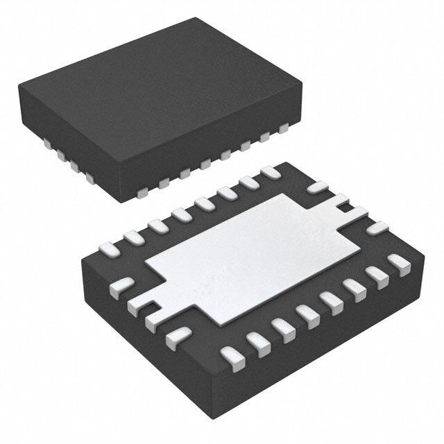
| 供应商器件封装 | 20-VQFN (3.5x4.5) |
| 其它名称 | 296-21643-6 |
| 功能 | 任何功能 |
| 包装 | Digi-Reel® |
| 单位重量 | 47.300 mg |
| 商标 | Texas Instruments |
| 安装类型 | 表面贴装 |
| 安装风格 | SMD/SMT |
| 封装 | Reel |
| 封装/外壳 | 20-VFQFN 裸露焊盘 |
| 封装/箱体 | VQFN-20 |
| 工作温度 | -40°C ~ 85°C |
| 工厂包装数量 | 250 |
| 带LED驱动器 | 无 |
| 带定序器 | 无 |
| 带监控器 | 无 |
| 拓扑 | 降压(降压)同步(1),线性(LDO)(1) |
| 最大工作温度 | + 85 C |
| 最小工作温度 | - 40 C |
| 标准包装 | 1 |
| 电压-电源 | 3 V ~ 28 V |
| 电压/电流-输出1 | 控制器 |
| 电压/电流-输出2 | 0.75 V ~ 3.3 V,2A |
| 电压/电流-输出3 | - |
| 类型 | DC/DC Controller |
| 系列 | TPS51511 |
| 输入电压 | 3 V to 28 V |
| 输出数 | 2 |
| 输出电压 | 0.75 V |
| 输出电流 | 10 A |
| 输出端数量 | 1 Output |
| 配用 | /product-detail/zh/TPS51511EVM/296-31170-ND/1907887 |
| 频率-开关 | 350kHz |


PDF Datasheet 数据手册内容提取
TPS51511 www.ti.com SLVS735A–FEBRUARY2007–REVISEDAPRIL2007 Synchronous Switcher Controller With 2-A LDO for GPU Power FEATURES – OptionalPGOOD • SwitcherController: – OutputDischarge – Adjustable-OutputBuckConverter,0.75V – ThermalShutdown to3.3V APPLICATIONS – WideInputVoltageRange:3.0-Vto28-V • GPUPower – D-CAP™Modewith100-nsLoadStep Response • NotebookComputers – CurrentModeOptionSupportsCeramic DESCRIPTION OutputCapacitors – CurrentSensingFromR orResistor The TPS51511 is a 350-kHz D-CAP-mode DS(ON) synchronous switcher with a 2-A, source-only low – InternalSwitchSupportsDynamicOutput drop-out (LDO) regulator. It is specifically designed VoltageChange for low cost/low noise/low external-component count – AdvancedPGOODMaskFeature power systems for GPU applications. The integrated – EquippedWithPGOOD,OVPandUVP 'OD' switch in the buck controller supports dynamic output voltage change. The current mode option of – OutputDischarge the synchronous buck converter can support pure – 5VUVLOProtection output ceramic-capacitor applications. The • LDORegulator: open-drain LDO power-good signal can be accessed through the OD pin when it is needed in the – 2-ALDOforGPUI/OPower application. The TPS51511 is available in the – InputRange:Upto5V thermally-enhanced 20-pin QFN package, and is – OutputRange:0.75Vto3.3V specifiedfrom–40(cid:176) Cto85(cid:176) C. – RequiresOnly20-m FCeramicOutput CapacitorforLDOOutput +1.8 V_LDOIN VI= 3 V to 28 V 1 20 PC+I 1E.2x pVre/ s2sA I/O 2 NC VLDOIN VBST DRVH19 ++11..12 VVG__PLPUoe_wrcfeoorrr mePaonwceer 3 VLDO LL 18 4 VLDOFB DRVL17 5 GND PGND16 TPS51511 6 ODOFF CS15 ODOFF = Lo, 1.2 V 7 OD V5IN 14 ODOFF = Hi, 1.1 V 8 COMP PGOOD13 B O +5 V 9 VOSW VSWF ENLD ENSW12 PGOOD 10 11 ENSW ENLDO Pleasebeawarethatanimportantnoticeconcerningavailability,standardwarranty,anduseincriticalapplicationsofTexas Instrumentssemiconductorproductsanddisclaimerstheretoappearsattheendofthisdatasheet. D-CAP,PowerPADaretrademarksofTexasInstruments. PRODUCTIONDATAinformationiscurrentasofpublicationdate. Copyright©2007,TexasInstrumentsIncorporated Products conform to specifications per the terms of the Texas Instruments standard warranty. Production processing does not necessarilyincludetestingofallparameters.
TPS51511 www.ti.com SLVS735A–FEBRUARY2007–REVISEDAPRIL2007 Thesedeviceshavelimitedbuilt-inESDprotection.Theleadsshouldbeshortedtogetherorthedeviceplacedinconductivefoam duringstorageorhandlingtopreventelectrostaticdamagetotheMOSgates. ORDERINGINFORMATION PACKAGED ORDERINGPART MINIMUMORDER T PINS OUTPUTSUPPLY ECOPLAN A DEVICES NUMBER QUANTITY TPS51511RHLT Small 250 –40(cid:176) Cto85(cid:176) C PLASTICRHL 20 Tape-and-Reel Green(RoHSand noSb/Br) TPS51511RHLR Tape-and-Reel 3000 ABSOLUTE MAXIMUM RATINGS overoperatingfree-airtemperaturerange(unlessotherwisenoted)(1) VALUE UNIT VBST –0.3to36 V VBST(3) –0.3to6 V V5IN,VLDOIN –0.3to6 V Inputvoltagerange(2) CS,VLDOFB,VOSW –0.3to6 V ENSW,ENLDO,VSWFB,ODOFF –0.3to6 V PGND –0.3to0.3 V DRVH –1.0to36 V LL –1.0to30 V Outputvoltagerange (2) DRVL –0.3to6 V VLDO,OD,COMP,PGOOD –0.3to6 V q Junction-to-Ambientthermalresistance 53.34 (cid:176) C/W JA Thermalinformation q Junction-to-PowerPADthermalresistance 8.84 (cid:176) C/W JC T Operatingambienttemperaturerange –40to85 (cid:176) C A T Operatingjunctiontemperaturerange –40to125 (cid:176) C J T Storagetemperature –55to150 (cid:176) C stg (1) Stressesbeyondthoselistedunderabsolutemaximumratingsmaycausepermanentdamagetothedevice.Thesearestressratings onlyandfunctionaloperationofthedeviceattheseoranyotherconditionsbeyondthoseindicatedunderrecommendedoperating conditionsisnotimplied.Exposuretoabsolute-maximum-ratedconditionsforextendedperiodsmayaffectdevicereliability. (2) Allvoltagevaluesarewithrespecttothenetworkgroundterminalunlessotherwisenoted. (3) VoltagevalueiswithrespecttotheLLterminal. RECOMMENDED OPERATING CONDITIONS overoperatingfree-airtemperaturerange(unlessotherwisenoted) MIN MAX UNIT Supplyvoltage V5IN 4.75 5.25 V VBST,DRVH –0.1 34 LL –0.6 28 Voltagerange VLDO,VLDOFB,VOSW –0.1 3.6 V PGND –0.1 0.1 ENSW,ENLDO,ODOFF,PGOOD,CS,COMP,DRVL,OD,VSWFB,VLDOIN –0.1 5.25 T Operatingfree-airtemperature –40 85 (cid:176) C A 2 SubmitDocumentationFeedback
TPS51511 www.ti.com SLVS735A–FEBRUARY2007–REVISEDAPRIL2007 ELECTRICAL CHARACTERISTICS overoperatingfree-airtemperaturerange,V =5V(unlessotherwisenoted) V5IN PARAMETER TESTCONDITIONS MIN TYP MAX UNIT SUPPLYCURRENT TA=25(cid:176)C;Noload, IV5IN1 Supplycurrent1,V5IN VENSW=VENLDO=5V, 0.8 2 mA COMPconnectedtocapacitor IV5IN2 Supplycurrent2,V5IN TCAO=M2P5(cid:176)cCo;nNneocltoeaddt,oVcEaNpSWac=it5o,rVENLDO=0V, 300 600 m A IV5IN3 Supplycurrent3,V5IN TA=25(cid:176)C;Noload,VENSW=5V,VENLDO=0,VCOMP=5V 240 500 m A IV5INSDN Shutdowncurrent,V5IN TVAEN=S2W5(cid:176)=CV;ENNoLDlOoa=d,0V 0.1 1.0 m A IVLDOIN1 Supplycurrent1,VLDOIN TVAEN=S2W5(cid:176)=CV;ENNoLDlOoa=d,5V 1 15 m A IVLDOIN2 Supplycurrent2,VLDOIN TA=25(cid:176)C;Noload,VENSW=0V,ENLDO=5V, 0.1 15 m A IVLDOINSDN Standbycurrent,VLDOIN TVAEN=S2W5(cid:176)=CV;ENNoLDlOoa=d,0V 0.1 1 m A LDO VLDOFB LDOfeedbackvoltage –40(cid:176)C<TA<85(cid:176)CVLDOIN=1.8V,VVLDOsetto1.2V 745.6 757 768.3 mV D VVLDO LDOloadregulation 00(cid:176)AC<<ITLDAO<<825(cid:176)AC,VLDOIN=2.5V(1),VVLDOsetto1.2V, 30 mV ILDOOC LDOcurrentlimit VcuLDrrOeInNt=un2t.i5liVti(s1),limVLitDeOd=1.2V,COUT=2· 10m F,Raisetheoutput 2 2.5 3.5 A IVLDOFBBIAS LDOfeedbackbiascurrent ENLDO=5V,VLDOIN=1.8V,VLDOFB=0.8V –1 –0.2 1 m A IVLDOFBLK LDOfeedbackleakcurrent ENLDO=0V,VLDOIN=1.8V,VLDOFB=0.8V –1 1 m A V2.V4L2D5OV=,2T.5A=V,2I5V(cid:176)LCDO=1A;ReduceVLDOINuntilVVLDOdropsto 0.18(2) RDS(ON) Seriesresistance V1.V7L4D6OV=,1T.8A=V,2I5V(cid:176)LCDO=1A;ReduceVLDOINuntilVVLDOdropsto 0.16(2) W V1.V1L6D4OV=,1T.2A=V,2I5V(cid:176)LCDO=1A;ReduceVLDOINuntilVVLDOdropsto 0.15(2) IVLDODischg VLDOdischargecurrent ENLDO=0V,VLDO=0.5V 10 17 40 mA OPENDRAINSWITCH Turnonthresholdvoltage 0.698 0.716 0.735 V VODOFFth1 Opendrainenablethreshold Hysteresis 38 mV voltage Secondthresholdvoltage 1.25 V VODOFFth2 Hysteresis 8 mV TODOFFth1delay Turnonthresholdvoltage‡ Turnoffthresholdvoltage 32 m s ROD Opendrainresistance TVAOD=O2FF5(cid:176)=C0;VVOD=0.5V, 13 50 W IODLEAK ODswitchcurrentleakage TA=25(cid:176)C;VODOFF=5V –1 1 m A IODOFFBIAS Opendrainenablebiascurrent TA=25(cid:176)C;VODOFF=5V –1 1 (1) Becauseofthevoltagedroponthecontactofthetestfixture,V issetat2.5V. LDOIN (2) Ensuredbydesign.Notproductiontested. SubmitDocumentationFeedback 3
TPS51511 www.ti.com SLVS735A–FEBRUARY2007–REVISEDAPRIL2007 ELECTRICAL CHARACTERISTICS (continued) overoperatingfree-airtemperaturerange,V =5V(unlessotherwisenoted) V5IN PARAMETER TESTCONDITIONS MIN TYP MAX UNIT VOSWOUTPUT TA=25°C 740.2 750 759.8 VVSWFB VSWFBregulationvoltage TA=0to85°C(3) 738.7 750 761.3 mV TA=-40to85°C(3) 738.0 750 762.0 RVOSW Inputimpedance,VOSW 750 kW VSWFB=0.78V,COMP=open –0.04 m A IVSWFB Inputcurrent,VSWFB VSWFB=0.78V,COMP=5V –0.06 m A IVOSWDischg Dischargecurrent,VOSW ENSW=0V,VOSW=0.5V 8 15 35 mA TRANSCONDUCTANCEAMPLIFIER gm Gain TA=25(cid:176)C 240 300 360 m S ICOMPSNK COMPmaximumsinkcurrent ECNOLMDPO==10.2V8,VENSW=5V,VSWFB=0V,VOSW=1.94V, 13 m A ICOMPSRC COMPmaximumsourcecurrent ECNOLMDPO==10.2V8,VENSW=5V,VSWFB=0V,VOSW=1.66V, –13 m A VCOMPHI COMPhighclampvoltage ENLDO=0V,ENSW=5V,VSWFB=0V,CS=0V,VOSW=1.66V 1.31 1.34 1.37 V VCOMPLO COMPlowclampvoltage ENLDO=0V,ENSW=5V,VSWFB=0V,CS=0V,VOSW=1.94V 1.18 1.21 1.24 V DUTYCONTROL TON Operationontime VIN=12V,VOSW=1.8V 400 ns TON0 Startupontime VIN=12V,VOSW=0V 125 ns TONMIN Minimumontime TA=25(cid:176)C 100 ns TOFFMIN Minimumofftime TA=25(cid:176)C 350 ns OUTPUTDRIVERS RDRVH DRVHresistance Source,IDRVH=-100mA 3 6 W Sink,IDRVH=100mA 0.9 3 RDRVL DRVLresistance Source,IDRVL=-100mA 3 6 W Sink,IDRVL=100mA 0.9 3 DRVH-offtoDRVL-on(3) 10 TD Deadtime DRVL-offtoDRVH-on(3) 30 ns INTERNALBSTDIODE VFBST Forwardvoltage VV5IN-VBST,IF=10mA,TA=25(cid:176)C 0.7 0.8 0.9 V IVBSTLK VBSTleakagecurrent VVBOSSTW==314.8V7,LVL,T=A2=82V5,(cid:176)C 0.1 1 m A ZEROCURRNTCOMPARATOR VZC Zerocurrentcomparatoroffset –10 0 10 mV (3) Ensuredbydesign.Notproductiontested. 4 SubmitDocumentationFeedback
TPS51511 www.ti.com SLVS735A–FEBRUARY2007–REVISEDAPRIL2007 ELECTRICAL CHARACTERISTICS (continued) overoperatingfree-airtemperaturerange,V =5V(unlessotherwisenoted) V5IN PARAMETER TESTCONDITIONS MIN TYP MAX UNIT PROTECTION VPGND-CSvoltage,PGOOD=Hi, 50 60 70 VCS<0.5V VOCL Currentlimitthreshold mV VPGND-CSvoltage,PGOOD=Lo, 20 30 40 VCS<0.5V ITRIP CSsinkcurrent VVCRSDS>(O4N.)5CSV>,P4G.5OVO,DPG=OHOi,DTA==Lo2,5T(cid:176)CA=25(cid:176)C 94 150 161 m A TCITRIP TcoReIPfficciuernrtenttemperature sOennstheesbcahseimseo,f25(cid:176)C 4500 ppm/(cid:176)C VOCLoff OCPcomp.offset (VV5IN-CS–VPGND-LL)voltage,VV5IN-CS=60mV,VCS>4.5V –10 0 10 mV Currentlimitthresholdsetting VRtrip range V5IN-CSvoltage(4) 30 150 mV POWERGOODCOMPARATOR PGoutfromlowend 87% 90% 93% VTVoPG VOSWPGThreshold PGoutfromhighend 107% 110% 113% PGhysteresis 5% IPGMAX PGSinkCurrent VLDO=0V,VPGOOD=0.5V 2.5 7.5 mA TPGDEL PGOODDelay DelayforPGin 80 130 200 m s VOSWthresholdvoltagefor turningonPGOODuplimitand 1.36 V OVPfeature VVOSWTH VOSW=1.5V VOSWthresholdhysteresis voltageforturningonPGOODup 10 mV limitandOVPfeature UVLO/LOGICTHRESHOLD Wakeup 3.7 4.0 4.3 VUVV5IN V5INUVLOthreshold V Hysteresis 0.15 0.225 0.3 VIH High-levelinputvoltage ENLDO,ENSW 2.2 V VIL Low-levelinputvoltage ENLDO,ENSW 0.3 V VIHYS Hysteresisvoltage ENLDO,ENSW 0.2 V IINLEAK Logicinputleakagecurrent ENLDO,ENSW –1 1 m A IINVSWFB IVnSpWutFLBea-1ka1ge/BiasCurrent –1 1 m A PROTECTION:UVPANDOVP VOVP VOSWOVPtripthreshold OVPdetect 110% 115% 120% TOVPDEL VOSWOVPpropdelay See(4) 1.5 m s VUVP OutputUVPtripthreshold UVPdetect 70% TUVPDEL OutputUVPpropdelay 32 clks TUVPEN OutputUVPenabledelay 1007 clks THERMALSHUTDOWN Shutdowntemperature(4) 160 TSDN ThermalSDNthreshold Hysteresis(4) 10 (cid:176)C (4) Ensuredbydesign.Notproductiontested. SubmitDocumentationFeedback 5
TPS51511 www.ti.com SLVS735A–FEBRUARY2007–REVISEDAPRIL2007 DEVICE INFORMATION TOPVIEW RHLPACKAGE V L D V O B IN ST 1 20 NC 2 19 DRVH VLDO 3 18 LL C O VLDOFB 4 MP 17 DRVL GND 5 16 PGND TPS51511 ODOFF 6 15 CS OD 7 14 V5IN COMP 8 13 PGOOD VOSW 9 12 ENSW 10 11 V E S N W L FB DO TERMINALFUNCTIONS TERMINAL I/O DESCRIPTION NAME NO. VLDOIN 1 I InputterminaloftheLDO. NC 2 – Pinnotused.Nointernalconnection. VLDO 3 O OutputterminaloftheLDO.WhenLDOisturnedoff,theoutputcapacitorisdischargedbyaninternalFET. VLDOFB 4 I FeedbackpinoftheLDO.AvoltagedividersetstheLDOoutputvoltage. GND 5 – Signalground.ConnecttonegativeterminaloftheLDOoutputcapacitor. Acomparatorinput.WhenthispinistiedtoVLDOFB,ODactsasaPGOODsignalfortheLDO.When ODOFF 6 I connectedtoexternallogic,ODactslikeaswitch.SeeTable1fordetailedinformation. OD 7 I/O Theoutputofthemultifuntionalopen-drainswitch. Outputofthetransconductanceamplifierforphasecompensationincurrentmode.ConnecttoV5INtodisable COMP 8 I/O GmamplifierandenableD-CAPmode. VOSW 9 I/O Switcheroutputvoltagemonitor.Inputforon-timeone-shottimerandadvancedPGOODmaskingcomparator. Feedbackpinoftheswitcher.Avoltagedividerconnectedtothispinsetstheswitcheroutputvoltage.Aresistor connectedbetweenthispinandODpincanbeinsertedinparallelwiththelow-sideresistorofthevoltage VSWFB 10 I divider,accordingtotheODOFFinput,toestablishthedynamicvoltagestep.Thisterminalisalsotheinputfor theOVP,UVPandPGOODcomparators. ENLDO 11 I LDO-enablesignalinput. ENSW 12 I Switcher-enablesignalinput. Power-goodsignalopen-drainoutput.PulledlowwhenVSWFBvoltagefallsoutsidethetargetwindow PGOOD 13 O comparator.TheuppersideofthewindowcomparatorwillbemaskediftheVOSWvolttageislowerthan1.36V (typ.).RefertotheAdvancePGOODMasksectionfordetails. 5VPowersupplyinput.This5Vsuppliesinternalcontrolcircuitry,LDOpassFETgatedrive,VDRVHand V5IN 14 I VDRVLgatedrivers. Current-sensecomparatorinput(–)forresistorcurrent-sensemode.Ifconnectedto5VINthrougha CS 15 I/O voltage-settingresistor,constantcurrentsinksthroughthispintosettheOCLpointfortheR DS(ON) current-sensemode. PGND 16 I/O GroundforbottomMOSFETgatedriver.Alsocurrent-sensecomparatorinput(+). DRVL 17 O Rectifying(bottom)MOSFETgate-driveoutput. LL 18 I/O Switching(top)MOSFETgatedriverreturn.Currentsensecomparatorinput(–)forR current-sensemode. DS(ON) DRVH 19 O Switching(top)MOSFETgatedriveoutput VBST 20 I/O Switching(top)MOSFETdriverbootstrapvoltageinput.InternallyconnectedtoV5INthroughanPNdiode. 6 SubmitDocumentationFeedback
TPS51511 www.ti.com SLVS735A–FEBRUARY2007–REVISEDAPRIL2007 TYPICAL CHARACTERISTICS V5INSUPPLYCURRENTvsTEMPERATURE V5INSHUTDOWNCURRENTvsTEMPERATURE 2 1 1.80 0.90 A 1.60 Am 0.80 nt 1 - m 1.40 urrent - 0.70 y Curre 1.201 down C 00..5600 - Suppl5IN1 00..6800 - ShutNSDN 00..3400 IV 0.40 V5I 0.20 I 0.20 0.10 0 0 -50 0 50 100 150 -50 0 50 100 150 TJ- Junction Temperature - °C TJ- Junction Temperature - °C Figure1. Figure2. VLDOINSUPPLYCURRENTvsTEMPERATURE CSCURRENTvsTEMPERATURE 5 16 4.50 14 PGOOD = Hi 4 12 Am 3.50 A ply Current - 2.503 S Current -m 108 PGOOD = Lo p 2 C I- SuCC1.50 I- (trip) 46 1 0.50 2 0 0 -50 0 50 100 150 -50 0 50 100 150 TJ- Junction Temperature - °C TJ- Junction Temperature - °C Figure3. Figure4. VOSWDISCHARGECURRENTvsTEMPERATURE VLDODISCHARGECURRENTvsTEMPERATURE 30 30 - Discharge Current - mAWDISCHG12215500 - Discharge Current - mADODISCHG 122505 S 5 L O V V I I 0 10 -50 0 50 100 150 -50 0 50 100 150 TJ- Junction Temperature - °C TJ- Junction Temperature - °C Figure5. Figure6. SubmitDocumentationFeedback 7
TPS51511 www.ti.com SLVS735A–FEBRUARY2007–REVISEDAPRIL2007 TYPICAL CHARACTERISTICS (continued) OVP,UVPTHRESHOLDvsTEMPERATURE SWITCHINGFREQUENCYvsINPUTVOLTAGE 140 450 IOSW= 5A, 400 VI= 4V - 28 V, VO= 1.2 V % 120 VOVP kHz 350 - Threshold - UVP 100 hing Frequency - 223050000 , VP witc 150 V S VO 80 VUVP - SW 100 f 50 60 0 -50 0 50 100 150 4 8 12 16 20 24 28 TJ- Junction Temperature - °C VI- Input Voltage - V Figure7. Figure8. SWITCHINGFREQUENCYvsOUTPUTCURRENT VOSWLOADREGULATION 450 1.220 VI= 12 V, IVOSW= 1 mA- 10A, 400 VO= 1.2 V 1.215 VI= 12 V, Hz 350 VO= 1.2 V - Switching Frequency - k 122350500000 V- Output Voltage - VO 111...1221901.5502 SW 100 1.190 f 50 1.185 0 1.180 0 2 4 6 8 10 0 2 4 6 8 10 IO- Output Current -A IO- Output Current -A Figure9. Figure10. VOSWLINEREGULATION LDOLOADREGULATIONAT1.5VINPUT 1.240 1.21 1.230 VI= 4 V - 28 V, VLDOIN= 1.5 V VO= 1.2 V 1.2 V 1.220 V 1.19 TA= -40°C Voltage - 1.210 Voltage - 1.18 Output 1.119.02 Output 1.17 TA= 25°C V- O 1.180 V- O1.16 TA= 85°C 1.170 1.15 1.160 1.14 4 8 12 16 20 24 28 0 0.5 1 1.5 2 VI- Input Voltage - V IL- Load Currents -A Figure11. Figure12. 8 SubmitDocumentationFeedback
TPS51511 www.ti.com SLVS735A–FEBRUARY2007–REVISEDAPRIL2007 TYPICAL CHARACTERISTICS (continued) LDOLOADREGULATIONAT1.8VINPUT VOSWEFFICIENCY 1.21 100 IO= 1 mA- 10A, 1.2 TA= -40°C VO= 1.2 V VI= 12 V 90 VI= 8 V V 1.19 TA= 25°C e - ag % 80 - Output Volt 11..1178 TA= 85°C Efficiency - 70 VI= 20 V VO1.16 60 1.15 VLDOIN= 1.8 V 1.14 50 0 0.5 1 1.5 2 0.001 0.01 0.1 1 10 IL- Load Currents -A IO- Current -A Figure13. Figure14. RIPPLEWAVEFORMS,HEAVYLOADCONDITION VOSWLOADTRANSIENTRESPONSE t - Time - 4ms/div t - Time - 20ms/div Figure15. Figure16. VLDOLOADTRANSIENTRESPONSE VOSWSTART-UPWAVEFORMS t - Time - 10ms/div t - Time - 100ms/div Figure17. Figure18. SubmitDocumentationFeedback 9
TPS51511 www.ti.com SLVS735A–FEBRUARY2007–REVISEDAPRIL2007 TYPICAL CHARACTERISTICS (continued) VOSWSHUT-DOWNWAVEFORMS VLDOSTART-UPWAVEFORMS t - Time - 20 ms/div t - Time - 20ms/div Figure19. Figure20. VLDOSHUT-DOWNWAVEFORMS VOSWBODEPLOT(CURRENTMODE) 80 180 60 135 Phase 40 90 20 45 g Gain - dB 0 Gain 0 hase - de -20 -45P -40 -90 -60 -135 -80 -180 100 1K 10K 100K 1M f - Frequency - Hz t - Time - 1 ms/div Figure21. Figure22. DYNAMICVOLTAGESTEP-UPWAVEFORMS DYNAMICVOLTAGESTEP-DOWNWAVEFORMS t - Time - 40ms/div t - Time - 40ms/div Figure23. Figure24. 10 SubmitDocumentationFeedback
TPS51511 www.ti.com SLVS735A–FEBRUARY2007–REVISEDAPRIL2007 FUNCTIONAL BLOCK DIAGRAM ENLDO LDO_ON V5IN VLDO + V5INOK 3.7V/3.5V ENSW SW_ON GND + Ref RefOK VOSW 0.7V OD + Ref GND 1.25V 1.25V + GND GND S0 S1 OUT 1.36V + 0 0 A ODOFF 0 1 B 1 0 C 1 1 D + 0.716V VLDOIN + OUT 0.75V+5/10% + PGOOD 0.678V High(1) A B Delay C PGOOD Delay 45us + D VLDO 1 0.75V-5/10% VOSWOK PGND S0 S1 VLDOFB 0 UVP + Loop path LDO_ON SW_ON 0.75V-30% + 0.75V control VSWFB OVP + + + 0.75V Ref PWM 0.75V+15% + VOSWOV VOSW V5IN LL VOSWUV V5IN COMP V5IN VOSWOK 60/30mV + VBST OCP DRVH + 1shot LL XCON 10/5uA V5IN DRVL GND + VOSWOK ZC PGND CS LL + Ref VOSW + 4V SubmitDocumentationFeedback 11
TPS51511 www.ti.com SLVS735A–FEBRUARY2007–REVISEDAPRIL2007 DESCRIPTION TPS51511 is an integrated power-management solution that combines a synchronous buck controller and a high-current, source-only, low-dropout linear regulator (LDO) in a small 20-pin QFN package. Each output provides voltages required by typical graphic-system applications. The switching-mode power supply portion employs external N-channel MOSFETs to provide high current for a GPU core. The output voltage is adjustable from 0.75 to 3.3 V with an external divider. The input voltage range of the switcher is 3 V to 28 V. The switcher uses adaptive on-time PWM under heavy load conditions, and automatically reduces the frequency under light loads to achieve excellent efficiency down to several mA. The output of the switcher is sensed by the VOSW pin to generate the on-time pulse, with the voltage of V sensed by LL pin. The current sensing uses either the IN R oftheexternalrectifyingMOSFETforalow-cost,losslesssolution,orasenseresistorplacedinseries to DS(ON) therectifyingMOSFETforapplicationsneedingamoreaccuratecurrentlimit. TheLDOcansourceupto2ADCcurrentwithonly20m F(two10m Finparallel)ceramicoutputcapacitors. VOSW Switcher, Dual PWM Operation Modes The main control loop of the switcher is designed as an adaptive on-time pulse width modulation (PWM) controller. It supports two control schemes; a current mode and a proprietary D-CAP mode. D-CAP mode does not require an external compensation circuit, and is suitable for low external component count configurations using output capacitor(s) with an appropriate ESR value. Current-mode control has more flexibility, using an external compensation network, and can be used to achieve stable operation with very low-ESR capacitors such asceramiccapacitors. These control modes are selected by the COMP terminal connection. If the COMP pin is connected to V5IN, the TPS51511 is in D-CAP Mode. If the COMP pin is connected to the RC compensation network, the device operatesincurrentmode. At the beginning of each cycle, the synchronous top MOSFET is turned on (ON state). This MOSFET is turned off (OFF state) after the internal one-shot timer expires. The on-time issued by this one-shot is proportional to the ratio of V to V . In this way, the switching frequency can be kept reasonably constant over the OUT IN input-voltage range, hence it is called adaptive on-time control (see PWM frequency and Adaptive On-time Control). The MOSFET is turned on again when the feedback information indicates insufficient output voltage and the inductor current is below the overcurrent limit. By repeating operation in this manner, the controller regulates the output voltage. The synchronous bottom, or the rectifying MOSFET, is turned on during each OFF state to minimize conduction loss. The rectifying MOSFET is turned off when the inductor current indicates zero voltage level. This enables seamless transition to the reduced frequency operation under light load conditions so thatthehighefficiencyismaintainedoverthebroadrangeofloadcurrents. In the current-mode control scheme, the transconductance amplifier generates a target current level corresponding to the voltage difference between the feedback point and the internal 750-mV reference. During the OFF state, the PWM comparator monitors the inductor-current signal as well as the target current level, and whenthe inductor-current signal goes lower than the target current level, the comparator asserts the SET signal, switching the system to the ON state. The voltage-feedback gain is adjustable outside the controller IC to supportvarioustypesofoutputMOSFETsandcapacitors.IntheD-CAPMode,thetransconductanceamplifier is disabled and the PWM comparator directly compares the feedback-point voltage to the internal 750-mV reference during the OFF state. When the feedback point becomes lower than the reference voltage, the comparatorassertstheSETsignal,triggeringtheONstate. 12 SubmitDocumentationFeedback
TPS51511 www.ti.com SLVS735A–FEBRUARY2007–REVISEDAPRIL2007 VOSW Switcher, Light Load Condition TPS51511 automatically reduces the switching frequency under light load conditions to maintain high efficiency. This frequency reduction is achieved smoothly and without increasing the V ripple or affecting the load OUT regulation. As the output current decreases from a heavy load condition, the inductor current is also reduced and eventually comes to the point that its ripple-valley value decreases down to zero current, which is the boundary between continuousconductionanddiscontinuousconductionmodes.The rectifying MOSFET will be turned off when this zero inductor current is detected. As the load current decreases further, the converter runs in discontinuous-conduction mode, and takes longer to discharge the output capacitor to the level that will issue the next ON cycle. The ON time is kept the same as that in the heavy load condition. Conversely, when the output current increases from a light load to a heavy load, the switching frequency increases to the constant 350 kHz as the inductor current reaches continuous conduction. The transition point between light and heavy-load operation I (i.e., the threshold between continuous and discontinuous conduction mode) can be calculated OUT(LL) asfollows; 1 (cid:4)VIN(cid:2)VOUT(cid:5)(cid:1)VOUT IOUT(LL)(cid:3)2(cid:1)L(cid:1)ƒ(cid:1) VIN (1) WherefisthePWMswitchingfrequency,350kHz. The switching frequency versus the output current in the light load condition is a function of L, f, V and V , IN OUT but it decreases almost proportionally to the output current from the I given above. For example, it will be OUT(LL) 35kHzatI /10and3.5kHzatI /100. OUT(LL) OUT(LL) Low-Side Driver The low-side driver is designed to drive high current low R N-channel MOSFETs. The drive capability is DS(ON) represented by its internal resistance, 3 W for V5IN to DRVL, and 0.9 W for DRVL to PGND. A dead time to prevent shoot-through is internally generated between the top MOSFET off to bottom MOSFET on, and bottom MOSFETofftotopMOSFETon.The5-VbiasvoltageisdeliveredfromV5INsupply. The instantaneous drive current is supplied by an input capacitor connected between V5IN and GND. Add a ceramic capacitor with a value between 1.0 m F and 4.7 m F placed close to the V5IN pin to stabilize the 5-V output from any parasitic impedance from the supply. The average drive current is equal to the gate charge at V =5 V condition, times the switching frequency. This gate-drive current as well as the high-side gate-drive GS currenttimes5VaccountsforthepowerthatmustbedissipatedfromtheTPS51511package. High-Side Driver The high-side driver is designed to drive high-current, low R N-channel MOSFET(s). It is configured as a DS(ON) floating driver, with the 5-V bias voltage delivered from the V5IN supply. The average drive current is also calculated by the gate charge at V =5 V condition, times switching frequency. The instantaneous drive current GS is supplied by the flying capacitor between VBST and LL pins. The drive capability is represented by its internal resistance,3W forVBSTtoDRVH,and0.9W forDRVHtoLL. Current Sensing Scheme To support both high-accuracy and low-cost current sensing applications, TPS51511 supports two different currentsensingschemes;external-resistorsensing,andrectifying-MOSFETR sensing. DS(ON) In the resistor-sensing scheme, an appropriate current-sensing resistor is connected between the source terminal of the rectifying MOSFET and PGND, and the CS pin is connected to the rectifying MOSFET source terminalnode.TheinductorcurrentismonitoredbythevoltagebetweenPGNDpinandCSpin. In the R -sensing scheme, the CS pin is connected to the V5IN pin through the trip-voltage setting resistor DS(ON) R . In this case, the CS terminal sinks the 10-m A I current, and the trip level is set to the voltage across TRIP TRIP R . The inductor current is monitored by the voltage between the PGND pin and the LL pin, so the LL pin is TRIP connected to the drain terminal of the rectifying MOSFET. I has a 4500-ppm/(cid:176) C temperature slope to TRIP compensatethetemperaturedependencyoftheR . DS(ON) In either scheme, PGND is used as the positive current-sensing node, so PGND must be connected to the propercurrent-sensingdevice,i.e.,thesenseresistororthesourceterminaloftherectifyingMOSFET. SubmitDocumentationFeedback 13
TPS51511 www.ti.com SLVS735A–FEBRUARY2007–REVISEDAPRIL2007 PWM Frequency and Adaptive On-Time Control TPS51511 employs an adaptive on-time control scheme, and does not have a dedicated oscillator on board. However, the device runs with a fixed 350kHz pseudo-constant frequency by feed-forwarding the input and output voltage into the on-time one-shot timer. The on-time is inversely proportional to the input voltage and proportional to the output voltage so that the duty-cycle ratio is kept the same as V /V in the same cycle OUT IN time. Although the TPS51511 does not have a pin connected to V , the input voltage is monitored at the LL pin IN during the ON state. This reduces the pin count in order to make the part compact without sacrificing its performance. In order to secure minimum ON time during startup, the feed-forward feature from the output voltageisenabledaftertheoutputvoltagebecomes750mVorhigher. Soft-Start and Powergood (PGOOD) The soft-start function of the switcher is achieved by ramping up the reference voltage and a two-stage current clamp. At the starting point, the reference voltage is set to 650 mV (87% of its target value), and the overcurrent threshold is set to half of the nominal value. When the UVP comparator detects an VOSW voltage greater than 80% of the target, the reference begins to ramp up and reaches 750 mV after 85 m s. 45 m s after the voltage becomes good, the power-good comparator releases the overcurrent threshold to the nominal value. TPS51511 turnsoffthepower-goodopen-drainMOSFETwhenVOSWreachesthegoodstate. The soft-start function of the LDO is achieved by clamping the current during startup. The threshold of the current limit is set to 2.5 A (typical). TPS51511 has an independent window comparator for each output, but the PGOOD signal indicates only the status of VOSW. If a separate powergood signal is needed for the LDO, see ODandODOFFforconfigurationdetails. Thesoft-startdurations,T ,T arefunctionsofoutputcapacitances. VOSW VLDO 2(cid:1)C (cid:1)V T (cid:3) VOSW VOSW(cid:2)80(cid:1)s VOSW I VOSWOCP (2) Where,I isthecurrentlimitvaluefortheVOSWswitchercalculatedbyEquation5. VOSWOCP C (cid:1)V T (cid:2) VLDO VLDO VLDO I VLDOOCL (3) Where,I =2.5A(typical). VLDOOCL In both equations, no load current during startup is assumed. Note that both the switcher and the LDO do not startuptotargetvoltagewithfullloadconditions. EnableandDischarge Both the switcher and LDO can be enabled by bringing the voltage on the ENSW and ENLDO pins above 2.2 V, and disabled by pulling the voltage of ENSW and ENLDO down to 0.3 V. Both the switcher and LDO have output-discharge feature. The output is discharged through an internal MOSFET when the channel is disabled. Discharge continues until the output voltage is discharged below 0.3 V. In UVP or OVP conditions of the switching power supply, the device is latched off and the discharge is enabled until the output voltage drops below0.3V. 14 SubmitDocumentationFeedback
TPS51511 www.ti.com SLVS735A–FEBRUARY2007–REVISEDAPRIL2007 Current Protection for VOSW Theswitcherhascycle-by-cyclecurrent-limitcontrol.TheinductorcurrentismonitoredduringtheOFFstate, and the controller keeps the OFF state while the inductor current is larger than the overcurrent trip level. The trip leveland current-sense scheme are determined by the CS pin connection (see Current Sensing Scheme). In the resistor sensing scheme, the trip level, V , is a fixed value of 60 mV. In the R sensing scheme, the CS TRIP DS(ON) terminalsinks10m AandthetriplevelissettothevoltageacrosstheR resistor. TRIP V (mV)(cid:2)R (k(cid:1))(cid:1)10((cid:2)A) TRIP TRIP (4) Because the comparison is done during the OFF state, V sets the valley level of the inductor current. Thus, TRIP theloadcurrentattheovercurrentthreshold,I ,canbecalculatedasfollows; ocp V I V 1 (V -V )´V I = TRIP + RIPPLE = TRIP + ´ IN OUT OUT OCP R 2 R 2´L´f V DS(ON) DS(ON) IN (5) In an overcurrent condition, the current to the load exceeds the current to the output capacitor, thus the output voltage tends to fall. If the output voltage becomes less than power-good level, the V level is cut in half, and TRIP the output voltage tends to be even lower. Eventually, it will end up crossing the undervoltage-protection thresholdandbeshutdown. Over/Under Voltage Protection for VOSW The TPS51511 monitors the feedback voltage to detect overvoltage and undervoltage conditions. When the feedback voltage becomes higher than 115% of the target voltage, the OVP comparator output goes high, and the circuit latches the top MOSFET driver OFF and the bottom MOSFET driver ON. The TPS51511 also monitors the VOSW voltage directly, and if it becomes greater than 4 V, TPS51511 turns off the top MOSFET driver. When the feedback voltage becomes lower than 70% of the target voltage, the UVP-comparator output goes high, and an internal UVP delay counter starts. After 32 switching cycles, the TPS51511 latches OFF both top and bottom MOSFETs. This function is enabled after 1007 cycles from switcher startup to ensure proper startup. V5INUVLOProtection TPS51511 has V5IN under voltage lock out protection (UVLO). When the V5IN voltage is lower than the UVLO thresholdvoltage,theswitcherandLDOareshutoff.Thisisanon-latchingprotection. LDO Operation The TPS51511 integrated LDO is a source-only 2- A LDO. It has a typical current limit of 2.5 A . It can be separately enabled via the ENLDO pin, and the output voltage is set via the external voltage divider. Only a 20 m F ceramic capacitor (2· 10m F) is needed for this LDO. The transient response is very fast due to the wide bandwidthdesignoftheLDOfeedbackloop. The LDO has an internally fixed constant overcurrent limit of 2.5 A. This is a trailing current limit with no shutdownfunction. Thermal Shutdown The TPS51511 monitors its internal temperature. If the temperature exceeds the threshold value (typically 160(cid:176) C), the switcher and LDO are shut off. This is a non-latching protection, and operation is resumed when the deviceiscooleddownbyapproximately10(cid:176) C. Dynamic Voltage Step, OD and ODOFF OD and ODOFF are multifunction pins. By connecting the OD pin through a resistor to VSWFB, ODOFF is connected to an external control logic signal which can control OD to switch in and out this resistor in parallel with the bottom resistor of the voltage divider. This can dynamically change the switcher output voltage during operation. If the application requires a power-good signal for the LDO rather than switcher dynamic voltage control, OD and ODOFF can be configured to support the LDO power-good feature by connecting ODOFF to VLDOFB. In this mode, connect OD through a pullup resistor to the bias voltage (i.e. 5 V, 3.3 V) to act as the LDO power-good output. The functions of ODOFF and OD pin combinations related to the ENLDO and ENSW pinvoltagelevelsareshowninTable1. SubmitDocumentationFeedback 15
TPS51511 www.ti.com SLVS735A–FEBRUARY2007–REVISEDAPRIL2007 Table1.ODandODOFFFunctions ENLDO ENSW ODOFF(1) OD(2) Applications(3) >1.25V Off D 0.716V<ODOFF<1.25Vandlastslongerthan45m s Off D&G Hi X 0.716V<ODOFF<1.25Vandlastslessthan45m s KeepState G 0.678V<ODOFF<0.716V KeepState G <0.678V On D&G >1.25V Off D Lo Hi <1.25V On D&G Lo Lo X On G (1) Allvoltagesaretypicalvalues. (2) "Keepstate"meansnostatechangewithpreviousstate,“On”meansopendrainMOSFETisturnedonandODisconnectedtoground throughthisMOSFET.“Off”meansopendrainMOSFEToff. (3) “D”standsfordynamicvoltagechange“G”standsforLDOPGOOD. Advanced PGOOD Mask The advanced PGOOD mask feature allows the switcher to dynamically change the output voltage while maintainingthePGOODandOVPfunctionsduringthetransition. During the dynamic voltage change, if the output voltage is lower than 1.36 V (typ) the high-end PGOOD comparator and OVP comparator is masked. If the output voltage is set equal to or higher than 1.36 V (typ), the blanking circuit is disabled, and the high-end PGOOD threshold is set to 110%, and the OVP threshold is set to 115% of the output-voltage setting . When dynamic voltage change is implemented, a 1-nF ceramic capacitor mustbeaddedinparallelwiththetopresistorofthevoltagedividerasshowninFigure27. APPLICATION INFORMATION LOOP COMPENSATION AND EXTERNAL PARTS SELECTION CurrentModeOperation A buck converter using TPS51511 current mode operation can be partitioned into three portions, a voltage divider, an error amplifier and a switching modulator. By linearizing the switching modulator, we can derive the transfer function of the whole system. Since the current-mode scheme directly controls the inductor current, the modulatorcanbelinearizedasshowninFigure25. Voltage Divider VOSW R1 Gm = 300mS VIN Filter R2 DRVH Control Ref Logic Lx 0.75 V PWM and Driver DRVL ESR COMP R CS L Rc Ro = 75 M C O R Cc2 S PGND Cc ErrorAmplifier Switching Modulator Figure25.SimplifiedCurrent-ModeFunctionalBlocks In this representation, the inductor is located inside the local feedback loop, and its inductance does not appear in the small-signal model. As a result, a modulated current source including the power inductor can be modeled 16 SubmitDocumentationFeedback
TPS51511 www.ti.com SLVS735A–FEBRUARY2007–REVISEDAPRIL2007 APPLICATION INFORMATION (continued) as a current source with its transconductance of 1/Rs, and the output capacitor represents the modulator portion. This simplified model is applicable in the frequency space up to approximately half the switching frequency. Although the inductance has no influence in the small-signal model, it influences the large-signal model by limiting the slew rate of the current source. This means that the buck converter’s load-transient response, one of the large signal behaviors, can be improved by using a smaller inductance without affecting loopstability. Thetotalopen-looptransferfunctionofthewholesystemisgivenby H(s) =H (s)´H (s)´H (s) 1 2 3 (6) AssumingRL>>ESR,Ro>>RcandCc>>Cc2,thetransferfunctionofeachblockis R H1(s)(cid:2) 2 (cid:3)R2(cid:1)R1(cid:4) (7) Ro(1+s´Cc´Rc) H (s)=-Gm´ 2 (1+s´Cc´Ro)(1+s´Cc2´Rc) (8) H (s)(cid:3)1(cid:2)s(cid:1)Co(cid:1)ESR(cid:1)RL 3 1(cid:2)s(cid:1)Co(cid:1)RL Rs (9) TherearethreepolesandtwozerosinH(s).Eachpoleandzeroisgivenby w =1/(Cc· Ro) w =1/(Co· RL) w =1/(Cc2· Rc) p1 p2 p1 w =1/(Cc· Rc) w =1/(Co· ESR) z1 z2 Usually, each frequency of the poles and zeros is lower than the 0dB frequency, f . However, the f should be 0 0 kept under 1/3 of the switching frequency to avoid the effect of switching-circuit delay. The f is given by 0 Equation10. R ƒ (cid:3) 1 (cid:1) 1 (cid:1)Gm(cid:1)Rc(cid:3) 1 (cid:1)0.75(cid:1)Gm(cid:1)Rc o 2(cid:1) R (cid:2)R Co Rs 2(cid:1) Vout Co Rs 1 2 (10) Basedonthesmall-signalanalysisabove,theexternalcomponentscanbeselectedbythefollowingsteps: 1. Choosetheinductor. The inductance value should be determined to give a ripple current of approximately 1/4 to 1/3 of the maximumoutputcurrent. 1 (cid:4)VIN(max)(cid:2)VOUT(cid:5)(cid:1)VOUT 3 (cid:4)VIN(max)(cid:2)VOUT(cid:5)(cid:1)VOUT L(cid:3)IIND(ripple)(cid:1)ƒ(cid:1) VIN(max) (cid:3)IOUT(max)(cid:1)ƒ(cid:1) VIN(max) (11) The inductor also needs low DCR to achieve good efficiency, as well as enough room above peak inductorcurrentbeforesaturation.Thepeakinductorcurrentcanbeestimatedasfollows. V 1 (V -V )´V I = trip + ´ IN(max) OUT OUT IND(peak) R L´f V DS(ON) IN(max) (12) 2. Choosetherectifying(bottom)MOSFET. When the R sensing scheme is selected, the rectifying MOSFET’s on-resistance is used as this Rs so DS(ON) that lower R does not always promise better performance. In order to clearly detect inductor current, DS(ON) minimum Rs recommended is to give 15 mV or larger ripple voltage with the inductor ripple current. This will provide smooth transitions from CCM to DCM or vice versa. The upper side of the R is of course DS(ON) restricted by the efficiency requirement, and usually this resistance affects efficiency more at high load conditions. When using external-resistor current sensing, there is no restriction for low R . However, the current DS(ON) sensingresistanceRsitselfaffectstheefficiency. 3. Choosetheoutputcapacitor(s). Whenusingorganicsemiconductorcapacitors(OS-CON)orspecialtypolymercapacitors(SP-CAP), the ESR SubmitDocumentationFeedback 17
TPS51511 www.ti.com SLVS735A–FEBRUARY2007–REVISEDAPRIL2007 APPLICATION INFORMATION (continued) to achieve required ripple value at stable state or transient load conditions will determine the number and size of capacitor(s) needed, and the resulting capacitance will then be enough to satisfy stable operation. The peak-to-peak ripple value can be estimated by ESR times the inductor ripple current for stable state, or ESRtimestheload-currentstepforafasttransient-loadresponse. Ceramic capacitors typically have ESR values small enough to meet the ripple requirement. On the other hand, transient undershoot and overshoot driven by output capacitance will become the key factor to determinethecapacitance. 4. Determinef andcalculateRcusingEquation13. 0 Rc(cid:2)2(cid:1)(cid:1)ƒ (cid:1)Vout(cid:1) Co (cid:1)Rs 0 0.75 Gm (13) Note that higher Rc shows faster transient response at the cost of instability. If the transient response is not enough even with a high Rc value, try increasing the output capacitance. Recommended f is fosc/4. 0 ThenRccanbederivedbythenextsimplifiedequation. Rc(cid:2)2.4(cid:1)Vout(cid:1)Co[(cid:2)F](cid:1)Rs[m(cid:1)] (14) 5. Calculate Cc2. The purpose of this capacitance is to cancel the zero caused by the output capacitor ESR.Ifceramiccapacitorsareused,thereisnoneedforCc2. (cid:1) (cid:2) 1 (cid:2)(cid:1) (cid:2) 1 z2 (Co(cid:1)ESR) p3 (Cc2(cid:1)Rc) (15) Cc2(cid:2)Co(cid:1)ESR Rc (16) 6. Calculate Cc. The purpose of Cc is to cut the DC component to obtain a high DC-feedback gain. However, because this causes phase delay, another zero to cancel this effect at f frequency is needed. 0 Thiszero,w ,isdeterminedbyCcandRc.Recommendedw is10timeslowerthanthef frequency. z1 z1 0 ƒ ƒ (cid:2) 1 (cid:2) 0 z1 2(cid:1)(cid:1)Cc(cid:1)Rc 10 (17) Cc(cid:2) 10 (cid:3) 18 [nF] 2(cid:2)(cid:1)Rc(cid:1)ƒ Rc[k(cid:1)] 0 (18) 7. Determine the value of R1 and R2. Recommended R2 value is from 10 kW to 100 kW . Determine R1 usingEquation19. R (cid:3)Vout(cid:2)0.75(cid:1)R 1 0.75 2 (19) D-CAP™ModeOperation AbuckconvertersystemusingD-CAPmodecanbesimplifiedasshowninFigure26. Voltage Divider VOSW R1 V IN PWM R2 DRVH Control Lx 0.75 V Logic and Driver DRVL IL I IO C ESR RL V C C Switching Modulator O Figure26.SimplifiedD-CAPModeBuckConverterFunctionalBlocks 18 SubmitDocumentationFeedback
TPS51511 www.ti.com SLVS735A–FEBRUARY2007–REVISEDAPRIL2007 APPLICATION INFORMATION (continued) The VOSW voltage is compared with the internal reference voltage from the divider resistors. The PWM comparator determines the timing to turn on the top MOSFET. The gain and speed of the comparator is high enoughtokeepthevoltageatthebeginningofeach on cycle (or the end of off cycle) substantially constant. The DC output voltage may have line regulation due to ripple amplitude that slightly increases as the input voltage increases. To ensure loop stability, the 0dB frequency, f , defined below, should be lower than 1/3 of the switching 0 frequency. ƒ ƒ (cid:2) 1 (cid:3) sw 0 2(cid:1)(cid:1)ESR(cid:1)Co 3 (20) Because f is determined solely by the output capacitor’s characteristics, the loop stability of D-CAP Mode is 0 determined by the capacitor’s chemistry. For example, specialty polymer capacitors (SP-CAP) have Co in the order of several-hundred m F and ESR values in the range of 10 mW . These will make f approximately 100 kHz 0 or less, and the loop will be stable. However, ceramic capacitors have f at more than 700 kHz, which is not 0 suitableforthismode. D-CAP mode provides many advantages such as ease-of-use, minimum external component count and extremely short response time. However, because it does not employ an error amplifier in the loop, a sufficient amount of feedback signal must be provided by the external circuit to reduce jitter level. A good layout which followsthelayoutconsiderationsinthisdatasheetalsocanreducethejitterlevel. ComponentsselectionismuchsimplerinD-CAPmode. 1. Chooseinductor. Thissectionisthesameasthecurrentmode.RefertotheinstructionsintheCurrentModeSection. 2. Chooseoutputcapacitor(s). Organicsemiconductorcapacitor(s)orspecialtypolymercapacitor(s)arerecommended. ThermalDesign The primary power dissipation of TPS51511 is generated from the LDO. The potential difference between VLDOINandVLDOtimesLDOcurrentgivesthepowerdissipation,W , DSRC WDSRC(cid:3)(cid:4)VVLDOIN(cid:2)VVLDO(cid:5)(cid:1)IVLDO (21) Anotherpowerconsiderationisthecurrentusedforinternalcontrolcircuitryfromthe V5IN supply. V5IN supports boththeinternalcircuitryandtheexternalMOSFETdrivecurrent. These powers need to be effectively dissipated from the package. Maximum power dissipation allowed to the packageiscalculatedby, T (cid:1)T V (cid:2) J(max) A(max) PKG (cid:1) JA (22) Where: T is125(cid:176) C J(max) T isthemaximumambienttemperatureinthesystem A(max) q isthethermalresistancefromthesiliconjunctiontotheambient JA This thermal resistance strongly depends on the board layout. TPS51511 is assembled in a thermally enhanced PowerPAD package that has an exposed die pad underneath the body. For maximum thermal performance, this die pad must be attached to a ground trace via a thermal land on the PCB. This ground trace acts as a heat sink. The typical thermal resistance, 53.3(cid:176) C/W, is achieved based on a 3,05 mm · 2,05 mm thermal land with 6 vias without air flow. It can be improved by using a larger thermal land and/or increasing the number of vias. Further information about PowerPAD™ and its recommended board layout is described in a Texas Instruments document,SLMA002.Thisdocumentisavailableatwww.TI.com. SubmitDocumentationFeedback 19
TPS51511 www.ti.com SLVS735A–FEBRUARY2007–REVISEDAPRIL2007 APPLICATION INFORMATION (continued) LayoutConsiderations BelowaresomepointstobeconsideredbeforethelayoutofTPS51511designbegins. • The PCB trace defined as LL node, which connects to the source of the switching MOSFET, the drain of the rectifyingMOSFET,andthehighvoltagesideoftheinductor,shouldbeasshortandwideaspossible. • Consider adding a small snubber circuit consisting of a 3-W resistor and 1-nF capacitor between LL and PGNDifahighfrequencysurgeisobservedontheLLvoltagewaveform. • V5INinputcapacitor,1m F-4.7m F,shouldbeplacedneartheV5INpin,within0.1"(2,5mm),ifpossible. • All sensitive analog traces such as VOSW, VSWFB,VLDOFB and CS should be placed away from high-voltageswitchingnodessuchasLL,DRVLorDRVHnodestoavoidcoupling. • AninputbypasscapacitorshouldbeplacedtoVLDOINascloseaspossiblewithshortandwideconnection. • The output capacitor for VLDO should be placed close to the pin with short and wide connections in order to avoidadditionalESRand/orESLofthetrace. • In order to effectively remove heat from the package, prepare thermal land and solder to the package’s thermalpad.Usingawide trace for the component-side copper, connected to this thermal land, will help heat dissipation. Numerous vias of 0,33 mm diameter connected from the thermal land to the internal/solder-side ground plane(s) should be used to help dissipation. Do NOT connect PGND to this thermal land underneath thepackage. APPLICATION CIRCUITS +1.8 V_LDOIN 10mF VIN= 3 V to 28 V 0.1mF C1 Q1 1 20 PC+I 1E.2x pVre/ s2sA I/O 23 NVLCDO VLDOIN VBST DRVLLH1189 L +1.+21 V.1_ GpVeP_rlUfoow_rcmeora rpenocwe/e1r2A 1180 kWmF 10mF 4 VLDOFBCOMP DRVL 17 Q2 1 nF 30 kW 5 GND TPS51511 PGND 16 C2 C3 14 kW 6,34 kW 1mF 6 ODOFF CS 15 ODOFF = Lo, 1.2 V 105 kW 7 OD V5IN 14 30 kW ODOFF = Hi, 1.1 V 100 kW 4.7mF 8 COMP PGOOD 13 B O +5 V 9 VOSW WF LDENSW 12 S N V E PGOOD 10 11 ENSW ENLDO Symbol Specification Manufacturer PartNumber L 1mH Vishay IHLP5050 C1 3X10mF TDK C3225X5R1E106M C2 330mF Sanyo 2R5TPE330MC C3 330mF Sanyo 2R5TPE330MC Q1 30 V, 13 mW IR IRF7821 Q2 30 V, 5 mW IR IRF7832 Figure27.D-CAPMode,R Sensing,1-BitDACfortheOutputVoltageDynamicChange DS(ON) 20 SubmitDocumentationFeedback
TPS51511 www.ti.com SLVS735A–FEBRUARY2007–REVISEDAPRIL2007 APPLICATION INFORMATION (continued) +1.8 V_LDOIN 10mF VIN= 3 V to 28 V 0.1mF C1 Q1 1 20 PC+I 1E.2x pVre/ s2sA I/O 23 NVLCDO VLDOIN VBST DRVLLH1189 L +1.+21 V.1_ GpVeP_rlUfoow_rcmeora rpenocwe/e1r2A 1180 kWmF 10mF 4 VLDOFBCOMP DRVL 17 Q2 1 nF 30 kW 5 GND TPS51511 PGND 16 C2 C3 14 kW 6,34 kW 1mF 6 ODOFF CS 15 ODOFF = Lo, 1.2 V 105 kW 7 OD V5IN 14 30 kW ODOFF = Hi, 1.1 V 100 kW 4.7mF 8 COMP PGOOD 13 B O +5 V 33 kW 9 VOSW SWF NLDENSW 12 V E PGOOD 10 11 4700 pF ENSW ENLDO Symbol Specification Manufacturer PartNumber L 1mH Vishay IHLP5050 C1 3X10mF TDK C3225X5R1E106M C2 47mF TDK C3225X5R0J476K C3 47mF TDK C3225X5R0J476K Q1 30 V, 13 mW IR IRF7821 Q2 30 V, 5 mW IR IRF7832 Figure28.CurrentMode,R Sensing,1-BitDACfortheOutputVoltageDynamicChange DS(ON) SubmitDocumentationFeedback 21
TPS51511 www.ti.com SLVS735A–FEBRUARY2007–REVISEDAPRIL2007 APPLICATION INFORMATION (continued) +1.8 V_LDOIN 10mF VIN= 3 V to 28 V 0.1mF C1 Q1 1 20 N T +1.2 V/ 1A 2 NC DOI VBS DRVH19 3 VLDO VL LL 18 L 1.2 V/12A 1180 kWmF 10mF 4 VLDOFBCOMP DRVL 17 Q2 1 nF 30 kW 5 GND TPS51511 PGND 16 C2 C3 18 kW 6,34 kW 1mF 6 ODOFF CS 15 PGOOD_LDO 30 kW 7 OD V5IN 14 100 kW 4.7mF 100 kW 8 COMP PGOOD 13 B O +5 V 33 kW 9 VOSW SWF NLDENSW 12 NU V E PGOOD 10 11 ENSW 4700 pF ENLDO Symbol Specification Manufacturer PartNumber L 1mH Vishay IHLP5050 C1 3X10mF TDK C3225X5R1E106M C2 47mF TDK C3225X5R0J476K C3 47mF TDK C3225X5R0J476K Q1 30 V, 13 mW IR IRF7821 Q2 30 V, 5 mW IR IRF7832 Figure29.CurrentModeSingleSwitcher,ODandODOFFConfiguretoSecondPGOODforLDO 22 SubmitDocumentationFeedback
PACKAGE OPTION ADDENDUM www.ti.com 6-Feb-2020 PACKAGING INFORMATION Orderable Device Status Package Type Package Pins Package Eco Plan Lead/Ball Finish MSL Peak Temp Op Temp (°C) Device Marking Samples (1) Drawing Qty (2) (6) (3) (4/5) TPS51511RHLT ACTIVE VQFN RHL 20 250 Green (RoHS NIPDAU Level-2-260C-1 YEAR -40 to 85 51511 & no Sb/Br) (1) The marketing status values are defined as follows: ACTIVE: Product device recommended for new designs. LIFEBUY: TI has announced that the device will be discontinued, and a lifetime-buy period is in effect. NRND: Not recommended for new designs. Device is in production to support existing customers, but TI does not recommend using this part in a new design. PREVIEW: Device has been announced but is not in production. Samples may or may not be available. OBSOLETE: TI has discontinued the production of the device. (2) RoHS: TI defines "RoHS" to mean semiconductor products that are compliant with the current EU RoHS requirements for all 10 RoHS substances, including the requirement that RoHS substance do not exceed 0.1% by weight in homogeneous materials. Where designed to be soldered at high temperatures, "RoHS" products are suitable for use in specified lead-free processes. TI may reference these types of products as "Pb-Free". RoHS Exempt: TI defines "RoHS Exempt" to mean products that contain lead but are compliant with EU RoHS pursuant to a specific EU RoHS exemption. Green: TI defines "Green" to mean the content of Chlorine (Cl) and Bromine (Br) based flame retardants meet JS709B low halogen requirements of <=1000ppm threshold. Antimony trioxide based flame retardants must also meet the <=1000ppm threshold requirement. (3) MSL, Peak Temp. - The Moisture Sensitivity Level rating according to the JEDEC industry standard classifications, and peak solder temperature. (4) There may be additional marking, which relates to the logo, the lot trace code information, or the environmental category on the device. (5) Multiple Device Markings will be inside parentheses. Only one Device Marking contained in parentheses and separated by a "~" will appear on a device. If a line is indented then it is a continuation of the previous line and the two combined represent the entire Device Marking for that device. (6) Lead/Ball Finish - Orderable Devices may have multiple material finish options. Finish options are separated by a vertical ruled line. Lead/Ball Finish values may wrap to two lines if the finish value exceeds the maximum column width. Important Information and Disclaimer:The information provided on this page represents TI's knowledge and belief as of the date that it is provided. TI bases its knowledge and belief on information provided by third parties, and makes no representation or warranty as to the accuracy of such information. Efforts are underway to better integrate information from third parties. TI has taken and continues to take reasonable steps to provide representative and accurate information but may not have conducted destructive testing or chemical analysis on incoming materials and chemicals. TI and TI suppliers consider certain information to be proprietary, and thus CAS numbers and other limited information may not be available for release. In no event shall TI's liability arising out of such information exceed the total purchase price of the TI part(s) at issue in this document sold by TI to Customer on an annual basis. Addendum-Page 1
PACKAGE MATERIALS INFORMATION www.ti.com 15-Sep-2018 TAPE AND REEL INFORMATION *Alldimensionsarenominal Device Package Package Pins SPQ Reel Reel A0 B0 K0 P1 W Pin1 Type Drawing Diameter Width (mm) (mm) (mm) (mm) (mm) Quadrant (mm) W1(mm) TPS51511RHLT VQFN RHL 20 250 180.0 12.4 3.8 4.8 1.6 8.0 12.0 Q1 PackMaterials-Page1
PACKAGE MATERIALS INFORMATION www.ti.com 15-Sep-2018 *Alldimensionsarenominal Device PackageType PackageDrawing Pins SPQ Length(mm) Width(mm) Height(mm) TPS51511RHLT VQFN RHL 20 250 210.0 185.0 35.0 PackMaterials-Page2
None
PACKAGE OUTLINE RHL0020A VQFN - 1 mm max height PLASTIC QUAD FLATPACK- NO LEAD 3.6 A B 3.4 PIN 1 INDEX AREA 4.6 4.4 C 1 MAX SEATING PLANE 0.08 C 2.05±0.1 2X 1.5 0.5 SYMM 20X 0.3 (0.2) TYP 10 11 14X 0.5 9 12 2X SYMM 21 3.5 3.05±0.1 19 2 0.29 20X 1 20 0.19 PIN 1 ID (OPTIONAL) 4X (0.2) 0.1 C A B 0.05 C 2X (0.55) 4219071 / A 05/2017 NOTES: 1. All linear dimensions are in millimeters. Any dimensions in parenthesis are for reference only. Dimensioning and tolerancing per ASME Y14.5M. 2. This drawing is subject to change without notice. 3. The package thermal pad must be soldered to the printed circuit board for thermal and mechanical performance. www.ti.com
EXAMPLE BOARD LAYOUT RHL0020A VQFN - 1 mm max height PLASTIC QUAD FLATPACK- NO LEAD (3.3) (2.05) 2X (1.5) SYMM 1 20 2X (0.4) 20X (0.6) 2 19 20X (0.24) 14X (0.5) SYMM 21 (3.05) (4.3) 6X (0.525) 2X (0.75) SOLDER MASK OPENING METAL UNDER SOLDER MASK 9 12 (R0.05) TYP (Ø0.2) VIA 10 11 TYP) 4X (0.2) 4X (0.775) 2X (0.55) LAND PATTERN EXAMPLE EXPOSED METAL SHOWN SCALE: 18X 0.07 MAX 0.07 MIN SOLDER MASK ALL AROUND ALL AROUND OPENING EXPOSED METAL EXPOSED METAL METAL METAL UNDER SOLDER MASK SOLDER MASK OPENING NON SOLDER MASK SOLDER MASK DEFINED DEFINED (PREFERRED) SOLDER MASK DETAILS 4219071 / A 05/2017 NOTES: (continued) 4. This package is designed to be soldered to a thermal pad on the board. For more information, see Texas Instruments literature number SLUA271 (www.ti.com/lit/slua271). 5. Solder mask tolerances between and around signal pads can vary based on board fabrication site. 6. Vias are optional depending on application, refer to device data sheet. If any vias are implemented, refer to theri locations shown on this view. It is recommended that vias under paste be filled, plugged or tented. www.ti.com
EXAMPLE STENCIL DESIGN RHL0020A VQFN - 1 mm max height PLASTIC QUAD FLATPACK- NO LEAD (3.3) 2X (1.5) (0.55) TYP (0.56) TYP 1 20 SOLDER MASK EDGE TYP 20X (0.6) 2 19 20X (0.24) 14X (0.5) (1.05) TYP SYMM (4.3) 21 6X (R0.05) TYP (0.85) METAL TYP 9 12 2X (0.775) 2X (0.25) 10 11 4X (0.2) 6X (0.92) SYMM SOLDER PASTE EXAMPLE BASED ON 0.1mm THICK STENCIL EXPOSED PAD 75% PRINTED COVERAGE BY AREA SCALE: 20X 4219071 / A 05/2017 NOTES: (continued) 7. Laser cutting apertures with trapezoidal walls and rounded corners may offer better paste release. IPC-7525 may have alternate design recommendations.. www.ti.com
IMPORTANTNOTICEANDDISCLAIMER TI PROVIDES TECHNICAL AND RELIABILITY DATA (INCLUDING DATASHEETS), DESIGN RESOURCES (INCLUDING REFERENCE DESIGNS), APPLICATION OR OTHER DESIGN ADVICE, WEB TOOLS, SAFETY INFORMATION, AND OTHER RESOURCES “AS IS” AND WITH ALL FAULTS, AND DISCLAIMS ALL WARRANTIES, EXPRESS AND IMPLIED, INCLUDING WITHOUT LIMITATION ANY IMPLIED WARRANTIES OF MERCHANTABILITY, FITNESS FOR A PARTICULAR PURPOSE OR NON-INFRINGEMENT OF THIRD PARTY INTELLECTUAL PROPERTY RIGHTS. These resources are intended for skilled developers designing with TI products. You are solely responsible for (1) selecting the appropriate TI products for your application, (2) designing, validating and testing your application, and (3) ensuring your application meets applicable standards, and any other safety, security, or other requirements. These resources are subject to change without notice. TI grants you permission to use these resources only for development of an application that uses the TI products described in the resource. Other reproduction and display of these resources is prohibited. No license is granted to any other TI intellectual property right or to any third party intellectual property right. TI disclaims responsibility for, and you will fully indemnify TI and its representatives against, any claims, damages, costs, losses, and liabilities arising out of your use of these resources. TI’s products are provided subject to TI’s Terms of Sale (www.ti.com/legal/termsofsale.html) or other applicable terms available either on ti.com or provided in conjunction with such TI products. TI’s provision of these resources does not expand or otherwise alter TI’s applicable warranties or warranty disclaimers for TI products. Mailing Address: Texas Instruments, Post Office Box 655303, Dallas, Texas 75265 Copyright © 2020, Texas Instruments Incorporated