ICGOO在线商城 > 开发板,套件,编程器 > 评估板 - DC/DC 与 AC/DC(离线)SMPS > TPS61020EVM-025
 Datasheet下载
- 型号: TPS61020EVM-025
- 制造商: Texas Instruments
- 库位|库存: xxxx|xxxx
- 要求:
| 数量阶梯 | 香港交货 | 国内含税 |
| +xxxx | $xxxx | ¥xxxx |
查看当月历史价格
查看今年历史价格
TPS61020EVM-025产品简介:
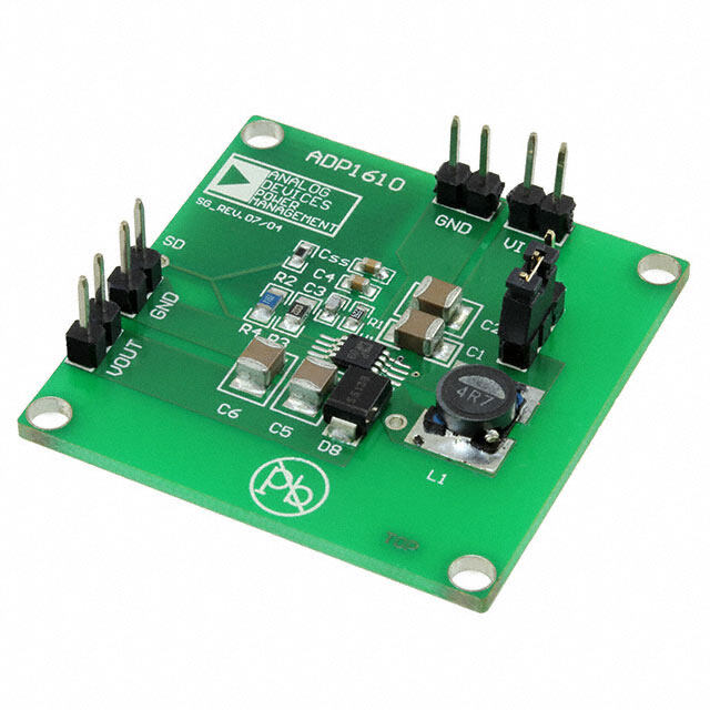
ICGOO电子元器件商城为您提供TPS61020EVM-025由Texas Instruments设计生产,在icgoo商城现货销售,并且可以通过原厂、代理商等渠道进行代购。 TPS61020EVM-025价格参考。Texas InstrumentsTPS61020EVM-025封装/规格:评估板 - DC/DC 与 AC/DC(离线)SMPS, TPS61020 - DC/DC, Step Up 1, Non-Isolated Outputs Evaluation Board。您可以下载TPS61020EVM-025参考资料、Datasheet数据手册功能说明书,资料中有TPS61020EVM-025 详细功能的应用电路图电压和使用方法及教程。
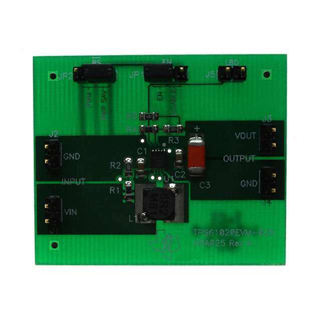
TPS61020EVM-025是德州仪器(Texas Instruments)推出的一款评估板,用于评估TPS61020升压转换器的性能。该评估板属于DC/DC与AC/DC(离线)开关电源(SMPS)评估板分类,主要用于开发和测试基于TPS61020的电源解决方案。

该评估板的主要应用场景包括:

1. 便携式电子设备开发:适用于测试TPS61020在低输入电压条件下(如单节电池供电)的升压性能,常见于手机、平板、穿戴设备等便携设备中的电源管理应用。

2. 电源管理系统评估:工程师可利用该评估板快速验证TPS61020在不同负载和输入电压下的效率、稳定性与热性能,便于优化电源设计。

3. LED驱动测试:TPS61020适用于驱动LED,因此该评估板可用于LED照明系统开发,评估其在恒流输出模式下的表现。

4. 传感器与无线模块供电方案验证:在物联网(IoT)、无线通信模块等低功耗系统中,评估该升压芯片为传感器或射频模块提供稳定电压的能力。

5. 教育与研发用途:高校、实验室或研发部门用于教学演示或新型电源拓扑结构的研究与验证。

总结:TPS61020EVM-025适用于便携设备、LED驱动、传感器供电等领域的电源设计评估,帮助工程师快速实现TPS61020在实际应用中的性能验证与优化。
| 参数 | 数值 |
| 产品目录 | 编程器,开发系统半导体 |
| 描述 | EVAL MODULE FOR TPS61020-025电源管理IC开发工具 TPS61020 Eval Mod |
| 产品分类 | |
| 品牌 | Texas Instruments |
| 产品手册 | http://www.ti.com/lit/pdf/slvu100 |
| 产品图片 |
|
| rohs | 否含铅 / 不受限制有害物质指令(RoHS)规范要求限制 |
| 产品系列 | 电源管理IC开发工具,Texas Instruments TPS61020EVM-025- |
| 数据手册 | 点击此处下载产品Datasheethttp://www.ti.com/lit/pdf/slvu100 |
| 产品型号 | TPS61020EVM-025 |
| 主要用途 | DC/DC,步升 |
| 产品 | Evaluation Boards |
| 产品目录页面 | |
| 产品种类 | 电源管理IC开发工具 |
| 使用的IC/零件 | TPS61020 |
| 其它名称 | 296-18969 |
| 制造商产品页 | http://www.ti.com/general/docs/suppproductinfo.tsp?distId=10&orderablePartNumber=TPS61020EVM-025 |
| 功率-输出 | - |
| 参考设计库 | http://www.digikey.com/rdl/4294959904/4294959903/85 |
| 商标 | Texas Instruments |
| 尺寸 | 45.7 mm x 38.1 mm |
| 工具用于评估 | TPS61020 |
| 工厂包装数量 | 1 |
| 所含物品 | 板 |
| 板类型 | 完全填充 |
| 标准包装 | 1 |
| 电压-输入 | 0.9 V ~ 6.5 V |
| 电压-输出 | 3.3V |
| 电流-输出 | 1.5A |
| 相关产品 | /product-detail/zh/TPS61020DRCR/296-15752-1-ND/593893/product-detail/zh/TPS61020DRCR/296-15752-2-ND/593898/product-detail/zh/TPS61020DRCR/296-15752-6-ND/748202/product-detail/zh/TPS61020DRCRG4/TPS61020DRCRG4-ND/1672113 |
| 稳压器拓扑 | 升压 |
| 类型 | Voltage Regulators - Switching Regulators |
| 输入电压 | 0.9 V to 6 V |
| 输出和类型 | 1,非隔离 |
| 输出电压 | 1.8 V to 5.5 V |
| 频率-开关 | - |


- 商务部:美国ITC正式对集成电路等产品启动337调查
- 曝三星4nm工艺存在良率问题 高通将骁龙8 Gen1或转产台积电
- 太阳诱电将投资9.5亿元在常州建新厂生产MLCC 预计2023年完工
- 英特尔发布欧洲新工厂建设计划 深化IDM 2.0 战略
- 台积电先进制程称霸业界 有大客户加持明年业绩稳了
- 达到5530亿美元!SIA预计今年全球半导体销售额将创下新高
- 英特尔拟将自动驾驶子公司Mobileye上市 估值或超500亿美元
- 三星加码芯片和SET,合并消费电子和移动部门,撤换高东真等 CEO
- 三星电子宣布重大人事变动 还合并消费电子和移动部门
- 海关总署:前11个月进口集成电路产品价值2.52万亿元 增长14.8%


PDF Datasheet 数据手册内容提取
(cid:1)(cid:2)(cid:3)(cid:4)(cid:5)(cid:6)(cid:7)(cid:6)(cid:8)(cid:9)(cid:10) (cid:11)(cid:12)(cid:13)(cid:14)(cid:15)(cid:8)(cid:16)(cid:16)(cid:12)(cid:17)(cid:12)(cid:18)(cid:19)(cid:17)(cid:20) (cid:3)(cid:20)(cid:19)(cid:17)(cid:14)(cid:21)(cid:22)(cid:19)(cid:22)(cid:23)(cid:24) (cid:25)(cid:22)(cid:22)(cid:24)(cid:26) (cid:27)(cid:22)(cid:19)(cid:28)(cid:18)(cid:21)(cid:26)(cid:18)(cid:21)(cid:24) User’s Guide November 2003 Power Management Products SLVU100
IMPORTANT NOTICE Texas Instruments Incorporated and its subsidiaries (TI) reserve the right to make corrections, modifications, enhancements, improvements, and other changes to its products and services at any time and to discontinue any product or service without notice. Customers should obtain the latest relevant information before placing orders and should verify that such information is current and complete. All products are sold subject to TI’s terms and conditions of sale supplied at the time of order acknowledgment. TI warrants performance of its hardware products to the specifications applicable at the time of sale in accordance with TI’s standard warranty. Testing and other quality control techniques are used to the extent TI deems necessary to support this warranty. Except where mandated by government requirements, testing of all parameters of each product is not necessarily performed. TI assumes no liability for applications assistance or customer product design. Customers are responsible for their products and applications using TI components. To minimize the risks associated with customer products and applications, customers should provide adequate design and operating safeguards. TI does not warrant or represent that any license, either express or implied, is granted under any TI patent right, copyright, mask work right, or other TI intellectual property right relating to any combination, machine, or process in which TI products or services are used. Information published by TI regarding third−party products or services does not constitute a license from TI to use such products or services or a warranty or endorsement thereof. Use of such information may require a license from a third party under the patents or other intellectual property of the third party, or a license from TI under the patents or other intellectual property of TI. Reproduction of information in TI data books or data sheets is permissible only if reproduction is without alteration and is accompanied by all associated warranties, conditions, limitations, and notices. Reproduction of this information with alteration is an unfair and deceptive business practice. TI is not responsible or liable for such altered documentation. Resale of TI products or services with statements different from or beyond the parameters stated by TI for that product or service voids all express and any implied warranties for the associated TI product or service and is an unfair and deceptive business practice. TI is not responsible or liable for any such statements. Following are URLs where you can obtain information on other Texas Instruments products & application solutions: Products Applications Amplifiers amplifier.ti.com Audio www.ti.com/audio Data Converters dataconverter.ti.com Automotive www.ti.com/automotive DSP dsp.ti.com Broadband www.ti.com/broadband Interface interface.ti.com Digital Control www.ti.com/digitalcontrol Logic logic.ti.com Military www.ti.com/military Power Mgmt power.ti.com Optical Networking www.ti.com/opticalnetwork Microcontrollers microcontroller.ti.com Secruity www.ti.com/security Telephony www.ti.com/telephony Video & Imaging www.ti.com/video Wireless www.ti.com/wireless Mailing Address: Texas Instruments Post Office Box 655303 Dallas, Texas 75265 Copyright 2003, Texas Instruments Incorporated
EVM IMPORTANT NOTICE Texas Instruments (TI) provides the enclosed product(s) under the following conditions: This evaluation kit being sold by TI is intended for use for ENGINEERING DEVELOPMENT OR EVALUATION PURPOSES ONLY and is not considered by TI to be fit for commercial use. As such, the goods being provided may not be complete in terms of required design-, marketing-, and/or manufacturing-related protective considerations, including product safety measures typically found in the end product incorporating the goods. As a prototype, this product does not fall within the scope of the European Union directive on electromagnetic compatibility and therefore may not meet the technical requirements of the directive. Should this evaluation kit not meet the specifications indicated in the EVM User’s Guide, the kit may be returned within 30 days from the date of delivery for a full refund. THE FOREGOING WARRANTY IS THE EXCLUSIVE WARRANTY MADE BY SELLER TO BUYER AND IS IN LIEU OF ALL OTHER WARRANTIES, EXPRESSED, IMPLIED, OR STATUTORY, INCLUDING ANY WARRANTY OF MERCHANTABILITY OR FITNESS FOR ANY PARTICULAR PURPOSE. The user assumes all responsibility and liability for proper and safe handling of the goods. Further, the user indemnifies TI from all claims arising from the handling or use of the goods. Please be aware that the products received may not be regulatory compliant or agency certified (FCC, UL, CE, etc.). Due to the open construction of the product, it is the user’s responsibility to take any and all appropriate precautions with regard to electrostatic discharge. EXCEPT TO THE EXTENT OF THE INDEMNITY SET FORTH ABOVE, NEITHER PARTY SHALL BE LIABLE TO THE OTHER FOR ANY INDIRECT, SPECIAL, INCIDENTAL, OR CONSEQUENTIAL DAMAGES. TI currently deals with a variety of customers for products, and therefore our arrangement with the user is not exclusive. TI assumes no liability for applications assistance, customer product design, software performance, or infringement of patents or services described herein. Please read the EVM User’s Guide and, specifically, the EVM Warnings and Restrictions notice in the EVM User’s Guide prior to handling the product. This notice contains important safety information about temperatures and voltages. For further safety concerns, please contact the TI application engineer. Persons handling the product must have electronics training and observe good laboratory practice standards. No license is granted under any patent right or other intellectual property right of TI covering or relating to any machine, process, or combination in which such TI products or services might be or are used. Mailing Address: Texas Instruments Post Office Box 655303 Dallas, Texas 75265 Copyright 2003, Texas Instruments Incorporated
EVM WARNINGS AND RESTRICTIONS It is important to operate this EVM within the input voltage range of 0.9 V to 6 V and output voltage range of 1.8 V to 5.5 V. Exceeding the specified input range may cause unexpected operation and/or irreversible damage to the EVM. If there are questions concerning the input range, please contact a TI field representative prior to connecting the input power. Applying loads outside of the specified output range may result in unintended operation and/or possible permanent damage to the EVM. Please consult the EVM User’s Guide prior to connecting any load to the EVM output. If there is uncertainty as to the load specification, please contact a TI field representative. During normal operation, some circuit components may have case temperatures greater than 60°C. The EVM is designed to operate properly with certain components above 60°C as long as the input and output ranges are maintained. These components include but are not limited to linear regulators, switching transistors, pass transistors, and current sense resistors. These types of devices can be identified using the EVM schematic located in the EVM User’s Guide. When placing measurement probes near these devices during operation, please be aware that these devices may be very warm to the touch. Mailing Address: Texas Instruments Post Office Box 655303 Dallas, Texas 75265 Copyright 2003, Texas Instruments Incorporated
Related Documentation From Texas Instruments Preface (cid:1)(cid:2)(cid:3)(cid:4)(cid:5)(cid:6)(cid:7)(cid:8)(cid:9)(cid:5)(cid:10)(cid:8)(cid:11)(cid:9)(cid:12) About This Manual This user’s guide describes the operation of the TPS61020EVM low-power, dc−dc evaluation module (EVM) for a high-efficiency, boost converter. The guide includes setup instructions for the hardware, a schematic diagram, a bill of materials (BOM), and PCB layout drawings for the evaluation module. How to Use This Manual This document contains the following chapters: (cid:1) Chapter 1—Introduction (cid:1) Chapter 2—Evaluation with the TPS61020EVM (cid:1) Chapter 3—Schematic, BOM, and PCB layout Related Documentation From Texas Instruments TPS61020 data sheet (SLVS451) FCC Warning This equipment is intended for use in a laboratory test environment only. It gen- erates, uses, and can radiate radio frequency energy and has not been tested for compliance with the limits of computing devices pursuant to subpart J of part 15 of FCC rules, which are designed to provide reasonable protection against radio frequency interference. Operation of this equipment in other en- vironments may cause interference with radio communications, in which case the user at his own expense will be required to take whatever measures may be required to correct this interference. iii
iv
Contents (cid:13)(cid:14)(cid:15)(cid:12)(cid:2)(cid:15)(cid:12)(cid:9) 1 Introduction . . . . . . . . . . . . . . . . . . . . . . . . . . . . . . . . . . . . . . . . . . . . . . . . . . . . . . . . . . . . . . . . . . . . . 1-1 1.1 EVM Ordering Information . . . . . . . . . . . . . . . . . . . . . . . . . . . . . . . . . . . . . . . . . . . . . . . . . . . 1-2 2 Evaluation With the TPS61020EVM . . . . . . . . . . . . . . . . . . . . . . . . . . . . . . . . . . . . . . . . . . . . . . . 2-1 2.1 Maximum Output Current . . . . . . . . . . . . . . . . . . . . . . . . . . . . . . . . . . . . . . . . . . . . . . . . . . . . 2-2 2.2 Enable (EN) Jumper . . . . . . . . . . . . . . . . . . . . . . . . . . . . . . . . . . . . . . . . . . . . . . . . . . . . . . . . 2-2 2.3 Mode Selection Jumper (PS) . . . . . . . . . . . . . . . . . . . . . . . . . . . . . . . . . . . . . . . . . . . . . . . . . 2-2 2.4 Efficiency of TPS61020EVM . . . . . . . . . . . . . . . . . . . . . . . . . . . . . . . . . . . . . . . . . . . . . . . . . 2-3 3 Schematic, BOM, and PCB Layout . . . . . . . . . . . . . . . . . . . . . . . . . . . . . . . . . . . . . . . . . . . . . . . . 3-1 3.1 HPA025 EVM Schematic . . . . . . . . . . . . . . . . . . . . . . . . . . . . . . . . . . . . . . . . . . . . . . . . . . . . 3-2 3.2 Bill of Materials . . . . . . . . . . . . . . . . . . . . . . . . . . . . . . . . . . . . . . . . . . . . . . . . . . . . . . . . . . . . . 3-2 3.3 PCB Layout of the TPS61020EVM . . . . . . . . . . . . . . . . . . . . . . . . . . . . . . . . . . . . . . . . . . . . 3-3 (cid:10)(cid:8)(cid:16)(cid:17)(cid:11)(cid:2)(cid:9) 2−1 Maximum Output Current vs Input Voltage. . . . . . . . . . . . . . . . . . . . . . . . . . . . . . . . . . . . . . . . 2-2 2−2 Efficiency for 3.3 VOUT . . . . . . . . . . . . . . . . . . . . . . . . . . . . . . . . . . . . . . . . . . . . . . . . . . . . . . . . 2-3 3−1 TPS61020EVM (HPA025) Schematic . . . . . . . . . . . . . . . . . . . . . . . . . . . . . . . . . . . . . . . . . . . . 3-2 3−2 Component Placement . . . . . . . . . . . . . . . . . . . . . . . . . . . . . . . . . . . . . . . . . . . . . . . . . . . . . . . . 3-3 3−3 Top Layer . . . . . . . . . . . . . . . . . . . . . . . . . . . . . . . . . . . . . . . . . . . . . . . . . . . . . . . . . . . . . . . . . . . . 3-3 3−4 Bottom Layer . . . . . . . . . . . . . . . . . . . . . . . . . . . . . . . . . . . . . . . . . . . . . . . . . . . . . . . . . . . . . . . . . 3-3 (cid:6)(cid:3)(cid:18)(cid:19)(cid:2)(cid:9) 1−1 EVM Ordering Information. . . . . . . . . . . . . . . . . . . . . . . . . . . . . . . . . . . . . . . . . . . . . . . . . . . . . . 1-2 3−1 TPS61020EVM (HPA025) Bill of Materials . . . . . . . . . . . . . . . . . . . . . . . . . . . . . . . . . . . . . . . . 3-2 v
Contents vi
Chapter 1 (cid:20)(cid:15)(cid:12)(cid:11)(cid:14)(cid:4)(cid:17)(cid:21)(cid:12)(cid:8)(cid:14)(cid:15) The Texas Instruments TPS61020 evaluation module (EVM) for low-power, high-efficiency, boost converter helps designers evaluate the TPS61020 device. The EVM makes it possible to evaluate different device modes as well as the device performance. The TPS61020EVM is set to 3.3 V. The TPS61020EVM can be easily set up to provide any output voltage between 1.8 V and 5.5 V by adjusting the external resistor divider. Refer to the datasheet (SLVS451) for the output voltage calculation. The TPS61020 has an input voltage range between 0.9 V and 6.5V. Topic Page 1.1 EVM Ordering Information . . . . . . . . . . . . . . . . . . . . . . . . . . . . . . . . . . . . . 1-2 Introduction 1-1
EVM Ordering Information 1.1 EVM Ordering Information Table 1−1.EVM Ordering Information EVM Number Description TPS61020EVM-025 Adjustable output voltage version set to 3.3 V. 1-2
Chapter 2 (cid:22)(cid:23)(cid:3)(cid:19)(cid:17)(cid:3)(cid:12)(cid:8)(cid:14)(cid:15) (cid:24)(cid:8)(cid:12)(cid:7) (cid:12)(cid:7)(cid:2) (cid:6)(cid:25)(cid:26)(cid:27)(cid:28)(cid:29)(cid:30)(cid:29)(cid:22)(cid:31)! This chapter details the evaluation process and features of the EVM. For this purpose, a load is connected to the output pins Vout and GND, allowing the load current to be adjusted between 0 A and the maximum current shown in Figure 2−1. For accurate output voltage and input voltage measurements, it is important to measure the voltage on the input and output voltage terminals with a voltmeter connected directly to the input voltage or output voltage terminals. This eliminates any measurement errors related to voltage drops along the input and output terminal wires connected to the power supply or load. Topic Page 2.1 Maximum Output Current . . . . . . . . . . . . . . . . . . . . . . . . . . . . . . . . . . . . . . 2-2 2.2 Enable (EN) Jumper . . . . . . . . . . . . . . . . . . . . . . . . . . . . . . . . . . . . . . . . . . . 2-2 2.3 Mode Selection Jumper (PS) . . . . . . . . . . . . . . . . . . . . . . . . . . . . . . . . . . . 2-2 2.4 Efficiency of TPW61020EVM . . . . . . . . . . . . . . . . . . . . . . . . . . . . . . . . . . . 2-3 Evaluation With the TPS61020EVM 2-1
Maximum Output Current 2.1 Maximum Output Current Figure 2−1.Maximum Output Current vs Input Voltage 1400 1200 mA VO = 3.3 V VO = 5 V − 1000 nt e r r Cu 800 ut p ut O 600 m u m 400 VO = 1.8 V xi a M 200 0 0.9 1.7 2.5 3.3 4.1 4.9 5.7 6.5 VI − Input Voltage − V 2.2 Enable (EN) Jumper This jumper is used to enable the device. Connecting the EN pin to ENABLE enables the part. Connecting the EN pin to DISABLE disables the device. 2.3 Mode Selection Jumper (PS) This jumper is used to choose between PWM and PWR SAV modes of operation. Setting the jumper across PWM forces the device into the low noise fixed frequency pulse width modulation (PWM) mode. Setting the jumper across PWR SAV enables the power save mode where the device enters a pulse frequency modulation mode (PFM) at light to medium load currents, which reduces quiescent current and switching frequency to a minimum to achieve highest efficiency over the entire load current range. 2-2
Efficiency of TPS61020EVM 2.4 Efficiency of TPS61020EVM Figure 2−2.Efficiency for 3.3 V OUT 100 95 2.4 VI 90 1.8 VI 85 y 80 c n e ci 75 Effi 0.9 VI 70 65 60 55 50 10 100 200 300 400 500 600 700 800 900 IL − Load Current − mA Physically smaller inductors can be used to save board space, or reduce height at the expense of lower efficiency. Conversely, physically larger induc- tors give better efficiency. Evaluation With the TPS61020EVM 2-3
2-4
Chapter 3 (cid:26)(cid:21)(cid:7)(cid:2)"(cid:3)(cid:12)(cid:8)(cid:21)# $%!# (cid:3)(cid:15)(cid:4) (cid:25)(cid:13)$ &(cid:3)’(cid:14)(cid:17)(cid:12) This chapter includes the schematic shown in Figure 3−1, bill of materials table, and layout for the EVM. Topic Page 3.1 HPA025 EVM Schematic . . . . . . . . . . . . . . . . . . . . . . . . . . . . . . . . . . . . . . . 3-2 3.2 Bill of Materials . . . . . . . . . . . . . . . . . . . . . . . . . . . . . . . . . . . . . . . . . . . . . . . 3-2 3.3 PCB Layout of the TPS61020EVM . . . . . . . . . . . . . . . . . . . . . . . . . . . . . . 3-3 Schematic, BOM, and PCB Layout 3-1
HPA025 EVM Schematic 3.1 HPA025 EVM Schematic Figure 3−1 shows the HPA025 EVM schematic diagram. The bill of materials for the TPS61020EVM is shown in Table 3−1. More details about the design and component selection for the dc-dc converter can be found in the data sheet. Figure 3−1.TPS61020EVM (HPA025) Schematic U1 TPS61020DRC L1 0.9 − 6.5 V VIN J1 12 6.2 µH 187609VPSPLBBGWSIANTD GVLBENoFuONBDt 12345 R1 3MΩ C2.22 µF+ C473 µF 12J3 VOUT J2 1 C101 µF R0 1Ω PwPd R4 R1 5MΩ GND 2 178 kΩ J5 1 JP1 R2 2 LBO EN 1 M Ω DISABLE J4 1 2 GND JP2 PWM PS PER SAV 3.2 Bill of Materials Table 3−1.TPS61020EVM (HPA025)Bill of Materials Count Ref Des Description Size MFR Part Number 1 C1 Capacitor, ceramic, 10 µF, 10 V, X5R, ±10% 805 Murata GRM21BR61A106KE19L 1 C2 Capacitor, ceramic, 2.2 µF, 16−V, X5R, ±10% 805 TDK C2012X5R1C225KT 1 C3 Capacitor, tantalum, 47 µF, 16 V, 110 mΩ, 20% 6032 (C) Vishay 594D476X0016C2T 5 J1−J5 Header, 2 pin, 100 mil spacing, (36-pin strip) 0.100 x 2 Sullins PTC36SAAN 2 JP1, JP2 Header, 3-pin, 100 mil spacing, (36-pin strip) 0.100 x 3 Sullins PTC36SAAN 1 L1 Inductor, SM Toroid, 6.2 µH, 1.8 A, 43 mΩ 74480 Sumida CDRH5D28−6R2 1 R1 Resistor, Chip, 0 Ω, 1/10 W, 1% 805 Std Std 3 R2, R3, Resistor, Chip, 1.00 MΩ, 1/10 W, 1% 805 Std Std R5 1 R4 Resistor, Chip, 178 kΩ, 1/10 W, 1% 805 Std Std 1 U1 IC, synchronous boost converter, adjustable DRC10 TI TPS61020DRC voltage 1 — PCB, 1.8 In x 1.5 In x 0.062 In Any HPA025 2 — Shunt, 100 mil, black 0.100 3M 929950−00 3-2
PCB Layout of the TPS61020EVM 3.3 PCB Layout of the TPS61020EVM The figures below show the layout for the EVM. Figure 3−2.Component Placement Figure 3−3.Top Layer Figure 3−4.Bottom Layer Schematic, BOM, and PCB Layout 3-3
3-4