ICGOO在线商城 > TPS60231RGTR
 Datasheet下载
- 型号: TPS60231RGTR
- 制造商: Texas Instruments
- 库位|库存: xxxx|xxxx
- 要求:
| 数量阶梯 | 香港交货 | 国内含税 |
| +xxxx | $xxxx | ¥xxxx |
查看当月历史价格
查看今年历史价格
TPS60231RGTR产品简介:
ICGOO电子元器件商城为您提供TPS60231RGTR由Texas Instruments设计生产,在icgoo商城现货销售,并且可以通过原厂、代理商等渠道进行代购。 提供TPS60231RGTR价格参考以及Texas InstrumentsTPS60231RGTR封装/规格参数等产品信息。 你可以下载TPS60231RGTR参考资料、Datasheet数据手册功能说明书, 资料中有TPS60231RGTR详细功能的应用电路图电压和使用方法及教程。
| 参数 | 数值 |
| 产品目录 | 集成电路 (IC)半导体 |
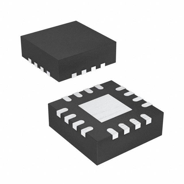
| 描述 | IC LED DRIVR WHITE BCKLGT 16-QFN稳压器—开关式稳压器 3-Ch 75-mA Charge Pump |
| DevelopmentKit | TPS60231EVM-047 |
| 产品分类 | |
| 品牌 | Texas Instruments |
| 产品手册 | http://www.ti.com/litv/slvs544a |
| 产品图片 |
|
| rohs | 符合RoHS无铅 / 符合限制有害物质指令(RoHS)规范要求 |
| 产品系列 | 电源管理 IC,稳压器—开关式稳压器,Texas Instruments TPS60231RGTR- |
| 数据手册 | |
| 产品型号 | TPS60231RGTR |
| 产品目录页面 | |
| 产品种类 | 稳压器—开关式稳压器 |
| 供应商器件封装 | 16-QFN(3x3) |
| 关闭 | Shutdown |
| 其它名称 | 296-17490-1 |
| 内部驱动器 | 是 |
| 包装 | 剪切带 (CT) |
| 单位重量 | 23 mg |
| 商标 | Texas Instruments |
| 安装类型 | 表面贴装 |
| 安装风格 | SMD/SMT |
| 封装 | Reel |
| 封装/外壳 | 16-VFQFN 裸露焊盘 |
| 封装/箱体 | VQFN-16 |
| 工作温度 | -40°C ~ 85°C |
| 工作温度范围 | - 40 C to + 85 C |
| 工厂包装数量 | 3000 |
| 开关频率 | 1 MHz |
| 恒压 | - |
| 恒流 | 是 |
| 拓扑 | PWM,切换式电容器(充电泵) |
| 拓扑结构 | Boost |
| 最大工作温度 | + 85 C |
| 最大输入电压 | 6.5 V |
| 最小工作温度 | - 40 C |
| 最小输入电压 | 2.7 V |
| 标准包装 | 1 |
| 电压-电源 | 2.7 V ~ 6.5 V |
| 电压-输出 | 5.5V |
| 电源电压-最小 | 2.7 V |
| 电源电流 | 200 uA |
| 类型 | Charge Pump |
| 类型-初级 | 背光 |
| 类型-次级 | 白色 LED |
| 系列 | TPS60231 |
| 输入电压 | 2.7 V to 6.5 V |
| 输出数 | 3 |
| 输出电压 | 5.5 V |
| 输出电流 | 75 mA |
| 输出端数量 | 1 Output |
| 配用 | /product-detail/zh/TPS60231EVM-047/296-17608-ND/705732 |
| 频率 | 750kHz ~ 1.25MHz |


.jpg)


- 商务部:美国ITC正式对集成电路等产品启动337调查
- 曝三星4nm工艺存在良率问题 高通将骁龙8 Gen1或转产台积电
- 太阳诱电将投资9.5亿元在常州建新厂生产MLCC 预计2023年完工
- 英特尔发布欧洲新工厂建设计划 深化IDM 2.0 战略
- 台积电先进制程称霸业界 有大客户加持明年业绩稳了
- 达到5530亿美元!SIA预计今年全球半导体销售额将创下新高
- 英特尔拟将自动驾驶子公司Mobileye上市 估值或超500亿美元
- 三星加码芯片和SET,合并消费电子和移动部门,撤换高东真等 CEO
- 三星电子宣布重大人事变动 还合并消费电子和移动部门
- 海关总署:前11个月进口集成电路产品价值2.52万亿元 增长14.8%


.jpg)

PDF Datasheet 数据手册内容提取
TPS60231 www.ti.com SLVS544A–OCTOBER2004–REVISEDFEBRUARY2010 WHITE LED CHARGE PUMP CURRENT SOURCE WITH PWM BRIGHTNESS CONTROL CheckforSamples:TPS60231 FEATURES 1 DESCRIPTION • RegulatedOutputCurrentWith0.4% Matching The TPS60231 charge pump is optimized for white • Drivesupto3LEDsat25mAEach LED supplies in color display backlight applications. The device provides a constant current for each LED, • LEDBrightnessControlThroughPWM which the initial value can be set by an external ControlSignal resistor. The supply voltage ranges from 2.7 V to • HighEfficiencybyFractionalConversion 6.5V and is ideally suited for all applications powered With1xand1.5xModes by a single LI-Ion battery cell or three to four NiCd, • 1MHzSwitchingFrequency NiMH, or alkaline battery cells. Over an input voltage range from 3.1 V to 6.5 V, the device provides a high • 2.7Vto6.5VOperatingInputVoltageRange output current of up to 25 mA per LED with a total of • InternalSoftstartLimitsInrushCurrent 75 mA. High efficiency is achieved by utilizing a • LowInputRippleandLowEMI 1x/1.5x fractional conversion technique in combination with very low dropout current sources. In • OvercurrentandOvertemperatureProtected addition, the current controlled charge pump ensures • UndervoltageLockoutWithHysteresis low input current ripple and EMI. Only two external • Ultra-Small3mmx3mmQFNPackage 1µF and two 0.47 µF capacitors are required to build a complete small and low cost power supply solution. APPLICATIONS To reduce board space to a minimum, the device switches at 1 MHz operating frequency and is • WhiteLEDBacklightforColorDisplaysin availableinasmall16-pinQFN(RGT)package. CellularPhones,SmartPhones,PDAs, HandheldPCs,DigitalCameras,and SPACER Camcorders • KeypadBacklight VIN VOUT 1 (cid:1)F VINt o= 26..75 VV 0.47 (cid:1)F C1+ D1 D2 C1− D3 C2+ 0.47 (cid:1)F C2− 1 (cid:1)F EN1 EN2 ISET GND PGND 1 Pleasebeawarethatanimportantnoticeconcerningavailability,standardwarranty,anduseincriticalapplicationsofTexas Instrumentssemiconductorproductsanddisclaimerstheretoappearsattheendofthisdatasheet. PRODUCTIONDATAinformationiscurrentasofpublicationdate. Copyright©2004–2010,TexasInstrumentsIncorporated Products conform to specifications per the terms of the Texas Instruments standard warranty. Production processing does not necessarilyincludetestingofallparameters.
TPS60231 SLVS544A–OCTOBER2004–REVISEDFEBRUARY2010 www.ti.com This integrated circuit can be damaged by ESD. Texas Instruments recommends that all integrated circuits be handled with appropriateprecautions.Failuretoobserveproperhandlingandinstallationprocedurescancausedamage. ESDdamagecanrangefromsubtleperformancedegradationtocompletedevicefailure.Precisionintegratedcircuitsmaybemore susceptibletodamagebecauseverysmallparametricchangescouldcausethedevicenottomeetitspublishedspecifications. ORDERINGINFORMATION PACKAGEDDEVICE(1) (2) PACKAGE MARKING TPS60231RGTR QFN BKH (1) Tindicatesshipmentintapeandreelonaminireelwith250unitsperreel. (2) Rindicatesshipmentintapeandreelwith3000unitsperreel. ABSOLUTE MAXIMUM RATINGS overoperatingfree-airtemperaturerange(unlessotherwisenoted)(1) UNIT V Supplyvoltage –0.3Vto7V I VoltageatEN1,EN2,VOUT,ISET –0.3VtoV I OutputcurrentatVOUT 150mA T Maximumjunctiontemperature 150°C J T Operatingfree-airtemperature –40°Cto85°C A T Storagetemperature –65°Cto150°C st (1) Stressesbeyondthoselistedunder"absolutemaximumratings"maycausepermanentdamagetothedevice.Thesearestressratings only,andfunctionaloperationofthedeviceattheseoranyotherconditionsbeyondthoseindicatedunder"recommendedoperating conditions"isnotimplied.Exposuretoabsolute-maximum-ratedconditionsforextendedperiodsmayaffectdevicereliability. DISSIPATION RATINGS(1) T ≤25°C DERATINGFACTOR T =70°C T =85°C PACKAGE A A A POWERRATING ABOVET =25°C POWERRATING POWERRATING A 16-PinQFN(RGT) 1.9W 20mW/°C 1W 760mW (1) ThethermalresistancejunctiontoambientoftheQFNpackageis52°C/W. RECOMMENDED OPERATING CONDITIONS MIN TYP MAX UNIT SupplyvoltageatVIN 2.7 6.5 V MaximumoutputcurrentatVOUT 75 mA C Inputcapacitor 1 µF I C Outputcapacitor 0.47 1 µF o Flyingcapacitor,C1,C2 0.22 0.47 µF Operatingjunctiontemperature -40 125 °C 2 SubmitDocumentationFeedback Copyright©2004–2010,TexasInstrumentsIncorporated ProductFolderLink(s):TPS60231
TPS60231 www.ti.com SLVS544A–OCTOBER2004–REVISEDFEBRUARY2010 ELECTRICAL CHARACTERISTICS V =3.6V,EN1=EN2=V,T =-40°Cto85°C(unlessotherwisenoted) I I A PARAMETER TESTCONDITIONS MIN TYP MAX UNIT SUPPLYVOLTAGEANDCURRENT I =0mAto75mA 2.7 6.5 V O V Inputvoltagerange I I =0mAto45mA,VLED≤2.1V,T=0°Cto85°C 2.5 6.5 V O V =4.2V,x1-mode,EN1=EN2=1,ISET=20µA 200 µA I I Operatingquiescentcurrent Q I =0mA,x1.5-mode 2.1 mA O I Shutdowncurrent EN2=EN1=GND 0.1 1 µA SD CHARGEPUMPSTAGE V Overvoltagelimit LED1unconnected,V =4.2V 5.5 V OUT I Startuptime C =1µF,I ≥0.9I ,set 375 µs O DX DX Softstartduration 160 µs f Switchingfrequency 0.75 1 1.25 MHz h Efficiency V =3.7V,I =15mAeach,V =3.1V 83% I LED DX Shutdowntemperature Temperaturerising 160 °C Shutdowntemperaturehysteresis 20 °C Inputcurrentlimit EN2=EN1=1,ISET=100µA 350 mA CURRENTSINKS Recommendedmaximumcurrentper 3.2V≤V ≤6.5V I I 25 mA Dx currentsink CurrentintoeachcurrentsinkwhenISET I 3.0V≤V ≤6.5V,ISETshortedtoGND 50 mA Dx isshortedtoGND I Currentmatchingbetweenanytwooutputs V =3.1V,T =25°C –2% 0.4% 2% Dx A 3.2V≤V ≤6.5V,V =3.1V,EN1=EN2=1, Lineregulation I Dx ±3% ISET=80µA EN2=0,EN1=1 200 V Referencevoltageforcurrentset EN2=1,EN1=0 400 mV ISET EN2=1,EN1=1 580 600 620 Iset RecommendedISETpincurrentrange 4 130 µA K I toISETcurrentratio EN2=EN1=1,ISET=80µA 230 260 280 Dx EN2=0,EN1=1 200 V VoltageatDxtoGND EN2=1,EN1=0 300 mV source EN2=1,EN1=1 400 ENABLE1,ENABLE2 V EN1,EN2highlevelinputvoltage 1.3 V IH V EN1,EN2lowlevelinputvoltage 0.3 V IL EN1,EN2trippointhysteresis 50 mV I EN2inputleakagecurrent EN1,EN2=GNDorEN2=V,V =6.5V 0.01 1 µA IKG I I I EN1inputleakagecurrent EN1=V,V =4.2V 11 15 µA IKG I I UVLO Undervoltagelockoutthreshold Inputvoltagefalling 2.1 V Undervoltagelockouthysteresis 50 mV FrequencyrangeatPWM 0 50 kHz RecommendedON-timeforPWMsignal 2.5 µs DelaytimewhenEN1=EN2gotoGNDafterwhich Shutdowndelaytime 0.5 0.85 1.5 ms theTPS60231shutsdowncompletely Copyright©2004–2010,TexasInstrumentsIncorporated SubmitDocumentationFeedback 3 ProductFolderLink(s):TPS60231
TPS60231 SLVS544A–OCTOBER2004–REVISEDFEBRUARY2010 www.ti.com PIN ASSIGNMENT QFN PACKAGE (TOP VIEW) − − + + 2 1 1 2 C C C C 12 11 10 9 13 VIN VOUT 8 14 GND PGND 7 15 EN1 D1 6 16 EN2 D2 5 1 2 3 4 T C C 3 E N N D S I PinFunctions PIN I/O DESCRIPTION NAME NO. C1+ 10 – ConnecttotheflyingcapacitorC1 C1– 11 – ConnecttotheflyingcapacitorC1 C2+ 9 – ConnecttotheflyingcapacitorC2 C2– 12 – ConnecttotheflyingcapacitorC2 D1-D3 6-4 I Currentsinkinput.ConnectthecathodeofthewhiteLEDstotheseinputs. Enableinput.Alogichighenablestheconverter,logiclowforcesthedeviceintoshutdownmodereducing EN1 15 I thesupplycurrenttolessthan1µAifEN2istiedtoGND. AnappliedPWMsignalreducestheLEDcurrentasafunctionofthedutycycleofthePWMsignal.EN1and EN2canbetiedtogetherforPWMdimmingbetween0mAandthemaximumsetwithISET.EN1andEN2 EN2 16 I canalsobeusedfordigitaldimmingwith4stepsfrom0mAtothemaximumcurrentsetwithISET.Seethe applicationsectionformoredetails. GND 14 – Analogground ISET 1 I ConnectaresistorbetweenthispinandGNDtosetthemaximumcurrentthroughtheLEDs. NC 2,3 – Nointernalconnection PGND 7 – Powerground VIN 13 I Supplyvoltageinput VOUT 8 0 ConnecttheoutputcapacitorandtheanodeoftheLEDstothispin. PowerPAD – – ConnectwithPGNDandGND 4 SubmitDocumentationFeedback Copyright©2004–2010,TexasInstrumentsIncorporated ProductFolderLink(s):TPS60231
TPS60231 www.ti.com SLVS544A–OCTOBER2004–REVISEDFEBRUARY2010 FUNCTIONALBLOCKDIAGRAM 1 (cid:1)F VOUT C1+ 0.47 (cid:1)F C1− Current D3 Sinks C2+ Charge D2 Pump 0.47 (cid:1)F D1 C2− VIN 1 (cid:1)F Reference Control ISET EN1 EN2 RSET PGND GND SPACER TYPICAL CHARACTERISTICS Table of Graphs FIGURE vsInputvoltage(I =25mA,15mA,10mA,5mAperLED), LED 1 EN2=0,EN1=1 vsInputvoltage(I =25mA,15mA,10mA,5mAperLED), h Efficiency LED 2 EN2=1,EN1=0 vsInputvoltage(I =25mA,15mA,10mA,5mAperLED), LED 3 EN2=EN1=1 I Quiescentcurrent vsInputvoltage(T =–40°C,25°C,85°C)(measuredwithI =5mA) 4 Q A D1 Maximumoutputcurrentfromchargepump vsInputvoltage(T =–40°C,25°C,85°C) 5 stage A f Switchingfrequency vsFree-AirTemperature(T =-40°Cto85°C,V =3.6V) 6 s A I vsDutycycleonPWM(I maxsetto20mA) LEDcurrent,I LED 7 LED Forf=32kHzandf=1kHz,DC=1%to100%,V =3.6V I V andI vstimeonscope,LEDcurrentatD1with Linetransientresponse I D1 8 V =4.2Vto3.6Vto4.2VwithEN2=EN1=11,3x20mA I PWMsignalandcurrentatD1vstimeonscope Dimmingresponse f=32kHzandf=1kHz,V =3.6V,dutycycle=50%, 9,10 I EN1=EN2=PWM V =3.6V,3x20mA,EN1=EN2=00changedto 11 Startuptiming I EN2=EN1=11 Copyright©2004–2010,TexasInstrumentsIncorporated SubmitDocumentationFeedback 5 ProductFolderLink(s):TPS60231
TPS60231 SLVS544A–OCTOBER2004–REVISEDFEBRUARY2010 www.ti.com EFFICIENCY EFFICIENCY vs vs INPUTVOLTAGE INPUTVOLTAGE 100 100 90 ILED = 25 mA 90 ILED = 25 mA 80 80 70 ILED = 15 mA 70 ILED = 15 mA % 60 % 60 cy − 50 ILED = 10 mA y − 50 ILED = 10 mA n c e n Effici 40 ILED = 5 mA Efficie 40 ILED = 5 mA 30 30 20 20 10 10 0 0 2.7 3.1 3.5 3.9 4.3 4.7 5.1 5.5 5.9 6.3 2.7 3.1 3.5 3.9 4.3 4.7 5.1 5.5 5.9 6.3 VI − Input Voltage − V VI − Input Voltage − V Figure1. Figure2. EFFICIENCY QUIESCENTCURRENT vs vs INPUTVOLTAGE INPUTVOLTAGE 90 3 2.8 80 ILED = 25 mA 2.6 TA = −40(cid:1)C A 70 ILED = 15 mA − m 2.4 nt 2.2 60 re 2 TA = 25(cid:1)C r u % C 1.8 ency − 4500 ILED = 5 mA ILED = 10 mA escent 11..46 TA = 85(cid:1)C Effici 30 − Qui 1.21 Q I 0.8 20 0.6 0.4 10 0.2 0 0 2.7 3.1 3.5 3.9 4.3 4.7 5.1 5.5 5.9 6.3 2.7 3.1 3.5 3.9 4.3 4.7 5.1 5.5 5.9 6.3 VI − Input Voltage − V VI − Input Voltage − V Figure3. Figure4. 6 SubmitDocumentationFeedback Copyright©2004–2010,TexasInstrumentsIncorporated ProductFolderLink(s):TPS60231
TPS60231 www.ti.com SLVS544A–OCTOBER2004–REVISEDFEBRUARY2010 MAXIMUMOUTPUTCURRENT SWITCHINGFREQUENCY vs vs INPUTVOLTAGE FREE-AIRTEMPERATURE 0.15 1040 VLED = 3 V TA = 25(cid:1)C VI = 3.6 V A VLED = 3.2 V 1030 nt − VLED = 3.4 V kHz urre 0.10 VLED = 3.6 V y − 1020 C c utput VLED = 3.8 V equen 1010 O Fr m g u n m hi axi 0.05 witc 1000 M S − O 990 I 0 980 2.7 3.1 3.5 3.9 4.3 4.7 5.1 5.5 5.9 6.3 −40−30−20−10 0 10 20 30 40 50 60 70 80 VI − Input Voltage − V TA − Free-Air Temperature − (cid:1)C Figure5. Figure6. D1LEDCURRENT vs DUTYCYCLE LINETRANSIENT 25 EN1 = 1, EN2 = 1, VI = 3.6 V to 4.2 V, VI = 3.6 V, ILED = 20 mA, 3 LEDs Connected, ILED max set to 20 mA ILED(D1) Measured With 1 (cid:1) Resistor, div TA = 25(cid:1)C A 20 V/ m m ent − 500 VI 3.6 V rr 15 u C D E L D1 10 − 1) f = 32 kHz v ILED(D1) D di AC D( A/ E 5 m IL 1 f = 1 kHz 0 0 10 20 30 40 50 60 70 80 90 100 100 (cid:2)s/div Duty Cycle − % Figure7. Figure8. Copyright©2004–2010,TexasInstrumentsIncorporated SubmitDocumentationFeedback 7 ProductFolderLink(s):TPS60231
TPS60231 SLVS544A–OCTOBER2004–REVISEDFEBRUARY2010 www.ti.com DIMMINGRESPONSE DIMMINGRESPONSE PWM PWM v 2 V/div 0 V 2 V/di 0 V PIfL =WE D3M 2= I kn2H0to zm ,E TANA,1 3= a L2n5Ed(cid:1)D CEsN C2o, nVnI e=c 3t.e6d V,, PIfL =WE D1M =k I Hn20zto, m TEAAN ,=1 3 2a L5n(cid:1)EdCD EsN C2o, nVnI e=c 3t.e6d V,, A/div ILED(D1) A/div ILED(D1) m m 10 0 A 10 0 A 200 (cid:1)s/div 5 (cid:1)s/div Figure9. Figure10. STARTUPTIMING v EN1 + EN2 di 0 V V/ 5 VO v di 0 V V/ 1 ILED v di A/ VI = 3.6 V , ILED = 20 mA, m 3 LED’s Connected, 0 A 20 TA = 25(cid:1)C 20 (cid:1)s/div Figure11. DETAILED DESCRIPTION OPERATION The TPS60231 uses a fractional conversion charge pump to generate a supply voltage for the integrated current sinks. These current sinks are used to ensure a constant current for each LED. Depending on the input voltage and programmed LED current, the charge pump either operates in the 1x mode or in the 1.5x mode. By switching automatically between these two modes, the circuit optimizes power conversion efficiency as well as extendsoperatingtimebyallowingthedischargeofthebatterycompletely. The charge pump can generate 75 mA of output current, so each of the 3 LED outputs can be powered with up to 25 mA of current. The maximum LED current is set by a resistor connected to the ISET pin. This resistor programsareferencecurrent,whichiscurrentmirroredtosettheLEDcurrent. 8 SubmitDocumentationFeedback Copyright©2004–2010,TexasInstrumentsIncorporated ProductFolderLink(s):TPS60231
TPS60231 www.ti.com SLVS544A–OCTOBER2004–REVISEDFEBRUARY2010 Applying a PWM signal to the EN1 pin and/or the EN2 pin controls the LED brightness. See a detailed descriptioninthesectionAnalogDimmingUsingISETPin. LED CURRENT ADJUSTMENT (ISET) A resistor programs a reference current, which is current mirrored to set the LED current. The voltage at the ISET pin depends on the status of EN1 and EN2. The current in each LED is typically 260 times the current throughtheresistoratISET. V R (cid:2) ISET (cid:1)K ISET I LED V —VoltagefromISETpin(0.2V,0.4Vor0.6V)toGND,seeTable1 ISET I —CurrentperLEDfromDxpintoGND LED K—DxtoI currentratio(typically260) SET The LED current varies linearly from 0 mA to I mA by applying a PMW signal with 0% to 100% duty cycle. LED(max) TheLEDbrightnesscanhoweveralsobecontrolledbyananalogcontrolsignalthatisfedintotheISETpin. SOFT START The TPS60231 has an internal soft start circuit to limit the inrush current during startup. This prevents possible voltage drops of the input voltage if a high impedance power source is connected to the input of the TPS60231. When the device starts up with an output voltage that is below the input voltage, the output capacitor is charged directly from the input with a current source. The output current increases linearly until the output reaches within 300 mV of the input voltage. When the programmed output current can be reached with the 1x mode, the TPS60231 terminates the soft start and begins normal operation. When the desired output current cannot be reached, the charge pump begins operation in 1.5x mode and pumps the output voltage up to the needed level toreachtheprogrammedoutputcurrent. ENABLE (EN1, EN2) TheenablepinsEN1andEN2areusedtoenablethedeviceorsetitintoshutdown.TheTPS60231isenabledif one of the enable pins is pulled higher than the enable trip point of 1.3 V. The device starts up by going through the soft start routine as described in the section Soft Start. Pulling both pins to GND, after a delay, programs the device to shutdown. In shutdown, the charge pump, current sources, voltage reference, oscillator, and all other functionsareturnedoffandthesupplycurrentisreducedto0.1µA. EN1 and EN2 can also be used for dimming. The logic levels at EN1 and EN2 set the minimum voltage at the current mirrors and the voltage at the ISET pin to GND. This sets the current at the LEDs to be either the full current or a fraction of the full current. See Table 1 for further details. The maximum current through the LEDs is setbyaresistorconnectedbetweenISETandGND. EN1 and EN2 can also be used for PWM dimming. The PWM signal can either be applied to EN1 or EN2, or both inputs can be tied together and the PWM signal can be applied to both pins. Depending on the configuration, the current during PWM dimming is switched between 0 mA and its maximum (EN1 and EN2 connected to the PWM signal) or between 0 mA and 1/3 of the full LED current if EN2 = 0 and EN1 is toggled. WhenEN1=0andEN2istoggled,theoutputcurrentcanbechangedbetween0mAand2/3ofthefullrange. Table1.EnableLevels ENABLELEVEL MODE LEDCURRENT EN2 EN1 0 0 SHUTDOWN 0 0 1 VISET=200mV 1/3 1 0 VISET=400mV 2/3 1 1 VISET=600mV Full Copyright©2004–2010,TexasInstrumentsIncorporated SubmitDocumentationFeedback 9 ProductFolderLink(s):TPS60231
TPS60231 SLVS544A–OCTOBER2004–REVISEDFEBRUARY2010 www.ti.com UNDERVOLTAGE LOCKOUT The undervoltage lockout circuit shuts down the device when the voltage at VIN drops below a typical threshold of 2.15 V. This prevents damage to the device. The UVLO circuit allows the device to start up again after the voltageontheVINpinhasincreasedbyabout50mVabovetheUVLOlockoutthreshold. SHORT CIRCUIT AND OVERTEMPERTURE PROTECTION The current at the VOUT pin is limited typically to 250 mA. When the junction temperature exceeds 160°C, the device shuts down to protect the device from damage. After the temperature decreases to about 140°C, the devicestartsupagainifitisenabled. OVERVOLTAGE PROTECTION AT VOUT The device uses the voltage at D1 to regulate voltage at VOUT. In case D1 is not connected, an overvoltage protection circuit ensures that the output voltage at VOUT does not exceed its limits. The connection of the LEDs must be started using D1 first. For all other LEDs there is no restriction in the sequence. For example, if there are only 2 LEDs used, the first LED is connected to D1 and the other LED can be connected to any other of the D2toD3pins. THEORY OF OPERATION/DESIGN PROCEDURE CapacitorSelection Ceramic capacitors such as X5R or X7R are recommended to be used with the TPS60231. For the two flying capacitors C1 and C2, it is important to use low ESR capacitors to avoid unnecessary efficiency losses. Low ESR capacitors on VOUT reduce the ripple voltage on the supply of the current sources. Table 2 lists capacitor typesthathavebeentestedwiththeTPS60231. Table2.Capacitors PART VALUE VOLTAGE MANUFACTURER SIZE WEBSITE C1608X5R1A105M 1mF 10V 0603 C1608X5R1A474M 0.47mF 10V TDK 0603 www.componnent.tdk.com C2012X7R1C105M 1mF 16V 0805 LMK107BJ105MA 1mF 10V 0603 LMK107BJ474MA 0.47mF 10V TaiyoYuden 0603 www.t-yuden.com LMK212BJ105MG 1mF 10V 0805 PowerEfficiency The power conversion efficiency of the TPS60231 can be calculated by adding up the products of each LED current and voltage and dividing it by the product of the input voltage and current. With a fully charged battery where the input voltage is typically above the LED forward voltage, the charge pump operates in the 1x mode and efficiency is very high. As the battery discharges, there is a point where the current sources no longer have enough voltage overhead to maintain a constant current regulation. At that point, the charge pump switches into the 1.5x mode. The conversion efficiency is lowest at the crossover. As the battery discharges further, the efficiency again increases until at about 3.1 V where it reaches a second maximum. Below 3.1 V input voltage, themaximumcurrentperLEDislessthan25mA. PowerDissipation ThemaximumpowerdissipationinsidetheTPS60231canbecalculatedbasedonthefollowingequation: P =[(1.5×V) –V +0.4V] × I Dmax I O O The maximum power dissipation occurs when the input voltage is just low enough to operate in 1.5x mode, with aforwardvoltageofthewhiteLEDatmaximum.ThisistypicallyforV =4.2Vandaforwardvoltageof3.6V. I This needs to be lower than the maximum allowed power dissipation of the package, which can be calculated usingthefollowingequation: 10 SubmitDocumentationFeedback Copyright©2004–2010,TexasInstrumentsIncorporated ProductFolderLink(s):TPS60231
TPS60231 www.ti.com SLVS544A–OCTOBER2004–REVISEDFEBRUARY2010 T (cid:1) T P (cid:2) Jmax A Dmax,package R (cid:1)ja For example, the worst case power dissipation occurs at the input voltage level where the charge pump switches from the 1x mode to the 1.5x mode. At this operating point, the supply voltage to the current sources is at its maximum and the current sources must drop the most voltage in order to maintain a regulated output current. Theworstcasepowerdissipationoccurswhenall3LEDoutputsarefullyloadedwith25mAofLEDcurrent. • With:V =4.2V,V =3.6V,I =75mA(1.5xmode) I f O • P =0.23W Dmax APPLICATION INFORMATION TYPICAL APPLICATION OF A SMART PHONE DISPLAY WITH RESISTORS CONNECTED IN PARALLEL If more than 25 mA of output current is needed, then the input pins to the current sinks can be connected in parallel as shown in the following application figure. This method can also be used to connect a LC display with onlytwoconnectionsforthewhiteLEDs. VIN VOUT VIN = 2.7 V to 6.5 V 0.47 (cid:1)F C1+ D1 1 (cid:1)F D2 C1− D3 C2+ 0.47 (cid:1)F C2− 1 (cid:1)F EN1 ISET EN2 GND Typical Smartphone Display PGND Figure12. TypicalApplicationWithResistorsinParallel ANALOG DIMMING USING ISET PIN The ISET pin can be used to connect an analog dc signal in the range of 0 mV to 600 mV (EN1 = EN2 = 1) for analogdimmingofthewhiteLEDs.Foraninputvoltageof0VatISET,thecurrentisatitsmaximum,whereasat 600mV,theLEDcurrentiszero.Themaximumcurrentis: • ForEN2=EN1=1:ILED=Vset/Rset×K=0.6V/6kR ×260=26mAperLED • ForEN2=1,EN0=1:ILED=Vset/Rset× K=0.4V/6kR× 260=17mAperLED • ForEN2=0,EN1=1:ILED=Vset/Rset× K=0.2V/6kR× 260=8.6mAperLED • WithEN2,EN1setto10or01,avoltageof400mVor200mVisrequiredtosettheLEDcurrenttozero. Copyright©2004–2010,TexasInstrumentsIncorporated SubmitDocumentationFeedback 11 ProductFolderLink(s):TPS60231
TPS60231 SLVS544A–OCTOBER2004–REVISEDFEBRUARY2010 www.ti.com VIN VOUT 1 (cid:2)F VIN = 2.7 V C1+ to 6.5 V 0.47 (cid:2)F D1 D2 C1− D3 C2+ 0.47 (cid:2)F C2− 1 (cid:2)F EN1 ISET EN2 6 k(cid:1) V = 0 mV to GND 600 mV PGND Figure13. AnalogDimmingConnectionsUsingISETPin TYPICAL APPLICATION USING 2 WHITE LEDs AND 6 GREEN LEDs FOR LCD BACKLIGHT AND KEYBOARD LIGHTING The TPS60231 can be used to power any kind of LED. It is also possible to mix white LEDs with color LEDs whichhavealowerforwardvoltage.TheLEDwiththehighestforwardvoltage(typicallythewhiteLED)hastobe connected to D1, because the output voltage of the charge pump is regulated in such a way to keep the voltage drop from D1 to GND at 400mV (with EN1 = EN2 = 1). Therefore the output voltage of the charge pump is regulatedto: V = V + V OUT D1 FLEDD1 V —OutputvoltageatVOUT OUT V —VoltagefromD1toGND(VsourceatD1pin,seeelectricalcharacteristics) D1 V —ForwardvoltageoftheLEDconnectedtoD1 FLEDD1 ResistorR isusedtoprovidecurrentsharingbetweenthe6greenLEDs.Theuppervalueiscalculatedusing: g V (cid:1) V FLEDD1 Fg R (cid:2) g I g V —ForwardvoltageofagreenLED Fg I —CurrentpergreenLED g 12 SubmitDocumentationFeedback Copyright©2004–2010,TexasInstrumentsIncorporated ProductFolderLink(s):TPS60231
TPS60231 www.ti.com SLVS544A–OCTOBER2004–REVISEDFEBRUARY2010 VIN VOUT 1 (cid:2)F VIN = 2.7 V C1+ to 6.5 V 0.47 (cid:2)F D1 2 White D2 LEDs With C1− 25 mA Each D3 C2+ 0.47 (cid:2)F 1 (cid:2)F C2− 6 Green LEDs With 4 mA Each EN1 EN2 Rg = 220 (cid:1) GND ISET Sets Current to 25 mA 6.2 k(cid:1) Per Current Sink (With EN2 = EN1 = 1) Figure14. LEDConnectionsforLCDBacklightandKeyboardLighting PROPOSED LAND PATTERN FOR PCB PRODUCTION SeetheapplicationnoteSLUA271fortheproposedlandpatternoftheQFNpackage. REVISION HISTORY ChangesfromOriginal(October2004)toRevisionA Page • AddedaTestConditiontotheInputvoltagerangeoftheELECTRICALCHARACTERISTICS-I =0mAto45mA, O VLED≤2.1V,T=°Cto85°C .............................................................................................................................................. 3 Copyright©2004–2010,TexasInstrumentsIncorporated SubmitDocumentationFeedback 13 ProductFolderLink(s):TPS60231
PACKAGE OPTION ADDENDUM www.ti.com 6-Feb-2020 PACKAGING INFORMATION Orderable Device Status Package Type Package Pins Package Eco Plan Lead/Ball Finish MSL Peak Temp Op Temp (°C) Device Marking Samples (1) Drawing Qty (2) (6) (3) (4/5) TPS60231RGTR ACTIVE VQFN RGT 16 3000 Green (RoHS NIPDAU Level-2-260C-1 YEAR -40 to 85 BKH & no Sb/Br) TPS60231RGTRG4 ACTIVE VQFN RGT 16 3000 Green (RoHS NIPDAU Level-2-260C-1 YEAR -40 to 85 BKH & no Sb/Br) TPS60231RGTT ACTIVE VQFN RGT 16 250 Green (RoHS NIPDAU Level-2-260C-1 YEAR -40 to 85 BKH & no Sb/Br) TPS60231RGTTG4 ACTIVE VQFN RGT 16 250 Green (RoHS NIPDAU Level-2-260C-1 YEAR -40 to 85 BKH & no Sb/Br) (1) The marketing status values are defined as follows: ACTIVE: Product device recommended for new designs. LIFEBUY: TI has announced that the device will be discontinued, and a lifetime-buy period is in effect. NRND: Not recommended for new designs. Device is in production to support existing customers, but TI does not recommend using this part in a new design. PREVIEW: Device has been announced but is not in production. Samples may or may not be available. OBSOLETE: TI has discontinued the production of the device. (2) RoHS: TI defines "RoHS" to mean semiconductor products that are compliant with the current EU RoHS requirements for all 10 RoHS substances, including the requirement that RoHS substance do not exceed 0.1% by weight in homogeneous materials. Where designed to be soldered at high temperatures, "RoHS" products are suitable for use in specified lead-free processes. TI may reference these types of products as "Pb-Free". RoHS Exempt: TI defines "RoHS Exempt" to mean products that contain lead but are compliant with EU RoHS pursuant to a specific EU RoHS exemption. Green: TI defines "Green" to mean the content of Chlorine (Cl) and Bromine (Br) based flame retardants meet JS709B low halogen requirements of <=1000ppm threshold. Antimony trioxide based flame retardants must also meet the <=1000ppm threshold requirement. (3) MSL, Peak Temp. - The Moisture Sensitivity Level rating according to the JEDEC industry standard classifications, and peak solder temperature. (4) There may be additional marking, which relates to the logo, the lot trace code information, or the environmental category on the device. (5) Multiple Device Markings will be inside parentheses. Only one Device Marking contained in parentheses and separated by a "~" will appear on a device. If a line is indented then it is a continuation of the previous line and the two combined represent the entire Device Marking for that device. (6) Lead/Ball Finish - Orderable Devices may have multiple material finish options. Finish options are separated by a vertical ruled line. Lead/Ball Finish values may wrap to two lines if the finish value exceeds the maximum column width. Important Information and Disclaimer:The information provided on this page represents TI's knowledge and belief as of the date that it is provided. TI bases its knowledge and belief on information provided by third parties, and makes no representation or warranty as to the accuracy of such information. Efforts are underway to better integrate information from third parties. TI has taken and Addendum-Page 1
PACKAGE OPTION ADDENDUM www.ti.com 6-Feb-2020 continues to take reasonable steps to provide representative and accurate information but may not have conducted destructive testing or chemical analysis on incoming materials and chemicals. TI and TI suppliers consider certain information to be proprietary, and thus CAS numbers and other limited information may not be available for release. In no event shall TI's liability arising out of such information exceed the total purchase price of the TI part(s) at issue in this document sold by TI to Customer on an annual basis. Addendum-Page 2
PACKAGE MATERIALS INFORMATION www.ti.com 11-Aug-2017 TAPE AND REEL INFORMATION *Alldimensionsarenominal Device Package Package Pins SPQ Reel Reel A0 B0 K0 P1 W Pin1 Type Drawing Diameter Width (mm) (mm) (mm) (mm) (mm) Quadrant (mm) W1(mm) TPS60231RGTR VQFN RGT 16 3000 330.0 12.4 3.3 3.3 1.1 8.0 12.0 Q2 TPS60231RGTR VQFN RGT 16 3000 330.0 12.4 3.3 3.3 1.1 8.0 12.0 Q2 TPS60231RGTT VQFN RGT 16 250 180.0 12.4 3.3 3.3 1.1 8.0 12.0 Q2 TPS60231RGTT VQFN RGT 16 250 180.0 12.4 3.3 3.3 1.1 8.0 12.0 Q2 PackMaterials-Page1
PACKAGE MATERIALS INFORMATION www.ti.com 11-Aug-2017 *Alldimensionsarenominal Device PackageType PackageDrawing Pins SPQ Length(mm) Width(mm) Height(mm) TPS60231RGTR VQFN RGT 16 3000 367.0 367.0 35.0 TPS60231RGTR VQFN RGT 16 3000 367.0 367.0 35.0 TPS60231RGTT VQFN RGT 16 250 210.0 185.0 35.0 TPS60231RGTT VQFN RGT 16 250 210.0 185.0 35.0 PackMaterials-Page2
None
PACKAGE OUTLINE RGT0016A VQFN - 1 mm max height SCALE 3.600 PLASTIC QUAD FLATPACK - NO LEAD A 3.1 B 2.9 PIN 1 INDEX AREA 3.1 2.9 1 MAX C SEATING PLANE 0.05 0.08 0.00 1.45 0.1 (0.2) TYP 5 8 EXPOSED THERMAL PAD 12X 0.5 4 9 4X 17 SYMM 1.5 1 12 0.30 16X 0.18 16 13 0.1 C A B PIN 1 ID SYMM (OPTIONAL) 0.05 0.5 16X 0.3 4219032/A 02/2017 NOTES: 1. All linear dimensions are in millimeters. Any dimensions in parenthesis are for reference only. Dimensioning and tolerancing per ASME Y14.5M. 2. This drawing is subject to change without notice. 3. The package thermal pad must be soldered to the printed circuit board for thermal and mechanical performance. 4. Reference JEDEC registration MO-220 www.ti.com
EXAMPLE BOARD LAYOUT RGT0016A VQFN - 1 mm max height PLASTIC QUAD FLATPACK - NO LEAD ( 1.45) SYMM 16 13 16X (0.6) 1 12 16X (0.24) 17 SYMM (0.475) (2.8) TYP 12X (0.5) 9 4 ( 0.2) TYP VIA 5 8 (R0.05) (0.475) TYP ALL PAD CORNERS (2.8) LAND PATTERN EXAMPLE EXPOSED METAL SHOWN SCALE:20X 0.07 MAX 0.07 MIN ALL AROUND ALL AROUND SOLDER MASK METAL OPENING EXPOSED METAL EXPOSED METAL SOLDER MASK METAL UNDER OPENING SOLDER MASK NON SOLDER MASK SOLDER MASK DEFINED DEFINED (PREFERRED) SOLDER MASK DETAILS 4219032/A 02/2017 NOTES: (continued) 5. This package is designed to be soldered to a thermal pad on the board. For more information, see Texas Instruments literature number SLUA271 (www.ti.com/lit/slua271). 6. Vias are optional depending on application, refer to device data sheet. If any vias are implemented, refer to their locations shown on this view. It is recommended that vias under paste be filled, plugged or tented. www.ti.com
EXAMPLE STENCIL DESIGN RGT0016A VQFN - 1 mm max height PLASTIC QUAD FLATPACK - NO LEAD ( 1.34) 16 13 16X (0.6) 1 12 16X (0.24) 17 SYMM (2.8) 12X (0.5) 9 4 METAL ALL AROUND 5 8 SYMM (R0.05) TYP (2.8) SOLDER PASTE EXAMPLE BASED ON 0.125 mm THICK STENCIL EXPOSED PAD 17: 86% PRINTED SOLDER COVERAGE BY AREA UNDER PACKAGE SCALE:25X 4219032/A 02/2017 NOTES: (continued) 7. Laser cutting apertures with trapezoidal walls and rounded corners may offer better paste release. IPC-7525 may have alternate design recommendations. www.ti.com
IMPORTANTNOTICEANDDISCLAIMER TI PROVIDES TECHNICAL AND RELIABILITY DATA (INCLUDING DATASHEETS), DESIGN RESOURCES (INCLUDING REFERENCE DESIGNS), APPLICATION OR OTHER DESIGN ADVICE, WEB TOOLS, SAFETY INFORMATION, AND OTHER RESOURCES “AS IS” AND WITH ALL FAULTS, AND DISCLAIMS ALL WARRANTIES, EXPRESS AND IMPLIED, INCLUDING WITHOUT LIMITATION ANY IMPLIED WARRANTIES OF MERCHANTABILITY, FITNESS FOR A PARTICULAR PURPOSE OR NON-INFRINGEMENT OF THIRD PARTY INTELLECTUAL PROPERTY RIGHTS. These resources are intended for skilled developers designing with TI products. You are solely responsible for (1) selecting the appropriate TI products for your application, (2) designing, validating and testing your application, and (3) ensuring your application meets applicable standards, and any other safety, security, or other requirements. These resources are subject to change without notice. TI grants you permission to use these resources only for development of an application that uses the TI products described in the resource. Other reproduction and display of these resources is prohibited. No license is granted to any other TI intellectual property right or to any third party intellectual property right. TI disclaims responsibility for, and you will fully indemnify TI and its representatives against, any claims, damages, costs, losses, and liabilities arising out of your use of these resources. TI’s products are provided subject to TI’s Terms of Sale (www.ti.com/legal/termsofsale.html) or other applicable terms available either on ti.com or provided in conjunction with such TI products. TI’s provision of these resources does not expand or otherwise alter TI’s applicable warranties or warranty disclaimers for TI products. Mailing Address: Texas Instruments, Post Office Box 655303, Dallas, Texas 75265 Copyright © 2020, Texas Instruments Incorporated