ICGOO在线商城 > 开发板,套件,编程器 > 评估板 - DC/DC 与 AC/DC(离线)SMPS > TPS55340EVM-147
 Datasheet下载
- 型号: TPS55340EVM-147
- 制造商: Texas Instruments
- 库位|库存: xxxx|xxxx
- 要求:
| 数量阶梯 | 香港交货 | 国内含税 |
| +xxxx | $xxxx | ¥xxxx |
查看当月历史价格
查看今年历史价格
TPS55340EVM-147产品简介:
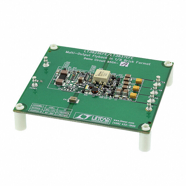
ICGOO电子元器件商城为您提供TPS55340EVM-147由Texas Instruments设计生产,在icgoo商城现货销售,并且可以通过原厂、代理商等渠道进行代购。 TPS55340EVM-147价格参考¥387.88-¥387.88。Texas InstrumentsTPS55340EVM-147封装/规格:评估板 - DC/DC 与 AC/DC(离线)SMPS, TPS55340 - DC/DC, Step Up or Down 1, Non-Isolated Outputs Evaluation Board。您可以下载TPS55340EVM-147参考资料、Datasheet数据手册功能说明书,资料中有TPS55340EVM-147 详细功能的应用电路图电压和使用方法及教程。
TPS55340EVM-147是德州仪器(Texas Instruments)推出的一款基于TPS55340升/降压控制器的评估板,适用于DC/DC与AC/DC(离线)SMPS应用。该评估板主要用于快速评估和开发宽输入电压范围下的高效电源转换系统,典型输入电压范围为4.5V至28V,可提供稳定的5V/3A输出。

其主要应用场景包括工业自动化、便携式设备、电信电源系统、电池供电设备以及分布式电源架构中的中间总线转换。由于具备升降压功能,它特别适用于输入电压可能高于或低于输出电压的场合,例如在电池电量变化较大的系统中保持稳定输出。

此外,该评估板也适用于需要高效率、小尺寸电源设计的研发项目,帮助工程师验证TPS55340在真实环境下的性能,如动态负载响应、效率表现、热管理及EMI特性。通过该EVM,用户可加快产品开发周期,优化电路设计,适用于各类中低功率电源系统的原型验证与测试。
| 参数 | 数值 |
| 产品目录 | 编程器,开发系统半导体 |
| 描述 | EVAL MODULE FOR TPS55340-147电源管理IC开发工具 TPS55340 SEPIC Eval Mod |
| 产品分类 | |
| 品牌 | Texas Instruments |
| 产品手册 | |
| 产品图片 | |
| rohs | 符合RoHS库存产品核实请求 / 库存产品核实请求 |
| 产品系列 | 电源管理IC开发工具,Texas Instruments TPS55340EVM-147- |
| 数据手册 | 点击此处下载产品Datasheethttp://www.ti.com/lit/pdf/slvu742 |
| 产品型号 | TPS55340EVM-147 |
| 主要用途 | DC/DC,步升/步降 |
| 产品 | Evaluation Modules |
| 产品种类 | 电源管理IC开发工具 |
| 使用的IC/零件 | TPS55340 |
| 其它名称 | 296-37520 |
| 制造商产品页 | http://www.ti.com/general/docs/suppproductinfo.tsp?distId=10&orderablePartNumber=TPS55340EVM-147 |
| 功率-输出 | - |
| 商标 | Texas Instruments |
| 工具用于评估 | TPS55340 |
| 工厂包装数量 | 1 |
| 所含物品 | 板 |
| 板类型 | 完全填充 |
| 标准包装 | 1 |
| 电压-输入 | 6 V ~ 18 V |
| 电压-输出 | 12V |
| 电流-输出 | 1A |
| 相关产品 | /product-detail/zh/TPS55340RTET/296-30530-2-ND/3314296/product-detail/zh/TPS55340RTET/296-30530-1-ND/3451657/product-detail/zh/TPS55340RTET/296-30530-6-ND/3451684/product-detail/zh/TPS55340RTER/296-37677-2-ND/3503781/product-detail/zh/TPS55340PWPR/TPS55340PWPR-ND/3727185/product-detail/zh/TPS55340PWP/296-35493-5-ND/3768420 |
| 稳压器拓扑 | - |
| 类型 | Voltage Regulators - Switching Regulators |
| 输入电压 | 6 V to 18 V |
| 输出和类型 | 1,非隔离 |
| 输出电压 | 12 V |
| 输出电流 | 1 A |
| 频率-开关 | 500kHz |


- 商务部:美国ITC正式对集成电路等产品启动337调查
- 曝三星4nm工艺存在良率问题 高通将骁龙8 Gen1或转产台积电
- 太阳诱电将投资9.5亿元在常州建新厂生产MLCC 预计2023年完工
- 英特尔发布欧洲新工厂建设计划 深化IDM 2.0 战略
- 台积电先进制程称霸业界 有大客户加持明年业绩稳了
- 达到5530亿美元!SIA预计今年全球半导体销售额将创下新高
- 英特尔拟将自动驾驶子公司Mobileye上市 估值或超500亿美元
- 三星加码芯片和SET,合并消费电子和移动部门,撤换高东真等 CEO
- 三星电子宣布重大人事变动 还合并消费电子和移动部门
- 海关总署:前11个月进口集成电路产品价值2.52万亿元 增长14.8%

PDF Datasheet 数据手册内容提取
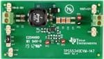
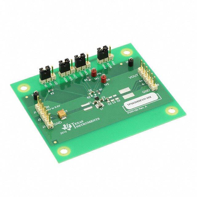
User's Guide SLVU742A–June2012–RevisedAugust2013 TPS55340EVM-147, 6V to 18V Input, 12V Output SEPIC Evaluation Module This user’s guide contains information for the TPS55340EVM-147 evaluation module (also called PWR147) as well as the TPS55340 DC/DC converter. The document includes the performance specifications,schematic,andthebillofmaterialsfortheTPS55340EVM-147. Contents 1 Background .................................................................................................................. 2 2 PerformanceSpecificationSummary..................................................................................... 2 3 Modifications ................................................................................................................. 3 4 TestSetupandResults .................................................................................................... 3 5 BoardLayout ............................................................................................................... 12 6 SchematicandBillofMaterials .......................................................................................... 15 ListofFigures 1 TPS55340EVM-147Efficiency............................................................................................ 4 2 TPS55340EVM-147OutputVoltageLoadRegulation................................................................. 5 3 TPS55340EVM-147OutputVoltageLineRegulation.................................................................. 5 4 TPS55340EVM-147V =6VTransientResponse..................................................................... 6 IN 5 TPS55340EVM-147V =18VTransientResponse................................................................... 6 IN 6 TPS55340EVM-147LoopResponse..................................................................................... 7 7 TPS55340EVM-147V =6VOutputRipple ............................................................................ 7 IN 8 TPS55340EVM-147V =18VOutputRipple........................................................................... 8 IN 9 TPS55340EVM-147DCMOutputRipple................................................................................ 8 10 TPS55340EVM-147V =18VPulse-Skipping.......................................................................... 9 IN 11 TPS55340EVM-147V =6VInputVoltageRipple..................................................................... 9 IN 12 TPS55340EVM-147V =18VInputVoltageRipple.................................................................. 10 IN 13 TPS55340EVM-147PowerUpWithEN ............................................................................... 10 14 TPS55340EVM-147PowerDownWithEN............................................................................ 11 15 TPS55340EVM-147PowerUpWithV ................................................................................ 11 IN 16 TPS55340EVM-147PowerDownWithV ............................................................................ 12 IN 17 TPS55340EVM-147Top-SideAssembly............................................................................... 13 18 TPS55340EVM-147Top-SideLayout.................................................................................. 13 19 TPS55340EVM-147InternalLayer-1Layout.......................................................................... 14 20 TPS55340EVM-147InternalLayer-2Layout.......................................................................... 14 21 TPS55340EVM-147Bottom-SideLayout .............................................................................. 15 22 TPS55340EVM-147Schematic.......................................................................................... 15 ListofTables 1 InputVoltageandOutputCurrentSummary............................................................................ 2 2 PerformanceSpecificationSummary..................................................................................... 2 3 EVMConnectorsandTestPoints........................................................................................ 4 4 TPS55340EVM-147BillofMaterials.................................................................................... 16 SLVU742A–June2012–RevisedAugust2013 TPS55340EVM-147,6Vto18VInput,12VOutputSEPICEvaluationModule 1 SubmitDocumentationFeedback Copyright©2012–2013,TexasInstrumentsIncorporated
Background www.ti.com 1 Background TheTPS55340DC/DCconverterisintypicalapplicationsastep-upboostconverter,howeverthisEVM usesitinaSEPICtopology.Ratedinputvoltageandoutputcurrentrangefortheevaluationmoduleare giveninTable1.ThisevaluationmoduledemonstratestheperformanceoftheTPS55340inanexample applicationandcanaccommodateevaluationofotherSEPICapplicationssupportedbytheTPS55340. Thisdesignshowsasmallprinted-circuit-boardareathatcanbeachievedwhendesigningwiththe TPS55340regulator.However,appropriatesizingoftheinductoranddiodeforthedesiredapplicationcan furtherreducetheboardarea.Theswitchingfrequencyisexternallysetatanominal500kHz.The40V, 5A,low-sideMOSFETisincorporatedinsidetheTPS55340packagealongwiththegatedrivecircuitry. Thelowdrain-to-sourceon-resistanceoftheMOSFETallowstheTPS55340toachievehighefficiencies. Thecompensationcomponentsareexternaltotheintegratedcircuit(IC).Inthisexampleapplicationthe absolutemaximuminputvoltagefortheTPS55340EVM-147is26V. Table1.InputVoltageandOutputCurrentSummary EVM InputVoltageRange MaximumOutputCurrent TPS55340EVM-147 V =6Vto18V I max=1A IN OUT 2 Performance Specification Summary Table2providesasummaryoftheTPS55340EVM-147performancespecifications.Specificationsare givenforaninputvoltageofV =6VandV =18Vwithanoutputvoltageof12V,unlessotherwise IN IN specified.Theambienttemperatureis25°Cforallmeasurements,unlessotherwisenoted. Table2. PerformanceSpecificationSummary Specification TestConditions Min Typ Max Unit VINvoltagerange 6 12 18 V Outputvoltagesetpoint 12 V Lineregulation IOUT=500mA,VIN=6Vto18V ±0.1% Operatingfrequency 500 kHz Outputcurrentrange .001 1 A Outputovercurrentlimit(1) VIN=6V 1.5 2.6 A Outputovercurrentlimit(1) VIN=18V 1.9 3.4 A Loadregulation IOUT=1mAto1A,VIN=6Vto18V ±0.1% IOUT=250mAto750mA, Voltagechange –480 mV VIN=6V Recoverytime 1 ms Loadtransientresponse IOUT=750mAto250mA, Voltagechange 480 mV VIN=6V Recoverytime 1 ms Loopbandwidth IOUT=1A,VIN=6V 6.3 kHz Phasemargin IOUT=1A,VIN=6V 59.3 ° Loopbandwidth IOUT=1A,VIN=18V 13.2 kHz Phasemargin IOUT=1A,VIN=18V 66.5 ° Outputripplevoltage IOUT=1A,VIN=6V 60 mVpp Outputripplevoltage IOUT=1A,VIN=18V 40 mVpp Maximumefficiency TPS55340EVM-147,VIN=6V,IOUT=350mA 92.1% Maximumefficiency TPS55340EVM-147,VIN=18V,IOUT=1A 92.1% (1) TheovercurrentlimitisdependentontheinputvoltageandbasedonpeakcurrentlimitoftheTPS55340. 2 TPS55340EVM-147,6Vto18VInput,12VOutputSEPICEvaluationModule SLVU742A–June2012–RevisedAugust2013 SubmitDocumentationFeedback Copyright©2012–2013,TexasInstrumentsIncorporated
www.ti.com Modifications 3 Modifications TheseevaluationmodulesprovideaccesstothefeaturesoftheTPS55340.Somemodificationstothis modulearepossible. 3.1 Output Voltage Set Point TheresistordividernetworkofR1andR2setstheoutputvoltage.KeepR2fixedatorcloseto10kΩ.To changetheoutputvoltageoftheEVM,changethevalueofresistorR1.CalculatethevalueofR1fora specificoutputvoltagebyusingEquation1. æ V ö R1=R2´ç OUT -1÷ è1.229V ø (1) NotethatV mustbeinarangesothattheon-timeisgreaterthantheminimumcontrollableon-time IN (77nstypical),andthemaximumdutycycleislessthan89%minimumand93%typical. Afteradjustingtheoutputvoltagethemaximuminputvoltagemustbetakenintoconsideration.The voltageontheinternalFET,theSWpin,isequaltothesumoftheinputvoltageandtheoutputvoltage. ByusingEquation2youcandeterminetherecommendedmaximuminputvoltage. V max=38V-V IN OUT (2) 3.2 Maximum Output Current Afteradjustinginputoroutputvoltagesettings,verifythemaximumoutputcurrentperEquation3 below, whereI isthepeakcurrentlimitoftheTPS55340andV istheforwardvoltagedropoftheexternal LIM F schottkydiode(D1).ThisequationcombinesEquations40,42,and44fromthedatasheet. § V min V +V · ¨I min- IN × OUT F ¸ © LIM 2×f ×L V +V +V min¹ I max= SW OUT F IN OUT § V · ¨ OUT +1¸ ©V min×(cid:24) ¹ IN EST (3) 3.3 Slow-Start Time Theslow-starttimecanbeadjustedbychangingthevalueofC3.TheEVMusesC3=0.047 µFas recommendedonthedatasheettoavoidanyovershootduringstart-up.Alargercapacitanceincreases theslow-starttimewhileasmallercapacitancedecreasesit. 3.4 Other Modifications Pleaseseedatasheetrecommendationsandequationswhenchangingtheswitchingfrequency, input/outputvoltagerange,inputinductor,outputcapacitorsorcompensation. 4 Test Setup and Results Thissectiondescribeshowtoproperlyconnect,setup,andusetheTPS55340EVM-147evaluation module.Includedaretestresultstypicalfortheevaluationmodulecoveringefficiency,outputvoltage regulation,loadtransients,loopresponse,outputripple,inputripple,start-upandshut-down. SLVU742A–June2012–RevisedAugust2013 TPS55340EVM-147,6Vto18VInput,12VOutputSEPICEvaluationModule 3 SubmitDocumentationFeedback Copyright©2012–2013,TexasInstrumentsIncorporated
TestSetupandResults www.ti.com 4.1 Input/Output Connections TheTPS55340EVM-147isprovidedwithinput/outputconnectorsandtestpointsasshowninTable3. Connectapowersupplycapableofsupplying5AtoJ6throughapairof20AWGwires.Thejumper acrossJP1intheONposition(1-2)mustbeinplace.ConnecttheloadtoJ7throughapairof20AWG wires.Themaximumloadcurrentcapabilitymustbeatleast1A.Wirelengthsmustbeminimizedto reducelossesinthewires.HeaderJ1providesaplacetomonitortheV inputvoltageswithJ3providing IN aconvenientgroundreference.UseJ2tomonitortheoutputvoltagewithJ4asthegroundreference. Table3.EVMConnectorsandTestPoints ReferenceDesignator Function J1 2-pinheaderforVINinputvoltageconnections J2 2-pinheaderforVOUTinputvoltageconnections J3,J4 2-pinheaderforGNDconnections J5 2-pinheaderforsynchronizingsignalandground J6 V inputvoltageconnector.(SeeTable1forV range.) IN IN JP1 3-pinheaderforenable.Installjumperfrompins1-2toenableorfrompins2-3todisable. TP1 SWtestpoint TP2 Testpointbetweenvoltagedividernetworkandoutput.Usedforloopresponsemeasurements. TP3 COMPtestpoint TP4 OutputvoltagetestpointatVOUTconnector TP5 GNDtestpointatVOUTconnector 4.2 Efficiency TheefficiencyofthisEVMpeaksataloadcurrentofabout300mAat6Vinputand1Aat18Vinput,then decreasesastheloadcurrentincreasestowardfullload.Figure1showstheefficiencyforthe TPS55340EVM-147atanambienttemperatureof25°C. 100 90 80 70 %) 60 y ( nc 50 e ci Effi 40 30 20 VIN = 6V 10 VIN = 12V VIN = 18V 0 0 0.5 1 Output Current (A) G001 Figure1.TPS55340EVM-147Efficiency Theefficiencymaybelowerathigherambienttemperatures,duetotemperaturevariationinthedrain-to- sourceresistanceoftheinternalMOSFET. 4 TPS55340EVM-147,6Vto18VInput,12VOutputSEPICEvaluationModule SLVU742A–June2012–RevisedAugust2013 SubmitDocumentationFeedback Copyright©2012–2013,TexasInstrumentsIncorporated
www.ti.com TestSetupandResults 4.3 Output Voltage Load Regulation Figure2 showstheloadregulationfortheTPS55340EVM-147. 0.5 0.4 0.3 %) n ( 0.2 o viati 0.1 e D e 0 g a olt −0.1 V ut p −0.2 ut O −0.3 VIN = 6V −0.4 VIN = 12V VIN = 18V −0.5 0 0.5 1 Output Current (A) G002 Figure2.TPS55340EVM-147OutputVoltageLoadRegulation Measurementsareforanambienttemperatureof25°C. 4.4 Output Voltage Line Regulation Figure3 showsthelineregulationfortheTPS55340EVM-147witha24Ω (500mA)load. 0.5 0.4 0.3 %) n ( 0.2 o viati 0.1 e D e 0 g a olt −0.1 V ut p −0.2 ut O −0.3 −0.4 IOUT = 500mA −0.5 6 7 8 9 10 11 12 13 14 15 16 17 18 Output Current (A) G003 Figure3.TPS55340EVM-147OutputVoltageLineRegulation SLVU742A–June2012–RevisedAugust2013 TPS55340EVM-147,6Vto18VInput,12VOutputSEPICEvaluationModule 5 SubmitDocumentationFeedback Copyright©2012–2013,TexasInstrumentsIncorporated
TestSetupandResults www.ti.com 4.5 Load Transients Figure4 andFigure5showtheTPS55340EVM-147responsetoloadtransients.Thecurrentstepisfrom 25%to75%ofmaximumratedloadata6Vinputanda18Vinputrespectively.Thecurrentstepslewrate is10mA/µs.Totalpeak-to-peakvoltagevariationisasshown,includingrippleandnoiseontheoutput. C3: I (500 mA/div) OUT C4: V AC Coupled (200 mV/div) OUT Timebase = 500 µs/div Figure4.TPS55340EVM-147V =6VTransientResponse IN C3: I (500 mA/div) OUT C4: V AC Coupled (200 mV/div) OUT Timebase = 500 µs/div Figure5.TPS55340EVM-147V =18VTransientResponse IN 6 TPS55340EVM-147,6Vto18VInput,12VOutputSEPICEvaluationModule SLVU742A–June2012–RevisedAugust2013 SubmitDocumentationFeedback Copyright©2012–2013,TexasInstrumentsIncorporated
www.ti.com TestSetupandResults 4.6 Loop Characteristics Figure6 showstheTPS55340EVM-147loop-responsecharacteristics.Gainandphaseplotsareshown forV voltagesof6Vand18Vwithloadcurrentsof1A. IN 60 180 VIN = 6V Gain VIN = 6V Phase 40 VIN = 18V Gain 120 VIN = 18V Phase 20 60 B) °) n (d 0 0 se ( ai ha G P −20 −60 −40 −120 −60 −180 100 1k 10k 100k 1M Frequency (Hz) G006 Figure6. TPS55340EVM-147LoopResponse 4.7 Output Voltage Ripple Figure7 showstheTPS55340EVM-147outputvoltagerippleandinductorcurrentripple.Theoutput currentistheratedfullloadof1AandV =6V.Theripplevoltageismeasureddirectlyacrosstheoutput IN capacitors. C2: SW (10.0 V/div) C3: I (1.00 A/div) Lb C4: I (1.00 A/div) La C1: V AC Coupled (50 mV/div) OUT Timebase = 2.00 µs/div Figure7.TPS55340EVM-147V =6VOutputRipple IN SLVU742A–June2012–RevisedAugust2013 TPS55340EVM-147,6Vto18VInput,12VOutputSEPICEvaluationModule 7 SubmitDocumentationFeedback Copyright©2012–2013,TexasInstrumentsIncorporated
TestSetupandResults www.ti.com Figure8 showstheTPS55340EVM-147outputvoltagerippleandinductorcurrentripple.Theoutput currentistheratedfullloadof1AandV =18V.Theripplevoltageismeasureddirectlyacrosstheoutput IN capacitors. C2: SW (20.0 V/div) C3: I (1.00 A/div) Lb C4: I (1.00 A/div) La C1: V AC Coupled (50 mV/div) OUT Timebase = 2.00 µs/div Figure8.TPS55340EVM-147V =18VOutputRipple IN Figure9 showstheTPS55340EVM-147outputvoltageripple,inductorcurrentrippleandswitching waveformwhileoperatingindiscontinuousconductionmode(DCM).Theinputvoltageis12Vandthe outputisloadedwith60Ω. C2: SW (20.0 V/div) C3: I (1.00 A/div) Lb C4: I (1.00 A/div) La C1: V AC Coupled (20 mV/div) OUT Timebase (2.00 µs/div) Figure9.TPS55340EVM-147DCMOutputRipple 8 TPS55340EVM-147,6Vto18VInput,12VOutputSEPICEvaluationModule SLVU742A–June2012–RevisedAugust2013 SubmitDocumentationFeedback Copyright©2012–2013,TexasInstrumentsIncorporated
www.ti.com TestSetupandResults 4.8 Pulse-Skipping Operation TheTPS55340featurespulse-skippingforoutputregulationwhenoperatingatlightloads.Figure9 shows theoutputvoltagerippleandthepulse-skippingatSW.Theinputvoltageis18V. C2: SW (20.0 V/div) C3: I (1.00 A/div) Lb C4: I (1.00 A/div) La C1: V AC Coupled (50 mV/div) OUT Timebase = 2.00 µs/div Figure10.TPS55340EVM-147V =18VPulse-Skipping IN 4.9 Input Voltage Ripple Figure11showstheTPS55340EVM-147inputvoltageripple.Theoutputcurrentistheratedfullloadof 1AatV =6V.TherippleismeasureddirectlyacrosstheinputcapacitorC2. IN C2: SW (10.0 V/div) C3: I (1.00 A/div) Lb C4: I (1.00 A/div) La C1: V AC Coupled (50 mV/div) IN Timebase = 2.00 µs/div Figure11.TPS55340EVM-147V =6VInputVoltageRipple IN SLVU742A–June2012–RevisedAugust2013 TPS55340EVM-147,6Vto18VInput,12VOutputSEPICEvaluationModule 9 SubmitDocumentationFeedback Copyright©2012–2013,TexasInstrumentsIncorporated
TestSetupandResults www.ti.com Figure12showstheTPS55340EVM-147inputvoltageripple.Theoutputcurrentistheratedfullloadof 1AatV =18V.TherippleismeasureddirectlyacrosstheinputcapacitorC2. IN C2: SW (20.0 V/div) C3: I (1.00 A/div) Lb C4: I (1.00 A/div) La C1: V AC Coupled (50 mV/div) IN Timebase = 2.00 µs/div Figure12.TPS55340EVM-147V =18VInputVoltageRipple IN 4.10 Powering Up and Down with EN Figure13showsthestart-upwaveformsfortheTPS55340EVM-147.Theinputvoltageis6V,theENgoes highandtheoutputvoltagerampsfrom0Vto12V.Theloadis120Ω. C3: V (2.00 V/div) IN C4: EN (2.00 V/div) C1: SW (20 V/div) C2: V (5.00 V/div) OUT Timebase = 1.00 ms/div Figure13.TPS55340EVM-147PowerUpWithEN 10 TPS55340EVM-147,6Vto18VInput,12VOutputSEPICEvaluationModule SLVU742A–June2012–RevisedAugust2013 SubmitDocumentationFeedback Copyright©2012–2013,TexasInstrumentsIncorporated
www.ti.com TestSetupandResults Figure14showstheshutdownwaveformsfortheTPS55340EVM-147.Theinputvoltageis6V.TheEN goeslowandtheoutputvoltagerampsfrom12Vto0V.Theloadis120Ω. C3: V (5.00 V/div) IN C4: EN (2.00 V/div) C1: SW (20 V/div) C2: V (5.00 V/div) OUT Timebase = 20.0 ms/div Figure14.TPS55340EVM-147PowerDownWithEN 4.11 Powering Up and Down with VIN Figure15showsthestart-upwaveformsfortheTPS55340EVM-147.Theinputvoltagerampswiththe inputvoltagepowersupplyandENistiedtoV .V rampsup,theconverterstartsswitchingandthe IN IN outputvoltagerampsto12V.Theloadis120Ω. C3: V (2.00 V/div) IN C1: SW (10.0 V/div) C2: V (5.00 V/div) OUT Timebase = 2.00 ms/div Figure15.TPS55340EVM-147PowerUpWithV IN SLVU742A–June2012–RevisedAugust2013 TPS55340EVM-147,6Vto18VInput,12VOutputSEPICEvaluationModule 11 SubmitDocumentationFeedback Copyright©2012–2013,TexasInstrumentsIncorporated
BoardLayout www.ti.com Figure16showstheshutdownwaveformsfortheTPS55340EVM-147.Theinputvoltagerampsdownwith theinputvoltagepowersupplyandENistiedtoV .WhenV islessthanthe2.6VtypicalUVLO,the IN IN converterstopsswitchingandtheoutputvoltagerampsdown.Theloadis120Ω. C3: V (2.00 V/div) IN C1: SW (10.0 V/div) C2: V (5.00 V/div) OUT Timebase = 5.00 ms/div Figure16. TPS55340EVM-147PowerDownWithV IN 5 Board Layout ThissectionprovidesadescriptionoftheTPS55340EVM-147boardlayoutandlayerillustrations. 5.1 Layout TheboardlayoutfortheTPS55340EVM-147isshowninFigure17throughFigure21.Thetop-sidelayer oftheEVMislaidoutinamannertypicalofauserapplication.Thetop,bottom,andinternallayersare2- oz.copper. ThetoplayercontainsthemainpowertracesforV ,V ,andSW.Alsoonthetoplayerareconnections IN OUT fortheremainingpinsoftheTPS55340andalargeareafilledwithground.Theinternallayersandbottom areprimarilygroundwithadditionalfillareasforV ,andV .Thetop-sidegroundtracesconnecttothe IN OUT bottomandinternalgroundplaneswithmultipleviasplacedaroundtheboard.Nineviasdirectlyunderthe TPS55340deviceprovideathermalpathfromthetop-sidegroundplanetothebottom-sidegroundplane. Placetheoutputdecouplingcapacitors(C8-C11)asclosetotheICaspossible.Thecopperareaofthe SWnodeiskeptsmalltominimizenoise.TheviasnearthediodeD1ontheV planeaidwiththermal OUT dissipation.Additionally,keepthevoltagesetpointresistordividercomponentsclosetotheIC.Thevoltage dividernetworktiestotheoutputvoltageatthepointofregulation,thecopperV traceattheJ7output OUT connector.FortheTPS55340,anadditionalinputbulkcapacitormaybenecessary,dependingonthe EVMconnectiontotheinputsupply.Criticalanalogcircuitssuchasthevoltagesetpointdivider,frequency setresistor,slow-startcapacitor,andcompensationcomponentsterminatetogroundbyusingaseparate groundtraceonthetopandbottomconnectedpowergroundpouronlyatonepointdirectlyundertheIC. 12 TPS55340EVM-147,6Vto18VInput,12VOutputSEPICEvaluationModule SLVU742A–June2012–RevisedAugust2013 SubmitDocumentationFeedback Copyright©2012–2013,TexasInstrumentsIncorporated
www.ti.com BoardLayout Figure17.TPS55340EVM-147Top-SideAssembly Figure18.TPS55340EVM-147Top-SideLayout SLVU742A–June2012–RevisedAugust2013 TPS55340EVM-147,6Vto18VInput,12VOutputSEPICEvaluationModule 13 SubmitDocumentationFeedback Copyright©2012–2013,TexasInstrumentsIncorporated
BoardLayout www.ti.com Figure19.TPS55340EVM-147InternalLayer-1Layout Figure20.TPS55340EVM-147InternalLayer-2Layout 14 TPS55340EVM-147,6Vto18VInput,12VOutputSEPICEvaluationModule SLVU742A–June2012–RevisedAugust2013 SubmitDocumentationFeedback Copyright©2012–2013,TexasInstrumentsIncorporated
www.ti.com SchematicandBillofMaterials Figure21.TPS55340EVM-147Bottom-SideLayout 6 Schematic and Bill of Materials ThissectionpresentstheTPS55340EVM-147schematicandbillofmaterials. 6.1 Schematic Figure22istheschematicfortheTPS55340EVM-147. L1 12uH Lb C6 TP4 VIN J1 La 2.2uF D1 J2 1 2 VIN VOUT 6-18V 2 TP1 1 12V, 1A J6 C1 C102uF R06 1 C228uF C229uF C221u0F C11 J7 VIN 1 1 1 2 VOUT 2 1 GND GND C7 1716151413 TP5 J3 0.1uF WPD SW SW NC GND 2 J4 2 1SW P PPGND12 R5 1 GND GND 1 2 11 VIN U1 PGND 49.9 3EN TPS55340RTE NC 10 9R5.43k TP2 4 9 SS FREQ OENN JP1 123 VIN C0.3047uF SYNC5AGND6COMP7FB8 TPS55340RTE R1 OFF SYNC 86.6k J5 1 SYNC TP3 SYNC 2 GND R2 R3 2.37k C5 10k 1 C4 0.1uF 1 Not Populated Figure22.TPS55340EVM-147Schematic SLVU742A–June2012–RevisedAugust2013 TPS55340EVM-147,6Vto18VInput,12VOutputSEPICEvaluationModule 15 SubmitDocumentationFeedback Copyright©2012–2013,TexasInstrumentsIncorporated
SchematicandBillofMaterials www.ti.com 6.2 Bill of Materials Table4presentsthebillofmaterialsfortheTPS55340EVM-147. Table4.TPS55340EVM-147BillofMaterials QTY RefDes Value Description Size PartNumber MFR 0 C1 Open Capacitor,Ceramic,35V,X7R,10% 1210 STD STD 1 C2 10uF Capacitor,Ceramic,36V,X7R,10% 1210 GRM32ER7YA106KA12L Murata 1 C3 0.047uF Capacitor,Ceramic,10V,X7R,10% 0603 STD STD 1 C4 0.1uF Capacitor,Ceramic,10v,X7R,10% 0603 STD STD 0 C5 Open Capacitor,Ceramic,10V,X7R,10% 0603 STD STD 1 C6 2.2uF Capacitor,Ceramic,50V,X7R,10% 1210 STD STD 1 C7 0.1uF Capacitor,Ceramic,50V,X7R,10% 0603 STD STD 3 C8-C10 22uF Capacitor,Ceramic,50V,X7R,10% 1210 STD STD 0 C11 Open Capacitor,Ceramic,50V,X7R,10% 1210 GRM32ER71H475KA88L Murata 1 D1 B340B Diode,SchottkyBarrierRectifier,3-A,40-V SMB B340B-13-F DiodesInc 5 J1-5 PEC025AAN Header,Male2-pin,100milspacing 0.100x2inch PEC025AAN Suffins 2 J6-7 ED555/2DS TerminalBLock,2-pin,6-A,3.5mm 0.27x0.25inch ED555/205 OST 1 JP1 PEC035AAN Header,Male3-pin,100milspacing 0.100x3inch PEC035AAN Sullins 1 L1 12uH Inductor,SMT,6.8A,74milliohm,±20% 0.484x0.484inch MSD1260-123ML Coilcraft 1 R1 86.6k Resistor,Chip,1/16W,1% 0603 STD STD 1 R2 10.0k Resistor,Chip,1/16W,1% 0603 STD 1 R3 2.37k Resistor,Chip,1/16W,1% 0603 STD 1 R4 95.3k Resistor,Chip,1/16W,1% 0603 STD 1 R5 49.9 Resistor,Chip,1/16W,1% 0603 STD 1 R6 0 Resistor,Chip,1/16W,1% 0603 STD 1 SH1 Shortjumper,100mil 0.100inch 929950-00 3M 1 TP5 5001 TestPoint,Black,ThruHoleColorKeyed 0.100x0.100inch Keystone 3 TP2-4 5000 TestPoint,Red,ThruHoleColorKeyed 0.100x0.100inch Keystone 0 TP1 Open TestPoint,Red,ThruHoleColorKeyed 0.100x0.100inch Keystone IC,5A40VBoostConverterwithSoft-startand 1 U1 TPS55340RTE QFN-16 TPS55340RTE TI ProgrammableSwitchingFrequency 1 – PCB,2.6Inx1.5Inx0.062In PWR147 Any Notes:1. TheseassembliesareESDsensitive,ESDprecautionsshallbeobserved. 2. Theseassembliesmustbecleanandfreefromfluxandallcontaminants.Useofnocleanfluxisnotacceptable. 3. TheseassembliesmustcomplywithworkmanshipstandardsIPC-A-610Class2. 4. Refdesignatorsmarkedwithanasterisk('**')cannotbesubstituted.AllothercomponentscanbesubstitutedwithequivalentMFG'scomponents. 6.3 Reference 1. TPS55340,Integrated5-A40-VBoost/SEPIC/FlybackConverterwithAdjustableSwitchingFrequency datasheet(SLVSBD4) 16 TPS55340EVM-147,6Vto18VInput,12VOutputSEPICEvaluationModule SLVU742A–June2012–RevisedAugust2013 SubmitDocumentationFeedback Copyright©2012–2013,TexasInstrumentsIncorporated
EVALUATIONBOARD/KIT/MODULE(EVM)ADDITIONALTERMS TexasInstruments(TI)providestheenclosedEvaluationBoard/Kit/Module(EVM)underthefollowingconditions: Theuserassumesallresponsibilityandliabilityforproperandsafehandlingofthegoods.Further,theuserindemnifiesTIfromallclaims arisingfromthehandlingoruseofthegoods. Shouldthisevaluationboard/kitnotmeetthespecificationsindicatedintheUser’sGuide,theboard/kitmaybereturnedwithin30daysfrom thedateofdeliveryforafullrefund.THEFOREGOINGLIMITEDWARRANTYISTHEEXCLUSIVEWARRANTYMADEBYSELLERTO BUYERANDISINLIEUOFALLOTHERWARRANTIES,EXPRESSED,IMPLIED,ORSTATUTORY,INCLUDINGANYWARRANTYOF MERCHANTABILITYORFITNESSFORANYPARTICULARPURPOSE.EXCEPTTOTHEEXTENTOFTHEINDEMNITYSETFORTH ABOVE,NEITHERPARTYSHALLBELIABLETOTHEOTHERFORANYINDIRECT,SPECIAL,INCIDENTAL,ORCONSEQUENTIAL DAMAGES. PleasereadtheUser'sGuideand,specifically,theWarningsandRestrictionsnoticeintheUser'sGuidepriortohandlingtheproduct.This noticecontainsimportantsafetyinformationabouttemperaturesandvoltages.ForadditionalinformationonTI'senvironmentaland/orsafety programs,pleasevisitwww.ti.com/eshorcontactTI. NolicenseisgrantedunderanypatentrightorotherintellectualpropertyrightofTIcoveringorrelatingtoanymachine,process,or combinationinwhichsuchTIproductsorservicesmightbeorareused.TIcurrentlydealswithavarietyofcustomersforproducts,and thereforeourarrangementwiththeuserisnotexclusive.TIassumesnoliabilityforapplicationsassistance,customerproductdesign, softwareperformance,orinfringementofpatentsorservicesdescribedherein. REGULATORYCOMPLIANCEINFORMATION AsnotedintheEVMUser’sGuideand/orEVMitself,thisEVMand/oraccompanyinghardwaremayormaynotbesubjecttotheFederal CommunicationsCommission(FCC)andIndustryCanada(IC)rules. ForEVMsnotsubjecttotheaboverules,thisevaluationboard/kit/moduleisintendedforuseforENGINEERINGDEVELOPMENT, DEMONSTRATIONOREVALUATIONPURPOSESONLYandisnotconsideredbyTItobeafinishedendproductfitforgeneralconsumer use.Itgenerates,uses,andcanradiateradiofrequencyenergyandhasnotbeentestedforcompliancewiththelimitsofcomputing devicespursuanttopart15ofFCCorICES-003rules,whicharedesignedtoprovidereasonableprotectionagainstradiofrequency interference.Operationoftheequipmentmaycauseinterferencewithradiocommunications,inwhichcasetheuserathisownexpensewill berequiredtotakewhatevermeasuresmayberequiredtocorrectthisinterference. GeneralStatementforEVMsincludingaradio UserPower/FrequencyUseObligations:Thisradioisintendedfordevelopment/professionaluseonlyinlegallyallocatedfrequencyand powerlimits.Anyuseofradiofrequenciesand/orpoweravailabilityofthisEVManditsdevelopmentapplication(s)mustcomplywithlocal lawsgoverningradiospectrumallocationandpowerlimitsforthisevaluationmodule.Itistheuser’ssoleresponsibilitytoonlyoperatethis radioinlegallyacceptablefrequencyspaceandwithinlegallymandatedpowerlimitations.Anyexceptionstothisarestrictlyprohibitedand unauthorizedbyTexasInstrumentsunlessuserhasobtainedappropriateexperimental/developmentlicensesfromlocalregulatory authorities,whichisresponsibilityofuserincludingitsacceptableauthorization. ForEVMsannotatedasFCC–FEDERALCOMMUNICATIONSCOMMISSIONPart15Compliant Caution Thisdevicecomplieswithpart15oftheFCCRules.Operationissubjecttothefollowingtwoconditions:(1)Thisdevicemaynotcause harmfulinterference,and(2)thisdevicemustacceptanyinterferencereceived,includinginterferencethatmaycauseundesiredoperation. Changesormodificationsnotexpresslyapprovedbythepartyresponsibleforcompliancecouldvoidtheuser'sauthoritytooperatethe equipment. FCCInterferenceStatementforClassAEVMdevices ThisequipmenthasbeentestedandfoundtocomplywiththelimitsforaClassAdigitaldevice,pursuanttopart15oftheFCCRules. Theselimitsaredesignedtoprovidereasonableprotectionagainstharmfulinterferencewhentheequipmentisoperatedinacommercial environment.Thisequipmentgenerates,uses,andcanradiateradiofrequencyenergyand,ifnotinstalledandusedinaccordancewiththe instructionmanual,maycauseharmfulinterferencetoradiocommunications.Operationofthisequipmentinaresidentialareaislikelyto causeharmfulinterferenceinwhichcasetheuserwillberequiredtocorrecttheinterferenceathisownexpense.
FCCInterferenceStatementforClassBEVMdevices ThisequipmenthasbeentestedandfoundtocomplywiththelimitsforaClassBdigitaldevice,pursuanttopart15oftheFCCRules. Theselimitsaredesignedtoprovidereasonableprotectionagainstharmfulinterferenceinaresidentialinstallation.Thisequipment generates,usesandcanradiateradiofrequencyenergyand,ifnotinstalledandusedinaccordancewiththeinstructions,maycause harmfulinterferencetoradiocommunications.However,thereisnoguaranteethatinterferencewillnotoccurinaparticularinstallation.If thisequipmentdoescauseharmfulinterferencetoradioortelevisionreception,whichcanbedeterminedbyturningtheequipmentoffand on,theuserisencouragedtotrytocorrecttheinterferencebyoneormoreofthefollowingmeasures: • Reorientorrelocatethereceivingantenna. • Increasetheseparationbetweentheequipmentandreceiver. • Connecttheequipmentintoanoutletonacircuitdifferentfromthattowhichthereceiverisconnected. • Consultthedealeroranexperiencedradio/TVtechnicianforhelp. ForEVMsannotatedasIC–INDUSTRYCANADACompliant ThisClassAorBdigitalapparatuscomplieswithCanadianICES-003. Changesormodificationsnotexpresslyapprovedbythepartyresponsibleforcompliancecouldvoidtheuser’sauthoritytooperatethe equipment. ConcerningEVMsincludingradiotransmitters ThisdevicecomplieswithIndustryCanadalicence-exemptRSSstandard(s).Operationissubjecttothefollowingtwoconditions:(1)this devicemaynotcauseinterference,and(2)thisdevicemustacceptanyinterference,includinginterferencethatmaycauseundesired operationofthedevice. ConcerningEVMsincludingdetachableantennas UnderIndustryCanadaregulations,thisradiotransmittermayonlyoperateusinganantennaofatypeandmaximum(orlesser)gain approvedforthetransmitterbyIndustryCanada.Toreducepotentialradiointerferencetootherusers,theantennatypeanditsgainshould besochosenthattheequivalentisotropicallyradiatedpower(e.i.r.p.)isnotmorethanthatnecessaryforsuccessfulcommunication. ThisradiotransmitterhasbeenapprovedbyIndustryCanadatooperatewiththeantennatypeslistedintheuserguidewiththemaximum permissiblegainandrequiredantennaimpedanceforeachantennatypeindicated.Antennatypesnotincludedinthislist,havingagain greaterthanthemaximumgainindicatedforthattype,arestrictlyprohibitedforusewiththisdevice. CetappareilnumériquedelaclasseAouBestconformeàlanormeNMB-003duCanada. Leschangementsoulesmodificationspasexpressémentapprouvésparlapartieresponsabledelaconformitéontpuviderl’autoritéde l'utilisateurpouractionnerl'équipement. ConcernantlesEVMsavecappareilsradio LeprésentappareilestconformeauxCNRd'IndustrieCanadaapplicablesauxappareilsradioexemptsdelicence.L'exploitationest autoriséeauxdeuxconditionssuivantes:(1)l'appareilnedoitpasproduiredebrouillage,et(2)l'utilisateurdel'appareildoitacceptertout brouillageradioélectriquesubi,mêmesilebrouillageestsusceptibled'encompromettrelefonctionnement. ConcernantlesEVMsavecantennesdétachables Conformémentàlaréglementationd'IndustrieCanada,leprésentémetteurradiopeutfonctionneravecuneantenned'untypeetd'ungain maximal(ouinférieur)approuvépourl'émetteurparIndustrieCanada.Danslebutderéduirelesrisquesdebrouillageradioélectriqueà l'intentiondesautresutilisateurs,ilfautchoisirletyped'antenneetsongaindesortequelapuissanceisotroperayonnéeéquivalente (p.i.r.e.)nedépassepasl'intensiténécessaireàl'établissementd'unecommunicationsatisfaisante. LeprésentémetteurradioaétéapprouvéparIndustrieCanadapourfonctionneraveclestypesd'antenneénumérésdanslemanuel d’usageetayantungainadmissiblemaximaletl'impédancerequisepourchaquetyped'antenne.Lestypesd'antennenoninclusdans cetteliste,oudontlegainestsupérieuraugainmaximalindiqué,sontstrictementinterditspourl'exploitationdel'émetteur. SPACER SPACER SPACER SPACER SPACER SPACER SPACER SPACER
【【ImportantNoticeforUsersofEVMsforRFProductsinJapan】】 ThisdevelopmentkitisNOTcertifiedasConfirmingtoTechnicalRegulationsofRadioLawofJapan IfyouusethisproductinJapan,youarerequiredbyRadioLawofJapantofollowtheinstructionsbelowwithrespecttothisproduct: 1. Usethisproductinashieldedroomoranyothertestfacilityasdefinedinthenotification#173issuedbyMinistryofInternalAffairsand CommunicationsonMarch28,2006,basedonSub-section1.1ofArticle6oftheMinistry’sRuleforEnforcementofRadioLawof Japan, 2. UsethisproductonlyafteryouobtainedthelicenseofTestRadioStationasprovidedinRadioLawofJapanwithrespecttothis product,or 3. UseofthisproductonlyafteryouobtainedtheTechnicalRegulationsConformityCertificationasprovidedinRadioLawofJapanwith respecttothisproduct.Also,pleasedonottransferthisproduct,unlessyougivethesamenoticeabovetothetransferee.Pleasenote thatifyoucouldnotfollowtheinstructionsabove,youwillbesubjecttopenaltiesofRadioLawofJapan. TexasInstrumentsJapanLimited (address)24-1,Nishi-Shinjuku6chome,Shinjuku-ku,Tokyo,Japan http://www.tij.co.jp 【無線電波を送信する製品の開発キットをお使いになる際の注意事項】 本開発キットは技術基準適合証明を受けておりません。 本製品のご使用に際しては、電波法遵守のため、以下のいずれかの措置を取っていただく必要がありますのでご注意ください。 1. 電波法施行規則第6条第1項第1号に基づく平成18年3月28日総務省告示第173号で定められた電波暗室等の試験設備でご使用いただく。 2. 実験局の免許を取得後ご使用いただく。 3. 技術基準適合証明を取得後ご使用いただく。 なお、本製品は、上記の「ご使用にあたっての注意」を譲渡先、移転先に通知しない限り、譲渡、移転できないものとします。 上記を遵守頂けない場合は、電波法の罰則が適用される可能性があることをご留意ください。 日本テキサス・インスツルメンツ株式会社 東京都新宿区西新宿6丁目24番1号 西新宿三井ビル http://www.tij.co.jp SPACER SPACER SPACER SPACER SPACER SPACER SPACER SPACER SPACER SPACER SPACER SPACER SPACER SPACER SPACER SPACER SPACER
EVALUATIONBOARD/KIT/MODULE(EVM) WARNINGS,RESTRICTIONSANDDISCLAIMERS ForFeasibilityEvaluationOnly,inLaboratory/DevelopmentEnvironments.Unlessotherwiseindicated,thisEVMisnotafinished electricalequipmentandnotintendedforconsumeruse.Itisintendedsolelyforuseforpreliminaryfeasibilityevaluationin laboratory/developmentenvironmentsbytechnicallyqualifiedelectronicsexpertswhoarefamiliarwiththedangersandapplicationrisks associatedwithhandlingelectricalmechanicalcomponents,systemsandsubsystems.Itshouldnotbeusedasallorpartofafinishedend product. YourSoleResponsibilityandRisk.Youacknowledge,representandagreethat: 1. YouhaveuniqueknowledgeconcerningFederal,Stateandlocalregulatoryrequirements(includingbutnotlimitedtoFoodandDrug Administrationregulations,ifapplicable)whichrelatetoyourproductsandwhichrelatetoyouruse(and/orthatofyouremployees, affiliates,contractorsordesignees)oftheEVMforevaluation,testingandotherpurposes. 2. Youhavefullandexclusiveresponsibilitytoassurethesafetyandcomplianceofyourproductswithallsuchlawsandotherapplicable regulatoryrequirements,andalsotoassurethesafetyofanyactivitiestobeconductedbyyouand/oryouremployees,affiliates, contractorsordesignees,usingtheEVM.Further,youareresponsibletoassurethatanyinterfaces(electronicand/ormechanical) betweentheEVMandanyhumanbodyaredesignedwithsuitableisolationandmeanstosafelylimitaccessibleleakagecurrentsto minimizetheriskofelectricalshockhazard. 3. SincetheEVMisnotacompletedproduct,itmaynotmeetallapplicableregulatoryandsafetycompliancestandards(suchasUL, CSA,VDE,CE,RoHSandWEEE)whichmaynormallybeassociatedwithsimilaritems.Youassumefullresponsibilitytodetermine and/orassurecompliancewithanysuchstandardsandrelatedcertificationsasmaybeapplicable.Youwillemployreasonable safeguardstoensurethatyouruseoftheEVMwillnotresultinanypropertydamage,injuryordeath,eveniftheEVMshouldfailto performasdescribedorexpected. 4. YouwilltakecareofproperdisposalandrecyclingoftheEVM’selectroniccomponentsandpackingmaterials. CertainInstructions.ItisimportanttooperatethisEVMwithinTI’srecommendedspecificationsandenvironmentalconsiderationsperthe userguidelines.ExceedingthespecifiedEVMratings(includingbutnotlimitedtoinputandoutputvoltage,current,power,and environmentalranges)maycausepropertydamage,personalinjuryordeath.Iftherearequestionsconcerningtheseratingspleasecontact aTIfieldrepresentativepriortoconnectinginterfaceelectronicsincludinginputpowerandintendedloads.Anyloadsappliedoutsideofthe specifiedoutputrangemayresultinunintendedand/orinaccurateoperationand/orpossiblepermanentdamagetotheEVMand/or interfaceelectronics.PleaseconsulttheEVMUser'sGuidepriortoconnectinganyloadtotheEVMoutput.Ifthereisuncertaintyastothe loadspecification,pleasecontactaTIfieldrepresentative.Duringnormaloperation,somecircuitcomponentsmayhavecasetemperatures greaterthan60°Caslongastheinputandoutputaremaintainedatanormalambientoperatingtemperature.Thesecomponentsinclude butarenotlimitedtolinearregulators,switchingtransistors,passtransistors,andcurrentsenseresistorswhichcanbeidentifiedusingthe EVMschematiclocatedintheEVMUser'sGuide.Whenplacingmeasurementprobesnearthesedevicesduringnormaloperation,please beawarethatthesedevicesmaybeverywarmtothetouch.Aswithallelectronicevaluationtools,onlyqualifiedpersonnelknowledgeable inelectronicmeasurementanddiagnosticsnormallyfoundindevelopmentenvironmentsshouldusetheseEVMs. AgreementtoDefend,IndemnifyandHoldHarmless.Youagreetodefend,indemnifyandholdTI,itslicensorsandtheirrepresentatives harmlessfromandagainstanyandallclaims,damages,losses,expenses,costsandliabilities(collectively,"Claims")arisingoutoforin connectionwithanyuseoftheEVMthatisnotinaccordancewiththetermsoftheagreement.ThisobligationshallapplywhetherClaims ariseunderlawoftortorcontractoranyotherlegaltheory,andeveniftheEVMfailstoperformasdescribedorexpected. Safety-CriticalorLife-CriticalApplications.Ifyouintendtoevaluatethecomponentsforpossibleuseinsafetycriticalapplications(such aslifesupport)whereafailureoftheTIproductwouldreasonablybeexpectedtocauseseverepersonalinjuryordeath,suchasdevices whichareclassifiedasFDAClassIIIorsimilarclassification,thenyoumustspecificallynotifyTIofsuchintentandenterintoaseparate AssuranceandIndemnityAgreement. MailingAddress:TexasInstruments,PostOfficeBox655303,Dallas,Texas75265 Copyright©2013,TexasInstrumentsIncorporated
IMPORTANTNOTICE TexasInstrumentsIncorporatedanditssubsidiaries(TI)reservetherighttomakecorrections,enhancements,improvementsandother changestoitssemiconductorproductsandservicesperJESD46,latestissue,andtodiscontinueanyproductorserviceperJESD48,latest issue.Buyersshouldobtainthelatestrelevantinformationbeforeplacingordersandshouldverifythatsuchinformationiscurrentand complete.Allsemiconductorproducts(alsoreferredtohereinas“components”)aresoldsubjecttoTI’stermsandconditionsofsale suppliedatthetimeoforderacknowledgment. TIwarrantsperformanceofitscomponentstothespecificationsapplicableatthetimeofsale,inaccordancewiththewarrantyinTI’sterms andconditionsofsaleofsemiconductorproducts.TestingandotherqualitycontroltechniquesareusedtotheextentTIdeemsnecessary tosupportthiswarranty.Exceptwheremandatedbyapplicablelaw,testingofallparametersofeachcomponentisnotnecessarily performed. TIassumesnoliabilityforapplicationsassistanceorthedesignofBuyers’products.Buyersareresponsiblefortheirproductsand applicationsusingTIcomponents.TominimizetherisksassociatedwithBuyers’productsandapplications,Buyersshouldprovide adequatedesignandoperatingsafeguards. TIdoesnotwarrantorrepresentthatanylicense,eitherexpressorimplied,isgrantedunderanypatentright,copyright,maskworkright,or otherintellectualpropertyrightrelatingtoanycombination,machine,orprocessinwhichTIcomponentsorservicesareused.Information publishedbyTIregardingthird-partyproductsorservicesdoesnotconstitutealicensetousesuchproductsorservicesorawarrantyor endorsementthereof.Useofsuchinformationmayrequirealicensefromathirdpartyunderthepatentsorotherintellectualpropertyofthe thirdparty,oralicensefromTIunderthepatentsorotherintellectualpropertyofTI. ReproductionofsignificantportionsofTIinformationinTIdatabooksordatasheetsispermissibleonlyifreproductioniswithoutalteration andisaccompaniedbyallassociatedwarranties,conditions,limitations,andnotices.TIisnotresponsibleorliableforsuchaltered documentation.Informationofthirdpartiesmaybesubjecttoadditionalrestrictions. ResaleofTIcomponentsorserviceswithstatementsdifferentfromorbeyondtheparametersstatedbyTIforthatcomponentorservice voidsallexpressandanyimpliedwarrantiesfortheassociatedTIcomponentorserviceandisanunfairanddeceptivebusinesspractice. TIisnotresponsibleorliableforanysuchstatements. Buyeracknowledgesandagreesthatitissolelyresponsibleforcompliancewithalllegal,regulatoryandsafety-relatedrequirements concerningitsproducts,andanyuseofTIcomponentsinitsapplications,notwithstandinganyapplications-relatedinformationorsupport thatmaybeprovidedbyTI.Buyerrepresentsandagreesthatithasallthenecessaryexpertisetocreateandimplementsafeguardswhich anticipatedangerousconsequencesoffailures,monitorfailuresandtheirconsequences,lessenthelikelihoodoffailuresthatmightcause harmandtakeappropriateremedialactions.BuyerwillfullyindemnifyTIanditsrepresentativesagainstanydamagesarisingoutoftheuse ofanyTIcomponentsinsafety-criticalapplications. Insomecases,TIcomponentsmaybepromotedspecificallytofacilitatesafety-relatedapplications.Withsuchcomponents,TI’sgoalisto helpenablecustomerstodesignandcreatetheirownend-productsolutionsthatmeetapplicablefunctionalsafetystandardsand requirements.Nonetheless,suchcomponentsaresubjecttotheseterms. NoTIcomponentsareauthorizedforuseinFDAClassIII(orsimilarlife-criticalmedicalequipment)unlessauthorizedofficersoftheparties haveexecutedaspecialagreementspecificallygoverningsuchuse. OnlythoseTIcomponentswhichTIhasspecificallydesignatedasmilitarygradeor“enhancedplastic”aredesignedandintendedforusein military/aerospaceapplicationsorenvironments.BuyeracknowledgesandagreesthatanymilitaryoraerospaceuseofTIcomponents whichhavenotbeensodesignatedissolelyattheBuyer'srisk,andthatBuyerissolelyresponsibleforcompliancewithalllegaland regulatoryrequirementsinconnectionwithsuchuse. TIhasspecificallydesignatedcertaincomponentsasmeetingISO/TS16949requirements,mainlyforautomotiveuse.Inanycaseofuseof non-designatedproducts,TIwillnotberesponsibleforanyfailuretomeetISO/TS16949. Products Applications Audio www.ti.com/audio AutomotiveandTransportation www.ti.com/automotive Amplifiers amplifier.ti.com CommunicationsandTelecom www.ti.com/communications DataConverters dataconverter.ti.com ComputersandPeripherals www.ti.com/computers DLP®Products www.dlp.com ConsumerElectronics www.ti.com/consumer-apps DSP dsp.ti.com EnergyandLighting www.ti.com/energy ClocksandTimers www.ti.com/clocks Industrial www.ti.com/industrial Interface interface.ti.com Medical www.ti.com/medical Logic logic.ti.com Security www.ti.com/security PowerMgmt power.ti.com Space,AvionicsandDefense www.ti.com/space-avionics-defense Microcontrollers microcontroller.ti.com VideoandImaging www.ti.com/video RFID www.ti-rfid.com OMAPApplicationsProcessors www.ti.com/omap TIE2ECommunity e2e.ti.com WirelessConnectivity www.ti.com/wirelessconnectivity MailingAddress:TexasInstruments,PostOfficeBox655303,Dallas,Texas75265 Copyright©2013,TexasInstrumentsIncorporated