ICGOO在线商城 > 集成电路(IC) > PMIC - 稳压器 - DC DC 开关稳压器 > TPS54618RTER
 Datasheet下载
- 型号: TPS54618RTER
- 制造商: Texas Instruments
- 库位|库存: xxxx|xxxx
- 要求:
| 数量阶梯 | 香港交货 | 国内含税 |
| +xxxx | $xxxx | ¥xxxx |
查看当月历史价格
查看今年历史价格
TPS54618RTER产品简介:
ICGOO电子元器件商城为您提供TPS54618RTER由Texas Instruments设计生产,在icgoo商城现货销售,并且可以通过原厂、代理商等渠道进行代购。 TPS54618RTER价格参考。Texas InstrumentsTPS54618RTER封装/规格:PMIC - 稳压器 - DC DC 开关稳压器, 可调式 降压 开关稳压器 IC 正 0.799V 1 输出 6A 16-WFQFN 裸露焊盘。您可以下载TPS54618RTER参考资料、Datasheet数据手册功能说明书,资料中有TPS54618RTER 详细功能的应用电路图电压和使用方法及教程。
TPS54618RTER是德州仪器(Texas Instruments)推出的一款高效同步降压DC-DC开关稳压器,适用于多种应用场景,尤其适合需要高效率、小尺寸和高性能电源管理的系统。

 应用场景:

1. 通信设备:
   - TPS54618RTER广泛应用于通信基站、路由器、交换机等设备中。这些设备通常需要稳定的电源供应以确保数据传输的可靠性和稳定性。该芯片能够提供高达6A的连续输出电流,支持宽输入电压范围(4.5V至60V),适应不同电源输入条件,如电池供电或工业电源。

2. 工业自动化:
   - 在工业控制系统、PLC(可编程逻辑控制器)、伺服驱动器等应用中,TPS54618RTER可以为微处理器、传感器和其他关键组件提供稳定高效的电源。其高效率和低静态电流特性有助于延长系统的运行时间和可靠性,同时减少发热问题。

3. 汽车电子:
   - 该芯片适用于汽车信息娱乐系统、车载导航、ADAS(高级驾驶辅助系统)等应用。它能够在严苛的汽车环境中工作,支持冷启动和负载突降等极端情况。此外,其快速瞬态响应能力有助于保持输出电压的稳定,确保敏感电子元件正常工作。

4. 消费电子产品:
   - 在笔记本电脑、平板电脑、智能手机等便携式设备中,TPS54618RTER可以为内部电路提供高效稳定的电源。其紧凑的设计和低功耗特性使得它可以集成到空间受限的小型设备中,同时保持高效的电源转换效率。

5. 医疗设备:
   - 医疗设备如监护仪、超声波设备等对电源的稳定性和可靠性要求极高。TPS54618RTER凭借其高精度的输出电压调节和良好的抗干扰性能,成为这些设备的理想选择。它还可以帮助减小设备的尺寸和重量,提升便携性。

总之,TPS54618RTER凭借其出色的性能和广泛的适用性,成为众多领域中电源管理解决方案的首选。
| 参数 | 数值 |
| 产品目录 | 集成电路 (IC)半导体 |
| 描述 | IC REG BUCK SYNC ADJ 6A 16WQFN稳压器—开关式稳压器 2.95-6Vin,6A,2MHz Sync Step Down SWIFT |
| DevelopmentKit | TPS54618EVM-606 |
| 产品分类 | |
| 品牌 | Texas Instruments |
| 产品手册 | http://www.ti.com/litv/slvsae9d |
| 产品图片 |
|
| rohs | 符合RoHS无铅 / 符合限制有害物质指令(RoHS)规范要求 |
| 产品系列 | 电源管理 IC,稳压器—开关式稳压器,Texas Instruments TPS54618RTERSWIFT™ |
| 数据手册 | |
| 产品型号 | TPS54618RTER |
| PCN组件/产地 | |
| PCN设计/规格 | |
| PWM类型 | 电流模式 |
| 产品培训模块 | http://www.digikey.cn/PTM/IndividualPTM.page?site=cn&lang=zhs&ptm=25886 |
| 产品种类 | 稳压器—开关式稳压器 |
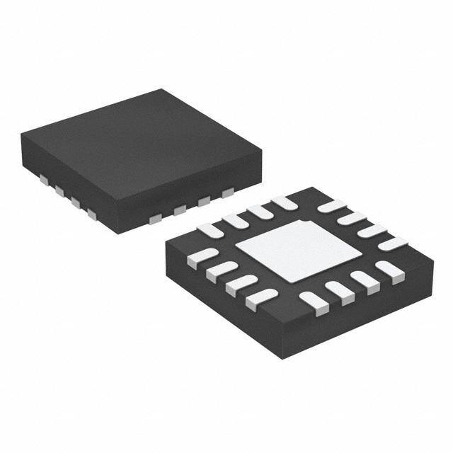
| 供应商器件封装 | 16-WQFN(3x3) |
| 关闭 | Shutdown |
| 其它名称 | 296-28148-6 |
| 制造商产品页 | http://www.ti.com/general/docs/suppproductinfo.tsp?distId=10&orderablePartNumber=TPS54618RTER |
| 包装 | Digi-Reel® |
| 参考设计库 | http://www.digikey.com/rdl/4294959904/4294959903/777 |
| 同步整流器 | 是 |
| 商标 | Texas Instruments |
| 商标名 | SWIFT |
| 安装类型 | 表面贴装 |
| 安装风格 | SMD/SMT |
| 封装 | Reel |
| 封装/外壳 | 16-WFQFN 裸露焊盘 |
| 封装/箱体 | WQFN-16 |
| 工作温度 | -40°C ~ 150°C |
| 工作温度范围 | - 40 C to + 150 C |
| 工厂包装数量 | 3000 |
| 开关频率 | 500 kHz |
| 拓扑结构 | Buck |
| 最大工作温度 | + 150 C |
| 最大输入电压 | 6 V |
| 最小工作温度 | - 40 C |
| 最小输入电压 | 2.95 V |
| 标准包装 | 1 |
| 特色产品 | http://www.digikey.com/cn/zh/ph/texas-instruments/tps54618.html |
| 电压-输入 | 2.95 V ~ 6 V |
| 电压-输出 | 0.8 V ~ 4.5 V |
| 电流-输出 | 6A |
| 电源电压-最小 | 2.95 V |
| 电源电流 | 515 uA |
| 类型 | 降压(降压) |
| 系列 | TPS54618 |
| 设计资源 | http://www.digikey.com/product-highlights/cn/zh/texas-instruments-webench-design-center/3176 |
| 输入电压 | 2.95 V to 6 V |
| 输出数 | 1 |
| 输出电压 | 1.8 V |
| 输出电流 | 6 A |
| 输出端数量 | 1 Output |
| 输出类型 | 可调式 |
| 配用 | /product-detail/zh/TPS54618EVM-606/296-28145-ND/2514723 |
| 频率-开关 | 500kHz |


- 商务部:美国ITC正式对集成电路等产品启动337调查
- 曝三星4nm工艺存在良率问题 高通将骁龙8 Gen1或转产台积电
- 太阳诱电将投资9.5亿元在常州建新厂生产MLCC 预计2023年完工
- 英特尔发布欧洲新工厂建设计划 深化IDM 2.0 战略
- 台积电先进制程称霸业界 有大客户加持明年业绩稳了
- 达到5530亿美元!SIA预计今年全球半导体销售额将创下新高
- 英特尔拟将自动驾驶子公司Mobileye上市 估值或超500亿美元
- 三星加码芯片和SET,合并消费电子和移动部门,撤换高东真等 CEO
- 三星电子宣布重大人事变动 还合并消费电子和移动部门
- 海关总署:前11个月进口集成电路产品价值2.52万亿元 增长14.8%


PDF Datasheet 数据手册内容提取
Product Order Technical Tools & Support & Folder Now Documents Software Community TPS54618 SLVSAE9F–NOVEMBER2010–REVISEDMAY2019 TPS54618 2.95-V to 6-V, 6-A, Synchronous Step-Down SWIFT™ Converter 1 Features 3 Description • Two12-mΩ (typical)MOSFETsforhighefficiency The TPS54618 device is a full-featured 6-V, 6-A, 1 synchronous step-down current-mode converter with at6-Aloads twointegratedMOSFETs. • 300-kHzto2-MHzswitchingfrequency The TPS54618 enables small designs by integrating • 0.8-V ±1%Voltagereferenceovertemperature the MOSFETs, implementing current-mode control to (–40°Cto+150°C) reduce external component count, reducing inductor • Synchronizestoexternalclock size by enabling up to 2-MHz switching frequency, • Adjustableslowstartandsequencing and minimizing the IC footprint with a small, 3-mm × 3-mm,thermally-enhancedWQFNpackage. • UVandOVpower-goodoutput • –40°Cto150°COperatingJunctionTemperature The TPS54618 provides accurate regulation for a Range variety of loads with an accurate ±1% voltage reference(VREF)overtemperature. • Thermallyenhanced3-mm× 3-mm,16-pinWQFN package Efficiencyismaximizedthroughtheintegrated • Pin-CompatibletoTPS54418 12-mΩ MOSFETs and 515-μA typical supply current. Using the enable pin, shutdown supply current is • CreateacustomdesignusingtheTPS54618with reducedto5.5-µAbyenteringashutdownmode. theWEBENCH®PowerDesigner Undervoltage lockout is internally set at 2.6 V, but 2 Applications can be increased by programming the threshold with a resistor network on the enable pin. The output- • Low-voltage,high-densitypowersystems voltage start-up ramp is controlled by the slow-start • Point-of-loadregulationforhigh-performance pin. An open-drain power-good signal indicates the DSPs,FPGAs,ASICs,andmicroprocessors outputiswithin93%to107%ofitsnominalvoltage. • Broadband,networking,andoptical Frequencyfoldbackandthermalshutdown protect the communicationsinfrastructure deviceduringanovercurrentcondition. For more SWIFT™ documentation, see the TI websiteatwww.ti.com/swift. DeviceInformation(1) PARTNUMBER PACKAGE BODYSIZE(NOM) TPS54618 WQFN(16) 3.00mm×3.00mm (1) For all available packages, see the orderable addendum at theendofthedatasheet. SimplifiedSchematic EfficiencyvsOutputCurrent 100 VIN TPS54618 95 3 Vin VIN BOOT 90 5 Vin 85 EPNWRGD PH VOUT Efficiency - % 778050 65 VSENSE 60 RSST/CLK 55 fVso=u t5 =0 01k.8HVz COMP 500 1 2 3 4 5 6 GND IO- Output Current -A AGND PowerPad 1 An IMPORTANT NOTICE at the end of this data sheet addresses availability, warranty, changes, use in safety-critical applications, intellectualpropertymattersandotherimportantdisclaimers.PRODUCTIONDATA.
TPS54618 SLVSAE9F–NOVEMBER2010–REVISEDMAY2019 www.ti.com Table of Contents 1 Features.................................................................. 1 7.4 DeviceFunctionalModes........................................19 2 Applications........................................................... 1 8 ApplicationandImplementation........................ 23 3 Description............................................................. 1 8.1 ApplicationInformation............................................23 4 RevisionHistory..................................................... 2 8.2 TypicalApplication..................................................23 5 PinConfigurationandFunctions......................... 3 9 PowerSupplyRecommendations...................... 31 6 Specifications......................................................... 4 10 Layout................................................................... 31 6.1 AbsoluteMaximumRatings......................................4 10.1 LayoutGuidelines.................................................31 6.2 ESDRatings..............................................................4 10.2 LayoutExample....................................................32 6.3 RecommendedOperatingConditions.......................4 10.3 PowerDissipationEstimate..................................32 6.4 ThermalInformation..................................................4 11 DeviceandDocumentationSupport................. 34 6.5 ElectricalCharacteristics...........................................5 11.1 DeviceSupport......................................................34 6.6 TimingRequirements................................................6 11.2 ReceivingNotificationofDocumentationUpdates34 6.7 TypicalCharacteristics..............................................7 11.3 CommunityResources..........................................34 7 DetailedDescription............................................ 11 11.4 Trademarks...........................................................34 7.1 Overview.................................................................11 11.5 ElectrostaticDischargeCaution............................34 7.2 FunctionalBlockDiagram.......................................12 11.6 Glossary................................................................34 7.3 FeatureDescription.................................................12 12 Mechanical,Packaging,andOrderable Information........................................................... 35 4 Revision History NOTE:Pagenumbersforpreviousrevisionsmaydifferfrompagenumbersinthecurrentversion. ChangesfromRevisionE(November2015)toRevisionF Page • Editorialchangesonly,notechnicalrevisions;addlinksforWEBENCH .............................................................................. 1 ChangesfromRevisionD(November2013)toRevisionE Page • AddedESDRatingstable,FeatureDescriptionsection,DeviceFunctionalModessection,Applicationand Implementationsection,PowerSupplyRecommendationssection,Layoutsection,DeviceandDocumentation Supportsection,andMechanical,Packaging,andOrderableInformationsection................................................................ 1 ChangesfromRevisionC(September2013)toRevisionD Page • Changedtitleofdatasheet..................................................................................................................................................... 1 • ChangedENpinmaximumratingfrom3.3Vto4.0VinAbsoluteMaximumRatings.......................................................... 4 • ChangedRT/CLKpinmaximumratingfrom3.3Vto4.0VinAbsoluteMaximumRatings.................................................. 4 ChangesfromRevisionB(October2012)toRevisionC Page • ChangedallThermalInformationvalues................................................................................................................................ 4 ChangesfromRevisionA(November2010)toRevisionB Page • ChangedENpinmaximumratingfrom3.3Vto4.0VinAbsoluteMaximumRatings.......................................................... 4 ChangesfromOriginal(November2010)toRevisionA Page • ChangedFigure5inTypicalCharacteristics.......................................................................................................................... 7 2 SubmitDocumentationFeedback Copyright©2010–2019,TexasInstrumentsIncorporated ProductFolderLinks:TPS54618
TPS54618 www.ti.com SLVSAE9F–NOVEMBER2010–REVISEDMAY2019 5 Pin Configuration and Functions RTEPackage 16-PinWQFNWithExposedThermalPad TopView D G T R O VIN EN PW BO 16 15 14 13 VIN 1 12 PH VIN 2 11 PH Thermal GND 3 Pad 10 PH GND 4 9 SS/TR 5 6 7 8 D E P K N S M L G N O C A E C T/ S R V PinFunctions PIN TYPE(1) DESCRIPTION NAME NO. AGND 5 G AnaloggroundshouldbeelectricallyconnectedtoGNDclosetothedevice. AbootstrapcapacitorisrequiredbetweenBOOTandPH.Ifthevoltageonthiscapacitorisbelowthe BOOT 13 I minimumrequiredbytheBOOTUVLO,theoutputisforcedtoswitchoffuntilthecapacitorisrefreshed. Erroramplifieroutput,andinputtotheoutputswitchcurrentcomparator.Connectfrequency COMP 7 O compensationcomponentstothispin. Enablepin,internalpullupcurrentsource.Pullbelow1.2Vtodisable.Floattoenable.Canbeusedto EN 15 I settheon/offthreshold(adjustUVLO)withtwoadditionalresistors. 3 GND G Powerground.Thispinshouldbeelectricallyconnecteddirectlytothepowerpadunderthedevice. 4 10 Thesourceoftheinternalhigh-sidepowerMOSFET,anddrainoftheinternallow-side(synchronous) PH 11 O rectifierMOSFET. 12 Anopen-drainoutput,assertslowifoutputvoltageislowduetothermalshutdown,overcurrent, PWRGD 14 O over/undervoltageorENshutdown. RT/CLK 8 I/O Resistortimingorexternalclockinputpin Slow-startandtracking.Anexternalcapacitorconnectedtothispinsetstheoutputvoltagerisetime. SS/TR 9 I/O Thispincanalsobeusedfortracking. 1 VIN 2 I Inputsupplyvoltage,2.95Vto6V 16 VSENSE 6 I Invertingnodeofthetransconductance(gm)erroramplifier Thermal GNDpinshouldbeconnectedtotheexposedpowerpadforproperoperation.Thispowerpadshould — G Pad beconnectedtoanyinternalPCBgroundplaneusingmultipleviasforgoodthermalperformance. (1) I=Input,O=Output,G=Ground Copyright©2010–2019,TexasInstrumentsIncorporated SubmitDocumentationFeedback 3 ProductFolderLinks:TPS54618
TPS54618 SLVSAE9F–NOVEMBER2010–REVISEDMAY2019 www.ti.com 6 Specifications 6.1 Absolute Maximum Ratings overoperatingfree-airtemperaturerange(unlessotherwisenoted)(1) MIN MAX UNIT PWRGD,VIN –0.3 7 EN,RT/CLK –0.3 4 Inputvoltage V COMP,SS,VSENSE –0.3 3 BOOT V +7 PH BOOT-PH 7 Outputvoltage PH –0.6 7 V PH(10-nstransient) –2 10 Sourcecurrent EN,RT/CLK 100 µA COMP,SS 100 µA Sinkcurrent PWRGD 10 mA Operatingjunctiontemperature,T –40 150 °C J Storagetemperature,T –65 150 °C stg (1) StressesbeyondthoselistedunderAbsoluteMaximumRatingsmaycausepermanentdamagetothedevice.Thesearestressratings only,whichdonotimplyfunctionaloperationofthedeviceattheseoranyotherconditionsbeyondthoseindicatedunderRecommended OperatingConditions.Exposuretoabsolute-maximum-ratedconditionsforextendedperiodsmayaffectdevicereliability. 6.2 ESD Ratings VALUE UNIT Human-bodymodel(HBM),perAECQ100-002(1) ±2000 V Electrostaticdischarge V (ESD) Charged-devicemodel(CDM),perAECQ100-011 ±750 (1) AECQ100-002indicatesthatHBMstressingshallbeinaccordancewiththeANSI/ESDA/JEDECJS-001specification. 6.3 Recommended Operating Conditions overoperatingfree-airtemperaturerange(unlessotherwisenoted) MIN MAX UNIT V Inputvoltage 3 6 V VIN T Operatingjunctiontemperature –40 150 °C A 6.4 Thermal Information TPS54618 THERMALMETRIC(1)(2) RTE(WQFN) UNIT 16PINS R Junction-to-ambientthermalresistance 44.38 °C/W θJA R Junction-to-case(top)thermalresistance 46.09 °C/W θJC(top) R Junction-to-boardthermalresistance 15.96 °C/W θJB ψ Junction-to-topcharacterizationparameter 0.69 °C/W JT ψ Junction-to-boardcharacterizationparameter 15.91 °C/W JB R Junction-to-case(bottom)thermalresistance 4.55 °C/W θJC(bot) (1) Unlessotherwisespecified,metricslistedinthistablerefertoJEDEChigh-Kboardmeasurements (2) Formoreinformationabouttraditionalandnewthermalmetrics,seetheSemiconductorandICPackageThermalMetricsapplication report,SPRA953. 4 SubmitDocumentationFeedback Copyright©2010–2019,TexasInstrumentsIncorporated ProductFolderLinks:TPS54618
TPS54618 www.ti.com SLVSAE9F–NOVEMBER2010–REVISEDMAY2019 6.5 Electrical Characteristics atT =–40°Cto150°C,VIN=2.95to6V(unlessotherwisenoted) J PARAMETER TESTCONDITIONS MIN TYP MAX UNIT SUPPLYVOLTAGE(VINPIN) Operatinginputvoltage 2.95 6 V VINUVLOSTOP 2.28 2.5 Internalundervoltagelockoutthreshold V VINUVLOSTART 2.45 2.6 Shutdownsupplycurrent EN=0V,25°C,2.95V≤VIN≤6V 5.5 15 μA Quiescentcurrent,I VSENSE=0.9V,VIN=5V,25°C,RT=400kΩ 515 650 μA q ENABLEANDUVLO(ENPIN) Rising 1.25 Enablethreshold V Falling 1.18 Enablethreshold+50mV –3.5 Inputcurrent μA Enablethreshold–50mV –1.9 VOLTAGEREFERENCE(VSENSEPIN) Voltagereference 2.95V≤VIN≤6V,–40°C<T <150°C 0.791 0.799 0.807 V J MOSFET BOOT-PH=5V 12 25 High-sideswitchresistance mΩ BOOT-PH=2.95V 16 33 VIN=5V 13 25 Low-sideswitchresistance mΩ VIN=2.95V 17 33 ERRORAMPLIFIER Inputcurrent 2 nA Erroramplifiertransconductance(gm) –2μA<I <2μA,V )=1V 245 μmhos (COMP) (COMP Erroramplifiertransconductance(gm) –2μA<I <2μA,V =1V, (COMP) (COMP) 79 μmhos duringslow-start Vsense=0.4V Erroramplifiersource/sink V =1V,100-mVoverdrive ±20 μA (COMP) COMPtoIswitchgm 25 A/V CURRENTLIMIT VIN=6V,25°C<T <150°C 7.46 10.6 15.3 J Currentlimitthreshold A VIN=2.95V,25°C<T <150°C 7.68 10.2 13.5 J THERMALSHUTDOWN Thermalshutdown 168 °C Hysteresis 20 °C BOOT(BOOTPIN) BOOTchargeresistance VIN=5V 16 Ω BOOT-PHUVLO VIN=2.95V 2.1 V SLOW-STARTANDTRACKING(SS/TRPIN) Chargecurrent V =0.4V 2 μA (SS/TR) SS/TRtoVSENSEmatching V =0.4V 54 mV (SS/TR) SS/TRtoreferencecrossover 98%normal 1.1 V SS/TRdischargevoltage(Overload) VSENSE=0V 61 mV SS/TRdischargecurrent(Overload) VSENSE=0V,V =0.4V 350 µA (SS/TR) SSdischargecurrent(UVLO,EN,Thermal VIN=5V,V(SS)=0.5V 1.9 mA fault) Copyright©2010–2019,TexasInstrumentsIncorporated SubmitDocumentationFeedback 5 ProductFolderLinks:TPS54618
TPS54618 SLVSAE9F–NOVEMBER2010–REVISEDMAY2019 www.ti.com Electrical Characteristics (continued) atT =–40°Cto150°C,VIN=2.95to6V(unlessotherwisenoted) J PARAMETER TESTCONDITIONS MIN TYP MAX UNIT POWERGOOD(PWRGDPIN) VSENSEfalling(Fault) 91% VSENSErising(Good) 93% VSENSEthreshold Vre VSENSErising(Fault) 109% VSENSEfalling(Good) 107% Hysteresis VSENSEfalling 2% Vref Outputhighleakage VSENSE=VREF,V =5.5V 7 nA (PWRGD) ON-resistance 56 100 Ω Outputlow I =3mA 0.2 0.3 V (PWRGD) MinimumVINforvalidoutput V <0.5Vat100μA 0.65 1.5 V (PWRGD) 6.6 Timing Requirements PARAMETER TESTCONDITIONS MIN NOM MAX UNIT TIMINGRESISTORANDEXTERNALCLOCK(RT/CLKPIN) SwitchingfrequencyrangeusingRTmode 200 2000 kHz Switchingfrequency Rt=400kΩ 400 500 600 kHz SwitchingfrequencyrangeusingCLKmode 300 2000 kHz MinimumCLKpulsewidth 75 ns RT/CLKvoltage R =400kΩ 0.5 V (RT/CLK) RT/CLKhighthreshold 1.6 2.2 V RT/CLKlowthreshold 0.4 0.6 V RT/CLKfallingedgetoPHrisingedgedelay Measureat500kHzwithRTresistorinseries 90 ns PLLlockintime Measureat500kHz 42 μs PH(PHPIN) Measuredat50%pointsonPH,I =3A 75 OUT MinimumON-time Measuredat50%pointsonPH,VIN=6V, ns 120 I =0A OUT Priortoskippingoffpulses,BOOT-PH=2.95V, MinimumOFF-time 60 ns I =3A OUT Risetime VIN=6V,6A 2.25 V/ns Falltime VIN=6V,6A 2 6 SubmitDocumentationFeedback Copyright©2010–2019,TexasInstrumentsIncorporated ProductFolderLinks:TPS54618
TPS54618 www.ti.com SLVSAE9F–NOVEMBER2010–REVISEDMAY2019 6.7 Typical Characteristics W 0.025 525 ance - 0.023 High Side Rdson Vin= 3.3 V 520 RViTn== 450 V0 kW, esist 0.021 Hz 515 R Low Side Rdson Vin= 3.3 V k On-State 00..001179 quency - 550150 n-Source 00..001135 ching Fre 459050 Drai 0.011 High Side Rdson Vin= 5 V Swit 490 Static 0.009 Low Side Rdson Vin= 5 V f- s 485 N - 0.007 480 O S D 0.005 475 R -50 -25 0 25 50 75 100 125 150 -50 -25 0 25 50 75 100 125 150 TJ- Junction Temperature - °C TJ- Junction Temperature - °C Figure1.High-SideandLow-SideON-Resistance Figure2.SwitchingFrequencyvsJunctionTemperature vsJunctionTemperature 12 0.807 Vin = 3.3 V Vin = 6 V 11.5 0.805 A gh Side Switching Current -10911..05951 Vin = 2.95 V V- Voltage Reference - Vref 00000.....777889990057913 Hi 8.5 0.793 8 0.791 25 50 75 100 125 150 -50 -25 0 25 50 75 100 125 150 TJ- Junction Temperature - °C TJ- Junction Temperature - °C Figure3.High-SideCurrentLimitvsJunctionTemperature Figure4.VoltageReferencevsJunctionTemperature 2000 100 1800 Vsense Falling % 1600 y - 75 c Hz) 1400 uen Frequency (k 11802000000 witching Freq 50 Vsense Rising S 600 nal mi 25 o 400 N 200 100 200 300 400 500 600 700 800 0 Resistance (kW ) 0 0.1 0.2 0.3 0.4 0.5 0.6 0.7 0.8 G000 Vsense - V Figure5.SwitchingFrequencyvsRTResistance Figure6.SwitchingFrequencyvsVsense LowFrequencyRange Copyright©2010–2019,TexasInstrumentsIncorporated SubmitDocumentationFeedback 7 ProductFolderLinks:TPS54618
TPS54618 SLVSAE9F–NOVEMBER2010–REVISEDMAY2019 www.ti.com Typical Characteristics (continued) 310 105 Vin = 3.3 V 100 Vin = 3.3 V 290 95 EA- Transconductance -A/Vm222213570000 EA- Transconductance -A/Vm 677889505050 190 60 170 55 -50 -25 0 25 50 75 100 125 150 -50 -25 0 25 50 75 100 125 150 TJ- Junction Temperature - °C TJ- Junction Temperature - °C Figure7.TransconductancevsJunctionTemperature Figure8.Transconductance(Soft-Start) vsJunctionTemperature 1.3 -3 Vin= 5 V, 1.29 -3.1 Ven =Threshold +50 mV 1.28 1.27 Vin = 3.3 V, rising -3.2 1.26 -3.3 EN - Threshold - V111111......1122222.9123452 Vin = 3.3 V, falling EN - Pin Current -Am ----3333....7654 1.18 -3.8 1.17 -3.9 1.16 1.15 -4 -50 -25 0 25 50 75 100 125 150 -50 -25 0 25 50 75 100 125 150 TJ- Junction Temperature - °C TJ- Junction Temperature - °C Figure9.EnablePinVoltagevsJunctionTemperature Figure10.ENPinCurrentvsJunctionTemperature -1 -1.4 Vin= 5 V, Vin = 5 V -1.2 Ven =Threshold -50 mV -1.6 -1.4 A-1.8 ent -Am --11..86 urrent -m -2 Curr -2 ge C-2.2 EN - Pin --22..42 ss/tr - Char--22..64 -2.6 I -2.8 -2.8 -3 -3 -50 -25 0 25 50 75 100 125 150 -50 -30 -10 10 30 50 70 90 110 130 150 TJ- Junction Temperature - °C TJ- Junction Temperature - °C Figure11. ENPinCurrentvsJunctionTemperature Figure12.ChargeCurrentvsJunctionTemperature 8 SubmitDocumentationFeedback Copyright©2010–2019,TexasInstrumentsIncorporated ProductFolderLinks:TPS54618
TPS54618 www.ti.com SLVSAE9F–NOVEMBER2010–REVISEDMAY2019 Typical Characteristics (continued) 2.8 8 Vin = 3.3 V 2.7 7 A 2.6 m 6 V- Input Voltage - VI222...345 UVLO Stop Switching down Supply Current - 345 2.2 UVLO Start Switching hut 2 S 2.1 1 2 0 -50 -25 0 25 50 75 100 125 150 -50 -25 0 25 50 75 100 125 150 TJ- Junction Temperature - °C TJ- Junction Temperature - °C Figure13.InputVoltagevsJunctionTemperature Figure14.ShutdownSupplyCurrent vsJunctionTemperature 8 800 TJ= 25°C Vin = 3.3 V 7 700 A upply Current -m 456 ply Current -Am 560000 S p hutdown 23 Ivin - Su 400 S 300 1 200 03 3.5 4 4.5 5 5.5 6 -50 -25 0 25 50 75 100 125 150 VI- Input Voltage - V TJ- Junction Temperature - °C Figure15.ShutdownSupplyCurrentvsInputVoltage Figure16. SupplyCurrentvsJunctionTemperature 800 110 TJ= 25°C 108 700 106 Ivin - Supply Current -Am 456000000 PWRGD Threshold - % Vref111000999024468 VsenVses eFnaslelin FgallingVsensVes eRnissien gR,i sVining = 5 V 92 300 90 88 2003 3.5 4 4.5 5 5.5 6 -50 -25 0 25 50 75 100 125 150 VI- Input Voltage - V TJ- Junction Temperature - °C Figure17.SupplyCurrentvsInputVoltage Figure18.PWRGDThresholdvsJunctionTemperature Copyright©2010–2019,TexasInstrumentsIncorporated SubmitDocumentationFeedback 9 ProductFolderLinks:TPS54618
TPS54618 SLVSAE9F–NOVEMBER2010–REVISEDMAY2019 www.ti.com Typical Characteristics (continued) W 100 100 nce - 90 Vin = 3.3 V 90 VSiSn == 05. 4V ,V a sist 80 80 Re V On-State 6700 Offset - m 6700 c Drain-Source 345000 SSTR - Vsense 345000 ati 20 20 St N - 10 10 O RDS 0-50 -25 0 25 50 75 100 125 150 0-50 -25 0 25 50 75 100 125 150 TJ- Junction Temperature - °C TJ- Junction Temperature - °C Figure19.PWRGDON-Resistance Figure20.SS/TRtoVSENSEOffset vsJunctionTemperature vsJunctionTemperature 100 100 95 95 90 90 Vout = 3.3 V Vout = 1.8 V Vout = 1.8 V 85 85 y - % 80 Vout = 1.05 V y - % 80 Vout = 1.05 V c c n 75 n 75 e e ci ci Effi 70 Effi 70 65 65 60 Vin = 5 V, 60 Vin = 3.5 V, fs= 1 MHz, fs= 1 MHz, 55 TJ= 25°C 55 TJ= 25°C 50 50 0 1 2 3 4 5 6 0 1 2 3 4 5 6 Output Current -A Output Current -A Figure21.EfficiencyvsLoadCurrent Figure22.EfficiencyvsLoadCurrent 100 100 95 95 90 90 Vout = 3.3 V Vout = 1.8 V Vout = 1.8 V 85 85 Vout = 1.05 V % % y - 80 Vout = 1.05 V y - 80 c c n 75 n 75 e e ci ci Effi 70 Effi 70 65 65 60 Vin = 5 V, 60 Vin = 3.5 V, fs= 500 kHz, fs= 500 kHz, 55 TJ= 25°C 55 TJ= 25°C 50 50 0 1 2 3 4 5 6 0 1 2 3 4 5 6 Output Current -A Output Current -A Figure23.EfficiencyvsLoadCurrent Figure24.EfficiencyvsLoadCurrent 10 SubmitDocumentationFeedback Copyright©2010–2019,TexasInstrumentsIncorporated ProductFolderLinks:TPS54618
TPS54618 www.ti.com SLVSAE9F–NOVEMBER2010–REVISEDMAY2019 7 Detailed Description 7.1 Overview The TPS54618 is a 6-V, 6-A, synchronous step-down (buck) converter with two integrated n-channel MOSFETs. To improve performance during line and load transients, the device implements a constant frequency, peak current mode control which reduces output capacitance and simplifies external frequency compensation design. The wide switching frequency range of 200 kHz to 2000 kHz allows for efficiency and size optimization when selecting the output filter components. The switching frequency is adjusted using a resistor to ground on the RT/CLK pin. The device has an internal phase lock loop (PLL) on the RT/CLK pin that is used to synchronize the powerswitchturnontoafallingedgeofanexternalsystemclock. The TPS54618 has a typical default start up voltage of 2.45 V. The EN pin has an internal pullup current source that can be used to adjust the input voltage undervoltage lockout (UVLO) with two external resistors. In addition, the pullup current provides a default condition when the EN pin is floating for the device to operate. The total operating current for the TPS54618 is typically 515 μA when not switching and under no load. When the device isdisabled,thesupplycurrentislessthan5.5 μA. The integrated 12-mΩ MOSFETs allow for high efficiency power supply designs with continuous output currents upto6A. The TPS54618 reduces the external component count by integrating the boot recharge diode. The bias voltage for the integrated high-side MOSFET is supplied by a capacitor between the BOOT and PH pins. The boot capacitor voltage is monitored by an UVLO circuit and turns off the high-side MOSFET when the voltage falls below a preset threshold. This BOOT circuit allows the TPS54618 to operate approaching 100%. The output voltagecanbesteppeddowntoaslowasthe0.799-Vreference. TheTPS54618hasapowergoodcomparator(PWRGD)with2%hysteresis. The TPS54618 minimizes excessive output overvoltage transients by taking advantage of the overvoltage power good comparator. When the regulated output voltage is greater than 109% of the nominal voltage, the overvoltage comparator is activated, and the high-side MOSFET is turned off and masked from turning on until theoutputvoltageislowerthan107%. The SS/TR (slow-start/tracking) pin is used to minimize inrush currents or provide power supply sequencing during power up. A small value capacitor should be coupled to the pin for slow-start. The SS/TR pin is discharged before the output power up to ensure a repeatable restart after an overtemperature fault, UVLO fault ordisabledcondition. The use of a frequency fold-back circuit reduces the switching frequency during start-up and over current fault conditionstohelplimittheinductorcurrent. Copyright©2010–2019,TexasInstrumentsIncorporated SubmitDocumentationFeedback 11 ProductFolderLinks:TPS54618
TPS54618 SLVSAE9F–NOVEMBER2010–REVISEDMAY2019 www.ti.com 7.2 Functional Block Diagram PWRGD EN VIN Thermal i1 iHYS Shutdown UVLO 93% Logic Enable Comparator 107% Shutdown Boot Logic Charge Voltage Reference Enable Boot Threshold UVLO VSENSE + + BOOT SS Minimum Shutdown COMP Clamp Logic PWM Comparator Logic and COMP PWM Latch PH (cid:8) Slope Compensation Frequency GND Shift Overload Maximum OSC with Recovery Clamp PLL AGND PowerPad RT/CLK 7.3 Feature Description 7.3.1 FixedFrequencyPWMControl The TPS54618 uses an adjustable, fixed frequency, peak current mode control. The output voltage is compared through external resistors on the VSENSE pin to an internal voltage reference by an error amplifier which drives the COMP pin. An internal oscillator initiates the turnon of the high-side power switch. The error amplifier output is compared to the high-side power switch current. When the power switch current reaches the COMP voltage level the high-side power switch is turned off and the low-side power switch is turned on. The COMP pin voltage increases and decreases as the output current increases and decreases. The device implements a current limit by clamping the COMP pin voltage to a maximum level and also implements a minimum clamp for improved transientresponseperformance. 7.3.2 SlopeCompensationandOutputCurrent The TPS54618 adds a compensating ramp to the switch current signal. This slope compensation prevents sub- harmonic oscillations as duty cycle increases. The available peak inductor current remains constant over the full dutycyclerange. 7.3.3 BootstrapVoltage(Boot)andLowDropoutOperation The TPS54618 has an integrated boot regulator and requires a small ceramic capacitor between the BOOT and PHpintoprovidethegatedrivevoltage for the high-side MOSFET. The value of the ceramic capacitor should be 0.1 μF. A ceramic capacitor with an X7R or X5R grade dielectric with a voltage rating of 10 V or higher is recommendedbecauseofthestablecharacteristicsovertemperatureandvoltage. 12 SubmitDocumentationFeedback Copyright©2010–2019,TexasInstrumentsIncorporated ProductFolderLinks:TPS54618
TPS54618 www.ti.com SLVSAE9F–NOVEMBER2010–REVISEDMAY2019 Feature Description (continued) To improve dropout, the TPS54618 is designed to operate at 100% duty cycle as long as the BOOT to PH pin voltage is greater than 2.2 V. The high-side MOSFET is turned off using an UVLO circuit, allowing for the low- side MOSFET to conduct when the voltage from BOOT to PH drops below 2.2 V. Because the supply current sourcedfromtheBOOTpinisverylow,thehigh-sideMOSFETcanremain on for more switching cycles than are requiredtorefreshthecapacitor,thustheeffectivedutycycleoftheswitchingregulatorisveryhigh. 7.3.4 ErrorAmplifier TheTPS54618hasatransconductanceamplifier.TheerroramplifiercomparestheVSENSE voltage to the lower of the SS/TR pin voltage or the internal 0.799-V voltage reference. The transconductance of the error amplifier is 245 μA/V during normal operation. When the voltage of VSENSE pin is below 0.799 V and the device is regulating using the SS/TR voltage, the gm is typically greater than 79 μA/V, but less than 245 μA/V. The frequencycompensationcomponentsareplacedbetweentheCOMPpinandground. 7.3.5 VoltageReference The voltage reference system produces a precise ±1% voltage reference over temperature by scaling the output of a temperature-stable bandgap circuit. The bandgap and scaling circuits produce 0.799 V at the noninverting inputoftheerroramplifier. 7.3.6 AdjustingtheOutputVoltage The output voltage is set with a resistor divider from the output node to the VSENSE pin. TI recommends using dividerresistorswith1%toleranceorbetter.Startwith100 kΩ for the R1 resistor and use Equation 1 to calculate R2. To improve efficiency at very light loads, consider using larger value resistors. If the values are too high, the regulatorismoresusceptibletonoiseandvoltageerrorsfromtheVSENSEinputcurrentarenoticeable. æ 0.799V ö R2=R1 ´ ç ÷ V - 0.799V è O ø (1) TPS54618 V OUT R1 VSENSE + 0.799 V R2 Figure25. VoltageDividerCircuit Copyright©2010–2019,TexasInstrumentsIncorporated SubmitDocumentationFeedback 13 ProductFolderLinks:TPS54618
TPS54618 SLVSAE9F–NOVEMBER2010–REVISEDMAY2019 www.ti.com Feature Description (continued) 7.3.7 EnableandAdjustingUndervoltageLockout The TPS54618 is disabled when the VIN pin voltage falls below 2.28 V. If an application requires a higher undervoltage lockout (UVLO), use the EN pin as shown in Figure 26 to adjust the input voltage UVLO by using twoexternalresistors. TI recommends using the EN resistors to set the UVLO falling threshold (V ) above 2.6 STOP V. The rising threshold (V ) should be set to provide enough hysteresis to allow for any input supply START variations. The EN pin has an internal pullup current source that provides the default condition of the TPS54618 operating when the EN pin floats. Once the EN pin voltage exceeds 1.25 V, an additional 1.6 μA of hysteresis is added. When the EN pin is pulled below 1.18 V, the 1.6 μA is removed. This additional current facilitates input voltagehysteresis. TPS54618 VIN I I p h 1.9 µA 1.6 µA R1 EN + R2 Figure26. AdjustableUndervoltageLockout æV ö V ç ENFALLING ÷ - V START STOP è VENRISING ø R1= æ V ö I ç1- ENFALLING ÷+I p h è VENRISING ø (2) verticalspacer R1´V R2 = ENFALLING V -V +R1(I +I ) STOP ENFALLING p h where • R1andR2areinΩ • I =1.6µA h • I =1.9µA p • V =1.25V ENRISING • V =1.18V (3) ENFALLING 7.3.8 Soft-StartPin The TPS54618 regulates to the lower of the SS/TR pin and the internal reference voltage. A capacitor on the SS/TRpintogroundimplementsaslow-starttime.TheTPS54618hasaninternalpullupcurrentsourceof 2 μA, which charges the external slow-start capacitor. Equation 4 calculates the required slow-start capacitor value. verticalspacer 14 SubmitDocumentationFeedback Copyright©2010–2019,TexasInstrumentsIncorporated ProductFolderLinks:TPS54618
TPS54618 www.ti.com SLVSAE9F–NOVEMBER2010–REVISEDMAY2019 Feature Description (continued) Tss(mS) ´ Iss(mA) Css(nF)= Vref(V) where • Tssisthedesiredslow-starttimeinms • Issistheinternalslow-startchargingcurrentof2μA • Vrefistheinternalvoltagereferenceof0.799V (4) If, during normal operation, the VIN goes below the UVLO, the EN pin pulls below 1.2 V, or a thermal shutdown event occurs, the TPS54618 stops switching. When the VIN goes above UVLO, EN is released or pulled high, or a thermal shutdown is exited, then SS/TR is discharged to below 40 mV before reinitiating a powering-up sequence. The VSENSE voltage follows the SS/TR pin voltage with a 54-mV offset up to 85% of the internal voltage reference. When the SS/TR voltage is greater than 85% on the internal reference voltage the offset increasesastheeffectivesystemreferencetransitionsfromtheSS/TRvoltagetotheinternalvoltagereference. 7.3.9 Sequencing Many of the common power supply sequencing methods can be implemented using the SS/TR, EN, and PWRGD pins. The sequential method can be implemented using an open-drain or collector output of a power on resetpinofanotherdevice.Figure 27 shows the sequential method. The power good is coupled to the EN pin on theTPS54618whichenablesthesecondpowersupplyoncetheprimarysupplyreachesregulation. Ratio-metric start-up can be accomplished by connecting the SS/TR pins together. The regulator outputs ramp up and reach regulation at the same time. When calculating the slow-start time, the pullup current source must bedoubledinEquation4.Theratio-metricmethodisshowninFigure29. SPACER TPS54618 TPS54618 PWRGD EN1 EN EN PWRGD SS SS/TR CSS CSS EN2 VO1 VO2 Figure27.SequentialStart-UpSequence Figure28.SequentialStart-Up UsingENandPWRGD Copyright©2010–2019,TexasInstrumentsIncorporated SubmitDocumentationFeedback 15 ProductFolderLinks:TPS54618
TPS54618 SLVSAE9F–NOVEMBER2010–REVISEDMAY2019 www.ti.com Feature Description (continued) TPS54618 EN EN SS CSS SS PWRGD VO1 TPS54618 VO2 EN SS PWRGD Figure29.SchematicforRatio-MetricStart-Up Figure30.Ratio-MetricStart-Up Sequence space Ratio-metric and simultaneous power supply sequencing can be implemented by connecting the resistor network of R1 and R2 shown in Figure 31 to the output of the power supply that needs to be tracked or another voltage reference source. Using Equation 5 and Equation 6, the tracking resistors can be calculated to initiate the Vout2 slightly before, after or at the same time as Vout1. Equation 7 is the voltage difference between Vout1 and Vout2. The ΔV variable is zero volts for simultaneous sequencing. To minimize the effect of the inherent SS/TR toVSENSEoffset(Vssoffset)in the slow-start circuit and the offset created by the pullup current source (Iss) and tracking resistors, the Vssoffset and Iss are included as variables in the equations. To design a ratio-metric start- up in which the Vout2 voltage is slightly greater than the Vout1 voltage when Vout2 reaches regulation, use a negative number in Equation 5 through Equation 7 for ΔV. Equation 7 results in a positive number for applications which the Vout2 is slightly lower than Vout1 when Vout2 regulation is achieved. Because the SS/TR pinmustbepulledbelow40mVbefore starting after an EN, UVLO or thermal shutdown fault, careful selection of the tracking resistors is needed to ensure the device restarts after a fault. Make sure the calculated R1 value from Equation 5 is greater than the value calculated in Equation 8 to ensure the device can recover from a fault. As the SS/TR voltage becomes more than 85% of the nominal reference voltage the Vssoffset becomes larger as the slow-start circuits gradually handoff the regulation reference to the internal voltage reference. The SS/TR pin voltage needs to be greater than 1.1 V for a complete handoff to the internal voltage reference as shown in Figure30. 16 SubmitDocumentationFeedback Copyright©2010–2019,TexasInstrumentsIncorporated ProductFolderLinks:TPS54618
TPS54618 www.ti.com SLVSAE9F–NOVEMBER2010–REVISEDMAY2019 Feature Description (continued) space Vout2 + DV Vssoffset R1 = ´ Vref Iss (5) space Vref ´ R1 R2= Vout2+DV - Vref (6) space DV =Vout1 - Vout2 (7) space R1>2930´Vout1-145´DV (8) space TPS54618 VOUT(1) EN EN1 SS/TR CSS PWRGD SS2 Vout1 TPS54618 VOUT(2) Vout2 EN R1 SS/TR R2 PWRGD Figure31.Ratio-MetricandSimultaneousStart-Up Figure32.Ratio-MetricStart-UpUsingCoupled Sequence SS/TRPins 7.3.10 ConstantSwitchingFrequencyandTimingResistor(RT/CLKPin) The switching frequency of the TPS54618 is adjustable over a wide range from 300 kHz to 2000 kHz by placing a maximum of 700 kΩ and minimum of 85 kΩ, respectively, on the RT/CLK pin. An internal amplifier holds this pin at a fixed voltage when using an external resistor to ground to set the switching frequency. The RT/CLK is typically0.5V.Todeterminethetimingresistanceforagivenswitchingfrequency, use the curve in Equation 9 or Equation10. 235892 RT(kW)= 1.027 f (kHz) SW (9) space 171032 fSW(kHz)= RT(kW)0.974 (10) To reduce the solution size one would typically set the switching frequency as high as possible, but tradeoffs of theefficiency,maximuminputvoltage,andminimumcontrollableON-timeshouldbeconsidered. The minimum controllable ON-time is typically 75 ns at full current load and 120 ns at no load, and limits the maximumoperatinginputvoltageoroutputvoltage. Copyright©2010–2019,TexasInstrumentsIncorporated SubmitDocumentationFeedback 17 ProductFolderLinks:TPS54618
TPS54618 SLVSAE9F–NOVEMBER2010–REVISEDMAY2019 www.ti.com Feature Description (continued) 7.3.11 OvercurrentProtection The TPS54618 implements a cycle-by-cycle current limit. During each switching cycle the high-side switch current is compared to the voltage on the COMP pin. When the instantaneous switch current intersects the COMP voltage, the high-side switch is turned off. During overcurrent conditions that pull the output voltage low, the error amplifier responds by driving the COMP pin high, increasing the switch current. The error amplifier outputisclampedinternally.Thisclampfunctionsasaswitchcurrentlimit. 7.3.12 FrequencyShift To operate at high switching frequencies and provide protection during overcurrent conditions, the TPS54618 implements a frequency shift. If frequency shift was not implemented, during an overcurrent condition the low- side MOSFET may not be turned off long enough to reduce the current in the inductor, causing a current runaway. With frequency shift, during an overcurrent condition the switching frequency is reduced from 100%, then 50%, then 25%, as the voltage decreases from 0.799 to 0 V on VSENSE pin to allow the low-side MOSFET to be off long enough to decrease the current in the inductor. During start-up, the switching frequency increases asthevoltageonVSENSEincreasesfrom0to0.799V. 7.3.13 ReverseOvercurrentProtection The TPS54618 implements low-side current protection by detecting the voltage across the low-side MOSFET. When the converter sinks current through its low-side FET, the control circuit turns off the low-side MOSFET if the reverse current is typically more than 4.5 A. By implementing this additional protection scheme, the converter isabletoprotectitselffromexcessivecurrentduringpowercyclingandstart-upintoprebiasedoutputs. 7.3.14 SynchronizeUsingtheRT/CLKPin The RT/CLK pin is used to synchronize the converter to an external system clock. See Figure 33. To implement thesynchronizationfeatureinasystem,connectasquarewavetotheRT/CLKpinwithanON-timeofatleast 75 ns. If the pin is pulled above the PLL upper threshold, a mode change occurs and the pin becomes a synchronization input. The internal amplifier is disabled and the pin is a high impedance clock input to the internalPLL.Ifclockingedgesstop,theinternalamplifierisre-enabledandthemodereturnsto the frequency set by the resistor. The square wave amplitude at this pin must transition lower than 0.6 V and higher than 1.6 V typically. The synchronization frequency range is 300 kHz to 2000 kHz. The rising edge of the PH is synchronizedtothefallingedgeofRT/CLKpin. TPS54618 RT/CLK SYNC Clock PLL R RT PH Figure33.SynchronizingtoaSystemClock Figure34.PlotofSynchronizingtoSystemClock 18 SubmitDocumentationFeedback Copyright©2010–2019,TexasInstrumentsIncorporated ProductFolderLinks:TPS54618
TPS54618 www.ti.com SLVSAE9F–NOVEMBER2010–REVISEDMAY2019 Feature Description (continued) 7.3.15 PowerGood(PWRGDPin) The PWRGD pin output is an open-drain MOSFET. The output is pulled low when the VSENSE voltage enters the fault condition by falling below 91% or rising above 109% of the nominal internal reference voltage. There is a 2% hysteresis on the threshold voltage, so when the VSENSE voltage rises to the good condition above 93% or falls below 107% of the internal voltage reference, the PWRGD output MOSFET is turned off. TI recommends using a pullup resistor between the values of 1 kΩ and 100 kΩ to a voltage source that is 6 V or less. The PWRGDisinavalidstateoncetheVINinputvoltageisgreaterthan1.5V. 7.3.16 OvervoltageTransientProtection The TPS54618 incorporates an overvoltage transient protection (OVTP) circuit to minimize voltage overshoot when recovering from output fault conditions or strong unload transients. The OVTP feature minimizes the output overshoot by implementing a circuit to compare the VSENSE pin voltage to the OVTP threshold which is 109% of the internal voltage reference. If the VSENSE pin voltage is greater than the OVTP threshold, the high-side MOSFET is disabled, preventing current from flowing to the output and minimizing output overshoot. When the VSENSE voltage drops lower than the OVTP threshold, the high-side MOSFET is allowed to turn on the next clockcycle. 7.3.17 ThermalShutdown The device implements an internal thermal shutdown to protect itself if the junction temperature exceeds 168°C. The thermal shutdown forces the device to stop switching when the junction temperature exceeds the thermal trip threshold. Once the die temperature decreases below 150°C, the device reinitiates the power-up sequence bydischargingtheSSpintobelow40mV.Thethermalshutdownhysteresisis20°C. 7.4 Device Functional Modes 7.4.1 SimpleSmallSignalModelforPeakCurrentModeControl Figure35showsanequivalentmodelfortheTPS54618control loop which can be modeled in a circuit simulation program to check frequency response and dynamic load response. The error amplifier is a transconductance amplifier with a gm of 245 μA/V. The error amplifier can be modeled using an ideal voltage controlled current source.TheresistorR0and capacitor Co model the open loop gain and frequency response of the amplifier. The 1-mV AC voltage source between the nodes a and b effectively breaks the control loop for the frequency response measurements. Plotting a/c shows the small signal response of the frequency compensation. Plotting a/b shows the small signal response of the overall loop. The dynamic loop response can be checked by replacing the R with a current source with the appropriate load step amplitude and step rate in a time domain L analysis. Copyright©2010–2019,TexasInstrumentsIncorporated SubmitDocumentationFeedback 19 ProductFolderLinks:TPS54618
TPS54618 SLVSAE9F–NOVEMBER2010–REVISEDMAY2019 www.ti.com Device Functional Modes (continued) TPS54618 PH Power Stage VOUT 25 A/V a R ESR b R1 R LOAD VSENSE C COMP OUT c + 0.799V R2 C2 R3 COUT(ea) R gM OUT(ea) 245 µA/V C1 Figure35. SmallSignalModelforLoopResponse Figure 35 is a simple, small-signal model that can be used to understand how to design the frequency compensation. The TPS54618 power stage can be approximated to a voltage-controlled current source (duty cycle modulator) supplying current to the output capacitor and load resistor. The control to output transfer function is shown in Equation 11 and consists of a DC gain, one dominant pole and one ESR zero. The quotient of the change in switch current and the change in COMP pin voltage (node c in Figure 35) is the power stage transconductance. The gm for the TPS54618 is 25 A/V. The low frequency gain of the power stage frequency response is the product of the transconductance and the load resistance as shown in Equation 12. As the load current increases and decreases, the low frequency gain decreases and increases, respectively. This variation with load may seem problematic at first glance, but the dominant pole moves with load current. The combined effect is highlighted by the dashed line in the right half of Figure 37. As the load current decreases, the gain increases and the pole frequency lowers, keeping the 0-dB crossover frequency the same for the varying load conditionswhichmakesiteasiertodesignthefrequencycompensation. space V C R ESR Adc R LOAD C gm OUT (ps) n ai G Copyright © 2016, Texas Instruments Incorporated fP fZ Frequency Figure36.SmallSignalModelforPeakCurrent Figure37.FrequencyResponseModelforPeak ModeControl CurrentModeControl 20 SubmitDocumentationFeedback Copyright©2010–2019,TexasInstrumentsIncorporated ProductFolderLinks:TPS54618
TPS54618 www.ti.com SLVSAE9F–NOVEMBER2010–REVISEDMAY2019 Device Functional Modes (continued) æ s ö ç1+ ÷ vo è 2p × ¦zø =Adc ´ vc æ s ö ç1+ ÷ è 2p × ¦pø (11) Adc = gm ´ R ps L (12) 1 ¦p = C ´ R ´ 2p OUT L (13) space 1 ¦z= C ´ R ´ 2p OUT ESR (14) 7.4.2 SmallSignalModelforFrequencyCompensation The TPS54618 uses a transconductance amplifier for the error amplifier and readily supports two of the commonly used frequency compensation circuits. The compensation circuits are shown in Figure 38. The Type 2 circuits are most likely implemented in high-bandwidth power supply designs using low ESR output capacitors. In Type2A,oneadditionalhigh-frequencypoleisaddedtoattenuatehigh-frequencynoise. V OUT TPS54618 R1 VSENSE g COMP M(ea) V + R2 REF R3 R3 C2 R OUT(ea) C OUT(ea) C1 C1 5 pF Type IIA Type IIB Figure38. TypesofFrequencyCompensation Copyright©2010–2019,TexasInstrumentsIncorporated SubmitDocumentationFeedback 21 ProductFolderLinks:TPS54618
TPS54618 SLVSAE9F–NOVEMBER2010–REVISEDMAY2019 www.ti.com Device Functional Modes (continued) ThedesignguidelinesforTPS54618loopcompensationareasfollows: 1. The modulator pole, fpmod, and the esr zero, fz1, must be calculated using Equation 15 and Equation 16. Derating the output capacitor (C ) may be needed if the output voltage is a high percentage of the OUT capacitor rating. Use the capacitor manufacturer information to derate the capacitor value. Use Equation 17 and Equation 18 to estimate a starting point for the crossover frequency, fc. Equation 17 is the geometric mean of the modulator pole and the esr zero and Equation 18 is the mean of modulator pole and the switching frequency. Use the lower value of Equation 17 or Equation 18 as the maximum crossover frequency. Ioutmax ¦p mod = 2p´Vout´Cout (15) space 1 ¦z mod = 2p´Resr´Cout (16) space ¦ = ¦pmod´¦zmod C (17) space ¦sw ¦ = ¦pmod´ C 2 (18) space 2. R3canbedeterminedbyEquation19: 2p × ¦c ´ Vo ´ C R3= OUT gm ´ Vref ´ gm ea ps where • thegm amplifiergain(245μA/V) ea • gm isthepowerstagegain(25A/V) (19) ps verticalspacer 3. Placeacompensationzeroatthedominantpole: 1 ¦p = C ´ R ´ 2p OUT L C1canbedeterminedbyEquation20: R ´ C C1= L OUT R3 (20) space 4. C2isoptional.ItcanbeusedtocancelthezerofromtheESRofC . OUT Resr ´ C C2= OUT R3 (21) 22 SubmitDocumentationFeedback Copyright©2010–2019,TexasInstrumentsIncorporated ProductFolderLinks:TPS54618
TPS54618 www.ti.com SLVSAE9F–NOVEMBER2010–REVISEDMAY2019 8 Application and Implementation NOTE Information in the following applications sections is not part of the TI component specification, and TI does not warrant its accuracy or completeness. TI’s customers are responsible for determining suitability of components for their purposes. Customers should validateandtesttheirdesignimplementationtoconfirmsystemfunctionality. 8.1 Application Information Thisdesignexampledescribesahigh-frequencyswitchingregulatordesignusingceramic output capacitors. This designisavailableastheHPA606evaluationmodule(EVM). 8.2 Typical Application Thissectiondetailsahigh-frequency,1.8-VoutputpowersupplydesignapplicationwithadjustedUVLO. U1 L1 TPS54618 0.75 (cid:29)H VIN = 3-6V VIN 16 VIN PH 10 VOUT = 1.8V, 6A VOUT 1 11 VIN PH C1 C2 C3 25R.16k 2 VIN PH 12 C6 C7 C8 C9 C10 C11 1R060k 10 PF 10 PF 0.1 PF 15 13 0.1 PF 22 PF 22 PF 22 PF 22 PF 22 PF EN BOOT R2 VSNS 6 VSNS PWRGD 14 VIN VSNS 20.0k 7 3 R5 8 COMP GND 4 100k R7 R3 RT/CLK GND PWRGD 80.6k 9 5 7.5k SS/TR AGND PWPD R4 C5 17 182k 0.01 PF C4 3300 pF Figure39. TypicalApplicationSchematicTPS54618 8.2.1 DesignRequirements ThedesignparametersfortheTPS54618arelistedinTable1. Table1.DesignParameters PARAMETER CONDITIONS MIN TYP MAX UNIT V Inputvoltage Operating 3 3.3 6 V IN V Outputvoltage 1.8 V OUT ΔV Transientresponse 1.5-Ato4.5-Aloadstep 4% OUT I Maximumoutputcurrent 6 A OUT(max) V Outputvoltageripple 30 mV OUT(ripple) P-P f Switchingfrequency 1000 kHz SW 8.2.2 DetailedDesignProcedure 8.2.2.1 CustomDesignWithWEBENCH® Tools ClickheretocreateacustomdesignusingtheTPS54618devicewiththeWEBENCH® PowerDesigner. 1. Startbyenteringtheinputvoltage(V ),outputvoltage(V ),andoutputcurrent(I )requirements. IN OUT OUT 2. Optimizethedesignforkeyparameterssuchasefficiency,footprint,andcostusingtheoptimizerdial. 3. ComparethegenerateddesignwithotherpossiblesolutionsfromTexasInstruments. The WEBENCH Power Designer provides a customized schematic along with a list of materials with real-time pricingandcomponentavailability. Copyright©2010–2019,TexasInstrumentsIncorporated SubmitDocumentationFeedback 23 ProductFolderLinks:TPS54618
TPS54618 SLVSAE9F–NOVEMBER2010–REVISEDMAY2019 www.ti.com Inmostcases,theseactionsareavailable: • Runelectricalsimulationstoseeimportantwaveformsandcircuitperformance • Runthermalsimulationstounderstandboardthermalperformance • ExportcustomizedschematicandlayoutintopopularCADformats • PrintPDFreportsforthedesign,andsharethedesignwithcolleagues GetmoreinformationaboutWEBENCHtoolsatwww.ti.com/WEBENCH. 8.2.2.2 StepOne:SelecttheSwitchingFrequency The first step is to decide on a switching frequency for the regulator. Typically, you want to choose the highest switching frequency possible because this produces the smallest solution size. The high-switching frequency allows for lower valued inductors and smaller output capacitors compared to a power supply that switches at a lower frequency. However, the highest switching frequency causes extra switching losses, which hurt the the performance of the converter. The converter is capable of running from 300 kHz to 2 MHz. Unless a small solution size is an ultimate goal, a moderate switching frequency of 1 MHz is selected to achieve both a small solution size and a high-efficiency operation. Using Equation 9, R4 is calculated to be 180 kΩ. A standard 1% 182-kΩvaluewaschoseninthedesign. 8.2.2.3 StepTwo:SelecttheOutputInductor The inductor selected works for the entire TPS54618 input voltage range. To calculate the value of the output inductor,useEquation22.K isacoefficientthatrepresentstheamountofinductor ripple current relative to the IND maximum output current. The inductor ripple current is filtered by the output capacitor. Therefore, choosing high inductor ripple currents impacts the selection of the output capacitor because the output capacitor must have a ripple current rating equal to or greater than the inductor ripple current. In general, the inductor ripple value is at thediscretionofthedesigner;however,K isnormallyfrom0.1to0.3forthemajorityofapplications. IND For this design example, use K = 0.3 and the inductor value is calculated to be 0.7 μH. For this design, a IND nearest standard value was chosen: 0.75 μH. For the output filter inductor, it is important that the RMS current and saturation current ratings not be exceeded. The RMS and peak inductor current can be found from Equation24andEquation25. For this design, the RMS inductor current is 6.01 A and the peak inductor current is 6.84 A. The chosen inductor isaTokoFDV0630-R75M.Ithasasaturationcurrentratingof10AandaRMScurrentratingof8.9A. The current flowing through the inductor is the inductor ripple current plus the output current. During power up, faults or transient load conditions, the inductor current can increase above the calculated peak inductor current level calculated above. In transient conditions, the inductor current can increase up to the switch current limit of the device. For this reason, the most conservative approach is to specify an inductor with a saturation current ratingequaltoorgreaterthantheswitchcurrentlimitratherthanthepeakinductorcurrent. Vinmax - Vout Vout L1= ´ Io ´ Kind Vinmax ´ ¦sw (22) space Vinmax - Vout Vout Iripple= ´ L1 Vinmax ´ ¦sw (23) space 2 1 æVo ´ (Vinmax - Vo)ö ILrms = Io2 + ´ ç ÷ 12 è Vinmax ´ L1 ´ ¦sw ø (24) space Iripple ILpeak= Iout + 2 (25) 24 SubmitDocumentationFeedback Copyright©2010–2019,TexasInstrumentsIncorporated ProductFolderLinks:TPS54618
TPS54618 www.ti.com SLVSAE9F–NOVEMBER2010–REVISEDMAY2019 8.2.2.4 StepThree:ChoosetheOutputCapacitor There are three primary considerations for selecting the value of the output capacitor. The output capacitor determines the modulator pole, the output voltage ripple, and how the regulator responds to a large change in loadcurrent.Theoutputcapacitanceneedstobeselectedbasedonthemorestringentofthesethreecriteria. The desired response to a large change in the load current is the first criteria. The output capacitor needs to supply the load with current when the regulator can not. This situation would occur if there are desired hold-up times for the regulator where the output capacitor must hold the output voltage above a certain level for a specified amount of time after the input power is removed. The regulator is temporarily not able to supply sufficient output current if there is a large, fast increase in the current needs of the load such as transitioning from no load to a full load. The regulator usually needs two or more clock cycles for the control loop to see the change in load current and output voltage and adjust the duty cycle to react to the change. The output capacitor must be sized to supply the extra current to the load until the control loop responds to the load change. The outputcapacitancemustbelarge enough to supply the difference in current for 2 clock cycles while only allowing atolerableamountofdroopintheoutputvoltage.Equation26showstheminimumoutput capacitance necessary toaccomplishthis. For this example, the transient load response is specified as a 3% change in Vout for a load step from 1.5 A (25% load) to 4.5 A (75% load). For this example, ΔIout = 4.5 – 1.5 = 3.0 A and ΔVout= 0.04 × 1.8 = 0.072 V. Using these numbers gives a minimum capacitance of 83 μF. This value does not take the ESR of the output capacitor into account in the output voltage change. For ceramic capacitors, the ESR is usually small enough to ignoreinthiscalculation. Equation 27 calculates the minimum output capacitance needed to meet the output voltage ripple specification. Where fsw is the switching frequency, Vripple is the maximum allowable output voltage ripple, and Iripple is the inductor ripple current. In this case, the maximum output voltage ripple is 30 mV. Under this requirement, Equation27yields7 μF. space 2 ´ DIout Co> ¦sw ´ DVout (26) space 1 1 Co> ´ 8 ´ ¦sw Voripple Iripple where • ΔIoutisthechangeinoutputcurrent, • fswistheregulatorsswitchingfrequency • andΔVoutistheallowablechangeintheoutputvoltage. (27) space Equation 28 calculates the maximum ESR an output capacitor can have to meet the output voltage ripple specification. Equation 28 indicates the ESR should be less than 18 mΩ. In this case, the ESR of the ceramic capacitorismuchlessthan18mΩ. Additional capacitance de-ratings for aging, temperature and DC bias should be factored in which increases this minimum value. For this example, five 22-μF, 10-V X5R ceramic capacitors with 3 mΩ of ESR are used. The estimatedcapacitanceafterderatingbyafactor0.75is82.5 µF. Capacitors generally have limits to the amount of ripple current they can handle without failing or producing excess heat. An output capacitor that can support the inductor ripple current must be specified. Some capacitor datasheetsspecifytheRMS (Root Mean Square) value of the maximum ripple current. Equation 29 can be used to calculate the RMS ripple current the output capacitor needs to support. For this application, Equation 29 yields 520mA. Voripple Resr< Iripple (28) space Copyright©2010–2019,TexasInstrumentsIncorporated SubmitDocumentationFeedback 25 ProductFolderLinks:TPS54618
TPS54618 SLVSAE9F–NOVEMBER2010–REVISEDMAY2019 www.ti.com Vout ´ (Vinmax - Vout) Icorms = 12 ´ Vinmax ´ L1 ´ ¦sw (29) 8.2.2.5 StepFour:SelecttheInputCapacitor The TPS54618 requires a high-quality ceramic, type X5R or X7R, input decoupling capacitor of at least 10 μF of effective capacitance and in some applications a bulk capacitance. The effective capacitance includes any DC bias effects. The voltage rating of the input capacitor must be greater than the maximum input voltage. The capacitor must also have a ripple current rating greater than the maximum input current ripple of the TPS54618. TheinputripplecurrentcanbecalculatedusingEquation30. The value of a ceramic capacitor varies significantly over temperature and the amount of DC bias applied to the capacitor. The capacitance variations due to temperature can be minimized by selecting a dielectric material that is stable over temperature. X5R and X7R ceramic dielectrics are usually selected for power regulator capacitors because they have a high capacitance to volume ratio and are fairly stable over temperature. The output capacitor must also be selected with the DC bias taken into account. The capacitance value of a capacitor decreasesastheDCbiasacrossacapacitorincreases. For this example design, a ceramic capacitor with at least a 10-V voltage rating is required to support the maximum input voltage. For this example, two 10-μF and one 0.1-μF 10-V capacitors in parallel have been selected. The input capacitance value determines the input ripple voltage of the regulator. The input voltage ripplecanbecalculatedusingEquation31.Usingthedesign example values (Ioutmax = 6 A, Cin = 20 μF, Fsw = 1MHz)yieldsaninputvoltagerippleof149mVandanRMSinputripplecurrentof2.94A. Vout (Vinmin - Vout) Icirms =Iout ´ ´ Vinmin Vinmin (30) space Ioutmax ´ 0.25 DVin = Cin ´ ¦sw (31) 8.2.2.6 StepFive:ChoosetheSoft-StartCapacitor The slow-start capacitor determines the minimum amount of time it takes for the output voltage to reach its nominal programmed value during power up. This is useful if a load requires a controlled voltage slew rate. This is also used if the output capacitance is very large and would require large amounts of current to quickly charge the capacitor to the output voltage level. The large currents necessary to charge the capacitor may make the TPS54618 reach the current limit or excessive current draw from the input power supply may cause the input voltagerailtosag.Limitingtheoutputvoltageslewratesolvesbothoftheseproblems. Theslow-startcapacitorvaluecanbecalculatedusingEquation32.Forthe example circuit, the slow-start time is not too critical because the output capacitor value is 110 μF which does not require much current to charge to 1.8 V. The example circuit has the slow-start time set to an arbitrary value of 4 ms which requires a 10-nF capacitor.InTPS54618,Issis2.2 μAandVrefis0.799V. Tss(ms) ´ Iss(mA) Css(nF)= Vref(V) (32) 8.2.2.7 StepSix:SelecttheBootstrapCapacitor A 0.1-μF ceramic capacitor must be connected between the BOOT to PH pin for proper operation. TI recommends using a ceramic capacitor with X5R or better grade dielectric. The capacitor should have 10-V or highervoltagerating. 8.2.2.8 StepEight:SelectOutputVoltageandFeedbackResistors Fortheexampledesign, 100 kΩ was selected for R6. Using Equation 33, R7 is calculated as 80 kΩ. The nearest standard1%resistoris80.6kΩ. Vref R7= R6 Vo - Vref (33) 26 SubmitDocumentationFeedback Copyright©2010–2019,TexasInstrumentsIncorporated ProductFolderLinks:TPS54618
TPS54618 www.ti.com SLVSAE9F–NOVEMBER2010–REVISEDMAY2019 8.2.2.8.1 OutputVoltageLimitations Due to the internal design of the TPS54618, there is a minimum output voltage limit for any given input voltage. The output voltage can never be lower than the internal voltage reference of 0.799 V. Above 0.799 V, the output voltage may be limited by the minimum controllable ON-time. The minimum output voltage in this case is given byEquation34. Voutmin = Ontimemin´Fsmax´(Vinmax-loutmin´RDSmin)-Ioutmin´(RL+RDSmin) where • Voutmin=minimumachievableoutputvoltage • Ontimemin=minimumcontrollableON-time(75nstypical.120nsnoload) • Fsmax=maximumswitchingfrequencyincludingtolerance • Vinmax=maximuminputvoltage • Ioutmin=minimumloadcurrent • RDSmin=minimumhigh-sideMOSFETON-resistance(seeElectricalCharacteristics) • RL=seriesresistanceofoutputinductor (34) There is also a maximum achievable output voltage which is limited by the minimum OFF-time. The maximum outputvoltageisgivenbyEquation35. æ Offtimemaxö ætdeadö Voutmax = Vin´ 1- -Ioutmax´(RDSmax+RI)-(0.7-Ioutmax´RDSmax)´ ç ts ÷ ç ts ÷ è ø è ø where • Voutmax=maximumachievableoutputvoltage • Vin=minimuminputvoltage • Offtimemax=maximumOFF-time(90nstypicalforadequatemargin) • ts=1/Fs • Ioutmax=maximumcurrent • RDSmax=maximumhigh-sideMOSFETON-resistance(seeElectricalCharacteristics) • RI=DCRoftheinductor • tdead=deadtime(60ns) (35) 8.2.2.9 StepNine:SelectLoopCompensationComponents There are several industry techniques used to compensate DC–DC regulators. The method presented here is easy to calculate and yields high phase margins. For most conditions, the regulator has a phase margin between 60 and 90 degrees. The method presented here ignores the effects of the slope compensation that is internal to theTPS54618.Becausetheslopecompensationisignored,theactualcrossoverfrequencyisusually lower than thecrossoverfrequencyusedinthecalculations.UseSwitcherPro softwareforamoreaccuratedesign. To get started, the modulator pole, fpmod, and the esr zero, fz1 must be calculated using Equation 36 and Equation37.ForC ,thederatedcapacitancevalueis82.5 µF.UseEquation38andEquation39toestimate a OUT starting point for the crossover frequency, fc. For the example design, fpmod is 6.43 kHz and fzmod is 643 kHz. Equation 38 is the geometric mean of the modulator pole and the esr zero and Equation 39 is the mean of modulator pole and the switching frequency. Equation 38 yields 64.3 kHz and Equation 39 gives 56.7 kHz. The lowervalueofEquation38orEquation39isthemaximumrecommendedcrossoverfrequency.For this example, a lower fc value of 40 kHz is specified. Next, the compensation components are calculated. A resistor in series with a capacitor is used to create a compensating zero. A capacitor in parallel to these two components forms thecompensatingpole(ifneeded). Ioutmax ¦p mod = 2p´Vout´Cout (36) space 1 ¦z mod = 2p´Resr´Cout (37) space Copyright©2010–2019,TexasInstrumentsIncorporated SubmitDocumentationFeedback 27 ProductFolderLinks:TPS54618
TPS54618 SLVSAE9F–NOVEMBER2010–REVISEDMAY2019 www.ti.com ¦ = ¦pmod´¦zmod C (38) space ¦sw ¦ = ¦pmod´ C 2 (39) space Thecompensationdesigntakesthefollowingsteps: 1. Set up the anticipated crossover frequency. Use Equation 40 to calculate the resistor value of the compensation network. In this example, the anticipated crossover frequency (fc) is 40 kHz. The power stage gain(gm )is25A/Vandtheerroramplifiergain(gm )is245μA/V. ps ea 2p × ¦c ´ Vo ´ Co R3 = Gm ´ Vref ´ VI gm (40) 2. Place compensation zero at the pole formed by the load resistor and the output capacitor. The capacitor of thecompensationnetworkcanbecalculatedfromEquation41. Ro ´ Co C4= R3 (41) 3. An additional pole can be added to attenuate high-frequency noise. In this application, it is not necessary to addit. Fromthepreviouslylistedprocedures,thecompensationnetworkincludesa7.50-kΩ resistoranda 3300-pFcapacitor. 28 SubmitDocumentationFeedback Copyright©2010–2019,TexasInstrumentsIncorporated ProductFolderLinks:TPS54618
TPS54618 www.ti.com SLVSAE9F–NOVEMBER2010–REVISEDMAY2019 8.2.3 ApplicationCurves 100 100 90 90 Vin = 3.3 V 80 Vin = 5 V 80 Vin = 3 V 70 70 ncy - % 5600 ncy - %5600 Vin = 5 V Efficie 40 Efficie40 30 30 20 20 10 10 0 0 0 1 2 3 4 5 6 0.01 0.1 1 10 Output Current -A Output Current -A Figure40.EfficiencyvsLoadCurrent Figure41.EfficiencyvsLoadCurrent Vout = 50 mV / div (ac coupled) Vin = 2 V / div Iout = 2A/ div (1.5Ato 4.5Aload step) Vout = 1 V / div PWRGD = 2 V / div Time = 2 msec / div Time = 200 usec / div 1-ALoadStep Figure42.TransientResponse Figure43.PowerUp,VOUT,VIN Vout = 10 mV / div (ac coupled) EN = 2 V / div PH = 2 V / div Vout = 1 V / div PWRGD = 2 V / div Time = 2 msec / div Time = 500 nsec / div I =0A OUT Figure44.PowerUp,V ,EN Figure45.OutputRipple OUT Copyright©2010–2019,TexasInstrumentsIncorporated SubmitDocumentationFeedback 29 ProductFolderLinks:TPS54618
TPS54618 SLVSAE9F–NOVEMBER2010–REVISEDMAY2019 www.ti.com 60 180 50 150 Vin = 100 mV / div (ac coupled) 40 120 30 90 20 60 es e B 10 30 egr d D - 0 0 - n e PH = 2 V / div Gai –10 –30 has –20 –60 P –30 –90 –40 –120 –50 Gain –150 Phase –60 –180 100 1000 10k 100k 1M Time = 500 nsec / div Frequency - Hz IOUT=2A VIN=3.3.V IOUT=2A Figure46.InputRipple Figure47.Closed-LoopResponse 0.4 0.4 0.3 0.3 Iout = 3A Vin = 5 V n - % 0.2 on - % 0.2 eviatio 0.1 Vin = 3.3 V Deviati 0.1 e D 0 ge 0 Output Voltag --00..21 Output Volta --00..21 -0.3 -0.3 -0.4 -0.4 0 1 2 3 4 5 6 3 3.5 4 4.5 5 5.5 6 Output Current -A Input Voltage-V Figure48.LoadRegulationvsLoadCurrent Figure49.RegulationvsInputVoltage 30 SubmitDocumentationFeedback Copyright©2010–2019,TexasInstrumentsIncorporated ProductFolderLinks:TPS54618
TPS54618 www.ti.com SLVSAE9F–NOVEMBER2010–REVISEDMAY2019 9 Power Supply Recommendations These devices are designed to operate from an input voltage supply between 2.95 V and 6 V. This supply must be well regulated. Proper bypassing of input supplies and internal regulators is also critical for noise performance,asisPCBlayoutandgroundingscheme.SeetherecommendationsinLayoutGuidelines. 10 Layout 10.1 Layout Guidelines Layout is a critical portion of good power supply design. There are several signal paths that conduct fast changing currents or voltages that can interact with stray inductance or parasitic capacitance to generate noise ordegradethepowersuppliesperformance. • Minimize the loop area formed by the bypass capacitor connections and the VIN pins. See Figure 50 for a PCBlayoutexample. • The GND pins and AGND pin should be tied directly to the power pad under the TPS54618 device. The power pad should be connected to any internal PCB ground planes using multiple vias directly under the device. Additional vias can be used to connect the top-side ground area to the internal planes near the input and output capacitors. For operation at full rated load, the top-side ground area along with any additional internalgroundplanesmustprovideadequateheatdissipatingarea. • Placetheinputbypasscapacitorasclosetothedeviceaspossible. • Route the PH pin to the output inductor. Because the PH connection is the switching node, place the output inductor close to the PH pins. Minimize the area of the PCB conductor to prevent excessive capacitive coupling. • Thebootcapacitormustalsobelocatedclosetothedevice. • The sensitive analog ground connections for the feedback voltage divider, compensation components, soft- startcapacitorandfrequencysetresistorshould be connected to a separate analog ground trace as shown in Figure50. • The RT/CLK pin is particularly sensitive to noise so the RT resistor should be located as close as possible to thedeviceandroutedwithminimaltracelengths. • The additional external components can be placed approximately as shown. It is possible to obtain acceptable performance with alternate PCB layouts; however, this layout has been shown to produce good resultsandcanbeusedasaguide. Copyright©2010–2019,TexasInstrumentsIncorporated SubmitDocumentationFeedback 31 ProductFolderLinks:TPS54618
TPS54618 SLVSAE9F–NOVEMBER2010–REVISEDMAY2019 www.ti.com 10.2 Layout Example UVLO SET VIAto RESISTRORS Ground Plane VIN VIN EN WRGD BOOT BOOT P CAPACITOR VIN IBNYPPUATSS VIN PH OINUDTUPCUTTOR VOUT CAPACITOR VIN EXPOSED PH OUTPUT GND PAOREWAERPAD PH PH FCIALTPEARCITOR GND SS SLOW START AGND VSENSE COMP RT/CLK CAPACITOR FEEDBACK ANALOG RESISTORS GROUND TRACE FREQUENCY SET RESISTOR COMPENSATION TOPSIDE NETWORK GROUND AREA VIAto Ground Plane Figure50. PCBLayoutExample 10.3 Power Dissipation Estimate The following formulas show how to estimate the IC power dissipation under continuous conduction mode (CCM) operation. The power dissipation of the IC (Ptot) includes conduction loss (Pcon), dead time loss (Pd), switching loss(Psw),gatedriveloss(Pgd),andsupplycurrentloss(Pq). Pcon=Io2×R DS_on_Temp where • I istheoutputcurrent(A). O • R istheON-resistanceofthehigh-sideMOSFETwithgiventemperature(Ω). (42) DS_on_Temp Pd=ƒ ×Io×0.7×40×10–9 sw where • I istheoutputcurrent(A). O • ƒ istheswitchingfrequency(Hz). (43) sw Psw=1/2×V ×Io׃ ×13×10–9 in sw where • I istheoutputcurrent(A). O • V istheinputvoltage(V). in • ƒ istheswitchingfrequency(Hz). (44) sw 32 SubmitDocumentationFeedback Copyright©2010–2019,TexasInstrumentsIncorporated ProductFolderLinks:TPS54618
TPS54618 www.ti.com SLVSAE9F–NOVEMBER2010–REVISEDMAY2019 Power Dissipation Estimate (continued) Pgd=2×V ׃ ×10×10–9 in sw where • V istheinputvoltage(V). in • ƒ istheswitchingfrequency(Hz). (45) sw Pq=V ×515×10–6 in where • V istheinputvoltage(V). (46) in So Ptot=Pcon+Pd+Psw+Pgd+Pq where • Ptotisthetotaldevicepowerdissipation(W). (47) ForgivenT : A T =T +Rth×Ptot J A where • T istheambienttemperature(°C). A • T isthejunctiontemperature(°C). J • Rthisthethermalresistanceofthepackage(°C/W). (48) ForgivenT =150°C: Jmax T =T –Rth×Ptot Amax Jmax where • Ptotisthetotaldevicepowerdissipation(W). • Rthisthethermalresistanceofthepackage(°C/W). • T ismaximumjunctiontemperature(°C). Jmax • T ismaximumambienttemperature(°C). (49) Amax There are additional power losses in the regulator circuit due to the inductor AC and DC losses and trace resistancethatimpacttheoverallefficiencyoftheregulator. Copyright©2010–2019,TexasInstrumentsIncorporated SubmitDocumentationFeedback 33 ProductFolderLinks:TPS54618
TPS54618 SLVSAE9F–NOVEMBER2010–REVISEDMAY2019 www.ti.com 11 Device and Documentation Support 11.1 Device Support 11.1.1 DevelopmentalSupport Fordevelopmentalsupport,seethefollowing: • EvaluationModuleforTPS54618SynchronousStep-DownSWIFT™DC/DCConverter,HPA606 • FormoreSWIFT™documentation,seetheTIwebsiteatwww.ti.com/swift 11.1.2 CustomDesignWithWEBENCH® Tools ClickheretocreateacustomdesignusingtheTPS54618devicewiththeWEBENCH® PowerDesigner. 1. Startbyenteringtheinputvoltage(V ),outputvoltage(V ),andoutputcurrent(I )requirements. IN OUT OUT 2. Optimizethedesignforkeyparameterssuchasefficiency,footprint,andcostusingtheoptimizerdial. 3. ComparethegenerateddesignwithotherpossiblesolutionsfromTexasInstruments. The WEBENCH Power Designer provides a customized schematic along with a list of materials with real-time pricingandcomponentavailability. Inmostcases,theseactionsareavailable: • Runelectricalsimulationstoseeimportantwaveformsandcircuitperformance • Runthermalsimulationstounderstandboardthermalperformance • ExportcustomizedschematicandlayoutintopopularCADformats • PrintPDFreportsforthedesign,andsharethedesignwithcolleagues GetmoreinformationaboutWEBENCHtoolsatwww.ti.com/WEBENCH. 11.2 Receiving Notification of Documentation Updates To receive notification of documentation updates, navigate to the device product folder on ti.com. In the upper right corner, click on Alert me to register and receive a weekly digest of any product information that has changed.Forchangedetails,reviewtherevisionhistoryincludedinanyreviseddocument. 11.3 Community Resources The following links connect to TI community resources. Linked contents are provided "AS IS" by the respective contributors. They do not constitute TI specifications and do not necessarily reflect TI's views; see TI's Terms of Use. TIE2E™OnlineCommunity TI'sEngineer-to-Engineer(E2E)Community.Createdtofostercollaboration amongengineers.Ate2e.ti.com,youcanaskquestions,shareknowledge,exploreideasandhelp solveproblemswithfellowengineers. DesignSupport TI'sDesignSupport QuicklyfindhelpfulE2Eforumsalongwithdesignsupporttoolsand contactinformationfortechnicalsupport. 11.4 Trademarks SWIFT,E2EaretrademarksofTexasInstruments. WEBENCHisaregisteredtrademarkofTexasInstruments. Allothertrademarksarethepropertyoftheirrespectiveowners. 11.5 Electrostatic Discharge Caution Thesedeviceshavelimitedbuilt-inESDprotection.Theleadsshouldbeshortedtogetherorthedeviceplacedinconductivefoam duringstorageorhandlingtopreventelectrostaticdamagetotheMOSgates. 11.6 Glossary SLYZ022—TIGlossary. Thisglossarylistsandexplainsterms,acronyms,anddefinitions. 34 SubmitDocumentationFeedback Copyright©2010–2019,TexasInstrumentsIncorporated ProductFolderLinks:TPS54618
TPS54618 www.ti.com SLVSAE9F–NOVEMBER2010–REVISEDMAY2019 12 Mechanical, Packaging, and Orderable Information The following pages include mechanical, packaging, and orderable information. This information is the most current data available for the designated devices. This data is subject to change without notice and revision of thisdocument.Forbrowser-basedversionsofthisdatasheet,refertotheleft-handnavigation. Copyright©2010–2019,TexasInstrumentsIncorporated SubmitDocumentationFeedback 35 ProductFolderLinks:TPS54618
PACKAGE OPTION ADDENDUM www.ti.com 6-Feb-2020 PACKAGING INFORMATION Orderable Device Status Package Type Package Pins Package Eco Plan Lead/Ball Finish MSL Peak Temp Op Temp (°C) Device Marking Samples (1) Drawing Qty (2) (6) (3) (4/5) TPS54618RTER ACTIVE WQFN RTE 16 3000 Green (RoHS NIPDAU Level-2-260C-1 YEAR -40 to 150 54618 & no Sb/Br) TPS54618RTET ACTIVE WQFN RTE 16 250 Green (RoHS NIPDAU Level-2-260C-1 YEAR -40 to 150 54618 & no Sb/Br) (1) The marketing status values are defined as follows: ACTIVE: Product device recommended for new designs. LIFEBUY: TI has announced that the device will be discontinued, and a lifetime-buy period is in effect. NRND: Not recommended for new designs. Device is in production to support existing customers, but TI does not recommend using this part in a new design. PREVIEW: Device has been announced but is not in production. Samples may or may not be available. OBSOLETE: TI has discontinued the production of the device. (2) RoHS: TI defines "RoHS" to mean semiconductor products that are compliant with the current EU RoHS requirements for all 10 RoHS substances, including the requirement that RoHS substance do not exceed 0.1% by weight in homogeneous materials. Where designed to be soldered at high temperatures, "RoHS" products are suitable for use in specified lead-free processes. TI may reference these types of products as "Pb-Free". RoHS Exempt: TI defines "RoHS Exempt" to mean products that contain lead but are compliant with EU RoHS pursuant to a specific EU RoHS exemption. Green: TI defines "Green" to mean the content of Chlorine (Cl) and Bromine (Br) based flame retardants meet JS709B low halogen requirements of <=1000ppm threshold. Antimony trioxide based flame retardants must also meet the <=1000ppm threshold requirement. (3) MSL, Peak Temp. - The Moisture Sensitivity Level rating according to the JEDEC industry standard classifications, and peak solder temperature. (4) There may be additional marking, which relates to the logo, the lot trace code information, or the environmental category on the device. (5) Multiple Device Markings will be inside parentheses. Only one Device Marking contained in parentheses and separated by a "~" will appear on a device. If a line is indented then it is a continuation of the previous line and the two combined represent the entire Device Marking for that device. (6) Lead/Ball Finish - Orderable Devices may have multiple material finish options. Finish options are separated by a vertical ruled line. Lead/Ball Finish values may wrap to two lines if the finish value exceeds the maximum column width. Important Information and Disclaimer:The information provided on this page represents TI's knowledge and belief as of the date that it is provided. TI bases its knowledge and belief on information provided by third parties, and makes no representation or warranty as to the accuracy of such information. Efforts are underway to better integrate information from third parties. TI has taken and continues to take reasonable steps to provide representative and accurate information but may not have conducted destructive testing or chemical analysis on incoming materials and chemicals. TI and TI suppliers consider certain information to be proprietary, and thus CAS numbers and other limited information may not be available for release. In no event shall TI's liability arising out of such information exceed the total purchase price of the TI part(s) at issue in this document sold by TI to Customer on an annual basis. Addendum-Page 1
PACKAGE OPTION ADDENDUM www.ti.com 6-Feb-2020 OTHER QUALIFIED VERSIONS OF TPS54618 : •Automotive: TPS54618-Q1 NOTE: Qualified Version Definitions: •Automotive - Q100 devices qualified for high-reliability automotive applications targeting zero defects Addendum-Page 2
PACKAGE MATERIALS INFORMATION www.ti.com 24-May-2019 TAPE AND REEL INFORMATION *Alldimensionsarenominal Device Package Package Pins SPQ Reel Reel A0 B0 K0 P1 W Pin1 Type Drawing Diameter Width (mm) (mm) (mm) (mm) (mm) Quadrant (mm) W1(mm) TPS54618RTER WQFN RTE 16 3000 330.0 12.4 3.3 3.3 1.1 8.0 12.0 Q2 TPS54618RTET WQFN RTE 16 250 180.0 12.4 3.3 3.3 1.1 8.0 12.0 Q2 PackMaterials-Page1
PACKAGE MATERIALS INFORMATION www.ti.com 24-May-2019 *Alldimensionsarenominal Device PackageType PackageDrawing Pins SPQ Length(mm) Width(mm) Height(mm) TPS54618RTER WQFN RTE 16 3000 367.0 367.0 35.0 TPS54618RTET WQFN RTE 16 250 210.0 185.0 35.0 PackMaterials-Page2
None
None
None
IMPORTANTNOTICEANDDISCLAIMER TI PROVIDES TECHNICAL AND RELIABILITY DATA (INCLUDING DATASHEETS), DESIGN RESOURCES (INCLUDING REFERENCE DESIGNS), APPLICATION OR OTHER DESIGN ADVICE, WEB TOOLS, SAFETY INFORMATION, AND OTHER RESOURCES “AS IS” AND WITH ALL FAULTS, AND DISCLAIMS ALL WARRANTIES, EXPRESS AND IMPLIED, INCLUDING WITHOUT LIMITATION ANY IMPLIED WARRANTIES OF MERCHANTABILITY, FITNESS FOR A PARTICULAR PURPOSE OR NON-INFRINGEMENT OF THIRD PARTY INTELLECTUAL PROPERTY RIGHTS. These resources are intended for skilled developers designing with TI products. You are solely responsible for (1) selecting the appropriate TI products for your application, (2) designing, validating and testing your application, and (3) ensuring your application meets applicable standards, and any other safety, security, or other requirements. These resources are subject to change without notice. TI grants you permission to use these resources only for development of an application that uses the TI products described in the resource. Other reproduction and display of these resources is prohibited. No license is granted to any other TI intellectual property right or to any third party intellectual property right. TI disclaims responsibility for, and you will fully indemnify TI and its representatives against, any claims, damages, costs, losses, and liabilities arising out of your use of these resources. TI’s products are provided subject to TI’s Terms of Sale (www.ti.com/legal/termsofsale.html) or other applicable terms available either on ti.com or provided in conjunction with such TI products. TI’s provision of these resources does not expand or otherwise alter TI’s applicable warranties or warranty disclaimers for TI products. Mailing Address: Texas Instruments, Post Office Box 655303, Dallas, Texas 75265 Copyright © 2020, Texas Instruments Incorporated