ICGOO在线商城 > 集成电路(IC) > PMIC - 稳压器 - DC DC 开关稳压器 > TPS54615PWP
 Datasheet下载
- 型号: TPS54615PWP
- 制造商: Texas Instruments
- 库位|库存: xxxx|xxxx
- 要求:
| 数量阶梯 | 香港交货 | 国内含税 |
| +xxxx | $xxxx | ¥xxxx |
查看当月历史价格
查看今年历史价格
TPS54615PWP产品简介:
ICGOO电子元器件商城为您提供TPS54615PWP由Texas Instruments设计生产,在icgoo商城现货销售,并且可以通过原厂、代理商等渠道进行代购。 TPS54615PWP价格参考¥12.21-¥22.80。Texas InstrumentsTPS54615PWP封装/规格:PMIC - 稳压器 - DC DC 开关稳压器, 固定 降压 开关稳压器 IC 正 2.5V 1 输出 6A 28-SOIC(0.173",4.40mm 宽)裸露焊盘。您可以下载TPS54615PWP参考资料、Datasheet数据手册功能说明书,资料中有TPS54615PWP 详细功能的应用电路图电压和使用方法及教程。
TPS54615PWP是Texas Instruments(德州仪器)生产的一款高性能DC-DC开关稳压器,属于PMIC(电源管理集成电路)类别。它主要应用于需要高效、紧凑且稳定的电源解决方案的场合。以下是该型号的一些典型应用场景:

1. 通信设备:适用于基站、路由器和交换机等网络设备中,为这些设备提供稳定可靠的电源支持。其高效率和小尺寸有助于减少散热需求并节省空间。

2. 工业自动化:在PLC(可编程逻辑控制器)、传感器接口板以及各种工业计算机系统中使用,确保控制系统能够持续稳定运行,并且可以在恶劣环境下保持性能。

3. 医疗电子:用于便携式医疗设备如血糖仪、心电图机等,这类设备对电源的精度要求很高,同时还需要具备低噪声特性以避免干扰敏感信号。

4. 消费类电子产品:例如平板电脑、智能手表和其他移动设备中,TPS54615PWP可以有效地延长电池寿命,同时减小整体设计体积,提升用户体验。

5. 汽车电子:可用于车载信息娱乐系统、导航装置及辅助驾驶系统的电源管理部分,满足汽车级产品的严格标准,包括宽工作温度范围和抗电磁干扰能力。

总之,TPS54615PWP凭借其出色的转换效率、较小的封装尺寸以及良好的热性能,在众多领域都找到了合适的应用点,特别是在那些追求高效能与小型化设计的应用环境中表现出色。
| 参数 | 数值 |
| 产品目录 | 集成电路 (IC)半导体 |
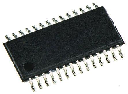
| 描述 | IC REG BUCK SYNC 2.5V 28HTSSOP稳压器—开关式稳压器 Lo-In Vltg 6A Sync Sync Buck Converter |
| 产品分类 | |
| 品牌 | Texas Instruments |
| 产品手册 | |
| 产品图片 |
|
| rohs | 符合RoHS无铅 / 符合限制有害物质指令(RoHS)规范要求 |
| 产品系列 | 电源管理 IC,稳压器—开关式稳压器,Texas Instruments TPS54615PWPSWIFT™ |
| 数据手册 | |
| 产品型号 | TPS54615PWP |
| PWM类型 | 电压模式 |
| 产品培训模块 | http://www.digikey.cn/PTM/IndividualPTM.page?site=cn&lang=zhs&ptm=16804 |
| 产品目录页面 | |
| 产品种类 | 稳压器—开关式稳压器 |
| 供应商器件封装 | 28-HTSSOP |
| 其它名称 | 296-12128-5 |
| 制造商产品页 | http://www.ti.com/general/docs/suppproductinfo.tsp?distId=10&orderablePartNumber=TPS54615PWP |
| 包装 | 管件 |
| 单位重量 | 118.500 mg |
| 同步整流器 | 是 |
| 商标 | Texas Instruments |
| 安装类型 | 表面贴装 |
| 安装风格 | SMD/SMT |
| 宽度 | 4.4 mm |
| 封装 | Tube |
| 封装/外壳 | 28-SOIC(0.173",4.40mm 宽)裸露焊盘 |
| 封装/箱体 | HTSSOP-28 |
| 工作温度 | -40°C ~ 85°C |
| 工作温度范围 | - 40 C to + 85 C |
| 工厂包装数量 | 50 |
| 开关频率 | 700 kHz |
| 拓扑结构 | Buck |
| 最大工作温度 | + 85 C |
| 最大输入电压 | 6 V |
| 最小工作温度 | - 40 C |
| 最小输入电压 | 3 V |
| 标准包装 | 50 |
| 电压-输入 | 3 V ~ 6 V |
| 电压-输出 | 2.5V |
| 电流-输出 | 6A |
| 类型 | 降压(降压) |
| 系列 | TPS54615 |
| 设计资源 | http://www.digikey.com/product-highlights/cn/zh/texas-instruments-webench-design-center/3176 |
| 负载调节 | 0.091 % / A |
| 输入电压 | 3 V to 6 V |
| 输出数 | 1 |
| 输出电压 | 2.5 V |
| 输出电流 | 6 A |
| 输出端数量 | 1 Output |
| 输出类型 | 固定 |
| 配用 | /product-detail/zh/XILINXPWR-082/296-17304-ND/684804 |
| 频率-开关 | 350kHz,550kHz |


- 商务部:美国ITC正式对集成电路等产品启动337调查
- 曝三星4nm工艺存在良率问题 高通将骁龙8 Gen1或转产台积电
- 太阳诱电将投资9.5亿元在常州建新厂生产MLCC 预计2023年完工
- 英特尔发布欧洲新工厂建设计划 深化IDM 2.0 战略
- 台积电先进制程称霸业界 有大客户加持明年业绩稳了
- 达到5530亿美元!SIA预计今年全球半导体销售额将创下新高
- 英特尔拟将自动驾驶子公司Mobileye上市 估值或超500亿美元
- 三星加码芯片和SET,合并消费电子和移动部门,撤换高东真等 CEO
- 三星电子宣布重大人事变动 还合并消费电子和移动部门
- 海关总署:前11个月进口集成电路产品价值2.52万亿元 增长14.8%


PDF Datasheet 数据手册内容提取
Product Sample & Technical Tools & Support & Folder Buy Documents Software Community TPS54611,TPS54612,TPS54613 TPS54614,TPS54615,TPS54616 SLVS400D–AUGUST2001–REVISEDJANUARY2015 TPS5461x 3-V to 6-V Input, 6-A Output Synchronous Buck PWM Switcher With Integrated FETs (SWIFT™) 1 Features 3 Description • 30-mΩ,12-APeakMOSFETSwitchesforHigh The SWIFT™ family of dc/dc regulators, the 1 TPS54611, TPS54612, TPS54613, TPS54614, Efficiencyat6-AContinuousOutputSourceand TPS54615 and TPS54616 low-input voltage high- Sink output current synchronous-buck PWM converters • 0.9-V,1.2-V,1.5-V,1.8-V,2.5-V,and3.3-VFixed integrate all required active components. Included on OutputVoltageDevicesWith1.0%InitialAccuracy the substrate are true, high-performance, voltage • InternallyCompensatedforEasyUseandMinimal error amplifiers that provide high performance under ComponentCount transient conditions; an under-voltage-lockout circuit topreventstart-upuntiltheinputvoltagereaches3V; • FastTransientResponse an internally and externally set slow-start circuit to • WidePWMFrequency− Fixed350kHz,550kHz limit in-rush currents; and a powergood output useful orAdjustable280kHzto700kHz for processor/logic reset, fault signaling, and supply • LoadProtectedbyPeakCurrentLimitand sequencing. ThermalShutdown The TPS5461x devices are available in a thermally • IntegratedSolutionReducesBoardAreaand enhanced 28-pin TSSOP (PWP) PowerPAD™ TotalCost package, which eliminates bulky heatsinks. TI provides evaluation modules and the SWIFT™ 2 Applications designer software tool to aid in quickly achieving high-performance power supply designs to meet • Low-Voltage,High-DensitySystemsWithPower aggressiveequipmentdevelopmentcycles. Distributedat5Vor3.3V • PointofLoadRegulationforHighPerformance DeviceInformation(1) DSPs,FPGAs,ASICsandMicroprocessors PARTNUMBER PACKAGE OUTPUTVOLTAGE • Broadband,NetworkingandOptical TPS54611 0.9V CommunicationsInfrastructure TPS54612 1.2V • PortableComputing/NotebookPCs TPS54613 1.5V HTSSOP(28) TPS54614 1.8V TPS54615 2.5V TPS54616 3.3V (1) For all available packages, see the orderable addendum at theendofthedatasheet. SimplifiedSchematic Efficiencyat350kHz Input Output 100 VIN PH 95 TPS54614 90 BOOT 85 PGND % 80 y - VBIAS VSENSE enc 75 AGND Effici 70 65 60 55 50 0 1 2 3 4 5 6 LoadCurrent-A 1 An IMPORTANT NOTICE at the end of this data sheet addresses availability, warranty, changes, use in safety-critical applications, intellectualpropertymattersandotherimportantdisclaimers.PRODUCTIONDATA.
TPS54611,TPS54612,TPS54613 TPS54614,TPS54615,TPS54616 SLVS400D–AUGUST2001–REVISEDJANUARY2015 www.ti.com Table of Contents 1 Features.................................................................. 1 7.4 DeviceFunctionalModes........................................12 2 Applications........................................................... 1 8 ApplicationandImplementation........................ 13 3 Description............................................................. 1 8.1 ApplicationInformation............................................13 4 RevisionHistory..................................................... 2 8.2 TypicalApplication .................................................13 5 PinConfigurationandFunctions......................... 3 9 PowerSupplyRecommendations...................... 16 6 Specifications......................................................... 4 10 Layout................................................................... 16 6.1 AbsoluteMaximumRatings......................................4 10.1 LayoutGuidelines.................................................16 6.2 RecommendedOperatingConditions.......................4 10.2 LayoutExample....................................................17 6.3 ThermalInformation..................................................4 10.3 ThermalConsiderations........................................17 6.4 DissipationRatings...................................................4 11 DeviceandDocumentationSupport................. 19 6.5 ElectricalCharacteristics...........................................5 11.1 DeviceSupport......................................................19 6.6 TypicalCharacteristics..............................................7 11.2 RelatedLinks........................................................19 7 DetailedDescription.............................................. 9 11.3 Trademarks...........................................................19 7.1 Overview...................................................................9 11.4 Glossary................................................................19 7.2 FunctionalBlockDiagram.........................................9 12 Mechanical,Packaging,andOrderable Information........................................................... 19 7.3 FeatureDescription...................................................9 4 Revision History ChangesfromRevisionC(April2005)toRevisionD Page • AddedFeatureDescriptionsection,DeviceFunctionalModes,ApplicationandImplementationsection,Power SupplyRecommendationssection,Layoutsection,DeviceandDocumentationSupportsection,andMechanical, Packaging,andOrderableInformationsection. .................................................................................................................... 1 2 SubmitDocumentationFeedback Copyright©2001–2015,TexasInstrumentsIncorporated ProductFolderLinks:TPS54611 TPS54612 TPS54613TPS54614 TPS54615 TPS54616
TPS54611,TPS54612,TPS54613 TPS54614,TPS54615,TPS54616 www.ti.com SLVS400D–AUGUST2001–REVISEDJANUARY2015 5 Pin Configuration and Functions TPS5461xPWPPackage 28-PinHTSSOP TopView AGND 1 28 RT VSENSE 2 27 FSEL NC 3 26 SS/ENA PWRGD 4 25 VBIAS BOOT 5 24 VIN PH 6 23 VIN PH 7 THERMAL 22 VIN PH 8 PAD 21 VIN PH 9 20 VIN PH 10 19 PGND PH 11 18 PGND PH 12 17 PGND PH 13 16 PGND PH 14 15 PGND PinFunctions PIN TYPE(1) DESCRIPTION NAME NO. AGND 1 G Analogground.Returnforslow-startcapacitor,VBIAScapacitor,RTresistorFSEL.MakePowerPAD connectiontoAGND. BOOT 5 S Bootstrapinput.0.022-µFto0.1-µFlow-ESRcapacitorconnectedfromBOOTtoPHgeneratesfloating driveforthehigh-setFETdriver. FSEL 27 I Frequencyselectinput.Provideslogicinputtoselectbetweentwointernallysetswitchingfrequencies. NC 3 – Noconnection PGND 15−19 G Powerground.Highcurrentreturnforthelow-sidedriverandpowerMOSFET.ConnectPGNDwithlarge copperareastotheinputandoutputsupplyreturns,andnegativeterminalsoftheinputandoutput capacitors. PH 6−14 O Phaseinput/output.Junctionoftheinternalhigh-sideandlow-sidepowerMOSFETs,andoutputinductor. PWRGD 4 O Powergoodopen-drainoutput.High-ZwhenVSENSE≥90%Vref,otherwisePWRGDislow.Notethat outputislowwhenSS/ENAisloworinternalshutdownsignalactive. RT 28 I Frequencysettingresistorinput.ConnectaresistorfromRTtoAGNDtosettheswitchingfrequency. SS/ENA 26 I Slow-start/enableinput/output.Dualfunctionpinwhichprovideslogicinputtoenable/disabledevice operationandcapacitorinputtoexternallysetthestart-uptime. VBIAS 25 S Internalbiasregulatoroutput.Suppliesregulatedvoltagetointernalcircuitry.BypassVBIASpintoAGND pinwithahighquality,low-ESR0.1-µFto1-µFceramiccapacitor. VIN 20−24 I InputsupplyforthepowerMOSFETswitchesandinternalbiasregulator.BypassVINpinstoPGNDpins closetodevicepackagewithahighquality,low-ESR1-µFto10-µFceramiccapacitor. VSENSE 2 I Erroramplifierinvertinginput.Connectdirectlytooutputvoltagesensepoint. (1) I=Input,O=Output,S=Supply,G=Ground Copyright©2001–2015,TexasInstrumentsIncorporated SubmitDocumentationFeedback 3 ProductFolderLinks:TPS54611 TPS54612 TPS54613TPS54614 TPS54615 TPS54616
TPS54611,TPS54612,TPS54613 TPS54614,TPS54615,TPS54616 SLVS400D–AUGUST2001–REVISEDJANUARY2015 www.ti.com 6 Specifications 6.1 Absolute Maximum Ratings overoperatingfree-airtemperaturerange(unlessotherwisenoted)(1) MIN MAX UNIT VIN,SS/ENA,FSEL −0.3 7 V RT −0.3 6 V V Inputvoltage I VSENSE −0.3 4 V BOOT −0.3 17 V VBIAS,PWRGD −0.3 7 V V Outputvoltage O PH −0.6 10 V PH InternallyLimited V I Sourcecurrent O VBIAS 6 mA PH 12 A I Sinkcurrent S SS/ENA,PWRGD 10 mA Voltagedifferential AGNDtoPGND –0.3 0.3 V Continuouspowerdissipation SeeThermalInformation T Operatingvirtualjunctiontemperature –40 125 °C J T Storagetemperature −65 150 °C stg (1) StressesbeyondthoselistedunderAbsoluteMaximumRatingsmaycausepermanentdamagetothedevice.Thesearestressratings only,whichdonotimplyfunctionaloperationofthedeviceattheseoranyotherconditionsbeyondthoseindicatedunderRecommended OperatingConditions.Exposuretoabsolute-maximum-ratedconditionsforextendedperiodsmayaffectdevicereliability. 6.2 Recommended Operating Conditions overoperatingfree-airtemperaturerange(unlessotherwisenoted) MIN NOM MAX UNIT ControllerInputVoltage,V 3 6 V IN JunctionTemperature,T –40 125 °C J 6.3 Thermal Information(1) TPS5461x THERMALMETRIC(2) UNIT PWP(28PINS) R Junction-to-ambientthermalresistance,withsolder 18.2 θJA °C/W Junction-to-ambientthermalresistance,withoutsolder 40.5 (1) TestBoardConditions: (a)3inches×3inches,4layers,thickness:0.062inch (b)1.5oz.coppertraceslocatedonthetopofthePCB (c)1.5oz.coppergroundplaneonthebottomofthePCB (d)0.5oz.coppergroundplanesonthe2internallayers (e)12thermalvias.SeeFigure19formoreinformation. (2) Formoreinformationabouttraditionalandnewthermalmetrics,seetheICPackageThermalMetricsapplicationreport,SPRA953. 6.4 Dissipation Ratings(1)(2) TA=25°C TA=70°C TA=85°C UNIT POWERRATING POWERRATING POWERRATING 28PinPWPwithSolder 5.49 (3) 3.02 2.20 W (1) FormoreinformationonthePWPpackage,refertoTItechnicalbrief,SLMA002 (2) TestBoardConditions: (a)3inches×3inches,4layers,thickness:0.062inch (b)1.5oz.coppertraceslocatedonthetopofthePCB (c)1.5oz.coppergroundplaneonthebottomofthePCB (d)0.5oz.coppergroundplanesonthe2internallayers (e)12thermalvias.SeeFigure19formoreinformation. (3) Maximumpowerdissipationmaybelimitedbyover-currentprotection 4 SubmitDocumentationFeedback Copyright©2001–2015,TexasInstrumentsIncorporated ProductFolderLinks:TPS54611 TPS54612 TPS54613TPS54614 TPS54615 TPS54616
TPS54611,TPS54612,TPS54613 TPS54614,TPS54615,TPS54616 www.ti.com SLVS400D–AUGUST2001–REVISEDJANUARY2015 Dissipation Ratings(1)(2) (continued) TA=25°C TA=70°C TA=85°C UNIT POWERRATING POWERRATING POWERRATING 28PinPWPwithoutSolder 2.48 1.36 0.99 W 6.5 Electrical Characteristics T =–40°Cto125°C,V =3Vto6V(unlessotherwisenoted) J I PARAMETER TESTCONDITIONS MIN TYP MAX UNIT SUPPLYVOLTAGE,VIN V Inputvoltagerange 3.0 6.0 V IN f =350kHz,FSEL≤0.8V,RTopen,phasepinopen 6.2 9.6 s I Quiescentcurrent =550kHz,FSEL≤2.5V,RTopen,phasepinopen 8.4 12.8 mA (Q) fs Shutdown,SS/ENA=0V 1 1.4 UNDERVOLTAGELOCKOUT Startthresholdvoltage 2.95 3.0 V Stopthresholdvoltage 2.70 2.80 V UVLO Hysteresisvoltage 0.14 0.16 V Risingandfallingedgedeglitch(1) 2.5 µs BIASVOLTAGE Outputvoltage I =0 2.70 2.80 2.90 V (VBIAS) VBIAS Outputcurrent(2) 100 µA OUTPUTVOLTAGE T =25°C,VIN=5V 0.9 J TPS54611 V 3V≤VIN≤6V,0≤I ≤6A,−40°C≤T ≤125°C –2.0% 2.0% L J T =25°C,VIN=5V 1.2 J TPS54612 V 3V≤VIN≤6V,0≤I ≤6A,−40°C≤T ≤125°C –2.0% 2.0% L J T =25°C,VIN=5V 1.5 J TPS54613 V 3V≤VIN≤6V,0≤I ≤6A,−40°C≤T ≤125°C –2.0% 2.0% L J V Outputvoltage O T =25°C,VIN=5V 1.8 J TPS54614 V 3V≤VIN≤6V,0≤I ≤6A,−40°C≤T ≤125°C –3.0% 3.0% L J T =25°C,VIN=5V 2.5 J TPS54615 V 3V≤VIN≤6V,0≤I ≤6A,−40°≤T ≤125°C –3.0% 3.0% L J T =25°C,VIN=5V 3.3 J TPS54616 V 4V≤VIN≤6V,0≤I ≤6A,−40°≤T ≤125°C −3.0% 3.0% L J REGULATION Lineregulation(1)(3) I =3A,350≤f ≤550kHz,T =85°C 0.088 %/V L s J Loadregulation(1)(3) I =0Ato6A,350≤f ≤550kHz,T =85°C 0.0917 %/A L s J OSCILLATOR Internallyset–freerunning FSEL≤0.8V,RTopen 280 350 420 kHz frequency FSEL≥2.5V,RTopen 440 550 660 RT=180kΩ(1%resistortoAGND)(1) 252 280 308 Externallyset–freerunning RT=100kΩ(1%resistortoAGND) 460 500 540 kHz frequencyrange RT=68kΩ(1%resistortoAGND)(1) 663 700 762 Highlevelthreshold 2.5 V FSEL Lowlevelthreshold 0.8 V Rampvalley(1) 0.75 V Rampamplitude(peak-to-peak)(1) 1 V (1) Specifiedbydesign (2) Staticresistiveloadsonly (3) TestedusingcircuitinFigure10. Copyright©2001–2015,TexasInstrumentsIncorporated SubmitDocumentationFeedback 5 ProductFolderLinks:TPS54611 TPS54612 TPS54613TPS54614 TPS54615 TPS54616
TPS54611,TPS54612,TPS54613 TPS54614,TPS54615,TPS54616 SLVS400D–AUGUST2001–REVISEDJANUARY2015 www.ti.com Electrical Characteristics (continued) T =–40°Cto125°C,V =3Vto6V(unlessotherwisenoted) J I PARAMETER TESTCONDITIONS MIN TYP MAX UNIT Minimumcontrollableontime(1) 200 ns Maximumdutycycle(1) 90% ERRORAMPLIFIER Erroramplifieropenloopvoltage gain(1) 26 dB Erroramplifierunitygain bandwidth(1) 3 5 MHz Erroramplifiercommonmodeinput PoweredbyinternalLDO(1) 0 VBIAS V voltagerange PWMCOMPARATOR PWMcomparatorpropagationdelay time,PWMcomparatorinputtoPH 10-mVoverdrive(1) 70 85 ns pin(excludingdeadtime) SLOW-START/ENABLE Enablethresholdvoltage,SS/ENA 0.82 1.20 1.40 V Enablehysteresisvoltage, SS/ENA(1) 0.03 V Fallingedgedeglitch,SS/ENA(1) 2.5 µs TPS54611 2.6 3.3 4.1 TPS54612 3.5 4.5 5.4 Internalslow-start TPS54613 4.4 5.6 6.7 time(1) TPS54614 2.6 3.3 4.1 ms TPS54615 3.6 4.7 5.6 TPS54616 4.7 6.1 7.6 Chargecurrent,SS/ENA SS/ENA=0V 3 5 8 µA Dischargecurrent,SS/ENA SS/ENA=0.2V,V =2.7V 1.5 2.3 4.0 mA I POWERGOOD Powergoodthresholdvoltage VSENSEfalling 90 %V O Powergoodhysteresisvoltage See (1) 3 %V O Powergoodfallingedgedeglitch See (1) 35 µs Outputsaturationvoltage,PWRGD I =2.5mA 0.18 0.3 V (sink) Leakagecurrent,PWRGD V =5.5V 1 µA I CURRENTLIMIT V =3V(1) 7.2 10 I Currentlimit A V =6V(1) 10 12 I Currentlimitleadingedgeblanking time(1) 100 ns Currentlimittotalresponsetime(1) 200 ns THERMALSHUTDOWN Thermalshutdowntrippoint(1) 135 150 165 °C Thermalshutdownhysteresis(1) 10 OUTPUTPOWERMOSFETS I =3A,V =6V(4) 26 47 O I r PowerMOSFETswitches mΩ DS(on) I =3A,V =3V(4) 36 65 O I (4) MatchedMOSFETs,low-sider productiontested,high-sider specifiedbydesign. DS(on) DS(on) 6 SubmitDocumentationFeedback Copyright©2001–2015,TexasInstrumentsIncorporated ProductFolderLinks:TPS54611 TPS54612 TPS54613TPS54614 TPS54615 TPS54616
TPS54611,TPS54612,TPS54613 TPS54614,TPS54615,TPS54616 www.ti.com SLVS400D–AUGUST2001–REVISEDJANUARY2015 6.6 Typical Characteristics 120 100 Ω− VI=3.3V Ω− VI=5V Resistance 10800 IO=3A Resistance 6800 IO=3A On-State 60 On-State 40 Drain-Source 2400 Drain-Source 20 0 0 −40 0 25 85 125 −40 0 25 85 125 TJ−JunctionTemperature−°C TJ−JunctionTemperature−°C Figure1.Drain-sourceOn-stateResistancevsJunction Figure2.Drain-sourceOn-stateResistancevsJunction Temperature Temperature2 800 Hz Hz RT=68k uency - k 650 FSEL≥2.5V uency - k 700 q q or Fre 550 or Fre 600 RT=100k Set Oscillat 450 FSEL≤0.8V Set Oscillat 450000 nally 350 nally 300 RT= 180 k f - Inter 250−40 0 25 85 125 f - Exter 200−40 0 25 85 125 TJ−JunctionTemperature−°C TJ−JunctionTemperature−°C Figure3.InternallySetOscillatorFrequencyvsJunction Figure4.ExternallySetOscillatorFrequencyvsJunction Temperature3 Temperature4 0.895 0.8950 TA=85°C V V 0.893 −n 0.8930 nce- ulatio Refere 0.891 ge Reg 0.8910 e a Voltag 0.889 oltut V 0.8890 f=350kHz V−ref0.887 −Outp 0.8870 O V 0.885 0.8850 −40 0 25 85 125 3 4 5 6 TJ−JunctionTemperature−°C VI−InputVoltage−V TestedusingTPS54611 Figure5.VoltageReferencevsJunctionTemperature Figure6.OutputVoltageRegulationvsInputVoltage Copyright©2001–2015,TexasInstrumentsIncorporated SubmitDocumentationFeedback 7 ProductFolderLinks:TPS54611 TPS54612 TPS54613TPS54614 TPS54615 TPS54616
TPS54611,TPS54612,TPS54613 TPS54614,TPS54615,TPS54616 SLVS400D–AUGUST2001–REVISEDJANUARY2015 www.ti.com Typical Characteristics (continued) 140 0 3.80 RL=10kΩ, −20 120 CL=160pF, s3.65 TA=25°C −40 m Ga−dinB1068000 Phase −−−6810000 Deg−rees w-Start Time−33..3505 4200 Gain −−−111246000 Phase nternal Slo33..2050 I 0 −180 2.90 −20 −200 2.75 0 10 100 1k 10k 100k 1M 10M −40 0 25 85 125 f−Frequency−Hz TJ−JunctionTemperature−°C TestedusingTPS54611 Figure7.ErrorAmplifierOpenLoopResponse Figure8.InternalSlow-StartTimevsJunctionTemperature 5 4.5 TJ=125°C FS=700kHz W 4 s− 3.5 VI=3.3V e ss 3 o L er 2.5 w Po 2 e evic 1.5 VI=5.0V D 1 0.5 0 0 1 2 3 4 5 6 7 8 IL−Load Current−A Figure9.DevicePowerLossesvsLoadCurrent 8 SubmitDocumentationFeedback Copyright©2001–2015,TexasInstrumentsIncorporated ProductFolderLinks:TPS54611 TPS54612 TPS54613TPS54614 TPS54615 TPS54616
TPS54611,TPS54612,TPS54613 TPS54614,TPS54615,TPS54616 www.ti.com SLVS400D–AUGUST2001–REVISEDJANUARY2015 7 Detailed Description 7.1 Overview The SWIFT family of DC - DC regulators, the TPS54611, TPS54612, TPS54613, TPS54614, TPS54615, and TPS54616 are low-input voltage high-output current synchronous-buck PWM converters integrate all required active components. Included on the substrate are true, high-performance, voltage error amplifiers that provide high performance under transient conditions; an under-voltage-lockout circuit to prevent start-up until the input voltage reaches 3 V; an internally and externally set slow-start circuit to limit in-rush currents; and a powergood outputusefulforprocessor/logicreset,faultsignaling,andsupplysequencing. 7.2 Functional Block Diagram AGND VBIAS VIN Enable 5 µAComparator SS/ENA VBIAS REG Falling SHUTDOWN 1.8V Edge ILIM VIN Deglitch Thermal Comparator VIN Hysteresis:0.03 2.5 µs Shutdown Leading V 145°C Edge VINUVLO Blanking Comparator Falling 100ns and VIN Rising BOOT 2.94V Edge Sensefet Hysteresis:0.16 Deglitch 30mΩ V 2.5 µs SS_DIS SHUTDOWN Internal/External PH LOUT VO Slow-Start (Internal Slow-StartTime + R Q AdaptiveDead-Time CO = − and 3.3 ms to 6.6 ms) 2kΩ S ControlLogic 40kΩ PWM Error Comparator 25nsAdaptive VIN VI Amplifier Deadtime 30mΩ VI Feed-Forward Compensation OSC PGND Powergood Comparator Reference/ DAC Falling PWRGD VSENSE Edge 0.90Vref Deglitch TPS5461x Hysteresis:0.03Vref SHUTDOWN 35 µs VSENSE RT FSEL 7.3 Feature Description 7.3.1 UndervoltageLockOut(UVLO) The TPS5461x incorporates an UVLO circuit to keep the device disabled when the input voltage (VIN) is insufficient. During power up, internal circuits are held inactive until VIN exceeds the nominal UVLO threshold voltage of 2.95 V. Once the UVLO start threshold is reached, device start-up begins. The device operates until VIN falls below the nominal UVLO stop threshold of 2.8 V. Hysteresis in the UVLO comparator, and a 2.5-µs risingandfallingedgedeglitchcircuit,reducesthelikelihoodofshuttingthedevicedownduetonoiseonVIN. Copyright©2001–2015,TexasInstrumentsIncorporated SubmitDocumentationFeedback 9 ProductFolderLinks:TPS54611 TPS54612 TPS54613TPS54614 TPS54615 TPS54616
TPS54611,TPS54612,TPS54613 TPS54614,TPS54615,TPS54616 SLVS400D–AUGUST2001–REVISEDJANUARY2015 www.ti.com Feature Description (continued) 7.3.2 Slow-StartandEnable(SS/ENA) The slow-start/enable pin provides two functions. First, the pin acts as an enable (shutdown) control by keeping the device turned off until the voltage exceeds the start threshold voltage of approximately 1.2 V. When SS/ENA exceeds the enable threshold, device start up begins. The reference voltage fed to the error amplifier is linearly ramped up from 0 V to 0.891 V in 3.35 ms. Similarly, the converter output voltage reaches regulation in approximately 3.35 ms. Voltage hysteresis and a 2.5-µs falling edge deglitch circuit reduce the likelihood of triggeringtheenableduetonoise.RefertoTable1forstartuptimesforeachdevice. Table1.DeviceStartupTimes DEVICE OUTPUTVOLTAGE SLOW-START TPS54611 0.9V 3.3ms TPS54612 1.2V 4.5ms TPS54613 1.5V 5.6ms TPS54614 1.8V 3.3ms TPS54615 2.5V 4.7ms TPS54616 3.3V 6.1ms The second function of the SS/ENA pin provides an external means for extending the slow-start time with a ceramiccapacitorconnectedbetweenSS/ENAandAGND.AddingacapacitortotheSS/ENApinhastwoeffects on start-up. First, a delay occurs between release of the SS/ENA pin and start-up of the output. The delay is proportional to the slow-start capacitor value and lasts until the SS/ENA pin reaches the enable threshold. The start-updelayisapproximately: 1.2 V t =C ´ d (SS) 5 mA (1) Second,astheoutputbecomesactive,abrieframpupattheinternalslow-startratemaybeobservedbeforethe externally set slow-start rate takes control and the output rises at a rate proportional to the slow-start capacitor. Theslow-starttimesetbythecapacitorisapproximately: 0.7 V t =C ´ (SS) (SS) 5 mA (2) The actual slow-start time is likely to be less than the above approximation due to the brief ramp up at the internalrate 7.3.3 VBIASRegulator The VBIAS regulator provides internal analog and digital blocks with a stable supply voltage over variations in junction temperature and input voltage. A high quality, low-ESR, ceramic bypass capacitor is required on the VBIAS pin. X7R or X5R grade dielectrics are recommended because their values are more stable over temperature.ThebypasscapacitorshouldbeplacedclosetotheVBIASpinandreturnedtoAGND. External loading on VBIAS is allowed, with the caution that internal circuits require a minimum VBIAS of 2.7 V, andexternalloadsonVBIASwithacordigitalswitchingnoisemaydegradeperformance.TheVBIASpinmaybe usefulasareferencevoltageforexternalcircuits. 7.3.4 VoltageReference The voltage reference system produces a precise, temperature-stable voltage from a bandgap circuit. A scaling amplifierandDACarethenusedtoproducethereferencevoltagesforeachofthefixedoutputdevices. 7.3.5 OscillatorandPWMRamp The oscillator frequency can be set to internally fixed values of 350 kHz or 550 kHz using the FSEL pin as a static digital input. If a different frequency of operation is required for the application, the oscillator frequency can be externally adjusted from 280 kHz to 700 kHz by connecting a resistor from the RT pin to AGND and floating the FSEL pin. The switching frequency is approximated by the following equation, where R is the resistance from RTtoAGND 10 SubmitDocumentationFeedback Copyright©2001–2015,TexasInstrumentsIncorporated ProductFolderLinks:TPS54611 TPS54612 TPS54613TPS54614 TPS54615 TPS54616
TPS54611,TPS54612,TPS54613 TPS54614,TPS54615,TPS54616 www.ti.com SLVS400D–AUGUST2001–REVISEDJANUARY2015 100 kW SwitchingFrequency = ´500 [kHz] R (3) Table2summarizesthefrequencyselectionconfigurations: Table2.SwitchingFrequencies SWITCHINGFREQUENCY SYNCPIN RTPIN 350kHz,internallyset FloatorAGND Float 550kHz,internallyset ≥2.5V Float Externallyset280kHzto700kHz Float R=180kto68k 7.3.6 ErrorAmplifier The high performance, wide bandwidth, voltage error amplifier is gain-limited to provide internal compensation of the control loop. The user is given limited flexibility in choosing output L and C filter components. Inductance values of 4.7 µH to 10 µH are typical and available from several vendors. The resulting designs exhibit good noise and ripple characteristics, but with exceptional transient response. Transient recovery times are typically in therangeof10µsto20 µs. 7.3.7 PWMControl Signalsfromtheerroramplifieroutput,oscillator,andcurrentlimitcircuitareprocessedbythePWMcontrollogic. Referring to the internal block diagram, the control logic includes the PWM comparator, OR gate, PWM latch, and portions of the adaptive dead-time and control logic block. During steady-state operation below the current limit threshold, the PWM comparator output and oscillator pulse train alternately set and reset the PWM latch. Once the PWM latch is set, the low-side FET remains on for a minimum duration set by the oscillator pulse width. During this period, the PWM ramp discharges rapidly to its valley voltage. When the ramp begins to charge back up, the low-side FET turns off and high-side FET turns on. As the PWM ramp voltage exceeds the error amplifier output voltage, the PWM comparator resets the latch, thus turning off the high-side FET and turning on the low-side FET. The low-side FET remains on until the next oscillator pulse discharges the PWM ramp. During transient conditions, the error amplifier output could be below the PWM ramp valley voltage or above the PWM peak voltage. If the error amplifier is high, the PWM latch is never reset, and the high-side FET remains on until the oscillator pulse signals the control logic to turn the high-side FET off and the low-side FET on. The device operates at its maximum duty cycle until the output voltage rises to the regulation set-point, setting VSENSE to approximately the same voltage as V . If the error amplifier output is low, the PWM latch is ref continually reset and the high-side FET does not turn on. The low-side FET remains on until the VSENSE voltage decreases to a range that allows the PWM comparator to change states. The TPS5461x devices are capableofsinkingcurrentcontinuouslyuntiltheoutputreachestheregulationset-point. If the current limit comparator trips for longer than 100 ns, the PWM latch resets before the PWM ramp exceeds the error amplifier output. The high-side FET turns off and the low-side FET turns on to decrease the energy in the output inductor and consequently decrease the output current. This process is repeated each cycle in which thecurrentlimitcomparatoristripped. 7.3.8 Dead-TimeControlandMOSFETDrivers Adaptive dead-time control prevents shoot-through current from flowing in both N-channel power MOSFETs during the switching transitions by actively controlling the turnon times of the MOSFET drivers. The high-side driver does not turn on until the voltage at the gate of the low-side FET is below 2 V. The high-side and low-side drivers are designed with 300 mA source and sink capability to quickly drive the power MOSFETs gates. The low-side driver is supplied from VIN, while the high-side drive is supplied from the BOOT pin. A bootstrap circuit uses an external BOOT capacitor and internal 2.5-Ω bootstrap switch connected between the VIN and BOOT pins.Theintegratedbootstrapswitchimprovesdriveefficiencyandreducesexternalcomponentcount. Copyright©2001–2015,TexasInstrumentsIncorporated SubmitDocumentationFeedback 11 ProductFolderLinks:TPS54611 TPS54612 TPS54613TPS54614 TPS54615 TPS54616
TPS54611,TPS54612,TPS54613 TPS54614,TPS54615,TPS54616 SLVS400D–AUGUST2001–REVISEDJANUARY2015 www.ti.com 7.3.9 OvercurrentProtection Cycle-by-cycle current limiting is achieved by sensing the current flow through the high-side MOSFET and a differential amplifier with preset overcurrent threshold. The high-side MOSFET is turned off within 200 ns of reaching the current limit threshold. A 100 ns leading edge blanking circuit prevents false tripping of current limit. Current limit detection occurs only when current flows from VIN to PH when sourcing current to the output filter. Loadprotectionduringcurrentsinkoperationisprovidedbythermalshutdown. 7.3.10 ThermalShutdown The device uses the thermal shutdown to turn off the power MOSFETs and disable the controller if the junction temperature exceeds 150°C. The device is released from shutdown when the junction temperature decreases to 10°C below the thermal shutdown trip point, and starts up under control of the slow-start circuit. Thermal shutdown provides protection when an overload condition is sustained for several milliseconds. With a persistent fault condition, the device cycles continuously: starting up by control of the slow-start circuit, heating up due to thefault,andthenshuttingdownuponreachingthethermalshutdowntrippoint. 7.3.11 Powergood(PWRGD) The powergood circuit monitors for undervoltage conditions on VSENSE. If the voltage on VSENSE falls 10% below the reference voltage, the open-drain PWRGD output is pulled low. PWRGD is also pulled low if VIN is less than the UVLO threshold, or SS/ENA is low, or thermal shutdown is asserted. When VIN = UVLO threshold, SS/ENA = enable threshold, and VSENSE > 90% of V , the open-drain output of the PWRGD pin is high. A ref hysteresis voltage equal to 3% of V and a 35-µs falling edge deglitch circuit prevent tripping of the powergood ref comparatorduetohigh-frequencynoise. 7.4 Device Functional Modes 7.4.1 ContinuousConductionMode These devices operate in continuous conduction mode (CCM) at a fixed frequency regardless of the output current. 12 SubmitDocumentationFeedback Copyright©2001–2015,TexasInstrumentsIncorporated ProductFolderLinks:TPS54611 TPS54612 TPS54613TPS54614 TPS54615 TPS54616
TPS54611,TPS54612,TPS54613 TPS54614,TPS54615,TPS54616 www.ti.com SLVS400D–AUGUST2001–REVISEDJANUARY2015 8 Application and Implementation NOTE Information in the following applications sections is not part of the TI component specification, and TI does not warrant its accuracy or completeness. TI’s customers are responsible for determining suitability of components for their purposes. Customers should validateandtesttheirdesignimplementationtoconfirmsystemfunctionality. 8.1 Application Information The TPS5461x devices are fixed output voltage synchronous step-down DC-DC converters. These devices are usedtoconvertahigherDCinputvoltagetoalowerDCoutputvoltagewithamaximumoutputcurrentof6A. 8.2 Typical Application Figure 10 shows the schematic diagram for a typical TPS54614 application. The TPS54614 (U1) can provide greater than 6 A of output current at a nominal output voltage of 1.8 V. For proper operation, the exposed thermalPowerPADunderneaththeintegratedcircuitpackageneedstobesolderedtotheprinted-circuitboard. VI 20 VIN BOOT 5 3 V−6 V 220µF 10µF 21 VIN PH 6 0.047µF 22 7 VIN PH 23 8 7.2µH VIN PH V 24 9 O VIN PH 1.8 V 10 kΩ PH 10 680µF 27 11 FSEL PH PwrGood 28 12 RT PH 26 13 SS/ENA PH 25 14 VBIAS PH 4 15 PWRGD PGND Enable 3 16 NC PGND 0.1µF 2 17 VSENSE PGND CSS 18 PGND 1 19 AGND PGND PwrPad Figure10. ApplicationCircuit 8.2.1 DesignRequirements ThedesignrequirementsforthisexamplearelistedinTable3. Table3.DesignParameters DESIGNPARAMETER EXAMPLEVALUE DCInputVoltageRange 3V–6V DCOutputVoltage 1V DCOutputCurrentRange 0A–6A LoadTransientStep 3A–6A LoadRegulationControl ±5mV LoopCrossoverFrequency 50kHz ControlLoopPhaseMargin 55° Copyright©2001–2015,TexasInstrumentsIncorporated SubmitDocumentationFeedback 13 ProductFolderLinks:TPS54611 TPS54612 TPS54613TPS54614 TPS54615 TPS54616
TPS54611,TPS54612,TPS54613 TPS54614,TPS54615,TPS54616 SLVS400D–AUGUST2001–REVISEDJANUARY2015 www.ti.com 8.2.2 DetailedDesignProcedure 8.2.2.1 ComponentSelection The values for the components used in this design example were selected using the SWIFT designer software tool. SWIFT designer provides a complete design environment for developing dc-dc converters using the TPS54614, or other devices in the SWIFT product family. Additional design information is available at www.ti.com. 8.2.2.2 InputFilter The input to the circuit is a nominal 3.3 VDC or 5 VDC. The input filter is a 220-μF POSCAP capacitor, with a maximum allowable ripple current of 3 A. A 10-µF ceramic capacitor for the TPS54614 is required, and must be locatedascloseaspossibletothedevice. 8.2.2.3 FeedbackCircuit The output voltage of the converter is fed directly into the VSENSE pin of the TPS54614. The TPS54614 is internallycompensatedtoprovidestabilityoftheoutputundervaryinglineandloadconditions. 8.2.2.4 OperatingFrequency In the application circuit, 350 kHz operation is selected by leaving FSEL open. Different operating frequencies canbeselectedbyconnectingaresistorbetweenRTpinandAGND.ChoosethevalueofRusingEquation4 for thedesiredoperatingfrequency: 500 kHz R= ´100 kW SwitchingFrequency (4) Alternately, a preset operating frequency of 550 kHz can be selected by leaving RT open and connecting the FSELpintoV. I 8.2.2.5 OutputFilter The output filter is composed of a 5.2-µH inductor and a 470-µF capacitor. The inductor is low dc resistance (16- mΩ) type, Sumida CDRH104R−5R2. The capacitor used is a 4-V POSCAP with a maximum ESR of 40 mΩ. The output filter components work with the internal compensation network to provide a stable closed loop response fortheconverter. 8.2.3 ApplicationCurves 100 1.03 1.02 90 VI=5V −V −%ency VI=3.3V ut Voltage 1.011 VI=5V Effici 70 Outp 0.99 VI=3.3V − O V 60 0.98 50 0.97 0 1 2 3 4 5 6 7 8 9 10 0 1 2 3 4 5 6 7 8 9 10 IL−Load Current−A IL−Load Current−A Figure11.EfficiencyvsLoadCurrent Figure12.OutputVoltagevsLoadCurrent 14 SubmitDocumentationFeedback Copyright©2001–2015,TexasInstrumentsIncorporated ProductFolderLinks:TPS54611 TPS54612 TPS54613TPS54614 TPS54615 TPS54616
TPS54611,TPS54612,TPS54613 TPS54614,TPS54615,TPS54616 www.ti.com SLVS400D–AUGUST2001–REVISEDJANUARY2015 60 180 400 16 50 350 14 40 Phase 135 mV 300 12A Gain−dB 213000 Gain 90 hase−Degrees Output−Voltage 221505000 6810Output− Current 0 45 P −O100 4 −O V I −10 50 2 −20 0 0 0 10 100 1k 10k 100k 0 20 40 60 80 100120140160180200 f−Frequency−Hz t−Time−µs Figure13.LoopResponse Figure14.TransientResponse 8 80 7 70 6 mV 60 V − −oltage 54 Voltage 5400 InputV 3 Output 30 −VI 2 −VO 20 1 10 0 0 0 2 4 6 8 10 12 14 16 18 20 0 20 40 60 80 100120140160180200 t−Time−µs t−Time−µs Figure15.Start-upWaveforms Figure16.OutputRippleVoltage 125 TJ=125°C 115 FS=700kHz C °−e 105 VI=5V ur 95 at er 85 p m Te 75 bient 65 VI=3.3V m 55 A −A 45 SafeOperatingArea T 35 25 0 1 2 3 4 5 6 7 8 IL−Load Current−A Figure17.AmbientTemperaturevsLoadCurrent Copyright©2001–2015,TexasInstrumentsIncorporated SubmitDocumentationFeedback 15 ProductFolderLinks:TPS54611 TPS54612 TPS54613TPS54614 TPS54615 TPS54616
TPS54611,TPS54612,TPS54613 TPS54614,TPS54615,TPS54616 SLVS400D–AUGUST2001–REVISEDJANUARY2015 www.ti.com 9 Power Supply Recommendations These devices operate from an input supply voltage between 3 V and 6 V. This supply must be well-regulated. Properbypassingofinputsuppliesandinternalregulatorsiscriticalfornoiseperformance,asisgoodPCBlayout practice.SeetherecommendationsinLayout. 10 Layout 10.1 Layout Guidelines Figure18showsageneralizedPCBlayoutguidefortheTPS5461x. • The VIN pins should be connected together on the printed circuit board (PCB) and bypassed with a low ESR ceramic bypass capacitor. Care should be taken to minimize the loop area formed by the bypass capacitor connections, the VIN pins, and the TPS54311−16 ground pins. The minimum recommended bypass capacitance is 10-μF ceramic with a X5R or X7R dielectric and the optimum placement is closest to the VIN pinsandthePGNDpins. • The TPS54311−16 has two internal grounds (analog and power). Inside the TPS54311−16, the analog ground ties to all of the noise sensitive signals, while the power ground ties to the noisier power signals. Noise injected between the two grounds can degrade the performance of the TPS54311−16, particularly at higher output currents. Ground noise on an analog ground plane can also cause problems with some of the control and bias signals. For these reasons, separate analog and power ground traces are recommended. There should be an area of ground one the top layer directly under the IC, with an exposed area for connection to the PowerPAD. Use vias to connect this ground area to any internal ground planes. Use additional vias at the ground side of the input and output filter capacitors as well. The AGND and PGND pins should be tied to the PCB ground by connecting them to the ground area under the device as shown. The only components that should tie directly to the power ground plane are the input capacitors, the output capacitors, the input voltage decoupling capacitor, and the PGND pins of the TPS54311−16. Use a separate wide trace for the analog ground signal path. This analog ground should be used for the timing resistor RT, slowstartcapacitorandbiascapacitorgrounds.ConnectthistracedirectlytoAGND(pin1). • The PH pins should be tied together and routed to the output inductor. Since the PH connection is the switching node, inductor should be located very close to the PH pins and the area of the PCB conductor minimizedtopreventexcessivecapacitivecoupling. • Connect the boot capacitor between the phase node and the BOOT pin as shown. Keep the boot capacitor closetotheICandminimizetheconductortracelengths. • Connect the output filter capacitor(s) as shown between the VOUT trace and PGND. It is important to keep theloopformedbythePHpins,Lout,CoutandPGNDassmallaspractical. • ConnecttheoutputofthecircuitdirectlytotheVSENSEpin.DonotplacethistracetooclosetothePHtrace. Do to the size of the IC package and the device pinout, they will have to be routed somewhat close, but maintainasmuchseparationaspossiblewhilestillkeepingthelayoutcompact. • Connect the bias capacitor from the VBIAS pin to analog ground using the isolated analog ground trace. If a slow-start capacitor or RT resistor is used, or if the SYNC pin is used to select 350-kHz operating frequency, connectthemtothistraceaswell. 16 SubmitDocumentationFeedback Copyright©2001–2015,TexasInstrumentsIncorporated ProductFolderLinks:TPS54611 TPS54612 TPS54613TPS54614 TPS54615 TPS54616
TPS54611,TPS54612,TPS54613 TPS54614,TPS54615,TPS54616 www.ti.com SLVS400D–AUGUST2001–REVISEDJANUARY2015 10.2 Layout Example ANALOG GROUNDTRACE FREQUENCYSETRESISTOR AGND RT VSENSE FSEL SLOWSTART CAPACITOR NC SS/ENA BIASCAPACITOR PWRGD VBIAS BOOT CAPACITOR BOOT VIN EXPOSED PH POWERPAD VIN VOUT AREA PH VIN PH VIN VIN PH PH VIN PH PGND OUTPUTINDUCTOR PGND OUTPUT PGND FILTER CAPACITOR PGND INPUT INPUT PGND BYPASS BULK CAPACITOR FILTER TOPSIDEGROUNDAREA VIAtoGroundPlane Figure18. TPS5461xPCBLayout 10.3 Thermal Considerations For operation at full rated load current, the analog ground plane must provide adequate heat dissipating area. A 3 inch by 3 inch plane of 1 ounce copper is recommended, though not mandatory, depending on ambient temperature and airflow. Most applications have larger areas of internal ground plane available, and the PowerPAD should be connected to the largest area available. Additional areas on the top or bottom layers also help dissipate heat, and any area available should be used when 3 A or greater operation is desired. Connection from the exposes area of the PowerPAD to the analog ground plane layer should be made using 0.013 inch diameter vias to avoid solder wicking through the vias. Eight vias should be in the PowerPAD area with four additional vias located under the device package. The size of the vias under the package, but not in the exposed thermal pad area, can be increased to 0.018. Additional vias beyond the ten recommended that enhance thermal performanceshouldbeincludedinareasnotunderthedevicepackage. Copyright©2001–2015,TexasInstrumentsIncorporated SubmitDocumentationFeedback 17 ProductFolderLinks:TPS54611 TPS54612 TPS54613TPS54614 TPS54615 TPS54616
TPS54611,TPS54612,TPS54613 TPS54614,TPS54615,TPS54616 SLVS400D–AUGUST2001–REVISEDJANUARY2015 www.ti.com Thermal Considerations (continued) MinimumRecommendedThermalVias:8x0.013DiameterInside 8 PL Ø0.0130 PowerpadArea 4 x 0.018 Diameter Under Device as Shown. Additional0.018DiameterViasMayBeUsedifTopSideAnalogGround 4 PL Ø0.0180 Area Is Extended. ConnectPin1toAnalogGroundPlane in ThisArea for Optimum Performance 0.0150 0.06 0.0339 0.0650 0.0500 0.3820 0.3478 0.0500 0.2090 0.0500 0.0256 0.0650 0.0339 Minimum Recommended Exposed CopperArea for Powerpad. 5mm 0.1700 Stencils May Require 10 Percent 0.1340 LargerArea Minimum Recommended Top SideAnalog GroundArea 0.0630 0.0400 Figure19. RecommendedLandPatternfor28-PinPWPPowerPAD12 18 SubmitDocumentationFeedback Copyright©2001–2015,TexasInstrumentsIncorporated ProductFolderLinks:TPS54611 TPS54612 TPS54613TPS54614 TPS54615 TPS54616
TPS54611,TPS54612,TPS54613 TPS54614,TPS54615,TPS54616 www.ti.com SLVS400D–AUGUST2001–REVISEDJANUARY2015 11 Device and Documentation Support 11.1 Device Support 11.1.1 RelatedDC-DCProducts • TPS40000—Low-input,voltage-modesynchronousbuckcontroller • TPS759xx—7.5-Alowdropoutregulator • PT6440series—6-Apluginmodules 11.2 Related Links The table below lists quick access links. Categories include technical documents, support and community resources,toolsandsoftware,andquickaccesstosampleorbuy. Table4.RelatedLinks TECHNICAL TOOLS& SUPPORT& PARTS PRODUCTFOLDER SAMPLE&BUY DOCUMENTS SOFTWARE COMMUNITY TPS54611 Clickhere Clickhere Clickhere Clickhere Clickhere TPS54612 Clickhere Clickhere Clickhere Clickhere Clickhere TPS54613 Clickhere Clickhere Clickhere Clickhere Clickhere TPS54614 Clickhere Clickhere Clickhere Clickhere Clickhere TPS54615 Clickhere Clickhere Clickhere Clickhere Clickhere TPS54616 Clickhere Clickhere Clickhere Clickhere Clickhere 11.3 Trademarks SWIFT,PowerPADaretrademarksofTexasInstruments. Allothertrademarksarethepropertyoftheirrespectiveowners. 11.4 Glossary SLYZ022—TIGlossary. Thisglossarylistsandexplainsterms,acronyms,anddefinitions. 12 Mechanical, Packaging, and Orderable Information The following pages include mechanical, packaging, and orderable information. This information is the most current data available for the designated devices. This data is subject to change without notice and revision of thisdocument.Forbrowser-basedversionsofthisdatasheet,refertotheleft-handnavigation. Copyright©2001–2015,TexasInstrumentsIncorporated SubmitDocumentationFeedback 19 ProductFolderLinks:TPS54611 TPS54612 TPS54613TPS54614 TPS54615 TPS54616
PACKAGE OPTION ADDENDUM www.ti.com 6-Feb-2020 PACKAGING INFORMATION Orderable Device Status Package Type Package Pins Package Eco Plan Lead/Ball Finish MSL Peak Temp Op Temp (°C) Device Marking Samples (1) Drawing Qty (2) (6) (3) (4/5) TPS54611PWP ACTIVE HTSSOP PWP 28 50 Green (RoHS NIPDAU Level-2-260C-1 YEAR -40 to 125 TPS54611 & no Sb/Br) TPS54611PWPG4 ACTIVE HTSSOP PWP 28 50 Green (RoHS NIPDAU Level-2-260C-1 YEAR -40 to 125 TPS54611 & no Sb/Br) TPS54612PWP ACTIVE HTSSOP PWP 28 50 Green (RoHS NIPDAU Level-2-260C-1 YEAR -40 to 125 TPS54612 & no Sb/Br) TPS54612PWPG4 ACTIVE HTSSOP PWP 28 50 Green (RoHS NIPDAU Level-2-260C-1 YEAR -40 to 125 TPS54612 & no Sb/Br) TPS54612PWPR ACTIVE HTSSOP PWP 28 2000 Green (RoHS NIPDAU Level-2-260C-1 YEAR -40 to 125 TPS54612 & no Sb/Br) TPS54612PWPRG4 ACTIVE HTSSOP PWP 28 2000 Green (RoHS NIPDAU Level-2-260C-1 YEAR -40 to 125 TPS54612 & no Sb/Br) TPS54613PWP ACTIVE HTSSOP PWP 28 50 Green (RoHS NIPDAU Level-2-260C-1 YEAR -40 to 125 TPS54613 & no Sb/Br) TPS54613PWPR ACTIVE HTSSOP PWP 28 2000 Green (RoHS NIPDAU Level-2-260C-1 YEAR -40 to 125 TPS54613 & no Sb/Br) TPS54613PWPRG4 ACTIVE HTSSOP PWP 28 2000 Green (RoHS NIPDAU Level-2-260C-1 YEAR -40 to 125 TPS54613 & no Sb/Br) TPS54614PWP ACTIVE HTSSOP PWP 28 50 Green (RoHS NIPDAU Level-2-260C-1 YEAR -40 to 125 TPS54614 & no Sb/Br) TPS54614PWPG4 ACTIVE HTSSOP PWP 28 50 Green (RoHS NIPDAU Level-2-260C-1 YEAR -40 to 125 TPS54614 & no Sb/Br) TPS54614PWPR ACTIVE HTSSOP PWP 28 2000 Green (RoHS NIPDAU Level-2-260C-1 YEAR -40 to 125 TPS54614 & no Sb/Br) TPS54615PWP ACTIVE HTSSOP PWP 28 50 Green (RoHS NIPDAU Level-2-260C-1 YEAR -40 to 125 TPS54615 & no Sb/Br) TPS54615PWPG4 ACTIVE HTSSOP PWP 28 50 Green (RoHS NIPDAU Level-2-260C-1 YEAR -40 to 125 TPS54615 & no Sb/Br) TPS54615PWPR ACTIVE HTSSOP PWP 28 2000 Green (RoHS NIPDAU Level-2-260C-1 YEAR -40 to 125 TPS54615 & no Sb/Br) TPS54615PWPRG4 ACTIVE HTSSOP PWP 28 2000 Green (RoHS NIPDAU Level-2-260C-1 YEAR -40 to 125 TPS54615 & no Sb/Br) TPS54616PWP ACTIVE HTSSOP PWP 28 50 Green (RoHS NIPDAU Level-2-260C-1 YEAR -40 to 125 TPS54616 & no Sb/Br) Addendum-Page 1
PACKAGE OPTION ADDENDUM www.ti.com 6-Feb-2020 Orderable Device Status Package Type Package Pins Package Eco Plan Lead/Ball Finish MSL Peak Temp Op Temp (°C) Device Marking Samples (1) Drawing Qty (2) (6) (3) (4/5) TPS54616PWPG4 ACTIVE HTSSOP PWP 28 50 Green (RoHS NIPDAU Level-2-260C-1 YEAR -40 to 125 TPS54616 & no Sb/Br) TPS54616PWPR ACTIVE HTSSOP PWP 28 2000 Green (RoHS NIPDAU Level-2-260C-1 YEAR -40 to 125 TPS54616 & no Sb/Br) (1) The marketing status values are defined as follows: ACTIVE: Product device recommended for new designs. LIFEBUY: TI has announced that the device will be discontinued, and a lifetime-buy period is in effect. NRND: Not recommended for new designs. Device is in production to support existing customers, but TI does not recommend using this part in a new design. PREVIEW: Device has been announced but is not in production. Samples may or may not be available. OBSOLETE: TI has discontinued the production of the device. (2) RoHS: TI defines "RoHS" to mean semiconductor products that are compliant with the current EU RoHS requirements for all 10 RoHS substances, including the requirement that RoHS substance do not exceed 0.1% by weight in homogeneous materials. Where designed to be soldered at high temperatures, "RoHS" products are suitable for use in specified lead-free processes. TI may reference these types of products as "Pb-Free". RoHS Exempt: TI defines "RoHS Exempt" to mean products that contain lead but are compliant with EU RoHS pursuant to a specific EU RoHS exemption. Green: TI defines "Green" to mean the content of Chlorine (Cl) and Bromine (Br) based flame retardants meet JS709B low halogen requirements of <=1000ppm threshold. Antimony trioxide based flame retardants must also meet the <=1000ppm threshold requirement. (3) MSL, Peak Temp. - The Moisture Sensitivity Level rating according to the JEDEC industry standard classifications, and peak solder temperature. (4) There may be additional marking, which relates to the logo, the lot trace code information, or the environmental category on the device. (5) Multiple Device Markings will be inside parentheses. Only one Device Marking contained in parentheses and separated by a "~" will appear on a device. If a line is indented then it is a continuation of the previous line and the two combined represent the entire Device Marking for that device. (6) Lead/Ball Finish - Orderable Devices may have multiple material finish options. Finish options are separated by a vertical ruled line. Lead/Ball Finish values may wrap to two lines if the finish value exceeds the maximum column width. Important Information and Disclaimer:The information provided on this page represents TI's knowledge and belief as of the date that it is provided. TI bases its knowledge and belief on information provided by third parties, and makes no representation or warranty as to the accuracy of such information. Efforts are underway to better integrate information from third parties. TI has taken and continues to take reasonable steps to provide representative and accurate information but may not have conducted destructive testing or chemical analysis on incoming materials and chemicals. TI and TI suppliers consider certain information to be proprietary, and thus CAS numbers and other limited information may not be available for release. In no event shall TI's liability arising out of such information exceed the total purchase price of the TI part(s) at issue in this document sold by TI to Customer on an annual basis. OTHER QUALIFIED VERSIONS OF TPS54612, TPS54614, TPS54615, TPS54616 : Addendum-Page 2
PACKAGE OPTION ADDENDUM www.ti.com 6-Feb-2020 •Automotive: TPS54612-Q1, TPS54614-Q1, TPS54615-Q1, TPS54616-Q1 •Enhanced Product: TPS54615-EP NOTE: Qualified Version Definitions: •Automotive - Q100 devices qualified for high-reliability automotive applications targeting zero defects •Enhanced Product - Supports Defense, Aerospace and Medical Applications Addendum-Page 3
PACKAGE MATERIALS INFORMATION www.ti.com 22-Feb-2020 TAPE AND REEL INFORMATION *Alldimensionsarenominal Device Package Package Pins SPQ Reel Reel A0 B0 K0 P1 W Pin1 Type Drawing Diameter Width (mm) (mm) (mm) (mm) (mm) Quadrant (mm) W1(mm) TPS54612PWPR HTSSOP PWP 28 2000 330.0 16.4 6.9 10.2 1.8 12.0 16.0 Q1 TPS54613PWPR HTSSOP PWP 28 2000 330.0 16.4 6.9 10.2 1.8 12.0 16.0 Q1 TPS54614PWPR HTSSOP PWP 28 2000 330.0 16.4 6.9 10.2 1.8 12.0 16.0 Q1 TPS54615PWPR HTSSOP PWP 28 2000 330.0 16.4 6.9 10.2 1.8 12.0 16.0 Q1 TPS54616PWPR HTSSOP PWP 28 2000 330.0 16.4 6.9 10.2 1.8 12.0 16.0 Q1 PackMaterials-Page1
PACKAGE MATERIALS INFORMATION www.ti.com 22-Feb-2020 *Alldimensionsarenominal Device PackageType PackageDrawing Pins SPQ Length(mm) Width(mm) Height(mm) TPS54612PWPR HTSSOP PWP 28 2000 350.0 350.0 43.0 TPS54613PWPR HTSSOP PWP 28 2000 350.0 350.0 43.0 TPS54614PWPR HTSSOP PWP 28 2000 350.0 350.0 43.0 TPS54615PWPR HTSSOP PWP 28 2000 350.0 350.0 43.0 TPS54616PWPR HTSSOP PWP 28 2000 350.0 350.0 43.0 PackMaterials-Page2
GENERIC PACKAGE VIEW PWP 28 PowerPADTM TSSOP - 1.2 mm max height 4.4 x 9.7, 0.65 mm pitch SMALL OUTLINE PACKAGE Images above are just a representation of the package family, actual package may vary. Refer to the product data sheet for package details. 4224765/A www.ti.com
None
None
None
IMPORTANTNOTICEANDDISCLAIMER TI PROVIDES TECHNICAL AND RELIABILITY DATA (INCLUDING DATASHEETS), DESIGN RESOURCES (INCLUDING REFERENCE DESIGNS), APPLICATION OR OTHER DESIGN ADVICE, WEB TOOLS, SAFETY INFORMATION, AND OTHER RESOURCES “AS IS” AND WITH ALL FAULTS, AND DISCLAIMS ALL WARRANTIES, EXPRESS AND IMPLIED, INCLUDING WITHOUT LIMITATION ANY IMPLIED WARRANTIES OF MERCHANTABILITY, FITNESS FOR A PARTICULAR PURPOSE OR NON-INFRINGEMENT OF THIRD PARTY INTELLECTUAL PROPERTY RIGHTS. These resources are intended for skilled developers designing with TI products. You are solely responsible for (1) selecting the appropriate TI products for your application, (2) designing, validating and testing your application, and (3) ensuring your application meets applicable standards, and any other safety, security, or other requirements. These resources are subject to change without notice. TI grants you permission to use these resources only for development of an application that uses the TI products described in the resource. Other reproduction and display of these resources is prohibited. No license is granted to any other TI intellectual property right or to any third party intellectual property right. TI disclaims responsibility for, and you will fully indemnify TI and its representatives against, any claims, damages, costs, losses, and liabilities arising out of your use of these resources. TI’s products are provided subject to TI’s Terms of Sale (www.ti.com/legal/termsofsale.html) or other applicable terms available either on ti.com or provided in conjunction with such TI products. TI’s provision of these resources does not expand or otherwise alter TI’s applicable warranties or warranty disclaimers for TI products. Mailing Address: Texas Instruments, Post Office Box 655303, Dallas, Texas 75265 Copyright © 2020, Texas Instruments Incorporated