ICGOO在线商城 > 集成电路(IC) > PMIC - 稳压器 - DC DC 开关稳压器 > TPS54335DDA
 Datasheet下载
- 型号: TPS54335DDA
- 制造商: Texas Instruments
- 库位|库存: xxxx|xxxx
- 要求:
| 数量阶梯 | 香港交货 | 国内含税 |
| +xxxx | $xxxx | ¥xxxx |
查看当月历史价格
查看今年历史价格
TPS54335DDA产品简介:
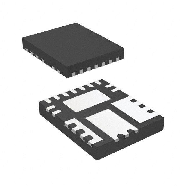
ICGOO电子元器件商城为您提供TPS54335DDA由Texas Instruments设计生产,在icgoo商城现货销售,并且可以通过原厂、代理商等渠道进行代购。 TPS54335DDA价格参考¥14.50-¥18.12。Texas InstrumentsTPS54335DDA封装/规格:PMIC - 稳压器 - DC DC 开关稳压器, 可调式 降压 开关稳压器 IC 正 0.8V 1 输出 3A 8-PowerSOIC(0.154",3.90mm 宽)。您可以下载TPS54335DDA参考资料、Datasheet数据手册功能说明书,资料中有TPS54335DDA 详细功能的应用电路图电压和使用方法及教程。
TPS54335DDA 是由 Texas Instruments(德州仪器)推出的一款 PMIC - DC/DC 开关稳压器,属于高效同步降压转换器。其主要应用场景如下:

1. 便携式电子设备:
   TPS54335DDA 的高效率和小尺寸设计使其非常适合便携式设备,如智能手机、平板电脑、可穿戴设备等。这些设备对电源管理要求严格,需要在有限空间内提供高效的电压转换。

2. 通信设备:
   该芯片适用于各种通信设备,例如路由器、交换机和基站模块。它能够为通信系统中的处理器、FPGA 和其他关键组件提供稳定的电源支持。

3. 工业自动化:
   在工业领域,TPS54335DDA 可用于 PLC(可编程逻辑控制器)、传感器接口和数据采集系统中。其宽输入电压范围(4.5V 至 28V)和高达 3A 的输出电流能力,使其适应多种工业电源环境。

4. 嵌入式计算:
   对于嵌入式系统(如单板计算机或 IoT 网关),TPS54335DDA 提供了紧凑且高效的电源解决方案,确保系统运行稳定并降低功耗。

5. 医疗设备:
   在便携式医疗设备(如血糖仪、脉搏血氧仪)中,这款芯片的低静态电流和高效率特性有助于延长电池寿命,同时保持设备的小型化。

6. 汽车电子:
   虽然 TPS54335DDA 不是专门针对汽车级应用设计,但其性能特点使其可以应用于非关键车载子系统,例如信息娱乐系统或传感器模块。

7. 消费类电子产品:
   包括数字电视、机顶盒和音频设备在内的消费类产品,也可以利用 TPS54335DDA 实现高效电源管理,优化整体系统性能。

总结来说,TPS54335DDA 凭借其高效率、宽输入电压范围和紧凑封装,广泛适用于需要高性能电源管理的各种场景,尤其在对空间和能耗有严格要求的应用中表现出色。
| 参数 | 数值 |
| 产品目录 | 集成电路 (IC)半导体 |
| 描述 | IC REG BUCK ADJ 3A 8SOPWRPAD稳压器—开关式稳压器 4.5-28V Input 3A Sync SD Cnvtr |
| 产品分类 | |
| 品牌 | Texas Instruments |
| 产品手册 | |
| 产品图片 |
|
| rohs | 符合RoHS无铅 / 符合限制有害物质指令(RoHS)规范要求 |
| 产品系列 | 电源管理 IC,稳压器—开关式稳压器,Texas Instruments TPS54335DDASWIFT™ |
| 数据手册 | |
| 产品型号 | TPS54335DDA |
| PCN组件/产地 | |
| PCN设计/规格 | |
| PWM类型 | 电流模式 |
| 产品种类 | 稳压器—开关式稳压器 |
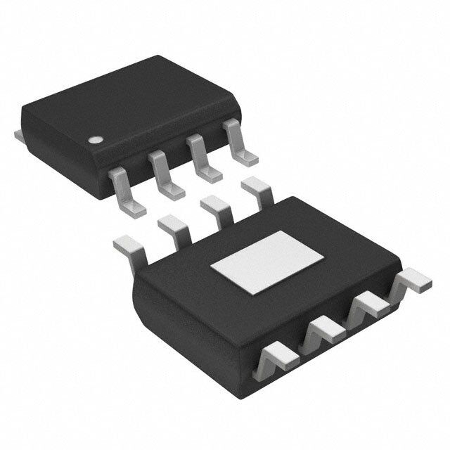
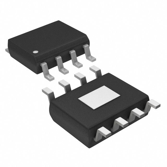
| 供应商器件封装 | 8-SO PowerPad |
| 其它名称 | 296-36208-5 |
| 包装 | 管件 |
| 同步整流器 | 是 |
| 商标 | Texas Instruments |
| 安装类型 | 表面贴装 |
| 安装风格 | SMD/SMT |
| 封装 | Tube |
| 封装/外壳 | 8-SOIC(0.154",3.90mm 宽)裸焊盘 |
| 封装/箱体 | HSOP-8 |
| 工作温度 | -40°C ~ 150°C |
| 工作温度范围 | - 40 C to + 85 C |
| 工厂包装数量 | 75 |
| 开关频率 | 480 kHz |
| 拓扑结构 | Buck |
| 最大工作温度 | + 85 C |
| 最大输入电压 | 28 V |
| 最小工作温度 | - 40 C |
| 最小输入电压 | 4.5 V |
| 标准包装 | 75 |
| 电压-输入 | 4.5 V ~ 28 V |
| 电压-输出 | 0.8 V ~ 25 V |
| 电流-输出 | 3A |
| 电源电压-最小 | 4.5 V |
| 类型 | 降压(降压) |
| 输出数 | 1 |
| 输出电压 | 800 mV to 25 V |
| 输出电流 | 3 A |
| 输出端数量 | 1 Output |
| 输出类型 | 可调式 |
| 频率-开关 | 50kHz ~ 1.5MHz |


- 商务部:美国ITC正式对集成电路等产品启动337调查
- 曝三星4nm工艺存在良率问题 高通将骁龙8 Gen1或转产台积电
- 太阳诱电将投资9.5亿元在常州建新厂生产MLCC 预计2023年完工
- 英特尔发布欧洲新工厂建设计划 深化IDM 2.0 战略
- 台积电先进制程称霸业界 有大客户加持明年业绩稳了
- 达到5530亿美元!SIA预计今年全球半导体销售额将创下新高
- 英特尔拟将自动驾驶子公司Mobileye上市 估值或超500亿美元
- 三星加码芯片和SET,合并消费电子和移动部门,撤换高东真等 CEO
- 三星电子宣布重大人事变动 还合并消费电子和移动部门
- 海关总署:前11个月进口集成电路产品价值2.52万亿元 增长14.8%


PDF Datasheet 数据手册内容提取
Product Sample & Technical Tools & Support & Reference Folder Buy Documents Software Community Design TPS54335,TPS54336 SLVSC03C–MAY2013–REVISEDDECEMBER2014 TPS5433x 4.5- to 28-V Input, 3-A Output, Synchronous SWIFT™ Step-Down DC-DC Converter 1 Features 3 Description • Synchronous128-mΩand84-mΩ MOSFETsfor The TPS5433x family of devices are synchronous 1 converters with an input-voltage range of 4.5 to 28 V. 3-AContinuousOutputCurrent These devices include an integrated low-side • TPS54335:Internal2-msSoft-Start, switching FET that eliminates the need for an 50-kHzto1.5-MHzAdjustableFrequency externaldiodewhichreducescomponentcount. • TPS54336:AdjustableSoft-Start, Efficiency is maximized through the integrated 128- Fixed340-kHzFrequency mΩ and 84-mΩ MOSFETs, low I and pulse skipping Q • Low2-µAShutdown,QuiescentCurrent at light loads. Using the enable pin, the shutdown • 0.8-VVoltageReferencewith ±0.8%Accuracy supply current is reduced to 2 μA. This step-down (buck) converter provides accurate regulation for a • CurrentModeControl variety of loads with a well-regulated voltage • MonotonicStartupintoPre-BiasedOutputs referencethatis1.5%overtemperature. • PulseSkippingforLight-LoadEfficiency Cycle-by-cycle current limiting on the high-side • HiccupModeOvercurrentProtection MOSFET protects the TPS5433x family of devices in • ThermalShutdown(TSD)and overload situations and is enhanced by a low-side OvervoltageTransitionProtection sourcing current limit which prevents current runaway. A low-side sinking current-limit turns off the • 8-PinSOPowerPAD™and10-PinVSON low-side MOSFET to prevent excessive reverse Packages current. Hiccup protection is triggered if the overcurrent condition continues for longer than the 2 Applications preset time. Thermal shutdown disables the device • ConsumerApplicationssuchasaDigitalTV when the die temperature exceeds the threshold and enables the device again after the built-in thermal (DTV),SetTopBox(STB,DVD/Blu-rayPlayer), hiccuptime. LCDDisplay,CPE(CableModem,WiFiRouter), DLPProjectors,SmartMeters DeviceInformation(1) • BatteryChargers PARTNUMBER PACKAGE BODYSIZE(NOM) • IndustrialandCarAudioPowerSupplies SOPowerPAD(8) 4.89mm×3.90mm • 5-V,12-V,and24-VDistributedPowerBusSupply TPS54335 VSON(10) 3.00mm×3.00mm SOPowerPAD(8) 4.89mm×3.90mm TPS54336 VSON(10) 3.00mm×3.00mm (1) For all available packages, see the orderable addendum at theendofthedatasheet. 4 Simplified Schematic VIN VIN VIN VIN C1 C1 TPS54335 TPS54336 CBOOT CBOOT EN BOOT EN BOOT LO LO PH VOUT PH VOUT RT SS COMP CO COMP CO CC RO1 CC RO1 RRT C2 RC GNDVSENSE RO2 CSS C2 RC GNDVSENSE RO2 1 An IMPORTANT NOTICE at the end of this data sheet addresses availability, warranty, changes, use in safety-critical applications, intellectualpropertymattersandotherimportantdisclaimers.PRODUCTIONDATA.
TPS54335,TPS54336 SLVSC03C–MAY2013–REVISEDDECEMBER2014 www.ti.com Table of Contents 1 Features.................................................................. 1 8.3 FeatureDescription.................................................10 2 Applications........................................................... 1 8.4 DeviceFunctionalModes........................................18 3 Description............................................................. 1 9 ApplicationandImplementation........................ 19 4 SimplifiedSchematic............................................. 1 9.1 ApplicationInformation............................................19 9.2 TypicalApplications................................................19 5 RevisionHistory..................................................... 2 10 PowerSupplyRecommendations..................... 31 6 PinConfigurationandFunctions......................... 3 11 Layout................................................................... 32 7 Specifications......................................................... 4 11.1 LayoutGuidelines.................................................32 7.1 AbsoluteMaximumRatings .....................................4 11.2 LayoutExample....................................................32 7.2 ESDRatings..............................................................4 12 DeviceandDocumentationSupport................. 33 7.3 RecommendedOperatingConditions.......................4 7.4 ThermalInformation..................................................5 12.1 DeviceSupport......................................................33 7.5 ElectricalCharacteristics...........................................5 12.2 DocumentationSupport........................................33 7.6 TimingRequirements................................................6 12.3 RelatedLinks........................................................33 7.7 TypicalCharacteristics..............................................6 12.4 Trademarks...........................................................33 12.5 ElectrostaticDischargeCaution............................33 8 DetailedDescription.............................................. 9 12.6 Glossary................................................................33 8.1 Overview...................................................................9 13 Mechanical,Packaging,andOrderable 8.2 FunctionalBlockDiagram.......................................10 Information........................................................... 33 5 Revision History NOTE:Pagenumbersforpreviousrevisionsmaydifferfrompagenumbersinthecurrentversion. ChangesfromRevisionB(September2013)toRevisionC Page • AddedtheESDRatingstableandthefollowingsections:PinConfigurationandFunctions,FeatureDescription, DeviceFunctionalModes,ApplicationandImplementation,PowerSupplyRecommendations,Layout,Deviceand DocumentationSupport,andMechanical,Packaging,andOrderableInformation................................................................ 1 ChangesfromRevisionA(July2013)toRevisionB Page • DeletedPREVIEWwatermarkfromTPS54335DRCpinoutimage....................................................................................... 3 • CorrectedEquation27.......................................................................................................................................................... 23 ChangesfromOriginal(May2013)toRevisionA Page • Changedtitlefrom"....StepDownSWIFT™Converter"to"....SWIFT™Step-DownVoltageRegulator"andchanged productstatusfrom"ProductionData"to"ProductMix"......................................................................................................... 1 • ChangedFeaturebulletfrom"ThermalandOvervoltageTransientProtection"to"ThermalShutdownand OvervoltageTransitionProtection"......................................................................................................................................... 1 • Addedtext"...and10-pinSON"toFeaturebullet................................................................................................................... 1 • ChangedApplicationsbulletfrom"...suchasDTV,SetTopBoxes,LCDdisplays,CPEEquipment"to"....suchasa DigitalTV(DTV),SetTopBox(STB,DVD/Blu-rayPlayer),LCDDisplay,CPE(CableModem,WiFiRouter),DLP Projectors,SmartMeters"....................................................................................................................................................... 1 • ChangedApplicationsbulletfrom"...DistributedPowerSystems"to"...DistributedPowerBusSupply................................ 1 • ChangedSimplifiedSchematicimagesforreadability........................................................................................................... 1 • AddedSON(DRC)pinassignmentdrawingsandpindescriptions....................................................................................... 3 • AddedDRCpackagetoThermalInformationtable................................................................................................................ 5 • ChangedReferencevoltageMINspecfrom"0.792"to"0.7936"andMAXfrom"0.808"to"0.8064"forT =25°C J condition................................................................................................................................................................................. 5 • Deleted"Erroramplifierdcgain"specfromElectricalCharacteristicstable.......................................................................... 5 • AddedTPS54336DRCLoadandLineRegulationcharacteristicsgraphs.......................................................................... 29 2 SubmitDocumentationFeedback Copyright©2013–2014,TexasInstrumentsIncorporated ProductFolderLinks:TPS54335 TPS54336
TPS54335,TPS54336 www.ti.com SLVSC03C–MAY2013–REVISEDDECEMBER2014 6 Pin Configuration and Functions DDAPackage DDAPackage 8-PinSOPowerPAD 8-PinSOPowerPAD TPS54335TopView TPS54336TopView BOOT 1 8 RT BOOT 1 8 SS VIN 2 7 EN VIN 2 7 EN PowerPAD PowerPAD PH 3 (9) 6 COMP PH 3 (9) 6 COMP GND 4 5 VSENSE GND 4 5 VSENSE DRCPackage DRCPackage 10-PinVSONWithExposedThermalPad 10-PinVSONWithExposedThermalPad TPS54335TopView TPS54336TopView VIN 1 10 RT VIN 1 10 SS PH 2 9 BOOT PH 2 9 BOOT Exposed Exposed Thermal Thermal GND 3 8 EN GND 3 8 EN Pad Pad GND 4 (11) 7 COMP GND 4 (11) 7 COMP GND 5 6 VSENSE GND 5 6 VSENSE PinFunctions PIN SO I/O DESCRIPTION NAME Power VSON PAD AbootstrapcapacitorisrequiredbetweentheBOOTandPHpins.Ifthevoltageonthis BOOT 1 9 O capacitorisbelowtheminimumrequiredbytheoutputdevice,theoutputisforcedto switchoffuntilthecapacitorisrefreshed. Thispinistheerror-amplifieroutputandtheinputtotheoutputswitch-currentcomparator. COMP 6 7 O Connectfrequencycompensationcomponentstothispin. EN 7 8 I Thispinistheenablepin.FloattheENpintoenable. 3 GND 4 4 — Ground 5 PH 3 2 O ThePHpinisthesourceoftheinternalhigh-sidepowerMOSFET. ConnecttheRTpintoanexternaltimingresistortoadjusttheswitchingfrequencyofthe RT(TPS54335) device. 8 10 O TheSSpinisthesoft-startandtrackingpin.Anexternalcapacitorconnectedtothispin SS(TPS54336) setstheinternalvoltage-referencerisetime.Thevoltageonthispinoverridestheinternal reference. VIN 2 1 — Thispinisthe4.5-to28-Vinputsupplyvoltage. VSENSE 5 6 I Thispinistheinvertingnodeofthetransconductance(gm)erroramplifier. PowerPAD(SO only) 9 — Forproperoperation,connecttheGNDpintotheexposedthermalpad.Thisthermalpad — shouldbeconnectedtoanyinternalPCBgroundplaneusingmultipleviasforgood Thermalpad — 11 thermalperformance. (VSONonly) Copyright©2013–2014,TexasInstrumentsIncorporated SubmitDocumentationFeedback 3 ProductFolderLinks:TPS54335 TPS54336
TPS54335,TPS54336 SLVSC03C–MAY2013–REVISEDDECEMBER2014 www.ti.com 7 Specifications 7.1 Absolute Maximum Ratings(1) MIN MAX UNIT VIN –0.3 30 EN –0.3 6 BOOT –0.3 (PH+7.5) Inputvoltage VSENSE –0.3 3 V COMP –0.3 3 RT –0.3 3 SS –0.3 3 BOOT-PH 0 7.5 Outputvoltage PH –1 30 V PH,10-nstransient –3.5 30 V (GNDtoexposedthermalpad) –0.2 0.2 V DIFF EN 100 100 µA Sourcecurrent RT 100 100 PH Current-limit A PH Current-limit A Sinkcurrent COMP 200 200 µA Operatingjunctiontemperature –40 150 °C Storagetemperature,T –65 150 °C stg (1) Stressesbeyondthoselistedundertheabsolutemaximumratingsmaycausepermanentdamagetothedevice.Thesearestress ratingsonly,andfunctionaloperationofthedeviceattheseoranyotherconditionsbeyondthoseindicatedundertherecommended operatingconditionsisnotimplied.Exposuretoabsolute-maximum-ratedconditionsforextendedperiodsmayaffectdevicereliability. 7.2 ESD Ratings VALUE UNIT Humanbodymodel(HBM),perANSI/ESDA/JEDECJS–001,allpins(1) 2000 V(ESD) Electrostaticdischarge Chargeddevicemodel(CDM),perJEDECspecificationJESD22-C101, V allpins(2) 500 (1) JEDECdocumentJEP155statesthat500-VHBMallowssafemanufacturingwithastandardESDcontrolprocess. (2) JEDECdocumentJEP157statesthat250-VCDMallowssafemanufacturingwithastandardESDcontrolprocess. 7.3 Recommended Operating Conditions overoperatingfree-airtemperaturerange(unlessotherwisenoted) MIN MAX UNIT V Supplyinputvoltage 4.5 28 V SS V Outputvoltage 0.8 24 V OUT I Outputcurrent 0 3 A OUT T Operatingjunctiontemperature –40 150 °C J 4 SubmitDocumentationFeedback Copyright©2013–2014,TexasInstrumentsIncorporated ProductFolderLinks:TPS54335 TPS54336
TPS54335,TPS54336 www.ti.com SLVSC03C–MAY2013–REVISEDDECEMBER2014 7.4 Thermal Information DDA DRC THERMALMETRIC(1) UNIT 8PINS 10PINS R Junction-to-ambientthermalresistance 42.1 43.9 θJA R Junction-to-case(top)thermalresistance 50.9 55.4 θJC(top) R Junction-to-boardthermalresistance 31.8 18.9 θJB °C/W ψ Junction-to-topcharacterizationparameter 8 0.7 JT ψ Junction-to-boardcharacterizationparameter 13.5 19.1 JB R Junction-to-case(bottom)thermalresistance 7.1 5.3 θJC(bot) (1) Formoreinformationabouttraditionalandnewthermalmetrics,seetheICPackageThermalMetricsapplicationreport,SPRA953. 7.5 Electrical Characteristics Theelectricalratingsspecifiedinthissectionapplytoallspecificationsinthisdocumentunlessotherwisenoted.These specificationsareinterpretedasconditionsthatwillnotdegradetheparametricorfunctionalspecificationsofthedevicefor thelifeoftheproductcontainingit.T =–40°Cto150°C,VIN=4.5to28V,(unlessotherwisenoted) J PARAMETER TESTCONDITIONS MIN TYP MAX UNIT SUPPLYVOLTAGEANDUVLO(VINPIN) Operatinginputvoltage 4.5 28 V InputUVLOthreshold RisingVIN 4 4.5 V InputUVLOhysteresis 180 400 mV VIN-shutdownsupplycurrent EN=0V 2 10 µA VIN-operatingnon-switchingsupply VSENSE=810mV 310 800 µA current ENABLE(ENPIN) Enablethreshold Rising 1.21 1.28 V Enablethreshold Falling 1.1 1.17 V Inputcurrent EN=1.1V 1.15 µA Hysteresiscurrent EN=1.3V 3.3 µA VOLTAGEREFERENCE T =25°C 0.7936 0.8 0.8064 J Reference V 0.788 0.8 0.812 MOSFET BOOT-PH=3V 160 280 mΩ High-sideswitchresistance(1) BOOT-PH=6V 128 230 mΩ Low-sideswitchresistance(1) VIN=12V 84 170 mΩ ERRORAMPLIFIER Error-amplifiertransconductance(gm) –2µA<I <2µA,V =1V 1300 µmhos COMP COMP Error-amplifiersourceandsink V =1V,100-mVoverdrive 100 µA COMP Startswitchingpeakcurrentthreshold 0.5 A COMPtoI gm 8 A/V SWITCH CURRENT-LIMIT High-sideswitchcurrent-limitthreshold 4 4.9 6.5 A Low-sideswitchsourcingcurrent-limit 3.5 4.7 6.1 A Low-sideswitchsinkingcurrent-limit 0 A Hiccupwaittime 512 Cycles Hiccuptimebeforerestart 16384 Cycles (1) Measuredatpins Copyright©2013–2014,TexasInstrumentsIncorporated SubmitDocumentationFeedback 5 ProductFolderLinks:TPS54335 TPS54336
TPS54335,TPS54336 SLVSC03C–MAY2013–REVISEDDECEMBER2014 www.ti.com Electrical Characteristics (continued) Theelectricalratingsspecifiedinthissectionapplytoallspecificationsinthisdocumentunlessotherwisenoted.These specificationsareinterpretedasconditionsthatwillnotdegradetheparametricorfunctionalspecificationsofthedevicefor thelifeoftheproductcontainingit.T =–40°Cto150°C,VIN=4.5to28V,(unlessotherwisenoted) J PARAMETER TESTCONDITIONS MIN TYP MAX UNIT THERMALSHUTDOWN Thermalshutdown 160 175 °C Thermalshutdownhysteresis 10 °C Thermalshutdownhiccuptime 32768 Cycles PHPIN Minimumontime Measuredat90%to90%ofVIN,I =2A 94 145 ns PH Minimumofftime BOOT-PH≥3V 0% BOOTPIN BOOT-PHUVLO 2.1 3 V SOFTSTART Internalsoft-starttime TPS54335 2 ms soft-startchargecurrent TPS54336 2.3 µA 7.6 Timing Requirements MIN TYP MAX UNIT SWITCHINGFREQUENCY TPS54335 50 1500 kHz TPS54335,R =100kΩ 384 480 576 kHz RT Switchingfrequencyrange TPS54335,R =1000kΩ,–40°Cto105°C 40 50 60 kHz RT TPS54335,R =30kΩ 1200 1500 1800 kHz RT Internalswitchingfrequency TPS54336 272 340 408 kHz 7.7 Typical Characteristics 210 140 130 190 120 (cid:13) (cid:12) 170 (cid:13) (cid:12) m m 110 On Resistance ( 111135000 On Resistance ( 1089000 70 90 60 70 50 ±50 ±25 0 25 50 75 100 125 150 ±50 ±25 0 25 50 75 100 125 150 Junction Temperature (ƒC) C001 Junction Temperature (ƒC) C002 VIN=12V VIN=12V Figure1.High-SideMOSFETonResistancevsJunction Figure2.Low-SideMOSFETonResistancevsJunction Temperature Temperature 6 SubmitDocumentationFeedback Copyright©2013–2014,TexasInstrumentsIncorporated ProductFolderLinks:TPS54335 TPS54336
TPS54335,TPS54336 www.ti.com SLVSC03C–MAY2013–REVISEDDECEMBER2014 Typical Characteristics (continued) 0.808 495 e (V) 0.804 y (kHz) 448950 c c n n e e efer 0.800 equ 480 Voltage R 0.796 scillator Fr 475 O 470 0.792 465 ±50 ±25 0 25 50 75 100 125 150 ±50 ±25 0 25 50 75 100 125 150 Junction Temperature (ƒC) C003 Junction Temperature (ƒC) C004 Figure3.VoltageReferencevsJunctionTemperature Figure4.OscillatorFrequencyvsJunctionTemperature 1.230 3.50 3.45 V) 1.225 A) UVLO Threshold ( 1.220 (cid:29)eresis Current ( 333...334050 N- 1.215 yst E H 3.25 1.210 3.20 ±50 ±25 0 25 50 75 100 125 150 ±50 ±25 0 25 50 75 100 125 150 Junction Temperature (ƒC) C005 Junction Temperature (ƒC) C006 V =12V V =12V IN IN Figure5.UVLOThresholdvsJunctionTemperature Figure6.HysteresisCurrentvsJunctionTemperature 1.2 400 (cid:29)Pullup Current (A) 11..111.271555 Non-Switching Operating (cid:29) Quiescent Current (A) 233505000 TTJJ == ±±4400ƒƒCC TTJJ == 2255ƒƒCC 1.1 200 TTJJ == 115500ƒƒCC ±50 ±25 0 25 50 75 100 125 150 4 8 12 16 20 24 28 Junction Temperature (ƒC) C007 Input Voltage (V) C008 V =12V IN Figure7.PullupCurrentvsJunctionTemperature Figure8.Non-SwitchingOperatingQuiescentCurrentvs InputVoltage Copyright©2013–2014,TexasInstrumentsIncorporated SubmitDocumentationFeedback 7 ProductFolderLinks:TPS54335 TPS54336
TPS54335,TPS54336 SLVSC03C–MAY2013–REVISEDDECEMBER2014 www.ti.com Typical Characteristics (continued) 10 2.40 TTJ = = ± ±4400ƒƒCC (cid:29)A) TTJJJ = = 2 255ƒƒCC nt ( 8 TTJJ = = 1 15500ƒƒCC A) 2.35 e (cid:29) Quiescent Curr 46 harge Current ( 2.30 n C ow S 2.25 d 2 S ut h S 0 2.20 4 8 12 16 20 24 28 ±50 ±25 0 25 50 75 100 125 150 Input Voltage (V) C009 Junction Temperature (ƒC) C010 EN=0V Figure9.ShutdownQuiescentCurrentvsInputVoltage Figure10.SSChargeCurrentvsJunctionTemperature 120 6.0 s) %) me (n 110 atio ( Minimum Controllable On Ti 1089000 Minimum Controllable Duty R 45..00 70 3.0 ±50 ±25 0 25 50 75 100 125 150 ±50 ±25 0 25 50 75 100 125 150 Junction Temperature (ƒ) C011 Junction Temperature (ƒC) C012 V =12V V =12V IN IN Figure11.MinimumControllableOnTimevsJunction Figure12.MinimumControllableDutyRatiovsJunction Temperature Temperature 2.3 6.0 TT=J –=4 -04°0Cƒ J (cid:29)O Threshhold (A) 2.2 mitThreshold(A) 55..05 TTJJTT==JJ 21==55 210°55C°ƒC0ƒ T-PH UVL 2.1 Current-Li 4.5 O O B 2.0 4.0 ±50 ±25 0 25 50 75 100 125 150 4 8 12 16 20 24 28 Junction Temperature (ƒC) C013 InputVoltage(V) C014 Figure13.BOOT-PHUVLOThresholdvsJunction Figure14.Current-LimitThresholdvsInputVoltage Temperature 8 SubmitDocumentationFeedback Copyright©2013–2014,TexasInstrumentsIncorporated ProductFolderLinks:TPS54335 TPS54336
TPS54335,TPS54336 www.ti.com SLVSC03C–MAY2013–REVISEDDECEMBER2014 8 Detailed Description 8.1 Overview The device is a 28-V, 3-A, synchronous step-down (buck) converter with two integrated n-channel MOSFETs. To improve performance during line and load transients the device implements a constant-frequency, peak current- modecontrolwhichreducesoutputcapacitanceandsimplifiesexternalfrequency-compensationdesign. The device has been designed for safe monotonic startup into pre-biased loads. The device has a typical default startupvoltageof4V.TheENpinhasaninternalpullup-currentsourcethatcanprovideadefaultconditionwhen the EN pin is floating for the device to operate. The total operating current for the device is 310 µA (typical) when notswitchingandundernoload.Whenthedeviceisdisabled,thesupplycurrentislessthan5 μA. The integrated 128-mΩ and 84-mΩ MOSFETs allow for high-efficiency power-supply designs with continuous outputcurrentsupto3A. The device reduces the external component count by integrating the boot recharge diode. The bias voltage for the integrated high-side MOSFET is supplied by a capacitor between the BOOT and PH pins. The boot capacitor voltage is monitored by an UVLO circuit and turns off the high-side MOSFET when the voltage falls below a presetthreshold.Theoutputvoltagecanbesteppeddowntoaslowasthe0.8-Vreferencevoltage. The device minimizes excessive output overvoltage transients by taking advantage of the overvoltage power- good comparator. When the regulated output voltage is greater than 106% of the nominal voltage, the overvoltage comparator is activated, and the high-side MOSFET is turned off and masked from turning on until theoutputvoltageislowerthan104%. TheTPS54335devicehasawideswitchingfrequencyof50kHzto1500kHzwhichallowsforefficiencyandsize optimization when selecting the output filter components. The internal 2-ms soft-start time is implemented to minimizeinrushcurrents. The TPS54336 device has a fixed 340-kHz switching frequency. The device adjusts the soft-start time with the SSpin. Copyright©2013–2014,TexasInstrumentsIncorporated SubmitDocumentationFeedback 9 ProductFolderLinks:TPS54335 TPS54336
TPS54335,TPS54336 SLVSC03C–MAY2013–REVISEDDECEMBER2014 www.ti.com 8.2 Functional Block Diagram EN VIN Thermal UVLO Hiccup Enable Ip Ih Comparator Shutdown Logic Hiccup Shutdown Enable Threshold OV Boot Charge Minimum Clamp Current Pulse Skip Sense ERROR AMPLIFIER VSENSE Boot BOOT + UVLO SS + (TPS54336) RVefoeltraegnece HCSoC mMupOrraeSrnaFttE oTr Powearn Sd tage PH Deadtime Control Logic Slope Compensation VIN Regulator Hiccup Shutdown Overload Maximum Oscillator LS MOSFET Recovery Clamp Current-Limit Current Sense GND COMP RT EXPOSED THERMAL PAD (TPS54335) 8.3 Feature Description 8.3.1 Fixed-FrequencyPWMControl The device uses a fixed-frequency, peak current-mode control. The output voltage is compared through external resistors on the VSENSE pin to an internal voltage reference by an error amplifier which drives the COMP pin. An internal oscillator initiates the turn on of the high-side power switch. The error amplifier output is compared to the current of the high-side power switch. When the power-switch current reaches the COMP voltage level the high-sidepowerswitchisturnedoffandthelow-sidepowerswitchisturnedon.TheCOMPpinvoltageincreases and decreases as the output current increases and decreases. The device implements a current-limit by clamping the COMP pin voltage to a maximum level and also implements a minimum clamp for improved transient-responseperformance. 8.3.2 Light-LoadOperation The device monitors the peak switch current of the high-side MOSFET. When the peak switch current is lower than 0.5 A (typical), the device stops switching to boost the efficiency until the peak switch current again rises higherthan0.5A(typical). 10 SubmitDocumentationFeedback Copyright©2013–2014,TexasInstrumentsIncorporated ProductFolderLinks:TPS54335 TPS54336
TPS54335,TPS54336 www.ti.com SLVSC03C–MAY2013–REVISEDDECEMBER2014 Feature Description (continued) 8.3.3 VoltageReference The voltage-reference system produces a precise ±1.5% voltage-reference over temperature by scaling the outputofatemperature-stablebandgapcircuit. 8.3.4 AdjustingtheOutputVoltage The output voltage is set with a resistor divider from the output node to the VSENSE pin. Using divider resistors with 1% tolerance or better is recommended. Begin with a value of 10 kΩ for the upper resistor divider, R1, and use Equation 1 to calculate the value of R2. Consider using larger value resistors to improve efficiency at light loads. If the values are too high then the regulator is more susceptible to noise and voltage errors from the VSENSEinputcurrentarenoticeable. V R2= REF ´R1 V -V OUT REF (1) 8.3.5 EnablingandAdjustingUndervoltageLockout The EN pin provides electrical on and off control of the device. When the EN pin voltage exceeds the threshold voltage, the device begins operation. If the EN pin voltage is pulled below the threshold voltage, the regulator stopsswitchingandentersthelow-quiescent(I )state. Q TheENpinhasaninternalpullup-currentsourcewhichallowstheusertofloattheENpintoenablethedevice.If an application requires control of the EN pin, use open-drain or open-collector output logic to interface with the pin. The device implements internal undervoltage-lockout (UVLO) circuitry on the VIN pin. The device is disabled when the VIN pin voltage falls below the internal VIN UVLO threshold. The internal VIN UVLO threshold has a hysteresisof180mV. If an application requires a higher UVLO threshold on the VIN pin, then the EN pin can be configured as shown in Figure 15. When using the external UVLO function, setting the hysteresis at a value greater than 500 mV is recommended. The EN pin has a small pullup-current, I , which sets the default state of the pin to enable when no external p components are connected. The pullup current is also used to control the voltage hysteresis for the UVLO function because it increases by I when the EN pin crosses the enable threshold. Use Equation 2, and h Equation3tocalculatethevaluesofR1andR2foraspecifiedUVLOthreshold. Device VIN I I p h R1 R2 EN Figure15. AdjustableVINUndervoltageLockout Copyright©2013–2014,TexasInstrumentsIncorporated SubmitDocumentationFeedback 11 ProductFolderLinks:TPS54335 TPS54336
TPS54335,TPS54336 SLVSC03C–MAY2013–REVISEDDECEMBER2014 www.ti.com Feature Description (continued) æV ö V ç ENfalling ÷ - V START ç ÷ STOP V è ENrising ø R1= æ V ö I ç1- ENfalling ÷+I pç ÷ h V è ENrising ø where • I =1.15μA P • I =3.3μA H • V =1.17V ENfalling • V =1.21V (2) ENrising R1´V ENfalling R2= V -V +R1(I +I ) STOP ENfalling p h where • I =1.15μA P • I =3.3μA H • V =1.17V ENfalling • V =1.21V (3) ENrising 8.3.6 ErrorAmplifier The device has a transconductance amplifier as the error amplifier. The error amplifier compares the VSENSE voltage to the lower of the internal soft-start voltage or the internal 0.8-V voltage reference. The transconductance of the error amplifier is 1300 μA/V (typical). The frequency compensation components are placedbetweentheCOMPpinandground. 8.3.7 SlopeCompensationandOutputCurrent The device adds a compensating ramp to the signal of the switch current. This slope compensation prevents subharmonic oscillations as the duty cycle increases. The available peak inductor current remains constant over thefullduty-cyclerange. 8.3.8 SafeStartupintoPre-BiasedOutputs The device has been designed to prevent the low-side MOSFET from discharging a pre-biased output. During monotonic pre-biased startup, both high-side and low-side MOSFETs are not allowed to be turned on until the internalsoft-startvoltage(TPS54335),orSSpinvoltage(TPS54336)ishigherthanVSENSEpinvoltage. 8.3.9 BootstrapVoltage(BOOT) The device has an integrated boot regulator. The boot regulator requires a small ceramic capacitor between the BOOT and PH pins to provide the gate-drive voltage for the high-side MOSFET. The boot capacitor is charged when the BOOT pin voltage is less than the VIN voltage and when the BOOT-PH voltage is below regulation. The value of this ceramic capacitor should be 0.1 μF. A ceramic capacitor with an X7R or X5R grade dielectric with a voltage rating of 10 V or higher is recommended because of the stable characteristics over temperature and voltage. When the voltage between BOOT and PH pins drops below the BOOT-PH UVLO threshold, which is 2.1 V (typical), the high-side MOSFET turns off and the low-side MOSFET turns on, allowing the boot capacitortorecharge. 12 SubmitDocumentationFeedback Copyright©2013–2014,TexasInstrumentsIncorporated ProductFolderLinks:TPS54335 TPS54336
TPS54335,TPS54336 www.ti.com SLVSC03C–MAY2013–REVISEDDECEMBER2014 Feature Description (continued) 8.3.10 AdjustableSwitchingFrequency(TPS54335Only) To determine the RT resistance, R , for a given switching frequency, use Equation 4 or the curve in Figure 16. RT To reduce the solution size, set the switching frequency as high as possible, but consider the tradeoffs of the supplyefficiencyandminimumcontrollableontime. R (kW)=55300´ƒ -1.025(kHz) RT SW (4) 1000 (cid:13)) 800 k e ( nc 600 a st si e R 400 et S T R 200 0 0 250 500 750 1000 1250 1500 Oscillator Frequency (kHz) C026 Figure16. RTSetResistorvsSwitchingFrequency 8.3.11 Soft-Start(TPS54336Only) The TPS54336 device uses the lower voltage of the internal voltage reference or the SS pin voltage as the reference voltage and regulates the output accordingly. A capacitor on the SS pin to ground implements a soft- start time. The device has an internal pullup current source of 2.3 μA that charges the external soft-start capacitor.UseEquation5tocalculatethesofttime(t ,10%to90%)andsoftcapacitor(C ). SS SS C (nF) ´ V (V) t (ms)= SS REF SS I (µA) SS where • V isthevoltagereference(0.8V) REF • I isthesoft-startchargecurrent(2.3μA) (5) SS When the input UVLO is triggered, the device stops switching and enters low-current operation when either the EN pin is pulled below 1.21 V or a thermal-shutdown event occurs. At the subsequent power-up, when the shutdown condition is removed, the device does not begin switching until it has discharged the SS pin to ground ensuringpropersoft-startbehavior. 8.3.12 OutputOvervoltageProtection(OVP) The device incorporates an output overvoltage-protection (OVP) circuit to minimize output voltage overshoot. For example, when the power-supply output is overloaded, the error amplifier compares the actual output voltage to the internal reference voltage. If the VSENSE pin voltage is lower than the internal reference voltage for a considerable time, the output of the error amplifier demands maximum output current. When the condition is removed, the regulator output rises and the error-amplifier output transitions to the steady-state voltage. In some applications with small output capacitance, the power-supply output voltage can respond faster than the error amplifier which leads to the possibility of an output overshoot. The OVP feature minimizes the overshoot by comparing the VSENSE pin voltage to the OVP threshold. If the VSENSE pin voltage is greater than the OVP threshold, the high-side MOSFET is turned off which prevents current from flowing to the output and minimizes output overshoot. When the VSENSE voltage drops lower than the OVP threshold, the high-side MOSFET is allowedtoturnonatthenextclockcycle. Copyright©2013–2014,TexasInstrumentsIncorporated SubmitDocumentationFeedback 13 ProductFolderLinks:TPS54335 TPS54336
TPS54335,TPS54336 SLVSC03C–MAY2013–REVISEDDECEMBER2014 www.ti.com Feature Description (continued) 8.3.13 OvercurrentProtection The device is protected from overcurrent conditions by cycle-by-cycle current limiting on both the high-side MOSFETandthelow-sideMOSFET. 8.3.13.1 High-SideMOSFETOvercurrentProtection The device implements current mode control which uses the COMP pin voltage to control the turn off of the high- side MOSFET and the turn on of the low-side MOSFET on a cycle-by-cycle basis. During each cycle, the switch current and the current reference generated by the COMP pin voltage are compared. When the peak switch currentintersectsthecurrentreferencethehigh-sideswitchturnsoff. 8.3.13.2 Low-SideMOSFETOvercurrentProtection While the low-side MOSFET is turned on, the conduction current is monitored by the internal circuitry. During normal operation the low-side MOSFET sources current to the load. At the end of every clock cycle, the low-side MOSFET sourcing current is compared to the internally set low-side sourcing current-limit. If the low-side sourcing current-limit is exceeded, the high-side MOSFET does not turn on and the low-side MOSFET stays on for the next cycle. The high-side MOSFET turns on again when the low-side current is below the low-side sourcingcurrent-limitatthestartofacycle. The low-side MOSFET can also sink current from the load. If the low-side sinking current-limit is exceeded the low-side MOSFET turns off immediately for the remainder of that clock cycle. In this scenario, both MOSFETs areoffuntilthestartofthenextcycle. Furthermore, if an output overload condition (as measured by the COMP pin voltage) occurs for more than the hiccup wait time, which is programmed for 512 switching cycles, the device shuts down and restarts after the hiccup time of 16384 cycles. The hiccup mode helps to reduce the device power dissipation under severe overcurrentconditions. 8.3.14 ThermalShutdown The internal thermal-shutdown circuitry forces the device to stop switching if the junction temperature exceeds 175°C typically. When the junction temperature drops below 165°C typically, the internal thermal-hiccup timer begins to count. The device reinitiates the power-up sequence after the built-in thermal-shutdown hiccup time (32768cycles)isover. 8.3.15 Small-SignalModelforLoopResponse Figure 17 shows an equivalent model for the device control loop which can be modeled in a circuit-simulation program to check frequency and transient responses. The error amplifier is a transconductance amplifier with a gm of 1300 μA/V. The error amplifier can be modeled using an ideal voltage-controlled current source. The resistor, R (3.07 MΩ), and capacitor, C (20.7 pF), model the open-loop gain and frequency response of the oea oea error amplifier. The 1-mV AC-voltage source between the nodes a and b effectively breaks the control loop for the frequency response measurements. Plotting ac-c and c-b show the small-signal responses of the power stageandfrequencycompensationrespectively.Plotting a-bshowsthesmall-signalresponseoftheoverallloop. The dynamic loop response can be checked by replacing the load resistance, R , with a current source with the L appropriateload-stepamplitudeandsteprateinatime-domainanalysis. 14 SubmitDocumentationFeedback Copyright©2013–2014,TexasInstrumentsIncorporated ProductFolderLinks:TPS54335 TPS54336
TPS54335,TPS54336 www.ti.com SLVSC03C–MAY2013–REVISEDDECEMBER2014 Feature Description (continued) PH Power Stage VOUT 8 A/V a b R ESR R1 COMP c R VSENSE L + VREF R3 C O R C2 Coea oea gmea R2 1300 µA/V C1 Figure17. Small-SignalModelForLoopResponse 8.3.16 SimpleSmall-SignalModelforPeakCurrent-ModeControl Figure 18 is a simple small-signal model that can be used to understand how to design the frequency compensation. The device power stage can be approximated to a voltage-controlled current-source (duty-cycle modulator) supplying current to the output capacitor and load resistor. The control-to-output transfer function is shown in Equation 6 and consists of a DC gain, one dominant pole and one ESR zero. The quotient of the change in switch current and the change in the COMP pin voltage (node c in Figure 17) is the power-stage transconductance (gm ) which is 8 A/V for the device. The DC gain of the power stage is the product of gm ps ps and the load resistance, R , with resistive loads as shown in Equation 7. As the load current increases, the DC L gain decreases. This variation with load may seem problematic at first glance, but fortunately the dominant pole moveswiththeloadcurrent(seeEquation8).ThecombinedeffectishighlightedbythedashedlineinFigure19. As the load current decreases, the gain increases and the pole frequency lowers, keeping the 0-dB crossover frequencythesameforthevaryingloadconditionswhichmakesdesigningthefrequencycompensationeasier. V OUT VC R ESR R L gm ps C O Figure18. SimplifiedSmall-SignalModelforPeakCurrent-ModeControl Copyright©2013–2014,TexasInstrumentsIncorporated SubmitDocumentationFeedback 15 ProductFolderLinks:TPS54335 TPS54336
TPS54335,TPS54336 SLVSC03C–MAY2013–REVISEDDECEMBER2014 www.ti.com Feature Description (continued) V OUT VC Adc R ƒ ESR p R L gm ps C O ƒ z Figure19. SimplifiedFrequencyResponseforPeakCurrent-ModeControl æ s ö ç1+ ÷ V è 2p´ƒ ø OUT = Adc´ z VC æ s ö ç1+ ÷ ç 2p´ƒ ÷ è p ø (6) Adc = gm ´ R ps L where • gm isthepowerstagegain(8A/V) ps • R istheloadresistance (7) L 1 ƒ = p C ´ R ´ 2p O L where • C istheoutputcapacitance (8) O 1 ƒ = z C ´ R ´ 2p O ESR where • R istheequivalentseriesresistanceoftheoutputcapacitor (9) ESR 8.3.17 Small-SignalModelforFrequencyCompensation The device uses a transconductance amplifier for the error amplifier and readily supports two of the commonly used Type II compensation circuits and a Type III frequency compensation circuit, as shown in Figure 20. In Type 2A, one additional high frequency pole, C6, is added to attenuate high frequency noise. In Type III, one additional capacitor, C11, is added to provide a phase boost at the crossover frequency. See Designing Type III Compensation for Current Mode Step-Down Converters (SLVA352) for a complete explanation of Type III compensation. The following design guidelines are provided for advanced users who prefer to compensate using the general method. The following equations only apply to designs whose ESR zero is above the bandwidth of the control loopwhichisusuallytruewithceramicoutputcapacitors. 16 SubmitDocumentationFeedback Copyright©2013–2014,TexasInstrumentsIncorporated ProductFolderLinks:TPS54335 TPS54336
TPS54335,TPS54336 www.ti.com SLVSC03C–MAY2013–REVISEDDECEMBER2014 Feature Description (continued) V OUT C11 R8 VSENSE Type 2A Type 2B COMP Type III R9 V + REF gm R4 R4 ea C6 Roea Coea C4 C4 Figure20. TypesofFrequencyCompensation Thegeneraldesignguidelinesfordeviceloopcompensationareasfollows: 1. Determinethecrossoverfrequency,ƒ .Agoodstartingvalueforƒ is1/10thoftheswitchingfrequency,ƒ . c c SW 2. UseEquation10tocalculatethevalueofR4. 2p ´ ƒ ´ V ´ C R4= c OUT O gm ´ V ´ gm ea REF ps where • gm istheGMamplifiergain(1300μA/V) ea • gm isthepowerstagegain(8A/V) ps • V isthereferencevoltage(0.8V) (10) REF 3. PlaceacompensationzeroatthedominantpoleanduseEquation11tocalculatethevalueof ƒ . p æ 1 ö çƒ = ÷ è p CO ´ RL ´ 2pø (11) 4. UseEquation12tocalculatethevalueofC4. R ´ C C4= L O R4 (12) 5. The use of C6 is optional. C6 can be used to cancel the zero from the ESR (equivalent series resistance) of theoutputcapacitorC .Ifused,useEquation13tocalculatethevalueofC6. O R ´ C C6= ESR O R4 (13) 6. Type III compensation can be implemented with the addition of one capacitor, C11. The use of C11 allows for slightly higher loop bandwidths and higher phase margins. If used, use Equation 14 to calculate the value ofC11. 1 C11= (2´p´R8´ƒ ) C (14) Copyright©2013–2014,TexasInstrumentsIncorporated SubmitDocumentationFeedback 17 ProductFolderLinks:TPS54335 TPS54336
TPS54335,TPS54336 SLVSC03C–MAY2013–REVISEDDECEMBER2014 www.ti.com 8.4 Device Functional Modes 8.4.1 OperationWithV <4.5V(minimumV) I I The device is designed to operate with input voltages above 4.5 V. The typical VIN UVLO threshold is 4V and if VIN falls below this threshold the device stops switching. If the EN pin voltage is above EN threshold the device becomesactivewhentheVINpinpassestheUVLOthreshold.. 8.4.2 OperationWithENControl The enable threshold is 1.2-V typical. If the EN pin voltage is below this threshold the device does not switch even though the Vin is above the UVLO threshold. The IC quiescent current is reduced in this state. Once the EN is above the threshold with VIN above UVLO threshold the device is active again and the soft-start sequence isinitiated. 18 SubmitDocumentationFeedback Copyright©2013–2014,TexasInstrumentsIncorporated ProductFolderLinks:TPS54335 TPS54336
TPS54335,TPS54336 www.ti.com SLVSC03C–MAY2013–REVISEDDECEMBER2014 9 Application and Implementation NOTE Information in the following applications sections is not part of the TI component specification, and TI does not warrant its accuracy or completeness. TI’s customers are responsible for determining suitability of components for their purposes. Customers should validateandtesttheirdesignimplementationtoconfirmsystemfunctionality. 9.1 Application Information The TPS5433x are integrated synchronous step-down DC-DC converters which operate with a Vin of 4.5 V to 28V.WEBENCHsoftwareisavailabletoaidinthedesignandanalysisofanapplicationcircuit. 9.2 Typical Applications 9.2.1 TPS54335Application U1 L1 15 µH VIN VIN= 8 to 28 V 2 VTINPS54335BDODOAT 1 C3 0.1 µF VOUT= 5 V, 3Amax VOUT 5 3 C1 C2 VSENSE VSENSE PH C6 C7 R4 10 µF 0.1 µF 7 6 47 µF 47 µF 51.1Ω R1 EN COMP 220 kΩ 8 4 RT GND PAD R3 R5 3.74 kΩ 100 kΩ C5 V 120 pF SENSE R2 R7 C4 R6 43.2 kΩ 143 kΩ 0.012 µF 19.1 kΩ Figure21. TypicalApplicationSchematic,TPS54335 9.2.1.1 DesignRequirements Forthisdesignexample,usetheparameterslistedinTable1. Table1.DesignParameters DESIGNPARAMETER EXAMPLEVALUE Inputvoltagerange 8to28V Outputvoltage 5V Transientresponse,1.5-Aloadstep ΔV =±5% OUT Inputripplevoltage 400mV Outputripplevoltage 30mV Outputcurrentrating 3A OperatingFrequency 340kHz Copyright©2013–2014,TexasInstrumentsIncorporated SubmitDocumentationFeedback 19 ProductFolderLinks:TPS54335 TPS54336
TPS54335,TPS54336 SLVSC03C–MAY2013–REVISEDDECEMBER2014 www.ti.com 9.2.1.2 DetailedDesignProcedure The following design procedure can be used to select component values for the TPS54335 and TPS54336 devices. Alternately, the WEBENCH® software may be used to generate a complete design. The WEBENCH software uses an iterative design procedure and accesses a comprehensive database of components when generating a design. This section presents a simplified discussion of the design process using the TPS54335 device. Forthisdesignexample,usetheinputparameterslistedinTable1. 9.2.1.2.1 SwitchingFrequency The switching frequency of the TPS54335 device is set at 340 kHz to match the internally set frequency of the TPS54336 device for this design. Use Equation 4 to calculate the required value for R7. The calculated value is 140.6kΩ.Usethenexthigherstandardvalueof143kΩ forR7. 9.2.1.2.2 OutputVoltageSetPoint The output voltage of the TPS54335 device is externally adjustable using a resistor divider network. In the applicationcircuitofFigure21,thisdividernetworkiscomprisedofR5andR6.UseEquation15andEquation16 tocalculatetherelationshipoftheoutputvoltagetotheresistordivider. R5 ´ V R6= ref V -V OUT ref (15) éR5 ù V =V ´ +1 OUT ref êëR6 úû (16) SelectavalueofR5tobeapproximately100kΩ.SlightlyincreasingordecreasingR5canresultincloseroutput- voltage matching when using standard value resistors. In this design, R5 = 100 kΩ and R6 = 19.1 kΩ which results in a 4.988-V output voltage. The 51.1-Ω resistor, R4, is provided as a convenient location to break the controlloopforstabilitytesting. 9.2.1.2.3 UndervoltageLockoutSetPoint The undervoltage lockout (UVLO) set point can be adjusted using the external-voltage divider network of R1 and R2. R1 is connected between the VIN and EN pins of the TPS54335 device. R2 is connected between the EN and GND pins. The UVLO has two thresholds, one for power up when the input voltage is rising and one for power down or brown outs when the input voltage is falling. For the example design, the minimum input voltage is 8 V, so the start-voltage threshold is set to 7.15 V with 1-V hysteresis. Use Equation 2 and Equation 3 to calculatethevaluesfortheupperandlowerresistorvaluesofR1andR2. 9.2.1.2.4 InputCapacitors The TPS54335 device requires an input decoupling capacitor and, depending on the application, a bulk input capacitor.Thetypicalrecommendedvalueforthedecouplingcapacitoris10μF.Ahigh-qualityceramictypeX5R or X7R is recommended. The voltage rating should be greater than the maximum input voltage. A smaller value can be used as long as all other requirements are met; however a 10-μF capacitor has been shown to work well in a wide variety of circuits. Additionally, some bulk capacitance may be needed, especially if the TPS54335 circuitisnotlocatedwithinabout2inchesfromtheinputvoltagesource.Thevalueforthiscapacitorisnotcritical but should be rated to handle the maximum input voltage including ripple voltage, and should filter the output so thatinputripplevoltageisacceptable.Forthisdesign,a10-μF,X7Rdielectriccapacitorratedfor35Visusedfor the input decoupling capacitor. The ESR is approximately 2 mΩ, and the current rating is 3 A. Additionally, a small0.1-μFcapacitorisincludedforhighfrequencyfiltering. 20 SubmitDocumentationFeedback Copyright©2013–2014,TexasInstrumentsIncorporated ProductFolderLinks:TPS54335 TPS54336
TPS54335,TPS54336 www.ti.com SLVSC03C–MAY2013–REVISEDDECEMBER2014 UseEquation17tocalculatetheinputripplevoltage(ΔV ). IN I ´ 0.25 OUT(MAX) ( ) DV = + I ´ ESR IN OUT(MAX) MAX C ´ ƒ BULK SW where • C isthebulkcapacitorvalue BULK • ƒ istheswitchingfrequency SW • I isthemaximumloadcurrent OUT(MAX) • ESR isthemaximumseriesresistanceofthebulkcapacitor (17) MAX The maximum RMS (root mean square) ripple current must also be checked. For worst case conditions, use Equation18tocalculateI . CIN(RMS) I O(MAX) I = CIN(RMS) 2 (18) Inthiscase,theinputripplevoltageis227mVandtheRMSripplecurrentis1.5A. NOTE The actual input-voltage ripple is greatly affected by parasitics associated with the layout andtheoutputimpedanceofthevoltagesource. Design Requirements shows the actual input voltage ripple for this circuit which is larger than the calculated value. This measured value is still below the specified input limit of 400 mV. The maximum voltage across the input capacitors is V + ΔV / 2. The selected bypass capacitor is rated for 35 V and the ripple current IN(MAX) IN capacity is greater than 3 A. Both values provide ample margin. The maximum ratings for voltage and current mustnotbeexceededunderanycircumstance. 9.2.1.2.5 OutputFilterComponents Two components must be selected for the output filter, the output inductor (L ) and C . Because the TPS54335 O O device is an externally compensated device, a wide range of filter component types and values can be supported. 9.2.1.2.5.1 InductorSelection UseEquation19tocalculatetheminimumvalueoftheoutputinductor(L ). MIN ( ) V ´ V -V OUT IN(MAX) OUT L = MIN V ´ K ´ I ´ƒ IN(MAX) IND OUT SW where • K isacoefficientthatrepresentstheamountofinductorripplecurrentrelativetothemaximumoutput IND current (19) In general, the value of K is at the discretion of the designer; however, the following guidelines may be used. IND For designs using low-ESR output capacitors, such as ceramics, a value as high as K = 0.3 can be used. IND WhenusinghigherESRoutputcapacitors,K =0.2yieldsbetterresults. IND For this design example, use K = 0.3. The minimum inductor value is calculated as 13.4 μH. For this design, a IND closestandardvalueof15 µHwasselectedforL . MIN For the output filter inductor, the RMS current and saturation current ratings must not be exceeded. Use Equation20tocalculatetheRMSinductorcurrent(I ). L(RMS) I = I2 + 1 ´ æç VOUT ´ (VIN(MAX) - VOUT) ö÷2 L(RMS) OUT(MAX) 12 çV ´ L ´ ƒ ´ 0.8÷ è IN(MAX) OUT SW ø (20) Copyright©2013–2014,TexasInstrumentsIncorporated SubmitDocumentationFeedback 21 ProductFolderLinks:TPS54335 TPS54336
TPS54335,TPS54336 SLVSC03C–MAY2013–REVISEDDECEMBER2014 www.ti.com UseEquation21tocalculatethepeakinductorcurrent(I ). L(PK) ( ) V ´ V - V OUT IN(MAX) OUT I =I + L(PK) OUT(MAX) 1.6 ´ V ´ L ´ ƒ IN(MAX) OUT SW (21) For this design, the RMS inductor current is 3.002 A and the peak inductor current is 3.503 A. The selected inductor is a Coilcraft 15 μH, XAL6060-153MEB. This inductor has a saturation current rating of 5.8 A and an RMS current rating of 6 A which meets the requirements. Smaller or larger inductor values can be used depending on the amount of ripple current the designer wants to allow so long as the other design requirements are met. Larger value inductors have lower AC current and result in lower output voltage ripple. Smaller inductor values increase AC current and output voltage ripple. In general, for the TPS54335 device, use inductors with valuesintherangeof0.68μHto100μH. 9.2.1.2.5.2 CapacitorSelection Consider three primary factors when selecting the value of the output capacitor. The output capacitor determines the modulator pole, the output voltage ripple, and how the regulator responds to a large change in load current. Theoutputcapacitancemustbeselectedbasedonthemorestringentofthesethreecriteria. The desired response to a large change in the load current is the first criterion. The output capacitor must supply the load with current when the regulator cannot. This situation occurs if the desired hold-up times are present for the regulator. In this case, the output capacitor must hold the output voltage above a certain level for a specified amount of time after the input power is removed. The regulator is also temporarily unable to supply sufficient output current if a large, fast increase occurs affecting the current requirements of the load, such as a transition from no load to full load. The regulator usually requires two or more clock cycles for the control loop to notice the change in load current and output voltage and to adjust the duty cycle to react to the change. The output capacitor must be sized to supply the extra current to the load until the control loop responds to the load change. The output capacitance must be large enough to supply the difference in current for 2 clock cycles while only allowing a tolerable amount of drop in the output voltage. Use Equation 22 to calculate the minimum required outputcapacitance. 2´DI C > OUT O ƒ ´DV SW OUT where • ΔI isthechangeinoutputcurrent OUT • ƒ istheswitchingfrequencyoftheregulator SW • ΔV istheallowablechangeintheoutputvoltage (22) OUT For this example, the transient load response is specified as a 5% change in the output voltage, V , for a load OUT step of 1.5 A. For this example, ΔI = 1.5 A and ΔV = 0.05 × 5 = 0.25 V. Using these values results in a OUT OUT minimum capacitance of 35.3 μF. This value does not consider the ESR of the output capacitor in the output voltagechange.Forceramiccapacitors,theESRisusuallysmallenoughtoignoreinthiscalculation. Equation 23 calculates the minimum output capacitance required to meet the output voltage ripple specification. Inthiscase,themaximumoutputvoltagerippleis30mV.Underthisrequirement,Equation23yields12.3 µF. 1 1 C > ´ O 8´ƒ V SW OUTripple I ripple where • ƒ istheswitchingfrequency SW • V isthemaximumallowableoutputvoltageripple OUTripple • I istheinductorripplecurrent (23) ripple Use Equation 24 to calculate the maximum ESR an output capacitor can have to meet the output-voltage ripple specification. Equation 24 indicates the ESR should be less than 29.8 mΩ. In this case, the ESR of the ceramic capacitorismuchsmallerthan29.8mΩ. V R < OUTripple ESR I ripple (24) 22 SubmitDocumentationFeedback Copyright©2013–2014,TexasInstrumentsIncorporated ProductFolderLinks:TPS54335 TPS54336
TPS54335,TPS54336 www.ti.com SLVSC03C–MAY2013–REVISEDDECEMBER2014 Additional capacitance deratings for aging, temperature, and DC bias should be considered which increases this minimum value. For this example, two 47-μF 10-V X5R ceramic capacitors with 3 mΩ of ESR are used. Capacitors generally have limits to the amount of ripple current they can handle without failing or producing excess heat. An output capacitor that can support the inductor ripple current must be specified. Some capacitor data sheets specify the RMS value of the maximum ripple current. Use Equation 25 to calculate the RMS ripple current that the output capacitor must support. For this application, Equation 25 yields 116.2 mA for each capacitor. I = 1 ´ æç VOUT ´ (VIN(MAX) - VOUT) ö÷ COUT(RMS) 12 çV ´ L ´ ƒ ´ N ÷ è IN(MAX) OUT SW C ø (25) 9.2.1.2.6 CompensationComponents Several possible methods exist to design closed loop compensation for DC-DC converters. For the ideal current- modecontrol,thedesignequationscanbeeasilysimplified.Thepowerstagegainisconstantatlowfrequencies, and rolls off at –20 dB/decade above the modulator pole frequency. The power stage phase is 0 degrees at low frequencies and begins to fall one decade below the modulator pole frequency reaching a minimum of –90 degrees which is one decade above the modulator pole frequency. Use Equation 26 to calculate the simple modulatorpole(ƒ ). p_mod I max ƒ = OUT p_mod 2p´V ´C OUT OUT (26) For the TPS54335 device, most circuits have relatively high amounts of slope compensation. As more slope compensation is applied, the power stage characteristics deviate from the ideal approximations. The phase loss of the power stage will now approach –180 degrees, making compensation more difficult. The power stage transfer function can be solved but it requires a tedious calculation. Use the PSpice model to accurately model the power-stage gain and phase so that a reliable compensation circuit can be designed. Alternately, a direct measurement of the power stage characteristics can be used which is the technique used in this design procedure.Forthisdesign,thecalculatedvaluesareasfollows: L1=15µH C6andC7=47 µF ESR=3mΩ Figure22showsthepowerstagecharacteristics. 60 180 40 120 Gain = 2.23 dB atƒ= 31.62 kHz 20 60 B) d ain ( 0 0 e(°) G s a –20 –60 h P –40 –120 Gain Phase –60 –180 10 100 1000 10000 100000 Frequency(Hz) C020 Figure22. PowerStageGainandPhaseCharacteristics For this design, the intended crossover frequency is 31.62 kHz (an actual measured data point exists for that frequency). From the power stage gain and phase plots, the gain at 31.62 kHz is 2.23 dB and the phase is about -106 degrees. For 60 degrees of phase margin, additional phase boost from a feed-forward capacitor in parallel with the upper resistor of the voltage set point divider is not needed. R3 sets the gain of the compensated error amplifier to be equal and opposite the power stage gain at crossover. Use Equation 27 to calculate the required valueofR3. Copyright©2013–2014,TexasInstrumentsIncorporated SubmitDocumentationFeedback 23 ProductFolderLinks:TPS54335 TPS54336
TPS54335,TPS54336 SLVSC03C–MAY2013–REVISEDDECEMBER2014 www.ti.com -G PWRSTG 10 20 V R3= ´ OUT gm V ea REF (27) To maximize phase gain, the compensator zero is placed one decade below the crossover frequency of 31.62 kHz.UseEquation28tocalculatetherequiredvalueforC4. 1 C4= ƒ 2´p´R3´ CO 10 (28) To maximize phase gain the high frequency pole is placed one decade above the crossover frequency of 31.62 kHz. The pole can also be useful to offset the ESR of aluminum electrolytic output capacitors. Use Equation 29 tocalculatethevalueofC5. 1 C5= 2´p´R3´10´ƒ CO (29) Forthisdesignthecalculatedvaluesforthecompensationcomponentsareasfollows: R3=3.74kΩ C4=0.012µF C5=120pF 9.2.1.2.7 BootstrapCapacitor Every TPS54335 design requires a bootstrap capacitor, C3. The bootstrap capacitor value must 0.1 μF. The bootstrap capacitor is located between the PH and BOOT pins. The bootstrap capacitor should be a high-quality ceramictypewithX7RorX5Rgradedielectricfortemperaturestability. 9.2.1.2.8 PowerDissipationEstimate The following formulas show how to estimate the device power dissipation under continuous-conduction mode operations. These formulas should not be used if the device is working in the discontinuous conduction mode (DCM)orpulse-skippingEco-mode™. Thedevicepowerdissipationincludes: 1. Conductionloss: Pcon=I 2×R ×V /V OUT DS(on) OUT IN where • I istheoutputcurrent(A) OUT • R istheon-resistanceofthehigh-sideMOSFET(Ω) DS(on) • V istheoutputvoltage(V) OUT • V istheinputvoltage(V) IN 2. Switchingloss: Psw=0.5×10⁻⁹×V 2×I ׃ IN OUT SW where • ƒ istheswitchingfrequency(Hz) SW 3. Gatechargeloss: Pgc=22.8×10⁻⁹׃ SW 4. Quiescentcurrentloss: Pq=0.11×10⁻³×V IN 24 SubmitDocumentationFeedback Copyright©2013–2014,TexasInstrumentsIncorporated ProductFolderLinks:TPS54335 TPS54336
TPS54335,TPS54336 www.ti.com SLVSC03C–MAY2013–REVISEDDECEMBER2014 Therefore: Ptot=Pcon+Psw+Pgc+Pq where • Ptotisthetotaldevicepowerdissipation(W) ForgivenT : A T =T +Rth×Ptot J A where • T istheambienttemperature(°C) A • T isthejunctiontemperature(°C) J • Rthisthethermalresistanceofthepackage(°C/W) ForgivenT =150°C: JMAX T =T –Rth×Ptot AMAX JMAX where • T isthemaximumambienttemperature(°C) AMAX • T isthemaximumjunctiontemperature(°C) JMAX 9.2.1.3 ApplicationCurves 100 100 90 90 80 80 70 70 %) %) 60 60 ( ( y y nc 50 nc 50 e e Effici 40 Effici 40 30 30 20 20 V =12V V =12V 10 IN 10 IN V =24V V =24V IN IN 0 0 0.0 0.5 1.0 1.5 2.0 2.5 3.0 0.001 0.01 0.1 1 10 OutputCurrent(A) C015 OutputCurrent(A) C016 Figure23.TPS54335Efficiency Figure24.TPS54335Low-CurrentEfficiency 0.5 0.10 V =12V I =1.5A 0.4 IN 0.08 OUT V =24V IN 0.3 0.06 %) 0.2 %) 0.04 Regulation( ±000...101 Regulation( ±000...000202 Load ±0.2 Line ±0.04 ±0.3 ±0.06 ±0.4 ±0.08 ±0.5 ±0.10 0.0 0.5 1.0 1.5 2.0 2.5 3.0 8 10 12 14 16 18 20 22 24 26 28 OutputCurrent(A) C017 InputVoltage(V) C018 Figure25.TPS54335LoadRegulation Figure26.TPS54335LineRegulation Copyright©2013–2014,TexasInstrumentsIncorporated SubmitDocumentationFeedback 25 ProductFolderLinks:TPS54335 TPS54336
TPS54335,TPS54336 SLVSC03C–MAY2013–REVISEDDECEMBER2014 www.ti.com 60 180 VOUT= 200 mV/div (AC coupled) 40 120 20 60 B) d IOUT= 1A/div Gain ( 0 0 ase(°) –20 –60 h P –40 –120 Gain Phase –60 –180 10 100 1000 10000 100000 1000000 Time = 200 µs/div Frequency(Hz) C019 0.75-to2.25-Aloadstep Slewrate=500mA/µs Figure27.TPS54335TransientResponse Figure28.TPS54335LoopResponse VOUT= 20 mV/div (AC coupled) VOUT= 20 mV/div (AC coupled) PH = 10 V/div PH = 10 V/div Time = 2 µs/div Time = 2 µs/div Figure29.TPS54335Full-LoadOutputRipple Figure30.TPS54335100-mAOutputRipple VIN= 200 mV/div (AC coupled) VOUT= 20 mV/div (AC coupled) PH = 10 V/div PH = 10 V/div Time = 100 µs/div Time = 2 µs/div Figure31.TPS54335No-LoadOutputRipple Figure32.TPS54335Full-LoadInputRipple 26 SubmitDocumentationFeedback Copyright©2013–2014,TexasInstrumentsIncorporated ProductFolderLinks:TPS54335 TPS54336
TPS54335,TPS54336 www.ti.com SLVSC03C–MAY2013–REVISEDDECEMBER2014 VIN= 10 V/div VIN= 10 V/div EN = 2 V/div EN = 2 V/div VOUT= 2 V/div VOUT= 2 V/div Time = 2 ms/div Time = 2 ms/div Figure33.TPS54335StartupRelativeToVIN Figure34.TPS54335StartupRelativeToEnable VIN= 10 V/div VIN= 10 V/div EN = 2 V/div EN = 2 V/div VOUT= 2 V/div VOUT= 2 V/div Time = 2 ms/div Time = 2 ms/div Figure35.TPS54335ShutdownRelativeToVIN Figure36.TPS54335ShutdownRelativeToEN Copyright©2013–2014,TexasInstrumentsIncorporated SubmitDocumentationFeedback 27 ProductFolderLinks:TPS54335 TPS54336
TPS54335,TPS54336 SLVSC03C–MAY2013–REVISEDDECEMBER2014 www.ti.com 9.2.2 TPS54336TypicalApplication U1 L1 15 µH VIN= 8 to 28 V 2 TPS54336DDA 1 C3 0.1 µF VOUT= 5 V, 3Amax V VIN BOOT V IN OUT 5 3 C1 C2 VSENSE VSENSE PH C6 C7 R4 10 µF 0.1 µF 7 6 47 µF 47 µF 51.1Ω R1 EN COMP 220 kΩ 8 4 SS GND PAD R3 R5 3.74 kΩ 100 kΩ C5 V 120 pF SENSE R2 C8 C4 R6 43.2 kΩ 0.01 µF 0.012 µF 19.1 kΩ Figure37. TypicalApplicationSchematic,TPS54336 9.2.2.1 DesignRequirements Forthisdesignexample,usetheparameterslistedinTable2. Table2.DesignParameters DESIGNPARAMETER EXAMPLEVALUE Inputvoltagerange 8to28V Outputvoltage 5V Transientresponse,1.5-Aloadstep ΔV =±5% OUT Inputripplevoltage 400mV Outputripplevoltage 30mV Outputcurrentrating 3A Soft-starttime 3.5ms 9.2.2.2 DetailedDesignProcedure 9.2.2.2.1 TPS54336Design The design procedure for the TPS54336 device is identical to the TPS54335 device, except that the TPS54336 device uses a soft-start circuit rather than an externally set switching frequency at pin 8. The switching frequency isinternallysetfor340kHz. 9.2.2.2.2 Soft-StartCapacitor The soft-start capacitor determines the minimum amount of time required for the output voltage to reach the nominal programmed value during power up. This feature is useful if a load requires a controlled-voltage slew rate. This feature is also used if the output capacitance is very large and requires large amounts of current to quickly charge the capacitor to the output voltage level. The large currents required to charge the capacitor can cause the TPS54336 device to reach the current-limit. Excessive current draw from the input power supply can cause the input voltage rail to sag. Limiting the output voltage slew rate solves both of these problems. Use Equation 5 to calculate the value of the soft-start capacitor. For the example circuit, the soft-start time is not too critical because the output capacitor value is 2 × 47 μF which does not require much current to charge to 5 V. The example circuit has the soft-start time set to an arbitrary value of 3.5 ms which requires a 10-nF capacitor. FortheTPS54336device,thecalculatedvaluesareasfollows: I =2.3µA SS V =0.8V REF 28 SubmitDocumentationFeedback Copyright©2013–2014,TexasInstrumentsIncorporated ProductFolderLinks:TPS54335 TPS54336
TPS54335,TPS54336 www.ti.com SLVSC03C–MAY2013–REVISEDDECEMBER2014 9.2.2.3 ApplicationCurves 100 100 90 90 80 80 70 70 (%) 60 (%) 60 y y nc 50 nc 50 e e Effici 40 Effici 40 30 30 20 20 V =12V V =12V 10 IN 10 IN V =24V V =24V IN IN 0 0 0.0 0.5 1.0 1.5 2.0 2.5 3.0 0.001 0.01 0.1 1 10 OutputCurrent(A) C021 OutputCurrent(A) C022 Figure38.TPS54336Efficiency Figure39.TPS54336Low-CurrentEfficiency 0.5 0.5 0.4 VVIINN==1224VV 0.4 VVIINN==1224VV 0.3 0.3 %) 0.2 %) 0.2 on ( 0.1 on( 0.1 ati ati ul 0.0 ul 0.0 g g e e R ±0.1 R –0.1 d d oa ±0.2 oa –0.2 L L ±0.3 –0.3 ±0.4 –0.4 ±0.5 –0.5 0.0 0.5 1.0 1.5 2.0 2.5 3.0 0.0 0.5 1.0 1.5 2.0 2.5 3.0 OutputCurrent(A) C023 OutputCurrent(A) C023 Figure40.TPS54336DDALoadRegulation Figure41.TPS54336DRCLoadRegulation 0.10 0.10 I =1.5A 0.08 OUT 0.08 0.06 0.06 %) 0.04 %) 0.04 ( ( on 0.02 on 0.02 ati ati ul 0.00 ul 0.00 g g Re ±0.02 Re–0.02 e e Lin ±0.04 Lin–0.04 ±0.06 –0.06 ±0.08 –0.08 ±0.10 –0.10 8 12 16 20 24 28 8 10 12 14 16 18 20 22 24 26 28 InputVoltage(V) C024 InputVoltage(V) C023 I =1.5A OUT Figure42.TPS54336DDALineRegulation Figure43.TPS54336DRCLineRegulation Copyright©2013–2014,TexasInstrumentsIncorporated SubmitDocumentationFeedback 29 ProductFolderLinks:TPS54335 TPS54336
TPS54335,TPS54336 SLVSC03C–MAY2013–REVISEDDECEMBER2014 www.ti.com 60 180 VOUT= 200 mV/div (AC coupled) 40 120 20 60 B) d IOUT= 1A/div Gain ( 0 0 ase(°) -20 -60 h P -40 -120 Gain Phase -60 -180 10 100 1000 10000 100000 1000000 Time = 200 µs/div Frequency(Hz) C025 0.75-to2.25-Aloadstep Slewrate=500mA/µs Figure44.TPS54336TransientResponse Figure45.TPS54336LoopResponse VOUT= 20 mV/div (AC coupled) VOUT= 20 mV/div (AC coupled) PH = 10 V/div PH = 10 V/div Time = 2 µs/div Time = 2 µs/div Figure46.TPS54336Full-LoadOutputRipple Figure47.TPS54336100-mAOutputRipple VIN= 200 mV/div (AC coupled) VOUT= 20 mV/div (AC coupled) PH = 10 V/div PH = 10 V/div Time = 100 µs/div Time = 2 µs/div Figure48.TPS54336No-LoadOutputRipple Figure49.TPS54336Full-LoadInputRipple 30 SubmitDocumentationFeedback Copyright©2013–2014,TexasInstrumentsIncorporated ProductFolderLinks:TPS54335 TPS54336
TPS54335,TPS54336 www.ti.com SLVSC03C–MAY2013–REVISEDDECEMBER2014 VIN= 20 V/div VIN= 20 V/div EN = 5 V/div EN = 5 V/div SS = 2 V/div SS = 2 V/div VOUT= 2 V/div VOUT= 2 V/div Time = 2 ms/div Time = 2 ms/div Figure50.TPS54336StartupRelativetoVIN Figure51.TPS54336StartupRelativetoEnable VIN= 20 V/div VIN= 20 V/div EN = 5 V/div EN = 5 V/div SS = 2 V/div SS = 2 V/div VOUT= 2 V/div VOUT= 2 V/div Time = 2 ms/div Time = 2 ms/div Figure52.TPS54336ShutdownRelativetoVIN Figure53.TPA54336ShutdownRelativetoEN 10 Power Supply Recommendations The devices are designed to operate from an input supply ranging from 4.5 V to 28 V. The input supply should be well regulated. If the input supply is located more than a few inches from the converter an additional bulk capacitancetypically100 µFmayberequiredinadditiontotheceramicbypasscapacitors. Copyright©2013–2014,TexasInstrumentsIncorporated SubmitDocumentationFeedback 31 ProductFolderLinks:TPS54335 TPS54336
TPS54335,TPS54336 SLVSC03C–MAY2013–REVISEDDECEMBER2014 www.ti.com 11 Layout 11.1 Layout Guidelines The VIN pin should be bypassed to ground with a low-ESR ceramic bypass capacitor. Care should be taken to minimize the loop area formed by the bypass capacitor connection, the VIN pin, and the GND pin of the IC. The typical recommended bypass capacitance is 10-μF ceramic with a X5R or X7R dielectric and the optimum placement is closest to the VIN and GND pins of the device. See Figure 54 for a PCB layout example. The GND pin should be tied to the PCB ground plane at the pin of the IC. To facilitate close placement of the input bypass capacitors, the PH pin should be routed to a small copper area directly adjacent to the pin. Use vias to route the PH signal to the bottom side or an inner layer. If necessary, allow the top-side copper area to extend slightly under the body of the closest input bypass capacitor. Make the copper trace on the bottom or internal layer short and wide as practical to reduce EMI issues. Connect the trace with vias back to the top side to connect with the outputinductorasshownaftertheGNDpin.InthesamewayuseabottomorinternallayertracetoroutethePH signalacrosstheVINpintoconnecttothebootcapacitorasshown.MakethecirculatingloopfromthePHpinto the output inductor and output capacitors and then back to GND as tight as possible while preserving adequate etchwidthtoreduceconductionlossesinthecopper.Foroperationatafullratedload,thegroundareanearthe IC must provide adequate heat dissipating area. Connect the exposed thermal pad to the bottom or internal layer ground plane using vias as shown. Additional vias may be used adjacent to the IC to tie top-side copper to the internal or bottom layer copper. The additional external components can be placed approximately as shown. Use a separate ground trace to connect the feedback, compensation, UVLO, and RT (SS for TPS54336) returns. Connect this ground trace to the main power ground at a single point to minimize circulating currents. Obtaining acceptable performance with alternate layout schemes is possible; however this layout has been shown to producegoodresultsandisintendedasaguideline. 11.2 Layout Example Via to Power Ground Plane Via to SW Copper Pour on Bottom or Internal Layer Connect to VIN on internal or bottom layer Analog V Ground IN Trace VIN VIN Input High-frequency BOOT FSreetq Rueesnicsytor Bypass Bypass Capacitor Capacitor Capacitor BOOT RT UVLO Resistors VIN EN PH COMP GND VSENSE Compensation Network Exposed Power Thermal Pad Ground Area Feedback Resistors Output Inductor SW node copper pour area on internal or Power bottom layer Ground V Output OUT Filter Capacitor Note: Pin8fortheTPS54336deviceisSS.ConnectanSScapacitorinsteadofanRTresistorfrompin8toGND. Figure54. TPS54335DDABoardLayout 32 SubmitDocumentationFeedback Copyright©2013–2014,TexasInstrumentsIncorporated ProductFolderLinks:TPS54335 TPS54336
TPS54335,TPS54336 www.ti.com SLVSC03C–MAY2013–REVISEDDECEMBER2014 12 Device and Documentation Support 12.1 Device Support 12.1.1 DevelopmentSupport FortheWEBENCHcircuitdesignandselectionsimulationservices,gotowww.ti.com/WEBENCH. 12.2 Documentation Support 12.2.1 RelatedDocumentation Forrelateddocumentationseethefollowing: DesigningTypeIIICompensationforCurrentModeStep-DownConverters (SLVA352) 12.3 Related Links The table below lists quick access links. Categories include technical documents, support and community resources,toolsandsoftware,andquickaccesstosampleorbuy. Table3.RelatedLinks TECHNICAL TOOLS& SUPPORT& PARTS PRODUCTFOLDER SAMPLE&BUY DOCUMENTS SOFTWARE COMMUNITY TPS54335 Clickhere Clickhere Clickhere Clickhere Clickhere TPS54336 Clickhere Clickhere Clickhere Clickhere Clickhere 12.4 Trademarks PowerPAD,SWIFT,Eco-modearetrademarksofTexasInstruments. WEBENCHisaregisteredtrademarkofTexasInstruments. Allothertrademarksarethepropertyoftheirrespectiveowners. 12.5 Electrostatic Discharge Caution Thesedeviceshavelimitedbuilt-inESDprotection.Theleadsshouldbeshortedtogetherorthedeviceplacedinconductivefoam duringstorageorhandlingtopreventelectrostaticdamagetotheMOSgates. 12.6 Glossary SLYZ022—TIGlossary. Thisglossarylistsandexplainsterms,acronyms,anddefinitions. 13 Mechanical, Packaging, and Orderable Information The following pages include mechanical, packaging, and orderable information. This information is the most current data available for the designated devices. This data is subject to change without notice and revision of thisdocument.Forbrowser-basedversionsofthisdatasheet,refertotheleft-handnavigation. Copyright©2013–2014,TexasInstrumentsIncorporated SubmitDocumentationFeedback 33 ProductFolderLinks:TPS54335 TPS54336
PACKAGE OPTION ADDENDUM www.ti.com 24-Nov-2014 PACKAGING INFORMATION Orderable Device Status Package Type Package Pins Package Eco Plan Lead/Ball Finish MSL Peak Temp Op Temp (°C) Device Marking Samples (1) Drawing Qty (2) (6) (3) (4/5) TPS54335DDA ACTIVE SO PowerPAD DDA 8 75 Green (RoHS CU SN Level-2-260C-1 YEAR -40 to 85 54335 & no Sb/Br) TPS54335DDAR ACTIVE SO PowerPAD DDA 8 2500 Green (RoHS CU SN Level-2-260C-1 YEAR -40 to 85 54335 & no Sb/Br) TPS54335DRCR ACTIVE VSON DRC 10 3000 Green (RoHS CU NIPDAU Level-2-260C-1 YEAR -40 to 85 54335 & no Sb/Br) TPS54335DRCT ACTIVE VSON DRC 10 250 Green (RoHS CU NIPDAU Level-2-260C-1 YEAR -40 to 85 54335 & no Sb/Br) TPS54336DDA ACTIVE SO PowerPAD DDA 8 75 Green (RoHS CU NIPDAUAG Level-2-260C-1 YEAR -40 to 85 54336 & no Sb/Br) TPS54336DDAR ACTIVE SO PowerPAD DDA 8 2500 Green (RoHS CU NIPDAUAG Level-2-260C-1 YEAR -40 to 85 54336 & no Sb/Br) TPS54336DRCR ACTIVE VSON DRC 10 3000 Green (RoHS CU NIPDAU Level-2-260C-1 YEAR -40 to 85 54336 & no Sb/Br) TPS54336DRCT ACTIVE VSON DRC 10 250 Green (RoHS CU NIPDAU Level-2-260C-1 YEAR -40 to 85 54336 & no Sb/Br) (1) The marketing status values are defined as follows: ACTIVE: Product device recommended for new designs. LIFEBUY: TI has announced that the device will be discontinued, and a lifetime-buy period is in effect. NRND: Not recommended for new designs. Device is in production to support existing customers, but TI does not recommend using this part in a new design. PREVIEW: Device has been announced but is not in production. Samples may or may not be available. OBSOLETE: TI has discontinued the production of the device. (2) Eco Plan - The planned eco-friendly classification: Pb-Free (RoHS), Pb-Free (RoHS Exempt), or Green (RoHS & no Sb/Br) - please check http://www.ti.com/productcontent for the latest availability information and additional product content details. TBD: The Pb-Free/Green conversion plan has not been defined. Pb-Free (RoHS): TI's terms "Lead-Free" or "Pb-Free" mean semiconductor products that are compatible with the current RoHS requirements for all 6 substances, including the requirement that lead not exceed 0.1% by weight in homogeneous materials. Where designed to be soldered at high temperatures, TI Pb-Free products are suitable for use in specified lead-free processes. Pb-Free (RoHS Exempt): This component has a RoHS exemption for either 1) lead-based flip-chip solder bumps used between the die and package, or 2) lead-based die adhesive used between the die and leadframe. The component is otherwise considered Pb-Free (RoHS compatible) as defined above. Green (RoHS & no Sb/Br): TI defines "Green" to mean Pb-Free (RoHS compatible), and free of Bromine (Br) and Antimony (Sb) based flame retardants (Br or Sb do not exceed 0.1% by weight in homogeneous material) (3) MSL, Peak Temp. - The Moisture Sensitivity Level rating according to the JEDEC industry standard classifications, and peak solder temperature. Addendum-Page 1
PACKAGE OPTION ADDENDUM www.ti.com 24-Nov-2014 (4) There may be additional marking, which relates to the logo, the lot trace code information, or the environmental category on the device. (5) Multiple Device Markings will be inside parentheses. Only one Device Marking contained in parentheses and separated by a "~" will appear on a device. If a line is indented then it is a continuation of the previous line and the two combined represent the entire Device Marking for that device. (6) Lead/Ball Finish - Orderable Devices may have multiple material finish options. Finish options are separated by a vertical ruled line. Lead/Ball Finish values may wrap to two lines if the finish value exceeds the maximum column width. Important Information and Disclaimer:The information provided on this page represents TI's knowledge and belief as of the date that it is provided. TI bases its knowledge and belief on information provided by third parties, and makes no representation or warranty as to the accuracy of such information. Efforts are underway to better integrate information from third parties. TI has taken and continues to take reasonable steps to provide representative and accurate information but may not have conducted destructive testing or chemical analysis on incoming materials and chemicals. TI and TI suppliers consider certain information to be proprietary, and thus CAS numbers and other limited information may not be available for release. In no event shall TI's liability arising out of such information exceed the total purchase price of the TI part(s) at issue in this document sold by TI to Customer on an annual basis. Addendum-Page 2
PACKAGE MATERIALS INFORMATION www.ti.com 6-Nov-2014 TAPE AND REEL INFORMATION *Alldimensionsarenominal Device Package Package Pins SPQ Reel Reel A0 B0 K0 P1 W Pin1 Type Drawing Diameter Width (mm) (mm) (mm) (mm) (mm) Quadrant (mm) W1(mm) TPS54336DRCT VSON DRC 10 250 180.0 12.4 3.3 3.3 1.1 8.0 12.0 Q2 PackMaterials-Page1
PACKAGE MATERIALS INFORMATION www.ti.com 6-Nov-2014 *Alldimensionsarenominal Device PackageType PackageDrawing Pins SPQ Length(mm) Width(mm) Height(mm) TPS54336DRCT VSON DRC 10 250 210.0 185.0 35.0 PackMaterials-Page2
None
None
None
None
None
None
IMPORTANTNOTICE TexasInstrumentsIncorporatedanditssubsidiaries(TI)reservetherighttomakecorrections,enhancements,improvementsandother changestoitssemiconductorproductsandservicesperJESD46,latestissue,andtodiscontinueanyproductorserviceperJESD48,latest issue.Buyersshouldobtainthelatestrelevantinformationbeforeplacingordersandshouldverifythatsuchinformationiscurrentand complete.Allsemiconductorproducts(alsoreferredtohereinas“components”)aresoldsubjecttoTI’stermsandconditionsofsale suppliedatthetimeoforderacknowledgment. TIwarrantsperformanceofitscomponentstothespecificationsapplicableatthetimeofsale,inaccordancewiththewarrantyinTI’sterms andconditionsofsaleofsemiconductorproducts.TestingandotherqualitycontroltechniquesareusedtotheextentTIdeemsnecessary tosupportthiswarranty.Exceptwheremandatedbyapplicablelaw,testingofallparametersofeachcomponentisnotnecessarily performed. TIassumesnoliabilityforapplicationsassistanceorthedesignofBuyers’products.Buyersareresponsiblefortheirproductsand applicationsusingTIcomponents.TominimizetherisksassociatedwithBuyers’productsandapplications,Buyersshouldprovide adequatedesignandoperatingsafeguards. TIdoesnotwarrantorrepresentthatanylicense,eitherexpressorimplied,isgrantedunderanypatentright,copyright,maskworkright,or otherintellectualpropertyrightrelatingtoanycombination,machine,orprocessinwhichTIcomponentsorservicesareused.Information publishedbyTIregardingthird-partyproductsorservicesdoesnotconstitutealicensetousesuchproductsorservicesorawarrantyor endorsementthereof.Useofsuchinformationmayrequirealicensefromathirdpartyunderthepatentsorotherintellectualpropertyofthe thirdparty,oralicensefromTIunderthepatentsorotherintellectualpropertyofTI. ReproductionofsignificantportionsofTIinformationinTIdatabooksordatasheetsispermissibleonlyifreproductioniswithoutalteration andisaccompaniedbyallassociatedwarranties,conditions,limitations,andnotices.TIisnotresponsibleorliableforsuchaltered documentation.Informationofthirdpartiesmaybesubjecttoadditionalrestrictions. ResaleofTIcomponentsorserviceswithstatementsdifferentfromorbeyondtheparametersstatedbyTIforthatcomponentorservice voidsallexpressandanyimpliedwarrantiesfortheassociatedTIcomponentorserviceandisanunfairanddeceptivebusinesspractice. TIisnotresponsibleorliableforanysuchstatements. Buyeracknowledgesandagreesthatitissolelyresponsibleforcompliancewithalllegal,regulatoryandsafety-relatedrequirements concerningitsproducts,andanyuseofTIcomponentsinitsapplications,notwithstandinganyapplications-relatedinformationorsupport thatmaybeprovidedbyTI.Buyerrepresentsandagreesthatithasallthenecessaryexpertisetocreateandimplementsafeguardswhich anticipatedangerousconsequencesoffailures,monitorfailuresandtheirconsequences,lessenthelikelihoodoffailuresthatmightcause harmandtakeappropriateremedialactions.BuyerwillfullyindemnifyTIanditsrepresentativesagainstanydamagesarisingoutoftheuse ofanyTIcomponentsinsafety-criticalapplications. Insomecases,TIcomponentsmaybepromotedspecificallytofacilitatesafety-relatedapplications.Withsuchcomponents,TI’sgoalisto helpenablecustomerstodesignandcreatetheirownend-productsolutionsthatmeetapplicablefunctionalsafetystandardsand requirements.Nonetheless,suchcomponentsaresubjecttotheseterms. NoTIcomponentsareauthorizedforuseinFDAClassIII(orsimilarlife-criticalmedicalequipment)unlessauthorizedofficersoftheparties haveexecutedaspecialagreementspecificallygoverningsuchuse. OnlythoseTIcomponentswhichTIhasspecificallydesignatedasmilitarygradeor“enhancedplastic”aredesignedandintendedforusein military/aerospaceapplicationsorenvironments.BuyeracknowledgesandagreesthatanymilitaryoraerospaceuseofTIcomponents whichhavenotbeensodesignatedissolelyattheBuyer'srisk,andthatBuyerissolelyresponsibleforcompliancewithalllegaland regulatoryrequirementsinconnectionwithsuchuse. TIhasspecificallydesignatedcertaincomponentsasmeetingISO/TS16949requirements,mainlyforautomotiveuse.Inanycaseofuseof non-designatedproducts,TIwillnotberesponsibleforanyfailuretomeetISO/TS16949. Products Applications Audio www.ti.com/audio AutomotiveandTransportation www.ti.com/automotive Amplifiers amplifier.ti.com CommunicationsandTelecom www.ti.com/communications DataConverters dataconverter.ti.com ComputersandPeripherals www.ti.com/computers DLP®Products www.dlp.com ConsumerElectronics www.ti.com/consumer-apps DSP dsp.ti.com EnergyandLighting www.ti.com/energy ClocksandTimers www.ti.com/clocks Industrial www.ti.com/industrial Interface interface.ti.com Medical www.ti.com/medical Logic logic.ti.com Security www.ti.com/security PowerMgmt power.ti.com Space,AvionicsandDefense www.ti.com/space-avionics-defense Microcontrollers microcontroller.ti.com VideoandImaging www.ti.com/video RFID www.ti-rfid.com OMAPApplicationsProcessors www.ti.com/omap TIE2ECommunity e2e.ti.com WirelessConnectivity www.ti.com/wirelessconnectivity MailingAddress:TexasInstruments,PostOfficeBox655303,Dallas,Texas75265 Copyright©2014,TexasInstrumentsIncorporated