ICGOO在线商城 > 集成电路(IC) > PMIC - 稳压器 - DC DC 开关稳压器 > TPS54383PWPR
 Datasheet下载
- 型号: TPS54383PWPR
- 制造商: Texas Instruments
- 库位|库存: xxxx|xxxx
- 要求:
| 数量阶梯 | 香港交货 | 国内含税 |
| +xxxx | $xxxx | ¥xxxx |
查看当月历史价格
查看今年历史价格
TPS54383PWPR产品简介:
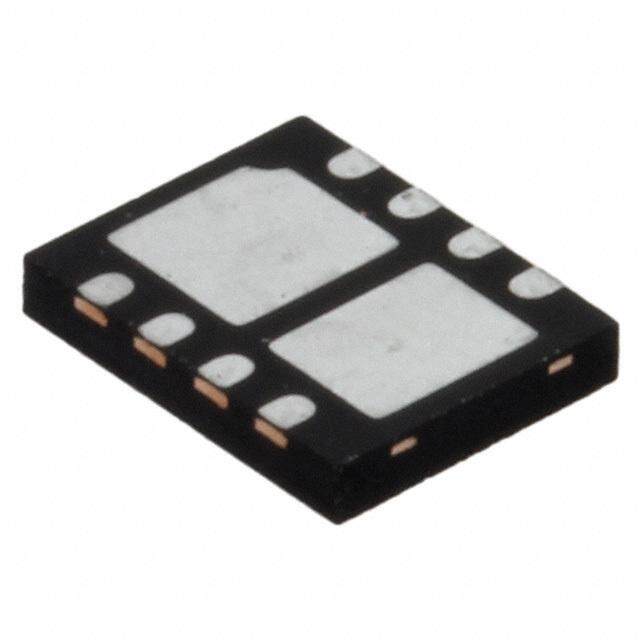
ICGOO电子元器件商城为您提供TPS54383PWPR由Texas Instruments设计生产,在icgoo商城现货销售,并且可以通过原厂、代理商等渠道进行代购。 TPS54383PWPR价格参考。Texas InstrumentsTPS54383PWPR封装/规格:PMIC - 稳压器 - DC DC 开关稳压器, 可调式 降压 开关稳压器 IC 正 0.8V 2 输出 3A 14-TSSOP(0.173",4.40mm 宽)裸露焊盘。您可以下载TPS54383PWPR参考资料、Datasheet数据手册功能说明书,资料中有TPS54383PWPR 详细功能的应用电路图电压和使用方法及教程。
TPS54383PWPR 是由 Texas Instruments 生产的一款高效同步降压 DC-DC 开关稳压器,具有广泛的应用场景。以下是其主要应用场景:

1. 工业自动化与控制:TPS54383PWPR 适用于各种工业设备,如可编程逻辑控制器(PLC)、分布式控制系统(DCS)和智能传感器等。它能够为这些设备提供稳定可靠的电源,确保系统在恶劣环境下正常运行。

2. 通信基础设施:该芯片常用于基站、路由器、交换机等通信设备中。它能够在宽输入电压范围内高效工作,支持多种输出配置,满足不同模块的供电需求,同时具备良好的电磁兼容性(EMC)性能,减少干扰。

3. 汽车电子系统:在现代汽车中,TPS54383PWPR 可以为车载信息娱乐系统、高级驾驶辅助系统(ADAS)、车身控制模块等提供稳定的电源。其高效率和小尺寸设计有助于节省空间并提高能效。

4. 医疗设备:对于便携式或固定式的医疗仪器,如超声波机、心电图仪等,TPS54383PWPR 能够提供精确且稳定的电源输出,确保测量结果的准确性,并延长电池寿命。

5. 消费类电子产品:在笔记本电脑、平板电脑和其他便携式设备中,这款稳压器可以有效地管理电源,降低功耗,提升用户体验。它还支持快速充电功能,缩短充电时间。

6. 数据中心与服务器:TPS54383PWPR 适用于服务器、存储设备等高性能计算平台,提供高效的电源转换,支持多相供电,以应对高电流负载需求,同时保持系统的稳定性和可靠性。

总之,TPS54383PWPR 凭借其卓越的性能和灵活性,成为众多领域中不可或缺的关键组件。
| 参数 | 数值 |
| 产品目录 | 集成电路 (IC) |
| 描述 | IC REG BUCK ADJ 3A DL 14HTSSOP |
| 产品分类 | |
| 品牌 | Texas Instruments |
| 数据手册 | |
| 产品图片 |
|
| 产品型号 | TPS54383PWPR |
| PWM类型 | 电流模式 |
| rohs | 无铅 / 符合限制有害物质指令(RoHS)规范要求 |
| 产品系列 | - |
| 产品目录页面 | |
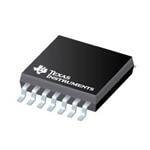
| 供应商器件封装 | 14-HTSSOP |
| 其它名称 | 296-23087-1 |
| 包装 | 剪切带 (CT) |
| 同步整流器 | 无 |
| 安装类型 | 表面贴装 |
| 封装/外壳 | 14-TSSOP (0.173",4.40mm 宽)裸焊盘 |
| 工作温度 | -40°C ~ 125°C |
| 标准包装 | 1 |
| 电压-输入 | 4.5 V ~ 28 V |
| 电压-输出 | 0.8 V ~ 25.2 V |
| 电流-输出 | 3A |
| 类型 | 降压(降压) |
| 输出数 | 2 |
| 输出类型 | 可调式 |
| 配用 | /product-detail/zh/TPS54383EVM/296-31197-ND/1907910 |
| 频率-开关 | 300kHz |


- 商务部:美国ITC正式对集成电路等产品启动337调查
- 曝三星4nm工艺存在良率问题 高通将骁龙8 Gen1或转产台积电
- 太阳诱电将投资9.5亿元在常州建新厂生产MLCC 预计2023年完工
- 英特尔发布欧洲新工厂建设计划 深化IDM 2.0 战略
- 台积电先进制程称霸业界 有大客户加持明年业绩稳了
- 达到5530亿美元!SIA预计今年全球半导体销售额将创下新高
- 英特尔拟将自动驾驶子公司Mobileye上市 估值或超500亿美元
- 三星加码芯片和SET,合并消费电子和移动部门,撤换高东真等 CEO
- 三星电子宣布重大人事变动 还合并消费电子和移动部门
- 海关总署:前11个月进口集成电路产品价值2.52万亿元 增长14.8%


PDF Datasheet 数据手册内容提取
Product Sample & Technical Tools & Support & Folder Buy Documents Software Community TPS54383,TPS54386 SLUS774C–AUGUST2007–REVISEDDECEMBER2014 TPS5438x Dual 3-A Non-Synchronous Converters With Integrated High-Side MOSFET 1 Features 3 Description • 4.5-Vto28-VInputRange The TPS54383 and TPS54386 are dual output, non- 1 synchronous buck converters capable of supporting • OutputVoltageRange0.8Vto90%ofInput 3-A output applications that operate from a 4.5-V to Voltage 28-V input supply voltage, and require output • OutputCurrentUpto3A voltagesbetween0.8Vand90%oftheinputvoltage. • TwoFixedSwitchingFrequencyVersions: With an internally-determined operating frequency, – TPS54383:300kHz soft-start time, and control loop compensation, these converters provide many features with a minimum of – TPS54386:600kHz external components. Channel 1 overcurrent • ThreeSelectableLevelsofOvercurrentProtection protectionissetat4.5A,whileChannel2overcurrent (Output2) protection level is selected by connecting a pin to • 0.8-V1.5%VoltageReference ground, to BP, or left floating. The setting levels are used to allow for scaling of external components for • 2.1-msInternalSoft-Start applicationsthatdonotneedthefullloadcapabilityof • DualPWMOutputs180° Out-of-Phase bothoutputs. • RatiometricorSequentialStartupModes The outputs may be enabled independently, or may SelectablebyaSinglePin beconfiguredtoalloweitherratio-metricorsequential • 85-mΩ InternalHigh-SideMOSFETs startup sequencing. Additionally, the two outputs may • CurrentModeControl bepoweredfromdifferentsources. • InternalCompensation(SeePage16) DeviceInformation(1) • Pulse-by-PulseOvercurrentProtection PARTNUMBER PACKAGE BODYSIZE(NOM) • ThermalShutdownProtectionat+148°C TPS54383 • 14-Pin PowerPAD™HTSSOPpackage HTSSOP(14) 4.40mm×5.00mm TPS54386 2 Applications (1) For all available packages, see the orderable addendum at theendofthedatasheet. • SetTopBox • DigitalTV • PowerforDSP • ConsumerElectronics 4 Simplified Schematic V IN TPS54383 1 PVDD1 PVDD2 14 2 BOOT1 BOOT2 13 OUTPUT1 OUTPUT2 3 SW1 SW2 12 4 GND BP 11 5 EN1 SEQ 10 6 EN2 ILIM2 9 7 FB1 FB2 8 GND UDG-07123 1 An IMPORTANT NOTICE at the end of this data sheet addresses availability, warranty, changes, use in safety-critical applications, intellectualpropertymattersandotherimportantdisclaimers.PRODUCTIONDATA.
TPS54383,TPS54386 SLUS774C–AUGUST2007–REVISEDDECEMBER2014 www.ti.com Table of Contents 1 Features.................................................................. 1 8.4 DeviceFunctionalModes........................................29 2 Applications........................................................... 1 9 ApplicationsandImplementation...................... 30 3 Description............................................................. 1 9.1 ApplicationInformation............................................30 4 SimplifiedSchematic............................................. 1 9.2 TypicalApplications................................................30 5 RevisionHistory..................................................... 2 10 PowerSupplyRecommendations..................... 41 6 PinConfigurationandFunctions......................... 3 11 Layout................................................................... 41 11.1 LayoutGuidelines.................................................41 7 Specifications......................................................... 5 11.2 LayoutExample....................................................42 7.1 AbsoluteMaximumRatings .....................................5 11.3 PowerPADPackage..............................................43 7.2 ESDRatings ............................................................5 12 DeviceandDocumentationSupport................. 44 7.3 RecommendedOperatingConditions.......................5 7.4 ThermalInformation..................................................5 12.1 DeviceSupport......................................................44 7.5 ElectricalCharacteristics...........................................6 12.2 DocumentationSupport........................................45 7.6 TypicalCharacteristics..............................................8 12.3 RelatedLinks........................................................45 12.4 Trademarks...........................................................45 8 DetailedDescription............................................ 11 12.5 ElectrostaticDischargeCaution............................45 8.1 Overview.................................................................11 12.6 Glossary................................................................45 8.2 FunctionalBlockDiagram.......................................12 13 Mechanical,Packaging,andOrderable 8.3 FeatureDescription.................................................13 Information........................................................... 46 5 Revision History ChangesfromRevisionB(October2007)toRevisionC Page • AddedESDRatingstable,FeatureDescriptionsection,DeviceFunctionalModes,ApplicationandImplementation section,PowerSupplyRecommendationssection,Layoutsection,DeviceandDocumentationSupportsection,and Mechanical,Packaging,andOrderableInformationsection.................................................................................................. 1 2 SubmitDocumentationFeedback Copyright©2007–2014,TexasInstrumentsIncorporated ProductFolderLinks:TPS54383 TPS54386
TPS54383,TPS54386 www.ti.com SLUS774C–AUGUST2007–REVISEDDECEMBER2014 6 Pin Configuration and Functions PWPPackage 14-PinHTSSOP BottomView PVDD1 1 14 PVDD2 BOOT1 2 13 BOOT2 SW1 3 12 SW2 ThermalPad GND 4 11 BP (bottomside) EN1 5 10 SEQ EN2 6 9 ILIM2 FB1 7 8 FB2 PinFunctions PIN I/O DESCRIPTION NAME NO. InputsupplytothehighsidegatedriverforOutput1.Connecta22-nFto82-nFcapacitorfromthispin toSW1.ThiscapacitorischargedfromtheBPpinvoltagethroughaninternalswitch.Theswitchis BOOT1 2 I turnedONduringtheOFFtimeoftheconverter.ToslowdowntheturnONoftheinternalFET,asmall resistor(1Ωto3Ω)maybeplacedinserieswiththebootstrapcapacitor. InputsupplytothehighsidegatedriverforOutput2.Connecta22-nFto82-nFcapacitorfromthispin toSW2.ThiscapacitorischargedfromtheBPpinvoltagethroughaninternalswitch.Theswitchis BOOT2 13 I turnedONduringtheOFFtimeoftheconverter.ToslowdowntheturnONoftheinternalFET,asmall resistor(1Ωto3Ω)maybeplacedinserieswiththebootstrapcapacitor. Regulatedvoltagetochargethebootstrapcapacitors.BypassthispintoGNDwithalowESR(4.7-μF BP 11 - to10-μFX7RorX5R)ceramiccapacitor. ActivelowenableinputforOutput1.Ifthevoltageonthispinisgreaterthan1.55V,Output1is disabled(high-sideswitchisOFF).Avoltageoflessthan0.9VenablesOutput1andallowssoft-start EN1 5 I ofOutput1tobegin.AninternalcurrentsourcedrivesthispintoPVDD2ifleftfloating.Connectthispin toGNDfor"alwaysON"operation. ActivelowenableinputforOutput2.Ifthevoltageonthispinisgreaterthan1.55V,Output2is disabled(high-sideswitchisOFF).Avoltageoflessthan0.9VenablesOutput2andallowssoft-start EN2 6 I ofOutput2tobegin.AninternalcurrentsourcedrivesthispintoPVDD2ifleftfloating.Connectthispin toGNDfor"alwaysON"operation. VoltagefeedbackpinforOutput1.TheinternaltransconductanceerroramplifieradjuststhePWMfor Output1toregulatethevoltageatthispintotheinternal0.8-Vreference.Aseriesresistordividerfrom FB1 7 I Output1toground,withthecenterconnectiontiedtothispin,determinesthevalueoftheregulated outputvoltage.Compensationforthefeedbackloopisprovidedinternallytothedevice.SeeFeedback LoopandInductor-Capacitor(L-C)FilterSelectionsectionforfurtherinformation. VoltagefeedbackpinforOutput2.TheinternaltransconductanceerroramplifieradjuststhePWMfor Output2toregulatethevoltageatthispintotheinternal0.8-Vreference.Aseriesresistordividerfrom FB2 8 I Output2toground,withthecenterconnectiontiedtothispin,determinesthevalueoftheregulated Outputvoltage.Compensationforthefeedbackloopisprovidedinternallytothedevice.SeeFeedback LoopandInductor-Capacitor(L-C)FilterSelectionsectionforfurtherinformation. GND 4 - Groundpinforthedevice.ConnectdirectlytoThermalPad. Copyright©2007–2014,TexasInstrumentsIncorporated SubmitDocumentationFeedback 3 ProductFolderLinks:TPS54383 TPS54386
TPS54383,TPS54386 SLUS774C–AUGUST2007–REVISEDDECEMBER2014 www.ti.com PinFunctions(continued) PIN I/O DESCRIPTION NAME NO. CurrentlimitadjustpinforOutput2only.Thisfunctionisintendedtoallowauserwithasymmetrical loadcurrents(Output1loadcurrentmuchgreaterthanOutput2loadcurrent)tooptimizecomponent ILIM2 9 I scalingofthelowercurrentoutputwhilemaintainingpropercomponentderatinginaovercurrentfault condition.ThediscretelevelsareavailableasshowninTable2.Note:Aninternal2-resistordivider (150-kΩeach)connectsBPtoILIM2andtoGND. PowerinputtotheOutput1highsideMOSFETonly.ThispinshouldbelocallybypassedtoGNDwitha PVDD1 1 I lowESRceramiccapacitorof10-μForgreater. ThePVDD2pinprovidespowertothedevicecontrolcircuitry,providesthepull-upfortheEN1andEN2 pinsandprovidespowertotheOutput2high-sideMOSFET.Thispinshouldbelocallybypassedto PVDD2 14 I GNDwithalowESRceramiccapacitorof10-μForgreater.TheUVLOfunctionmonitorsPVDD2and enablesthedevicewhenPVDD2isgreaterthan4.1V. Thispinconfigurestheoutputstartupmode.IftheSEQpinisconnectedtoBP,thenwhenOutput2is enabled,Output1isallowedtostartafterOutput2hasreachedregulation;thatis,sequentialstartup whereOutput1isslavetoOutput2.IfEN2isallowedtogohighaftertheoutputshavebeenoperating, thenbothoutputsaredisabledimmediately,andtheoutputvoltagesdecayaccordingtotheloadthatis present.Forthissequenceconfiguration,tieEN1toground. IftheSEQpinisconnectedtoGND,thenwhenOutput1isenabled,Output2isallowedtostartafter Output1hasreachedregulation;thatis,sequentialstartupwhereOutput2isslavetoOutput1.IfEN1 isallowedtogohighaftertheoutputshavebeenoperating,thenbothoutputsaredisabledimmediately, SEQ 10 I andtheoutputvoltagesdecayaccordingtotheloadthatispresent.Forthissequenceconfiguration,tie EN2toground. Ifleft floating,Output1 andOutput2 startratio-metricallywhenbothoutputsareenabledatthesame time. They will soft-start at a rate determined by their final output voltage and enter regulation at the same time. If the EN1 and EN2 pins are allowed to operate independently, then the two outputs also operateindependently NOTE:Aninternaltworesistor(150-kΩeach)dividerconnectsBPtoSEQandtoGND.Seethe SequenceStatestable. Source(switching)outputforOutput1PWM.Asnubberisrecommendedtoreduceringingonthis SW1 3 O node.SeeSWNodeRingingforfurtherinformation. Source(switching)outputforOutput2PWM.Asnubberisrecommendedtoreduceringingonthis SW2 12 O node.SeeSWNodeRingingforfurtherinformation. ThermalPad — — ThispadmustbetiedexternallytoagroundplaneandtheGNDpin. 4 SubmitDocumentationFeedback Copyright©2007–2014,TexasInstrumentsIncorporated ProductFolderLinks:TPS54383 TPS54386
TPS54383,TPS54386 www.ti.com SLUS774C–AUGUST2007–REVISEDDECEMBER2014 7 Specifications 7.1 Absolute Maximum Ratings(1) MIN MAX UNIT PVDD1,PVDD2,EN1,EN2 30 BOOT1,BOOT2 VSW+7 SW1,SW2 –2 30 Inputvoltagerange SW1,SW2transient(<50ns) –3 31 V BP 6.5 SEQ,ILIM2 –0.3 6.5 FB1,FB2 –0.3 3 SW1,SW2outputcurrent 7 A BPloadcurrent 35 mA TJ Operatingtemperature –40 +150 °C Solderingtemperature +260 Tstg Storagetemperature –55 165 °C (1) PermanentdevicedamagemayoccurifAbsoluteMaximumRatingsareexceeded.Functionaloperationshouldbelimitedtothe RecommendedDCOperatingConditionsdetailedinthisdatasheet.Exposuretoconditionsbeyondtheoperationallimitsforextended periodsoftimemayaffectdevicereliability. 7.2 ESD Ratings VALUE UNIT Human-bodymodel(HBM),perANSI/ESDA/JEDECJS-001(1) ±2000 V(ESD) Electrostaticdischarge Charged-devicemodel(CDM),perJEDECspecificationJESD22- ±1500 V C101(2) (1) JEDECdocumentJEP155statesthat500-VHBMallowssafemanufacturingwithastandardESDcontrolprocess. (2) JEDECdocumentJEP157statesthat250-VCDMallowssafemanufacturingwithastandardESDcontrolprocess. 7.3 Recommended Operating Conditions MIN MAX UNIT VPVDD2 Inputvoltage 4.5 28 V Operatingjunction TJ temperature –40 +125 °C 7.4 Thermal Information TPS54383 TPS54386 THERMALMETRIC(1) UNIT HTSSOP 14PINS R Junction-to-ambientthermalresistance 48.6 θJA R Junction-to-case(top)thermalresistance 29.4 θJC(top) R Junction-to-boardthermalresistance 25.1 θJB °C/W ψ Junction-to-topcharacterizationparameter 0.9 JT ψ Junction-to-boardcharacterizationparameter 24.9 JB R Junction-to-case(bottom)thermalresistance 2.4 θJC(bot) (1) Formoreinformationabouttraditionalandnewthermalmetrics,seetheICPackageThermalMetricsapplicationreport,SPRA953. Copyright©2007–2014,TexasInstrumentsIncorporated SubmitDocumentationFeedback 5 ProductFolderLinks:TPS54383 TPS54386
TPS54383,TPS54386 SLUS774C–AUGUST2007–REVISEDDECEMBER2014 www.ti.com 7.5 Electrical Characteristics –40°C≤T ≤+125°C,V =V =12V,unlessotherwisenoted. J PVDD1 PVDD2 PARAMETER TESTCONDITIONS MIN TYP MAX UNIT INPUTSUPPLY(PVDD) VPVDD1 Inputvoltagerange 4.5 28 V VPVDD2 IDDSDN Shutdown VEN1=VEN2=VPVDD2 70 150 μA IDDQ Quiescent,non-switching VFB=0.9V,Outputsoff 1.8 3.0 SWnodeunloaded;MeasuredasBPsink mA IDDSW Quiescent,while-switching current 5 VUVLO Minimumturn-onvoltage PVDD2only 3.8 4.1 4.4 V VUVLO(hys) Hysteresis 400 mV tSTART(1)(2) Timefromstartuptosoftstartbegin CsiBmPu=lta1n0eμoFus,lEyN1andEN2golow 2 ms ENABLE(EN) VEN1 Enablethreshold 0.9 1.2 1.5 V VEN2 Hysteresis 50 mV IEN1 Enablepull-upcurrent VEN1=VEN2=0V 6 12 μA IEN2 tEN(1) Timefromenabletosoft-startbegin OtherENpin=GND 10 μs BPREGULATOR(BP) BP Regulatorvoltage 8V<PVDD2<28V 5 5.25 5.6 V BPLDO Dropoutvoltage PBVPDD2=4.5V;switching,noexternalloadon 400 mV IBP(1) Regulatorexternalload 2 mA IBPS Regulatorshortcircuit 4.5V<PVDD2<28V 10 20 30 OSCILLATOR TPS54383 255 310 375 fSW Switchingfrequency kHz TPS54386 510 630 750 tDEAD(1) Clockdeadtime 140 ns ERRORAMPLIFIER(EA)andVOLTAGEREFERENCE(REF) VFB1 0°C<TJ<+85°C 788 800 812 Feedbackinputvoltage mV VFB2 –40°C<TJ<+125°C 786 812 IFB1 Feedbackinputbiascurrent 3 50 nA IFB2 gM1(1) Transconductance 30 μS gM2(1) SOFT-START(SS) TSS1 Soft-starttime 1.5 2.1 2.7 ms TSS2 OVERCURRENTPROTECTION ICL1 Currentlimitchannel1 3.6 4.5 5.6 VILIM2=VBP 3.6 4.5 5.6 A ICL2 Currentlimitchannel2 VILIM2=(floating) 2.4 3.0 3.6 VILIM2=GND 1.15 1.50 1.75 VUV1 Low-leveloutputthresholdtodeclareafault Measuredatfeedbackpin. 670 mV VUV2 THICCUP(1) Hiccuptimeout 10 ms tON1(oc)(1) Minimumovercurrentpulsewidth 90 150 ns tON2(oc)(1) (1) Ensuredbydesign.Notproductiontested. (2) Whenbothoutputsarestartedsimultaneously,a20-mAcurrentsourcechargestheBPcapacitor.Fastertimesarepossiblewithalower BPcapacitorvalue.MoreinformationcanbefoundintheInputUVLOandStartupsection. 6 SubmitDocumentationFeedback Copyright©2007–2014,TexasInstrumentsIncorporated ProductFolderLinks:TPS54383 TPS54386
TPS54383,TPS54386 www.ti.com SLUS774C–AUGUST2007–REVISEDDECEMBER2014 Electrical Characteristics (continued) –40°C≤T ≤+125°C,V =V =12V,unlessotherwisenoted. J PVDD1 PVDD2 PARAMETER TESTCONDITIONS MIN TYP MAX UNIT BOOTSTRAP RBOOT1 FromBPtoBOOT1orBPtoBOOT2, Bootstrapswitchresistance 18 Ω RBOOT2 IEXT=50mA OUTPUTSTAGE(Channel1andChannel2) RDS(on)(1) MOSFETonresistanceplusbondwireresistance TJ=+25°C,VPVDD2=8V 85 mΩ –40°C<TJ<+125°C,VPVDD2=8V 85 165 tON(min)(1) Minimumcontrollablepulsewidth ISWxpeakcurrent>1A(3) 100 200 ns DMIN MinimumDutyCycle VFB=0.9V 0 % TPS54383 fSW=300kHz 90 95 % DMAX MaximumDutyCycle TPS54386 fSW=600kHz 85 90 % ISW Switchingnodeleakagecurrent(sourcing) OutputsOFF 2 12 μA THERMALSHUTDOWN TSD(1) Shutdowntemperature 148 °C TSD(hys)(1) Hysteresis 20 (3) SeeFigure14forI peakcurrent<1A. SWx Copyright©2007–2014,TexasInstrumentsIncorporated SubmitDocumentationFeedback 7 ProductFolderLinks:TPS54383 TPS54386
TPS54383,TPS54386 SLUS774C–AUGUST2007–REVISEDDECEMBER2014 www.ti.com 7.6 Typical Characteristics 2.1 140 VBP=5.25 V VPVDDx=28 V 120 2.0 VPVDDx=12 V -Quiescent CurrentmA 111...798 -mShutdown CurrentA 1680000 - - 40 IDDQ 1.6 ISD 20 VPVDDx=4.5 V 1.5 0 -50 -25 0 25 50 75 100 125 -50 -25 0 25 50 75 100 125 TJ-Junction Temperature-°C TJ-Junction Temperature-°C Figure1.QuiescentCurrent(Non-Switching)vsJunction Figure2.ShutdownCurrentvsJunctionTemperature Temperature 4.2 1.25 EN(Off) --VUndervoltage LockoutVUVLO 33344.....78910 UUVVLLOO((OOfnf)) --VEnable Threshold VoltageVEN1111....12217139 EN(On) 3.6 1.15 -50 -25 0 25 50 75 100 125 -50 -25 0 25 50 75 100 125 TJ-Junction Temperature-°C TJ-Junction Temperature-°C Figure3.UndervoltageLockoutThresholdvsJunction Figure4.EnableThresholdsvsJunctionTemperature Temperature 3.5 350 VBP=5.25 V VBP=5.25 V ms 3.0 kHz 330 -Soft Start Time 2.5 -PWM Frequency 310 - - tSS 2.0 fPWM290 1.5 270 -50 -25 0 25 50 75 100 125 -50 -25 0 25 50 75 100 125 TJ-Junction Temperature-°C TJ-Junction Temperature-°C Figure5.Soft-StartTimevsJunctionTemperature Figure6.SwitchingFrequency(300kHz)vsJunction Temperature 8 SubmitDocumentationFeedback Copyright©2007–2014,TexasInstrumentsIncorporated ProductFolderLinks:TPS54383 TPS54386
TPS54383,TPS54386 www.ti.com SLUS774C–AUGUST2007–REVISEDDECEMBER2014 Typical Characteristics (continued) 680 5 VBP=5.25 V 660 A 3 --fPWM FrequencykHzPWM666042000 --IFeedback Bias CurrentnFB --131 580 -5 -50 -25 0 25 50 75 100 125 -50 -25 0 25 50 75 100 125 TJ-Junction Temperature-°C TJ-Junction Temperature-°C Figure7.SwitchingFrequency(600kHz)vsJunction Figure8.FeedbackBiasCurrentvsJunctionTemperature Temperature 808 4.8 VPVDD=24 V mV 803 A 4.6 --VFeedback VoltageFB779938 --IOvercurrent LimitCL44..42 VPVDD=5 V VPVDD=12 V 788 4.0 -50 -25 0 25 50 75 100 125 -50 -25 0 25 50 75 100 125 TJ-Junction Temperature-°C TJ-Junction Temperature-°C Figure9.FeedbackVoltagevsJunctionTemperature Figure10.OvercurrentLimit(CH1,CH2HighLevel)vs JunctionTemperature 3.4 1.8 VPVDDx=24 V VPVDDx=24 V A 3.2 A -mit -mit 1.6 Overcurrent Li 3.0 Overcurrent Li 1.4 - - ICL2.8 ICL VPVDDx=12 V VPVDDx=5 V VPVDDx=12 V VPVDDx=5 V 2.6 1.2 -50 -25 0 25 50 75 100 125 -50 -25 0 25 50 75 100 125 TJ-Junction Temperature-°C TJ-Junction Temperature-°C Figure11.OvercurrentLimit(CH2MidLevel)vsJunction Figure12.OvercurrentLimit(CH2LowLevel)vsJunction Temperature Temperature Copyright©2007–2014,TexasInstrumentsIncorporated SubmitDocumentationFeedback 9 ProductFolderLinks:TPS54383 TPS54386
TPS54383,TPS54386 SLUS774C–AUGUST2007–REVISEDDECEMBER2014 www.ti.com Typical Characteristics (continued) 5 400 -SwitchingNodeLeakageCurrent-AmW(off) 234 -MinimumControllablePulseWidth-nsON223311050505000000 TA=25°CTAT=A–4=00°°CC TA(°–028C455)0 IS t TA=85°C 1 50 -50 -25 0 25 50 75 100 125 0 0.2 0.4 0.6 0.8 1.0 1.2 1.4 TJ-JunctionTemperature-°C IL-LoadCurrent-A Figure14.MinumumControllablePulseWidthvsLoad Figure13.SwitchingNodeLeakageCurrentvsJunction Current Temperature 5.0 4.5 A 4.0 Limit- 3.5 OCL=3.0A OCL=4.5A Overcurrent 23..50 I-OC2.0 OCL=1.5A 1.5 1.0 4 8 12 16 20 24 28 VDD-SupplyVoltage-V Figure15.OvercurrentLimitvsSupplyVoltage 10 SubmitDocumentationFeedback Copyright©2007–2014,TexasInstrumentsIncorporated ProductFolderLinks:TPS54383 TPS54386
TPS54383,TPS54386 www.ti.com SLUS774C–AUGUST2007–REVISEDDECEMBER2014 8 Detailed Description 8.1 Overview The TPS54383 and TPS54386 are dual output, non-synchronous step down (buck) converters. Integrated into each PWM channel is an internally-compensated error amplifier, current mode pulse width modulator (PWM), switch MOSFET, internal bootstrap switch for high-side gate drive, and fault protection circuitry. Each channel also contains an EN pin and internal fixed soft-start time. The fault protection circuitry includes cycle-by-cycle current limit, output undervoltage detection, hiccup timeout and thermal shutdown. Channel 1 has a fixed current limit and channel 2 has three selectable overcurrent levels. Common to the two channels is the internal BP voltageregulator,voltagereference,clockoscillator,andoutputvoltagesequencingfunctions. DESIGNHINT The TPS5438x contains internal slope compensation and loop compensation components; therefore,theexternalL-Cfiltermustbeselectedappropriatelysothattheresultingcontrol loop meets criteria for stability. This approach differs from an externally-compensated controller, where the L-C filter is generally selected first, and the compensation network is foundafterwards.(SeeFeedbackLoopandL-CFilterSelection section.) NOTE Unless otherwise noted, the term TPS5438x applies to both the TPS54383 and TPS54386. Also, unless otherwise noted, a label with a lowercase x appended implies the term applies to both outputs of the two modulator channels. For example, the term ENx implies both EN1 and EN2. Unless otherwise noted, all parametric values given are typical. Refer to the Electrical Characteristics for minimum and maximum values. Calculationsshouldbeperformedwithtolerancevaluestakenintoconsideration. Copyright©2007–2014,TexasInstrumentsIncorporated SubmitDocumentationFeedback 11 ProductFolderLinks:TPS54383 TPS54386
TPS54383,TPS54386 SLUS774C–AUGUST2007–REVISEDDECEMBER2014 www.ti.com 8.2 Functional Block Diagram 2 BOOT1 BP CLK1 Level 1 PVDD1 Shift Current f(I )+DC(ofst) Comparator DRAIN1 S Q + GND 4 R R Q + f(I ) FB1 7 DRAIN1 OvercurrentComp 0.8V + 3 SW1 REF RCOMP f(ISLOPE1) f(IMAX1) BP SoftStart Weak SD1 1 CCOMP CLK1 Anti-Cross Pull-Down Conduction MOSFET VDD2 f(I ) SLOPE1 Ramp Gen1 TSD 1.2MHz Divide CLK1 6mA 6mA Oscilator by2/4 f(I ) SLOPE2 EN1 5 SD1 Ramp Gen2 Internal SD2 EN2 6 Control CLK2 UVLO 150kW SEQ 10 BP FB1 Output Undervoltage 150kW 13 BOOT2 FB2 Detect BP CLK2 Level 14 PVDD2 Shift Current Comparator FET f(I )+DC(ofst) DRAIN2 S Q Switch + GND 4 R R Q + f(I ) FB2 8 DRAIN2 OvercurrentComp 0.8V + 12 SW2 REF RCOMP f(ISLOPE2) f(IMAX2) BP SoftStart Weak SD2 2 CCOMP CLK2 Anti-Cross Pull-Down Conduction MOSFET 5.25-V BP 11 PVDD2 Regulator 150kW BP Level ILIM2 9 Select 150kW 0.8V REF References I (Settooneofthreelimits) MAX2 UDG-07124 12 SubmitDocumentationFeedback Copyright©2007–2014,TexasInstrumentsIncorporated ProductFolderLinks:TPS54383 TPS54386
TPS54383,TPS54386 www.ti.com SLUS774C–AUGUST2007–REVISEDDECEMBER2014 8.3 Feature Description 8.3.1 VoltageReference Thebandgapcellcommontobothoutputs,trimmedto800mV. 8.3.2 Oscillator The oscillator frequency is internally fixed at two times the SWx node switching frequency. The two outputs are internallyconfiguredtooperateonalternatingswitchcycles(thatis,180° outofphase). 8.3.3 InputUndervoltageLockout(UVLO)andStartup When the voltage at the PVDD2 pin is less than 4.1 V, a portion of the internal bias circuitry is operational, and all other functions are held OFF. All of the internal MOSFETs are also held OFF. When the PVDD2 voltage rises above the UVLO turn-on threshold, the state of the enable pins determines the remainder of the internal startup sequence. If either output is enabled (ENx pulled low), the BP regulator turns on, charging the BP capacitor with a 20-mA current. When the BP pin is greater than 4 V, PWM is enabled and soft-start begins, depending on the SEQmodeofoperationandthe EN1andEN2settings. Note that the internal regulator and control circuitry are powered from PVDD2. The voltage on PVDD1 may be higherorlowerthanPVDD2.(SeetheDualSupplyOperationsection.) 8.3.4 EnableandTimedTurnOnoftheOutputs Each output has a dedicated (active low) enable pin. If left floating, an internal current source pulls the pin to PVDD2. By grounding, or by pulling the ENx pin to below approximately 1.2 V with an external circuit, the associatedoutputisenabledandsoft-startisinitiated. If both enable pins are left in the high state, the device operates in a shutdown mode, where the BP regulator is shut down and minimal functions are active. The total standby current from both PVDD pins is approximately 70 μAat12-Vinputsupply. An R-C connected to an ENx pin may be used to delay the turn-on of the associated output after power is applied to PVDDx (see Figure 16). After power is applied to PVDD2, the voltage on the ENx pin slowly decays towards ground. Once the voltage decays to approximately 1.2 V, then the output is enabled and the startup sequence begins. If it is desired to enable the outputs of the device immediately upon the application of power to PVDD2,thenomitthesetwocomponentsandtiethe ENxpintoGNDdirectly. If an R-C circuit is used to delay the turn-on of the output, the resistor value must be much less than 1.2 V / 6μA or 200 kΩ. A suggested value is 51 kΩ. This resistor value allows the ENx voltage to decay below the 1.2-V thresholdwhilethe6-μAbiascurrentflows. Thecapacitorvaluerequiredtodelaythestartuptime(aftertheapplicationofPVDD2)isshowninEquation1. t C= DELAY farads æV -2´I ´Rö R´lnç IN ENx ÷ è VTH-IENx´R ø where: • RandCarethetimingcomponents • V isthe1.2-Venablethresholdvoltage TH • I isthe6μAenablepinbiasingcurrent (1) ENx Other enable pin functionality is dictated by the state of the SEQ pin. (See the Output Voltage Sequencing section.) Copyright©2007–2014,TexasInstrumentsIncorporated SubmitDocumentationFeedback 13 ProductFolderLinks:TPS54383 TPS54386
TPS54383,TPS54386 SLUS774C–AUGUST2007–REVISEDDECEMBER2014 www.ti.com Feature Description (continued) PVDD2 6mA C ENx PVDDx PVDDx + 1.2-V Threshold 1.2 V R ENx TPS5438x V OUTx 0 t t + t DELAY DELAY SS T-Time Figure16.StartupDelaySchematic Figure17.StartupDelaywithR-ConEnable DESIGNHINT If delayed output voltage startup is not necessary, simply connect EN1 and EN2 to GND. ThisconfigurationallowstheoutputstostartimmediatelyonvalidapplicationofPVDD2. If ENx is allowed to go high after the Outputx has been in regulation, the upper MOSFET shuts off, and the outputdecaysataratedeterminedbytheoutputcapacitorandtheload.TheinternalpulldownMOSFETremains intheOFFstate.(SeetheBootstrapforN-ChannelMOSFET section.) 8.3.5 OutputVoltageSequencing The TPS5438x allows single-pin programming of output voltage startup sequencing. During power-on, the state of the SEQ pin is detected. Based on whether the pin is tied to BP, to GND, or left floating, the outputs behave asdescribedinTable1. Table1.SequenceStates SEQPINSTATE MODE EN1 EN2 Ignoredbythedevice.whenV < EN2 enablethresholdvoltage TieEN1to<enablethresholdvoltage forBPtobeactivewhenV > BP Sequential,Output2thenOutput1 EN2 Active enablethresholdvoltage TieEN1to>enablethresholdvoltage forlowquiescentcurrent(BPinactive) whenV >enablethresholdvoltage EN2 Ignoredbythedevice.whenV < EN1 enablethresholdvoltage TieEN2to<enablethresholdvoltage forBPtobeactivewhenV > GND Sequential,Output1thenOutput2 Active EN1 enablethresholdvoltage TieEN2to>enablethresholdvoltage forlowquiescentcurrent(BPinactive) whenV >enablethresholdvoltage EN1 IndependentorRatiometric,Output1 Active.EN1andEN2mustbetied Active.EN1andEN2mustbetied (floating) andOutput2 togetherforRatio-metricstartup. togetherforRatio-metricstartup. 14 SubmitDocumentationFeedback Copyright©2007–2014,TexasInstrumentsIncorporated ProductFolderLinks:TPS54383 TPS54386
TPS54383,TPS54386 www.ti.com SLUS774C–AUGUST2007–REVISEDDECEMBER2014 IftheSEQpinisconnectedtoBP,thenwhenOutput2isenabled,Output1isallowedtostartapproximately400 μsafterOutput2hasreachedregulation;thatis,sequentialstartupwhereOutput1isslavetoOutput2.If EN2is allowed to go high after the outputs have been operating, then both outputs are disabled immediately, and the outputvoltagesdecayaccordingtotheloadthatispresent. If the SEQ pin is connected to GND, then when Output 1 is enabled, Output 2 is allowed to start approximately 400 μs after Output 1 has reached regulation; that is, sequential startup where Output 2 is slave to Output 1. If EN1 is allowed to go high after the outputs have been operating, then both outputs are disabled immediately, andtheoutputvoltagesdecayaccordingtotheloadthatispresent. SEQ=BP SEQ=GND Sequential Sequential CH2thenCH1 CH1thenCH2 5-VVOUT1 (2V/div) 5-VVOUT1 (2V/div) 3.3-VVOUT2 (2V/div) 3.3-VVOUT2 (2V/div) T-Time-1ms/div T-Time-1ms/div Figure18.SEQPinTIedtoBP Figure19.SEQPinTiedtoGND NOTE An R-C network connected to the ENx pin may be used in addition to the SEQ pin in sequential mode to delay the startup of the first output voltage. This approach may be necessary in systems with a large number of output voltages and elaborate voltage sequencingrequirements.SeeEnableandTimedTurnOnoftheOutputs. If the SEQ pin is left floating, Output 1 and Output 2 each start ratiometrically when both outputs are enabled at the same time. Output 1 and Output 2 soft-start at a rate that is determined by the respective final output voltages and enter regulation at the same time. If the EN1 and EN2 pins are allowed to operate independently, thenthetwooutputsalsooperateindependently. Copyright©2007–2014,TexasInstrumentsIncorporated SubmitDocumentationFeedback 15 ProductFolderLinks:TPS54383 TPS54386
TPS54383,TPS54386 SLUS774C–AUGUST2007–REVISEDDECEMBER2014 www.ti.com 5-VVOUT1 (2V/div) 3.3-VVOUT2 (2V/div) T-Time-1ms/div Figure20. SEQPinFloating 8.3.6 Soft-Start Each output has a dedicated soft-start circuit. The soft-start voltage is an internal digital reference ramp to one of two noninverting inputs of the error amplifier. The other input is the (internal) precision 0.8-V reference. The total ramp time for the FB voltage to charge from 0 V to 0.8 V is about 2.1 ms. During a soft-start interval, the TPS5438x output slowly increases the voltage to the noninverting input of the error amplifier. In this way, the output voltage ramps up slowly until the voltage on the noninverting input to the error amplifier reaches the internal 0.8 V reference voltage. At that time, the voltage at the noninverting input to the error amplifier remains atthereferencevoltage. NOTE To avoid a disturbance in the output voltage during the stepping of the digital soft -tart, a minimum output capacitance of 50μF is recommended. See Feedback Loop and Inductor- Capacitor (L-C) Filter Selection Once the filter and compensation components have been established, laboratory measurements of the physical design should be performed to confirmconverterstability. During the soft-start interval, pulse-by-pulse current limiting is in effect. If an overcurrent pulse is detected, six PWM pulses are skipped to allow the inductor current to decay before another PWM pulse is applied. (See the OutputOverloadProtection section.)Thereisnopulseskippingifacurrentlimitpulseisnotdetected. DESIGNHINT If the rate of rise of the input voltage (PVDDx) is such that the input voltage is too low to support the desired regulation voltage by the time Soft-Start has completed, then the output UV circuit may trip and cause a hiccup in the output voltage. In this case, use a timed delay startup from the ENx pin to delay the startup of the output until the PVDDx voltage has the capability of supporting the desired regulation voltage. See Operating NearMaximumDutyCycleandMaximumOutputCapacitanceforrelatedinformation. 16 SubmitDocumentationFeedback Copyright©2007–2014,TexasInstrumentsIncorporated ProductFolderLinks:TPS54383 TPS54386
TPS54383,TPS54386 www.ti.com SLUS774C–AUGUST2007–REVISEDDECEMBER2014 8.3.7 OutputVoltageRegulation Each output has a dedicated feedback loop comprised of a voltage setting divider, an error amplifier, a pulse width modulator, and a switching MOSFET. The regulation output voltage is determined by a resistor divider connecting the output node, the FBx pin, and GND (see Figure 21). Assuming the value of the upper voltage setting divider is known, the value of the lower divider resistor for a desired output voltage is calculated by Equation2. V REF R2 = R1´ V -V OUT REF where • V istheinternal0.8-Vreferencevoltage (2) REF TPS5438x 1 PVDD1 PVDD2 14 2 BOOT1 BOOT2 13 OUTPUT1 3 SW1 SW2 12 4 GND BP 11 R1 5 EN1 SEQ 10 6 EN2 ILIM2 9 7 FB1 FB2 8 R2 UDG-07011 Figure21. FeedbackNetworkforChannel1 DESIGNHINT There is a leakage current of up to 12 μA out of the SW pin when a single output of the TPS5438x is disabled. Keeping the series impedance of R1 + R2 less than 50 kΩ prevents the output from floating above the reference voltage while the controller output is intheOFFstate. 8.3.8 FeedbackLoopandInductor-Capacitor(L-C)FilterSelection In the feedback signal path, the output voltage setting divider is followed by an internal g -type error amplifier M with a typical transconductance of 30 μS. An internal series connected R-C circuit from the g amplifier output to M ground serves as the compensation network for the converter. The signal from the error amplifier output is then buffered and combined with a slope compensation signal before it is mirrored to be referenced to the SW node. Here, it is compared with the current feedback signal to create a pulse-width-modulated (PWM) signal-fed to drivetheupperMOSFETswitch.AsimplifiedequivalentcircuitofthesignalcontrolpathisdepictedinFigure22. NOTE NoisecouplingfromtheSWxnodetointernalcircuitryofBOOTxmayimpactnarrowpulse width operation, especially at load currents less than 1 A. See SW Node Ringing for furtherinformationonreducingnoiseontheSWxnode. Copyright©2007–2014,TexasInstrumentsIncorporated SubmitDocumentationFeedback 17 ProductFolderLinks:TPS54383 TPS54386
TPS54383,TPS54386 SLUS774C–AUGUST2007–REVISEDDECEMBER2014 www.ti.com TPS5438x BOOT I - I COMP SLOPE x2 PWM to ErrorAmplifier I Switch SLOPE 0.8 V + REF + I FB COMP Offset f(I ) DRAIN R COMP SW 11.5 kW C COMP R C COMP COMP (kW) (pF) TPS54383 700 40 TPS54386 700 20 UDG-07012 Figure22. FeedbackLoopEquivalentCircuit A more conventional small signal equivalent block diagram is shown in Figure 23. Here, the full closed loop signal path is shown. Because the TPS5438x contains internal slope compensation and loop compensation components,theexternalL-Cfiltermustbeselectedappropriatelysothattheresultingcontrolloopmeetscriteria for stability. This approach differs from an externally-compensated controller, where the L-C filter is generally selected first, and the compensation network is found afterwards. To find the appropriate L and C filter combination, the Output-to-Vc signal path plots (see the next section) of gain and phase are used along with otherdesigncriterialtoaidinfindingthecombinationsthatbestresultsinastablefeedbackloop. VIN V + C + VOUT VREF Modulator _ _ Filter Current Feedback Network Compensation Network Figure23. SmallSignalEquivalentBlockDiagram 8.3.9 Inductor-Capacitor(L-C)Selection The following figures plot the TPS5438x Output-to-Vc gain and phase versus frequency for various duty cycles (10%, 30%, 50%, 70%, 90%) at three (200 mA, 400 mA, 600 mA) peak-to-peak ripple current levels. The loop response curve selected to compensate the loop is based on the duty cycle of the application and the ripple current in the inductor. Once the curve has been selected and the inductor value has been calculated, the output capacitor is found by calculating the L-C resonant frequency required to compensate the feedback loop. A brief examplefollowsthecurves. Note that the internal error amplifier compensation is optimized for output capacitors with an ESR zero frequency between20kHzand60kHz.Seethefollowingsectionsforfurtherdetails. 18 SubmitDocumentationFeedback Copyright©2007–2014,TexasInstrumentsIncorporated ProductFolderLinks:TPS54383 TPS54386
TPS54383,TPS54386 www.ti.com SLUS774C–AUGUST2007–REVISEDDECEMBER2014 100 270 100 270 DutyCycle% DutyCycle% Gain Phase 225 Gain Phase 225 80 10 80 10 30 30 50 180 50 180 70 70 60 90 60 90 135 135 B ° B d - d ° ain- 40 90 hase ain- 40 90 ase- G P G h P 45 45 20 20 0 0 0 0 -45 -45 -20 -90 -20 -90 100 1k 10k 100k 1M 100 1k 10k 100k 1M f-Frequency-Hz Figure25.GainandPhasevsFrequency.TPS54383at Figure24.GainandPhasevsFrequency.TPS54383at 400-mAppRippleCurrent 200-mAppRippleCurrent 100 270 100 270 DutyCycle% 85 225 Gain Phase 225 80 10 30 70 180 50 180 70 60 90 135 55 135 dB -° dB -° ain- 40 90 hase -ain 40 90 hase G P G P 45 25 45 20 Duty Cycle % 0 10 Gain Phase 0 10 0 30 -45 -5 50 -45 70 90 -20 -90 -20 -90 100 1k 10k 100k 1M f-Frequency-Hz 100 1 k 10 k 100 k 1 M f-Frequency-Hz Figure26.GainandPhasevsFrequency.TPS54383at Figure27.GainandPhasevsFrequency.TPS54386at 600-mAppRippleCurrent 200-mAppRippleCurrent Copyright©2007–2014,TexasInstrumentsIncorporated SubmitDocumentationFeedback 19 ProductFolderLinks:TPS54383 TPS54386
TPS54383,TPS54386 SLUS774C–AUGUST2007–REVISEDDECEMBER2014 www.ti.com 100 270 100 270 85 225 225 80 70 180 180 60 135 55 135 ain-dB 40 90 hase-° -aindB 40 90°-ase G P G h P 45 25 45 20 DutyCycle% Duty Cycle % Gain10Phase 0 10 Gain 1 0Phase 0 0 30 30 5700 -45 -5 50 -45 70 90 90 -20 -90 -20 -90 100 1k 10k 100k 1M f-Frequency-Hz 100 1 k 10 k 100 k 1 M f-Frequency-Hz Figure28.GainandPhasevsFrequency.TPS54386at Figure29.GainandPhasevsFrequency.TPS54386at 400-mAppRippleCurrent 600-mAppRippleCurrent 8.3.10 MaximumOutputCapacitance With internal pulse-by-pulse current limiting and a fixed soft-start time, there is a maximum output capacitance which may be used before startup problems begin to occur. If the output capacitance is large enough so that the device enters a current limit protection mode during startup, then there is a possibility that the output will never reach regulation. Instead, the TPS5438x simply shuts down and attempts a restart as if the output were short- circuited to ground. The maximum output capacitance (including bypass capacitance distributed at the load) is givenbyEquation3: R1 V (1+ ) ´T t R1 REF R2 S 1 C = SS I -V (1+ )(1- + ) OUTmax V CLx REF R2 2´V ´L R REF IN LOAD (3) 8.3.11 MinimumOutputCapacitance Ensure the value of capacitance selected for closed loop stability is compatible with the requirements of Soft- Start . 8.3.12 ModifyingTheFeedbackLoop Within the limits of the internal compensation, there is flexibility in the selection of the inductor and output capacitor values. A smaller inductor increases ripple current, and raises the resonant frequency, thereby incerasing the required amount of output capacitance. A smaller capacitor could also be used, increasing the resonant frequency, and increasing the overall loop bandwidth—perhaps at the expense of adequate phase margin. The internal compensation of the TPS54x8x is designed for capacitors with an ESR zero frequency between 20kHz and 60kHz. It is possible, with additional feedback compensation components, to use capacitors with higher or lower ESR zero frequencies. For either case, the components C1 and R3 (ref.Figure 30 ) are added to re-compensate the feedback loop for stability. In this configuration a low frequency pole is followed by a higher frequency zero. The placement of this pole-zero pair is dependent on the type of output capacitor used, and the desiredclosedloopfrequencyresponse. 20 SubmitDocumentationFeedback Copyright©2007–2014,TexasInstrumentsIncorporated ProductFolderLinks:TPS54383 TPS54386
TPS54383,TPS54386 www.ti.com SLUS774C–AUGUST2007–REVISEDDECEMBER2014 TPS5438x 1 PVDD1 PVDD2 14 2 BOOT1 BOOT2 13 OUTPUT1 3 SW1 SW2 12 C2 R1 4 GND BP 11 5 EN1 SEQ 10 C1 6 EN2 ILIM2 9 R2 7 FB1 FB2 8 R3 UDG-07013 Figure30. OptionalLoopCompensationComponents NOTE Once the filter and compensation components have been established, laboratory measurementsofthephysicaldesignshouldbeperformedtoconfirmconverterstability. 8.3.12.1 UsingHigh-ESROutputCapacitors If a high-ESR capacitor is used in the output filter, a zero appears in the loop response that could lead to instability. To compensate, a small R-C series connected network is placed in parallel with the lower voltage setting divider resistor (see Figure 30). The values of the components are determined such that a pole is placed at the same frequency as the ESR zero and a new zero is placed at a frequency location conducive to good loop stability. The value of the resistor is calculated using a ratio of impedances to match the ratio of ESR zero frequency to thedesiredzerofrequency. R2 R3= ææf ö ö çç ZERO(desired) ÷-1÷ çç f ÷ ÷ èè ESR(zero) ø ø where: • f istheESRzerofrequencyoftheoutputcapacitor. ESR(zero) • f isthedesiredfrequencyofthezeroaddedtothefeedback.Thisfrequencyshouldbeplaced ZERO(desired) between20kHzand60kHztoensuregoodloopstability. (4) ThevalueofthecapacitoriscalculatedinEquation5. 1 C1= 2p´R ´f EQ ESR(zero) where: • R isanequivalentimpedancecreatedbytheparallelcombinationofthevoltagesettingdividerresistors(R1 EQ andR2)inserieswithR3. (5) Copyright©2007–2014,TexasInstrumentsIncorporated SubmitDocumentationFeedback 21 ProductFolderLinks:TPS54383 TPS54386
TPS54383,TPS54386 SLUS774C–AUGUST2007–REVISEDDECEMBER2014 www.ti.com 1 R =R3+ EQ ææ 1 ö æ 1 öö çç ÷+ç ÷÷ èèR1ø èR2øø (6) 8.3.12.2 UsingAllCeramicOutputCapacitors With low ESR ceramic capacitors, there may not be enough phase margin at the crossover frequency. In this case, (see Figure 30) resistor R3 is set equal to 1/2 R2. This lowers the gain by 6 dB, reduce the crossover frequency,andimprovephasemargin. The value of C1 is found by determining the frequency to place the low frequency pole. The minimum frequency to place the pole is 1 kHz. Any lower, and the time constant will be too slow and interfere with the internal soft- start (see Soft-Start). The upper bound for the pole frequency is determined by the operating frequency of the converter. It is 3 kHz for the TPS54x83, and 6 kHz for the TPS54x86. C1 is then found from Equation 7. Keep componenttolerancesinmindwhenselectingthedesiredpolefrequency. 1 C1= 2p´R ´f EQ POLE(desired) where: • f isthedesiredpolefrequencybetween1kHzand3kHz(TPS54x83)or1kHzand6kHz POLE(desired) (TPS54x86). • R isanequivalentimpedancecreatedbytheparallelcombinationofthevoltagesettingdividerresistors(R1 EQ andR2)inserieswithR3. (7) 1 R =R3+ EQ ææ 1 ö æ 1 öö çç ÷+ç ÷÷ èèR1ø èR2øø (8) If it is necessary to increase phase margin, place a capacitor in parallel with the upper voltage setting divider resistor(Ref.C2inEquation9). 1 R1 C2= ´ 1+ 2p´fC´R1 æ(R2´R3)ö ç ÷ ç(R2+R3)÷ è ø where • f istheunitygaincrossoverfrequency,(approximately50kHzformostdesignsfollowingtheseguidelines) C (9) 8.3.13 Example:TPS54386BuckConverterOperatingat12-VInput,3.3-VOutputand400-mA Ripple (P-P) Current First, the steady state duty cycle is calculated. Assuming the rectifier diode has a voltage drop of 0.5 V, the duty cycleisapproximatedusingEquation10. V +V 3.3+0.5 OUT DIODE d= = = 30% V +V 12+0.5 IN DIODE (10) Thefilterinductoristhencalculated;seeEquation11. L= VIN-VOUT ´d´TS =12-3.3´0.3´ 1 =10.9mH DIL 0.4 600000 (11) 22 SubmitDocumentationFeedback Copyright©2007–2014,TexasInstrumentsIncorporated ProductFolderLinks:TPS54383 TPS54386
TPS54383,TPS54386 www.ti.com SLUS774C–AUGUST2007–REVISEDDECEMBER2014 A custom-designed inductor may be used for the application, or a standard value close to the calculated value may be used. For this example, a standard 10-μH inductor is used. Using Figure 28, find the 30% duty cycle curve. The 30% duty cycle curve has a down slope from low frequency and rises at approximately 6 kHz. This curve is the resonant frequency that must be compensated. Any frequency wthin an octave of the peak may be usedincalculatingthecapacitorvalue.Inthisexample,6kHzisused. 1 1 C= = =70mF L´(2´p´fRES)2 10´10-6´(2´3.14´6000)2 (12) A 68-μF capacitor should be used as a bulk capacitor, with up to 10 μF of ceramic bypass capacitance. To ensure the ESR zero does not significantly impact the loop response, the ESR of the bulk capacitor should be placedadecadeabovetheresonantfrequency. 1 1 RESR < 2´p´10´fRES´C = 2´3.14´10´6000´68´(10)-6 »40mW (13) The resulting loop gain and phase are shown in Figure 31. Based on measurement, loop crossover is 45 kHz withaphasemarginof60degrees. 80 180 70 Phase 135 60 90 50 45 40 B ° d - -ain 30 0 hase G P 20 -45 10 -90 0 Gain -135 -10 -20 -180 100 1 k 10 k 100 k 1 M f-Frequency-Hz Figure31.GainandPhasevsFrequency.ExampleLoopResult 8.3.14 BootstrapfortheN-ChannelMOSFET A bootstrap circuit provides a voltage source higher than the input voltage and of sufficient energy to fully enhance the switching MOSFET each switching cycle. The PWM duty cycle is limited to a maximum of 90%, allowing an external bootstrap capacitor to charge through an internal synchronous switch (between BP and BOOTx) during every cycle. When the PWM switch is commanded to turn ON, the energy used to drive the MOSFETgateisderivedfromthevoltageonthiscapacitor. To allow the bootstrap capacitor to charge each switching cycle, an internal pulldown MOSFET (from SW to GND) is turned ON for approximately 140 ns at the beginning of each switching cycle. In this way, if, during light load operation, there is insufficient energy for the SW node to drive to ground naturally, this MOSFET forces the SWnodetowardgroundandallowthebootstrapcapacitortocharge. Because this is a charge transfer circuit, care must be taken in selecting the value of the bootstrap capacitor. It must be sized such that the energy stored in the capacitor on a per cycle basis is greater than the gate charge requirementoftheMOSFETbeingused. DESIGNHINT For the bootstrap capacitor, use a ceramic capacitor with a value between 22 nF and 82 nF. Copyright©2007–2014,TexasInstrumentsIncorporated SubmitDocumentationFeedback 23 ProductFolderLinks:TPS54383 TPS54386
TPS54383,TPS54386 SLUS774C–AUGUST2007–REVISEDDECEMBER2014 www.ti.com NOTE For 5-V input applications, connect PVDDx to BP directly. This connection bypasses the internal control circuit regulator and provides maximum voltage to the gate drive circuitry. Inthisconfiguration,shutdownmodeIDD willbethesameasquiescentIDD . SDN Q 8.3.15 LightLoadOperation There is no special circuitry for pulse skipping at light loads. The normal characteristic of a nonsynchronous converter is to operate in the discontinuous conduction mode (DCM) at an average load current less than one- half of the inductor peak-to-peak ripple current. Note that the amplitude of the ripple current is a function of input voltage,outputvoltage,inductorvalue,andoperatingfrequency,asshowninEquation14. V -V 1 IN OUT I = ´ ´ d ´T DCM 2 L S (14) Further, during discontinuous mode operation the commanded pulse width may become narrower than the capability of the converter to resolve. To maintain the output voltage within regulation, skipping switching pulses at light load conditions is a natural by-product of that mode. This condition may occur if the output capacitor is charged to a value greater than the output regulation voltage, and there is insufficient load to discharge the capacitor.Aby-productofpulseskippingisanincreaseinthepeak-to-peakoutputripplevoltage. SWWaveform Skipping SWWaveform V =12V IN V =5V OUT V OUT Ripple RViOppUlTe Inductor Current SteadyState Inductor V =12V IN Current V =5V OUT Figure32.SteadyState Figure33.Skipping DESIGNHINT If additional output capacitance is required to reduce the output voltage ripple during DCM operation,besuretorecheckFeedbackLoopandInductor-Capacitor(L-C)FilterSelection andMaximumOutputCapacitancesections. 8.3.16 SWNodeRinging A portion of the control circuitry is referenced to the SW node. To ensure jitter-free operation, it is necessary to decrease the voltage waveform ringing at the SW node to less than 5 volts peak and of a duration of less than 30-ns. In addition to following good printed circuit board (PCB) layout practices, there are a couple of design techniquesforreducingringingandnoise. 8.3.16.1 SWNodeSnubber Voltage ringing observable at the SW node is caused by fast switching edges and parasitic inductance and capacitance. If the ringing results in excessive voltage on the SW node, or erratic operation of the converter, an R-Csnubbermaybeusedtodampentheringingandensureproperoperationoverthefullloadrange. 24 SubmitDocumentationFeedback Copyright©2007–2014,TexasInstrumentsIncorporated ProductFolderLinks:TPS54383 TPS54386
TPS54383,TPS54386 www.ti.com SLUS774C–AUGUST2007–REVISEDDECEMBER2014 DESIGNHINT A series-connected R-C snubber (C = between 330 pF and 1 nF, R = 10 Ω) connected fromSWtoGNDreducestheringingontheSWnode. 8.3.16.2 BootstrapResistor A small resistor in series with the bootstrap capacitor reduces the turn-on time of the internal MOSFET, thereby reducingtherisingedgeringingoftheSWnode. DESIGNHINT A resistor with a value between 1Ω and 3Ω may be placed in series with the bootstrap capacitortoreduceringingontheSWnode. DESIGNHINT Placeholders for these components should be placed on the initial prototype PCBs in case theyareneeded. 8.3.17 OutputOverloadProtection In the event of an overcurrent during soft-start on either output (such as starting into an output short), pulse-by- pulse current limiting and PWM frequency division are in effect for that output until the internal soft-start timer ends. At the end of the soft-start time, a UV condition is declared and a fault is declared. During this fault condition, both PWM outputs are disabled and the small pulldown MOSFETs (from SWx to GND) are turned ON. ThisprocessensuresthatbothoutputsdischargetoGNDintheeventthatovercurrentisononeoutputwhilethe other is not loaded. The converter then enters a hiccup mode timeout before attempting to restart. "Frequency Division" means if an overcurrent pulse is detected, six clock cycles are skipped before a next PWM pulse is initiated, effectively dividing the operating frequency by six and preventing excessive current build up in the inductor. In the event of an overcurrent on either output after the output reaches regulation, pulse-by-pulse current limit is in effect for that output. In addition, an output undervoltage (UV) comparator monitors the FBx voltage (that follows the output voltage) to declare a fault if the output drops below 85% of regulation. During this fault condition, both PWM outputs are disabled and the small pulldown MOSFETs (from SWx to GND) are turned ON. This design ensures that both outputs discharge to GND, in the event that overcurrent is on one output while the otherisnotloaded.Theconverterthenentersa hiccupmodetimeoutbeforeattemptingtorestart. The overcurrent threshold for Output 1 is set nominally at 4.5 A. The overcurrent level of Output 2 is determined by the state of the ILIM2 pin. The ILIM setting of Output 2 is not latched in place and may be changed during operationoftheconverter. Table2.CurrentLimitThresholdAdjustmentfor Output2 ILIM2Connection OCPThresholdforOutput2 BP 4.5Anominalsetting (floating) 3.0Anominalsetting GND 1.5Anominalsetting DESIGNHINT The OCP threshold refers to the peak current in the internal switch. Be sure to add one- half of the peak inductor ripple current to the dc load current in determining how close the actualoperatingpointistotheOCPthreshold Copyright©2007–2014,TexasInstrumentsIncorporated SubmitDocumentationFeedback 25 ProductFolderLinks:TPS54383 TPS54386
TPS54383,TPS54386 SLUS774C–AUGUST2007–REVISEDDECEMBER2014 www.ti.com 8.3.18 OperatingNearMaximumDutyCycle If the TPS5438x operates at maximum duty cycle, and if the input voltage is insufficient to support the output voltage (at full load or during a load current transient), then there is a possibility that the output voltage will fall from regulation and trip the output UV comparator. If this should occur, the TPS5438x protection circuitry will declareafaultandenterashutdown-and-restartcycle. DESIGNHINT Ensure that under ALL conditions of line and load regulation, there is sufficient duty cycle tomaintainoutputvoltageregulation. Tocalculatetheoperatingdutycycle,useEquation15. V +V d = OUT DIODE V +V IN DIODE where • V isthevoltagedropoftherectifierdiode (15) DIODE 8.3.19 DualSupplyOperation It is possible to operate a TPS5438x from two supply voltages. If this application is desired, then the sequencing of the supplies must be such that PVDD2 is above the UVLO voltage before PVDD1 begins to rise. This level requirement ensures that the internal regulator and the control circuitry are in operation before PVDD1 supplies energy to the output. In addition, Output 1 must be held in the disabled state (EN1 high) until there is sufficient voltageonPVDD1tosupportOutput1inregulation.(SeetheOperatingNearMaximumDutyCycle section.) Thepreferredsequenceofeventsis: 1. PVDD2risesabovetheinputUVLOvoltage 2. PVDD1riseswithOutput1disableduntilPVDD1risesaboveleveltosupportOutput1regulation. Withthesetwoconditionssatisfied,thereisnorestrictiononPVDD2tobegreaterthan,orlessthanPVDD1. DESIGNHINT An R-C delay on EN1 may be used to delay the startup of Output1 for a long enough periodoftimetoensurethatPVDD1cansupportOutput1load. 8.3.20 CascadingSupplyOperation It is possible to source PVDD1 from Output 2 as depicted in Figure 34 and Figure 35. This configuration may be preferrediftheinputvoltageishigh,relativetothevoltageonOutput1. 26 SubmitDocumentationFeedback Copyright©2007–2014,TexasInstrumentsIncorporated ProductFolderLinks:TPS54383 TPS54386
TPS54383,TPS54386 www.ti.com SLUS774C–AUGUST2007–REVISEDDECEMBER2014 V IN TPS54383 1 PVDD1 PVDD2 14 2 BOOT1 BOOT2 13 OUTPUT1 OUTPUT2 3 SW1 SW2 12 4 GND BP 11 5 EN1 SEQ 10 6 EN2 ILIM2 9 7 FB1 FB2 8 UDG-07015 Figure34. SchematicShowingCascadingPVDD1fromOutput2 PVDD2 Output2 PVDD1 Output1 T-Time Figure35. WaveformsResultingfromCascadingPVDD1fromOutput2 Inthisconfiguration,thefollowingconditionsmustbemaintained: 1. Output2mustbeofavoltagehighenoughtomaintainregulationofOutput1underallloadconditions. 2. The sum of the current drawn by Output 2 load plus the current into PVDD1 must be less than the overload protectioncurrentlevelofOutput2. 3. The method of output sequencing must be such that the voltage on Output 2 is sufficient to support Output 1 beforeOutput1isenabled.Thisrequrementmaybeaccomplishedby: (a) adelayoftheenablefunction (b) selectingsequentialsequencingofOutput1startingafterOutput2isinregulation 8.3.21 MultiphaseOperation The TPS5438x is not designed to operate as a two-channel multiphase converter. See http://www.power.ti.com forappropriatedeviceselection. Copyright©2007–2014,TexasInstrumentsIncorporated SubmitDocumentationFeedback 27 ProductFolderLinks:TPS54383 TPS54386
TPS54383,TPS54386 SLUS774C–AUGUST2007–REVISEDDECEMBER2014 www.ti.com 8.3.22 BypassandFIltering As with any integrated circuit, supply bypassing is important for jitter-free operation. To improve the noise immunityoftheconverter,ceramicbypasscapacitorsmustbeplacedasclosetothepackageaspossible. 1. PVDD1toGND:Usea10-μFceramiccapacitor 2. PVDD2toGND:Usea10-μFceramiccapacitor 3. BPtoGND:Usea4.7-μFto10-μFceramiccapacitor 8.3.23 OvertemperatureProtectionandJunctionTemperatureRise The overtemperature thermal protection limits the maximum power to be dissipated at a given operating ambient temperature. In other words, at a given device power dissipation, the maximum ambient operating temperature is limited by the maximum allowable junction operating temperature. The device junction temperature is a function of power dissipation, and the thermal impedance from the junction to the ambient. If the internal die temperature should reach the thermal shutdown level, the TPS5438x shuts off both PWMs and remains in this state until the dietemperaturedropsbelowthehysteresisvalue,atwhichtimethedevicerestarts. The first step to determine the device junction temperature is to calculate the power dissipation. The power dissipation is dominated by the two switching MOSFETs and the BP internal regulator. The power dissipated by each MOSFET is composed of conduction losses and output (switching) losses incurred while driving the externalrectifierdiode.Tofindtheconductionloss,firstfindtheRMScurrentthroughtheupperswitchMOSFET. æ æ(DI )2 öö I = D´ç(I )2 +ç OUTPUTx ÷÷ RMS(outputx) çç OUTPUTx ç 12 ÷÷÷ è è øø where • Disthedutycycle • I isthedcoutputcurrent OUTPUTx • ΔI isthepeakripplecurrentintheinductorforOutputx (16) OUTPUTx Noticetheimpactoftheoperatingdutycycleontheresult. MultiplyingtheresultbytheR oftheMOSFETgivestheconductionloss. DS(on) P =I 2´R D(cond) RMS(outputx) DS(on) (17) Theswitchinglossisapproximatedby: 2 (V ) ´C ´f IN J S P = D(SW) 2 where • whereC istheprallelcapacitanceoftherectifierdiodeandsnubber(ifany) J • f istheswitchingfrequency (18) S The total power dissipation is found by summing the power loss for both MOSFETs plus the loss in the internal regulator. P =P +P +P +P +V ´Iq D D(cond)output1 D(SW)output1 D(cond)output2 D(SW)output2 IN (19) Thetemperatureriseofthedevicejunctiondependsonthethermalimpedancefromjunctiontothemountingpad (See the Thermal Information table for performance on the standard test board), plus the thermal impedance from the thermal pad to ambient. The thermal impedance from the thermal pad to ambient depends on the PCB layout (PowerPAD interface to the PCB, the exposed pad area) and airflow (if any). See the Layout Guidelines section. TheoperatingjunctiontemperatureisshowninEquation20. ( ) T =T +P ´ q +q J A D TH(pkg) TH(pad-amb) (20) 28 SubmitDocumentationFeedback Copyright©2007–2014,TexasInstrumentsIncorporated ProductFolderLinks:TPS54383 TPS54386
TPS54383,TPS54386 www.ti.com SLUS774C–AUGUST2007–REVISEDDECEMBER2014 8.3.24 PowerDerating The TPS5438x delivers full current at ambient temperatures up to +85°C if the thermal impedance from the thermal pad maintains the junction temperature below the thermal shutdown level. At higher ambient temperatures, the device power dissipation must be reduced to maintain the junction temperature at or below the thermal shutdown level. Figure 36 illustrates the power derating for elevated ambient temperature under various airflow conditions. Note that these curves assume that the PowerPAD is properly soldered to the recommended thermalpad.(SeetheRelatedDocumentation sectionforfurtherinformation.) 1.8 LFM=250 1.6 LFM=500 1.4 W n- 1.2 LFM=0 o sipati 1.0 LFM=150 s Di er 0.8 w o P 0.6 - D LFM P 0.4 0 150 0.2 250 500 0 0 20 40 60 80 100 120 140 T -AmbientTemperature-°C A Figure36.PowerDissipationvsAmbientTemperature.PowerDeratingCurves 8.4 Device Functional Modes 8.4.1 MinimumInputVoltage The TPS5438x is recommended to operate with input voltages above 4.5 V. The typical UVLO threshold is 4.1 V at PVDD2 and the device may operate at PVDD2 voltages down to the UVLO voltage. PVDD2 is used for input voltageUVLOprotectionbecauseitisthepowersupplyfortheBPregulator.ThedevicewilloperatewithPVDD1 voltages even lower as long as PVDD2 is above its UVLO threshold. With V below the UVLO voltage PVDD2 threshold the device will not switch. If either ENx pins is pulled below 0.9 V, when V passes the UVLO PVDD2 threshold the BP regulator turns on and begins charging the BP capacitor. After V is greater than 4 V, BP depending on the state of the SEQ pin, the channel corresponding to the low ENx pin will become active. When a channel becomes active switching is enabled and the soft-start sequence is initiated. The TPS5438x starts linearly ramping up an internal soft-start reference voltage of the active channel from 0 V to its final value over the internal soft-start time period. The designer should make sure the input voltage is sufficient to support the outputvoltageoftheactivechannels. 8.4.2 ENxControl The enable start threshold voltage is 1.2 V typical. With ENx held above the 1.2 V threshold voltage the correspondeng cahnnel of the TPS548x is disabled and switching is inhibited even if PVDD2 is above its UVLO threshold. The quiescent current is reduced in this state. When the first ENx pin voltage is decreased below the threshold while V is above the UVLO threshold the BP regulator turns on and begins charging the BP (PVDD2) capacitor. After V is greater than 4 V, depending on the state of the SEQ pin, the channel corresponding to the BP low ENx pin will become active. If the second ENx pin voltage is decreased below the threshold after V is BP greater than 4 V, again depending on the state of the SEQ pin, the corresponding channel will become active immediately. When a channel becomes active switching is enabled and the slow-start sequence is initiated. The TPS548x starts linearly ramping up the internal soft-start reference voltage of the active channel from 0 V to its final value over the internal slow-start time period. If both channels are active the start-up sequence is deteremined by the stat of the SEQ pin. The designer should make sure the input voltage is sufficient to support theoutputvoltageoftheactivechannels. Copyright©2007–2014,TexasInstrumentsIncorporated SubmitDocumentationFeedback 29 ProductFolderLinks:TPS54383 TPS54386
TPS54383,TPS54386 SLUS774C–AUGUST2007–REVISEDDECEMBER2014 www.ti.com 9 Applications and Implementation NOTE Information in the following applications sections is not part of the TI component specification, and TI does not warrant its accuracy or completeness. TI’s customers are responsible for determining suitability of components for their purposes. Customers should validateandtesttheirdesignimplementationtoconfirmsystemfunctionality. 9.1 Application Information The TPS5438x is a dual 28-V, 3-A, step down regulator with an integrated high-side MOSFETs. This device is typically used to convert a higher DC voltage to a lower DC voltage with a maximum available output current of 3 A on each channel. Example applications are: High Density Point-of-Load Regulators for Set-top Box, Digital TV, PowerforDSPandotherConsumerElectronics. 9.2 Typical Applications 9.2.1 12-Vto5-Vand3.3-VConverter Thefollowingexampleillustratesadesignprocessandcomponentselectionfora12-Vto5-Vand3.3-Vdual non-synchronousbuckregulatorusingtheTPS54383converter. + + + Figure37. DesignExampleSchematic 9.2.1.1 DesignRequirements PARAMETER NOTESANDCONDITIONS MIN NOM MAX UNIT INPUTCHARACTERISTICS VIN Inputvoltage 6.9 12.0 13.2 V IIN Inputcurrent VIN=nom,IOUT=max 1.6 2.0 A Noloadinputcurrent VIN=nom,IOUT=0A 12 20 mA OUTPUTCHARACTERISTICS VOUT1 Outputvoltage1 VIN=nom,IOUT=nom 4.8 5.0 5.2 V VOUT2 Outputvoltage2 VIN=nom,IOUT=nom 3.2 3.3 3.4 Lineregulation VIN=mintomax 1% Loadregulation IOUT=mintomax 1% 30 SubmitDocumentationFeedback Copyright©2007–2014,TexasInstrumentsIncorporated ProductFolderLinks:TPS54383 TPS54386
TPS54383,TPS54386 www.ti.com SLUS774C–AUGUST2007–REVISEDDECEMBER2014 Typical Applications (continued) PARAMETER NOTESANDCONDITIONS MIN NOM MAX UNIT VOUT(ripple Outputvoltageripple VIN=nom,IOUT=max 50 mVPP ) IOUT1 Outputcurrent1 VIN=mintomax 0 2.0 IOUT2 Outputcurrent2 VIN=mintomax 0 2.0 IOCP1 O1utputovercurrentchannel VIN=nom,VOUT=VOUT1=5% 2.4 3 3.5 A Outputovercurrentchannel IOCP2 2 VIN=nom,VOUT=VOUT2=5% 2.4 3 3.5 Tfrroamnsloieandtrtreasnpsoiennset ΔVOUT ΔIOUT=1A@3A/μs 200 mV Transientresponsesettling 1 ms time SYSTEMCHARACTERISTICS fSW Switchingfrequency 250 310 370 kHz η Fullloadefficiency 85% Operatingtemperature TJ range 0 25 60 °C Table3.DesignExampleListofMaterials REFERENCE QTY VALUE DESCRIPTION SIZE PARTNUMBER MANUFACTURER DESIGNATOR 1 C1 100μF Capacitor,Aluminum,25V,20% E-can EEEFC1E101P Panasonic 2 C10,C11 10μF Capacitor,Ceramic,25V,X5R20% 1210 C3216X5R1E106M TDK 1 C12 4.7μF Capacitor,Ceramic,10V,X5R20% 0805 Std Std 2 C14,C16 470pF Capacitor,Ceramic,25V,X7R,20% 0603 Std Std 1 C15 6.8nF Capacitor,Ceramic,25V,X7R,20% 0603 Std Std Capacitor,Aluminum,10V,20%,FC 1 C17,C5 100μF F-can EEEFC1A101P Panasonic Series 4 C3,C4,C18,C19 10μF Capacitor,Ceramic,6.3V,X5R20% 0805 C2012X5R0J106M TDK 1 C8 10nF Capacitor,Ceramic,25V,X7R,20% 0603 Std Std 2 C9,C13 0.033μF Capacitor,Ceramic,25V,X7R,20% 0603 Std Std 2 D1,D2 MBRS320 Diode,Schottky,3-A,30-V SMC MBRS330T3 OnSemi 0.484x 2 L1,L2 22μH Inductor,Power,6.8A,0.038Ω MSS1278-153ML Coilcraft 0.484 2 R2,R9 20kΩ Resistor,Chip,1/16W,1% 0603 Std Std 1 R5 422Ω Resistor,Chip,1/16W,1% 0603 Std Std 2 R6,R10 10Ω Resistor,Chip,1/16W,5% 0603 Std Std 1 R8 698Ω Resistor,Chip,1/16W,1% 0603 Std Std 1 R4 3.83kΩ Resistor,Chip,1/16W,1% 0603 Std Std 1 R7 6.34kΩ Resistor,Chip,1/16W,1% 0603 Std Std TPS54383DC-DCSwitchingConverter HTSSOP 1 U1 TPS54383PWP TI w/FET -14 9.2.1.2 DetailedDesignProcedure UsethefollowingdesignproceduretoselectcomponentvaluesfortheTPS5438x. 9.2.1.2.1 DutyCycleEstimation ThefirststepistoestimatethedutycycleofeachswitchingFET. V +V D » OUT FD max V +V IN(min) FD (21) Copyright©2007–2014,TexasInstrumentsIncorporated SubmitDocumentationFeedback 31 ProductFolderLinks:TPS54383 TPS54386
TPS54383,TPS54386 SLUS774C–AUGUST2007–REVISEDDECEMBER2014 www.ti.com V +V D » OUT FD min V +V IN(max) FD (22) Using an assumed forward drop of 0.5 V for a schottky rectifier diode, the Channel 1 duty cycle is approximately 40.1% (minimum) to 48.7% (maximum) while the Channel 2 duty cycle is approximately 27.7% (minimum) to 32.2%(maximum). 9.2.1.2.2 InductorSelection The peak-to-peak ripple is limited to 30% of the maximum output current. This places the peak current far enoughfromtheminimumovercurrenttripleveltoensurereliableoperation. For both Channel 1 and Channel 2, the maximum inductor ripple current is 600 mA. The inductor size is estimatedinEquation23. L » VIN(max) -VOUT ´D ´ 1 min min I f LRIP(max) SW (23) Theinductorvaluesare • L1=18.3μH • L2=15.3μH Thenexthigherstandardinductorvalueof22μHisusedforbothinductors. Theresultingripplecurrentsare: I » VIN(max) -VOUT ´D ´ 1 RIPPLE min L f SW (24) Peak-to-peakripplecurrentsof0.498Aand0.416AareestimatedforChannel1andChannel2respectively. TheRMScurrentthroughaninductorisapproximatedbyEquation25. I = (I )2 + 1 (I )2 L(rms) L(avg) 12 RIPPLE (25) andisapproximately2.0Aforbothchannels. Thepeakinductorcurrentisfoundusing: 1 I »I + I L(peak) OUT(max) 2 RIPPLE (26) An inductor with a minimum RMS current rating of 2.0 A and minimum saturation current rating of 2.25 A is required.ACoilcraftMSS1278-223ML22-μH,6.8-Ainductorisselected. 9.2.1.2.3 RectifierDiodeSelection A schottky diode is selected as a rectifier diode for its low forward voltage drop. Allowing 20% over VIN for ringingontheswitchnode,therequiredminimumreversebreak-downvoltageoftherectifierdiodeis: V(BR)R(min)³1.2´VIN (27) Thediodemusthavereversebreakdownvoltagegreaterthan15.8V,thereforea20-Vdeviceisused. TheaveragecurrentintherectifierdiodeisestimatedbyEquation28. I »I ´(1-D) D(avg) OUT(max) (28) For this design, 1.2-A (average) and 2.25 A (peak) is estimated for Channel 1 and 1.5-A (average) and 2.21-A (peak)forChannel2. 32 SubmitDocumentationFeedback Copyright©2007–2014,TexasInstrumentsIncorporated ProductFolderLinks:TPS54383 TPS54386
TPS54383,TPS54386 www.ti.com SLUS774C–AUGUST2007–REVISEDDECEMBER2014 An MBRS320, 20-V, 3-A diode in an SMC package is selected for both channels. This diode has a forward voltagedropof0.4Vat2A. ThepowerdissipationinthediodeisestimatedbyEquation29. PD(max) » VFM´ID(avg) (29) Forthisdesign,thefullloadpowerdissipationisestimatedtobe480mWinD1,and580mWinD2. 9.2.1.2.4 OutputCapacitorSelection The TPS54383's internal compensation limits the selection of the output capacitors. From Figure 25, the internal compensationhasadoublezeroresonanceatabout3kHz.TheoutputcapacitorisselectedbyEquation30. 1 COUT = 4´p2´(fRES)2´L (30) SolvingforC using OUT • f =3kHz RES • L=22μH The resulting is C = 128 μF. The output ripple voltage of the converter is composed of the ripple voltage OUT across the output capacitance and the ripple voltage across the ESR of the output capacitor. To find the maximum ESR allowable to meet the output ripple requirements the total ripple is partitioned, and the equation manipulatedtofindtheESR. ESR = VRIPPLE(tot) -VRIPPLE(cap) = VRIPPLE(tot) - D (max) I I f ´C RIPPLE RIPPLE S OUT (31) Based on 128 μF of capacitance, 300-kHz switching frequency and 50-mV ripple voltage plus rounding up the ripple current to 0.5 A, and the duty cycle to 50%, the capacitive portion of the ripple voltage is 6.5 mV, leaving a maximumallowableESRof87mΩ. To meet the ripple voltage requirements, a low-cost 100-μF electrolytic capacitor with 400 mΩ ESR (C5, C17) and two 10-μF ceramic capacitors (C3 and C4; and C18 and C19) with 2.5-mΩ ESR are selected. From the datasheets for the ceramic capacitors, the parallel combination provides an impedance of 28 mΩ @ 300 kHz for 14mVofripple. 9.2.1.2.5 VoltageSetting The primary feedback divider resistors (R2, R9) from VOUT to FB should be between 10 kΩ and 50 kΩ to maintainabalancebetweenpowerdissipationandnoisesensitivity.Forthisdesign,20kΩ isselected. Thelowerresistors,R4andR7arefoundusingthefollowingequations. V ´R2 R4= FB V -V OUT1 FB (32) V ´R9 R7= FB V -V OUT2 FB (33) • R2=R9=20kΩ • V =0.80V FB • R4=3.80kΩ (3.83kΩ standardvalueisused) • R7=6.40kΩ (6.34kΩ standardvalueisused) 9.2.1.2.6 CompensationCapacitors CheckingtheESRzerooftheoutputcapacitors: Copyright©2007–2014,TexasInstrumentsIncorporated SubmitDocumentationFeedback 33 ProductFolderLinks:TPS54383 TPS54386
TPS54383,TPS54386 SLUS774C–AUGUST2007–REVISEDDECEMBER2014 www.ti.com 1 f = ESR(zero) 2´p´C´ESR • C=100μF • ESR=400mΩ • ESR(zero)=3980Hz (34) Since the ESR zero of the main output capacitor is less than 20 kHz, an R-C filter is added in parallel with R4 andR7tocompensatefortheelectrolyticcapacitors'ESRandaddazeroapproximately40kHz. R4 R5= ææf ö ö çç ZERO(desired) ÷-1÷ çç f ÷ ÷ èè ESR(zero) ø ø • f =4kHz ESR(zero) • f =40kHz ESR(desired) • R4=3.83kΩ • R5=424Ω(422Ωselected) • R7=6.34kΩ • R8=702Ω(698Ωselected) (35) 1 R =R5+ EQ ææ 1 ö æ 1 öö çç ÷+ç ÷÷ èèR2ø èR4øø • R2=R9=20kΩ • R =3.63kΩ EQ1 • R =5.51kΩ (36) EQ2 1 C8= 2´p´R ´f EQ ESR(zero) • C8=10.9nF(10nFselected) • C15=7.22nF(6800pFselected) (37) 9.2.1.2.7 InputCapacitorSelection The TPS54383 datasheet recommends a minimum 10-μF ceramic input capacitor on each PVDD pin. These capacitor must be capable of handling the RMS ripple current of the converter. The RMS current in the input capacitorsisestimatedbyEquation38. æ æ(DI )2 öö I = D´ç(I )2 +ç OUTPUTx ÷÷ RMS(outputx) çç OUTPUTx ç 12 ÷÷÷ è è øø (38) • I =0.43A RMS(CIN) One 1210 10-μF, 25 V, X5R ceramic capacitor with 2-mΩ ESR and a 2-A RMS current rating are selected for each PVDD input. Higher voltage capacitors are selected to minimize capacitance loss at the DC bias voltage to ensurethecapacitorsmaintainsufficientcapacitanceattheworkingvoltage. 9.2.1.2.8 BootStrapCapacitor To ensure proper charging of the high-side FET gate and limit the ripple voltage on the boost capacitor, a 33-nF bootstrapcapacitorisused. 9.2.1.2.9 ILIM Current limit must be set above the peak inductor current I . Comparing I to the available minimum L(peak) L(peak) currentlimits,ILIMisconnectedtoBPforthehighestcurrentlimitlevel. 34 SubmitDocumentationFeedback Copyright©2007–2014,TexasInstrumentsIncorporated ProductFolderLinks:TPS54383 TPS54386
TPS54383,TPS54386 www.ti.com SLUS774C–AUGUST2007–REVISEDDECEMBER2014 9.2.1.2.10 SEQ The SEQ pin is left floating, leaving the enable pins to function independently. If the enable pins are tied together, the two supplies start-up ratiometrically. Alternatively, SEQ could be connected to BP or GND to providesequentialstart-up. 9.2.1.2.11 PowerDissipation The power dissipation in the TPS54383 is composed of FET conduction losses, switching losses and internal regulatorlosses.TheRMSFETcurrentisfoundusingEquation39. æ æ(DI )2 öö I = D´ç(I )2 +ç OUTPUTx ÷÷ RMS(outputx) çç OUTPUTx ç 12 ÷÷÷ è è øø (39) Thisresultsin1.05-ARMSforChannel1and0.87-ARMSforChannel2. Conductionlossesareestimatedby: ( )2 P =R ´ I CON DS(on) QSW(rms) (40) Conductionlossesof198mWand136mWareestimatedforChannel1andChannel2respectively. TheswitchinglossesareestimatedinEquation41. ( )2 VIN(max) ´(CDJ+COSS)´fSW PSW » 2 (41) From the data sheet of the MBRS320, the junction capacitance is 658 pF. Since this is large compared to the output capacitance of the TPS54x8x the FET capacitance is neglected, leaving switching losses of 17 mW for eachchannel. TheregulatorlossesareestimatedinEquation42. ( ) PREG »IDD´VIN(max)+IBP´ VIN(max)-VBP (42) WithnoexternalloadonBP(I =0)theregulatorpowerdissipationis66mW. BP Total power dissipation in the device is the sum of conduction and switching for both channels plus regulator losses. ThetotalpowerdissipationisP =0.198+0.136+0.017+0.017+.066=434mW. DISS 9.2.1.3 ApplicationCurves ThefollowingresultsarefromtheTPS54383-001EVM. Copyright©2007–2014,TexasInstrumentsIncorporated SubmitDocumentationFeedback 35 ProductFolderLinks:TPS54383 TPS54386
TPS54383,TPS54386 SLUS774C–AUGUST2007–REVISEDDECEMBER2014 www.ti.com VIN = 12 V 100 V =9.6V IN SW 3.3 V 90 80 V =12.0V IN 70 V =13.2V IN % - 60 y c n e 50 ci Effi 40 - h V =5.0V 30 OUT V (V) 20 IN 9.6 10 12.0 13.2 0 0 0.5 1.0 1.5 2.0 2.5 3.0 SW 5 V I -LoadCurrent-A LOAD t − Time − 40 ns/div Figure38.SwitchingNodeWaveforms Figure39.5.0-VOutputEfficiencyvs.LoadCurrent 100 1.005 V =9.6V IN 90 1.004 V - 80 d)1.003 e V =9.6V z IN 70 ali1.002 V =13.2V m V =12.0V % IN r IN - 60 No1.001 Efficiency 4500 VIN=12.0V Voltage(01..909090 - ut h V =3.3V p V =5.0V 30 OUT ut0.998 OUT O V (V) - V =13.2V V (V) 20 IN UT0.997 IN IN 9.6 O 9.6 V 10 12.0 0.996 12.0 13.2 13.2 0 0.995 0 0.5 1.0 1.5 2.0 2.5 3.0 0 0.5 1.0 1.5 2.0 2.5 3.0 I -LoadCurrent-A I -LoadCurrent-A LOAD OUT Figure40.3.3-VOutputEfficiencyvs.LoadCurrent Figure41.5.0-VOutputVoltagevs.LoadCurrent 36 SubmitDocumentationFeedback Copyright©2007–2014,TexasInstrumentsIncorporated ProductFolderLinks:TPS54383 TPS54386
TPS54383,TPS54386 www.ti.com SLUS774C–AUGUST2007–REVISEDDECEMBER2014 1.005 80 180 1.004 V 60 135 - d)1.003 VIN=9.6V e 40 90 z ali1.002 m or1.001 VIN=13.2V 20 45 e(N dB -° oltag1.000 ain- 0 0 hase V0.999 G P ut -20 -45 p V =3.3V ut0.998 V =12.0V OUT O IN - V (V) -40 -90 T0.997 IN OU 9.6 Gain Phase V0.996 12.0 -60 5.0V -135 13.2 3.3V 0.995 -80 -180 0 0.5 1.0 1.5 2.0 2.5 3.0 1k 10k 100k 300k I -LoadCurrent-A f-Frequency-Hz OUT Figure42.3.3-VOutputVoltagevs.LoadCurrent Figure43.Example1LoopResponse 9.2.2 24-Vto12-Vand24-Vto5-V For a higher input voltage, both a snubber and bootstrap resistors are added to reduce ringing on the switch node and a 30 V schottky diode is selected. A higher resistance feedback network is chosen for the 12 V output toreducethefeedbackcurrent. + + Figure44. 24-Vto12-Vand24-Vto5-VUsingtheTPS54383 9.2.2.1 DesignRequirements PARAMETER NOTESANDCONDITIONS MIN NOM MAX UNIT INPUTCHARACTERISTICS VIN Inputvoltage 22 24 26 V OUTPUTCHARACTERISTICS VOUT1 Outputvoltage1 VIN=nom,IOUT=nom 12.0 V VOUT2 Outputvoltage2 VIN=nom,IOUT=nom 5.0 Copyright©2007–2014,TexasInstrumentsIncorporated SubmitDocumentationFeedback 37 ProductFolderLinks:TPS54383 TPS54386
TPS54383,TPS54386 SLUS774C–AUGUST2007–REVISEDDECEMBER2014 www.ti.com PARAMETER NOTESANDCONDITIONS MIN NOM MAX UNIT IOUT1 Outputcurrent1 VIN=mintomax 0 2.0 A IOUT2 Outputcurrent2 VIN=mintomax 0 2.0 SYSTEMCHARACTERISTICS fSW Switchingfrequency 250 310 370 kHz 9.2.2.2 DetailedDesignProcedure SeethepreviousDetailedDesignProcedure. 9.2.2.3 ApplicationCurves VIN = 24 V VIN = 24 V IOUT = 2 A IOUT = 2 A VOUT VOUT (5 V/div) (5 V/div) T − Time − 10 ns / div T − Time − 10 ns / div Figure45.SwitchNodeRingingWithoutSnubberand Figure46.SwitchNodeRingeingWithSnubberandBoost BoostResistor Resistor 90 80 V =5V OUT 70 % - 60 V =12V y OUT c n e 50 ci Effi 40 - h V =24V 30 IN V (V) 20 OUT 5 12 10 0 0 0.5 1.0 1.5 2.0 2.5 3.0 I -LoadCurrent-A OUT Figure47.Efficiencyvs.LoadCurrent 38 SubmitDocumentationFeedback Copyright©2007–2014,TexasInstrumentsIncorporated ProductFolderLinks:TPS54383 TPS54386
TPS54383,TPS54386 www.ti.com SLUS774C–AUGUST2007–REVISEDDECEMBER2014 9.2.3 5-Vto3.3Vand5-Vto1.2V For a low input voltage application, the TPS54386 is selected for reduced size and all ceramic output capacitors are used. 22-μF input capacitors are selected to reduce input ripple and lead capacitors are placed in the feedbacktoboostphasemargin. Figure48. 5-Vto3.3Vand5-Vto1.2V 9.2.3.1 DesignRequirements PARAMETER NOTESANDCONDITIONS MIN NOM MAX UNIT INPUTCHARACTERISTICS VIN Inputvoltage 4.75 5 5.25 V OUTPUTCHARACTERISTICS VOUT1 Outputvoltage1 VIN=nom,IOUT=nom 1,2 V VOUT2 Outputvoltage2 VIN=nom,IOUT=nom 3.3 IOUT1 Outputcurrent1 VIN=mintomax 0 3 A IOUT2 Outputcurrent2 VIN=mintomax 0 1 SYSTEMCHARACTERISTICS fSW Switchingfrequency 510 630 750 kHz Copyright©2007–2014,TexasInstrumentsIncorporated SubmitDocumentationFeedback 39 ProductFolderLinks:TPS54383 TPS54386
TPS54383,TPS54386 SLUS774C–AUGUST2007–REVISEDDECEMBER2014 www.ti.com 9.2.3.2 DetailedDesignProcedure SeetheperviousDetailedDesignProcedureandUsingAllCeramicOutputCapacitors. 9.2.3.3 ApplicationCurves 100 80 180 V =1.2V 90 OUT 60 135 80 40 90 70 V =3.3V % OUT 20 45 - 60 ncy VOUT=1.2V dB -° Efficie 4500 Gain- 0 0 Phase - -20 -45 h V =5V 30 IN V (V) -40 -90 20 OUT 1.2 Gain Phase 10 3.3 -60 WIthLead -135 WithoutLead 0 -80 -180 0 0.5 1.0 1.5 2.0 2.5 3.0 1k 10k 100k 300k I -LoadCurrent-A f-Frequency-Hz OUT Figure49.Efficiencyvs.LoadCurrent Figure50.Example3LoopResponse 40 SubmitDocumentationFeedback Copyright©2007–2014,TexasInstrumentsIncorporated ProductFolderLinks:TPS54383 TPS54386
TPS54383,TPS54386 www.ti.com SLUS774C–AUGUST2007–REVISEDDECEMBER2014 10 Power Supply Recommendations The TPS5438x is designed to operate from an input voltage supply range between 4.5 V and 28 V. This input supply should remain within the input voltage supply range. If the input supply is located more than a few inches from the TPS5438x converter bulk capacitance may be required in addition to the ceramic bypass capacitors. An electrolyticcapacitorwithavalueof100μFisatypicalchoice. 11 Layout 11.1 Layout Guidelines The layout guidelines presented here are illustrated in the PCB layout examples given in Figure 51 and Figure52. • The PowerPAD must be connected to a low current (signal) ground plane having a large copper surface area to dissipate heat. Extend the copper surface well beyond the IC package area to maximize thermal transfer of heatawayfromtheIC. • ConnecttheGNDpintothePowerPADthrougha10-mil(.010in,or0.0254mm)widetrace. • PlacetheceramicinputcapacitorsclosetoPVDD1andPVDD2;connectusingshort,widetraces. • MaintainatightloopofwidetracesfromSW1orSW2throughtheswitchnode,inductor,outputcapacitorand rectifierdiode.Avoidusingviasinthisloop. • Use a wide ground connection from the input capacitor to the rectifier diode, placed as close to the power pathaspossible.Placementdirectlyunderthediodeandtheswitchnodeisrecommended. • LocatethebootstrapcapacitorclosetotheBOOTpintominimizethegatedriveloop. • Locate voltage setting resistors and any feedback components over the ground plane and away from the switchnodeandtherectifierdiodetoinputcapacitorgroundconnection. • Locatesnubbercomponents(ifused)closetotherectifierdiodewithminimallooparea. • LocatetheBPbypasscapacitorveryclosetotheIC;aminimalloopareaisrecommended. • Locate the output ceramic capacitor close to the inductor output terminal between the inductor and any electrolyticcapacitors,ifused. Copyright©2007–2014,TexasInstrumentsIncorporated SubmitDocumentationFeedback 41 ProductFolderLinks:TPS54383 TPS54386
TPS54383,TPS54386 SLUS774C–AUGUST2007–REVISEDDECEMBER2014 www.ti.com 11.2 Layout Example L2 VOUT2 C14 R8 C13 D2 C18 C19 C17 R6 GND C11 C12 C15 R7 CR196 U1 VIN 1 C8 R4 C6 R2 C1 C10 D1 GND R5 GND C9 C4 C3 C5 C7 R3 VOUT1 L1 Figure51. TopLayerCopperLayoutandComponentPlacement Figure52. BottomLayerCopperLayout 42 SubmitDocumentationFeedback Copyright©2007–2014,TexasInstrumentsIncorporated ProductFolderLinks:TPS54383 TPS54386
TPS54383,TPS54386 www.ti.com SLUS774C–AUGUST2007–REVISEDDECEMBER2014 11.3 PowerPAD Package The PowerPAD package provides low thermal impedance for heat removal from the device. The PowerPAD derives its name and low thermal impedance from the large bonding pad on the bottom of the device. The circuit board must have an area of solder-tinned-copper underneath the package. The dimensions of this area depend on the size of the PowerPAD package. Thermal vias connect this area to internal or external copper planes and should have a drill diameter sufficiently small so that the via hole is effectively plugged when the barrel of the via is plated with copper. This plug is needed to prevent wicking the solder away from the interface between the package body and the solder-tinned area under the device during solder reflow. Drill diameters of 0.33 mm (13 mils) work well when 1-oz. copper is plated at the surface of the board while simultaneously plating the barrel of the via. If the thermal vias are not plugged when the copper plating is performed, then a solder mask material should be used to cap the vias with a diameter equal to the via diameter of 0.1 mm minimum. This capping prevents the solder from being wicked through the thermal vias and potentially creating a solder void under the package.(SeetheRelatedDocumentation section.) Copyright©2007–2014,TexasInstrumentsIncorporated SubmitDocumentationFeedback 43 ProductFolderLinks:TPS54383 TPS54386
TPS54383,TPS54386 SLUS774C–AUGUST2007–REVISEDDECEMBER2014 www.ti.com 12 Device and Documentation Support 12.1 Device Support ThefollowingpartshavecharacteristicssimilartotheTPS54383/6andmaybeofinterest. Table4.DevicesRelatedtotheTPS54383andTPS54386 TILITERATURE DEVICE DESCRIPTION NUMBER SLUS642 TPS40222 5-VInput,1.6-ANon-SynchronousBuckConverter TPS54283/ SLUS749 2-ADualNon-SynchronousConverterwithIntegratedHigh-SideMOSFET TPS54286 12.1.1 DefinitionofSymbols C Averagejunctioncapacitanceoftherectifierdiodefrom0VtoVIN(max) DJ C AverageoutputcapacitanceoftheswitchingMOSFETfrom0VtoVIN(max) OSS C OutputCapacitor OUT D Maximumsteadystateoperatingdutycycle (max) D Minimumsteadystateoperatingdutycycle (min) ESR MaximumallowableoutputcapacitorESR (max) f Switchingfrequency SW I OutputCurrentofBPregulatorduetoexternalloads BP I SwitchingquiescentcurrentwithnoloadonBP DD I Averagediodeconductioncurrent D(avg) I Peakdiodeconductioncurrent D(peak) I Averageinputcurrent IN(avg) I Rootmeansquared(RMS)inputcurrent IN(rms) I Averageinductorcurrent L(avg) I Rootmeansquared(RMS)inductorcurrent L(rms) I Peakcurrentininductor L(peak) I Maximumallowableinductorripplecurrent LRIP(max) L Minimuminductorvaluetomaintaindesiredripplecurrent (min) I Maximumdesignedoutputcurrent OUT(max) I Rootmeansquared(RMS)currentthroughtheinputcapacitor RMS(cin) I Inductorpeaktopeakripplecurrent RIPPLE I RootmeansquaredcurrentthroughtheswitchingMOSFET QSW(rms) P PowerlossduetoconductionthroughswitchingMOSFET CON P Maximumpowerdissipationindiode D(max) R DraintosourceresistanceoftheswitchingMOSFETwhen“ON” DS(on) P Powerlossduetoswitching SW P Powerlossduetotheinternalregulator REG V OutputVoltageofBPregulator BP V Minimumreversebreakdownvoltageratingforrectifierdiode (BR)R(min) V Regulatedfeedbackvoltage FB V Forwardvoltagedropacrossrectifierdiode FD V Powerstageinputvoltage IN V Regulatedoutputvoltage OUT V Peak-to-Peakripplevoltageduetoidealcapacitor(ESR=0M) RIPPLE(cap) V Maximumallowablepeak-to-peakoutputripplevoltage RIPPLE(tot) 44 SubmitDocumentationFeedback Copyright©2007–2014,TexasInstrumentsIncorporated ProductFolderLinks:TPS54383 TPS54386
TPS54383,TPS54386 www.ti.com SLUS774C–AUGUST2007–REVISEDDECEMBER2014 12.2 Documentation Support 12.2.1 RelatedDocumentation These references, design tools and links to additional references, including design software, may be found at http:www.power.ti.com • PowerPADThermallyEnhancedPackageApplicationReport,SLMA002 • PowerPAD™MadeEasy,SLMA004 • UnderTheHoodOfLowVoltageDC/DCConverters.SEM1500Topic5,2002SeminarSeries,SLUP206 • UnderstandingBuckPowerStagesinSwitchmodePowerSupplies,SLVA057 • DesigningStableControlLoops.SEM1400,2001SeminarSeries,SLUP173 12.3 Related Links The table below lists quick access links. Categories include technical documents, support and community resources,toolsandsoftware,andquickaccesstosampleorbuy. Table5.RelatedLinks TECHNICAL TOOLS& SUPPORT& PARTS PRODUCTFOLDER SAMPLE&BUY DOCUMENTS SOFTWARE COMMUNITY TPS54383 Clickhere Clickhere Clickhere Clickhere Clickhere TPS54386 Clickhere Clickhere Clickhere Clickhere Clickhere 12.4 Trademarks PowerPADisatrademarkofTexasInstruments. Allothertrademarksarethepropertyoftheirrespectiveowners. 12.5 Electrostatic Discharge Caution Thesedeviceshavelimitedbuilt-inESDprotection.Theleadsshouldbeshortedtogetherorthedeviceplacedinconductivefoam duringstorageorhandlingtopreventelectrostaticdamagetotheMOSgates. 12.6 Glossary SLYZ022—TIGlossary. Thisglossarylistsandexplainsterms,acronyms,anddefinitions. Copyright©2007–2014,TexasInstrumentsIncorporated SubmitDocumentationFeedback 45 ProductFolderLinks:TPS54383 TPS54386
TPS54383,TPS54386 SLUS774C–AUGUST2007–REVISEDDECEMBER2014 www.ti.com 13 Mechanical, Packaging, and Orderable Information The following pages include mechanical, packaging, and orderable information. This information is the most current data available for the designated devices. This data is subject to change without notice and revision of thisdocument.Forbrowser-basedversionsofthisdatasheet,refertotheleft-handnavigation. 46 SubmitDocumentationFeedback Copyright©2007–2014,TexasInstrumentsIncorporated ProductFolderLinks:TPS54383 TPS54386
PACKAGE OPTION ADDENDUM www.ti.com 6-Feb-2020 PACKAGING INFORMATION Orderable Device Status Package Type Package Pins Package Eco Plan Lead/Ball Finish MSL Peak Temp Op Temp (°C) Device Marking Samples (1) Drawing Qty (2) (6) (3) (4/5) TPS54383PWP ACTIVE HTSSOP PWP 14 90 Green (RoHS NIPDAU Level-2-260C-1 YEAR -40 to 125 54383 & no Sb/Br) TPS54383PWPR ACTIVE HTSSOP PWP 14 2000 Green (RoHS NIPDAU Level-2-260C-1 YEAR -40 to 125 54383 & no Sb/Br) TPS54386PWP ACTIVE HTSSOP PWP 14 90 Green (RoHS NIPDAU Level-2-260C-1 YEAR -40 to 125 54386 & no Sb/Br) TPS54386PWPG4 ACTIVE HTSSOP PWP 14 90 Green (RoHS NIPDAU Level-2-260C-1 YEAR -40 to 125 54386 & no Sb/Br) TPS54386PWPR ACTIVE HTSSOP PWP 14 2000 Green (RoHS NIPDAU Level-2-260C-1 YEAR -40 to 125 54386 & no Sb/Br) TPS54386PWPRG4 ACTIVE HTSSOP PWP 14 2000 Green (RoHS NIPDAU Level-2-260C-1 YEAR -40 to 125 54386 & no Sb/Br) (1) The marketing status values are defined as follows: ACTIVE: Product device recommended for new designs. LIFEBUY: TI has announced that the device will be discontinued, and a lifetime-buy period is in effect. NRND: Not recommended for new designs. Device is in production to support existing customers, but TI does not recommend using this part in a new design. PREVIEW: Device has been announced but is not in production. Samples may or may not be available. OBSOLETE: TI has discontinued the production of the device. (2) RoHS: TI defines "RoHS" to mean semiconductor products that are compliant with the current EU RoHS requirements for all 10 RoHS substances, including the requirement that RoHS substance do not exceed 0.1% by weight in homogeneous materials. Where designed to be soldered at high temperatures, "RoHS" products are suitable for use in specified lead-free processes. TI may reference these types of products as "Pb-Free". RoHS Exempt: TI defines "RoHS Exempt" to mean products that contain lead but are compliant with EU RoHS pursuant to a specific EU RoHS exemption. Green: TI defines "Green" to mean the content of Chlorine (Cl) and Bromine (Br) based flame retardants meet JS709B low halogen requirements of <=1000ppm threshold. Antimony trioxide based flame retardants must also meet the <=1000ppm threshold requirement. (3) MSL, Peak Temp. - The Moisture Sensitivity Level rating according to the JEDEC industry standard classifications, and peak solder temperature. (4) There may be additional marking, which relates to the logo, the lot trace code information, or the environmental category on the device. (5) Multiple Device Markings will be inside parentheses. Only one Device Marking contained in parentheses and separated by a "~" will appear on a device. If a line is indented then it is a continuation of the previous line and the two combined represent the entire Device Marking for that device. Addendum-Page 1
PACKAGE OPTION ADDENDUM www.ti.com 6-Feb-2020 (6) Lead/Ball Finish - Orderable Devices may have multiple material finish options. Finish options are separated by a vertical ruled line. Lead/Ball Finish values may wrap to two lines if the finish value exceeds the maximum column width. Important Information and Disclaimer:The information provided on this page represents TI's knowledge and belief as of the date that it is provided. TI bases its knowledge and belief on information provided by third parties, and makes no representation or warranty as to the accuracy of such information. Efforts are underway to better integrate information from third parties. TI has taken and continues to take reasonable steps to provide representative and accurate information but may not have conducted destructive testing or chemical analysis on incoming materials and chemicals. TI and TI suppliers consider certain information to be proprietary, and thus CAS numbers and other limited information may not be available for release. In no event shall TI's liability arising out of such information exceed the total purchase price of the TI part(s) at issue in this document sold by TI to Customer on an annual basis. OTHER QUALIFIED VERSIONS OF TPS54386 : •Automotive: TPS54386-Q1 NOTE: Qualified Version Definitions: •Automotive - Q100 devices qualified for high-reliability automotive applications targeting zero defects Addendum-Page 2
PACKAGE MATERIALS INFORMATION www.ti.com 12-Feb-2019 TAPE AND REEL INFORMATION *Alldimensionsarenominal Device Package Package Pins SPQ Reel Reel A0 B0 K0 P1 W Pin1 Type Drawing Diameter Width (mm) (mm) (mm) (mm) (mm) Quadrant (mm) W1(mm) TPS54383PWPR HTSSOP PWP 14 2000 330.0 12.4 6.9 5.6 1.6 8.0 12.0 Q1 TPS54386PWPR HTSSOP PWP 14 2000 330.0 12.4 6.9 5.6 1.6 8.0 12.0 Q1 PackMaterials-Page1
PACKAGE MATERIALS INFORMATION www.ti.com 12-Feb-2019 *Alldimensionsarenominal Device PackageType PackageDrawing Pins SPQ Length(mm) Width(mm) Height(mm) TPS54383PWPR HTSSOP PWP 14 2000 350.0 350.0 43.0 TPS54386PWPR HTSSOP PWP 14 2000 350.0 350.0 43.0 PackMaterials-Page2
None
None
None
None
None
IMPORTANTNOTICEANDDISCLAIMER TI PROVIDES TECHNICAL AND RELIABILITY DATA (INCLUDING DATASHEETS), DESIGN RESOURCES (INCLUDING REFERENCE DESIGNS), APPLICATION OR OTHER DESIGN ADVICE, WEB TOOLS, SAFETY INFORMATION, AND OTHER RESOURCES “AS IS” AND WITH ALL FAULTS, AND DISCLAIMS ALL WARRANTIES, EXPRESS AND IMPLIED, INCLUDING WITHOUT LIMITATION ANY IMPLIED WARRANTIES OF MERCHANTABILITY, FITNESS FOR A PARTICULAR PURPOSE OR NON-INFRINGEMENT OF THIRD PARTY INTELLECTUAL PROPERTY RIGHTS. These resources are intended for skilled developers designing with TI products. You are solely responsible for (1) selecting the appropriate TI products for your application, (2) designing, validating and testing your application, and (3) ensuring your application meets applicable standards, and any other safety, security, or other requirements. These resources are subject to change without notice. TI grants you permission to use these resources only for development of an application that uses the TI products described in the resource. Other reproduction and display of these resources is prohibited. No license is granted to any other TI intellectual property right or to any third party intellectual property right. TI disclaims responsibility for, and you will fully indemnify TI and its representatives against, any claims, damages, costs, losses, and liabilities arising out of your use of these resources. TI’s products are provided subject to TI’s Terms of Sale (www.ti.com/legal/termsofsale.html) or other applicable terms available either on ti.com or provided in conjunction with such TI products. TI’s provision of these resources does not expand or otherwise alter TI’s applicable warranties or warranty disclaimers for TI products. Mailing Address: Texas Instruments, Post Office Box 655303, Dallas, Texas 75265 Copyright © 2020, Texas Instruments Incorporated