ICGOO在线商城 > 集成电路(IC) > PMIC - 稳压器 - DC DC 开关稳压器 > TPS40222DRPT
 Datasheet下载
- 型号: TPS40222DRPT
- 制造商: Texas Instruments
- 库位|库存: xxxx|xxxx
- 要求:
| 数量阶梯 | 香港交货 | 国内含税 |
| +xxxx | $xxxx | ¥xxxx |
查看当月历史价格
查看今年历史价格
TPS40222DRPT产品简介:
ICGOO电子元器件商城为您提供TPS40222DRPT由Texas Instruments设计生产,在icgoo商城现货销售,并且可以通过原厂、代理商等渠道进行代购。 TPS40222DRPT价格参考¥6.91-¥15.55。Texas InstrumentsTPS40222DRPT封装/规格:PMIC - 稳压器 - DC DC 开关稳压器, 可调式 降压 开关稳压器 IC 正 0.8V 1 输出 1.6A 6-VDFN 裸露焊盘。您可以下载TPS40222DRPT参考资料、Datasheet数据手册功能说明书,资料中有TPS40222DRPT 详细功能的应用电路图电压和使用方法及教程。
TPS40222DRPT 是德州仪器(Texas Instruments)推出的一款高效同步降压开关稳压控制器,属于 PMIC(电源管理集成电路)类别中的 DC-DC 开关稳压器。其主要应用场景包括:

1. 通信设备:适用于基站、路由器和交换机等通信设备中的电源管理,提供稳定的电压输出以支持高性能处理器和 FPGA 的运行。

2. 工业自动化:在工业控制系统中,TPS40222DRPT 可为 PLC(可编程逻辑控制器)、伺服驱动器和数据采集系统提供高效率的电源转换,确保设备在恶劣环境下稳定工作。

3. 服务器与存储设备:用于数据中心服务器和存储系统的电源模块,满足多路电源需求,同时降低功耗并提高系统效率。

4. 医疗设备:为超声设备、监护仪和其他需要高精度电源的医疗仪器提供可靠的电源支持,保证设备运行的准确性和安全性。

5. 汽车电子:可用于车载信息娱乐系统、ADAS(高级驾驶辅助系统)和电动车辆的电池管理系统中,提供高效的电源转换解决方案。

6. 消费类电子产品:支持高端电视、游戏主机和家用网络设备的电源设计,满足这些设备对高效能和低噪声电源的需求。

TPS40222DRPT 支持高达 60V 的输入电压范围,能够驱动外部 MOSFET 实现高电流输出,并具备快速瞬态响应和灵活的配置选项,适合多种复杂的应用场景。其高效的电源转换能力和丰富的保护功能(如过流保护、短路保护和热关断)使其成为高性能电源设计的理想选择。
| 参数 | 数值 |
| 产品目录 | 集成电路 (IC)半导体 |
| 描述 | IC REG BUCK ADJ 1.6A 6SON稳压器—开关式稳压器 1.6A 1.25MHz Buck Conv 3mm SON Pkg |
| DevelopmentKit | TPS40222EVM-001 |
| 产品分类 | |
| 品牌 | Texas Instruments |
| 产品手册 | http://www.ti.com/litv/slus642a |
| 产品图片 |
|
| rohs | 符合RoHS无铅 / 符合限制有害物质指令(RoHS)规范要求 |
| 产品系列 | 电源管理 IC,稳压器—开关式稳压器,Texas Instruments TPS40222DRPT- |
| 数据手册 | |
| 产品型号 | TPS40222DRPT |
| PWM类型 | 电流模式 |
| 产品目录页面 | |
| 产品种类 | 稳压器—开关式稳压器 |
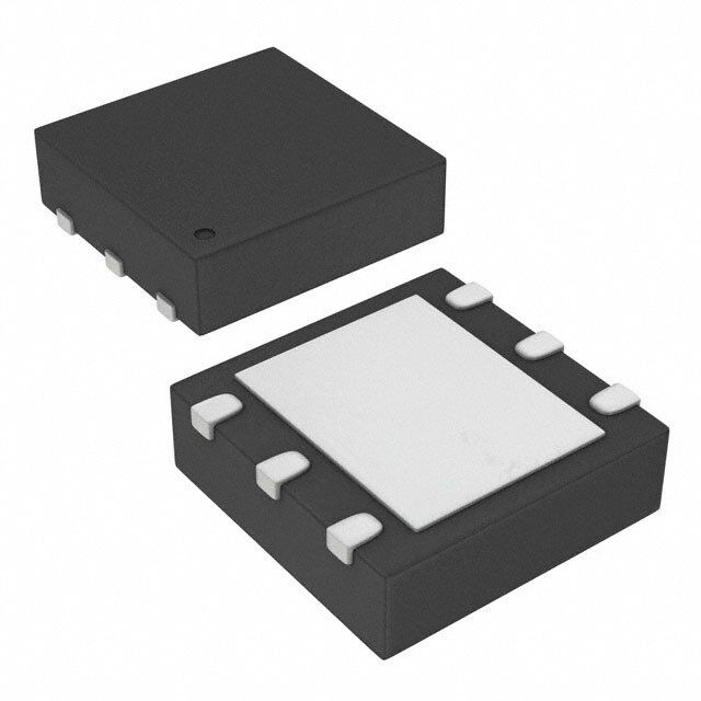
| 供应商器件封装 | 6-VSON 裸露焊盘(3x3) |
| 其它名称 | 296-19361-1 |
| 包装 | 剪切带 (CT) |
| 单位重量 | 25.700 mg |
| 同步整流器 | 无 |
| 商标 | Texas Instruments |
| 安装类型 | 表面贴装 |
| 安装风格 | SMD/SMT |
| 封装 | Reel |
| 封装/外壳 | 6-VDFN 裸露焊盘 |
| 封装/箱体 | VSON-6 |
| 工作温度 | -40°C ~ 125°C |
| 工作温度范围 | - 40 C to + 125 C |
| 工厂包装数量 | 250 |
| 开关频率 | 1.25 MHz |
| 拓扑结构 | Buck |
| 最大工作温度 | + 125 C |
| 最大输入电压 | 8 V |
| 最小工作温度 | - 40 C |
| 标准包装 | 1 |
| 电压-输入 | 4.5 V ~ 8 V |
| 电压-输出 | 0.8 V ~ 7 V |
| 电流-输出 | 1.6A |
| 类型 | Step-Down Switching Voltage Regulator |
| 系列 | TPS40222 |
| 输入电压 | 4.5 V to 8 V |
| 输出数 | 1 |
| 输出电压 | 800 mV to 8 V |
| 输出电流 | 1.6 A |
| 输出端数量 | 1 Output |
| 输出类型 | 可调式 |
| 配用 | /product-detail/zh/TPS40222EVM-001/296-21154-ND/1216760 |
| 频率-开关 | 1.25MHz |


- 商务部:美国ITC正式对集成电路等产品启动337调查
- 曝三星4nm工艺存在良率问题 高通将骁龙8 Gen1或转产台积电
- 太阳诱电将投资9.5亿元在常州建新厂生产MLCC 预计2023年完工
- 英特尔发布欧洲新工厂建设计划 深化IDM 2.0 战略
- 台积电先进制程称霸业界 有大客户加持明年业绩稳了
- 达到5530亿美元!SIA预计今年全球半导体销售额将创下新高
- 英特尔拟将自动驾驶子公司Mobileye上市 估值或超500亿美元
- 三星加码芯片和SET,合并消费电子和移动部门,撤换高东真等 CEO
- 三星电子宣布重大人事变动 还合并消费电子和移动部门
- 海关总署:前11个月进口集成电路产品价值2.52万亿元 增长14.8%


PDF Datasheet 数据手册内容提取
TPS40222 www.ti.com SLUS642A–OCTOBER2005–REVISEDJANUARY2006 · 1.6-A, 1.25-MHz BUCK CONVERTER IN A 3 mm 3 mm SON PACKAGE FEATURES APPLICATIONS • InputVoltageRange4.5V to8V • DiskDrives DC DC • OutputVoltage(0.8Vto90%V ) • SetTopBox IN • 0Ato1.6ACurrentCapability • PointofLoadPower • Fixed1.25-MHzSwitchingFrequency • ASICPowerSupplies • Reference0.8V±1% DESCRIPTION • Internal250mW N-ChannelMOSFETSwitch The TPS40222 is a fixed-frequency, current-mode, • CurrentModeControlwithInternalSlope non-synchronous buck converter optimized for Compensation applications powered by a 5-V distributed source. • InternalSoft-Start With internally determined operating frequency, • InternalLoopCompensation soft-start time, and control loop compensation, the TPS40222 provides many features with a minimum of • ShortCircuitProtection externalcomponents. • ThermalShutdown The TPS40222 operates at 1.25 MHz and supports • HighEfficiencyUpto92% up to 1.6-A output loads. The output voltage can be • Small3mm· 3mmSONPackage programmed to as low as 0.8 V. The TPS40222 utilizes pulse-by-pulse current limit as well as frequency foldback to protect the converter during a catastrophicshortcircuitedoutputcondition. SIMPLIFIEDAPPLICATIONDIAGRAM TYPICALEFFICIENCY vs LOADCURRENT 100 VIN VIN = 5 V 95 C1 6 5 4 90 BOOSTAVIN PVIN TPS40222 C2 % 85 VOUT = 3.3 V − y FB GND SW c en 80 1 2 3 VOUT ci L1 Effi − 75 h R1 70 C3 VOUT = 1.25 V D1 65 R2 60 UDG−04135 0 0.2 0.4 0.6 0.8 1.0 1.2 1.4 1.6 ILOAD − Load Current − A Pleasebeawarethatanimportantnoticeconcerningavailability,standardwarranty,anduseincriticalapplicationsofTexas Instrumentssemiconductorproductsanddisclaimerstheretoappearsattheendofthisdatasheet. PRODUCTIONDATAinformationiscurrentasofpublicationdate. Copyright©2005–2006,TexasInstrumentsIncorporated Products conform to specifications per the terms of the Texas Instruments standard warranty. Production processing does not necessarilyincludetestingofallparameters.
TPS40222 www.ti.com SLUS642A–OCTOBER2005–REVISEDJANUARY2006 These devices have limited built-in ESD protection. The leads should be shorted together or the device placedinconductivefoamduringstorageorhandlingtopreventelectrostaticdamagetotheMOSgates. ORDERINGINFORMATION T OUTPUTVOLTAGE PACKAGE PARTNUMBER MEDIUM QTY J TPS40222DRPT Smalltapeandreel 250 -40°Cto125°C Adjustable PlasticSON(DRP) TPS40222DRPR Largetapeandreel 3000 ABSOLUTE MAXIMUM RATINGS overfree-airtemperaturerangeunlessotherwisenoted(1) TPS40222 UNIT BOOST 19 SW(50nsmaximum) –5 V Inputvoltagerange SW –2to16 V IN AVIN,PVIN 10 FB -0.3to2 I Outputcurrentsource SW 3.5 A OUT T Operatingjunctiontemperaturerange –40to160 J T Storagetemperature –65to165 °C stg Casetemperaturefor10secondsperJSTD-020C 260 (1) Stressesbeyondthoselistedunder"absolutemaximumratings"maycausepermanentdamagetothedevice.Thesearestressratings only,andfunctionaloperationofthedeviceattheseoranyotherconditionsbeyondthoseindicatedunder"recommendedoperating conditions"isnotimplied.Exposuretoabsolute-maximum-ratedconditionsforextendedperiodsmayaffectdevicereliability. RECOMMENDED OPERATING CONDITIONS MIN NOM MAX UNIT V Inputvoltage 4.5 8.0 V IN I SWnodeoutputcurrent 0 1.6 A OUT T Operatingjunctiontemperature -40 125 °C J ELECTROSTATIC DISCHARGE (ESD) PROTECTION MIN MAX UNIT Humanbodymodel 2500 V CDM 1500 2
TPS40222 www.ti.com SLUS642A–OCTOBER2005–REVISEDJANUARY2006 ELECTRICAL CHARACTERISTICS T =-40°Cto125°C,4.5£ V =V £ 5.5V(unlessotherwisenoted) J AVIN PVIN PARAMETER TESTCONDITIONS MIN TYP MAX UNIT FEEDBACKVOLTAGE T =25°C,Noload 792 800 808 J VFB Feedbackvoltage -44.50V°C£ £VTJ££ 172V5°C,Noload, 788 812 mV DD I Feedbackinputbiascurrent V =0.9V,V =V =5V 30 100 nA FB FB AVIN PVIN SOFT-START t Soft-starttime V =V =5V 300 550 850 µs SS AVIN PVIN GmAMPLIFIER Gm Transconductance(1) 10 µS GBW Gainbandwidthproduct(1) 12 MHz OSCILLATOR f Switchingfrequency V >0.7V 1.00 1.25 1.50 MHz SW FB f Minimumfoldbackfrequency Startup/Overcurrent,V =0V 75 140 kHz SWFB FB Foldbackfrequencyslope(1) 0V<V <0.4V 2200 Hz/mV FB V FrequencyfoldbackV thresholdvoltage(1) 0.4 0.6 V FFB FB OVERCURRENTDETECTION I Overcurrentthreshold V =V =5V 2.1 2.6 3.1 A CL AVIN PVIN t Minimumon-timeinovercurrent(1) 90 200 ns ON HIGHSIDEMOSFETANDDRIVER T =25°C 250 R Drain-to-sourceon-resistance J mW DS(on) -40°C£ T£ 125°C 250 550 J D Maximumdutycycle 90% 97% MAX I MOSFETSWleakagecurrent V =10V -10 -30 µA SWL PVIN I Boostcurrent I =100mA,V =V =5V 0.5 1.0 mA BOOST SW AVIN PVIN Boostdiodevoltagedrop I £ 5mA 0.9 V DIODE UNDERVOLTAGELOCKOUT(UVLO) V Turn-onvoltage 3.6 3.8 4.0 ON V V Hysteresisvoltage 0.4 HYST I AVINquiescentcurrent 1.0 1.5 mA Q THERMALSHUTDOWN Thermalshutdownvoltage(1) 150 °C Thermalhysteresis(1) -10 (1) Ensuredbydesign.Notproductiontested. 3
TPS40222 www.ti.com SLUS642A–OCTOBER2005–REVISEDJANUARY2006 DRP PACKAGE (BOTTOM VIEW) BOOST 6 1 FB AVIN 5 2 GND PVIN 4 3 SW A. Exposedpadprovidesalowthermalresistanceofq =2(cid:176) C/W JC B. ConnectexposedpadtoGND. Table1.TERMINALFUNCTIONS TERMINAL I/O DESCRIPTION NAME NO. Inputpowertothecontrolsectionofthedevice.CloselybypassthispintoGNDwithalowESRceramiccapacitor AVIN 5 I of1-µForgreater. Thispinprovidesabootstrappedsupplyforthehigh-sideMOSFETdriverforPWM,enablingthegateofthe BOOST 6 I/O high-sideMOSFETtobedrivenabovetheinputsupplyrail.Connecta33-nFcapacitorfromthispintoSWpinand (optionally)aSchottkydiodefromthispintothePVINpin. Invertinginputoftheerroramplifier.Inclosed-loopoperation,thevoltageatthispinistheinternalreferencelevel of800mV.Duringstartuporfaultconditions,thevoltageonthispinalsoaffectstheoperatingfrequencyofthe FB 1 I converter.With0Vonthepin,theoperatingfrequencyisapproximately140kHz.Thefrequencyincreaseslinearly toapproximately1.25MHzasthevoltageonthepinisraisedto0.6V.Above0.6V,theoperatingfrequency remainsatapproximately1.25MHz. GND 2 - Groundconnectiontothedevice. PVIN 4 I Inputtothepowersectionofthedevice.BypassthispintoGNDwithalowESRcapacitorof10-µForgreater. ThesourceconnectionoftheinternalswitchingMOSFET.Connectthispintotheoutputinductorandanexternal SW 3 I/O catchdiodetoformtheconverter'sswitchnode. 4
TPS40222 www.ti.com SLUS642A–OCTOBER2005–REVISEDJANUARY2006 SIMPLIFIEDBLOCKDIAGRAM BOOST PVIN 6 4 TPS40222 0.5 VREF Oscillator f(VOSC) BDiCas f(IDRAIN) DBiooodset IDRAIN FB TSD Composite Ramp PWM Soft Start E/A + Comparator 0.8 VREF + FB 1 S Q 2 MW Thermal R Q 3 SW Shutdown 16 pF f(IDRAIN) + Overcurrent 0.8 VREF Comparator AVIN 5 References 0.5 VREF Current Limit Threshold 2 GND UDG−04129 5
TPS40222 www.ti.com SLUS642A–OCTOBER2005–REVISEDJANUARY2006 TYPICAL CHARACTERISTICS FEEDBACKVOLTAGE FEEDBACKVOLTAGE vs vs INPUTVOLTAGE(NOLOAD) JUNCTIONTEMPERATURE 803 803 802 802 e − mV 801 ge − V 801 g a olta Volt k V ck c 800 a 800 a b b d d e e e e F − FB 799 − FB 799 F V V 798 798 797 797 4 5 6 7 8 9 −50 −25 0 25 50 75 100 125 VIN − Input Voltage − V TJ − Junction Temperature − °C Figure1. Figure2. OSCILLATORFREQUENCY OSCILLATORFREQUENCY vs vs FEEDBACKVOLTAGE INPUTVOLTAGE 1.3 1.30 VFB = 0.8 V VIN = 5 V 1.1 1.28 z MH 0.9 Hz M cy − y − 1.26 n c e 0.7 n u e q u e q f − Fr 0.5 f − Fre 1.24 1.22 0.3 0.1 1.20 0 0.1 0.2 0.3 0.4 0.5 0.6 0.7 0.8 4 5 6 7 8 9 VFB − Feedback Voltage − V VIN − Input Voltage − V Figure3. Figure4. 6
TPS40222 www.ti.com SLUS642A–OCTOBER2005–REVISEDJANUARY2006 TYPICAL CHARACTERISTICS (continued) OVERCURRENT OVERCURRENT vs vs INPUTVOLTAGE JUNCTIONTEMPERATURE(V =5V) IN 2.9 2.9 2.8 2.8 A A I − Overcurrent − CL 22..76 I − Overcurrent − CL 22..76 2.5 2.5 2.4 2.4 4.5 5.0 5.5 6.0 6.5 7.0 −50 −25 0 25 50 75 100 125 VIN − Input Voltage − V TJ − Junction Temperature − °C Figure5. Figure6. SWITCHINGMOSFETON-RESISTANCE SOFT-STARTTIME vs vs JUNCTIONTEMPERATURE JUNCTIONTEMPERATURE 0.35 700 650 W− 0.30 s n−Resistance 0.25 mStart TIme − 565000 Maximum O − − oft S(on) − SS 500 D S R 0.20 T 450 Minimum 0.15 400 −50 −25 0 25 50 75 100 125 −50 −25 0 25 50 75 100 125 TJ − Junction Temperature − °C TJ − Junction Temperature − °C Figure7. Figure8. 7
TPS40222 www.ti.com SLUS642A–OCTOBER2005–REVISEDJANUARY2006 DETAILED DESCRIPTION The TPS40222 is a fixed frequency PWM controller incorporating an internal high-side MOSFET switch and is intendedfornon-synchronousconverterapplicationsrequiringloadcurrentofupto1.6A. Feedback Control To maintain output voltage regulation, a fixed-frequency, current-mode-control architecture is employed. A transconductance error amplifier with internal compensation senses the output voltage through a resistive divider andcomparestheresultwith an internal 0.8-V precision reference voltage. The result of this comparison is fed to the inverting input of a PWM comparator. A composite sawtooth voltage waveform is fed in to the non-inverting inputresultingataPWMsignalatthecomparatoroutput. To generate the sawtooth ramp signal, the load current is sensed through the high-side MOSFET during the ON portion of the switching cycle. The sensed current is then split and fed into two trimmed resistor banks that are used to generate the ramps for the PWM control and the pulse-by-pulse current limit. This method of sensing does not require a sense resistor in the high-current path. The portion of the load current for PWM control is then summed with a signal proportional to the oscillator sawtooth, plus a small portion of DC bias to create the compositerampsignal. UVLO An internal circuit will turn on the converter when the AVIN voltage rises above approximately 3.8 V. At voltages belowthislevel,theinternaloscillatorisdisabledandtheinternalMOSFETisbiasedoff. Reference Theprecisionbandgapreferenceof0.8Vistrimmedto1%. Voltage Error Amplifier The internal transconductance amplifier is used to control the output voltage. A series R-C circuit (2 MW , 16 pF) fromtheoutputoftheamplifiertogroundservesasthecompensationcircuitfortheconverter. Oscillator During normal operation, the internal oscillator runs at a nominal 1.25 MHz. During startup, the oscillator starts at a slower frequency, then as the output voltage rises, the frequency is increased to the nominal operating frequency. The switch-over point occurs when the FB pin voltage exceeds 0.6 V. Above 0.6 V, the oscillator remainsatanominal1.25MHz. AsignalderivedfromtheoscillatorrampisusedtodevelopslopecompensationforPWMcontrol. 8
TPS40222 www.ti.com SLUS642A–OCTOBER2005–REVISEDJANUARY2006 DETAILED DESCRIPTION (continued) Soft-Start During power-on, the TPS40222 slowly increases the voltage to the non-inverting input to the error amplifier. In this way, the TPS40222 slowly ramps up the output voltage until the voltage on the non-inverting input to the error amplifier reaches 0.8 V. At that time, the voltage at the non-inverting input to the error amplifier remains at 0.8V. Upon startup, the time for the voltage on the non-inverting input of the error amplifier to reach 0.8 V is approximately 550 µs. The rate of rise of the voltage on the output of a TPS40222 is determined by the resistive dividernetworkthatsetstheconverteroutputvoltage. Forexample,therateofriseoftheinternalsoft-startis: V REF(cid:1) 0.8V t 550(cid:1)s SS (1) where • t intheexampleisthetypicalsoft-starttimeof550µs SS Fora1.2-Voutputconverter,therateofriseobservedattheoutputis: V OUT(cid:1) 1.2V t 550(cid:1)s SS (2) Output Short-Circuit Protection Currentfault(short-circuit)protectionisprovidedbysensingthecurrentthroughtheswitchingMOSFET while it is in the ON state and comparing with a preset internal level. If the current exceeds this level, the switching pulse width is limited causing the output voltage to decay. As the output voltage decays, the operating frequency is alsodecreased,therebyreducingpowerdissipation. If the fault condition persists, and the output voltage continues to decay, then a watchdog circuit discharges the internal soft-start capacitor, effectively shutting off the converter. When this interval is completed, the converter thenattemptstorestart. Bootstrap To drive the internal N-channel MOSFET, a bootstrap, or boost circuit, is added to provide a voltage source higher than the input voltage of sufficient energy to fully enhance the MOSFET each switching cycle. During the freewheeling portion of the switching cycle (refer to Figure 9), the internal MOSFET is off, and the voltage at the SW node is clamped to just below ground by D1. At this time the input voltage (less the drop of the internal BOOST diode) is impressed upon C2, allowing it to charge. When the internal MOSFET is commanded to turn ON, the SW node rises towards V , and the voltage on the BOOST pin rises to approximately 2 × V . This IN IN voltageisusedtofurtherturnontheinternalMOSFETfortheremainderoftheswitchingcycle. 9
TPS40222 www.ti.com SLUS642A–OCTOBER2005–REVISEDJANUARY2006 APPLICATION INFORMATION Typical Application VIN C1 6 5 4 BOOST AVIN PVIN TPS40222 C2 FB GND SW 1 2 3 L1 VOUT R1 D1 C3 R2 UDG−04131 Figure9.TypicalApplication Voltage Setting Theoutputvoltagemaybesetbyknowingthatthefeedbackvoltageis0.8Vandusing Equation 3. To determine anoutputvoltage,chooseaconvenientresistorvalueforR2andcalculateR1. (cid:4) R1(cid:5) VOUT(cid:3)VFB(cid:1) 1(cid:2)R2 (3) Output Filter (L1 and C3) Since the loop compensation is internally fixed and cannot be changed, loop stability can only be controlled by the proper choice of output inductance and capacitance. Table 2 provides a shortcut guide to this selection and recommended capacitance to maintain a safe 50 degrees of phase margin for various inductors and output voltages. The table also shows the minimum capacitance for 50 degress of phase margin at three temperatures, with the worst case for stability at -40(cid:176) C. The granularity of the table is sufficient so the user can interpolate betweenvaluestofindaspecificoperatingcondition.Thetablevaluesassumea full load, which is also the worst case for phase compensation. As an example of using the table, consider a 2.5-V output converter with a 2.2-m H inductor. The table shows that a minimum of 15-m F of output capacitance is required to guarantee greater than 50 degress of phase margin at the worst case temperature of -40(cid:176) C. With a lead capacitor (C ) added to the LEAD feedback as shown in Figure 10, this minimum capacitance increases to 26-m F and the closed-loop frequency increasesbyabout20%. 10
TPS40222 www.ti.com SLUS642A–OCTOBER2005–REVISEDJANUARY2006 APPLICATION INFORMATION (continued) Table2.CapacitorSelection(1) INDUCTOR C (m F) VA(mLHU)E C5U-RVRINERNIPTP(mLEA) (PM-M4I>N0(cid:176)5C0)(cid:176) at TfJC=(k-4H0z(cid:176))C TfJC=(k2H5z(cid:176))C TJfC=(k1H25z)(cid:176) C VALCULEEAD(pF) OUTPUTVOLTAGEV =3.3V OUT 1.8 NotRecommended(2) 9 125 101 68 omitted 2.2 340 21 285 247 92 270 12 98 77 52 omitted 3.3 230 28 144 112 67 330 15 80 62 41 omitted 4.7 160 38 111 85 52 470 16 74 58 38 omitted 5.6 140 40 103 79 47 470 OUTPUTVOLTAGEV =2.5V OUT 13 116 93 63 omitted 1.8 550 23 169 133 81 330 15 102 81 54 omitted 2.2 370 26 147 114 65 330 17 91 71 48 omitted 3.3 300 28 134 102 56 270 20 78 61 41 omitted 4.7 210 38 106 81 47 470 23 68 53 35 omitted 5.6 180 34 106 79 43 330 OUTPUTVOLTAGEV =1.8V OUT 20 105 84 56 omitted 1.8 580 30 137 109 68 470 21 100 80 54 omitted 2.2 470 32 129 101 62 470 25 86 67 45 omitted 3.3 320 35 115 88 53 470 30 72 56 37 omitted 4.7 220 39 99 75 44 470 33 65 51 34 omitted 5.6 190 40 94 71 41 470 OUTPUTVOLTAGEV =0.8V OUT 1.8 470 50 94 75 50 2.2 390 52 91 72 48 3.3 260 60 79 62 42 n/a 4.7 180 70 68 53 36 5.6 150 75 63 49 33 (1) SeeFigure10. (2) ForV >3.3Vuseaninductorwithavaluegreaterthanorequalto2.2m H. OUT 11
TPS40222 www.ti.com SLUS642A–OCTOBER2005–REVISEDJANUARY2006 Output Stage Component Selection In most applications, the user starts with a known output voltage and current load requirement as shown in Figure10. L1 VOUT 2.2 m H 3.3 V PVIN TPS40222 SW 1.5 A 4 3 AVIN GND 5 2 R1 BOOST FB 31.25 kW CLEAD C0 6 1 + R2 Internal 10 kW VREF 800 mV UDG−05095 Figure10.OutputStage As shown in Figure 10, the trimmed reference voltage is internally connected to the error amplifier. Since the input bias current to this error amplifier is negligible. The feedback resistors R1 and R2 can be selected over a broad range limited by the low bias current into the error amplifier. With this restriction in mind, R2 was selected at 10 kW , so its current is 80 m A and large relative to the bias current of the error amplifier. The output voltage is thengivenbyEquation4. (cid:4) R1(cid:5) VOUT(cid:3)0.8(cid:1) 1(cid:2)R2 (cid:3)3.3V (4) where • R1=31.25kW • R2=10kW Inductor Selection This device's high-frequency internal clock enables the use of smaller, less expensive inductors. Ferrite, with its good high frequency properties, is the material of choice. Several manufacturers provide catalogs with inductor saturation currents, inductance values, and LSRs (internal resistance) for their various sized ferrites. For a 3.3-V, 1.5 A application, the inductor's saturation current must be higher than the maximum output current plus ½ the ripple current. The inductor value sets the ripple current. A small inductor provides better transient response and is a smaller, less expensive part. Too low an inductor value, however, causes high ripple currents that cause high ripple voltage across the ESR of the output capacitance. A rule of thumb is to set high ripple current to be lessthan30%oftheoutputcurrent.Afirstordercalculationthengives: (cid:1)V(cid:1)t L(cid:2) ON (cid:1)I (5) where • D Vistheinputvoltage-(IRdropsintheinductorandFET)-V OUT • D Iis30%of1.5A • t istheontimegivenby(V /(V · f))wheref=1.25MHz ON OUT IN Undertheseconditions,L=1.55m H Selecting a standard value 2.2-m H inductor, with an internal resistance of 32 mW , the peak current developed duringtheontimeis1.66A.Thisvalueissafelybelowthedevice'sbuiltinovercurrentlimitof2.1A. 12
TPS40222 www.ti.com SLUS642A–OCTOBER2005–REVISEDJANUARY2006 Capacitor Selection One constraint on the capacitance is the overshoot allowed by a sudden load change. The worst case for a transient load release occurs at the time when the inductor has just finished a t pulse. At this point, the ON inductor is operating at maximum current. When the output load is suddenly removed, all of the inductor current mustbeabsorbedbytheoutputcapacitance. With a typical output voltage overshoot requirement of 2% at 3.3-V, theminimumcapacitancerequiredtoremaininspecificationiscalculatedusingEquation6. 12(cid:1)LO(cid:1)(cid:4)IO(cid:5)2(cid:3)12 CO(cid:4)VOS2(cid:2)VO2(cid:5) (6) where • V isthemaximumovershootvoltage OS • L =2.2m H O • I =1.5A O • V =3.3V O Solvingthisrelationship,theminimumrequiredoutputcapacitanceC is11-m F. O The other load transition extreme is from no load to full load that occurs just after a minimum on-time cycle has started. At this point, the controller has to support this load for the remainder of the cycle with a minimum of current available from the inductor. In this example, the minimum on-time with a 3.3-V output is 528 ns and the off-timeis800nsminus528ns=272ns.UsingtherelationshipshowninEquation7; I (cid:1)(cid:1)t C (cid:2) O (cid:2)6.1(cid:2)F MIN (cid:1)V OUT (7) where • D V isa2%specifiedoutputvoltagedroop OUT • I =1.5A O • D t=272ns Ceramic capacitors with a low ESR are used to achieve the lowest voltage ripple. For example, current 1206, 6.3-Vcapacitorsthatprovide22m FandanESRof2mW areavailable. 13
TPS40222 www.ti.com SLUS642A–OCTOBER2005–REVISEDJANUARY2006 These component selection decisions influence the phase margin and hence the stability of the system. For example, raising the output capacitance reduces the system crossover frequency and raises phase margin. Figure 11 illustrates this in a curve that shows phase margin as a function of output capacitance for two widely different inductors. The curves show that beyond a certain point, added capacitance has limited benefit. This point can be exploited to avoid the expense of excessive output capacitance. The curves also show the advantage of a lower inductance, where only 20-m F of output capacitance is required to obtain 60 degrees of phasemargin. The output voltage affects the phase margin by changing the equivalent output resistance to deliver full load. With a higher output voltage for example, there is a higher full-load resistance and a lower output capacitance is required for the same phase margin. An idea of this effect is illustrated in Figure 12 which plots the required minimum capacitance to achieve 50 degrees of phase margin at different output voltages. The curves also show thereductioninoutputcapacitancethatmaybeachievedwithalowerinductorvalue. PHASEMARGIN OUTPUTVOLTAGE vs vs OUTPUTCAPACITANCE OUTPUTCAPACITANCE 100 6 L = 1.8 m H PHASE = 50° 90 5 70 V − °n − 60 L = 5.6 m H oltage 4 argi 50 ut V 3 L = 5.6 m H M p se 40 Out Pha 30 − UT 2 O V 20 1 L = 2.2 m H 10 VOUT = 1.8 V 0 0 0 20 40 60 80 100 120 0 10 20 30 40 50 60 70 80 COUT − Output Capacitance − m F COUT − Output Capacitance − m F Figure11. Figure12. A further improvement in reducing output capacitance is made by adding a lead capacitor across R1 of the feedback network. This lead capacitor can be determined by making its impedance equal to the resistance of R1 attheresonantfrequencyoftheoutputL-Cnetwork.TheleadcapacitanceiscalculatedusingEquation8. C (cid:2) 1 LEAD 2(cid:1)(cid:1)f (cid:1)R R (8) TheresonantfrequencyformedbytheinductorandtheoutputloadcapacitanceiscalculatedinEquation9. 1 1 (cid:3) 1 (cid:4)2 fR(cid:2)2(cid:1)(cid:1) L(cid:1)CO (9) Catch Diode (D1) The selection of the catch diode depends on the application current. Select a diode that has a low forward voltagedrop,andalowjunctioncapacitance.Adiode with too high of a forward voltage drop or a diode with high junction capacitance result in a converter that has poor efficiency, as well as excessive ringing on the SW node andexcessiveoutputvoltagenoise. 14
TPS40222 www.ti.com SLUS642A–OCTOBER2005–REVISEDJANUARY2006 Input Filter Capacitor (C1) Select a good quality, low ESR ceramic capacitor to bypass the input. For a conservative design, the capacitor shouldhavearipplecurrentratingequaltotheloadcurrentoftheconverter. Boost Capacitor (C2) The boost capacitor is sized to ensure there is enough energy available to turn on the internal MOSFET. For mostapplications,useaceramiccapacitorwithavaluebetween33nFand100nF. D2 VIN C1 6 5 4 BOOST AVIN PVIN TPS40222 C2 FB GND SW 1 2 3 L1 VOUT R1 D1 C3 R2 UDG−04132 Figure13.UsingaBoostDiode Boost Diode (D2) For some applications, the internal bootstrap diode’s voltage drop may be too high to sufficiently charge the boost capacitor each switching cycle. For these applications, a Schottky diode, D2 shown in Figure 13, may be added. Output Preload Requirement One of the requirements for proper startup of the DC-to-DC converter is that the boost capacitor, C2, has sufficient voltage across it before switching occurs. In some applications, notably those with output voltages of 3.3 V, and those with slowly rising or low input voltages, there is the need to add a small 10 mA, pre-load to the converter to hold the SW node to GND before switching begins. Without a pre-load, the output voltage may not reach regulation. In addition, the pre-load prevents the output from overshooting too much when the load is steppedfromahighvaluetozero. AVIN Filtering Some applications may require the addition of an R-C filter on the input of AVIN to filter unwanted noise and improve load regulation. (See Figure 14) Use R4=10 W and C5=1 µF. Connect the ground side of C5 as close as possibletotheGNDpinofthedevice. SW Node Snubber ToattenuateexcessiveringingattheSWnode,anR-CnetworkmaybeaddedacrossD1.(SeeFigure14) Use R3=10 W and C4=680 pF as a starting point. Decrease C4 until the minimum capacitance is found for the desiredringingattenuation. 15
TPS40222 www.ti.com SLUS642A–OCTOBER2005–REVISEDJANUARY2006 VIN R4 C1 C5 6 5 4 BOOST AVIN PVIN TPS40222 C2 FB GND SW 1 2 3 L1 VOUT R3 C3 R1 C4 D1 R2 UDG−04130 Figure14.AVINFilterandSWNodeSnubber 16
TPS40222 www.ti.com SLUS642A–OCTOBER2005–REVISEDJANUARY2006 Application Circuit Schematic Figure 15 shows an example of an application incorporating a TPS40222 in a 1.2-V output DC-to-DC converter. NoticetheuseofparallelcapacitorsattheinputandtheoutputtoreducetheeffectiveESRofthecapacitance. +VIN 4.5 V to 5.5 V TP1 1 C1A C1B C1C 22 m F 22 m F 0.1 m F J1 R4 2 GND TP2 C5 1 m F 6 5 4 BOOST AVIN PVIN TPS40222 C2 FB GND SW 33 nF 1 2 3 TP3 L1 3.3 m H 1 2 R3 D1 C223 Am F C223 Bm F +1.V2O VUT 1 C4 R1 5.6 kW R5 J2 2 GND R2 10 kW TP4UDG−05099 Figure15.5-V ,1.2V DC-to-DCConverter IN OUT 17
TPS40222 www.ti.com SLUS642A–OCTOBER2005–REVISEDJANUARY2006 Table3.ListofMaterials REFERENCE VENDORPART QTY DESCRIPTION VENDOR NOTES DESIGNATOR NUMBER C1A,C1B 2 Capacitor,22µFceramic,1206 Inputbypass High-frequencybypass,mount C1D 1 Capacitor,0.1µFceramic,0805 nearV CC C2 1 Capacitor,33nFceramic,0805 Bootstrap C3A,C3B 2 Capacitor,22µFceramic,1206 Outputcapacitors Snubber(optional-openifnot C4 1 Capacitor,680pFceramic,0805 used) Deviceinputvoltagefilter C5 1 Capacitor,1µFceramic,0805 capacitor D1 1 Diode,Schottky,1A RSX501L-20 ROHM Catchdiode L1 1 Inductor,3.3µH ELL6PV3R3N Panasonic Filterinductor R1 1 Resistor,5620W ,1%,SMD,0603 Voltagesettingresistor R2 1 Resistor,10kW ,1%,SMD,0603 Voltagesettingresistor R3 1 Resistor,10W ,10%,SMD,0805 Snubber(optional-openifnot used) R4 1 Resistor,10W ,10%,SMD,0603 Deviceinputvoltagefilter(optional -shortifnotused) R5 1 Resistor,120W ,10%,SMD,0805 Outputpre-load(optional-openif notused) Texas U1 1 PWMconverterdevice TPS40222 Instruments APPLICATION CURVES OUTPUTVOLTAGE EFFICIENCY vs vs INPUTVOLTAGEATLOADCURRENT LOADCURRENT 1.410 100 IOUT = 1.0 A VIN = 5 V 95 1.408 90 V IOUT = 1.5 A − e Output Voltag11..440064 IOUT = 0.5 A Efficiency − % 8805 VOUT = 3.3 V − T − 75 OU h V 70 VOUT = 1.25 V 1.402 No Load 65 1.400 60 4.0 4.5 5.0 5.5 6.0 6.5 7.0 0 0.2 0.4 0.6 0.8 1.0 1.2 1.4 1.6 VIN − Input Voltage − V ILOAD − Load Current − A Figure16. Figure17. 18
TPS40222 www.ti.com SLUS642A–OCTOBER2005–REVISEDJANUARY2006 TYPICAL CHARACTERISTICS SW 2 V/ div VOUT (0.5 V/ div) VIN (1 V/ div) t − Time − 200 m s/div t − Time − 100 ns/div Figure18.StartupWaveform Figure19.SWNodeWaveform GAINANDPHASE vs FREQUENCY 50 180 40 135 PHASE 30 90 20 45 − dB 10 0 °e − ain GAIN has G P 0 −45 −10 −90 −20 −135 −30 −180 100 1 k 10 k 100 k 1 M f − Frequency − Hz Figure20. 19
TPS40222 www.ti.com SLUS642A–OCTOBER2005–REVISEDJANUARY2006 PC BOARD LAYOUT RECOMMENDATIONS Device Pad Design The 6-pin package has an exposed thermal pad intended to help conduct heat out of the package, allowing a higher than otherwise available operating ambient temperature. Place three vias within the pad area, tying them toananaloggroundplane. PCB Layout WhendesigningaDC-to-DCconverterlayout,caremustbetakentoensureanoise-freedesign. VIN C1 6 5 4 BOOST AVIN PVIN TPS40222 C2 FB GND SW 1 2 3 L1 VOUT B D1 C3 R1 A R2 UDG−04134 Figure21.EnsuringaNoise-FreeLayout • AC current loops must be kept as short as possible. The input loop B (C1-U1-D1) in the figure must be kept short to ensure proper filtering by C1 for the device. Excessive high frequency noise on AVIN during switching could degrade overall regulation as the load increases. In order to reduce noise spikes seen by the device, an R-C filter is recommended (see AVIN Filtering in the APPLICATION INFORMATION section) and asnubbermaybeadded(seeSWNodeSnubberintheAPPLICATIONINFORMATIONsection). • The output loop A (D1-L1-C3) should also be kept as small as possible. Noise performance at the output of theconvertersuffersiftheloopareaistoolarge. • It is recommended that traces carrying large AC currents NOT be connected through a ground plane. Instead, use PCB traces on the top layer to conduct the AC current and use the ground plane as a noise shield. Split the ground plane as necessary to keep noise away from the TPS40222 and noise sensitive areas(R1,R2). • Keep the SW node as physically small as possible to minimize parasitic capacitance and to minimize radiatedemissions • For good output voltage regulation, R1 should be connected close to the load. The R2-TPS40222 (GND) connectionshouldbetiedclosetotheloadaswell. • ThetracefromtheR1-R2 junction to the TPS40222 should be kept away from any noise source, such as the SWnode,ortheboostcircuitry. • The GND pin and the thermal pad of the TPS40222 should be connected together under the device as indicated in the pad design section. For good thermal conductivity, VIAs directly under the device should connectthethermalpadtoagroundplaneontheothersideoftheboard. 20
PACKAGE OPTION ADDENDUM www.ti.com 15-Apr-2017 PACKAGING INFORMATION Orderable Device Status Package Type Package Pins Package Eco Plan Lead/Ball Finish MSL Peak Temp Op Temp (°C) Device Marking Samples (1) Drawing Qty (2) (6) (3) (4/5) TPS40222DRPR ACTIVE VSON DRP 6 3000 Green (RoHS CU NIPDAU Level-2-260C-1 YEAR -40 to 125 0222 & no Sb/Br) TPS40222DRPRG4 ACTIVE VSON DRP 6 3000 Green (RoHS CU NIPDAU Level-2-260C-1 YEAR -40 to 125 0222 & no Sb/Br) TPS40222DRPT ACTIVE VSON DRP 6 250 Green (RoHS CU NIPDAU Level-2-260C-1 YEAR -40 to 125 0222 & no Sb/Br) (1) The marketing status values are defined as follows: ACTIVE: Product device recommended for new designs. LIFEBUY: TI has announced that the device will be discontinued, and a lifetime-buy period is in effect. NRND: Not recommended for new designs. Device is in production to support existing customers, but TI does not recommend using this part in a new design. PREVIEW: Device has been announced but is not in production. Samples may or may not be available. OBSOLETE: TI has discontinued the production of the device. (2) Eco Plan - The planned eco-friendly classification: Pb-Free (RoHS), Pb-Free (RoHS Exempt), or Green (RoHS & no Sb/Br) - please check http://www.ti.com/productcontent for the latest availability information and additional product content details. TBD: The Pb-Free/Green conversion plan has not been defined. Pb-Free (RoHS): TI's terms "Lead-Free" or "Pb-Free" mean semiconductor products that are compatible with the current RoHS requirements for all 6 substances, including the requirement that lead not exceed 0.1% by weight in homogeneous materials. Where designed to be soldered at high temperatures, TI Pb-Free products are suitable for use in specified lead-free processes. Pb-Free (RoHS Exempt): This component has a RoHS exemption for either 1) lead-based flip-chip solder bumps used between the die and package, or 2) lead-based die adhesive used between the die and leadframe. The component is otherwise considered Pb-Free (RoHS compatible) as defined above. Green (RoHS & no Sb/Br): TI defines "Green" to mean Pb-Free (RoHS compatible), and free of Bromine (Br) and Antimony (Sb) based flame retardants (Br or Sb do not exceed 0.1% by weight in homogeneous material) (3) MSL, Peak Temp. - The Moisture Sensitivity Level rating according to the JEDEC industry standard classifications, and peak solder temperature. (4) There may be additional marking, which relates to the logo, the lot trace code information, or the environmental category on the device. (5) Multiple Device Markings will be inside parentheses. Only one Device Marking contained in parentheses and separated by a "~" will appear on a device. If a line is indented then it is a continuation of the previous line and the two combined represent the entire Device Marking for that device. (6) Lead/Ball Finish - Orderable Devices may have multiple material finish options. Finish options are separated by a vertical ruled line. Lead/Ball Finish values may wrap to two lines if the finish value exceeds the maximum column width. Important Information and Disclaimer:The information provided on this page represents TI's knowledge and belief as of the date that it is provided. TI bases its knowledge and belief on information provided by third parties, and makes no representation or warranty as to the accuracy of such information. Efforts are underway to better integrate information from third parties. TI has taken and Addendum-Page 1
PACKAGE OPTION ADDENDUM www.ti.com 15-Apr-2017 continues to take reasonable steps to provide representative and accurate information but may not have conducted destructive testing or chemical analysis on incoming materials and chemicals. TI and TI suppliers consider certain information to be proprietary, and thus CAS numbers and other limited information may not be available for release. In no event shall TI's liability arising out of such information exceed the total purchase price of the TI part(s) at issue in this document sold by TI to Customer on an annual basis. Addendum-Page 2
PACKAGE MATERIALS INFORMATION www.ti.com 30-May-2019 TAPE AND REEL INFORMATION *Alldimensionsarenominal Device Package Package Pins SPQ Reel Reel A0 B0 K0 P1 W Pin1 Type Drawing Diameter Width (mm) (mm) (mm) (mm) (mm) Quadrant (mm) W1(mm) TPS40222DRPR VSON DRP 6 3000 330.0 12.4 3.3 3.3 1.1 8.0 12.0 Q2 TPS40222DRPT VSON DRP 6 250 180.0 12.4 3.3 3.3 1.1 8.0 12.0 Q2 PackMaterials-Page1
PACKAGE MATERIALS INFORMATION www.ti.com 30-May-2019 *Alldimensionsarenominal Device PackageType PackageDrawing Pins SPQ Length(mm) Width(mm) Height(mm) TPS40222DRPR VSON DRP 6 3000 367.0 367.0 35.0 TPS40222DRPT VSON DRP 6 250 210.0 185.0 35.0 PackMaterials-Page2
None
None
None
IMPORTANTNOTICEANDDISCLAIMER TIPROVIDESTECHNICALANDRELIABILITYDATA(INCLUDINGDATASHEETS),DESIGNRESOURCES(INCLUDINGREFERENCE DESIGNS),APPLICATIONOROTHERDESIGNADVICE,WEBTOOLS,SAFETYINFORMATION,ANDOTHERRESOURCES“ASIS” ANDWITHALLFAULTS,ANDDISCLAIMSALLWARRANTIES,EXPRESSANDIMPLIED,INCLUDINGWITHOUTLIMITATIONANY IMPLIEDWARRANTIESOFMERCHANTABILITY,FITNESSFORAPARTICULARPURPOSEORNON-INFRINGEMENTOFTHIRD PARTYINTELLECTUALPROPERTYRIGHTS. TheseresourcesareintendedforskilleddevelopersdesigningwithTIproducts.Youaresolelyresponsiblefor(1)selectingtheappropriate TIproductsforyourapplication,(2)designing,validatingandtestingyourapplication,and(3)ensuringyourapplicationmeetsapplicable standards,andanyothersafety,security,orotherrequirements.Theseresourcesaresubjecttochangewithoutnotice.TIgrantsyou permissiontousetheseresourcesonlyfordevelopmentofanapplicationthatusestheTIproductsdescribedintheresource.Other reproductionanddisplayoftheseresourcesisprohibited.NolicenseisgrantedtoanyotherTIintellectualpropertyrightortoanythird partyintellectualpropertyright.TIdisclaimsresponsibilityfor,andyouwillfullyindemnifyTIanditsrepresentativesagainst,anyclaims, damages,costs,losses,andliabilitiesarisingoutofyouruseoftheseresources. TI’sproductsareprovidedsubjecttoTI’sTermsofSale(www.ti.com/legal/termsofsale.html)orotherapplicabletermsavailableeitheron ti.comorprovidedinconjunctionwithsuchTIproducts.TI’sprovisionoftheseresourcesdoesnotexpandorotherwisealterTI’sapplicable warrantiesorwarrantydisclaimersforTIproducts. MailingAddress:TexasInstruments,PostOfficeBox655303,Dallas,Texas75265 Copyright©2019,TexasInstrumentsIncorporated