ICGOO在线商城 > 集成电路(IC) > PMIC - 稳压器 - DC DC 开关稳压器 > TPS62260DRVT

 Datasheet下载
- 型号: TPS62260DRVT
- 制造商: Texas Instruments
- 库位|库存: xxxx|xxxx
- 要求:
| 数量阶梯 | 香港交货 | 国内含税 |
| +xxxx | $xxxx | ¥xxxx |
查看当月历史价格
查看今年历史价格
TPS62260DRVT产品简介:
ICGOO电子元器件商城为您提供TPS62260DRVT由Texas Instruments设计生产,在icgoo商城现货销售,并且可以通过原厂、代理商等渠道进行代购。 TPS62260DRVT价格参考¥4.39-¥9.89。Texas InstrumentsTPS62260DRVT封装/规格:PMIC - 稳压器 - DC DC 开关稳压器, 可调式 降压 开关稳压器 IC 正 0.6V 1 输出 600mA 6-WDFN 裸露焊盘。您可以下载TPS62260DRVT参考资料、Datasheet数据手册功能说明书,资料中有TPS62260DRVT 详细功能的应用电路图电压和使用方法及教程。
TPS62260DRVT 是由 Texas Instruments(德州仪器)生产的一款高效同步降压转换器,属于 PMIC - 稳压器 - DC/DC 开关稳压器类别。其应用场景广泛,特别适用于对电源效率和空间要求较高的系统。以下是其主要应用场景:

1. 便携式电子设备:
   TPS62260DRVT 的小尺寸和高效率使其非常适合便携式设备,例如智能手机、平板电脑、可穿戴设备(如智能手表和健身追踪器)以及便携式医疗设备(如脉搏血氧仪和血糖仪)。这些设备通常需要在有限的空间内实现高效的电源管理。

2. 电池供电系统:
   该器件支持宽输入电压范围(2.5V 至 5.5V),非常适合单节锂离子电池或两节碱性/镍氢电池供电的系统。例如,无线耳机、手持扫描仪、便携式游戏机等。

3. 低功耗物联网 (IoT) 设备:
   TPS62260DRVT 的静态电流低至 27µA(典型值),能够显著延长电池寿命,因此非常适合低功耗 IoT 应用,如传感器节点、智能家居设备、环境监测器等。

4. 通信与网络设备:
   在小型网络设备中(如 Wi-Fi 路由器、蓝牙模块、Zigbee 模块等),TPS62260DRVT 可为射频 (RF) 和基带电路提供稳定且高效的电源。

5. 消费类电子产品:
   包括数码相机、便携式媒体播放器、电子阅读器等。这些设备需要高性能和长续航时间,TPS62260DRVT 的高效率特性可以满足这些需求。

6. 工业应用:
   在工业自动化领域,该器件可用于远程传感器、数据记录器和小型控制单元。它的紧凑设计和高效率有助于减少热量产生并优化系统性能。

7. 汽车电子辅助系统:
   尽管 TPS62260DRVT 不是专门针对汽车级设计,但在某些非关键车载应用中(如导航仪、后视摄像头模块等),它也可以作为高效电源解决方案。

总之,TPS62260DRVT 凭借其高效率、小尺寸和低静态电流的特点,在各种便携式、低功耗和空间受限的应用中表现出色。
| 参数 | 数值 |
| 产品目录 | 集成电路 (IC)半导体 |
| 描述 | IC REG BUCK SYNC ADJ 0.6A 6SON稳压器—开关式稳压器 2.25MHz 600mA Step- Down Converter |
| 产品分类 | |
| 品牌 | Texas Instruments |
| 产品手册 | |
| 产品图片 |
|
| rohs | 符合RoHS无铅 / 符合限制有害物质指令(RoHS)规范要求 |
| 产品系列 | 电源管理 IC,稳压器—开关式稳压器,Texas Instruments TPS62260DRVT- |
| 数据手册 | |
| 产品型号 | TPS62260DRVT |
| PCN设计/规格 | |
| PWM类型 | 电压模式 |
| 产品目录页面 | |
| 产品种类 | 稳压器—开关式稳压器 |
| 供应商器件封装 | 6-SON(2x2) |
| 其它名称 | 296-22470-6 |
| 制造商产品页 | http://www.ti.com/general/docs/suppproductinfo.tsp?distId=10&orderablePartNumber=TPS62260DRVT |
| 包装 | Digi-Reel® |
| 单位重量 | 9.700 mg |
| 参考设计库 | http://www.digikey.com/rdl/4294959899/4294959881/715 |
| 同步整流器 | 是 |
| 商标 | Texas Instruments |
| 安装类型 | 表面贴装 |
| 安装风格 | SMD/SMT |
| 封装 | Reel |
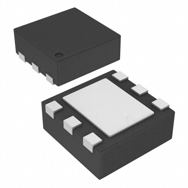
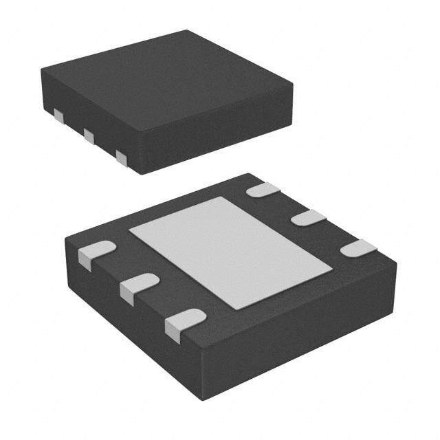
| 封装/外壳 | 6-WDFN 裸露焊盘 |
| 封装/箱体 | WSON-6 |
| 工作温度 | -40°C ~ 85°C |
| 工作温度范围 | - 40 C to + 85 C |
| 工厂包装数量 | 250 |
| 开关频率 | 2.25 MHz |
| 拓扑结构 | Buck |
| 最大工作温度 | + 85 C |
| 最大输入电压 | 6 V |
| 最小工作温度 | - 40 C |
| 最小输入电压 | 2 V |
| 标准包装 | 1 |
| 电压-输入 | 2 V ~ 6 V |
| 电压-输出 | 0.6 V ~ 6 V |
| 电流-输出 | 600mA |
| 类型 | 降压(降压) |
| 系列 | TPS62260 |
| 设计资源 | http://www.digikey.com/product-highlights/cn/zh/texas-instruments-webench-design-center/3176 |
| 输入电压 | 2 V to 6 V |
| 输出数 | 1 |
| 输出电压 | 0.6 V to 6 V |
| 输出电流 | 600 mA |
| 输出端数量 | 1 Output |
| 输出类型 | 可调式 |
| 配用 | /product-detail/zh/TPS62260LED-338/296-23400-ND/1850198/product-detail/zh/TPS62260EVM-229/296-31254-ND/1908048 |
| 频率-开关 | 2.25MHz |


- 商务部:美国ITC正式对集成电路等产品启动337调查
- 曝三星4nm工艺存在良率问题 高通将骁龙8 Gen1或转产台积电
- 太阳诱电将投资9.5亿元在常州建新厂生产MLCC 预计2023年完工
- 英特尔发布欧洲新工厂建设计划 深化IDM 2.0 战略
- 台积电先进制程称霸业界 有大客户加持明年业绩稳了
- 达到5530亿美元!SIA预计今年全球半导体销售额将创下新高
- 英特尔拟将自动驾驶子公司Mobileye上市 估值或超500亿美元
- 三星加码芯片和SET,合并消费电子和移动部门,撤换高东真等 CEO
- 三星电子宣布重大人事变动 还合并消费电子和移动部门
- 海关总署:前11个月进口集成电路产品价值2.52万亿元 增长14.8%


PDF Datasheet 数据手册内容提取
Product Sample & Technical Tools & Support & Reference Folder Buy Documents Software Community Design TPS62260,TPS62261,TPS62262,TPS62263 SLVS763E–JUNE2007–REVISEDJULY2015 TPS6226x 2.25-MHz 600-mA Step Down Converter in 2 x 2 WSON and SOT Package 1 Features With an wide input voltage range of 2 V to 6 V, the device also supports two- and three-cell alkaline • HighEfficiencyStep-DownConverter 1 batteries,3.3-Vand5-Vinputvoltagerails. • OutputCurrentupto600mA The TPS6226x operates at 2.25-MHz fixed-switching • V Rangefrom2Vto6VforLi-ionBatterieswith IN frequency, and enters power save mode operation at ExtendedVoltageRange light load currents to maintain high efficiency over the • 2.25-MHzFixedFrequencyOperation entireloadcurrentrange. • PowerSaveModeatLightLoadCurrents The power save mode is optimized for low-output • OutputVoltageAccuracyinPWMMode±1.5% voltage ripple. For low noise applications, the device can be forced into fixed frequency pulse-width • Typical15-μAQuiescentCurrent modulation (PWM) mode by pulling the MODE pin • 100%DutyCycleforLowestDropout high. In the shutdown mode, the current consumption • VoltagePositioningatLightLoads is reduced to less than 1 μA. The TPS6226x allows • AvailableinaSOT(5)and2-mm ×2-mm ×0.8- theuseofsmallinductorsandcapacitorstoachievea smallsolutionsize. mmWSON(6)Package • Allows<1-mmSolutionHeight The TPS6226x operates over a free air temperature range of –40°C to 85°C. It is available in a 5-pin SOT 2 Applications anda6-pin2-mm×2-mmWSONpackage. • MobilePhones,SmartPhones DeviceInformation(1) • LowPowerDSPSupply PARTNUMBER PACKAGE BODYSIZE(NOM) • PortableMediaPlayers WSON(6) 2.00mm×2.00mm TPS62260 • Point-of-Load(POL)Applications SOT(5) 2.90mm×1.60mm TPS62261 WSON(6) 2.00mm×2.00mm 3 Description WSON(6) 2.00mm×2.00mm The TPS6226x device is a highly efficient TPS62262 SOT(5) 2.90mm×1.60mm synchronous step-down DC/DC converter. The TPS62263 WSON(6) 2.00mm×2.00mm TPS6226x provides up to 600-mA output current from a single Li-Ion cell, and is ideal for battery-powered (1) For all available packages, see the orderable addendum at applications such as mobile phones and other theendofthedatasheet. portableequipment. space space space TypicalApplicationSchematic EfficiencyvsOutputCurrent VIN= 2 V to 6 V TPS62260DRV 2.2LmH Up to 600 mA 100% CIN VEINN SW R1 C221 pF COUVTOUT 9800%% VI =V 2I.7= V2.3 V 4.7mF 10mF 70% VI = 4.5 V MGONDDE FB R2 Efficiency 456000%%% VI =V 3I =V 3.6 V 30% 20% VMOO=D E1. 8= VGND 10% L= 2.2μH DCR = 110 mΩ 0% 10μ 100μ 1m 10m 100m 1 Output Current (A) 1 An IMPORTANT NOTICE at the end of this data sheet addresses availability, warranty, changes, use in safety-critical applications, intellectualpropertymattersandotherimportantdisclaimers.PRODUCTIONDATA.
TPS62260,TPS62261,TPS62262,TPS62263 SLVS763E–JUNE2007–REVISEDJULY2015 www.ti.com Table of Contents 1 Features.................................................................. 1 8.4 DeviceFunctionalModes..........................................9 2 Applications........................................................... 1 9 ApplicationandImplementation........................ 11 3 Description............................................................. 1 9.1 ApplicationInformation............................................11 4 RevisionHistory..................................................... 2 9.2 TypicalApplication..................................................11 9.3 SystemExamples...................................................19 5 DeviceComparisonTable..................................... 3 10 PowerSupplyRecommendations..................... 20 6 PinConfigurationandFunctions......................... 3 11 Layout................................................................... 20 7 Specifications......................................................... 4 11.1 LayoutGuidelines.................................................20 7.1 AbsoluteMaximumRatings......................................4 11.2 LayoutExamples...................................................20 7.2 ESDRatings..............................................................4 12 DeviceandDocumentationSupport................. 22 7.3 RecommendedOperatingConditions.......................4 7.4 ThermalInformation..................................................4 12.1 DeviceSupport......................................................22 7.5 ElectricalCharacteristics...........................................5 12.2 RelatedLinks........................................................22 7.6 TypicalCharacteristics..............................................6 12.3 CommunityResources..........................................22 12.4 Trademarks...........................................................22 8 DetailedDescription.............................................. 7 12.5 ElectrostaticDischargeCaution............................22 8.1 Overview...................................................................7 12.6 Glossary................................................................22 8.2 FunctionalBlockDiagram.........................................7 13 Mechanical,Packaging,andOrderable 8.3 FeatureDescription...................................................7 Information........................................................... 22 4 Revision History NOTE:Pagenumbersforpreviousrevisionsmaydifferfrompagenumbersinthecurrentversion. ChangesfromRevisionD(February2011)toRevisionE Page • AddedPinConfigurationandFunctionssection,ESDRatingstable,FeatureDescriptionsection,DeviceFunctional Modes,ApplicationandImplementationsection,PowerSupplyRecommendationssection,Layoutsection,Device andDocumentationSupportsection,andMechanical,Packaging,andOrderableInformationsection .............................. 1 2 SubmitDocumentationFeedback Copyright©2007–2015,TexasInstrumentsIncorporated ProductFolderLinks:TPS62260 TPS62261 TPS62262 TPS62263
TPS62260,TPS62261,TPS62262,TPS62263 www.ti.com SLVS763E–JUNE2007–REVISEDJULY2015 5 Device Comparison Table PARTNUMBER VOOLUTTAPGUET(1) PACKAGE(2) DEPSAICGKNAAGTEOR MODEPIN PMAACRKKAINGGE WSON(6) DRV Yes BYK TPS62260 Adjustable SOT(5) DDC No,PFM/PWMauto BYP transition TPS62261 1.8Vfixed WSON(6) DRV Yes BYL WSON(6) DRV Yes BYM TPS62262 1.2Vfixed SOT(5) DDC No,PFM/PWMauto QXS transition TPS62263 2.5Vfixed WSON(6) DRV Yes CFX (1) ContactTIforotherfixedoutputvoltageoptions (2) Forthemostcurrentpackageandorderinginformation,seeMechanical,Packaging,andOrderableInformation,orseetheTIwebsiteat www.ti.com. 6 Pin Configuration and Functions DDCPackage 5-PinSOT TopView V 1 5 SW IN GND 2 EN 3 4 FB DRVPackage 6-PinWSON TopView D SW 1 A 6 GND P MODE 2 er 5 VIN w FB 3 Po 4 EN PinFunctions PIN I/O DESCRIPTION NAME WSON SOT Thisistheenablepinofthedevice.Pullingthispintolowforcesthedeviceintoshutdown EN 4 3 IN mode.Pullingthispintohighenablesthedevice.Thispinmustbeterminated. Feedbackpinfortheinternalregulationloop.Connecttheexternalresistordividertothispin. FB 3 4 IN Incaseoffixedoutputvoltageoption,connectthispindirectlytotheoutputcapacitor GND 6 2 PWR GNDsupplypin. ThispinisonlyavailableatWSONpackageoption.MODEpin=Highforcesthedeviceto MODE 2 — IN operateinfixedfrequencyPWMmode.MODEpin=Lowenablesthepowersavemodewith automatictransitionfromPFMmodetofixedfrequencyPWMmode. ThisistheswitchpinandisconnectedtotheinternalMOSFETswitches.Connecttheexternal SW 1 5 OUT inductorbetweenthisterminalandtheoutputcapacitor. VIN 5 1 PWR V powersupplypin. IN Copyright©2007–2015,TexasInstrumentsIncorporated SubmitDocumentationFeedback 3 ProductFolderLinks:TPS62260 TPS62261 TPS62262 TPS62263
TPS62260,TPS62261,TPS62262,TPS62263 SLVS763E–JUNE2007–REVISEDJULY2015 www.ti.com 7 Specifications 7.1 Absolute Maximum Ratings Overoperatingfree-airtemperaturerange(unlessotherwisenoted)(1) MAX MIN UNIT V Inputvoltage (2) –0.3 7 IN VoltageatEN,MODE –0.3 V +0.3≤7 V IN VoltageonSW –0.3 7 Peakoutputcurrent Internallylimited A T Maximumoperatingjunctiontemperature –40 125 °C J T Storagetemperature –65 150 °C stg (1) StressesbeyondthoselistedunderAbsoluteMaximumRatingsmaycausepermanentdamagetothedevice.Thesearestressratings onlyandfunctionaloperationofthedeviceattheseoranyotherconditionsbeyondthoseindicatedunderrecommendedoperating conditionsisnotimplied.Exposuretoabsolute-maximum-ratedconditionsforextendedperiodsmayaffectdevicereliability. (2) Allvoltagevaluesarewithrespecttonetworkgroundterminal. 7.2 ESD Ratings VALUE UNIT Humanbodymodel(HBM),perANSI/ESDA/JEDECJS-001,allpins(1) ±2000 V(ESD) Electrostaticdischarge Chargeddevicemodel(CDM),perJEDECspecificationJESD22-C101, ±1000 V allpins(2) (1) JEDECdocumentJEP155statesthat500-VHBMallowssafemanufacturingwithastandardESDcontrolprocess. (2) JEDECdocumentJEP157statesthat250-VCDMallowssafemanufacturingwithastandardESDcontrolprocess. 7.3 Recommended Operating Conditions MIN NOM MAX UNIT V Supplyvoltage 2 6 V IN Outputvoltagerangeforadjustablevoltage 0.6 V V IN T Operatingambienttemperature –40 85 °C A T Operatingjunctiontemperature –40 125 °C J 7.4 Thermal Information TPS62260, TPS62260, TPS62261, TPS62262 TPS62262, THERMALMETRIC(1) TPS62263 UNIT DRV[WSON] DDC[SOT] 6PINS 5PINS R Junction-to-ambientthermalresistance 67.8 226.9 °C/W θJA R Junction-to-case(top)thermalresistance 88.5 40.7 °C/W θJC(top) R Junction-to-boardthermalresistance 37.2 48.8 °C/W θJB ψ Junction-to-topcharacterizationparameter 2.0 0.5 °C/W JT ψ Junction-to-boardcharacterizationparameter 37.6 48.1 °C/W JB R Junction-to-case(bottom)thermalresistance 7.9 n/a °C/W θJC(bot) (1) Formoreinformationabouttraditionalandnewthermalmetrics,seetheSemiconductorandICPackageThermalMetricsapplication report,SPRA953. 4 SubmitDocumentationFeedback Copyright©2007–2015,TexasInstrumentsIncorporated ProductFolderLinks:TPS62260 TPS62261 TPS62262 TPS62263
TPS62260,TPS62261,TPS62262,TPS62263 www.ti.com SLVS763E–JUNE2007–REVISEDJULY2015 7.5 Electrical Characteristics Overfulloperatingambienttemperaturerange,typicalvaluesareatT =25°C.Unlessotherwisenoted,specificationsapply A forconditionV =EN=3.6V.ExternalcomponentsC =4.7μF0603,C =10μF0603,L=2.2μH,seetheparameter IN IN OUT measurementinformation. PARAMETER TESTCONDITIONS MIN TYP MAX UNIT SUPPLY V Inputvoltagerange 2.3 6 V IN V 2.5Vto6V 600 IN I Outputcurrent V 2.3Vto2.5V 300 mA OUT IN V 2Vto2.3V 150 IN I =0mA,PFMmodeenabled OUT 15 (MODE=GND)devicenotswitching I =0mA,PFMmodeenabled μA OUT (MODE=GND)deviceswitching,V =1.8V, 18.5 IQ Operatingquiescentcurrent see (1) OUT I =0mA,switchingwithnoload OUT (MODE=V ),PWMoperation,V =1.8V, 3.8 mA IN OUT V =3V IN I Shutdowncurrent EN=GND 0.1 1 μA SD Falling 1.85 UVLO Undervoltagelockoutthreshold V Rising 1.95 ENABLE,MODE Highlevelinputvoltage,EN, 2V≤V ≤6V 1 VIN V IN V IH MODE Lowlevelinputvoltage,EN, 2V≤V ≤6V 0 0.4 V IN V IL MODE I Inputbiascurrent,EN,MODE EN,MODE=GNDorVIN 0.01 1 μA IN POWERSWITCH HighsideMOSFETon-resistance 240 480 R V =V =3.6V,T =25°C mΩ DS(on) IN GS A LowsideMOSFETon-resistance 185 380 ForwardcurrentlimitMOSFET I V =V =3.6V 0.8 1 1.2 A LIMF highsideandlowside IN GS Thermalshutdown Increasingjunctiontemperature 140 T °C SD Thermalshutdownhysteresis Decreasingjunctiontemperature 20 OSCILLATOR f Oscillatorfrequency 2V≤V ≤6V 2 2.25 2.5 MHz SW IN OUTPUT V Adjustableoutputvoltagerange 0.6 V V OUT IN V Referencevoltage 600 mV REF MODE=V ,PWMoperation,forfixedoutput IN FeedbackvoltagePWMmode voltageversionsV =V , –1.5% 0% 1.5% FB OUT 2.5V≤V ≤6V,0mA≤I ≤600mA (2) IN OUT V FB MODE=GND,deviceinPFMmode,voltage FeedbackvoltagePFMmode positioningactive(1) 1% Loadregulation PWMmode –0.5 %/A TimefromactiveENtoreach95%ofV 500 t Start-uptime OUT μs StartUp nominal t V ramp-uptime Timetorampfrom5%to95%ofV 250 μs Ramp OUT OUT I LeakagecurrentintoSWpin V =3.6V,V =V =V ,EN=GND (3) 0.1 1 μA lkg IN IN OUT SW (1) InPFMmode,theinternalreferencevoltageissettotyp.1.01×V .Seetheparametermeasurementinformation. REF (2) ForV =V +0.6V. IN OUT (3) Infixedoutputvoltageversions,theinternalresistordividernetworkisdisconnectedfromFBpin. Copyright©2007–2015,TexasInstrumentsIncorporated SubmitDocumentationFeedback 5 ProductFolderLinks:TPS62260 TPS62261 TPS62262 TPS62263
TPS62260,TPS62261,TPS62262,TPS62263 SLVS763E–JUNE2007–REVISEDJULY2015 www.ti.com 7.6 Typical Characteristics 0.8 20 EN = GND MODE = GND 0.7 EN = VIN TA= 85°C A) 18 Device Not Switching μ N ( 0.6 A) down Current Into VI 0000....3245 TA= 85°C Quiescent Current(μ 111246 TA=T A25=°–C40°C Shut 0.1 TA= 25°C TA=–40°C 10 0 8 2 2.5 3 3.5 4 4.5 5 5.5 6 2 2.5 3 3.5 4 4.5 5 5.5 6 Input Voltage (V) Input Voltage (V) Figure1.ShutdownCurrentIntoVINvsInputVoltage Figure2.QuiescentCurrentvsInputVoltage ()Ω 0.8 High Side Switching ()Ω 0.4 Low Side Switching nc 0.7 nc 0.35 a a esist 0.6 esist 0.3 R R State 0.5 TA= 85°C State 0.25 TA= 85°C On- 0.4 On- 0.2 e e urc 0.3 urc 0.15 o o n-S 0.2 TA=–40°C n-S 0.1 atic Drai 0.1 TA= 25°C atic Drai 0.05 TA=–40°C TA= 25°C St 0 St 0 2 2.5 3 3.5 4 4.5 5 2 2.5 3 3.5 4 4.5 5 Input Voltage (V) Input Voltage (V) Figure3.StaticDrain-SourceOn-StateResistancevsInput Figure4.StaticDrain-SourceOn-StateResistancevsInput Voltage Voltage 6 SubmitDocumentationFeedback Copyright©2007–2015,TexasInstrumentsIncorporated ProductFolderLinks:TPS62260 TPS62261 TPS62262 TPS62263
TPS62260,TPS62261,TPS62262,TPS62263 www.ti.com SLVS763E–JUNE2007–REVISEDJULY2015 8 Detailed Description 8.1 Overview The TPS6226x step-down converter operates with typically 2.25-MHz fixed frequency pulse-width modulation (PWM) at moderate to heavy load currents. At light load currents, the converter can automatically enter power savemodeandoperateinpulse-frequencymodulation(PFM)mode. During PWM operation, the converter uses a unique fast-response voltage mode control scheme with input voltage feed-forward to achieve good line and load regulation, allowing the use of small ceramic input and output capacitors. At the beginning of each clock cycle initiated by the clock signal, the high-side MOSFET switch is turned on. The current then flows from the input capacitor, through the high-side MOSFET switch, through the inductor, and to the output capacitor and load. During this phase, the current ramps up until the PWM comparator trips and the control logic turns off the switch. The current limit comparator also turns off the switch if the current limit of the high-side MOSFET switch is exceeded. After a dead time preventing shoot-through current, the low-side MOSFET rectifier is turned on and the inductor current ramps down. The current then flows from the inductor to the output capacitor and to the load. It returns back to the inductor through the low-side MOSFETrectifier. The next cycle is initiated by the clock signal, turning off the low-side MOSFET rectifier and turning on the high- sideMOSFETswitch. 8.2 Functional Block Diagram V IN Current- Limit Comparator V Thermal Undervoltage IN Shutdown Lockout1.8V Limit EN High Side PFM Comparator Reference +1%Voltage positioning 0.6V VREF FB VREF+1% Only in 2x2SON Gate Driver MODE MODE Control ShootA-Tnhtir-ough ErrorAmplifier Stage Softstart SW1 VOUTRAMP VREF CONTROL Integrator FB FB PWM Zero-Pole Comp. Amp. Limit RI1 GND Low Side RI..N RI3 Sawtooth 2.25-MHz CLiumrrite Cnto-mparator Generator Oscillator Int.Resistor Network GND 8.3 Feature Description 8.3.1 DynamicVoltagePositioning This feature reduces the voltage undershoots/overshoots at load steps from light to heavy load and vice versa. It is active in power save mode and regulates the output voltage 1% higher than the nominal value. This provides moreheadroomforboththevoltagedropataloadstep,andthevoltageincreaseataloadthrow-off. Copyright©2007–2015,TexasInstrumentsIncorporated SubmitDocumentationFeedback 7 ProductFolderLinks:TPS62260 TPS62261 TPS62262 TPS62263
TPS62260,TPS62261,TPS62262,TPS62263 SLVS763E–JUNE2007–REVISEDJULY2015 www.ti.com Feature Description (continued) Output voltage Vout +1% Voltage Positioning PFM Comparator threshold Light load PFM Mode Vout (PWM) moderate to heavy load PWM Mode Figure5. PowerSaveModeOperationWithAutomaticModeTransition 8.3.2 UndervoltageLockout The undervoltage lockout circuit prevents the device from malfunctioning at low input voltages and from excessive discharge of the battery and disables the output stage of the converter. The undervoltage lockout thresholdistypically1.85VwithfallingV . IN 8.3.3 ModeSelection TheMODEpinallowsmodeselectionbetweenforcedPWMmodeandpowersavemode. Connecting this pin to GND enables the power save mode with automatic transition between PWM and PFM mode. Pulling the MODE pin high forces the converter to operate in fixed frequency PWM mode even at light loadcurrents.Thisallowssimplefilteringoftheswitchingfrequencyfornoisesensitiveapplications.Inthismode, theefficiencyislowercomparedtothepowersavemodeduringlightloads. The condition of the MODE pin can be changed during operation and allows efficient power management by adjustingtheoperationmodeoftheconvertertothespecificsystemrequirements. 8.3.4 Enable The device is enabled by setting the EN pin to high. During the start up time t the internal circuits are Start Up settled and the soft start circuit is activated. The EN input can be used to control power sequencing in a system with various DC/DC converters. The EN pin can be connected to the output of another converter, to drive the EN pin high and getting a sequencing of supply rails. With EN = GND, the device enters shutdown mode in which all internal circuits are disabled. In fixed output voltage versions, the internal resistor divider network is then disconnectedfromFBpin. 8.3.5 ThermalShutdown As soon as the junction temperature, T , exceeds 140°C (typical) the device goes into thermal shutdown. In this J mode, the high side and low side MOSFETs are turned off. The device continues its operation when the junction temperaturefallsbelowthethermalshutdownhysteresis. 8 SubmitDocumentationFeedback Copyright©2007–2015,TexasInstrumentsIncorporated ProductFolderLinks:TPS62260 TPS62261 TPS62262 TPS62263
TPS62260,TPS62261,TPS62262,TPS62263 www.ti.com SLVS763E–JUNE2007–REVISEDJULY2015 8.4 Device Functional Modes 8.4.1 Soft-Start The TPS6226x has an internal soft start circuit that controls the ramp up of the output voltage. The output voltage ramps up from 5% to 95% of its nominal value within typical 250 μs. This limits the inrush current in the converter during ramp up and prevents possible input voltage drops when a battery or high impedance power sourceisused.Thesoftstartcircuitisenabledwithinthestartuptimet . StartUp 8.4.2 PowerSaveMode ThepowersavemodeisenabledwithMODEpinsettolowlevel.Iftheloadcurrentdecreases,theconverterwill enter power save mode operation automatically. During power save mode the converter skips switching and operateswithreducedfrequencyinPFMmodewithaminimumquiescentcurrenttomaintainhighefficiency.The converterwillpositiontheoutputvoltagetypically+1%abovethenominaloutputvoltage.Thisvoltagepositioning featureminimizesvoltagedropscausedbyasuddenloadstep. The transition from PWM mode to PFM mode occurs once the inductor current in the low side MOSFET switch becomeszero,whichindicatesdiscontinuousconductionmode. During the power save mode the output voltage is monitored with a PFM comparator. As the output voltage falls below the PFM comparator threshold of V nominal +1%, the device starts a PFM current pulse. The high side OUT MOSFETswitchwillturnon,andtheinductorcurrentrampsup.Aftertheon-timeexpires,theswitchisturnedoff andthelowsideMOSFETswitchisturnedonuntiltheinductorcurrentbecomeszero. The converter effectively delivers a current to the output capacitor and the load. If the load is below the delivered current,theoutputvoltagewillrise.IftheoutputvoltageisequaltoorhigherthanthePFMcomparatorthreshold, thedevicestopsswitchingandentersasleepmodewithtypical15-μAcurrentconsumption. If the output voltage is still below the PFM comparator threshold, a sequence of further PFM current pulses are generated until the PFM comparator threshold is reached. The converter starts switching again once the output voltagedropsbelowthePFMcomparatorthreshold. With a fast single threshold comparator, the output voltage ripple during PFM mode operation can be kept small. The PFM pulse is time controlled, which allows to modify the charge transferred to the output capacitor by the value of the inductor. The resulting PFM output voltage ripple and PFM frequency depend in first order on the size of the output capacitor and the inductor value. Increasing output capacitor values and inductor values will minimize the output ripple. The PFM frequency decreases with smaller inductor values and increases with larger values. The PFM mode is left and PWM mode entered in case the output current can not longer be supported in PFM mode. The power save mode can be disabled through the MODE pin set to high. The converter will then operate infixedfrequencyPWMmode. 8.4.3 100%DutyCycleLowDropoutOperation The device starts to enter 100% duty cycle mode once the input voltage comes close to the nominal output voltage.Inordertomaintaintheoutputvoltage,thehighsideMOSFETswitchisturnedon100%foroneormore cycles. With further decreasing V the high side MOSFET switch is turned on completely. In this case the converter IN offers a low input-to-output voltage difference. This is particularly useful in battery-powered applications to achievelongestoperationtimebytakingfulladvantageofthewholebatteryvoltagerange. The minimum input voltage to maintain regulation depends on the load current and output voltage, and can be calculatedas: V min=V max+I max×(R max+R ) IN OUT OUT DS(on) L where • I max=Maximumoutputcurrentplusinductorripplecurrent OUT • R max=MaximumP-channelswitchR DS(on) DS(on) • R =DCresistanceoftheinductor L • V max=Nominaloutputvoltageplusmaximumoutputvoltagetolerance (1) OUT Copyright©2007–2015,TexasInstrumentsIncorporated SubmitDocumentationFeedback 9 ProductFolderLinks:TPS62260 TPS62261 TPS62262 TPS62263
TPS62260,TPS62261,TPS62262,TPS62263 SLVS763E–JUNE2007–REVISEDJULY2015 www.ti.com Device Functional Modes (continued) 8.4.4 Short-CircuitProtection The high side and low side MOSFET switches are short-circuit protected with maximum switch current equal to I . The current in the switches is monitored by current limit comparators. Once the current in the high side LIMF MOSFET switch exceeds the threshold of its current limit comparator, it turns off and the low side MOSFET switch is activated to ramp down the current in the inductor and high side MOSFET switch. The high side MOSFET switch can only turn on again, once the current in the low side MOSFET switch has decreased below thethresholdofitscurrentlimitcomparator. 10 SubmitDocumentationFeedback Copyright©2007–2015,TexasInstrumentsIncorporated ProductFolderLinks:TPS62260 TPS62261 TPS62262 TPS62263
TPS62260,TPS62261,TPS62262,TPS62263 www.ti.com SLVS763E–JUNE2007–REVISEDJULY2015 9 Application and Implementation NOTE Information in the following applications sections is not part of the TI component specification, and TI does not warrant its accuracy or completeness. TI’s customers are responsible for determining suitability of components for their purposes. Customers should validateandtesttheirdesignimplementationtoconfirmsystemfunctionality. 9.1 Application Information The TPS6226x device is a high-efficiency synchronous step-down DC/DC converter featuring power save mode or2.25MHzfixedfrequencyoperation. 9.2 Typical Application TPS62260DRV L 1 2.2mH V 1.2 V OUT VIN SW R C C 1 1 C IN EN 360 kW 22 pF OUT 4.7mF 10mF FB GND R 2 360 kW MODE Figure6. TPS62260DRVAdjustable1.2-VOutput 9.2.1 DesignRequirements The device operates over an input voltage range from 2 V to 6 V. The output voltage is adjustable using an externalfeedbackdivider. 9.2.2 DetailedDesignProcedure Table1.ListofComponents COMPONENTREFERENCE PARTNUMBER MANUFACTURER VALUE C GRM188R60J475K Murata 4.7μF,6.3V.X5RCeramic IN C GRM188R60J106M Murata 10μF,6.3V.X5RCeramic OUT C Murata 22pF,COGCeramic 1 L LPS3015 Coilcraft 2.2μH,110mΩ 1 R ,R Valuesdependingontheprogrammedoutputvoltage 1 2 9.2.2.1 OutputVoltageSetting Theoutputvoltagecanbecalculatedto: æ R ö VOUT = VREF´ç1+R1÷ è 2øwithaninternalreferencevoltageV typical0.6V. REF To minimize the current through the feedback divider network, R should be 180 kΩ or 360 kΩ. The sum of R 2 1 andR shouldnotexceed~1MΩ,tokeepthenetworkrobustagainstnoise. 2 AnexternalfeedforwardcapacitorC isrequiredforoptimumloadtransientresponse.ThevalueofC shouldbe 1 1 intherangebetween22pFand33pF. Copyright©2007–2015,TexasInstrumentsIncorporated SubmitDocumentationFeedback 11 ProductFolderLinks:TPS62260 TPS62261 TPS62262 TPS62263
TPS62260,TPS62261,TPS62262,TPS62263 SLVS763E–JUNE2007–REVISEDJULY2015 www.ti.com RoutetheFBlineawayfromnoisesources,suchastheinductorortheSWline. 9.2.2.2 OutputFilterDesign(InductorandOutputCapacitor) The TPS6226x is designed to operate with inductors in the range of 1.5 μH to 4.7 μH and with output capacitors in the range of 4.7 μF to 22 μF. The part is optimized for operation with a 2.2-μH inductor and 10-μF output capacitor. Larger or smaller inductor values can be used to optimize the performance of the device for specific operation conditions. For stable operation, the L and C values of the output filter may not fall below 1-μH effective inductanceand3.5-μFeffectivecapacitance. Selecting larger capacitors is less critical because the corner frequency of the L-C filter moves to lower frequencieswithfewerstabilityproblems. 9.2.2.2.1 InductorSelection The inductor value has a direct effect on the ripple current. The selected inductor has to be rated for its DC resistance and saturation current. The inductor ripple current (ΔI ) decreases with higher inductance and L increaseswithhigherV orV . IN OUT The inductor selection also has an impact on the output voltage ripple in the PFM mode. Higher inductor values will lead to lower output voltage ripple and higher PFM frequency, lower inductor values will lead to a higher outputvoltageripplebutlowerPFMfrequency. Equation 2 calculates the maximum inductor current in PWM mode under static load conditions. The saturation current of the inductor should be rated higher than the maximum inductor current as calculated with Equation 3. This is recommended because during heavy load transient the inductor current will rise above the calculated value. V 1- OUT V DI = V ´ IN L OUT L´ƒ where • f=Switchingfrequency(2.25-MHztypical) • L=Inductorvalue • ΔI =Peak-to-peakinductorripplecurrent (2) L DI I max =I max+ L L OUT 2 where • ΔI =Peak-to-peakinductorripplecurrent L • I =Maximuminductorcurrent (3) Lmax A more conservative approach is to select the inductor current rating just for the maximum switch current limit I oftheconverter. LIMF Accepting larger values of ripple current allows the use of lower inductance values, but results in higher output voltageripple,greatercorelosses,andloweroutputcurrentcapability. The total losses of the coil have a strong impact on the efficiency of the DC/DC conversion and consist of both thelossesinthedcresistance(R )andthefollowingfrequency-dependentcomponents: (DC) • Thelossesinthecorematerial(magnetichysteresisloss,especiallyathighswitchingfrequencies) • Additionallossesintheconductorfromtheskineffect(currentdisplacementathighfrequencies) • Magneticfieldlossesoftheneighboringwindings(proximityeffect) • Radiationlosses 12 SubmitDocumentationFeedback Copyright©2007–2015,TexasInstrumentsIncorporated ProductFolderLinks:TPS62260 TPS62261 TPS62262 TPS62263
TPS62260,TPS62261,TPS62262,TPS62263 www.ti.com SLVS763E–JUNE2007–REVISEDJULY2015 Table2.ListofInductors DIMENSIONS[mm3] InductanceμH INDUCTORTYPE SUPPLIER 2.5×2.0×1.0max 2.0 MIPS2520D2R2 FDK 2.5×2.0×1.2max 2.0 MIPSA2520D2R2 FDK 2.5×2.0×1.0max 2.2 KSLI-252010AG2R2 HtachiMetals 2.5×2.0×1.2max 2.2 LQM2HPN2R2MJ0L Murata 3×3×1.5max 2.2 LPS30152R2 Coilcraft 9.2.2.2.2 OutputCapacitorSelection The advanced fast-response voltage mode control scheme of the TPS6226x allows the use of tiny ceramic capacitors. Ceramic capacitors with low ESR values have the lowest output voltage ripple and are recommended. The output capacitor requires either an X7R or X5R dielectric. Y5V and Z5U dielectric capacitors, asidefromtheirwidevariationincapacitanceovertemperature,becomeresistiveathighfrequencies. Atnominalloadcurrent,thedeviceoperatesinPWMmodeandtheRMSripplecurrentiscalculatedas: V 1- OUT V 1 I = V ´ IN ´ RMSCOUT OUT L´ƒ 2´ 3 (4) Atnominalloadcurrent,thedeviceoperatesinPWMmodeandtheoveralloutputvoltagerippleisthesumofthe voltagespikecausedbytheoutputcapacitorESRplusthevoltageripplecausedbycharginganddischargingthe outputcapacitor: V 1- OUT V æ 1 ö DV = V ´ IN ´ç +ESR÷ OUT OUT L´ƒ è8´COUT´ƒ ø (5) At light load currents, the converter operates in power save mode and the output voltage ripple is dependent on the output capacitor and inductor value. Larger output capacitor and inductor values minimize the voltage ripple inPFMmodeandtightenDCoutputaccuracyinPFMmode. 9.2.2.2.3 InputCapacitorSelection An input capacitor is required for best input voltage filtering, and minimizing the interference with other circuits caused by high input voltage spikes. For most applications, a 4.7-μF to 10-μF ceramic capacitor is recommended. Because ceramic capacitor loses up to 80% of its initial capacitance at 5 V, it is recommended that 10-μF input capacitors be used for input voltages >4.5 V. The input capacitor can be increased without any limit for better input voltage filtering. Take care when using only small ceramic input capacitors. When a ceramic capacitor is used at the input and the power is being supplied through long wires, such as from a wall adapter, a load step at the output or V step on the input can induce ringing at the VIN pin. This ringing can couple to the IN outputandbemistakenasloopinstabilityorcouldevendamagethepartbyexceedingthemaximumratings. Table3.ListofCapacitors CAPACITANCE TYPE SIZE SUPPLIER 4.7μF GRM188R60J475K 06031.6×0.8×0.8mm3 Murata 10μF GRM188R60J106M69D 06031.6×0.8×0.8mm3 Murata Table1showsthelistofcomponentsfortheApplicationCurves. Copyright©2007–2015,TexasInstrumentsIncorporated SubmitDocumentationFeedback 13 ProductFolderLinks:TPS62260 TPS62261 TPS62262 TPS62263
TPS62260,TPS62261,TPS62262,TPS62263 SLVS763E–JUNE2007–REVISEDJULY2015 www.ti.com 9.2.3 ApplicationCurves 100% 100% 90% VI = 2.3 V 90% VI = 2.3 V V = 2.7 V 80% I 80% V = 2.7 V I V = 4.5 V 70% I 70% V = 3 V ncy 60% VI = 3.6 V ncy 60% I VI = 3.6 V cie 50% VI = 3 V cie 50% Effi 40% Effi 40% V = 4.5 V I 30% 30% V = 1.8 V 20% MOODE = GND 20% VO= 1.8 V 10% L= 2.2μH 10% MODE = VI DCR = 110 mΩ L= 2.2μH 0% 0% 10μ 100μ 1m 10m 100m 1 1m 10m 100m 1 Output Current (A) Output Current (A) Figure7.Efficiency(PowerSaveMode)vsOutputCurrent Figure8.Efficiency(PWMMode)vsOutputCurrent 100% 100% 90% V = 4.2 V 90% V = 3.6 V I I 80% 80% V = 3.6 V V = 5 V I I 70% 70% V = 5 V cy 60% I cy 60% VI = 4.5 V n n Efficie 4500%% VI = 4.5 V Efficie 4500%% VI = 4.2 V 30% VO= 3.3 V 30% VO= 3.3 V MODE = VI MODE = GND 20% L= 2.2μH 20% L= 2.2μH DCR = 110 mΩ DCR = 110 mΩ 10% C = 10μF 0603 10% C = 10μF 0603 O O 0% 0% 1m 10m 100m 1 10μ 100μ 1m 10m 100m 1 Output Current (A) Output Current (A) Figure9.Efficiency(PWMMode)vsOutputCurrent Figure10.Efficiency(PowerSaveMode)vsOutput Current 100% 100% 90% 90% V = 2.3 V I V = 2.7 V 80% I 80% V = 4.5 V 70% V = 2.3 V 70% I I V = 3.6 V I ncy 60% VI = 4.5 V ncy 60% Efficie 4500%% Efficie 4500%% VI = 2.7 V V = 3.6 V I V = 1.2 V V = 1.2 V 30% O 30% O MODE = V MODE = GND I 20% L= 2μH 20% L= 2μH MIPSA2520 MIPSA2520 10% CO= 10μF 0603 10% CO= 10μF 0603 0% 0% 1m 10m 100m 1 10μ 100μ 1m 10m 100m 1 Output Current (A) Output Current (A) Figure11.EfficiencyvsOutputCurrent Figure12.EfficiencyvsOutputCurrent 14 SubmitDocumentationFeedback Copyright©2007–2015,TexasInstrumentsIncorporated ProductFolderLinks:TPS62260 TPS62261 TPS62262 TPS62263
TPS62260,TPS62261,TPS62262,TPS62263 www.ti.com SLVS763E–JUNE2007–REVISEDJULY2015 1.88 1.88 1.86 1.86 PFM Mode, Voltage Positioning PFM Mode, Voltage Positioning V) 1.84 V) 1.84 C ( C ( D D Output Voltage 111...788802 VI = 2.3 VVI =V 2I.7= V 3 V VI = 3V.6I V= 4.5 VTVAO== 215.8°C VMPWodMe Output Voltage 111...788802 VI = 2.3 VVI =V 2I.7= V3 V VI = 3V.I6 =V 4.5 V TVAO== –14.80 °VMPCWodMe MODE = GND MODE = GND 1.76 L= 2.2μH 1.76 L= 2.2μH C = 10μF C = 10μF O O 1.74 1.74 10μ 100μ 1m 10m 100m 1 10μ 100μ 1m 10m 100m 1 Output Current (A) Output Current (A) Figure13.OutputVoltageAccuracyvsOutputCurrent Figure14.OutputVoltageAccuracy(PowerSaveMode)vs OutputCurrent 1.88 1.854 T = 25°C A 1.86 1.836 VO= 1.8 V PFM Mode, Voltage Positioning MODE = VI V) 1.84 V) L= 2.2μH C ( C ( 1.818 D D e 1.82 e g PWM g Output Volta 11..7880 VI = 2 VVI =V 2I.7= V3 V VI = 3V.I6 =V 4.5 V TVAO== 815.8°C MVode Output Volta 1.718.28 VI = 2.3 VVI =V 2I.7= V3 V VI = 3V.I6 =V 4.5 V MODE = GND 1.764 1.76 L= 2.2μH C = 10μF O 1.74 1.746 10μ 100μ 1m 10m 100m 1 10μ 100μ 1m 10m 100m 1 Output Current (A) Output Current (A) Figure15.OutputVoltageAccuracy(PowerSaveMode)vs Figure16.OutputVoltageAccuracy(PWMMode)vs OutputCurrent OutputCurrent 1.854 1.854 T =–40°C T = 85°C A A V = 1.8 V V = 1.8 V 1.836 O 1.836 O MODE = V MODE = V I I V) L= 2.2μH V) L= 2.2μH C ( 1.818 C ( 1.818 D D e e g g a 1.8 a 1.8 olt olt ut V VI = 2 V VI = 3 V VI = 4.5 V ut V V = 2.3 V V = 3 V V = 4.5 V p 1.782 p 1.782 I I I ut V = 2.7 V V = 3.6 V ut O I I O V = 2.7 V V = 3.6 V I I 1.764 1.764 1.746 1.746 10μ 100μ 1m 10m 100m 1 10μ 100μ 1m 10m 100m 1 Output Current (A) Output Current (A) Figure17.OutputVoltageAccuracy(PWMMode)vs Figure18.OutputVoltageAccuracy(PWMMode)vs OutputCurrent OutputCurrent Copyright©2007–2015,TexasInstrumentsIncorporated SubmitDocumentationFeedback 15 ProductFolderLinks:TPS62260 TPS62261 TPS62262 TPS62263
TPS62260,TPS62261,TPS62262,TPS62263 SLVS763E–JUNE2007–REVISEDJULY2015 www.ti.com VI= 3.6 V VO(20 mV/Div) V = 1.8 V, I = 150 mA O O VO(10 mV/Div) L= 2.2μH, CO= 10μF 0603 V = 3.6 V I V = 1.8 V, I = 10 mA SW (2 V/Div) O O L= 2.2μH, C = 10μF O I (200 mA/Div) SW (2 V/Div) COIL I (200 mA/Div) COIL Time Base (10μs/Div) Time Base (10μs/Div) Figure19.TypicalOperation(PWMMode) Figure20.TypicalOperation(PFMMode) V = 3.6 V V = 3.6 V I I MODE V = 1.8 V V = 1.8 V O O (2 V/Div) I = 10 mA MODE (2 V/Div) IO= 10 mA O SW (2 V/Div) SW (2 V/Div) PFM Mode Forced PWM Mode Forced PWM Mode PFM Mode I COIL (200 mA/Div) I COIL (200 mA/Div) Time Base (1μs/Div) Time Base (2.5μs/Div) Figure21.ModePinTransitionfromPFM Figure22.ModePinTransitionfromPWM toForcedPWMModeatLightLoad toPFMModeatLightLoad V= 3.6 V I EN V = 1.5 V (2 V/Div) VO(50 mV/Div) IO= 50 mAto 200 mA O MODE = VIN SW (2 V/Div) IO(200 mA/Div) 200 mA VO(2 V/Div) 50 mA I (500 mA/Div) COIL I (100 mA/Div) I V = 3.6 V, R = 10Ω I L V = 1.8 V, I into C O I I MODE = GND Time Base (100μs/Div) Time Base (20μs/Div) Figure23.Start-UpTiming Figure24.LoadTransient(ForcedPWMMode) 16 SubmitDocumentationFeedback Copyright©2007–2015,TexasInstrumentsIncorporated ProductFolderLinks:TPS62260 TPS62261 TPS62262 TPS62263
TPS62260,TPS62261,TPS62262,TPS62263 www.ti.com SLVS763E–JUNE2007–REVISEDJULY2015 V= 3.6 V I VO(50 mV/Div) VIO== 2 10.05 mVAto 400 mA SW (2 V/Div) O V= 3.6 V I (200 mA/Div) 400 mA I O VO(50 mV/Div) VO= 1.5 V I = 150μAto 400 mA O 200 mA MODE = GND I (500 mA/Div) 400 mA O ICOIL(500 mA/Div) 150μA I (500 mA/Div) COIL Time Base (20μs/Div) Time Base (500μs/Div) Figure25.LoadTransient(ForcedPWMMode) Figure26.LoadTransient(PFMModetoPWMMode) SW (2 V/Div) SW (2 V/Div) VI= 3.6 V VI= 3.6 V VO= 1.5 V VO= 1.5 V IMOO=D 1E5 0= μGANtDo 400 mA IMOO=D 1E.5 = m GANtDo 50 mA VO(50 mV/Div) V (50 mV/Div) O 400 mA 50 mA IO(500 mA/Div) IO(50 mA/Div) 150μA 1.5 mA I (500 mA/Div) COIL I (500 mA/Div) COIL Time Base (500μs/Div) Time Base (50μs/Div) Figure27.LoadTransient(PWMModetoPFMMode) Figure28.LoadTransient(PFMMode) SW (2 V/Div) SW (2 V/Div) V= 3.6 V I V = 1.5 V O V (50 mV/Div) IO= 50 mAto 1.5 mA VO(50 mV/Div) O MODE = GND V= 3.6 V I V = 1.8 V O I = 50 mAto 250 mA O MODE = GND 250 mA 50 mA I (50 mA/Div) O I (200 mA/Div) 50 mA O 1.5 mA I (500 mA/Div) I (500 mA/Div) COIL COIL Time Base (50μs/Div) Time Base (20μs/Div) Figure29.LoadTransient(PFMMode) Figure30.LoadTransient(PFMModetoPWMMode) Copyright©2007–2015,TexasInstrumentsIncorporated SubmitDocumentationFeedback 17 ProductFolderLinks:TPS62260 TPS62261 TPS62262 TPS62263
TPS62260,TPS62261,TPS62262,TPS62263 SLVS763E–JUNE2007–REVISEDJULY2015 www.ti.com SW (2 V/Div) V= 3.6 V I VO(50 mV/Div) VO= 1.5 V I = 50 mAto 400 mA O MODE = GND PFM Mode PWM Mode 400 mA I (500 mA/Div) O 50 mA I (500 mA/Div) COIL Time Base (20μs/Div) Figure31.LoadTransient(PFMModetoPWMMode) Figure32.LoadTransient(PWMModetoPFMMode) V = 3.6 V to 4.2 V V = 3.6 V to 4.2 V I I (500 mV/Div) (500 mV/Div) V = 1.8 V O V = 1.8 V (50 mV/Div) O I = 50 mA (50 mV/Div) O I = 250 mA MODE = GND O MODE = VIN Time Base (100μs/Div) Time Base (100μs/Div) Figure33.LineTransient(PFMMode) Figure34.LineTransient(ForcedPWMMode) 18 SubmitDocumentationFeedback Copyright©2007–2015,TexasInstrumentsIncorporated ProductFolderLinks:TPS62260 TPS62261 TPS62262 TPS62263
TPS62260,TPS62261,TPS62262,TPS62263 www.ti.com SLVS763E–JUNE2007–REVISEDJULY2015 9.3 System Examples 9.3.1 TPS62260,Adjustable1.5-VOutput TPS62260DRV L1 V 1.5 V OUT VIN= 2 V to 6 V 2.2mH Up to 600 mA VIN SW C R1 C1 IN EN 540 kΩ 22 pF 4.7mF C FB OUT GND 10mF R2 360 kΩ MODE Figure35. TPS62260Adjustable1.5-VOutput 9.3.2 TPS62262,Fixed1.2-VOutput TPS62262DRV L1 V 1.2 V OUT V = 2 V to 6 V 2.2mH Up to 600 mA IN VIN SW C C IN EN OUT 4.7mF 10mF FB GND MODE Figure36. TPS62262Fixed1.2-VOutput 9.3.3 TPS62261,Fixed1.8-VOutput TPS62261DRV L1 VOUT1.8 V V = 2 V to 6 V 2.2mH Up to 600 mA IN VIN SW C IN EN 4.7mF C OUT FB 10mF GND MODE Figure37. TPS62261Fixed1.8-VOutput Copyright©2007–2015,TexasInstrumentsIncorporated SubmitDocumentationFeedback 19 ProductFolderLinks:TPS62260 TPS62261 TPS62262 TPS62263
TPS62260,TPS62261,TPS62262,TPS62263 SLVS763E–JUNE2007–REVISEDJULY2015 www.ti.com 10 Power Supply Recommendations The TPS6226x device has no special requirements for its input power supply. The input power supply output currentmustberatedaccordingtothesupplyvoltage,outputvoltage,andoutputcurrentoftheTPS6226x. 11 Layout 11.1 Layout Guidelines As for all switching power supplies, the layout is an important step in the design. Proper function of the device demands careful attention to PCB layout. Care must be taken in board layout to get the specified performance. If the layout is not carefully done, the regulator could show poor line and/or load regulation, and additional stability issues as well as EMI problems. It is critical to provide a low inductance, impedance ground path. Therefore, use wide and short traces for the main current paths. The input capacitor should be placed as close as possible to theICpinsaswellastheinductorandoutputcapacitor. Connect the GND pin of the device to the PowerPAD™ land of the PCB and use this pad as a star point. Use a common power GND node and a different node for the signal GND to minimize the effects of ground noise. Connect these ground nodes together to the PowerPAD land (star point) underneath the IC. Keep the common path to the GND pin, which returns the small signal components and the high current of the output capacitors as shortaspossibletoavoidgroundnoise.TheFBlineshouldbeconnectedrighttotheoutputcapacitorandrouted awayfromnoisycomponentsandtraces(forexample,theSWline). 11.2 Layout Examples Figure38. SuggestedLayoutforFixedOutputVoltageOptions 20 SubmitDocumentationFeedback Copyright©2007–2015,TexasInstrumentsIncorporated ProductFolderLinks:TPS62260 TPS62261 TPS62262 TPS62263
TPS62260,TPS62261,TPS62262,TPS62263 www.ti.com SLVS763E–JUNE2007–REVISEDJULY2015 Layout Examples (continued) GND V OUT 2 C1 R V R1 IN C OUT N L CI U D N G Figure39. SuggestedLayoutforAdjustableOutputVoltageVersion Copyright©2007–2015,TexasInstrumentsIncorporated SubmitDocumentationFeedback 21 ProductFolderLinks:TPS62260 TPS62261 TPS62262 TPS62263
TPS62260,TPS62261,TPS62262,TPS62263 SLVS763E–JUNE2007–REVISEDJULY2015 www.ti.com 12 Device and Documentation Support 12.1 Device Support 12.1.1 Third-PartyProductsDisclaimer TI'S PUBLICATION OF INFORMATION REGARDING THIRD-PARTY PRODUCTS OR SERVICES DOES NOT CONSTITUTE AN ENDORSEMENT REGARDING THE SUITABILITY OF SUCH PRODUCTS OR SERVICES OR A WARRANTY, REPRESENTATION OR ENDORSEMENT OF SUCH PRODUCTS OR SERVICES, EITHER ALONEORINCOMBINATIONWITHANYTIPRODUCTORSERVICE. 12.2 Related Links The table below lists quick access links. Categories include technical documents, support and community resources,toolsandsoftware,andquickaccesstosampleorbuy. Table4.RelatedLinks TECHNICAL TOOLS& SUPPORT& PARTS PRODUCTFOLDER SAMPLE&BUY DOCUMENTS SOFTWARE COMMUNITY TPS62260 Clickhere Clickhere Clickhere Clickhere Clickhere TPS62261 Clickhere Clickhere Clickhere Clickhere Clickhere TPS62262 Clickhere Clickhere Clickhere Clickhere Clickhere TPS62263 Clickhere Clickhere Clickhere Clickhere Clickhere 12.3 Community Resources The following links connect to TI community resources. Linked contents are provided "AS IS" by the respective contributors. They do not constitute TI specifications and do not necessarily reflect TI's views; see TI's Terms of Use. TIE2E™OnlineCommunity TI'sEngineer-to-Engineer(E2E)Community.Createdtofostercollaboration amongengineers.Ate2e.ti.com,youcanaskquestions,shareknowledge,exploreideasandhelp solveproblemswithfellowengineers. DesignSupport TI'sDesignSupport QuicklyfindhelpfulE2Eforumsalongwithdesignsupporttoolsand contactinformationfortechnicalsupport. 12.4 Trademarks PowerPAD,E2EaretrademarksofTexasInstruments. Allothertrademarksarethepropertyoftheirrespectiveowners. 12.5 Electrostatic Discharge Caution Thesedeviceshavelimitedbuilt-inESDprotection.Theleadsshouldbeshortedtogetherorthedeviceplacedinconductivefoam duringstorageorhandlingtopreventelectrostaticdamagetotheMOSgates. 12.6 Glossary SLYZ022—TIGlossary. Thisglossarylistsandexplainsterms,acronyms,anddefinitions. 13 Mechanical, Packaging, and Orderable Information The following pages include mechanical, packaging, and orderable information. This information is the most current data available for the designated devices. This data is subject to change without notice and revision of thisdocument.Forbrowser-basedversionsofthisdatasheet,refertotheleft-handnavigation. 22 SubmitDocumentationFeedback Copyright©2007–2015,TexasInstrumentsIncorporated ProductFolderLinks:TPS62260 TPS62261 TPS62262 TPS62263
PACKAGE OPTION ADDENDUM www.ti.com 4-Jul-2020 PACKAGING INFORMATION Orderable Device Status Package Type Package Pins Package Eco Plan Lead finish/ MSL Peak Temp Op Temp (°C) Device Marking Samples (1) Drawing Qty (2) Ball material (3) (4/5) (6) TPS62260DDCR ACTIVE SOT-23-THIN DDC 5 3000 Green (RoHS NIPDAU Level-1-260C-UNLIM -40 to 85 BYP & no Sb/Br) TPS62260DDCRG4 ACTIVE SOT-23-THIN DDC 5 3000 Green (RoHS NIPDAU Level-1-260C-UNLIM -40 to 85 BYP & no Sb/Br) TPS62260DDCT ACTIVE SOT-23-THIN DDC 5 250 Green (RoHS NIPDAU Level-1-260C-UNLIM -40 to 85 BYP & no Sb/Br) TPS62260DDCTG4 ACTIVE SOT-23-THIN DDC 5 250 Green (RoHS NIPDAU Level-1-260C-UNLIM -40 to 85 BYP & no Sb/Br) TPS62260DRVR ACTIVE WSON DRV 6 3000 Green (RoHS Call TI | NIPDAUAG Level-1-260C-UNLIM -40 to 85 BYK & no Sb/Br) TPS62260DRVT ACTIVE WSON DRV 6 250 Green (RoHS Call TI | NIPDAUAG Level-1-260C-UNLIM -40 to 85 BYK & no Sb/Br) TPS62260DRVTG4 ACTIVE WSON DRV 6 250 Green (RoHS NIPDAUAG Level-1-260C-UNLIM -40 to 85 BYK & no Sb/Br) TPS62261DRVR ACTIVE WSON DRV 6 3000 Green (RoHS NIPDAU Level-1-260C-UNLIM -40 to 85 BYL & no Sb/Br) TPS62261DRVT ACTIVE WSON DRV 6 250 Green (RoHS NIPDAU Level-1-260C-UNLIM -40 to 85 BYL & no Sb/Br) TPS62262DDCR ACTIVE SOT-23-THIN DDC 5 3000 Green (RoHS NIPDAU Level-1-260C-UNLIM -40 to 85 QXS & no Sb/Br) TPS62262DDCT ACTIVE SOT-23-THIN DDC 5 250 Green (RoHS NIPDAU Level-1-260C-UNLIM -40 to 85 QXS & no Sb/Br) TPS62262DRVR ACTIVE WSON DRV 6 3000 Green (RoHS NIPDAUAG Level-1-260C-UNLIM -40 to 85 BYM & no Sb/Br) TPS62262DRVT ACTIVE WSON DRV 6 250 Green (RoHS NIPDAUAG Level-1-260C-UNLIM -40 to 85 BYM & no Sb/Br) TPS62263DRVR ACTIVE WSON DRV 6 3000 Green (RoHS NIPDAU Level-1-260C-UNLIM -40 to 85 CFX & no Sb/Br) TPS62263DRVT ACTIVE WSON DRV 6 250 Green (RoHS NIPDAU Level-1-260C-UNLIM -40 to 85 CFX & no Sb/Br) (1) The marketing status values are defined as follows: ACTIVE: Product device recommended for new designs. LIFEBUY: TI has announced that the device will be discontinued, and a lifetime-buy period is in effect. Addendum-Page 1
PACKAGE OPTION ADDENDUM www.ti.com 4-Jul-2020 NRND: Not recommended for new designs. Device is in production to support existing customers, but TI does not recommend using this part in a new design. PREVIEW: Device has been announced but is not in production. Samples may or may not be available. OBSOLETE: TI has discontinued the production of the device. (2) RoHS: TI defines "RoHS" to mean semiconductor products that are compliant with the current EU RoHS requirements for all 10 RoHS substances, including the requirement that RoHS substance do not exceed 0.1% by weight in homogeneous materials. Where designed to be soldered at high temperatures, "RoHS" products are suitable for use in specified lead-free processes. TI may reference these types of products as "Pb-Free". RoHS Exempt: TI defines "RoHS Exempt" to mean products that contain lead but are compliant with EU RoHS pursuant to a specific EU RoHS exemption. Green: TI defines "Green" to mean the content of Chlorine (Cl) and Bromine (Br) based flame retardants meet JS709B low halogen requirements of <=1000ppm threshold. Antimony trioxide based flame retardants must also meet the <=1000ppm threshold requirement. (3) MSL, Peak Temp. - The Moisture Sensitivity Level rating according to the JEDEC industry standard classifications, and peak solder temperature. (4) There may be additional marking, which relates to the logo, the lot trace code information, or the environmental category on the device. (5) Multiple Device Markings will be inside parentheses. Only one Device Marking contained in parentheses and separated by a "~" will appear on a device. If a line is indented then it is a continuation of the previous line and the two combined represent the entire Device Marking for that device. (6) Lead finish/Ball material - Orderable Devices may have multiple material finish options. Finish options are separated by a vertical ruled line. Lead finish/Ball material values may wrap to two lines if the finish value exceeds the maximum column width. Important Information and Disclaimer:The information provided on this page represents TI's knowledge and belief as of the date that it is provided. TI bases its knowledge and belief on information provided by third parties, and makes no representation or warranty as to the accuracy of such information. Efforts are underway to better integrate information from third parties. TI has taken and continues to take reasonable steps to provide representative and accurate information but may not have conducted destructive testing or chemical analysis on incoming materials and chemicals. TI and TI suppliers consider certain information to be proprietary, and thus CAS numbers and other limited information may not be available for release. In no event shall TI's liability arising out of such information exceed the total purchase price of the TI part(s) at issue in this document sold by TI to Customer on an annual basis. OTHER QUALIFIED VERSIONS OF TPS62260, TPS62261, TPS62262, TPS62263 : •Automotive: TPS62260-Q1, TPS62261-Q1, TPS62262-Q1, TPS62263-Q1 NOTE: Qualified Version Definitions: •Automotive - Q100 devices qualified for high-reliability automotive applications targeting zero defects Addendum-Page 2
PACKAGE MATERIALS INFORMATION www.ti.com 20-Jul-2019 TAPE AND REEL INFORMATION *Alldimensionsarenominal Device Package Package Pins SPQ Reel Reel A0 B0 K0 P1 W Pin1 Type Drawing Diameter Width (mm) (mm) (mm) (mm) (mm) Quadrant (mm) W1(mm) TPS62260DDCR SOT- DDC 5 3000 179.0 8.4 3.2 3.2 1.4 4.0 8.0 Q3 23-THIN TPS62260DDCT SOT- DDC 5 250 179.0 8.4 3.2 3.2 1.4 4.0 8.0 Q3 23-THIN TPS62260DRVR WSON DRV 6 3000 179.0 8.4 2.2 2.2 1.2 4.0 8.0 Q2 TPS62260DRVT WSON DRV 6 250 179.0 8.4 2.2 2.2 1.2 4.0 8.0 Q2 TPS62261DRVR WSON DRV 6 3000 179.0 8.4 2.2 2.2 1.2 4.0 8.0 Q2 TPS62261DRVT WSON DRV 6 250 179.0 8.4 2.2 2.2 1.2 4.0 8.0 Q2 TPS62262DDCR SOT- DDC 5 3000 179.0 8.4 3.2 3.2 1.4 4.0 8.0 Q3 23-THIN TPS62262DDCT SOT- DDC 5 250 180.0 8.4 3.2 3.2 1.4 4.0 8.0 Q3 23-THIN TPS62262DRVR WSON DRV 6 3000 179.0 8.4 2.2 2.2 1.2 4.0 8.0 Q2 TPS62262DRVT WSON DRV 6 250 179.0 8.4 2.2 2.2 1.2 4.0 8.0 Q2 TPS62263DRVR WSON DRV 6 3000 179.0 8.4 2.2 2.2 1.2 4.0 8.0 Q2 TPS62263DRVT WSON DRV 6 250 179.0 8.4 2.2 2.2 1.2 4.0 8.0 Q2 PackMaterials-Page1
PACKAGE MATERIALS INFORMATION www.ti.com 20-Jul-2019 *Alldimensionsarenominal Device PackageType PackageDrawing Pins SPQ Length(mm) Width(mm) Height(mm) TPS62260DDCR SOT-23-THIN DDC 5 3000 203.0 203.0 35.0 TPS62260DDCT SOT-23-THIN DDC 5 250 203.0 203.0 35.0 TPS62260DRVR WSON DRV 6 3000 203.0 203.0 35.0 TPS62260DRVT WSON DRV 6 250 203.0 203.0 35.0 TPS62261DRVR WSON DRV 6 3000 203.0 203.0 35.0 TPS62261DRVT WSON DRV 6 250 203.0 203.0 35.0 TPS62262DDCR SOT-23-THIN DDC 5 3000 203.0 203.0 35.0 TPS62262DDCT SOT-23-THIN DDC 5 250 203.0 203.0 35.0 TPS62262DRVR WSON DRV 6 3000 203.0 203.0 35.0 TPS62262DRVT WSON DRV 6 250 203.0 203.0 35.0 TPS62263DRVR WSON DRV 6 3000 203.0 203.0 35.0 TPS62263DRVT WSON DRV 6 250 203.0 203.0 35.0 PackMaterials-Page2
None
None
GENERIC PACKAGE VIEW DRV 6 WSON - 0.8 mm max height PLASTIC SMALL OUTLINE - NO LEAD Images above are just a representation of the package family, actual package may vary. Refer to the product data sheet for package details. 4206925/F
PACKAGE OUTLINE DRV0006A WSON - 0.8 mm max height SCALE 5.500 PLASTIC SMALL OUTLINE - NO LEAD B 2.1 A 1.9 PIN 1 INDEX AREA 2.1 1.9 0.8 C 0.7 SEATING PLANE 0.08 C (0.2) TYP 1 0.1 0.05 EXPOSED 0.00 THERMAL PAD 3 4 2X 7 1.3 1.6 0.1 6 1 4X 0.65 0.35 6X PIN 1 ID 0.3 0.25 6X (OPTIONAL) 0.2 0.1 C A B 0.05 C 4222173/B 04/2018 NOTES: 1. All linear dimensions are in millimeters. Any dimensions in parenthesis are for reference only. Dimensioning and tolerancing per ASME Y14.5M. 2. This drawing is subject to change without notice. 3. The package thermal pad must be soldered to the printed circuit board for thermal and mechanical performance. www.ti.com
EXAMPLE BOARD LAYOUT DRV0006A WSON - 0.8 mm max height PLASTIC SMALL OUTLINE - NO LEAD 6X (0.45) (1) 1 7 6X (0.3) 6 SYMM (1.6) (1.1) 4X (0.65) 4 3 (R0.05) TYP SYMM ( 0.2) VIA (1.95) TYP LAND PATTERN EXAMPLE SCALE:25X 0.07 MAX 0.07 MIN ALL AROUND ALL AROUND SOLDER MASK METAL METAL UNDER SOLDER MASK OPENING SOLDER MASK OPENING NON SOLDER MASK DEFINED SOLDER MASK (PREFERRED) DEFINED SOLDER MASK DETAILS 4222173/B 04/2018 NOTES: (continued) 4. This package is designed to be soldered to a thermal pad on the board. For more information, see Texas Instruments literature number SLUA271 (www.ti.com/lit/slua271). 5. Vias are optional depending on application, refer to device data sheet. If some or all are implemented, recommended via locations are shown. www.ti.com
EXAMPLE STENCIL DESIGN DRV0006A WSON - 0.8 mm max height PLASTIC SMALL OUTLINE - NO LEAD SYMM 6X (0.45) METAL 1 7 6X (0.3) 6 (0.45) SYMM 4X (0.65) (0.7) 4 3 (R0.05) TYP (1) (1.95) SOLDER PASTE EXAMPLE BASED ON 0.125 mm THICK STENCIL EXPOSED PAD #7 88% PRINTED SOLDER COVERAGE BY AREA UNDER PACKAGE SCALE:30X 4222173/B 04/2018 NOTES: (continued) 6. Laser cutting apertures with trapezoidal walls and rounded corners may offer better paste release. IPC-7525 may have alternate design recommendations. www.ti.com
PACKAGE OUTLINE DRV0006D WSON - 0.8 mm max height SCALE 5.500 PLASTIC SMALL OUTLINE - NO LEAD B 2.1 A 1.9 PIN 1 INDEX AREA 2.1 1.9 0.8 C 0.7 SEATING PLANE 0.08 C (0.2) TYP 1 0.1 0.05 EXPOSED 0.00 THERMAL PAD 3 4 2X 7 1.3 1.6 0.1 6 1 4X 0.65 0.35 6X PIN 1 ID 0.3 0.25 6X (OPTIONAL) 0.2 0.1 C A B 0.05 C 4225563/A 12/2019 NOTES: 1. All linear dimensions are in millimeters. Any dimensions in parenthesis are for reference only. Dimensioning and tolerancing per ASME Y14.5M. 2. This drawing is subject to change without notice. 3. The package thermal pad must be soldered to the printed circuit board for thermal and mechanical performance. www.ti.com
EXAMPLE BOARD LAYOUT DRV0006D WSON - 0.8 mm max height PLASTIC SMALL OUTLINE - NO LEAD 6X (0.45) (1) 1 7 6X (0.3) 6 SYMM (1.6) (1.1) 4X (0.65) 4 3 (R0.05) TYP SYMM ( 0.2) VIA (1.95) TYP LAND PATTERN EXAMPLE EXPOSED METAL SHOWN SCALE:25X 0.07 MAX 0.07 MIN ALL AROUND ALL AROUND EXPOSED EXPOSED METAL METAL SOLDER MASK METAL METAL UNDER SOLDER MASK OPENING SOLDER MASK OPENING NON SOLDER MASK DEFINED SOLDER MASK (PREFERRED) DEFINED SOLDER MASK DETAILS 4225563/A 12/2019 NOTES: (continued) 4. This package is designed to be soldered to a thermal pad on the board. For more information, see Texas Instruments literature number SLUA271 (www.ti.com/lit/slua271). 5. Vias are optional depending on application, refer to device data sheet. If some or all are implemented, recommended via locations are shown. www.ti.com
EXAMPLE STENCIL DESIGN DRV0006D WSON - 0.8 mm max height PLASTIC SMALL OUTLINE - NO LEAD SYMM 6X (0.45) METAL 1 7 6X (0.3) 6 (0.45) SYMM 4X (0.65) (0.7) 4 3 (R0.05) TYP (1) (1.95) SOLDER PASTE EXAMPLE BASED ON 0.125 mm THICK STENCIL EXPOSED PAD #7 88% PRINTED SOLDER COVERAGE BY AREA UNDER PACKAGE SCALE:30X 4225563/A 12/2019 NOTES: (continued) 6. Laser cutting apertures with trapezoidal walls and rounded corners may offer better paste release. IPC-7525 may have alternate design recommendations. www.ti.com
IMPORTANTNOTICEANDDISCLAIMER TI PROVIDES TECHNICAL AND RELIABILITY DATA (INCLUDING DATASHEETS), DESIGN RESOURCES (INCLUDING REFERENCE DESIGNS), APPLICATION OR OTHER DESIGN ADVICE, WEB TOOLS, SAFETY INFORMATION, AND OTHER RESOURCES “AS IS” AND WITH ALL FAULTS, AND DISCLAIMS ALL WARRANTIES, EXPRESS AND IMPLIED, INCLUDING WITHOUT LIMITATION ANY IMPLIED WARRANTIES OF MERCHANTABILITY, FITNESS FOR A PARTICULAR PURPOSE OR NON-INFRINGEMENT OF THIRD PARTY INTELLECTUAL PROPERTY RIGHTS. These resources are intended for skilled developers designing with TI products. You are solely responsible for (1) selecting the appropriate TI products for your application, (2) designing, validating and testing your application, and (3) ensuring your application meets applicable standards, and any other safety, security, or other requirements. These resources are subject to change without notice. TI grants you permission to use these resources only for development of an application that uses the TI products described in the resource. Other reproduction and display of these resources is prohibited. No license is granted to any other TI intellectual property right or to any third party intellectual property right. TI disclaims responsibility for, and you will fully indemnify TI and its representatives against, any claims, damages, costs, losses, and liabilities arising out of your use of these resources. TI’s products are provided subject to TI’s Terms of Sale (www.ti.com/legal/termsofsale.html) or other applicable terms available either on ti.com or provided in conjunction with such TI products. TI’s provision of these resources does not expand or otherwise alter TI’s applicable warranties or warranty disclaimers for TI products. Mailing Address: Texas Instruments, Post Office Box 655303, Dallas, Texas 75265 Copyright © 2020, Texas Instruments Incorporated