ICGOO在线商城 > 集成电路(IC) > PMIC - 稳压器 - DC DC 开关稳压器 > TPS54339DDA
 Datasheet下载
- 型号: TPS54339DDA
- 制造商: Texas Instruments
- 库位|库存: xxxx|xxxx
- 要求:
| 数量阶梯 | 香港交货 | 国内含税 |
| +xxxx | $xxxx | ¥xxxx |
查看当月历史价格
查看今年历史价格
TPS54339DDA产品简介:
ICGOO电子元器件商城为您提供TPS54339DDA由Texas Instruments设计生产,在icgoo商城现货销售,并且可以通过原厂、代理商等渠道进行代购。 TPS54339DDA价格参考。Texas InstrumentsTPS54339DDA封装/规格:PMIC - 稳压器 - DC DC 开关稳压器, 可调式 降压 开关稳压器 IC 正 0.76V 1 输出 3A 8-PowerSOIC(0.154",3.90mm 宽)。您可以下载TPS54339DDA参考资料、Datasheet数据手册功能说明书,资料中有TPS54339DDA 详细功能的应用电路图电压和使用方法及教程。
TPS54339DDA 是 Texas Instruments(德州仪器)推出的一款高效同步降压 DC-DC 开关稳压器,适用于多种需要高效率、小尺寸和稳定电源输出的应用场景。以下是其主要应用场景:

1. 嵌入式系统
   TPS54339DDA 适合为嵌入式系统提供稳定的电源供应,例如工业自动化设备、物联网(IoT)网关和边缘计算设备。其宽输入电压范围(4.5V 至 60V)使其能够适应各种供电环境。

2. 通信设备
   在通信领域,该芯片可用于基站、路由器、交换机等设备的电源管理模块。其高效的转换能力(高达 96% 的效率)和低静态电流特性有助于降低功耗并提高系统的热性能。

3. 汽车电子
   TPS54339DDA 的宽电压输入范围和良好的瞬态响应性能,使其非常适合汽车电子应用,如信息娱乐系统、车载导航设备和高级驾驶辅助系统(ADAS)。此外,其过温保护和短路保护功能增强了系统的可靠性。

4. 消费类电子产品
   该芯片可用于笔记本电脑适配器、平板电脑和其他便携式设备的电源管理系统。其紧凑的封装(DDA 封装)和外部元件数量少的特点,使得设计更加灵活且节省空间。

5. 医疗设备
   在医疗领域,TPS54339DDA 可用于便携式医疗设备(如血糖仪、便携式超声设备)以及固定式医疗设备(如监护仪)。其高精度输出电压调节能力和低噪声特性确保了设备的稳定运行。

6. LED 驱动器
   由于其支持高达 3A 的连续输出电流,TPS54339DDA 还可以用于驱动高功率 LED,适用于路灯、背光显示和工业照明等场景。

7. 测试与测量设备
   在精密测试与测量仪器中,TPS54339DDA 提供的低纹波输出和快速瞬态响应性能,能够满足对电源质量要求较高的应用需求。

总之,TPS54339DDA 凭借其高性能、高可靠性和灵活性,广泛应用于工业、通信、汽车、消费电子和医疗等多个领域,为各类设备提供稳定且高效的电源解决方案。
| 参数 | 数值 |
| 产品目录 | 集成电路 (IC)半导体 |
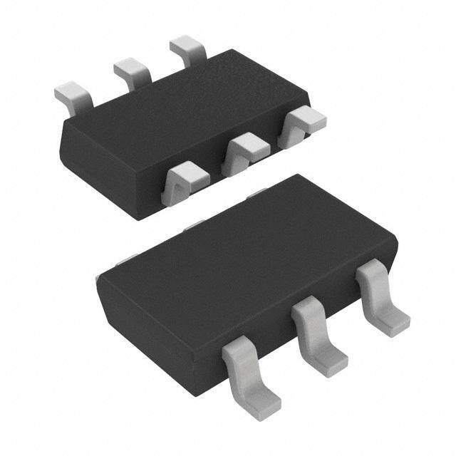
| 描述 | IC REG BUCK SYNC ADJ 3A 8SOPWR稳压器—开关式稳压器 4.5V to 23V Input 3A Sync SD Cnvtr |
| 产品分类 | |
| 品牌 | Texas Instruments |
| 产品手册 | |
| 产品图片 |
|
| rohs | 符合RoHS无铅 / 符合限制有害物质指令(RoHS)规范要求 |
| 产品系列 | 电源管理 IC,稳压器—开关式稳压器,Texas Instruments TPS54339DDASWIFT™, D-CAP2™ |
| 数据手册 | |
| 产品型号 | TPS54339DDA |
| PCN设计/规格 | |
| PWM类型 | 混合物 |
| 产品种类 | 稳压器—开关式稳压器 |
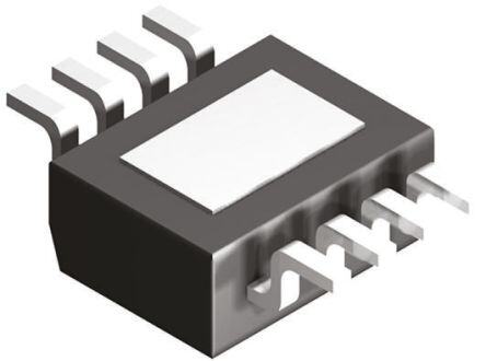
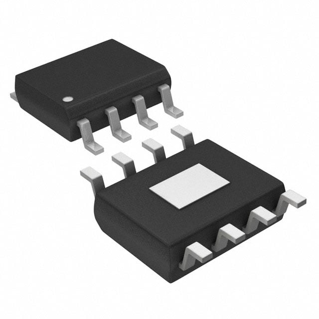
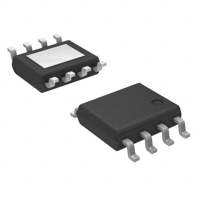
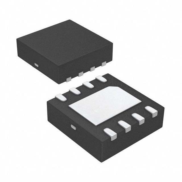
| 供应商器件封装 | 8-SO PowerPad |
| 包装 | 管件 |
| 同步整流器 | 是 |
| 商标 | Texas Instruments |
| 安装类型 | 表面贴装 |
| 安装风格 | SMD/SMT |
| 封装 | Tube |
| 封装/外壳 | 8-SOIC(0.154",3.90mm 宽)裸焊盘 |
| 封装/箱体 | HSOP-8 |
| 工作温度 | -40°C ~ 85°C |
| 工作温度范围 | - 40 C to + 85 C |
| 工厂包装数量 | 75 |
| 开关频率 | 600 kHz |
| 拓扑结构 | Buck |
| 最大工作温度 | + 85 C |
| 最大输入电压 | 23 V |
| 最小工作温度 | - 40 C |
| 最小输入电压 | 4.5 V |
| 标准包装 | 75 |
| 电压-输入 | 4.5 V ~ 23 V |
| 电压-输出 | 0.76 V ~ 7 V |
| 电流-输出 | 3A |
| 类型 | Step Down |
| 系列 | TPS54339 |
| 输入电压 | 4.5 V to 23 V |
| 输出数 | 1 |
| 输出电压 | 760 mV to 7 V |
| 输出电流 | 10 mA |
| 输出端数量 | 1 |
| 输出类型 | 可调式 |
| 频率-开关 | 600kHz |


- 商务部:美国ITC正式对集成电路等产品启动337调查
- 曝三星4nm工艺存在良率问题 高通将骁龙8 Gen1或转产台积电
- 太阳诱电将投资9.5亿元在常州建新厂生产MLCC 预计2023年完工
- 英特尔发布欧洲新工厂建设计划 深化IDM 2.0 战略
- 台积电先进制程称霸业界 有大客户加持明年业绩稳了
- 达到5530亿美元!SIA预计今年全球半导体销售额将创下新高
- 英特尔拟将自动驾驶子公司Mobileye上市 估值或超500亿美元
- 三星加码芯片和SET,合并消费电子和移动部门,撤换高东真等 CEO
- 三星电子宣布重大人事变动 还合并消费电子和移动部门
- 海关总署:前11个月进口集成电路产品价值2.52万亿元 增长14.8%


PDF Datasheet 数据手册内容提取
TPS54339 www.ti.com SLVSBT2–JANUARY2013 4.5 V to 23 V Input, 3-A Synchronous Step-Down SWIFT™ Converter CheckforSamples:TPS54339 FEATURES DESCRIPTION 1 • D-CAP2™ModeEnablesFastTransient The TPS54339 is an adaptive on-time D-CAP2™ 23 mode synchronous buck converter. The TPS54339 Response enables system designers to complete the suite of • LowOutputRippleandAllowsCeramicOutput various end-equipment power bus regulators with a Capacitor cost effective, low component count, low standby • WideV InputVoltageRange:4.5Vto23V current solution. The main control loop for the IN TPS54339 uses the D-CAP2™ mode control that • OutputVoltageRange:0.76Vto7V provides a fast transient response with no external • HighlyEfficientIntegratedFETsOptimized compensation components. The TPS54339 also has forLowerDutyCycleApplications a proprietary circuit that enables the device to adopt –140mΩ (HighSide)and70mΩ(LowSide) to both low equivalent series resistance (ESR) output • HighEfficiency,lessthan10μAatshutdown capacitors, such as POSCAP or SP-CAP, and ultra- low ESR ceramic capacitors. The device operates • HighInitialBandgapReferenceAccuracy from 4.5-V to 23-V VIN input. The output voltage can • AdjustableSoftStart be programmed between 0.76 V and 7 V. The device • Pre-BiasedSoftStart also features an adjustable soft start time. The TPS54339 is available in the 8-pin DDA package, • 600-kHzSwitchingFrequency(f ) SW anddesignedtooperatefrom–40°Cto85°C. • CycleByCycleOverCurrentLimit APPLICATIONS • WideRangeofApplicationsforLowVoltage System – DigitalTVPowerSupply – HighDefinitionBlu-rayDisc™Players – NetworkingHomeTerminal – DigitalSetTopBox(STB) VIN Vout (50 mV/div) TPS54339DDA 1 8 VBST SS 2 7 VIN EN EN VOUT 3 SW VREG5 6 Iout (2A/div) 4 5 GND VFB VOUT PwPd 9 100 us/div 1 Pleasebeawarethatanimportantnoticeconcerningavailability,standardwarranty,anduseincriticalapplicationsof TexasInstrumentssemiconductorproductsanddisclaimerstheretoappearsattheendofthisdatasheet. D-CAP2isatrademarkofTexasInstruments. 2 Blu-rayDiscisatrademarkofBlu-rayDiscAssociation. 3 PRODUCTIONDATAinformationiscurrentasofpublicationdate. Copyright©2013,TexasInstrumentsIncorporated Products conform to specifications per the terms of the Texas Instruments standard warranty. Production processing does not necessarilyincludetestingofallparameters.
TPS54339 SLVSBT2–JANUARY2013 www.ti.com Thesedeviceshavelimitedbuilt-inESDprotection.Theleadsshouldbeshortedtogetherorthedeviceplacedinconductivefoam duringstorageorhandlingtopreventelectrostaticdamagetotheMOSgates. ORDERINGINFORMATION(1) T PACKAGE(2) (3) ORDERABLEPARTNUMBER PIN TRANSPORT A MEDIA TPS54339DDA Tube –40°Cto85°C DDA 8 TPS54339DDAR TapeandReel (1) Forthemostcurrentpackageandorderinginformation,seethePackageOptionAddendumattheendofthisdocument,orseetheTI websiteatwww.ti.com. (2) Packagedrawings,thermaldata,andsymbolizationareavailableatwww.ti.com/packaging. (3) AllpackageoptionshaveCuNIPDAUlead/ballfinish. ABSOLUTE MAXIMUM RATINGS overoperatingfree-airtemperaturerange(unlessotherwisenoted) (1) VALUE UNIT MIN MAX VIN,EN –0.3 25 VBST –0.3 31 VBST(10nstransient) –0.3 33 Inputvoltagerange VBST(vsSW) –0.3 6.5 V VFB,SS –0.3 6.5 SW –2 25 SW(10nstransient) –3 27 VREG5 –0.3 6.5 Outputvoltagerange V GND –0.3 0.3 VoltagefromGNDtothermalpad,V –0.2 0.2 V diff HumanBodyModel(HBM) 2 kV Electrostaticdischarge ChargedDeviceModel(CDM) 500 V Operatingjunctiontemperature,T –40 150 J °C Storagetemperature,T –55 150 stg (1) Stressesbeyondthoselistedunderabsolutemaximumratingsmaycausepermanentdamagetothedevice.Thesearestressratings only,andfunctionaloperationofthedeviceattheseoranyotherconditionsbeyondthoseindicatedunderrecommendedoperating conditionsisnotimplied.Exposuretoabsolute-maximum-ratedconditionsforextendedperiodsmayaffectdevicereliability. THERMAL INFORMATION TPS54339 THERMALMETRIC(1) UNITS DDA(8PINS) θ Junction-to-ambientthermalresistance 46.2 JA θ Junction-to-case(top)thermalresistance 53.9 JCtop θ Junction-to-boardthermalresistance 29.7 JB °C/W ψ Junction-to-topcharacterizationparameter 10.0 JT ψ Junction-to-boardcharacterizationparameter 29.6 JB θ Junction-to-case(bottom)thermalresistance 6.6 JCbot (1) Formoreinformationabouttraditionalandnewthermalmetrics,seetheICPackageThermalMetricsapplicationreport,SPRA953. 2 SubmitDocumentationFeedback Copyright©2013,TexasInstrumentsIncorporated ProductFolderLinks:TPS54339
TPS54339 www.ti.com SLVSBT2–JANUARY2013 RECOMMENDED OPERATING CONDITIONS overoperatingfree-airtemperaturerange,(unlessotherwisenoted) MIN MAX UNIT V Supplyinputvoltagerange 4.5 23 V IN VBST –0.1 29 VBST(10nstransient) –0.1 32 VBST(vsSW) –0.1 5.7 SS –0.1 5.7 V Inputvoltagerange EN –0.1 23 V I VFB –0.1 5.5 SW –1.8 23 SW(10nstransient) –3 26 GND –0.1 0.1 V Outputvoltagerange VREG5 –0.1 5.7 V O I OutputCurrentrange I 0 10 mA O VREG5 T Operatingfree-airtemperature –40 85 °C A T Operatingjunctiontemperature –40 150 °C J ELECTRICAL CHARACTERISTICS overoperatingfree-airtemperaturerange,V =12V(unlessotherwisenoted) IN PARAMETER TESTCONDITIONS MIN TYP MAX UNIT SUPPLYCURRENT I Operating-non-switchingsupplycurrent V current,T =25°C,EN=5V,V =0.8V 850 1200 μA VIN IN A FB I Shutdownsupplycurrent V current,T =25°C,EN=0V 3.0 10 μA VINSDN IN A LOGICTHRESHOLD V ENhigh-levelinputvoltage EN 1.6 V ENH V ENlow-levelinputvoltage EN 0.6 V ENL R ENpinresistancetoGND V =12V 200 400 800 kΩ EN EN V VOLTAGEANDDISCHARGERESISTANCE FB T =25°C,V =1.05V,continuousmode V V thresholdvoltage A O 749 765 781 mV FBTH FB operation I V inputcurrent V =0.8V,T =25°C 0 ±0.1 μA VFB FB FB A V OUTPUT REG5 T =25°C,6.0V<V <23V, V V outputvoltage A IN 5.2 5.5 5.7 V VREG5 REG5 0<I <5mA VREG5 I Outputcurrent V =6V,V =4.0V,T =25°C 20 mA VREG5 IN REG5 A MOSFET R Highsideswitchresistance 25°C,V -SW=5.5V(1) 140 mΩ DS(on)h BST R Lowsideswitchresistance 25°C(1) 70 mΩ DS(on)l CURRENTLIMIT I Currentlimit Lout=2.2μH(1) 3.5 4.1 5.7 A ocl THERMALSHUTDOWN Shutdowntemperature (1) 165 T Thermalshutdownthreshold °C SDN Hysteresis (1) 40 ON-TIMETIMERCONTROL t Ontime V =12V,V =1.05V 160 ns ON IN O t Minimumofftime T =25°C,V =0.7V(1) 260 310 ns OFF(MIN) A FB (1) Notproductiontested. Copyright©2013,TexasInstrumentsIncorporated SubmitDocumentationFeedback 3 ProductFolderLinks:TPS54339
TPS54339 SLVSBT2–JANUARY2013 www.ti.com ELECTRICAL CHARACTERISTICS (continued) overoperatingfree-airtemperaturerange,V =12V(unlessotherwisenoted) IN PARAMETER TESTCONDITIONS MIN TYP MAX UNIT SOFTSTART I SSchargecurrent V =1.0V 4.2 6.0 7.8 μA SSC SS I SSdischargecurrent V =0.5V 0.8 1.5 mA SSD SS HICCUPANDOVERVOLTAGEPROTECTION V OutputOVPthreshold OVPDetect(L>H) 125% OVP V OutputHiccupthreshold Hiccupdetect(H>L) 65% UVP T OutputHiccupdelay toHiccupstate 6 µs UVPDEL T OutputHiccupEnabledelay Relativetosoft-starttime x1.7 UVPEN UVLO WakeupV voltage 3.45 3.75 4.05 REG5 UVLO UVLOthreshold V HysteresisV voltage 0.17 0.33 0.47 REG5 DEVICE INFORMATION DDAPACKAGE (TOPVIEW) 1 VBST SS 8 2 VIN EN 7 POWER PAD TPS54339 DDA 3 SW HSOP8 VREG5 6 4 GND VFB 5 PINFUNCTIONS PIN DESCRIPTION NAME NO. Supplyinputforthehigh-sideFETgatedrivecircuit.Connect0.1µFcapacitorbetweenVBSTandSWpins. VBST 1 AninternaldiodeisconnectedbetweenVREG5andVBST. VIN 2 Inputvoltagesupplypin. SW 3 Switchnodeconnectionbetweenhigh-sideNFETandlow-sideNFET. Groundpin.Powergroundreturnforswitchingcircuit.ConnectsensitiveSSandVFBreturnstoGNData GND 4 singlepoint. VFB 5 Converterfeedbackinput.Connecttooutputvoltagewithfeedbackresistordivider. 4 SubmitDocumentationFeedback Copyright©2013,TexasInstrumentsIncorporated ProductFolderLinks:TPS54339
TPS54339 www.ti.com SLVSBT2–JANUARY2013 PINFUNCTIONS(continued) PIN DESCRIPTION NAME NO. 5.5Vpowersupplyoutput.Acapacitor(typical0.47µF)shouldbeconnectedtoGND.VREG5isnotactive VREG5 6 whenENislow. EN 7 Enableinputcontrol.ENisactivehighandmustbepulleduptoenablethedevice. SS 8 Soft-startcontrol.AnexternalcapacitorshouldbeconnectedtoGND. Exposed Thermalpadofthepackage.Mustbesolderedtoachieveappropriatedissipation.Mustbeconnectedto Backside ThermalPad GND. FUNCTIONALBLOCKDIAGRAM SS 8 Softstart SS VBST 1 VIN SGND VIN EN EN 7 2 Logic VREG5 VREG5 Control Logic 6 OV 1 Shot SW 3 VO +25% XCON PGND VREG5 Ceramic Capacitor Ref SS PWM 4 5 GND VFB SW SGND OCP PGND VIN OV VREG5 Protection UVLO Logic UVLO TSD REF Ref Copyright©2013,TexasInstrumentsIncorporated SubmitDocumentationFeedback 5 ProductFolderLinks:TPS54339
TPS54339 SLVSBT2–JANUARY2013 www.ti.com OVERVIEW The TPS54339 is a 3-A synchronous step-down (buck) converter with two integrated N-channel MOSFETs. It operates using D-CAP2™ mode control. The fast transient response of D-CAP2™ control reduces the output capacitance required to meet a specific level of performance. Proprietary internal circuitry allows the use of low ESRoutputcapacitorsincludingceramicandspecialpolymertypes. DETAILED DESCRIPTION PWMOperation The main control loop of the TPS54339 is an adaptive on-time pulse width modulation (PWM) controller that supports a proprietary D-CAP2™ mode control. D-CAP2™ mode control combines constant on-time control with an internal compensation circuit for pseudo-fixed frequency and low external component count configuration with bothlowESRandceramicoutputcapacitors.Itisstableevenwithvirtuallynorippleattheoutput. At the beginning of each cycle, the high-side MOSFET is turned on. This MOSFET is turned off after internal one shot timer expires. This one shot is set by the converter input voltage, VIN, and the output voltage, VO, to maintain a pseudo-fixed frequency over the input voltage range, hence it is called adaptive on-time control. The one-shot timer is reset and the high-side MOSFET is turned on again when the feedback voltage falls below the reference voltage. An internal ramp is added to reference voltage to simulate output ripple, eliminating the need forESRinducedoutputripplefromD-CAP2™modecontrol. PWMFrequencyandAdaptiveOn-TimeControl TPS54339 uses an adaptive on-time control scheme and does not have a dedicated on board oscillator. The TPS54339 runs with a pseudo-constant frequency of 600 kHz by using the input voltage and output voltage to set the on-time one-shot timer. The on-time is inversely proportional to the input voltage and proportional to the outputvoltage;therefore,whenthedutyratioisVOUT/VIN,thefrequencyisconstant. SoftStartandPre-BiasedSoftStart The soft start function is adjustable. When the EN pin becomes high, 6 μA current begins charging the capacitor which is connected from the SS pin to GND. Smooth control of the output voltage is maintained during start up. The equation for the slow start time is shown in Equation 1. VFB voltage is 0.765 V and SS pin source current is 6μA. C (nF)xV ´1.1 C (nF)x0.765´1.1 SS REF SS t (ms)= = SS I (mA) 6 SS (1) The TPS54339 contains a unique circuit to prevent current from being pulled from the output during startup if the output is pre-biased. When the soft-start commands a voltage higher than the pre-bias level (internal soft start becomes greater than feedback voltage V ), the controller slowly activates synchronous rectification by starting FB the first low side FET gate driver pulses with a narrow on-time. It then increments that on-time on a cycle-by- cycle basis until it coincides with the time dictated by (1-D), where D is the duty cycle of the converter. This scheme prevents the initial sinking of the pre-bias output, and ensure that the out voltage (V ) starts and ramps O up smoothly into regulation and the control loop is given time to transition from pre-biased start-up to normal modeoperation. CurrentProtection The output overcurrent protection (OCP) is implemented using a cycle-by-cycle valley detect control circuit. The switch current is monitored by measuring the low-side FET switch voltage between the SW pin and GND. This voltage is proportional to the switch current. To improve accuracy, the voltage sensing is temperature compensated. During the on time of the high-side FET switch, the switch current increases at a linear rate determined by V , IN V , the on-time and the output inductor value. During the on time of the low-side FET switch, this current OUT decreases linearly. The average value of the switch current is the load current Iout. The TPS54339 constantly monitorsthelow-sideFETswitchvoltage,whichisproportionaltotheswitchcurrent,duringthelow-sideon-time. If the measured voltage is above the voltage proportional to the current limit, an internal counter is incremented per each SW cycle and the converter maintains the low-side switch on until the measured voltage is below the voltage corresponding to the current limit at which time the switching cycle is terminated and a new switching 6 SubmitDocumentationFeedback Copyright©2013,TexasInstrumentsIncorporated ProductFolderLinks:TPS54339
TPS54339 www.ti.com SLVSBT2–JANUARY2013 cycle begins. In subsequent switching cycles, the on-time is set to a fixed value and the current is monitored in the same manner. If the over current condition exists for 7 consecutive switching cycles, the internal OCL threshold is set to a lower level, reducing the available output current. When a switching cycle occurs where the switch current is not above the lower OCL threshold, the counter is reset and the OCL limit is returned to the highervalue. There are some important considerations for this type of over-current protection. The load current one half of the peak-to-peak inductor current higher than the over-current threshold. Also when the current is being limited, the output voltage tends to fall as the demanded load current may be higher than the current available from the converter. This may cause the output voltage to fall. When the VFB voltage becomes lower than 65% of the target voltage, the UVP comparator detects it. After 6µs detecting the UVP voltage, device will shut down and re- startafter7timesSSperiodforHiccup. When the over current condition is removed, the output voltage returns to the regulated value. This protection is non-latching. OverVoltageProtection TPS54339 detects over voltage conditions by monitoring the feedback voltage (VFB). This function is enabled afterapproximately1.7xtimesthesoftstarttime. When the feedback voltage becomes higher than 125% of the target voltage, the OVP comparator output goes high and both the high-side MOSFET driver and the low-side MOSFET driver turn off. This function is non-latch operation. UVLOProtection Undervoltage lock out protection (UVLO) monitors the voltage of the V pin. When the V voltage is lower REG5 REG5 thanUVLOthresholdvoltage,theTPS54339isshutoff.Thisprotectionisnon-latching. ThermalShutdown TPS54339 monitors the temperature of itself. If the temperature exceeds the threshold value (typically 165°C), thedeviceisshutoff.Thisisnon-latchprotection. Copyright©2013,TexasInstrumentsIncorporated SubmitDocumentationFeedback 7 ProductFolderLinks:TPS54339
TPS54339 SLVSBT2–JANUARY2013 www.ti.com TYPICAL CHARACTERISTICS VIN=12V,T =25°C(unlessotherwisenoted). A 1200 10 1000 A) (cid:29)Current (A) 680000 (cid:29)wn Current ( 68 y o Suppl 400 Shutd 4 –I CC 200 –I vccsdn 2 0 0 –50 0 50 100 150 –50 0 50 100 150 TJ – Junction Temperature ((cid:131)C) C001 TJ – Junction Temperature ((cid:131)C) C002 Figure1.VINCURRENTvsJUNCTIONTEMPERATURE Figure2.VINSHUTDOWNCURRENTvs JUNCTIONTEMPERATURE 80 1.100 V = 23 V IN (cid:29)ut Current (A) 4600 utput Voltage (V) 11..005705 VIN = 12 V VIN = 23 V p O EN In 20 – OUT1.025 VIN = 5 V V 0 1.000 0 5 10 15 20 25 0.0 0.5 1.0 1.5 2.0 2.5 3.0 EN Input Voltage (V) C003 IOUT – Output Current (A) C004 Figure3.ENCURRENTvsENVOLTAGE Figure4.1.05-VOUTPUTVOLTAGEvsOUTPUTCURRENT 1.07 I = 0 A e (V) 1.06 OUT Vout (50 mV/div) g a olt V ut 1.05 p ut – O IOUT = 1 A Iout (2A/div) UT1.04 O V 100 us/div 1.03 0 5 10 15 20 25 VIN – Input Voltage (V) C005 Figure5.1.05-VOUTPUTVOLTAGEvsINPUTVOLTAGE Figure6.1.05-V,LOADTRANSIENTRESPONSE 8 SubmitDocumentationFeedback Copyright©2013,TexasInstrumentsIncorporated ProductFolderLinks:TPS54339
TPS54339 www.ti.com SLVSBT2–JANUARY2013 TYPICAL CHARACTERISTICS VIN=12V,T =25°C(unlessotherwisenoted). A 100 90 EN (10 V/div) %) 80 VREG5 (5 V/div) ncy ( 70 VO = 1.8 V VO = 3.3 V VO = 5 V e ci Effi 60 Vout (0.5 V/div) 50 400 us/div 40 0.0 0.5 1.0 1.5 2.0 2.5 3.0 IOUT – Output Current (A) C006 Figure7.START-UPWAVEFORM Figure8.EFFICIENCYvsOUTPUTCURRENT 900 800 z) 850 z) 700 VO = 3.3 V H H k 800 k y ( y ( 600 Frequenc 677505000 VO = 5 V VO = 3.3 V VO = 1.8 V Frequenc 450000 VO = 1.05 V VO = 1.8 V g g hin 600 hin 300 c c wit 550 wit S S 200 – W500 VO = 1.2 V – W fS450 V = 1.05 V fS100 O 400 0 0 5 10 15 20 25 0.0 0.5 1.0 1.5 2.0 2.5 3.0 VIN – Input Voltage (V) C007 IOUT – Output Current (A) C008 Figure9.SWITCHINGFREQUENCYvs Figure10.SWITCHINGFREQUENCYvsOUTPUTCURRENT INPUTVOLTAGE(I =1A) O 0.780 I = 1 A OUT Vo = 1.05 V 0.775 Vo (10 mV/div) V) 0.770 e ( g olta 0.765 SW (5 V/div) V B VF 0.760 0.755 400 ns/div 0.750 –50 0 50 100 150 TJ – Junction Temperature ((cid:131)C) C009 Figure11.VFBVOLTAGEvsJUNCTION Figure12.VOLTAGERIPPLEATOUTPUT(I =3A) O TEMPERATURE(I =1A) O Copyright©2013,TexasInstrumentsIncorporated SubmitDocumentationFeedback 9 ProductFolderLinks:TPS54339
TPS54339 SLVSBT2–JANUARY2013 www.ti.com TYPICAL CHARACTERISTICS (continued) VIN=12V,T =25°C(unlessotherwisenoted). A Vo = 1.05 V VIN (50 mV/div) SW (5 V/div) 400 ns/div Figure13.VOLTAGERIPPLEATINPUT(I =3A) O 10 SubmitDocumentationFeedback Copyright©2013,TexasInstrumentsIncorporated ProductFolderLinks:TPS54339
TPS54339 www.ti.com SLVSBT2–JANUARY2013 DESIGN GUIDE Step-By-StepDesignProcedure Tobeginthedesignprocess,theusermustknowafewapplicationparameters: • Inputvoltagerange • Outputvoltage • Outputcurrent • Outputvoltageripple • Inputvoltageripple VIN 4.5to23V VIN C1 C2 C3 10μF 10μF 0.1μF U1 TPS54339DDA R3 10.0kΩ 7 2 EN EN VIN 5 1 C7 0.1μF VOUT VOUT VFB VBST R1 8.25kΩ 6 3 L1 1.05V3A VOUT R2 VREG5 SW 22.1kΩ 8 4 2.2μH C4 1 C5 SS GND C8 C9 C10 0.47μF PwrPAD 1 C6 9 22μF 22μF 8200pF 1 Not Installed Figure14. Showstheschematicdiagramforthisdesignexample. OutputVoltageResistorsSelection The output voltage is set with a resistor divider from the output node to the VFB pin. It is recommended to use 1%toleranceorbetterdividerresistors.StartbyusingEquation2tocalculateV . OUT To improve efficiency at light loads consider using larger value resistors, high resistance is more susceptible to noise,andthevoltageerrorsfromtheVFBinputcurrentaremorenoticeable. æ R1ö VOUT =0.765x çççè1+ R2÷÷÷÷ø (2) OutputFilterSelection TheoutputfilterusedwiththeTPS54339isanLCcircuit.ThisLCfilterhasdoublepoleat: 1 F = P 2p L xC OUT OUT (3) Copyright©2013,TexasInstrumentsIncorporated SubmitDocumentationFeedback 11 ProductFolderLinks:TPS54339
TPS54339 SLVSBT2–JANUARY2013 www.ti.com At low frequencies, the overall loop gain is set by the output set-point resistor divider network and the internal gain of the TPS54339. The low frequency phase is 180 degrees. At the output filter pole frequency, the gain rolls off at a –40 dB per decade rate and the phase drops rapidly. D-CAP2™ introduces a high frequency zero that reduces the gain roll off to –20 dB per decade and increases the phase to 90 degrees one decade above the zero frequency. The inductor and capacitor selected for the output filter must be selected so that the double pole of Equation 3 is located below the high frequency zero but close enough that the phase boost provided be the high frequency zero provides adequate phase margin for a stable circuit. To meet this requirement use the valuesrecommendedinTable1 Table1.RecommendedComponentValues Output C4(pF)(1) L1(µH) C8+C9+C10(µF) Voltage R1(kΩ) R2(kΩ) (V) Min Typ Max Min Typ Max Min Max 1 6.81 22.1 5 150 220 1.5 2.2 4.7 22 68 1.05 8.25 22.1 5 150 220 1.5 2.2 4.7 22 68 1.2 12.7 22.1 5 100 1.5 2.2 4.7 22 68 1.5 21.5 22.1 5 68 1.5 2.2 4.7 22 68 1.8 30.1 22.1 5 22 2.2 3.3 4.7 22 68 2.5 49.9 22.1 5 22 2.2 3.3 4.7 22 68 3.3 73.2 22.1 5 22 2.2 3.3 4.7 22 68 5 124 22.1 5 22 3.3 4.7 22 68 6.5 165 22.1 5 22 3.3 4.7 22 68 (1) Optional Since the DC gain is dependent on the output voltage, the required inductor value increases as the output voltage increases. Additional phase boost can be achieved by adding a feed forward capacitor (C4) in parallel with R1. The amount of available phase boost is dependent on the output voltage. Higher output voltages will allowgreaterphaseboost. The inductor peak-to-peak ripple current, peak current and RMS current are calculated using Equation 4, Equation 5 and Equation 6. The inductor saturation current rating must be greater than the calculated peak current and the RMS or heating current rating must be greater than the calculated RMS current. Use 600 kHz for f . SW Use 600 kHz for f . Make sure the chosen inductor is rated for the peak current of Equation 5 and the RMS SW currentofEquation6. V V -V Il = OUT ´ IN(MAX) OUT P-P V L ´¦ IN(MAX) O SW (4) Il Il =I + P-P PEAK O 2 (5) 1 I = I 2 + Il 2 LO(RMS) O P-P 12 (6) For this design example, the calculated peak current is 3.38 A and the calculated RMS current is 3.01 A. The inductor used is a TDK CLF7045T-2R2N with a peak current rating of 5.5 A and an RMS current rating of 4.3 A. Forhighcurrentdesigns,TDKSPM6530T-4R7M4.7µHisalsorecommended.TheSPM6530serieshasahigher currentratingthantheCLF7045series. The capacitor value and ESR determines the amount of output voltage ripple. The TPS54339 is intended for use with ceramic or other low ESR capacitors. Recommended values range from 22µF to 68µF. Use Equation 7 to determinetherequiredRMScurrentratingfortheoutputcapacitor. V x(V -V ) I = OUT IN OUT Co(RMS) 12 xV xL x f IN O SW (7) For this design two TDK C3216X5R0J226M 22µF output capacitors are used. The typical ESR is 2 mΩ each. ThecalculatedRMScurrentis0.22Aandeachoutputcapacitorisratedfor4A. 12 SubmitDocumentationFeedback Copyright©2013,TexasInstrumentsIncorporated ProductFolderLinks:TPS54339
TPS54339 www.ti.com SLVSBT2–JANUARY2013 InputCapacitorSelection The TPS54339 requires an input decoupling capacitor and a bulk capacitor is needed depending on the application. A ceramic capacitor over 10 μF is recommended for the decoupling capacitor. An additional 0.1 µF capacitor from pin 2 to ground is optional to provide additional high frequency filtering. The capacitor voltage ratingneedstobegreaterthanthemaximuminputvoltage. BootstrapCapacitorSelection A 0.1 µF. ceramic capacitor must be connected between the VBST to SW pin for proper operation. It is recommendedtouseaceramiccapacitor. VREG5CapacitorSelection A 0.47 µF. ceramic capacitor must be connected between the VREG5 to GND pin for proper operation. It is recommendedtouseaceramiccapacitor. THERMAL INFORMATION This 8-pin DDA package incorporates an exposed thermal pad that is designed to be directly to an external heartsick. The thermal pad must be soldered directly to the printed board (PCB). After soldering, the PCB can be used as a heartsick. In addition, through the use of thermal vias, the thermal pad can be attached directly to the appropriate copper plane shown in the electrical schematic for the device, or alternatively, can be attached to a special heartsick structure designed into the PCB. This design optimizes the heat transfer from the integrated circuit(IC). For additional information on the exposed thermal pad and how to use the advantage of its heat dissipating abilities, see the Technical Brief, PowerPAD™ Thermally Enhanced Package, Texas Instruments Literature No. SLMA002andApplicationBrief,PowerPAD™MadeEasy,TexasInstrumentsLiteratureNo.SLMA004. Theexposedthermalpaddimensionsforthispackageareshowninthefollowingillustration. 8 5 ExposedThermal Pad 2,40 1,65 1 3,10 4 2,65 Figure15. ThermalPadDimensions Copyright©2013,TexasInstrumentsIncorporated SubmitDocumentationFeedback 13 ProductFolderLinks:TPS54339
TPS54339 SLVSBT2–JANUARY2013 www.ti.com LAYOUT CONSIDERATIONS 1. Keeptheinputswitchingcurrentloopassmallaspossible. 2. Keep the SW node as physically small and short as possible to minimize parasitic capacitance and inductance and to minimize radiated emissions. Kelvin connections should be brought from the output to the feedbackpinofthedevice. 3. Keepanalogandnon-switchingcomponentsawayfromswitchingcomponents. 4. Makeasinglepointconnectionfromtheanaloggroundtopowerground. 5. Donotallowswitchingcurrenttoflowunderthedevice. 6. KeepthepatternlinesforVINandPGNDbroad. 7. ExposedpadofdevicemustbeconnectedtoPGNDwithsolder. 8. VREG5capacitorshouldbeplacednearthedevice,andconnectedtoPGND. 9. OutputcapacitorshouldbeconnectedtoabroadpatternofthePGND. 10. Voltagefeedbackloopshouldbeasshortaspossible,andpreferablywithgroundshield. 11. Lower resistor of the voltage divider which is connected to the VFB pin should be tied to analog ground trace. 12. ProvidingsufficientviaispreferableforVIN,SWandPGNDconnection. 13. VIN input bypass capacitor and VIN high frequency bypass capacitor must be placed as near as possible to thedevice. 14. Performancebasedonfourlayerprintedcircuitboard. SOFT START Additional CAP Thermal VIN INPUT Vias TO ENABLE BYPASS CONTROL CAPACITOR VIN Connection to POWER GROUND VBST SS on internal or BOOST bottom layer CAPACITOR VIN EN BIAS VOUT CAP SW VREG5 FEEDBACK RESISTORS OUTPUT INDUCTOR GND EXPOSED VFB POWERPAD VIN INPUT AREA OUTPUT BYPASS FILTER CAPACITOR CAPACITOR Additional Thermal Vias ANALOG POWER GROUND GROUND TRACE Figure16. PCBLayout 14 SubmitDocumentationFeedback Copyright©2013,TexasInstrumentsIncorporated ProductFolderLinks:TPS54339
PACKAGE OPTION ADDENDUM www.ti.com 2-May-2015 PACKAGING INFORMATION Orderable Device Status Package Type Package Pins Package Eco Plan Lead/Ball Finish MSL Peak Temp Op Temp (°C) Device Marking Samples (1) Drawing Qty (2) (6) (3) (4/5) TPS54339DDA ACTIVE SO PowerPAD DDA 8 75 Green (RoHS CU SN Level-2-260C-1 YEAR -40 to 85 54339 & no Sb/Br) TPS54339DDAR ACTIVE SO PowerPAD DDA 8 2500 Green (RoHS CU SN Level-2-260C-1 YEAR -40 to 85 54339 & no Sb/Br) (1) The marketing status values are defined as follows: ACTIVE: Product device recommended for new designs. LIFEBUY: TI has announced that the device will be discontinued, and a lifetime-buy period is in effect. NRND: Not recommended for new designs. Device is in production to support existing customers, but TI does not recommend using this part in a new design. PREVIEW: Device has been announced but is not in production. Samples may or may not be available. OBSOLETE: TI has discontinued the production of the device. (2) Eco Plan - The planned eco-friendly classification: Pb-Free (RoHS), Pb-Free (RoHS Exempt), or Green (RoHS & no Sb/Br) - please check http://www.ti.com/productcontent for the latest availability information and additional product content details. TBD: The Pb-Free/Green conversion plan has not been defined. Pb-Free (RoHS): TI's terms "Lead-Free" or "Pb-Free" mean semiconductor products that are compatible with the current RoHS requirements for all 6 substances, including the requirement that lead not exceed 0.1% by weight in homogeneous materials. Where designed to be soldered at high temperatures, TI Pb-Free products are suitable for use in specified lead-free processes. Pb-Free (RoHS Exempt): This component has a RoHS exemption for either 1) lead-based flip-chip solder bumps used between the die and package, or 2) lead-based die adhesive used between the die and leadframe. The component is otherwise considered Pb-Free (RoHS compatible) as defined above. Green (RoHS & no Sb/Br): TI defines "Green" to mean Pb-Free (RoHS compatible), and free of Bromine (Br) and Antimony (Sb) based flame retardants (Br or Sb do not exceed 0.1% by weight in homogeneous material) (3) MSL, Peak Temp. - The Moisture Sensitivity Level rating according to the JEDEC industry standard classifications, and peak solder temperature. (4) There may be additional marking, which relates to the logo, the lot trace code information, or the environmental category on the device. (5) Multiple Device Markings will be inside parentheses. Only one Device Marking contained in parentheses and separated by a "~" will appear on a device. If a line is indented then it is a continuation of the previous line and the two combined represent the entire Device Marking for that device. (6) Lead/Ball Finish - Orderable Devices may have multiple material finish options. Finish options are separated by a vertical ruled line. Lead/Ball Finish values may wrap to two lines if the finish value exceeds the maximum column width. Important Information and Disclaimer:The information provided on this page represents TI's knowledge and belief as of the date that it is provided. TI bases its knowledge and belief on information provided by third parties, and makes no representation or warranty as to the accuracy of such information. Efforts are underway to better integrate information from third parties. TI has taken and continues to take reasonable steps to provide representative and accurate information but may not have conducted destructive testing or chemical analysis on incoming materials and chemicals. TI and TI suppliers consider certain information to be proprietary, and thus CAS numbers and other limited information may not be available for release. Addendum-Page 1
PACKAGE OPTION ADDENDUM www.ti.com 2-May-2015 In no event shall TI's liability arising out of such information exceed the total purchase price of the TI part(s) at issue in this document sold by TI to Customer on an annual basis. Addendum-Page 2
PACKAGE MATERIALS INFORMATION www.ti.com 19-Feb-2013 TAPE AND REEL INFORMATION *Alldimensionsarenominal Device Package Package Pins SPQ Reel Reel A0 B0 K0 P1 W Pin1 Type Drawing Diameter Width (mm) (mm) (mm) (mm) (mm) Quadrant (mm) W1(mm) TPS54339DDAR SO DDA 8 2500 330.0 12.8 6.4 5.2 2.1 8.0 12.0 Q1 Power PAD PackMaterials-Page1
PACKAGE MATERIALS INFORMATION www.ti.com 19-Feb-2013 *Alldimensionsarenominal Device PackageType PackageDrawing Pins SPQ Length(mm) Width(mm) Height(mm) TPS54339DDAR SOPowerPAD DDA 8 2500 366.0 364.0 50.0 PackMaterials-Page2
GENERIC PACKAGE VIEW DDA 8 PowerPAD TM SOIC - 1.7 mm max height PLASTIC SMALL OUTLINE Images above are just a representation of the package family, actual package may vary. Refer to the product data sheet for package details. 4202561/G
None
None
None
IMPORTANTNOTICEANDDISCLAIMER TIPROVIDESTECHNICALANDRELIABILITYDATA(INCLUDINGDATASHEETS),DESIGNRESOURCES(INCLUDINGREFERENCE DESIGNS),APPLICATIONOROTHERDESIGNADVICE,WEBTOOLS,SAFETYINFORMATION,ANDOTHERRESOURCES“ASIS” ANDWITHALLFAULTS,ANDDISCLAIMSALLWARRANTIES,EXPRESSANDIMPLIED,INCLUDINGWITHOUTLIMITATIONANY IMPLIEDWARRANTIESOFMERCHANTABILITY,FITNESSFORAPARTICULARPURPOSEORNON-INFRINGEMENTOFTHIRD PARTYINTELLECTUALPROPERTYRIGHTS. TheseresourcesareintendedforskilleddevelopersdesigningwithTIproducts.Youaresolelyresponsiblefor(1)selectingtheappropriate TIproductsforyourapplication,(2)designing,validatingandtestingyourapplication,and(3)ensuringyourapplicationmeetsapplicable standards,andanyothersafety,security,orotherrequirements.Theseresourcesaresubjecttochangewithoutnotice.TIgrantsyou permissiontousetheseresourcesonlyfordevelopmentofanapplicationthatusestheTIproductsdescribedintheresource.Other reproductionanddisplayoftheseresourcesisprohibited.NolicenseisgrantedtoanyotherTIintellectualpropertyrightortoanythird partyintellectualpropertyright.TIdisclaimsresponsibilityfor,andyouwillfullyindemnifyTIanditsrepresentativesagainst,anyclaims, damages,costs,losses,andliabilitiesarisingoutofyouruseoftheseresources. TI’sproductsareprovidedsubjecttoTI’sTermsofSale(www.ti.com/legal/termsofsale.html)orotherapplicabletermsavailableeitheron ti.comorprovidedinconjunctionwithsuchTIproducts.TI’sprovisionoftheseresourcesdoesnotexpandorotherwisealterTI’sapplicable warrantiesorwarrantydisclaimersforTIproducts. MailingAddress:TexasInstruments,PostOfficeBox655303,Dallas,Texas75265 Copyright©2019,TexasInstrumentsIncorporated