ICGOO在线商城 > 集成电路(IC) > PMIC - 稳压器 - DC DC 开关稳压器 > FAN5602MP5X
 Datasheet下载
- 型号: FAN5602MP5X
- 制造商: Fairchild Semiconductor
- 库位|库存: xxxx|xxxx
- 要求:
| 数量阶梯 | 香港交货 | 国内含税 |
| +xxxx | $xxxx | ¥xxxx |
查看当月历史价格
查看今年历史价格
FAN5602MP5X产品简介:
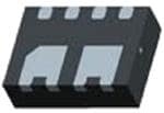
ICGOO电子元器件商城为您提供FAN5602MP5X由Fairchild Semiconductor设计生产,在icgoo商城现货销售,并且可以通过原厂、代理商等渠道进行代购。 FAN5602MP5X价格参考¥6.17-¥6.17。Fairchild SemiconductorFAN5602MP5X封装/规格:PMIC - 稳压器 - DC DC 开关稳压器, 固定 充电泵 开关稳压器 IC 正 5V 1 输出 200mA 8-WDFN 裸露焊盘。您可以下载FAN5602MP5X参考资料、Datasheet数据手册功能说明书,资料中有FAN5602MP5X 详细功能的应用电路图电压和使用方法及教程。
FAN5602MP5X 是安森美半导体(ON Semiconductor)推出的一款高效、同步整流的 DC-DC 降压型开关稳压器,广泛应用于对效率和空间有较高要求的电子设备中。

该器件主要应用于以下场景:

1. 笔记本电脑与超极本:用于为处理器、内存及外围电路提供高效稳定的电源,尤其适用于电池供电系统,有助于延长续航时间。

2. 平板电脑与便携式设备:其高效率和小封装特性适合空间受限的便携设备,降低功耗并减少发热。

3. 通信设备与网络设备:如路由器、交换机等,用于为内部逻辑电路或处理器提供稳定电压。

4. 工业控制系统:适用于工业自动化设备中的电源管理模块,支持宽输入电压范围,适应复杂工业环境。

5. 消费类电子产品:如智能电视、机顶盒、游戏设备等,提供高效电源转换,提升整体能效。

FAN5602MP5X 采用同步整流技术,效率高,静态电流低,具备过流、过温保护功能,增强了系统稳定性与安全性,是一款性能稳定、应用广泛的电源管理IC。
| 参数 | 数值 |
| 产品目录 | 集成电路 (IC)半导体 |
| 描述 | IC REG MULTI CONFIG 5V 0.2A 8MLP稳压器—开关式稳压器 Reg Step-Down Charge Pump DC/DC Converter |
| 产品分类 | |
| 品牌 | Fairchild Semiconductor |
| 产品手册 | |
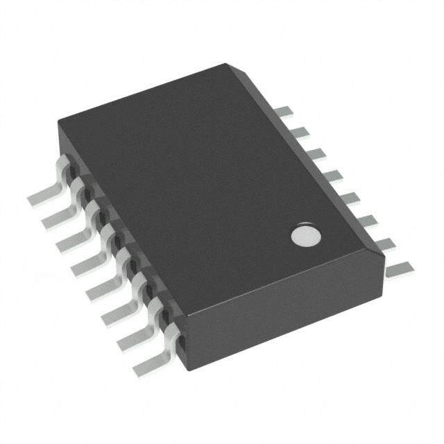
| 产品图片 |
|
| rohs | 符合RoHS无铅 / 符合限制有害物质指令(RoHS)规范要求 |
| 产品系列 | 电源管理 IC,稳压器—开关式稳压器,Fairchild Semiconductor FAN5602MP5X- |
| 数据手册 | |
| 产品型号 | FAN5602MP5X |
| PWM类型 | - |
| 产品种类 | 稳压器—开关式稳压器 |
| 供应商器件封装 | 8-MLP(3x3) |
| 其它名称 | FAN5602MP5XDKR |
| 包装 | Digi-Reel® |
| 单位重量 | 129 mg |
| 同步整流器 | 无 |
| 商标 | Fairchild Semiconductor |
| 安装类型 | 表面贴装 |
| 安装风格 | SMD/SMT |
| 宽度 | 3 mm |
| 封装 | Reel |
| 封装/外壳 | 8-WDFN 裸露焊盘 |
| 封装/箱体 | MLP-8 |
| 工作温度 | -40°C ~ 85°C |
| 工厂包装数量 | 3000 |
| 开关频率 | 1 MHz |
| 最大工作温度 | + 85 C |
| 最大输入电压 | 5.5 V |
| 最小工作温度 | - 40 C |
| 标准包装 | 1 |
| 电压-输入 | 1.8 V ~ 5.5 V |
| 电压-输出 | 5V |
| 电流-输出 | 200mA |
| 类型 | Charge Pump |
| 系列 | FAN5602 |
| 输出数 | 1 |
| 输出电压 | 5 V |
| 输出电流 | 100 mA |
| 输出类型 | 固定 |
| 频率-开关 | 1MHz |


- 商务部:美国ITC正式对集成电路等产品启动337调查
- 曝三星4nm工艺存在良率问题 高通将骁龙8 Gen1或转产台积电
- 太阳诱电将投资9.5亿元在常州建新厂生产MLCC 预计2023年完工
- 英特尔发布欧洲新工厂建设计划 深化IDM 2.0 战略
- 台积电先进制程称霸业界 有大客户加持明年业绩稳了
- 达到5530亿美元!SIA预计今年全球半导体销售额将创下新高
- 英特尔拟将自动驾驶子公司Mobileye上市 估值或超500亿美元
- 三星加码芯片和SET,合并消费电子和移动部门,撤换高东真等 CEO
- 三星电子宣布重大人事变动 还合并消费电子和移动部门
- 海关总署:前11个月进口集成电路产品价值2.52万亿元 增长14.8%


PDF Datasheet 数据手册内容提取
Is Now Part of To learn more about ON Semiconductor, please visit our website at www.onsemi.com Please note: As part of the Fairchild Semiconductor integration, some of the Fairchild orderable part numbers will need to change in order to meet ON Semiconductor’s system requirements. Since the ON Semiconductor product management systems do not have the ability to manage part nomenclature that utilizes an underscore (_), the underscore (_) in the Fairchild part numbers will be changed to a dash (-). This document may contain device numbers with an underscore (_). Please check the ON Semiconductor website to verify the updated device numbers. The most current and up-to-date ordering information can be found at www.onsemi.com. Please email any questions regarding the system integration to Fairchild_questions@onsemi.com. ON Semiconductor and the ON Semiconductor logo are trademarks of Semiconductor Components Industries, LLC dba ON Semiconductor or its subsidiaries in the United States and/or other countries. ON Semiconductor owns the rights to a number of patents, trademarks, copyrights, trade secrets, and other intellectual property. A listing of ON Semiconductor’s product/patent coverage may be accessed at www.onsemi.com/site/pdf/Patent-Marking.pdf. ON Semiconductor reserves the right to make changes without further notice to any products herein. ON Semiconductor makes no warranty, representation or guarantee regarding the suitability of its products for any particular purpose, nor does ON Semiconductor assume any liability arising out of the application or use of any product or circuit, and specifically disclaims any and all liability, including without limitation special, consequential or incidental damages. Buyer is responsible for its products and applications using ON Semiconductor products, including compliance with all laws, regulations and safety requirements or standards, regardless of any support or applications information provided by ON Semiconductor. “Typical” parameters which may be provided in ON Semiconductor data sheets and/or specifications can and do vary in different applications and actual performance may vary over time. All operating parameters, including “Typicals” must be validated for each customer application by customer’s technical experts. ON Semiconductor does not convey any license under its patent rights nor the rights of others. ON Semiconductor products are not designed, intended, or authorized for use as a critical component in life support systems or any FDA Class 3 medical devices or medical devices with a same or similar classification in a foreign jurisdiction or any devices intended for implantation in the human body. Should Buyer purchase or use ON Semiconductor products for any such unintended or unauthorized application, Buyer shall indemnify and hold ON Semiconductor and its officers, employees, subsidiaries, affiliates, and distributors harmless against all claims, costs, damages, and expenses, and reasonable attorney fees arising out of, directly or indirectly, any claim of personal injury or death associated with such unintended or unauthorized use, even if such claim alleges that ON Semiconductor was negligent regarding the design or manufacture of the part. ON Semiconductor is an Equal Opportunity/Affirmative Action Employer. This literature is subject to all applicable copyright laws and is not for resale in any manner.
F A N 5 6 August 2009 0 2 — U FAN5602 — Universal (Step-Up/Step-Down) Charge n i v e Pump Regulated DC/DC Converter r s a l ( Features Description S t e ■Low-Noise, Constant-Frequency Operation at Heavy Load The FAN5602 is a universal switched capacitor DC/DC p - ■High-Efficiency, Pulse-Skip (PFM) Operation at Light Load converter capable of step-up or step-down operation. U ■Switch Configurations (1:3, 1:2, 2:3, 1:1, 3:2, 2:1, 3:1) Due to its unique adaptive fractional switching topology, p/ ■92% Peak Efficiency the device achieves high efficiency over a wider input/ St ■Input Voltage Range: 2.7V to 5.5V output voltage range than any of its predecessors. The ep ■Output Current: 4.5V, 100mA at V = 3.6V FAN5602 utilizes resistance-modulated loop control, -D ■±3% Output Voltage Accuracy IN which produces lower switching noise than other topolo- o gies. Depending upon actual load conditions, the device w ■ICC < 1µA in Shutdown Mode automatically switches between constant-frequency and n ■1MHz Operating Frequency pulse-skipping modes of operation to extend battery life. ) C ■Shutdown Isolates Output from Input h ■Soft-Start Limits Inrush Current at Startup The FAN5602 produces a fixed regulated output within ar ■Short-Circuit and Over-Temperature Protection the range of 2.7V to 5.5V from any type of voltage ge source. High efficiency is achieved under various input/ ■Minimum External Component Count P output voltage conditions because an internal logic circuit ■No Inductors u automatically reconfigures the system to the best possi- m ble topology. Only two 1µF bucket capacitors and one p Applications 10µF output capacitor are needed. During power on, R ■Cell Phones soft-start circuitry prevents excessive current drawn from eg ■Handheld Computers the supply. The device is protected against short-circuit u l ■Portable RF Communication Equipment and over-temperature conditions. a t ■Core Supply to Low-Power Processors The FAN5602 is available with 4.5V and 5.0V output volt- ed ■Low-Voltage DC Bus ages in a 3x3mm 8-lead MLP package. D ■DSP Supplies C / D C Ordering Information C o Part Number Package Eco Status Output Voltage, NVOM n v FAM6502MP45X 3x3mm 8-Lead MLP Green 4.5V e r t FAN5602MP5X 3x3mm 8-Lead MLP Green 5.0V e r Note: 1. Reference MLP08D Option B ONLY. 2. For Fairchild’s definition of “green” Eco Status, please visit: http://www.fairchildsemi.com/company/green/rohs_green.html. Application Diagram Input 2.7V to 5.5V V IN ENABLE 1 8 CIN C2+ 2 6 VOUT CB FAN5602 7 C1+ COUT 3 C2- 4 5 GND C1- Figure 1. Typical Application Diagram © 2005 Fairchild Semiconductor Corporation www.fairchildsemi.com FAN5602 Rev. 1.5.3
F A Block Diagram N 5 6 0 ENABLE VIN C1- C1+ 2 — U BAND GAP n VOUT iv e r s FB a l SOFT-START ERROR ( BG AMP S EN t e p CURRENT S -U SENSE oad WI C2+ p Light load vy L T /S FB EN Hea CH tep BG PFM A -Do R w R n REF A C DRIVER Y ) VIN MODE OGI C2- Ch L L a 150mV TRO rg N e VOUT SC CO P u m 1.6V p R VIN UVLO OSCILLATOR GND e g VIN VOUT ul a t e d D C / Figure 2. Block Diagram D C C o n v e r t e r © 2005 Fairchild Semiconductor Corporation www.fairchildsemi.com FAN5602 Rev. 1.5.3 2
F A Pin Assignments N 5 6 0 2 — U VIN 1 8 ENABLE n C2+ 2 7 C1+ iv e C2- 3 6 VOUT rs GND 4 5 C1- a l ( S 3x3mm 8-Lead MLP t e p - U Figure 3. Pin Assignments p / S Pin Descriptions t e p - Pin # Name Description D o 1 V Supply Voltage Input. w IN n 2 C2+ Bucket Capacitor2. Positive Connection. ) C 3 C2- Bucket Capacitor2. Negative Connection. h a 4 GND Ground r g 5 C1- Bucket Capacitor1. Negative Connection. e P 6 VOUT Regulated Output Voltage. Bypass this pin with 10μF ceramic low-ESR capacitor. u m 7 C1+ Bucket Capacitor1. Positive Connection. p Enable Input. Logic high enables the chip and logic low disables the chip, reducing the R 8 ENABLE supply current to less than 1µA. Do not float this pin. e g u l a t e d D C / D C C o n v e r t e r © 2005 Fairchild Semiconductor Corporation www.fairchildsemi.com FAN5602 Rev. 1.5.3 3
F A Absolute Maximum Ratings N 5 Stresses exceeding the absolute maximum ratings may damage the device. The device may not function or be opera- 6 0 ble above the recommended operating conditions and stressing the parts to these levels is not recommended. In addi- 2 tion, extended exposure to stresses above the recommended operating conditions may affect device reliability. The — absolute maximum ratings are stress ratings only. U n Symbol Parameter Min. Max. Unit i v e VIN VIN, VOUT, ENABLE, Voltage to GND -3.0 6.0 V rs Voltage at C1+,C1-,C2+, and C2-to GND -3.0 V +0.3 V a IN l ( P Power Dissipation Internally Limited S D t e T Lead Soldering Temperature (10 seconds) 300 C° L p - T Junction Temperature 150 C° U J p TSTG Storage Temperature -55 150 C° /S t Human Body Model (HBM) 2 kV e ESD p Charged Device Model (CDM) 2 kV - D Note: o w 2. Using Mil Std. 883E, method 3015.7 (Human Body Model) and EIAJ/JESD22C101-A (Charged Device Model). n ) C h a r g e P Recommended Operating Conditions u m The Recommended Operating Conditions table defines the conditions for actual device operation. Recommended p operating conditions are specified to ensure optimal performance to the datasheet specifications. Fairchild does not R recommend exceeding them or designing to Absolute Maximum Ratings. e g u Symbol Parameter Condition Min. Typ. Max. Unit l a t V Input Voltage 1.8 5.5 V e IN d V < 2V 30 D IN IL Load Current mA C 4.5 & 5.5,VIN = 3.6V 100 /D T Ambient Temperature -40 +85 C° C A C Note: o 3. Refer to Figure 9 in Typical Performance Characteristics. n v e r t e r © 2005 Fairchild Semiconductor Corporation www.fairchildsemi.com FAN5602 Rev. 1.5.3 4
F A DC Electrical Characteristics N 5 6 VIN = 2.7V to 5.5V, C1 = C2 = 1µF, CIN = COUT = 10µF, ENABLE = VIN, TA = -40°C to +85°C unless otherwise noted. 0 Typical values are at T = 25°C. 2 A — Symbol Parameter Condition Min. Typ. Max. Unit U Input Under-Voltage n V 1.5 1.7 2.2 v i UVLO Lockout v e VOUT Output Voltage 0VmINA ≥ <0 .I75 x V <N1O0M0,m A 0.97 x VNOM VNOM 1.03 x VNOM V rsa LOAD l ( V ≥ 1.1 x V , S IQ Quiescent Current IIN = 0mANOM 170 300 µA te LOAD p Off Mode Supply Current ENABLE = GND 0.1 1.0 µA -U p Output Short-Circuit V < 150mV 200 mA OUT / S V = 0.85 x V t IN NOM, 4.5, 5.0V 80 e I = 30mA p LOAD Efficiency % - D V = 1.1 x V IN NOM, 4.5, 5.0V 92 o ILOAD = 30mA w n fOSC Oscillator Frequency TA = 25°C 0.7 1.0 1.3 MHz ) C Thermal Shutdown T 145 °C h SD Threshold a r g Thermal Shutdown T 15 °C e SDHYS Threshold Hysteresis P u V ENABLE Logic Input High 1.5 V m IH Voltage p ENABLE Logic Input Low R VIL Voltage 0.5 V eg u ENABLE Logic Input Bias l I ENABLE =V or GND -1 1 µA a EN Current IN t e d V = 0.9 x V , I = tON VOUT Turn-On Time 0mINA,10% to N90O%M LOAD 0.5 ms D C VOUT Ripple VIN = 2.5V, ILOAD = 200mA 10 mVpp /D C C o n v e r t e r © 2005 Fairchild Semiconductor Corporation www.fairchildsemi.com FAN5602 Rev. 1.5.3 5
F A Typical Performance Characteristics N 5 6 TA = 25°C, VOUT = 4.5V unless otherwise noted. 0 2 — 180 80 U n 160 70 iv 140 e uiescent Current (µA) 110246800000 hutdown Current (nA) 2345600000 rsal (Step-Up Q 20 S 10 /S t e 0 0 p 1.5 2.5 3.5 4.5 5.5 1 2 3 4 5 6 - D Input Voltage (V) Input Voltage (V) o Figure 4. Quiescent Current vs. Input Voltage Figure 5. Shutdown Current vs. Input Voltage w n ) C 4.55 h 100 a r 4.50 90 ge ILOAD = 100mA 80 P put Voltage (V) 44..4405 VOUT = 4.5V Efficiency 567000 ump Re Out 4.35 40 LLooaadd CCuurrrreenntt == 1500mmAA gu 30 LLooaadd CCuurrrreenntt == 110500mmAA la t 4.30 20 e 2.0 2.5 3.0 3.5 4.0 4.5 5.0 5.5 6.0 d 2.500 3.000 3.500 4.000 4.500 5.000 5.500 Input Voltage (V) Input Voltage D C Figure 6. Line Regulation Figure 7. Efficiency vs. Input Voltage / D C C o 4.6 700.0 n v 4.5 600.0 e e (V) 4.4 VIN = 3.6V mA) 500.0 DDVVOOUUTT << 130%% rter ut Voltag 4.3 Current ( 340000..00 Outp 4.2 oad 200.0 L 4.1 100.0 4.0 0.0 1 50 100 150 200 250 300 350 2 2.5 3 3.5 4 4.5 5 Load Currrent (mA) Input Voltage (V) Figure 8. Load Regulation Figure 9. Output Current Capacity vs. Input Voltage © 2005 Fairchild Semiconductor Corporation www.fairchildsemi.com FAN5602 Rev. 1.5.3 6
F A Typical Performance Characteristics N (Continued) 5 6 0 TA = 25°C and VOUT = 4.5V unless otherwise noted. 2 — U 5 4.5 n Load Current = 10mA iv 4.5 e r ut Voltage (V) 3.54 ut Voltage (V) 44.4.45 sal (Step Outp 3 LLooaadd CCuurrrreenntt == 1500mmAA Outp 4.35 -U 2.5 Load Current = 100mA p Load Current = 150mA / S Load Current = 200mA 2 4.3 te 2 3 4 5 6 -60 -40 -20 0 20 40 60 80 100 120 140 p - Input Voltage (V) Ambient Temperature (C) D o Figure 10. Output Voltage vs. Input Voltage Figure 11. Output Voltage vs. Ambient Temperature w n ) C h a r g 80 1.4 e P 1.3 u m 75 p Efficiency (%) 70 VIN = 3.6V Enable (V) 11..112 Regulat 65 e d 0.9 D C 60 0.8 / 0 50 100 150 200 250 300 2 2.5 3 3.5 4 4.5 5 5.5 6 D C Figure 12. Peak Efficiency vs. Load Current Figure 13. Enable Threshold vs. Input Voltage C o n v e r t 5.5 e Mode 1 r 5 V) d ( 4.5 ol sh Mode 2 hre 4 T ge 3.5 n a h C 3 e Mode 3 d Mo 2.5 Mode 4 2 0 50 100 150 200 Load Current (mA) Figure 14. Mode Change Threshold and Hysteresis © 2005 Fairchild Semiconductor Corporation www.fairchildsemi.com FAN5602 Rev. 1.5.3 7
F A Typical Performance Characteristics N (Continued) 5 6 0 TA = 25°C, CIN = COUT = 10µF, CB = 1µF, VOUT = 4.5V unless otherwise noted. 2 — U n IOUT = 200mA IOUT = 200mA i VIN = 2.5V VIN = 3.6V ve r s Output Ripple(20 mV/div) Output Ripple(20 mV/div) al (Step - U p / S t e p - Time (100 µs/div) Time (100 µs/div) D o Figure 15. Output Ripple Figure 16. Output Ripple w n ) C h a r g IVOINU T= = 4 .220V0mA IVOINU T= = 2 .350V0mA e Pum Output Ripple(20 mV/div) Output Ripple (20 mV/div) p Regul a t e d D C / D Time (100 µs/div) Time (100 µs/div) C C Figure 17. Output Ripple Figure 18. Output Ripple o n v e r t e r IOUT= 300mA IOUT = 300mA VIN = 3.6V VIN = 4.2V Output Ripple(20 mV/div) Output Ripple(20 mV/div) Time (100 µs/div) Time (100 µs/div) Figure 19. Output Ripple Figure 20. Output Ripple © 2005 Fairchild Semiconductor Corporation www.fairchildsemi.com FAN5602 Rev. 1.5.3 8
F A Functional Description N 5 6 FAN5602 is a high-efficiency, low-noise switched capaci- input is connected to the bottom the capacitors so that 0 tor DC/DC converter capable of step-up and step-down the top of the capacitors is boosted to a voltage that 2 operations. It has seven built-in switch configurations. equals V /2 + V , i.e., 3/2 x V . By connecting the top — IN IN IN Based on the ratio of the input voltage to the output volt- of the capacitors to the output, one can ideally charge U age, the FAN5602 automatically reconfigures the switch the output to 3/2 x V . If 3/2 x V is higher than the n IN IN i to achieve the highest efficiency. The regulation of the needed V , the linear regulation loop adjusts the on- v OUT e output is achieved by a linear regulation loop, which resistance to drop some voltage. Boosting the voltage of r s modulates the on-resistance of the power transistors so the top of the capacitors to 3/2 x VIN by connecting VIN a that the amount of charge transferred from the input to the bottom of the capacitors, boosts the power efficiency l ( S the flying capacitor at each clock cycle is controlled and 3/2 times. In 2:3 mode, the ideal power efficiency is t is equal to the charge needed by the load. The current V /1.5 x V . For example, if V = 2V, V = 2 x V e OUT IN IN OUT IN p spike is reduced to minimum. At light load, the FAN5602 = 4V, the ideal power efficiency is 100%. - U automatically switches to Pulse Frequency Modulation p When 2 x V > V > 1.5 x V , the 1:2 mode (step-up) (PFM) mode to save power. The regulation at PFM mode IN OUT IN /S shown in Figure 23 is used. Both in the charging phase is achieved by skipping pulses. te and in pumping phase, two flying capacitors are placed p Linear Regulation Loop in parallel. In charging phase, the capacitors are charged - D to the input voltage. In the pumping phase, the input volt- o The FAN5602 operates at constant frequency at load age is placed to the bottom of the capacitors. The top of w higher than 10mA. The linear regulation loop consisting n the capacitors is boosted to 2 x V . By connecting the of power transistors, feedback (resistor divider), and IN ) top of the capacitors to the output, one can ideally C error amplifier is used to realize the regulation of the out- charge the output to 2 x V . Boosting the voltage on the h put voltage and to reduce the current spike. The error IN a top of the capacitors to 2V boosts the power efficiency r amplifier takes feedback and reference as inputs and IN g generates the error voltage signal. The error voltage sig- 2 times. In 1:2 mode, the ideal power efficiency is VOUT/2 e x V . For example, V = 2V, V = 2 x V = 4V, the P nal is then used as the gate voltage of the power transis- IN IN OUT IN ideal power efficiency is 100%. u tor and modulates the on-resistance of the power m transistor and, therefore, the charge transferred from the When 3 x V > V > 2 x V , the 1:3 mode (step-up) p IN OUT IN input to the output is controlled and the regulation of the shown in Figure 24 is used. In charging phase, two flying R e output is realized. Since the charge transfer is controlled, capacitors are placed in parallel and each is charged to g the FAN5602 has a small ESR spike. V . In the pumping phase, the two flying capacitors are u IN l placed in series and the input is connected to the bottom a Switch Array t of the series connected capacitors. The top of the series e d Switch Configurations connected capacitors is boosted to 3 x VIN. The ideal D The FAN5602 has seven built-in switch configurations, power efficiency is boosted 3 times and is equal to VOUT/ C including 1:1, 3:2, 2:1 and 3:1 for step-down and 2:3, 1:2 3VIN. For example, VIN = 1V, VOUT = 3 x VIN = 3V, the /D and 1:3 for step-up. ideal power efficiency is 100%. By connecting the output C to the top of the series connected capacitors, one can C When 1.5 x V > V > V , the 1:1 mode shown in OUT IN OUT charge the output to 3 x V . o Figure 21 is used. In this mode, the internal oscillator is IN n v turned off. The power transistors connecting the input The internal logic in the FAN5602 monitors the input and e and the output become pass transistors and their gate the output compares them, and automatically selects the r t e voltages are controlled by the linear regulation loop, the switch configuration to achieve the highest efficiency. r rest of power transistors are turned off. In this mode, the The step-down modes 3:2, 2:1, and 3:1 can be under- FAN5602 operates exactly like a low dropout (LDO) regu- stood by reversing the function of V and V in the lator and the ripple of the output is in the micro-volt range. IN OUT above discussion. When 1.5 x V > V > V , the 2:3 mode (step-up) IN OUT IN The built-in modes improve power efficiency and extend shown in Figure 22 is used. In the charging phase, two the battery life. For example, if V = 5V, mode 1:2 flying capacitors are placed in series and each capacitor OUT needs a minimum V = 2.5V. By built-in 1:3 mode, the is charged to a half of the input voltage. In pumping IN minimum battery voltage is extended to 1.7V. phase, the flying capacitors are placed in parallel. The © 2005 Fairchild Semiconductor Corporation www.fairchildsemi.com FAN5602 Rev. 1.5.3 9
F A Switch Array Modes N 5 6 0 TOP TOP 2 — C1+ S1A S1A C1+ U S1A C1+ n i S2A v MID C 1 C 2 er S2A C 1 S3A S3B sa l ( MID C1- S5 S4B C1- S C1- t e p GND GND - U p Figure 21. Mode 1 (1:1) Figure 22. Mode 2 (2:3 or 3:2) All Switches Set for / S Phase 1 and Reverse State for Phase 2 t e TOP TOP p - D o C1+ S1A S1B C2+ C1+ S1A C2+ w n S2A S2B ) S2A S2B C 1 MID C 2 C C 1 MID C 2 S3B ha S3A S3B C1- S4A S5 S4B C2- rge C1- S4A S4B C2- P u m GND p Figure 24. Mode 4 (1:3 or 3:1) All Switches Set for R Figure 23. Mode 3 (1:2 or 2:1) All Switches Set for Phase 1 and Reverse State for Phase 2 e Phase 1 and Reverse State for Phase 2 g u Light-Load Operation la t e The power transistors used in the charge pump are very Short Circuit d large in size. The dynamic loss from the switching the D When the output voltage is lower than 150mV, the power transistors is not small and increases its propor- C FAN5602 enters short-circuit condition. In this condition, / tion of the total power consumption as the load gets light. D all power transistors are turned off. A small transistor C To save power, the FAN5602 switches, when the load is shorting the input and the output turns on and charges less than 10mA, from constant frequency to pulse-skip- C ping mode (PFM) for modes 2:3(3:2), 1:2(2:1) and t<h1e5 0omutVp.u tS. iTnhceis tthraisn striastnosri ssttoary sis ovne rays slomnagl l,a sth teh ec uVrrOeUnTt on 1:3(3:1), except mode 1:1. In PFM mode, the linear loop v from the input to the output is limited. Once the short at e is disabled and the error amplifier is turned off. A PFM r the output is eliminated, this transistor is large enough to t comparator is used to setup an upper threshold and a e charge the output higher than 150mV and the FAN5602 r lower threshold for the output. When the output is lower enters soft-start period. than the lower threshold, the oscillator is turned on and the charge pump starts working and keeps delivering Soft Start charges from the input to the output until the output is The FAN5602 uses a constant current, charging a low- higher than the upper threshold. The oscillator shuts off pass filter to generate a ramp. The ramp is used as refer- power transistors and delivers the charge to the output ence voltage during the startup. Since the ramp starts at from the output capacitor. PFM operation is not used for zero and goes up slowly, the output follows the ramp and Mode 1:1, even if at light load. Mode 1:1 is designed as inrush current is restricted. When the ramp is higher than an LDO with the oscillator off. The power transistors at bandgap voltage, the bandgap voltage supersedes ramp LDO mode are not switching and therefore do not have as reference and the soft start is over. The soft start the dynamic loss. takes about 500µs. Switching from linear operation to PFM mode Thermal Shutdown (I <10mA) and from PFM to linear mode LOAD (I >10mA) is automatic, based on the load current, The FAN5602 goes to thermal shutdown if the junction LOAD which is monitored all the time. temperature is over 150°C with 15°C hysteresis. © 2005 Fairchild Semiconductor Corporation www.fairchildsemi.com FAN5602 Rev. 1.5.3 10
F A Application Information N 5 6 Using the FAN5602 to Drive LCD Backlighting 0 2 The FAN5602 4.5V option is ideal for driving the back- problem. The backlight and flash LEDs still produce opti- — lighting and flash LEDs for portable devices. One mal brightness at the reduced regulation. When building U FAN5602 device can supply the roughly 150mA needed this circuit, use ceramic capacitors with low ESR. All n to power both the backlight and the flash LEDs. Even capacitors should be placed as close as possible to the iv though drawing this much current from the FAN5602 FAN5602 in the PCB layout. e r drives the part out of the 3% output regulation, it is not a s a l ( FOL216CIW FOL625CIW S VIN VOUT te p 3B.2A TtoT E4R.2YV 10µF FAN5602 10µF -U p / S t 50 50 50 50 20 e p - D 1µF 1µF o w BACKLIGHT FLASH n ) C h Figure 25. Circuit for Backlighting / Flash Application a r g e P u m p R e g u l a t e d D C / D C C o n v e r t e r © 2005 Fairchild Semiconductor Corporation www.fairchildsemi.com FAN5602 Rev. 1.5.3 11
F A Package Dimensions N 5 6 . 0 2 — U n i v e r s a l ( S t e p - U p / S t e p - D o w n ) C h a r g e P u m p R e g u l a t e d D C / D C C o n v e r t e r Figure 26. 8-Lead, 3x3mm, Molded Leadless Package (MLP), .8mm Thick Package drawings are provided as a service to customers considering Fairchild components. Drawings may change in any manner without notice. Please note the revision and/or date on the drawing and contact a Fairchild Semiconductor representative to verify or obtain the most recent revision. Package specifications do not expand the terms of Fairchild’s worldwide terms and conditions, specifically the warranty therein, which covers Fairchild products. Always visit Fairchild Semiconductor’s online packaging area for the most recent package drawings: http://www.fairchildsemi.com/packaging/. © 2005 Fairchild Semiconductor Corporation www.fairchildsemi.com FAN5602 Rev. 1.5.3 12
F A N 5 6 0 2 — U n i v e r s a l ( S t e p - U p / S t e p - D o w n ) C h a r g e P u m p R e g u l a t e d D C / D C C o n v e r t e r © 2005 Fairchild Semiconductor Corporation www.fairchildsemi.com FAN5602 Rev. 1.5.3 13
ON Semiconductor and are trademarks of Semiconductor Components Industries, LLC dba ON Semiconductor or its subsidiaries in the United States and/or other countries. ON Semiconductor owns the rights to a number of patents, trademarks, copyrights, trade secrets, and other intellectual property. A listing of ON Semiconductor’s product/patent coverage may be accessed at www.onsemi.com/site/pdf/Patent−Marking.pdf. ON Semiconductor reserves the right to make changes without further notice to any products herein. ON Semiconductor makes no warranty, representation or guarantee regarding the suitability of its products for any particular purpose, nor does ON Semiconductor assume any liability arising out of the application or use of any product or circuit, and specifically disclaims any and all liability, including without limitation special, consequential or incidental damages. Buyer is responsible for its products and applications using ON Semiconductor products, including compliance with all laws, regulations and safety requirements or standards, regardless of any support or applications information provided by ON Semiconductor. “Typical” parameters which may be provided in ON Semiconductor data sheets and/or specifications can and do vary in different applications and actual performance may vary over time. All operating parameters, including “Typicals” must be validated for each customer application by customer’s technical experts. ON Semiconductor does not convey any license under its patent rights nor the rights of others. ON Semiconductor products are not designed, intended, or authorized for use as a critical component in life support systems or any FDA Class 3 medical devices or medical devices with a same or similar classification in a foreign jurisdiction or any devices intended for implantation in the human body. Should Buyer purchase or use ON Semiconductor products for any such unintended or unauthorized application, Buyer shall indemnify and hold ON Semiconductor and its officers, employees, subsidiaries, affiliates, and distributors harmless against all claims, costs, damages, and expenses, and reasonable attorney fees arising out of, directly or indirectly, any claim of personal injury or death associated with such unintended or unauthorized use, even if such claim alleges that ON Semiconductor was negligent regarding the design or manufacture of the part. ON Semiconductor is an Equal Opportunity/Affirmative Action Employer. This literature is subject to all applicable copyright laws and is not for resale in any manner. PUBLICATION ORDERING INFORMATION LITERATURE FULFILLMENT: N. American Technical Support: 800−282−9855 Toll Free ON Semiconductor Website: www.onsemi.com Literature Distribution Center for ON Semiconductor USA/Canada 19521 E. 32nd Pkwy, Aurora, Colorado 80011 USA Europe, Middle East and Africa Technical Support: Order Literature: http://www.onsemi.com/orderlit Phone: 303−675−2175 or 800−344−3860 Toll Free USA/Canada Phone: 421 33 790 2910 Fax: 303−675−2176 or 800−344−3867 Toll Free USA/Canada Japan Customer Focus Center For additional information, please contact your local Email: orderlit@onsemi.com Phone: 81−3−5817−1050 Sales Representative © Semiconductor Components Industries, LLC www.onsemi.com www.onsemi.com 1
Mouser Electronics Authorized Distributor Click to View Pricing, Inventory, Delivery & Lifecycle Information: O N Semiconductor: FAN5602MP45X FAN5602MP5X