ICGOO在线商城 > 集成电路(IC) > PMIC - 稳压器 - DC DC 开关稳压器 > TPS54295PWPR
 Datasheet下载
- 型号: TPS54295PWPR
- 制造商: Texas Instruments
- 库位|库存: xxxx|xxxx
- 要求:
| 数量阶梯 | 香港交货 | 国内含税 |
| +xxxx | $xxxx | ¥xxxx |
查看当月历史价格
查看今年历史价格
TPS54295PWPR产品简介:
ICGOO电子元器件商城为您提供TPS54295PWPR由Texas Instruments设计生产,在icgoo商城现货销售,并且可以通过原厂、代理商等渠道进行代购。 TPS54295PWPR价格参考¥6.94-¥14.09。Texas InstrumentsTPS54295PWPR封装/规格:PMIC - 稳压器 - DC DC 开关稳压器, 可调式 降压 开关稳压器 IC 正 0.76V 2 输出 2A 16-TSSOP(0.173",4.40mm 宽)裸露焊盘。您可以下载TPS54295PWPR参考资料、Datasheet数据手册功能说明书,资料中有TPS54295PWPR 详细功能的应用电路图电压和使用方法及教程。
TPS54295PWPR 是 Texas Instruments(德州仪器)推出的一款高效同步降压开关稳压器,属于 PMIC(电源管理集成电路)中的 DC-DC 开关稳压器类别。该器件适用于多种需要高效、低功耗和高精度电压调节的应用场景,以下是其主要应用场景:

1. 工业设备
   - 用于工业自动化设备、可编程逻辑控制器(PLC)、数据采集系统等,为微控制器、传感器和其他关键组件提供稳定电源。
   - 在工业通信模块中,为以太网供电(PoE)或其他通信接口供电。

2. 通信设备
   - 为基站、路由器、交换机等通信设备中的射频(RF)模块、数字信号处理器(DSP)和现场可编程门阵列(FPGA)供电。
   - 提供高效的电源转换,支持高带宽数据传输和处理需求。

3. 消费电子
   - 用于便携式设备(如平板电脑、智能音箱、游戏机等),提供高效电源管理以延长电池寿命。
   - 为音频放大器、显示屏驱动器等外围设备供电,确保稳定的性能表现。

4. 汽车电子
   - 应用于车载信息娱乐系统、导航系统和高级驾驶辅助系统(ADAS),为摄像头、传感器和处理器供电。
   - 支持宽输入电压范围,适应汽车电池电压波动的环境。

5. 医疗设备
   - 为便携式医疗设备(如血糖仪、心率监测仪)提供低功耗电源解决方案。
   - 在更复杂的医疗设备(如超声波设备、监护仪)中,为高性能处理器和传感器供电。

6. 物联网(IoT)设备
   - 为低功耗 IoT 网关、传感器节点和无线模块供电,支持长时间运行和远程监控。
   - 其高效率和小尺寸设计非常适合空间受限的 IoT 应用。

TPS54295PWPR 的特点包括高效率、低静态电流、快速瞬态响应和集成 MOSFET,使其能够满足现代电子设备对电源管理的严格要求。无论是需要高功率还是低功耗的应用场景,这款稳压器都能提供可靠且高效的电源解决方案。
| 参数 | 数值 |
| 产品目录 | 集成电路 (IC)半导体 |
| 描述 | IC REG BUCK SYNC ADJ 2A 16HTSSOP稳压器—开关式稳压器 4.5-8Vin,Dual 2A Out Sync SD Converter |
| DevelopmentKit | TPS54295EVM-057 |
| 产品分类 | |
| 品牌 | Texas Instruments |
| 产品手册 | |
| 产品图片 |
|
| rohs | 符合RoHS无铅 / 符合限制有害物质指令(RoHS)规范要求 |
| 产品系列 | 电源管理 IC,稳压器—开关式稳压器,Texas Instruments TPS54295PWPRD-CAP2™, Eco-Mode™ |
| 数据手册 | |
| 产品型号 | TPS54295PWPR |
| PWM类型 | 混合物 |
| 产品种类 | 稳压器—开关式稳压器 |
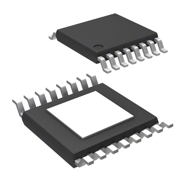
| 供应商器件封装 | 16-HTSSOP |
| 其它名称 | 296-29960-6 |
| 包装 | Digi-Reel® |
| 同步整流器 | 是 |
| 商标 | Texas Instruments |
| 安装类型 | 表面贴装 |
| 安装风格 | SMD/SMT |
| 封装 | Reel |
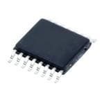
| 封装/外壳 | 16-TSSOP (0.173", 4.40mm 宽)裸焊盘 |
| 封装/箱体 | HTSSOP-16 |
| 工作温度 | -40°C ~ 85°C |
| 工作温度范围 | - 40 C to + 85 C |
| 工厂包装数量 | 2000 |
| 开关频率 | 700 kHz |
| 拓扑结构 | Buck |
| 最大输入电压 | 18 V |
| 最小工作温度 | - 40 C |
| 标准包装 | 1 |
| 电压-输入 | 4.5 V ~ 18 V |
| 电压-输出 | 0.76 V ~ 7 V |
| 电流-输出 | 2A |
| 类型 | 降压(降压) |
| 系列 | TPS54295 |
| 输出数 | 2 |
| 输出电压 | 760 mV to 7 V |
| 输出电流 | 2 A |
| 输出端数量 | 2 Output |
| 输出类型 | 可调式 |
| 配用 | /product-detail/zh/TPS54295EVM-057/296-31189-ND/2797907 |
| 频率-开关 | 700kHz |


- 商务部:美国ITC正式对集成电路等产品启动337调查
- 曝三星4nm工艺存在良率问题 高通将骁龙8 Gen1或转产台积电
- 太阳诱电将投资9.5亿元在常州建新厂生产MLCC 预计2023年完工
- 英特尔发布欧洲新工厂建设计划 深化IDM 2.0 战略
- 台积电先进制程称霸业界 有大客户加持明年业绩稳了
- 达到5530亿美元!SIA预计今年全球半导体销售额将创下新高
- 英特尔拟将自动驾驶子公司Mobileye上市 估值或超500亿美元
- 三星加码芯片和SET,合并消费电子和移动部门,撤换高东真等 CEO
- 三星电子宣布重大人事变动 还合并消费电子和移动部门
- 海关总署:前11个月进口集成电路产品价值2.52万亿元 增长14.8%


PDF Datasheet 数据手册内容提取
Product Sample & Technical Tools & Support & Folder Buy Documents Software Community TPS54295 SLVSB01D–OCTOBER2011–REVISEDAUGUST2016 TPS54295 2-A Dual Channel Synchronous Step-Down Switcher With Integrated FET 1 Features 3 Description • D-CAP2™ControlMode The TPS54295 is a dual, adaptive on-time D-CAP2 1 mode synchronous buck converter. The TPS54295 – FastTransientResponse enables system designers to complete the suite of – NoExternalPartsRequiredForLoop various end-equipment power bus regulators with a Compensation cost effective, low component count, and low standby current solution. The main control loops of the – CompatibleWithCeramicOutputCapacitors TPS54295 use the D-CAP2 mode control which • WideInputVoltageRange:4.5Vto18V provides a very fast transient response with no • OutputVoltageRange:0.76Vto7V externalcompensationcomponents.Theadaptiveon- • HighlyEfficientIntegratedFETsOptimizedfor time control supports seamless transition between LowDutyCycleApplications PWM mode at higher load conditions and Eco-mode operation at light loads. Eco-mode allows the – 150mΩ (High-Side)and100mΩ(Low-Side) TPS54295 to maintain high efficiency during lighter • HighInitialReferenceAccuracy load conditions. The TPS54295 is able to adapt to • Low-Sider LosslessCurrentSensing both low equivalent series resistance (ESR) output DS(ON) capacitors such as POSCAP or SP-CAP, and ultra- • AdjustableSoftStart low ESR ceramic capacitors. The device provides • Non-SinkingPrebiasedSoftStart convenient and efficient operation with input voltages • 700-kHzSwitchingFrequency from4.5Vto18V. • Cycle-by-CycleOvercurrentLimitControl The TPS54295 is available in a 4.4 mm × 5 mm 16- • OCL,OVP,UVP,UVLO,andTSDProtections pin HTSSOP (PWP) package and 4 mm x 4 mm 16- pin VQFN (RSA) package, designed to operate at an • AdaptiveGateDriversWithIntegratedBoost ambienttemperaturerangefrom–40°Cto85°C. PMOSSwitch • OCPConstantDuetoThermallyCompensated DeviceInformation(1) r With4000ppm/℃ DS(ON) PARTNUMBER PACKAGE BODYSIZE(NOM) • 16-PinHTSSOP,16-pinVQFN HTSSOP(16) 5.00mm×4.40mm TPS54295 • Auto-SkipEco-mode™forHighEfficiencyatLight VQFN(16) 4.00mm×4.00mm Load (1) For all available packages, see the orderable addendum at theendofthedatasheet. 2 Applications LoadTransientResponse • Point-of-LoadRegulationinLowPowerSystems forWideRangeofApplications – DigitalTVPowerSupplies V O 2 = 1.5 V (50 mV/div) – NetworkingHomeTerminals – DigitalSetTopBoxes(STB) – DVDPlayersandRecorders – GamingConsolesandOther Iout (1A/div) t - Time - 100ms/div 1 An IMPORTANT NOTICE at the end of this data sheet addresses availability, warranty, changes, use in safety-critical applications, intellectualpropertymattersandotherimportantdisclaimers.PRODUCTIONDATA.
TPS54295 SLVSB01D–OCTOBER2011–REVISEDAUGUST2016 www.ti.com Table of Contents 1 Features.................................................................. 1 8 ApplicationandImplementation........................ 15 2 Applications........................................................... 1 8.1 ApplicationInformation............................................15 3 Description............................................................. 1 8.2 TypicalApplication..................................................15 4 RevisionHistory..................................................... 2 9 PowerSupplyRecommendations...................... 19 5 PinConfigurationandFunctions......................... 4 10 Layout................................................................... 19 6 Specifications......................................................... 5 10.1 LayoutGuidelines.................................................19 6.1 AbsoluteMaximumRatings......................................5 10.2 LayoutExample....................................................20 6.2 ESDRatings..............................................................5 10.3 ThermalConsiderations........................................22 6.3 RecommendedOperatingConditions.......................5 11 DeviceandDocumentationSupport................. 23 6.4 ThermalInformation..................................................6 11.1 DeviceSupport......................................................23 6.5 ElectricalCharacteristics...........................................6 11.2 DocumentationSupport........................................23 6.6 TypicalCharacteristics..............................................8 11.3 ReceivingNotificationofDocumentationUpdates23 7 DetailedDescription............................................ 11 11.4 CommunityResources..........................................23 7.1 Overview.................................................................11 11.5 Trademarks...........................................................23 7.2 FunctionalBlockDiagram.......................................12 11.6 ElectrostaticDischargeCaution............................23 7.3 FeatureDescription.................................................13 11.7 Glossary................................................................23 7.4 DeviceFunctionalModes........................................14 12 Mechanical,Packaging,andOrderable Information........................................................... 23 4 Revision History NOTE:Pagenumbersforpreviousrevisionsmaydifferfrompagenumbersinthecurrentversion. ChangesfromRevisionC(April2013)toRevisionD Page • AddedDeviceInformationtable,Specificationssection,ESDRatingstable,DetailedDescriptionsection,Application andImplementationsection,PowerSupplyRecommendationssection,Layoutsection,DeviceandDocumentation Supportsection,andMechanical,Packaging,andOrderableInformationsection................................................................ 1 • DeletedOrderingInformationtable;seePOAattheendofthedatasheet........................................................................... 1 • DeletedOperatingambienttemperaturefromAbsoluteMaximumRatingstable.................................................................. 5 • DeletedOperatingambienttemperaturefromRecommendedOperatingConditionstable................................................... 5 • ChangedOperatingjunctiontemperaturemaximumvaluefrom150to125inRecommendedOperatingConditionstable 5 ChangesfromRevisionB(December2011)toRevisionC Page • AddedtheRSA-16PinpackagetotheOrderingInformationtable........................................................................................ 1 • ChangedtheDescriptiontexttoincludetheRSApackage................................................................................................... 1 • AddedtheRSA-16Pinpackagepinout................................................................................................................................. 4 • AddedFigure26................................................................................................................................................................... 21 ChangesfromRevisionA(October2011)toRevisionB Page • DeletedMINandMAXvaluesfromV specification........................................................................................................ 6 VREG5 • DeletedLineandLoadregulationspecsfromV specification......................................................................................... 6 REG5 • Added"Ensuredbydesign.Notproductiontested"annotationtospecificationsforMOSFETs,ON-TIMETIMER CONTROl,andSOFTSTART................................................................................................................................................ 6 • DeletedMINandMAXvaluesfromV specification...................................................................................................... 6 UVREG5 • Added"VIN=12V,T =25°C(unlessotherwisenoted)"toTypicalCharacteristicsconditionsstatement.......................... 8 A 2 SubmitDocumentationFeedback Copyright©2011–2016,TexasInstrumentsIncorporated ProductFolderLinks:TPS54295
TPS54295 www.ti.com SLVSB01D–OCTOBER2011–REVISEDAUGUST2016 ChangesfromOriginal(October2011)toRevisionA Page • Addedindicationfornotproductiontestedparameters.......................................................................................................... 6 • AddedOver/UnderVoltageProtectionDescription.............................................................................................................. 14 Copyright©2011–2016,TexasInstrumentsIncorporated SubmitDocumentationFeedback 3 ProductFolderLinks:TPS54295
TPS54295 SLVSB01D–OCTOBER2011–REVISEDAUGUST2016 www.ti.com 5 Pin Configuration and Functions PWPPackage RSAPackage 16-PinHTSSOP 16-PinVQFN TopView TopView 2 D W2 GN N2 S2 VIN1 1 16 VIN2 S P E S VBST1 2 15 VBST2 SW1 3 14 SW2 6 5 4 3 1 1 1 1 VBST2 1 12 VFB2 PGND1 4 13 PGND2 Thermal Pad VIN2 2 11 VREG5 EN1 5 12 EN2 Thermal Pad VIN1 3 10 GND SS1 6 11 SS2 VBST1 4 9 VFB1 VFB1 7 10 VFB2 5 6 7 8 GND 8 9 VREG5 Not to scale 1 1 1 1 W D N S S N E S Not to scale G P PinFunctions PIN I/O DESCRIPTION NAME HTSSOP VQFN EN1 5 7 I Enable.Pullhightoenablethecorresponding(1or2)converter. EN2 12 14 GND 8 10 I/O SignalGND.ConnectsensitiveSSxandVFBxreturnstoGNDatasinglepoint. PGND1 4 6 I/O Groundreturnsforlow-sideMOSFETs.Inputofcurrentcomparator. PGND2 13 15 SS1 6 8 O Soft-startprogrammingpin.ConnectcapacitorfromSSxpintoGNDtoprogramsoft-starttime. SS2 11 13 SW1 3 5 Switchnodeconnectionsforboththehigh-sideNFETsandlow-sideNFETs.Inputofcurrent I/O SW2 14 16 comparator. VBST1 2 14 Supplyinputforhigh-sideNFETgatedrivecircuit.Connecta0.1-µFceramiccapacitorbetween I VBST2 15 1 VBSTxandSWxpins.AninternaldiodeisconnectedbetweenVREG5andVBSTx. VFB1 7 9 I D-CAP2feedbackinputs.Connecttooutputvoltagewithresistordivider. VFB2 10 12 VIN1 1 3 Powerinputsandconnectstobothhigh-sideNFETdrains.SupplyInputfor5.5-Vlinear I VIN2 16 2 regulator. Outputof5.5-Vlinearregulator.BypasstoGNDwithahigh-qualityceramiccapacitorofatleast VREG5 9 11 O 1µF.VREG5isactivewhenVIN1isadded. Thermal Thermalpadofthepackage.Mustbesolderedtogroundtoachieveappropriatedissipation. — — — Pad MustbeconnectedtoGND. 4 SubmitDocumentationFeedback Copyright©2011–2016,TexasInstrumentsIncorporated ProductFolderLinks:TPS54295
TPS54295 www.ti.com SLVSB01D–OCTOBER2011–REVISEDAUGUST2016 6 Specifications 6.1 Absolute Maximum Ratings overoperatingfree-airtemperaturerange(unlessotherwisenoted)(1)(2) MIN MAX UNIT VIN1,VIN2,EN1,EN2 –0.3 20 VBST1,VBST2 –0.3 26 VBST1,VBST2(10-nstransient) –0.3 28 Inputvoltage VBST1–SW1,VBST2–SW2 –0.3 6.5 V VFB1,VFB2 –0.3 6.5 SW1,SW2 –2 20 SW1,SW2(10-nstransient) –3 22 VREG5,SS1,SS2 –0.3 6.5 Outputvoltage V PGND1,PGND2 –0.3 0.3 Junctiontemperature,T –40 150 °C J Storagetemperature,T –55 150 °C stg (1) StressesbeyondthoselistedunderAbsoluteMaximumRatingsmaycausepermanentdamagetothedevice.Thesearestressratings only,whichdonotimplyfunctionaloperationofthedeviceattheseoranyotherconditionsbeyondthoseindicatedunderRecommended OperatingConditions.Exposuretoabsolute-maximum-ratedconditionsforextendedperiodsmayaffectdevicereliability. (2) AllvoltagesarewithrespecttoICGNDterminal. 6.2 ESD Ratings VALUE UNIT Human-bodymodel(HBM),perANSI/ESDA/JEDECJS-001(1) ±2000 V Electrostaticdischarge V (ESD) Charged-devicemodel(CDM),perJEDECspecificationJESD22-C101(2) ±500 (1) JEDECdocumentJEP155statesthat500-VHBMallowssafemanufacturingwithastandardESDcontrolprocess. (2) JEDECdocumentJEP157statesthat250-VCDMallowssafemanufacturingwithastandardESDcontrolprocess. 6.3 Recommended Operating Conditions overoperatingfree-airtemperaturerange(unlessotherwisenoted) MIN MAX UNIT Supplyinputvoltage VIN1,VIN2 4.5 18 V VBST1,VBST2 –0.1 24 VBST1,VBST2(10-nstransient) –0.1 27 VBST1–SW1,VBST2–SW2 –0.1 5.7 Inputvoltage VFB1,VFB2 –0.1 5.7 V EN1,EN2 –0.1 18 SW1,SW2 –1 18 SW1,SW2(10-nstransient) –3 21 VREG5,SS1,SS2 –0.1 5.7 Outputvoltage PGND1,PGND2 –0.1 0.1 V VO1,VO2 0.76 7 T OperatingJunctionTemperature –40 125 °C J Copyright©2011–2016,TexasInstrumentsIncorporated SubmitDocumentationFeedback 5 ProductFolderLinks:TPS54295
TPS54295 SLVSB01D–OCTOBER2011–REVISEDAUGUST2016 www.ti.com 6.4 Thermal Information TPS54295 THERMALMETRIC(1) PWP(HTSSOP) RSA(VQFN) UNIT 16PINS 16PINS R Junction-to-ambientthermalresistance 47.5 34.9 °C/W θJA R Junction-to-case(top)thermalresistance 27.1 40 °C/W θJC(top) R Junction-to-boardthermalresistance 20.8 11.8 °C/W θJB ψ Junction-to-topcharacterizationparameter 1 0.7 °C/W JT ψ Junction-to-boardcharacterizationparameter 20.6 11.3 °C/W JB R Junction-to-case(bottom)thermalresistance 2.7 3.3 °C/W θJC(bot) (1) Formoreinformationabouttraditionalandnewthermalmetrics,seetheSemiconductorandICPackageThermalMetricsapplication report. 6.5 Electrical Characteristics overrecommendedfree-airtemperaturerange,V =12V(unlessotherwisenoted) IN PARAMETER TESTCONDITIONS MIN TYP MAX UNIT SUPPLYCURRENT I VINxsupplycurrent T =25°C,V =V =5V,V =V =0.8V 1300 2000 µA IN A EN1 EN2 VFB1 VFB2 I VINxshutdowncurrent T =25°C,V =V =0V 80 150 µA VINSDN A EN1 EN2 FEEDBACKVOLTAGE V VFBxthresholdvoltage T =25°C,V =3.3V,V =1.5V 758 765 773 mV VFBTHLx A CH1 CH2 TC Temperaturecoefficient Onthebasisof25°C(1) –115 115 ppm/℃ VFBx I VFBxInputCurrent V =0.8V,T =25°C –0.35 0.2 0.35 µA VFBx VFBx A VREG5OUTPUT V VREG5outputvoltage T =25°C,6V<V 1<18V,I =5mA 5.5 V VREG5 A IN VREG5 I Outputcurrent V 1=6V,V =4V,T =25°C(1) 75 mA VREG5 IN VREG5 A MOSFETs r High-sideswitchresistance T =25℃,V –V =5.5V (1) 150 mΩ DS(ON)H A VBSTx SWx r Low-sideswitchresistance T =25℃ (1) 100 mΩ DS(ON)L A ON-TIMETIMERCONTROL T SW1ONtime V =12V,V 1=1.2V 165 ns ON1 SW1 OUT T SW2ONtime V =12V,V 2=1.2V 165 ns ON2 SW2 OUT T SW1minimumOFFtime T =25℃,V =0.7V(1) 220 ns OFF1 A VFB1 T SW2minimumOFFtime T =25℃,V =0.7V(1) 220 ns OFF2 A VFB2 SOFTSTART I SSxchargecurrent V =0.5V,T =25℃ –8.4 –8 –7.6 µA SSC SSx A Onthebasisof25°C(1)(PWP) –4 3 TC I temperaturecoefficient nA/°C ISSC SSC Onthebasisof25°C(1)(RSA) –4 5 I SSxdischargecurrent V =0.5V 3 7 10 mA SSD SSx UVLO VREG5rising 3.83 V VREG5UVLOthreshold V UVREG5 Hysteresis 0.6 LOGICTHRESHOLDS V ENxH-levelthresholdvoltage 2 V ENxH V ENxL-levelthresholdvoltage 0.4 V ENxL R ENxinputresistance V =12V 225 450 900 kΩ ENx_IN ENx CURRENTLIMITS I Currentlimit L =2.2µH(1) 2.7 3.9 4.5 A OCL OUT (1) Ensuredbydesign.Notproductiontested. 6 SubmitDocumentationFeedback Copyright©2011–2016,TexasInstrumentsIncorporated ProductFolderLinks:TPS54295
TPS54295 www.ti.com SLVSB01D–OCTOBER2011–REVISEDAUGUST2016 Electrical Characteristics (continued) overrecommendedfree-airtemperaturerange,V =12V(unlessotherwisenoted) IN PARAMETER TESTCONDITIONS MIN TYP MAX UNIT OUTPUTUNDERVOLTAGEANDOVERVOLTAGEPROTECTION(UVP,OVP) V OutputOVPtripthreshold measuredonVFBx 115% 120% 125% OVP T OutputOVPpropdelay 3 10 µs OVPDEL V OutputUVPtripthreshold measuredonVFBx 63% 68% 73% UVP T OutputUVPdelaytime 1.5 ms UVPDEL T OutputUVPenabledelay UVPenabledelayandsoft-starttime ×1.4 ×1.7 ×2 UVPEN THERMALSHUTDOWN Shutdowntemperature(1) 155 T Thermalshutdownthreshold °C SD Hysteresis(1) 25 Copyright©2011–2016,TexasInstrumentsIncorporated SubmitDocumentationFeedback 7 ProductFolderLinks:TPS54295
TPS54295 SLVSB01D–OCTOBER2011–REVISEDAUGUST2016 www.ti.com 6.6 Typical Characteristics Oneoutputisenabledunlessotherwisenoted.V =V 1orV 2.V =12V,T =25°C(unlessotherwisenoted). I IN IN IN A 200 VIN1 = VIN2 = 12V EN1 = EN2 = ON 180 A 160 m nt - 140 e Curr 120 n w o 100 d ut h 80 S dn - 60 s c vc 40 I 20 0 -50 0 50 100 150 TJ- Junction Temperature - °C Figure1.InputCurrentvsJunctionTemperature Figure2.InputShutdownCurrentvsJunctionTemperature 100 3.4 90 3.38 80 3.36 Am 70 e - V 3.34 VI= 12 V VI= 18 V put Current - 456000 Output Voltag 33..323.823 EN In 30 V- O3.26 VI= 5 V 20 3.24 3.22 10 3.2 0 0 0.2 0.4 0.6 0.8 1 1.2 1.4 1.6 1.8 2 0 5 10 15 20 EN Input Voltage - V IO- Output Current -A VENx=12V VOUT1=3.3V Figure3.ENCurrentvsENVoltage Figure4.OutputVoltagevsOutputCurrent 1.55 3.4 1.54 3.38 1.53 3.36 V- Output Voltage - VO1111....14455.89125 VI= 12 V VVII== 5 1 V8 V V- Output Voltage - VO3333....32233.68243 Io1Io=1 1= A10 mA 1.47 3.24 1.46 3.22 1.45 3.2 0 0.2 0.4 0.6 0.8 1 1.2 1.4 1.6 1.8 2 0 2 4 6 8 10 12 14 16 18 20 IO- Output Current -A VI- Input Voltage - V VOUT2=1.5V VOUT1=3.3V Figure5.OutputVoltagevsOutputCurrent Figure6.OutputVoltagevsInputVoltage 8 SubmitDocumentationFeedback Copyright©2011–2016,TexasInstrumentsIncorporated ProductFolderLinks:TPS54295
TPS54295 www.ti.com SLVSB01D–OCTOBER2011–REVISEDAUGUST2016 Typical Characteristics (continued) Oneoutputisenabledunlessotherwisenoted.V =V 1orV 2.V =12V,T =25°C(unlessotherwisenoted). I IN IN IN A 1.55 100 1.54 90 1.53 Output Voltage - V 111...1455.9125 Io2= 1IAo2= 10 mA Efficiency - % 7800 VI= 5 V VI= 12 V VI= 18 V - 60 O1.48 V 1.47 50 1.46 1.45 40 0 2 4 6 8 10 12 14 16 18 20 0 0.5 1 1.5 2 VI- Input Voltage - V IO- Output Current -A VOUT2=1.5V VOUT1=3.3V Figure7.OutputVoltagevsInputVoltage Figure8.EfficiencyvsOutputCurrent 100 100 VI= 18 V 90 VI= 12 V 90 80 VI= 5 V 70 80 Efficiency - % 456000 Efficiency - % 70 VI= 5 V VI= 12 V VI= 18 V 60 30 20 50 10 0 40 0.001 0.01 0.1 0 0.5 1 1.5 2 IO- Output Current -A IO- Output Current -A V 1=3.3V V 1=1.5V OUT OUT Figure9.EfficiencyvsOutputCurrent Figure10.EfficiencyvsOutputCurrent 100 900 90 850 IO 1 =1A 80 VI= 18 V 800 Hz 70 VI= 12 V y - k 750 c Efficiency - % 456000 VI= 5 V ching Frequen 667050000 30 Swit 550 20 f - sw 500 10 450 0 400 0.001 0.01 0.1 0 5 10 15 20 IO- Output Current -A VI- Input Voltage - V VOUT2=1.5V VOUT1=3.3V Figure11.EfficiencyvsOutputCurrent Figure12.SwitchingFrequencyvsInputVoltage Copyright©2011–2016,TexasInstrumentsIncorporated SubmitDocumentationFeedback 9 ProductFolderLinks:TPS54295
TPS54295 SLVSB01D–OCTOBER2011–REVISEDAUGUST2016 www.ti.com Typical Characteristics (continued) Oneoutputisenabledunlessotherwisenoted.V =V 1orV 2.V =12V,T =25°C(unlessotherwisenoted). I IN IN IN A 900 1000 850 900 VI= 12 V f - Switching Frequency - kHzsw 556677805050500000000 IO2= 1A f - Switching Frequency - kHzsw 234567800000000000000 450 100 400 0 0 5 10 15 20 0.01 0.1 1 10 VI- Input Voltage - V IO- Output Current -A VOUT2=1.5V VOUT1=3.3V Figure13.SwitchingFrequencyvsInputVoltage Figure14.SwitchingFrequencyvsOutputCurrent 800 VI= 12 V 700 Hz 600 k y - c n 500 e u q e Fr 400 g n chi 300 wit S f - sw 200 100 0 0.01 0.1 1 10 IO- Output Current -A V 2=1.5V OUT Figure15.SwitchingFrequencyvsOutputCurrent 10 SubmitDocumentationFeedback Copyright©2011–2016,TexasInstrumentsIncorporated ProductFolderLinks:TPS54295
TPS54295 www.ti.com SLVSB01D–OCTOBER2011–REVISEDAUGUST2016 7 Detailed Description 7.1 Overview The TPS54295 is a 2-A and 2-A, dual synchronous step-down (buck) converter with two integrated N-channel MOSFETs for each channel. It operates using D-CAP2 control mode. The fast transient response of D-CAP2 control reduces the required output capacitance to meet a specific level of performance. Proprietary internal circuitryallowstheuseoflowESRoutputcapacitorsincludingceramicandspecialpolymertypes. Copyright©2011–2016,TexasInstrumentsIncorporated SubmitDocumentationFeedback 11 ProductFolderLinks:TPS54295
TPS54295 SLVSB01D–OCTOBER2011–REVISEDAUGUST2016 www.ti.com 7.2 Functional Block Diagram VIN1 VIN1 -32% UV1 VREG5 VBST1 UV Control Logic 0.1uF OV1 OV +20% SW1 VO1 Ref1 SS1 Err PGND1 Comp PGND1 VFB1 Ref_OCL PGND1 SW1 SW1 PGND OCP1 ZC1 EN1 EN EN Logic EN2 Logic VIN1 GND VREG5 CH1 Min-off timer 5 VREG 1.0uF CH2 Min-off timer SS1 Ref1 REF Ref2 SS1 SS2 SoftStart SS2 UV1 UV2 UVLO OV1 Protection VIN2 OV2 Logic CSS1 UVLO VIN2 CSS2 TSD -32% UV UV2 Control Logic VREG5 VBST2 0.1uF VO2 OV2 OV +20 SW2 PGND Ref2 SS2 Err PGND2 Comp PGND2 VFB2 Ref_OCL PGND2 SW2 SW2 OCP2 ZC2 Copyright © 2016,Texas Instruments Incorporated 12 SubmitDocumentationFeedback Copyright©2011–2016,TexasInstrumentsIncorporated ProductFolderLinks:TPS54295
TPS54295 www.ti.com SLVSB01D–OCTOBER2011–REVISEDAUGUST2016 7.3 Feature Description 7.3.1 PWMOperation The main control loop of the TPS54295 is an adaptive on-time pulse width modulation (PWM) controller that supports a proprietary D-CAP2 control mode. D-CAP2 control combines constant on-time control with an internal compensation circuit for pseudo-fixed frequency and low external component count configuration with both low ESRandceramicoutputcapacitors.Itisstableevenwithvirtuallynorippleattheoutput. Atthebeginningofeachcycle,thehigh-sideMOSFETisturnedon.ThisMOSFETisturnedoffwhentheinternal timerexpires.Thistimerissetbytheconverter’sinputvoltage(V x)andtheoutputvoltage(V x)tomaintaina IN OUT pseudo-fixedfrequencyovertheinputvoltagerangehenceitiscalledadaptiveon-timecontrol.Thetimerisreset and the high-side MOSFET is turned on again when the feedback voltage falls below the nominal output voltage. Aninternalrampisaddedtothereferencevoltagetosimulateoutputvoltageripple,eliminatingtheneedforESR inducedoutputripplefromD-CAPcontrol. 7.3.2 PWMFrequencyandAdaptiveOn-TimeControl TPS54295 uses an adaptive on-time control scheme and does not have a dedicated on board oscillator. The TPS54295 runs with a pseudo-fixed frequency of 700 kHz by using the input voltage and output voltage to set theon-timetimer.Theon-timeisinverselyproportionaltotheinputvoltageandproportionaltotheoutputvoltage, therefore,whenthedutyratioisV x/V x,thefrequencyisconstant. OUT IN 7.3.3 Auto-SkipEco-ModeControl The TPS54295 is designed with auto-skip Eco-mode to increase light load efficiency. As the output current decreases from heavy load condition, the inductor current also reduces and eventually comes to the point where its ripple valley touches the zero level, which is the boundary between continuous conduction and discontinuous conduction modes. The rectifying MOSFET is turned off when zero inductor current is detected. As the load current further decreases the converter runs into discontinuous conduction mode. The on-time is kept almost half as it was in the continuous conduction mode because it takes longer to discharge the output capacitor with smaller load current to the nominal output voltage. The transition point to the light load operation current (I x)canbeestimatedwithEquation1 with700kHzusedasf . OUT(LL) SW 1 (V x - V x) ´ V x IN OUT OUT I x= ´ OUT(LL) 2 ´ L1x ´ f V x SW IN (1) 7.3.4 SoftStartandPrebiasedSoftStart The soft-start time is adjustable. When the ENx pin becomes high, 8-µA current begins charging the capacitor which is connected from the SSx pin to GND. Smooth control of the output voltage is maintained during start-up. Calculatetheslow-starttimewithEquation2.VFBxvoltageis0.765VandSSxpinsourcecurrentis8 µA. C4x(nF) ´ VFBx(V) C4x(nF) ´ 0.765V T (ms)= = SS I (mA) 8mA SS (2) TheTPS54295containsauniquecircuittopreventcurrentfrombeingpulledfromtheoutputduringstart-upifthe output is prebiased. When the soft start commands a voltage higher than the prebias level (internal soft start becomes greater than internal feedback voltage), the controller slowly activates synchronous rectification by starting the first low side FET gate driver pulses with a narrow on-time. It then increments that on-time on a cycle-by-cycle basis until it coincides with the time dictated by 1 – D, where D is the duty cycle of the converter. This scheme prevents the initial sinking of the prebiased output, and ensures that the output voltage starts and rampsupsmoothlyintoregulationfromprebiasedstart-uptonormalmodeoperation. 7.3.5 OvercurrentProtection The output overcurrent protection (OCP) is implemented using a cycle-by-cycle valley detection control circuit. The switch current is monitored by measuring the low-side FET switch voltage between the SWx and PGNDx pins. This voltage is proportional to the switch current and the on-resistance of the FET. To improve the measurementaccuracy,thevoltagesensingistemperaturecompensated. Copyright©2011–2016,TexasInstrumentsIncorporated SubmitDocumentationFeedback 13 ProductFolderLinks:TPS54295
TPS54295 SLVSB01D–OCTOBER2011–REVISEDAUGUST2016 www.ti.com Feature Description (continued) During the ON time of the high-side FET switch, the switch current increases at a linear rate determined by V x, IN V x, the ON time, and the output inductor value. During the ON time of the low-side FET switch, this current OUT decreases linearly. The average value of the switch current is the load current (I ). If the sensed voltage on OUTx thelow-sideFETisabovethevoltageproportionaltothecurrentlimit,theconverterkeepsthelow-sideswitchon until the measured voltage falls below the voltage corresponding to the current limit and a new switching cycle begins. In subsequent switching cycles, the on-time is set to the value determined for CCM and the current is monitoredinthesamemanner. Following are some important considerations for this type of overcurrent protection. The load current is one half ofthepeak-to-peakinductorcurrenthigherthantheovercurrentthreshold.Alsowhenthecurrentisbeinglimited, the output voltage tends to fall as the demanded load current may be higher than the current available from the converter. When the overcurrent condition is removed, the output voltage returns to the regulated value. This protectionisnon-latching. 7.3.6 OvervoltageandUndervoltageProtection TPS54295monitorstheresistordividedfeedbackvoltagetodetectovervoltageandundervoltage.Ifthefeedback voltage is higher than 120% of the reference voltage, the OVP comparator output goes high and the circuit latches both the high-side MOSFET driver and the low-side MOSFET driver off. When the feedback voltage is lower than 68% of the reference voltage, the UVP comparator output goes high and an internal UVP delay counter begins counting. After 1.5 ms, TPS54295 latches OFF both the high-side MOSFET and the low-side MOSFET drivers. This function is enabled approximately 1.7 times the soft-start time after power on. The OVP andUVPlatchoffisresetwhenENistoggled. 7.3.7 UVLOProtection Undervoltage lockout protection (UVLO) monitors the voltage of the VREG5 pin. When the VREG5 voltage is lower than the UVLO threshold, the TPS54295 shuts down. As soon as the voltage increases above the UVLO threshold,theconverterstartsagain. 7.3.8 ThermalShutdown TPS54295 monitors its temperature. If the temperature exceeds the threshold value (typically 155°C), the device shutsdown.Whenthetemperaturefallsbelowthethreshold,theICstartsagain. When VIN1 starts up and VREG5 output voltage is below its nominal value, the thermal shutdown threshold is lowerthan155°C.AslongasVIN1rises,T mustbekeptbelow110°C. J 7.4 Device Functional Modes 7.4.1 NormalOperation When the input voltage is above the UVLO threshold and the EN voltage is above the enable threshold, the TPS54295 can operate in the normal switching modes. Normal continuous conduction mode (CCM) occurs when theminimumswitchcurrentisabove0A.InCCM,theTPS54295operatesataquasi-fixedfrequencyof700kHz whileV 1=V 2=3.3V. OUT OUT 7.4.2 Eco-ModeOperation When the TPS54295 is in the normal CCM operating mode and the switch current falls to 0 A, the TPS54295 begins operating in pulse skipping Eco-mode. Each switching cycle is followed by a period of energy saving sleeptime.ThesleeptimeendswhentheVFBvoltagefallsbelowtheEco-modethresholdvoltage.Astheoutput currentdecreases,theperceivedtimebetweenswitchingpulsesincreases. 7.4.3 StandbyOperation When the TPS54295 is operating in either normal CCM or Eco-mode, it may be placed in standby mode by assertingtheENpinlow. 14 SubmitDocumentationFeedback Copyright©2011–2016,TexasInstrumentsIncorporated ProductFolderLinks:TPS54295
TPS54295 www.ti.com SLVSB01D–OCTOBER2011–REVISEDAUGUST2016 8 Application and Implementation NOTE Information in the following applications sections is not part of the TI component specification, and TI does not warrant its accuracy or completeness. TI’s customers are responsible for determining suitability of components for their purposes. Customers should validateandtesttheirdesignimplementationtoconfirmsystemfunctionality. 8.1 Application Information The TPS54295 is a typical step-down DC-DC converter. The device typically is used to convert a higher DC voltagetoalowerDCvoltagewithamaximumoutputcurrentof2A. 8.2 Typical Application VINx 12V ± 10% 1 VIN1 VIN2 16 VO1 10Cm1F1 L11 C31 2 VBST1 VBST215 C32 L12 C1012mF VO2 1.05 V 1.5mH 0.1mF 0.1mF 1.5mH 1.8 V 3 SW1 SW214 C21 C22 22mF 22mF x2 4 PGND1 TPS54295 PGND213 x2 PGND HTSSOP16 PGND 5 EN1 EN212 C41 C42 6 SS1 SS2 11 R11 8.25 kW SGND SGND R12 7 VFB1 VFB2 10 30.1 kW R21 C5 1uF R22 22.1 kW 22.1 kW 8 GND VREG59 PGND SGND SGND Copyright © 2016,Texas Instruments Incorporated Figure16. SchematicDiagramfortheDesignExample 8.2.1 DesignRequirements Forthisdesignexample,usetheparameterslistedinTable1astheinputparameters. Table1.DesignParameters PARAMETER EXAMPLEVALUE Inputvoltage 4.5Vto18V Outputvoltage 1.05Vand1.8V Transientresponse(1.5-Aloadstep) ΔV =±5% OUT Inputripplevoltage 400mV Outputripplevoltage 30mV Outputcurrentrating 2A Operatingfrequency 700kHz Copyright©2011–2016,TexasInstrumentsIncorporated SubmitDocumentationFeedback 15 ProductFolderLinks:TPS54295
TPS54295 SLVSB01D–OCTOBER2011–REVISEDAUGUST2016 www.ti.com 8.2.2 DetailedDesignProcedure This section presents a simplified design process and guidelines for component selection. Alternatively the WEBENCH® software may be used to generate a complete design. WEBENCH uses an iterative design procedureandaccessesacomprehensivedatabaseofcomponentswhengeneratingadesign. Tobeginthedesignprocess,determinethefollowingapplicationparameters: • Inputvoltage • Outputvoltage • Outputcurrent In all formulas x is used to indicate that they are valid for both converters. For the calculations the estimated switchingfrequencyof700kHzisused. 8.2.2.1 OutputVoltageResistorsSelection The output voltage is set with a resistor divider from the output node to the VFBx pin. TI recommends 1% toleranceorbetterdividerresistors.StartbyusingEquation3tocalculateV x. OUT To improve the efficiency at very light loads consider using larger value resistors, but resistance values that are too high make the device susceptible to noise and voltage errors due to the VFBx input current being more noticeable. æ R1xö VOUTx=0.765V ´ çè1+R2x÷ø (3) 8.2.2.2 OutputFilterSelection TheoutputfilterusedwiththeTPS54295isanLCcircuit.ThisLCfilterhasadoublepoleat: 1 F = P 2p L1x ´ C1x (4) At low frequencies, the overall loop gain is set by the output set-point resistor divider network and the internal gain of the TPS545295. The low frequency phase is 180 degrees. At the output filter pole frequency, the gain rolls off at a –40 dB per decade rate and the phase drops rapidly. D-CAP2 introduces a high frequency zero that reduces the gain roll off to –20 dB per decade and increases the phase to 90 degrees one decade above the zero frequency. The inductor and capacitor selected for the output filter must be selected so that the double pole of Equation 4 is located below the high frequency zero but close enough that the phase boost provided by the high frequency zero provides adequate phase margin for a stable circuit. To meet this requirement use the valuesrecommendedinTable2. Table2.RecommendedComponentValues OUTPUTVOLTAGE(V) R1x(kΩ) R2x(kΩ) C x(pF)(1) L1x(µH) C2x(µF) FF 1 6.81 22.1 — 1to1.5 22to68 1.05 8.25 22.1 — 1to1.5 22to68 1.2 12.7 22.1 — 1to1.5 22to68 1.5 21.5 22.1 — 1.5 22to68 1.8 30.1 22.1 5to22 1.5 22to68 2.5 49.9 22.1 5to22 2.2 22to68 3.3 73.2 22.1 5to22 2.2 22to68 5 124 22.1 5to22 3.3 22to68 (1) Optional For higher output voltages at or above 1.8 V, additional phase boost can be achieved by adding a feed forward capacitor(C )inparallelwithR1. FF The inductor peak-to-peak ripple current, peak current and RMS current are calculated using Equation 5, Equation 6, and Equation 7. The inductor saturation current rating must be greater than the calculated peak currentandtheRMSorheatingcurrentratingmustbegreaterthanthecalculatedRMScurrent. 16 SubmitDocumentationFeedback Copyright©2011–2016,TexasInstrumentsIncorporated ProductFolderLinks:TPS54295
TPS54295 www.ti.com SLVSB01D–OCTOBER2011–REVISEDAUGUST2016 For the calculations, use 700 kHz as the switching frequency (f ). Make sure the chosen inductor is rated for SW thepeakcurrentofEquation6andtheRMScurrentofEquation7. V x V x - V x ΔI = OUT ´ IN(MAX) OUT L1x V x L1x ´ f IN(MAX) SW (5) ΔI I =I x+ L1x L1xpeak OUT 2 (6) 1 I = I x2 + DI 2 L1x(RMS) OUT L1x 12 (7) For this design example, the calculated peak current is 2.46 A and the calculated RMS current is 2.02 A for V 1. The inductor used has a rated current of 7.3 A based on the inductance change and of 4.9 A based on OUT thetemperaturerise. The capacitor value and ESR determines the amount of output voltage ripple. The TPS54295 is intended for use with ceramic or other low ESR capacitors. TI recommends a value from 22 µF to 68 µF. Use Equation 8 to determinetherequiredRMScurrentratingfortheoutputcapacitors. V x ´ (V x - V x) OUT IN OUT I = C2x(RMS) 12 ´ V x ´ L1x ´ f IN SW (8) For this design two 22-µF output capacitors are used. The typical ESR is 2 mΩ each. The calculated RMS currentis0.19Aandeachoutputcapacitorisratedfor4A. 8.2.2.3 InputCapacitorSelection The TPS54295 requires an input decoupling capacitor and a bulk capacitor may be required depending on the application. TI recommends a ceramic capacitor of at least 10 µF for the decoupling capacitor. Additionally, TI recommends 0.1-µF ceramic capacitors from VIN1 and VIN2 to ground to improve the stability and reduce the SWxnodeovershoots.Thecapacitors'voltageratingmustbegreaterthanthemaximuminputvoltage. 8.2.2.4 BootstrapCapacitorSelection A 0.1-µF ceramic capacitor must be connected between the VBSTx and SWx pins for proper operation. TI recommendsceramiccapacitorswithadielectricofX5Rorbetter. 8.2.2.5 VREG5CapacitorSelection A 1-µF ceramic capacitor must be connected between the VREG5 and GND pins for proper operation. TI recommendsaceramiccapacitorwithadielectricofX5Rorbetter. Copyright©2011–2016,TexasInstrumentsIncorporated SubmitDocumentationFeedback 17 ProductFolderLinks:TPS54295
TPS54295 SLVSB01D–OCTOBER2011–REVISEDAUGUST2016 www.ti.com 8.2.3 ApplicationCurves Vo1(50 mV/div) Vo2(50 mV/div) IO 1 (1A/div) IO 2 (1A/div) t - Time - 100ms/div t - Time - 100ms/div VOUT1=3.3V VOUT2=1.5V Figure17.0-Ato2-ALoadTransientResponse Figure18.0-Ato2-ALoadTransientResponse EN1 (10 V/div) EN2 (10 V/div) V O 1 (1 V/div) V O 2 (0.5 V/div) SS1 (2 V/div) SS2 (2 V/div) CSSx= 0.01µF CSS2= 0.01µF t - Time - 400ms/div t - Time - 400ms/div VOUT1=3.3V VOUT2=1.5V Figure19.SoftStart Figure20.SoftStart Vo1= 3.3 V (10 mV/div) Vo2= 1.5 V(10 mV/div) SW2 (5 V/div) SW1 (5 V/div) t - Time - 400 ns/div t - Time - 400 ns/div VOUT1=3.3V IOUT1=2A VOUT2=1.5V IOUT2=2A Figure21.VOUT1RippleVoltage Figure22.VOUT2RippleVoltage 18 SubmitDocumentationFeedback Copyright©2011–2016,TexasInstrumentsIncorporated ProductFolderLinks:TPS54295
TPS54295 www.ti.com SLVSB01D–OCTOBER2011–REVISEDAUGUST2016 VIN1= 12 V(50 mV/div) VIN2 = 12 V (50 mV/div) SW1 (5 V/div) SW2 (5 V/div) t - Time - 400 ns/div t - Time - 400 ns/div I 1=2A I 2=2A OUT OUT Figure23.V 1InputVoltageRipple Figure24.V 2InputVoltageRipple IN IN 9 Power Supply Recommendations The TPS54295 is designed to operate with an input voltage supply from 4.5 V to 18 V. This input power supply must be well regulated. Bulk capacitance may be required in addition to the ceramic bypass capacitors if the inputsupplyisplacedmorethanafewinchesfromthedevice.A47-µFelectrolyticcapacitorisatypicalchoice. 10 Layout 10.1 Layout Guidelines 1. Keep the input current loop as small as possible. And avoid the input switching current through the thermal pad. 2. Keep the SW node as physically small and short as possible to minimize parasitic capacitance and inductanceandtominimizeradiatedemissions. 3. Keepanalogandnon-switchingcomponentsawayfromswitchingcomponents. 4. Makeasinglepointconnectionfromthesignalgroundtopowerground. 5. Donotallowswitchingcurrentstoflowunderthedevice. 6. KeepthepatternlinesforVINxandPGNDxbroad. 7. ExposedpadofdevicemustbesolderedtoPGND. 8. VREG5capacitormustbeplacednearthedevice,andconnectedtoGND. 9. OutputcapacitorsmustbeconnectedwithabroadpatterntothePGND. 10. Voltagefeedbackloopsmustbeasshortaspossible,andpreferablywithgroundshields. 11. Kelvinconnectionsmustbebroughtfromtheoutputtothefeedbackpinofthedevice. 12. ProvidingsufficientviasispreferableforVIN,SW,andPGNDconnections. 13. PCBpatternforVIN,SW,andPGNDmustbeasbroadaspossible. 14. VINcapacitormustbeplacedasnearaspossibletothedevice. Copyright©2011–2016,TexasInstrumentsIncorporated SubmitDocumentationFeedback 19 ProductFolderLinks:TPS54295
TPS54295 SLVSB01D–OCTOBER2011–REVISEDAUGUST2016 www.ti.com 10.2 Layout Example VIN2 VIN HIGH FREQUENCY VIN INPUT BYPASS BYPASS CAPACITOR CAPACITOR ~0.1µF 10µF x2 Switching noise VIN1 1 16 VIN2 flows through IC and C .It avoids the thIeNrmal Pad. OUTPUT VBST1 2 15 VBST2 FILTER VO2 CAPACITOR SW1 3 14 SW2 INODUUTCPTUOTR Recommend to keep PGND14 13PGND2 distance more than3-4mm. (to avoid noise scattering, EN1 5 12 EN2 TO ENABLE especially GND plane.) CONTROL Keep SS1 6 11SS2 distance more than1inch POWERGND VFB17 10 VFB2 To feedback GND 8 9VREG5 Feedback resisters BIAS resisters Symmetrical Layout CAP for CH1 and CH2 GND PLANE 2,3or bottom layer Via to GND Plane - Blue parts can be placed on the bottom side - Connect the SWx pins through another layer with the indcutor (yellow line) Figure25. TPS54295PWPPackageLayout 20 SubmitDocumentationFeedback Copyright©2011–2016,TexasInstrumentsIncorporated ProductFolderLinks:TPS54295
TPS54295 www.ti.com SLVSB01D–OCTOBER2011–REVISEDAUGUST2016 Layout Example (continued) VOUT2 KEEP VIAS > 3-4 mm FROM OUTPUT OUTPUT2 CAPACITORS FILTER CAPACITORS POWER GROUND OUTPUT2 KEEPOUTPUT INDUCTOR VIAS > 25 mm FROM INPUTVIAS TO ENABLE VIN INPUT CONTROL BYPASS CAPACITORS KEEP VIAS > 3-4 mm FROM INPUT CAPACITORS SLOW START CAP2 VIN HIGH 2 FREQUENCY D BCYAPPAASCSITOR W2 GN N2 S2 S P E S BOOST CAPACITOR 16 15 14 13 FEEDBACK RESISTORS VBST2 1 EXPOSEDTHERMAL 12 VFB2 PADAREA VIN2 2 11 VREG5 VIN BIAS ANALOG VIN1 3 10 GND CAP GROUND TRACE VBST1 4 9 VFB1 BOOST CAPACITOR FEEDBACK 5 6 7 8 RESISTORS W1 D1 1N S1 VIN HIGH S N E S FREQUENCY G BYPASS P CAPACITOR SLOW START KEEP CAP1 VIAS > 3-4 mm FROM INPUT CAPACITORS VIN INPUT VIAto Internal or BYPASS Bottom Layer Ground Plane CAPACITORS TO ENABLE VIAto internal or CONTROL Bottom Layer Etch KEEPOUTPUT OUTPUT1 VIAS > 25 mm Etch or Copper Fill INDUCTOR FROM INPUTVIAS onTop Layer Internal or Bottom POWER Layer Ground Plane GROUND Etch on Bottom Layer, OUTPUT1 Internal Layer or FILTER Under Component CAPACITORS KEEP VIAS > 3-4 mm NOTE: ITIS POSSIBLETO PLACE VOUT1 FCRAOPAMC OITUOTRPSUT INTERNALOR SOME COMPONENTS SUCHAS BOTTOM LAYER BOOSTCAPACITORAND FEEDBACK GROUND PLANE RESISTORS ON BOTTOM LAYER Figure26. TPS54295RSAPackageLayout Copyright©2011–2016,TexasInstrumentsIncorporated SubmitDocumentationFeedback 21 ProductFolderLinks:TPS54295
TPS54295 SLVSB01D–OCTOBER2011–REVISEDAUGUST2016 www.ti.com 10.3 Thermal Considerations This 16-pin PWP package incorporates an exposed thermal pad. The thermal pad must be soldered directly to the printed-circuit board (PCB). After soldering, the PCB is used as a heat sink. In addition, through the use of thermal vias, the thermal pad can be attached directly to the appropriate copper plane shown in the electrical schematic for the device, or alternatively, can be attached to a special heat sink structure designed into the PCB. Thisdesignoptimizestheheattransferfromtheintegratedcircuit(IC). For additional information on the exposed thermal pad and how to use the advantage of its heat dissipating abilities,seePowerPADThermallyEnhancedPackage andPowerPADMadeEasy. TheexposedthermalpaddimensionsforthispackageareshowninFigure27. Figure27. ThermalPadDimensions 22 SubmitDocumentationFeedback Copyright©2011–2016,TexasInstrumentsIncorporated ProductFolderLinks:TPS54295
TPS54295 www.ti.com SLVSB01D–OCTOBER2011–REVISEDAUGUST2016 11 Device and Documentation Support 11.1 Device Support 11.1.1 DevelopmentSupport WEBENCHtoolshttp://www.ti.com/lsds/ti/analog/webench/overview.page 11.2 Documentation Support 11.2.1 RelatedDocumentation Forrelateddocumentationseethefollowing: • PowerPADThermallyEnhancedPackage (SLMA002) • PowerPADMadeEasy(SLMA004) 11.3 Receiving Notification of Documentation Updates To receive notification of documentation updates, navigate to the device product folder on ti.com. In the upper right corner, click on Alert me to register and receive a weekly digest of any product information that has changed.Forchangedetails,reviewtherevisionhistoryincludedinanyreviseddocument. 11.4 Community Resources The following links connect to TI community resources. Linked contents are provided "AS IS" by the respective contributors. They do not constitute TI specifications and do not necessarily reflect TI's views; see TI's Terms of Use. TIE2E™OnlineCommunity TI'sEngineer-to-Engineer(E2E)Community.Createdtofostercollaboration amongengineers.Ate2e.ti.com,youcanaskquestions,shareknowledge,exploreideasandhelp solveproblemswithfellowengineers. DesignSupport TI'sDesignSupport QuicklyfindhelpfulE2Eforumsalongwithdesignsupporttoolsand contactinformationfortechnicalsupport. 11.5 Trademarks D-CAP2,Eco-mode,E2EaretrademarksofTexasInstruments. WEBENCHisaregisteredtrademarkofTexasInstruments. Allothertrademarksarethepropertyoftheirrespectiveowners. 11.6 Electrostatic Discharge Caution This integrated circuit can be damaged by ESD. Texas Instruments recommends that all integrated circuits be handled with appropriateprecautions.Failuretoobserveproperhandlingandinstallationprocedurescancausedamage. ESDdamagecanrangefromsubtleperformancedegradationtocompletedevicefailure.Precisionintegratedcircuitsmaybemore susceptibletodamagebecauseverysmallparametricchangescouldcausethedevicenottomeetitspublishedspecifications. 11.7 Glossary SLYZ022—TIGlossary. Thisglossarylistsandexplainsterms,acronyms,anddefinitions. 12 Mechanical, Packaging, and Orderable Information The following pages include mechanical, packaging, and orderable information. This information is the most current data available for the designated devices. This data is subject to change without notice and revision of thisdocument.Forbrowser-basedversionsofthisdatasheet,refertotheleft-handnavigation. Copyright©2011–2016,TexasInstrumentsIncorporated SubmitDocumentationFeedback 23 ProductFolderLinks:TPS54295
PACKAGE OPTION ADDENDUM www.ti.com 6-Feb-2020 PACKAGING INFORMATION Orderable Device Status Package Type Package Pins Package Eco Plan Lead/Ball Finish MSL Peak Temp Op Temp (°C) Device Marking Samples (1) Drawing Qty (2) (6) (3) (4/5) TPS54295PWP ACTIVE HTSSOP PWP 16 90 Green (RoHS NIPDAU Level-2-260C-1 YEAR -40 to 85 PS54295 & no Sb/Br) TPS54295PWPR ACTIVE HTSSOP PWP 16 2000 Green (RoHS NIPDAU Level-2-260C-1 YEAR -40 to 85 PS54295 & no Sb/Br) TPS54295RSAR ACTIVE QFN RSA 16 3000 Green (RoHS NIPDAU Level-2-260C-1 YEAR -40 to 85 TPS & no Sb/Br) 54295 TPS54295RSAT ACTIVE QFN RSA 16 250 Green (RoHS NIPDAU Level-2-260C-1 YEAR -40 to 85 TPS & no Sb/Br) 54295 (1) The marketing status values are defined as follows: ACTIVE: Product device recommended for new designs. LIFEBUY: TI has announced that the device will be discontinued, and a lifetime-buy period is in effect. NRND: Not recommended for new designs. Device is in production to support existing customers, but TI does not recommend using this part in a new design. PREVIEW: Device has been announced but is not in production. Samples may or may not be available. OBSOLETE: TI has discontinued the production of the device. (2) RoHS: TI defines "RoHS" to mean semiconductor products that are compliant with the current EU RoHS requirements for all 10 RoHS substances, including the requirement that RoHS substance do not exceed 0.1% by weight in homogeneous materials. Where designed to be soldered at high temperatures, "RoHS" products are suitable for use in specified lead-free processes. TI may reference these types of products as "Pb-Free". RoHS Exempt: TI defines "RoHS Exempt" to mean products that contain lead but are compliant with EU RoHS pursuant to a specific EU RoHS exemption. Green: TI defines "Green" to mean the content of Chlorine (Cl) and Bromine (Br) based flame retardants meet JS709B low halogen requirements of <=1000ppm threshold. Antimony trioxide based flame retardants must also meet the <=1000ppm threshold requirement. (3) MSL, Peak Temp. - The Moisture Sensitivity Level rating according to the JEDEC industry standard classifications, and peak solder temperature. (4) There may be additional marking, which relates to the logo, the lot trace code information, or the environmental category on the device. (5) Multiple Device Markings will be inside parentheses. Only one Device Marking contained in parentheses and separated by a "~" will appear on a device. If a line is indented then it is a continuation of the previous line and the two combined represent the entire Device Marking for that device. (6) Lead/Ball Finish - Orderable Devices may have multiple material finish options. Finish options are separated by a vertical ruled line. Lead/Ball Finish values may wrap to two lines if the finish value exceeds the maximum column width. Important Information and Disclaimer:The information provided on this page represents TI's knowledge and belief as of the date that it is provided. TI bases its knowledge and belief on information provided by third parties, and makes no representation or warranty as to the accuracy of such information. Efforts are underway to better integrate information from third parties. TI has taken and Addendum-Page 1
PACKAGE OPTION ADDENDUM www.ti.com 6-Feb-2020 continues to take reasonable steps to provide representative and accurate information but may not have conducted destructive testing or chemical analysis on incoming materials and chemicals. TI and TI suppliers consider certain information to be proprietary, and thus CAS numbers and other limited information may not be available for release. In no event shall TI's liability arising out of such information exceed the total purchase price of the TI part(s) at issue in this document sold by TI to Customer on an annual basis. Addendum-Page 2
PACKAGE MATERIALS INFORMATION www.ti.com 11-Aug-2018 TAPE AND REEL INFORMATION *Alldimensionsarenominal Device Package Package Pins SPQ Reel Reel A0 B0 K0 P1 W Pin1 Type Drawing Diameter Width (mm) (mm) (mm) (mm) (mm) Quadrant (mm) W1(mm) TPS54295PWPR HTSSOP PWP 16 2000 330.0 12.4 6.9 5.6 1.6 8.0 12.0 Q1 TPS54295RSAR QFN RSA 16 3000 330.0 12.4 4.25 4.25 1.15 8.0 12.0 Q2 TPS54295RSAT QFN RSA 16 250 180.0 12.4 4.25 4.25 1.15 8.0 12.0 Q2 PackMaterials-Page1
PACKAGE MATERIALS INFORMATION www.ti.com 11-Aug-2018 *Alldimensionsarenominal Device PackageType PackageDrawing Pins SPQ Length(mm) Width(mm) Height(mm) TPS54295PWPR HTSSOP PWP 16 2000 367.0 367.0 35.0 TPS54295RSAR QFN RSA 16 3000 367.0 367.0 35.0 TPS54295RSAT QFN RSA 16 250 210.0 185.0 35.0 PackMaterials-Page2
None
PACKAGE OUTLINE PWP0016C PowerPAD TM TSSOP - 1.2 mm max height SCALE 2.500 SMALL OUTLINE PACKAGE 6.6 TYP C A 6.2 PIN 1 INDEX 0.1 C AREA 14X 0.65 SEATING 16 PLANE 1 2X 5.1 4.55 4.9 NOTE 3 8 9 0.30 4.5 16X B 0.19 4.3 0.1 C A B SEE DETAIL A (0.15) TYP 2X 0.95 MAX NOTE 5 4X (0.3) 8 9 2X 0.23 MAX NOTE 5 2.31 17 0.25 1.75 GAGE PLANE 1.2 MAX 0.75 0.15 1 16 0 -8 0.50 0.05 DETA 20AIL A THERMAL 2.46 TYPICAL PAD 1.75 4224559/B 01/2019 PowerPAD is a trademark of Texas Instruments. NOTES: 1. All linear dimensions are in millimeters. Any dimensions in parenthesis are for reference only. Dimensioning and tolerancing per ASME Y14.5M. 2. This drawing is subject to change without notice. 3. This dimension does not include mold flash, protrusions, or gate burrs. Mold flash, protrusions, or gate burrs shall not exceed 0.15 mm per side. 4. Reference JEDEC registration MO-153. 5. Features may differ or may not be present. www.ti.com
EXAMPLE BOARD LAYOUT PWP0016C PowerPAD TM TSSOP - 1.2 mm max height SMALL OUTLINE PACKAGE (3.4) NOTE 9 (2.46) 16X (1.5) SYMM METAL COVERED BY SOLDER MASK 1 16X (0.45) 16 (1.2) TYP (R0.05) TYP SYMM 17 (2.31) (5) (0.6) NOTE 9 14X (0.65) ( 0.2) TYP VIA 8 9 SOLDER MASK (1) TYP DEFINED PAD SEE DETAILS (5.8) LAND PATTERN EXAMPLE EXPOSED METAL SHOWN SCALE: 10X SOLDER MASK METAL METAL UNDER SOLDER MASK OPENING SOLDER MASK OPENING EXPOSED METAL EXPOSED METAL 0.05 MAX 0.05 MIN ALL AROUND ALL AROUND NON-SOLDER MASK SOLDER MASK DEFINED DEFINED SOLDE15.000R MASK DETAILS 4224559/B 01/2019 NOTES: (continued) 6. Publication IPC-7351 may have alternate designs. 7. Solder mask tolerances between and around signal pads can vary based on board fabrication site. 8. This package is designed to be soldered to a thermal pad on the board. For more information, see Texas Instruments literature numbers SLMA002 (www.ti.com/lit/slma002) and SLMA004 (www.ti.com/lit/slma004). 9. Size of metal pad may vary due to creepage requirement. 10. Vias are optional depending on application, refer to device data sheet. It is recommended that vias under paste be filled, plugged or tented. www.ti.com
EXAMPLE STENCIL DESIGN PWP0016C PowerPAD TM TSSOP - 1.2 mm max height SMALL OUTLINE PACKAGE (2.46) BASED ON 16X (1.5) 0.125 THICK METAL COVERED STENCIL BY SOLDER MASK 1 16X (0.45) 16 (R0.05) TYP (2.31) SYMM 17 BASED ON 0.125 THICK STENCIL 14X (0.65) 8 9 SYMM SEE TABLE FOR DIFFERENT OPENINGS FOR OTHER STENCIL (5.8) THICKNESSES SOLDER PASTE EXAMPLE BASED ON 0.125 mm THICK STENCIL SCALE: 10X STENCIL SOLDER STENCIL THICKNESS OPENING 0.1 2.75 X 2.58 0.125 2.46 X 2.31 (SHOWN) 0.15 2.25 X 2.11 0.175 2.08 X 1.95 4224559/B 01/2019 NOTES: (continued) 11. Laser cutting apertures with trapezoidal walls and rounded corners may offer better paste release. IPC-7525 may have alternate design recommendations. 12. Board assembly site may have different recommendations for stencil design. www.ti.com
None
None
None
IMPORTANTNOTICEANDDISCLAIMER TI PROVIDES TECHNICAL AND RELIABILITY DATA (INCLUDING DATASHEETS), DESIGN RESOURCES (INCLUDING REFERENCE DESIGNS), APPLICATION OR OTHER DESIGN ADVICE, WEB TOOLS, SAFETY INFORMATION, AND OTHER RESOURCES “AS IS” AND WITH ALL FAULTS, AND DISCLAIMS ALL WARRANTIES, EXPRESS AND IMPLIED, INCLUDING WITHOUT LIMITATION ANY IMPLIED WARRANTIES OF MERCHANTABILITY, FITNESS FOR A PARTICULAR PURPOSE OR NON-INFRINGEMENT OF THIRD PARTY INTELLECTUAL PROPERTY RIGHTS. These resources are intended for skilled developers designing with TI products. You are solely responsible for (1) selecting the appropriate TI products for your application, (2) designing, validating and testing your application, and (3) ensuring your application meets applicable standards, and any other safety, security, or other requirements. These resources are subject to change without notice. TI grants you permission to use these resources only for development of an application that uses the TI products described in the resource. Other reproduction and display of these resources is prohibited. No license is granted to any other TI intellectual property right or to any third party intellectual property right. TI disclaims responsibility for, and you will fully indemnify TI and its representatives against, any claims, damages, costs, losses, and liabilities arising out of your use of these resources. TI’s products are provided subject to TI’s Terms of Sale (www.ti.com/legal/termsofsale.html) or other applicable terms available either on ti.com or provided in conjunction with such TI products. TI’s provision of these resources does not expand or otherwise alter TI’s applicable warranties or warranty disclaimers for TI products. Mailing Address: Texas Instruments, Post Office Box 655303, Dallas, Texas 75265 Copyright © 2020, Texas Instruments Incorporated