ICGOO在线商城 > 集成电路(IC) > PMIC - 配电开关,负载驱动器 > TPS22922YFPR
 Datasheet下载
- 型号: TPS22922YFPR
- 制造商: Texas Instruments
- 库位|库存: xxxx|xxxx
- 要求:
| 数量阶梯 | 香港交货 | 国内含税 |
| +xxxx | $xxxx | ¥xxxx |
查看当月历史价格
查看今年历史价格
TPS22922YFPR产品简介:
ICGOO电子元器件商城为您提供TPS22922YFPR由Texas Instruments设计生产,在icgoo商城现货销售,并且可以通过原厂、代理商等渠道进行代购。 TPS22922YFPR价格参考¥2.13-¥5.26。Texas InstrumentsTPS22922YFPR封装/规格:PMIC - 配电开关,负载驱动器, 。您可以下载TPS22922YFPR参考资料、Datasheet数据手册功能说明书,资料中有TPS22922YFPR 详细功能的应用电路图电压和使用方法及教程。
TPS22922YFPR 是 Texas Instruments(德州仪器)生产的一款电源管理 IC,属于配电开关和负载驱动器类别。该器件主要用于实现对负载的高效、安全供电控制。

 主要应用场景包括:

1. 便携式电子产品:如智能手机、平板电脑、移动电源等,用于控制电池供电到不同子系统的电源开关,提供过流和过温保护。

2. 工业控制系统:在工业自动化设备中,用于控制传感器、执行器或通信模块的电源分配,提高系统稳定性和可靠性。

3. 服务器与通信设备:用于电源管理系统中的负载切换,支持热插拔功能,确保设备在不断电情况下更换模块。

4. 汽车电子系统:如车载信息娱乐系统、辅助驾驶模块等,用于管理和分配来自电池的电力,具备软启动和限流功能,防止冲击电流。

5. 医疗设备:用于便携式或固定式医疗仪器中,实现对敏感电路的受控供电,保障设备安全运行。

TPS22922YFPR 支持低导通电阻、可调电流限制和自动重启功能,适用于需要高可靠性和精确电源控制的设计场景。
| 参数 | 数值 |
| 产品目录 | 集成电路 (IC)半导体 |
| 描述 | IC LOAD SWITCH ULOW RDS 6DSBGA电源开关 IC - 配电 Low Input Vltg,Ultra Low Ron Switch |
| DevelopmentKit | TPS22922EVM |
| 产品分类 | PMIC - 电源分配开关集成电路 - IC |
| 品牌 | Texas Instruments |
| 产品手册 | |
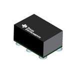
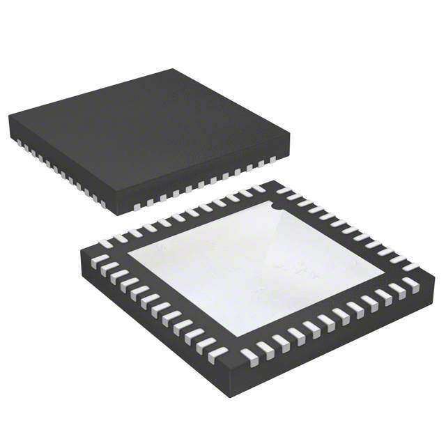
| 产品图片 |
|
| rohs | 符合RoHS无铅 / 符合限制有害物质指令(RoHS)规范要求 |
| 产品系列 | 开关 IC,电源开关 IC - 配电,Texas Instruments TPS22922YFPR- |
| 数据手册 | |
| 产品型号 | TPS22922YFPR |
| Rds(On) | 14 毫欧 |
| 产品目录页面 | |
| 产品种类 | 电源开关 IC - 配电 |
| 供应商器件封装 | 6-DSBGA,6-WCSP(1.4x0.9) |
| 其它名称 | 296-24677-1 |
| 内部开关 | 是 |
| 包装 | 剪切带 (CT) |
| 商标 | Texas Instruments |
| 安装类型 | 表面贴装 |
| 安装风格 | SMD/SMT |
| 导通电阻—最大值 | 45 mOhms |
| 封装 | Reel |
| 封装/外壳 | 6-XFBGA,DSBGA |
| 封装/箱体 | DSBGA-6 |
| 工作温度 | -40°C ~ 85°C |
| 工作电源电压 | 0.9 V to 3.6 V |
| 工厂包装数量 | 3000 |
| 开关电流—最大值 | 2 A |
| 开关类型 | 通用 |
| 最大功率耗散 | 0.645 W |
| 最大工作温度 | + 85 C |
| 最大输入电压 | 3.6 V |
| 最小工作温度 | - 40 C |
| 最小输入电压 | 0.9 V |
| 标准包装 | 1 |
| 比率-输入:输出 | 1:1 |
| 特性 | 负载释放,压摆率受控型 |
| 电压-负载 | 0.9 V ~ 3.6 V |
| 电压-输入 | 0.9 V ~ 3.6 V |
| 电流-输出(最大值) | 2A |
| 电流限制 | 2 A |
| 空闲时间—最大值 | 139 us |
| 类型 | 通用 |
| 系列 | TPS22922 |
| 输入类型 | 非反相 |
| 输出数 | 1 |
| 输出电流 | 2 A |
| 输出端数量 | 1 Output |
| 输出类型 | P 通道 |
| 运行时间—最大值 | 45 us |


- 商务部:美国ITC正式对集成电路等产品启动337调查
- 曝三星4nm工艺存在良率问题 高通将骁龙8 Gen1或转产台积电
- 太阳诱电将投资9.5亿元在常州建新厂生产MLCC 预计2023年完工
- 英特尔发布欧洲新工厂建设计划 深化IDM 2.0 战略
- 台积电先进制程称霸业界 有大客户加持明年业绩稳了
- 达到5530亿美元!SIA预计今年全球半导体销售额将创下新高
- 英特尔拟将自动驾驶子公司Mobileye上市 估值或超500亿美元
- 三星加码芯片和SET,合并消费电子和移动部门,撤换高东真等 CEO
- 三星电子宣布重大人事变动 还合并消费电子和移动部门
- 海关总署:前11个月进口集成电路产品价值2.52万亿元 增长14.8%


PDF Datasheet 数据手册内容提取
Product Sample & Technical Tools & Support & Folder Buy Documents Software Community TPS22921,TPS22922,TPS22922B SLVS749C–NOVEMBER2008–REVISEDJANUARY2015 TPS2292x 3.6-V, 2-A, 14-mΩ ON-Resistance Load Switch With Controlled Turnon 1 Features 2 Applications • IntegratedP-ChannelLoadSwitch • PDAs 1 • InputVoltage:0.9Vto3.6V • CellPhones • ON-Resistance(TypicalValues) • GPSDevices – r =14mΩ atV =3.6V • MP3Players ON IN – r =20mΩ atV =2.5V • PeripheralPorts ON IN – r =33mΩ atV =1.8V • PortableMediaPlayers ON IN – r =67mΩ atV =1.2V • RFModules ON IN – r =116mΩatV =1.0V ON IN 3 Description • 2-AMaximumContinuousSwitchCurrent TPS22921, TPS22922, and TPS22922B are small, • QuiescentCurrent: low r load switches with controlled turnon. The ON – Typical78nAat1.8V TPS22921/2/2B contains a P-channel MOSFET that • ShutdownCurrent: can operate over an input voltage range of 0.9 V to 3.6 V. The switch is controlled by an on/off input – Typical35nAat1.8V (ON), which can interface directly with low-voltage • LowThresholdControlInputEnabletheuseof control signals. In TPS22922 and in TPS22922B, a 1.2V,1.8V,2.5V,or3.3VLogic 65-Ω on-chip load resistor is added for output quick • ControlledSlewRatetoAvoidInrushCurrents discharge when the switch is turned off. The rise time (slew rate) of the device is internally controlled in – t =30 μsatV =1.8V(TPS22921/2) R IN order to avoid inrush current: TPS22921 and – tR=200μsatVIN =1.8V(TPS22922B) TPS22922 feature a 30-μs rise time, whereas • QuickOutputDischarge(TPS22922/2B) TPS22922Bis200 μs. • ESDPerformanceTestedPerJESD22 TPS22921, TPS22922, and TPS22922B feature low – 3000-VHumanBodyModel quiescent and shutdown currents and are available in (A114-B,ClassII) space-saving 6-pin wafer-chip-scale packages DSBGA(WCSP:YZPandYZTwith0.5-mmpitchand – 1000-VCharged-DeviceModel(C101) YFP with 0.4-mm pitch) which make them ideal for • SixTerminalWafer-Chip-ScaleDSBGAPackage portable electronics. The devices are characterized (nominaldimensionsshown-seeMechanical, for operation over the free-air temperature range of Packaging,andOrderableInformation fordetails) –40°Cto85°C. – 0.9-mm ×1.4-mm,0.5-mmPitch, DeviceInformation(1) 0.5mmHeight(YZP) PARTNUMBER PACKAGE BODYSIZE(NOM) – 0.9-mm ×1.4-mm,0.5-mmPitch, YZT 0.625mmHeight(YZT) 0.9mm×1.4mm TPS22921(1) YZP – 0.8-mm ×1.2-mm,0.4-mmPitch, YFP 0.8mm×1.2mm 0.5-mmHeight(YFP) TPS22922 YZP 0.9mm×1.4mm TPS22922B YFP 0.8mm×1.2mm (1) For all available packages, see the orderable addendum at theendofthedatasheet. 4 Typical Application LOAD VBATT SMPS VIN VOUT (see Note A) ON TPS22921/22/22B CIN= 1µF CL OFF CL RL GND GND GND A. Switched-modepowersupply 1 An IMPORTANT NOTICE at the end of this data sheet addresses availability, warranty, changes, use in safety-critical applications, intellectualpropertymattersandotherimportantdisclaimers.UNLESSOTHERWISENOTED,thisdocumentcontainsPRODUCTION DATA.
TPS22921,TPS22922,TPS22922B SLVS749C–NOVEMBER2008–REVISEDJANUARY2015 www.ti.com Table of Contents 1 Features.................................................................. 1 8.14 TypicalCharacteristics..........................................10 2 Applications........................................................... 1 9 ParameterMeasurementInformation................19 3 Description............................................................. 1 10 DetailedDescription........................................... 20 4 TypicalApplication................................................ 1 10.1 Overview...............................................................20 5 RevisionHistory..................................................... 2 10.2 FunctionalBlockDiagram.....................................20 10.3 FeatureDescription...............................................20 6 DeviceComparisonTable..................................... 3 10.4 DeviceFunctionalModes......................................20 7 PinConfigurationandFunctions......................... 3 11 ApplicationandImplementation........................ 21 8 Specifications......................................................... 4 11.1 ApplicationInformation..........................................21 8.1 AbsoluteMaximumRatings .....................................4 11.2 TypicalApplication ...............................................21 8.2 ESDRatings..............................................................4 12 PowerSupplyRecommendations..................... 24 8.3 RecommendedOperatingConditions.......................4 13 Layout................................................................... 24 8.4 ThermalInformation..................................................4 8.5 ElectricalCharacteristics...........................................5 13.1 LayoutGuidelines.................................................24 8.6 SwitchingCharacteristics:V =0.9V......................6 13.2 LayoutExample....................................................24 IN 8.7 SwitchingCharacteristics:V =1V.........................6 14 DeviceandDocumentationSupport................. 25 IN 8.8 SwitchingCharacteristics:V =1.1V......................7 14.1 RelatedLinks........................................................25 IN 8.9 SwitchingCharacteristics:V =1.2V......................7 14.2 Trademarks...........................................................25 IN 8.10 SwitchingCharacteristics:V =1.8V....................8 14.3 ElectrostaticDischargeCaution............................25 IN 8.11 SwitchingCharacteristics:V =2.5V....................8 14.4 Glossary................................................................25 IN 8.12 SwitchingCharacteristics:V =3V.......................9 15 Mechanical,Packaging,andOrderable IN 8.13 SwitchingCharacteristics:V =3.6V....................9 Information........................................................... 25 IN 5 Revision History NOTE:Pagenumbersforpreviousrevisionsmaydifferfrompagenumbersinthecurrentversion. ChangesfromRevisionB(May2012)toRevisionC Page • AddedPinConfigurationandFunctionssection,ESDRatingtable,FeatureDescriptionsection,DeviceFunctional Modes,ApplicationandImplementationsection,PowerSupplyRecommendationssection,Layoutsection,Device andDocumentationSupportsection,andMechanical,Packaging,andOrderableInformationsection .............................. 1 ChangesfromRevisionA(December2008)toRevisionB Page • ChangedFeatureFrom:Ultra-LowQuiescentCurrent:78nAat1.8VTo:Ultra-LowQuiescentCurrent:Typical78 nAat1.8V.............................................................................................................................................................................. 1 • ChangedFeatureFrom:Typical78nAat1.8VTo:Ultra-LowShutdownCurrent:Typical35nAat1.8V.......................... 1 • ChangedFeatureFrom:SixTerminalWafer-Chip-ScalePackageTo:SixTerminalWafer-Chip-ScalePackage (nominaldimensionsshown-seeaddendumfordetails....................................................................................................... 1 • ChangedFeatureFrom:0.5-mmHeightTo:0.5-mmHeight(YFP)....................................................................................... 1 • ChangedTPS22921QUICKOUTPUTDISCHARGEFrom:-To:No.................................................................................... 3 • ChangedtheformatoftheELECTRICALCHARACTERISTICSTestConditionsFrom:V =1-VtoV =1V....................5 IN IN • DeletedNote1-RL_CHIP=120ΩfromallSWITCHINGCHARACTERISTICStables....................................................... 6 • ChangedFigure50titleFrom:t ResponseTo:t Response........................................................................................ 17 OFF ON ChangesfromOriginal(November2008)toRevisionA Page • AddedNoteAtotheTYPICALAPPLICATIONcircuit............................................................................................................ 1 2 SubmitDocumentationFeedback Copyright©2008–2015,TexasInstrumentsIncorporated ProductFolderLinks:TPS22921 TPS22922 TPS22922B
TPS22921,TPS22922,TPS22922B www.ti.com SLVS749C–NOVEMBER2008–REVISEDJANUARY2015 6 Device Comparison Table RON(TAYTP1).8V (TRYIPSEatT1IM.8EV) QDUISICCKHAORUGTPEU(1T) MACXURORUETNPTUT ENABLE TPS22921 33mΩ 30μs No 2A Activehigh TPS22922 33mΩ 30μs Yes 2A Activehigh TPS22922B 33mΩ 200μs Yes 2A Activehigh (1) Thisfeaturedischargestheoutputoftheswitchtogroundthrougha120-Ωresistor,preventingthe outputfromfloating. 7 Pin Configuration and Functions YFP,YZP,ANDYZT PACKAGES C C B B A A 2 1 1 2 Laser Marking View Bump View PinAssignments C ON GND B V V IN OUT A V V IN OUT 2 1 PinFunctions PIN I/O DESCRIPTION NO. NAME A1 V O Switchoutput OUT A2 V I Switchinput.Useabypasscapacitortoground(ceramic) IN B1 V O Switchoutput OUT B2 V I Switchinput.Useabypasscapacitortoground(ceramic) IN C1 GND – Ground C2 ON I Switchcontrolinput,activehigh.Donotleavefloating Copyright©2008–2015,TexasInstrumentsIncorporated SubmitDocumentationFeedback 3 ProductFolderLinks:TPS22921 TPS22922 TPS22922B
TPS22921,TPS22922,TPS22922B SLVS749C–NOVEMBER2008–REVISEDJANUARY2015 www.ti.com 8 Specifications 8.1 Absolute Maximum Ratings(1) MIN MAX UNIT V Inputvoltage –0.3 4 V IN V Outputvoltage V +0.3 V OUT IN V Inputvoltage –0.3 4 V ON P PowerdissipationatT =25°C 0.645 W A I Maximumcontinuousswitchcurrent 2 A MAX T Operatingfree-airtemperature –40 85 °C A T Maximumleadtemperature(10-ssolderingtime) 300 °C lead T Storagetemperature –65 150 °C stg (1) StressesbeyondthoselistedunderAbsoluteMaximumRatingsmaycausepermanentdamagetothedevice.Thesearestressratings only,andfunctionaloperationofthedeviceattheseoranyotherconditionsbeyondthoseindicatedunderRecommendedOperating Conditionsisnotimplied.Exposuretoabsolute-maximum-ratedconditionsforextendedperiodsmayaffectdevicereliability. 8.2 ESD Ratings VALUE UNIT Humanbodymodel(HBM),perANSI/ESDA/JEDECJS-001(1) ±3000 V Electrostatic Charged-devicemodel(CDM),perJEDECspecificationJESD22-C101(2) ±1000 V (ESD) discharge Machinemodel(MM) ±300 (1) JEDECdocumentJEP155statesthat500-VHBMallowssafemanufacturingwithastandardESDcontrolprocess. (2) JEDECdocumentJEP157statesthat250-VCDMallowssafemanufacturingwithastandardESDcontrolprocess. 8.3 Recommended Operating Conditions MIN MAX UNIT V Inputvoltagerange 0.9 3.6 V IN V Outputvoltagerange V V OUT IN V High-levelinputvoltage,ON 0.85 3.6 V IH V Low-levelinputvoltage,ON 0.4 V IL C Inputcapacitor 1(1) µF IN (1) RefertoApplicationInformation. 8.4 Thermal Information TPS22921,TPS22922, TPS22921 TPS22922B THERMALMETRIC(1) UNIT YFP YZP YZT 6PINS R Junction-to-ambientthermalresistance 125.1 131 120.7 θJA R Junction-to-case(top)thermalresistance 1.4 1.3 2.1 θJC(top) R Junction-to-boardthermalresistance 26 22.6 26.4 °C/W θJB ψ Junction-to-topcharacterizationparameter 0.3 5.2 3.7 JT ψ Junction-to-boardcharacterizationparameter 26 22.6 26.4 JB (1) Formoreinformationabouttraditionalandnewthermalmetrics,seetheICPackageThermalMetricsapplicationreport,SPRA953. 4 SubmitDocumentationFeedback Copyright©2008–2015,TexasInstrumentsIncorporated ProductFolderLinks:TPS22921 TPS22922 TPS22922B
TPS22921,TPS22922,TPS22922B www.ti.com SLVS749C–NOVEMBER2008–REVISEDJANUARY2015 8.5 Electrical Characteristics V =0.9Vto3.6V,T =–40°Cto85°C(unlessotherwisenoted) IN A PARAMETER TESTCONDITIONS T MIN TYP(1) MAX UNIT A V =1V Full 30 120 IN I Quiescentcurrent I =0mA V =1.8V Full 78 235 nA Q OUT IN V =3.6V Full 200 880 IN V =1V Full 10 210 IN V =GND, I OFF-statesupplycurrent ON V =1.8V Full 35 260 nA IN(OFF) OUT=Open IN V =3.6V Full 120 700 IN V =1V Full 12 140 IN V =GND, I OFF-stateswitchcurrent ON V =1.8V Full 50 230 nA IN(LEAKAGE) V =0V IN OUT V =3.6V Full 130 610 IN 25°C 14 45 V =3.6V IN Full 50 25°C 20 55 V =2.5V IN Full 60 25°C 33 65 V =1.8V IN Full 75 r ON-stateresistance I =–200mA mΩ ON OUT 25°C 67 100 V =1.2V IN Full 120 25°C 82 150 V =1.1V IN Full 160 25°C 116 160 V =1V IN Full 170 V =3.3V,V =0V,I =30mA r Outputpulldownresistance IN ON OUT 25°C 65 120 Ω PD (TPS22922andTPS22922Bonly) I ONinputleakagecurrent V =1.1Vto3.6VorGND Full 25 nA ON ON (1) TypicalvaluesareatthespecifiedV andT =25°C. IN A Copyright©2008–2015,TexasInstrumentsIncorporated SubmitDocumentationFeedback 5 ProductFolderLinks:TPS22921 TPS22922 TPS22922B
TPS22921,TPS22922,TPS22922B SLVS749C–NOVEMBER2008–REVISEDJANUARY2015 www.ti.com 8.6 Switching Characteristics: V = 0.9 V IN V =0.9V,T =25°C(unlessotherwisenoted) IN A TPS22921 TPS22922 TPS22922B PARAMETER TESTCONDITIONS UNIT MIN TYP MAX MIN TYP MAX MIN TYP MAX C =0.1μF 121 121 638 L t Turn-ONtime R =500Ω C =1μF 160 160 712 μs ON L L C =3μF 188 188 799 L C =0.1μF 46 40 40 L t Turn-OFFtime R =500Ω C =1μF 308 279 279 μs OFF L L C =3μF 975 807 807 L C =0.1μF 60 60 462 L t V risetime R =500Ω C =1μF 85 85 465 μs r OUT L L C =3μF 107 107 507 L C =0.1μF 119 51 51 L t V falltime R =500Ω C =1μF 969 434 434 μs f OUT L L C =3μF 3174 1264 1264 L 8.7 Switching Characteristics: V = 1 V IN V =1V,T =25°C(unlessotherwisenoted) IN A TPS22921 TPS22922 TPS22922B PARAMETER TESTCONDITIONS UNIT MIN TYP MAX MIN TYP MAX MIN TYP MAX C =0.1μF 105 105 549 L t Turn-ONtime R =500Ω C =1μF 136 136 613 μs ON L L C =3μF 157 157 683 L C =0.1μF 46 28 28 L t Turn-OFFtime R =500Ω C =1μF 309 186 186 μs OFF L L C =3μF 983 511 511 L C =0.1μF 51 51 386 L t V risetime R =500Ω C =1μF 78 78 388 μs r OUT L L C =3μF 88 88 419 L C =0.1μF 121 34 34 L t V falltime R =500Ω C =1μF 986 306 306 μs f OUT L L C =3μF 3300 908 908 L 6 SubmitDocumentationFeedback Copyright©2008–2015,TexasInstrumentsIncorporated ProductFolderLinks:TPS22921 TPS22922 TPS22922B
TPS22921,TPS22922,TPS22922B www.ti.com SLVS749C–NOVEMBER2008–REVISEDJANUARY2015 8.8 Switching Characteristics: V = 1.1 V IN V =1.1V,T =25°C(unlessotherwisenoted) IN A TPS22921 TPS22922 TPS22922B PARAMETER TESTCONDITIONS UNIT MIN TYP MAX MIN TYP MAX MIN TYP MAX C =0.1μF 91 93 484 L t Turn-ONtime R =500Ω C =1μF 118 118 540 μs ON L L C =3μF 137 137 599 L C =0.1μF 44 21 21 L t Turn-OFFtime R =500Ω C =1μF 311 144 144 μs OFF L L C =3μF 99 383 383 L C =0.1μF 46 46 335 L t V risetime R =500Ω C =1μF 60 60 336 μs r OUT L L C =3μF 76 76 363 L C =0.1μF 122 29 29 L t V falltime R =500Ω C =1μF 1000 224 224 μs f OUT L L C =3μF 3300 732 732 L 8.9 Switching Characteristics: V = 1.2 V IN V =1.2V,T =25°C(unlessotherwisenoted) IN A TPS22921 TPS22922 TPS22922B PARAMETER TESTCONDITIONS UNIT MIN TYP MAX MIN TYP MAX MIN TYP MAX C =0.1μF 83 83 435 L t Turn-ONtime R =500Ω C =1μF 103 103 485 μs ON L L C =3μF 122 122 536 L C =0.1μF 44 17 17 L t Turn-OFFtime R =500Ω C =1μF 312 117 117 μs OFF L L C =3μF 1000 319 319 L C =0.1μF 41 41 301 L t V risetime R =500Ω C =1μF 54 54 302 μs r OUT L L C =3μF 67 67 325 L C =0.1μF 123 25 25 L t V falltime R =500Ω C =1μF 1000 214 214 μs f OUT L L C =3μF 3400 632 632 L Copyright©2008–2015,TexasInstrumentsIncorporated SubmitDocumentationFeedback 7 ProductFolderLinks:TPS22921 TPS22922 TPS22922B
TPS22921,TPS22922,TPS22922B SLVS749C–NOVEMBER2008–REVISEDJANUARY2015 www.ti.com 8.10 Switching Characteristics: V = 1.8 V IN V =1.8V,T =25°C(unlessotherwisenoted) IN A TPS22921 TPS22922 TPS22922B PARAMETER TESTCONDITIONS UNIT MIN TYP MAX MIN TYP MAX MIN TYP MAX C =0.1μF 54 54 282 L t Turn-ONtime R =500Ω C =1μF 67 67 314 μs ON L L C =3μF 78 78 344 L C =0.1μF 41 10 10 L t Turn-OFFtime R =500Ω C =1μF 312 67 67 μs OFF L L C =3μF 1000 181 181 L C =0.1μF 30 30 200 L t V risetime R =500Ω C =1μF 37 37 202 μs r OUT L L C =3μF 47 47 219 L C =0.1μF 121 17 17 L t V falltime R =500Ω C =1μF 1000 158 158 μs f OUT L L C =3μF 3450 461 461 L 8.11 Switching Characteristics: V = 2.5 V IN V =2.5V,T =25°C(unlessotherwisenoted) IN A TPS22921 TPS22922 TPS22922B PARAMETER TESTCONDITIONS UNIT MIN TYP MAX MIN TYP MAX MIN TYP MAX C =0.1μF 40 40 211 L t Turn-ONtime R =500Ω C =1μF 50 50 233 μs ON L L C =3μF 59 59 256 L C =0.1μF 41 10 10 L t Turn-OFFtime R =500Ω C =1μF 316 56 56 μs OFF L L C =3μF 1000 153 153 L C =0.1μF 23 23 164 L t V risetime R =500Ω C =1μF 29 29 165 μs r OUT L L C =3μF 38 38 177 L C =0.1μF 122 16 16 L t V falltime R =500Ω C =1μF 1086 147 147 μs f OUT L L C =3μF 3600 430 430 L 8 SubmitDocumentationFeedback Copyright©2008–2015,TexasInstrumentsIncorporated ProductFolderLinks:TPS22921 TPS22922 TPS22922B
TPS22921,TPS22922,TPS22922B www.ti.com SLVS749C–NOVEMBER2008–REVISEDJANUARY2015 8.12 Switching Characteristics: V = 3 V IN V =3V,T =25°C(unlessotherwisenoted) IN A TPS22921 TPS22922 TPS22922B PARAMETER TESTCONDITIONS UNIT MIN TYP MAX MIN TYP MAX MIN TYP MAX C =0.1μF 30 30 182 L t Turn-ONtime R =500Ω C =1μF 38 38 201 μs ON L L C =3μF 45 45 221 L C =0.1μF 40 10 10 L t Turn-OFFtime R =500Ω C =1μF 353 51 51 μs OFF L L C =3μF 1036 139 139 L C =0.1μF 20 20 149 L t V risetime R =500Ω C =1μF 25 25 150 μs r OUT L L C =3μF 33 33 161 L C =0.1μF 104 15 15 L t V falltime R =500Ω C =1μF 1030 143 143 μs f OUT L L C =3μF 3230 419 419 L 8.13 Switching Characteristics: V = 3.6 V IN V =3.6V,T =25°C(unlessotherwisenoted) IN A TPS22921 TPS22922 TPS22922B PARAMETER TESTCONDITIONS UNIT MIN TYP MAX MIN TYP MAX MIN TYP MAX C =0.1μF 30 30 159 L t Turn-ONtime R =500Ω C =1μF 38 38 175 μs ON L L C =3μF 45 45 193 L C =0.1μF 42 10 10 L t Turn-OFFtime R =500Ω C =1μF 310 51 51 μs OFF L L C =3μF 988 139 139 L C =0.1μF 20 20 137 L t V risetime R =500Ω C =1μF 25 25 138 μs r OUT L L C =3μF 33 33 148 L C =0.1μF 120 15 15 L t V falltime R =500Ω C =1μF 1100 143 143 μs f OUT L L C =3μF 3600 419 419 L Copyright©2008–2015,TexasInstrumentsIncorporated SubmitDocumentationFeedback 9 ProductFolderLinks:TPS22921 TPS22922 TPS22922B
TPS22921,TPS22922,TPS22922B SLVS749C–NOVEMBER2008–REVISEDJANUARY2015 www.ti.com 8.14 Typical Characteristics 8.14.1 TypicalDCCharacteristics 0.45 0.024 0.40 0.023 0.35 ΩN-State Resistance, r()ON0000....12235050 WN-State Resistance, r()ON 00.0.00.202221 O O 0.10 0.019 0.05 0.00 0.018 0.7 1.2 1.7 2.2 2.7 3.2 3.7 -40.00 25.00 85.00 InputVoltage,VIN(V) Temperature (C) Figure1.rONvsVIN Figure2. rONvsTemperature(VIN=3.3V) 500 225 450 200 400 175 350 VoltageDrop(mV) 122350500000 Vdrop= 1.8V VVddrroopp== 11..02VV nAQuiescent Current, I()IN11105720055. Vdrop= 2.5V 100 50 Vdrop= 3.3V 50 25 0 0.0 0.2 0.4 0.6 0.8 1.0 1.2 1.4 1.6 1.8 2.0 00.5 1.0 1.5 2.0 2.5 3.0 3.5 4.0 Load Current (A) InputVoltage,VIN(V) Figure3.VoltageDropvsLoadCurrent Figure4.QuiescentCurrentvsV (V =V ) IN ON IN 300 275 250 250 225 200 nAQuiescent Current, I()IN112050000 Leakage Current, I(nA)IN11110572700555 50 50 25 0 0 –40 25 85 –40 25 85 Temperature (°C) Temperature (°C) Figure5.QuiescentCurrentvsTemperature Figure6.I LeakageCurrentvsTemperature(V =3.3V) IN IN (V =3.3V,I =0mA) IN OUT 10 SubmitDocumentationFeedback Copyright©2008–2015,TexasInstrumentsIncorporated ProductFolderLinks:TPS22921 TPS22922 TPS22922B
TPS22921,TPS22922,TPS22922B www.ti.com SLVS749C–NOVEMBER2008–REVISEDJANUARY2015 Typical DC Characteristics (continued) 140 160 120 140 120 100 A) Leakage Current, I(nIN 6800 IOFF Current (nA)IN1680000 40 40 20 20 0 0 0.5 1.0 1.5 2.0 2.5 3.0 3.5 4.0 0.5 1.0 1.5 2.0 2.5 3.0 3.5 4.0 InputVoltage,VIN(V) InputVoltage,VIN(V) Figure7. LeakageCurrentvsVIN Figure8.IIN(OFF)vsVIN(VON=0V) 275 4.0 —VIN= 3.6V 250 3.5 —VIN= 3.3V A)220205 3.0 ———VVVIIINNN=== 321..V58VV Current (OFF), I(nIN111527055 V(V)OUT212...055 —————VVVVVIIIIINNNNN===== 11110....V5219VVVV Quiescent 10705 1.0 0.5 50 25 0.0 0 –0.5 –40 25 85 0.3 0.4 0.5 0.6 0.7 0.8 Temperature (°C) InputVoltage,VON(V) Figure9.I (OFF)vsTemperature(V =3.3V) Figure10.ON-InputThreshold IN IN 8.14.2 TypicalACCharacteristics(TPS22921) 50.0 130 120 47.5 110 45.0 100 tfall 42.5 TOFF 90 µs/t()ONOFF4307..05 t/t)(µsrf 678000 t35.0 50 32.5 40 30 30.0 tON 20 27.5 10 trise 25.0 0 –50–40–30–20–10 0 10 20 30 40 50 60 70 80 90 100 –50 –40 –30 –20 –10 0 10 20 30 40 50 60 70 80 90 100 Temperature,TA(°C) Temperature (°C) Figure11.t /t vsTemperature(V =3.3V) Figure12.t /t vsTemperature(V =3.3V) ON OFF IN rise fall IN Copyright©2008–2015,TexasInstrumentsIncorporated SubmitDocumentationFeedback 11 ProductFolderLinks:TPS22921 TPS22922 TPS22922B
TPS22921,TPS22922,TPS22922B SLVS749C–NOVEMBER2008–REVISEDJANUARY2015 www.ti.com 8.14.3 TypicalACCharacteristics(TPS22922) 50 40 45 35 40 tOFF(TPS22922) tfall(TPS22922) 30 35 25 µst/t()ONOFF 223050 tON t/t(s)mrisefall 1250 trise 15 10 10 5 5 0 0 –40 0 25 70 85 –40 0 25 70 85 Temperature,TA(°C) Temperature (°C) Figure13.tON/tOFFvsTemperature(VIN=3.3V) Figure14.trise/tfallvsTemperature(VIN=3.3V) 8.14.4 TypicalACCharacteristics(TPS22922B) 200 160 150 180 140 160 130 tON 120 trise 140 110 100 µst/t()ONOFF11802000 t/t)(µsrf 789000 60 60 50 40 40 30 tfall 20 TOFF 20 10 0 0 –50–40–30–20–10 0 10 20 30 40 50 60 70 80 90 100 –50 –40 –30 –20 –10 0 10 20 30 40 50 60 70 80 90 100 Temperature,TA(°C) Temperature (°C) Figure15. tON/tOFFvsTemperature(VIN=3.3V) Figure16.trise/tfallvsTemperature(VIN=3.3V) 8.14.5 TypicalACCharacteristics(TPS22921andTPS22922) 3.0 0.03 3.0 0.03 2.8 RL= 500W 2.8 RL= 500W 222...462 VCILN== 1 3µ.3FV 222...462 VCILN== 3 3µ.3FV 2.0 ON = 1.8V 0.02 2.0 ON = 1.8V 0.02 1.8 1.8 ON InputVoltage (V) 1011001.......4406682 tON= 40µs IOUT= 6.6 mA 0.01 Output Current (A) ON InputVoltage (V) 1011001.......4406682 tONI=O U4T0=µ s6.6 mA 0.01 Output Current (A) 0.2 0.2 0.0 0.00 0.0 0.00 –0.2 –0.2 –0.4 –0.4 –0.6 –0.6 –0.8 –0.8 –1.0 –0.01 –1.0 –0.01 Figure17. t Response Figure18. t Response ON ON 12 SubmitDocumentationFeedback Copyright©2008–2015,TexasInstrumentsIncorporated ProductFolderLinks:TPS22921 TPS22922 TPS22922B
TPS22921,TPS22922,TPS22922B www.ti.com SLVS749C–NOVEMBER2008–REVISEDJANUARY2015 Typical AC Characteristics (TPS22921 and TPS22922) (continued) 1.2 1.2 1.1 RL= 500W 1.1 RL= 500W 1.0 VIN= 1 V 1.0 VIN= 1V 0.9 CL= 0.1µF 0.9 CL= 1µF 0.8 ON = 0.85 V 0.01 0.8 ON = 0.85V 0.01 ON Input Voltage (V) 0000000.......3614572 tON= 100µs IOUT= 2 mA ON InputVoltage (V) 0000000.......3614572 tON= 145 µs IOUT= 2 mA Output Current (A) 0.0 0.00 0.0 0.00 –0.1 –0.1 –0.2 –0.2 –0.3 –0.3 –0.4 –0.4 Figure19. tONResponse Figure20. tONResponse 1.2 1.1 1.0 ON = 0.85V 0.9 0.8 RL= 500W 0.01 ON InputVoltage (V) 0000000.......3614572 tIOONUT= =1 620 m µAs VCILN== 3 1µVF Output Current (A) 0.0 0.00 –0.1 –0.2 –0.3 –0.4 Figure21. t Response ON 8.14.6 TypicalACCharacteristics(TPS22921) 1.38 0.014 3.50 0.35 11..3200 RVILN== 5 30.03WV 00..001132 333...420000 RVILN== 1 30.3WV 000...333402 1.10 CL= 0.1µF 0.011 2.80 IOUT CL= 0.1µF 0.28 1.00 0.010 2.60 0.26 V) 0.90 0.009 V) 22..4200 00..2242 e ( 0.80 VON 0.008 e ( 2.00 0.20 nputVoltag 000...765000 000...000000765Current (A) nputVoltag 1111....86420000 0000....11114682 Current (A) Control I 00..4300 IOUT 00..000043Output Control I 001...860000 000...100068 Output 0.20 0.002 0.40 VON 0.04 0.10 0.001 0.20 0.02 0.00 0.00 0.00 0.000 –0.20 –0.02 –0.10 –0.001 –0.40 –0.04 –0.22 –0.002 –0.50 –0.05 –200 0 20 40 60 80 100 120 140 160 180 –2.0 0 2.0 4.0 6.0 8.0 10.0 12.0 14.0 16.0 18.0 Time (µs) Time (µs) Figure22. t Response Figure23. t Response OFF OFF Copyright©2008–2015,TexasInstrumentsIncorporated SubmitDocumentationFeedback 13 ProductFolderLinks:TPS22921 TPS22922 TPS22922B
TPS22921,TPS22922,TPS22922B SLVS749C–NOVEMBER2008–REVISEDJANUARY2015 www.ti.com Typical AC Characteristics (TPS22921) (continued) 1.20 0.012 1.20 0.600 1.10 RL= 500W 0.011 1.10 RL= 10W 0.550 1.00 VIN= 3.3V 0.010 1.00 VIN= 3.3V 0.500 0.90 CL= 3.3µF 0.009 0.90 CL= 3.3µF 0.450 0.80 0.008 0.80 0.400 V) 0.70 0.007 V) 0.70 0.350 e ( 0.60 0.006 e ( 0.60 0.300 Control InputVoltag 00000.....1543200000 VON IOUT 00000.....000000000051243Output Current (A) Control InputVoltag 00000.....5432100000 VON IOUT 00000.....211025505000000Output Current (A) 0.00 0.000 0.00 0.000 –0.10 –0.001 –0.10 –0.050 –0.20 –0.002 –0.20 –0.100 –0.30 –0.003 –0.30 –0.150 –0.40 –0.004 –0.40 –0.200 –3.5–3.0 –2.0 –1.0 0.0 1.0 2.0 3.0 4.0 5.0 6.06.5 –20 0 20 40 60 80 100 120 140 160 180 Time (µs) Time (µs) Figure24. t Response Figure25. t Response OFF OFF 1.20 0.006 1.20 0.12 1.10 RL= 500W 1.10 RL= 10W 0.11 1.00 VIN= 1V 0.005 1.00 VIN= 1V 0.10 0.90 CL= 0.1µF 0.90 CL= 0.1µF 0.09 0.80 0.004 0.80 0.08 V) 0.70 V) 0.70 0.07 e ( 0.60 0.003 e ( 0.60 0.06 Control InputVoltag 00000.....5432100000 VON IOUT 00..000012Output Current (A) Control InputVoltag 00000.....1543200000 VON IOUT 00000.....0000051243 Output Current (A) 0.00 0.000 0.00 0.00 –0.10 –0.10 –0.01 –0.20 –0.001 –0.20 –0.02 –0.30 –0.30 –0.03 –0.40 –0.002 –0.40 –0.04 –20 0 20 40 60 80 100 120 140 160 180 –2.0 0.0 2.0 4.0 6.0 8.0 10.0 12.0 14.0 16.0 18.0 Time (µs) Time (µs) Figure26. t Response Figure27. t Response OFF OFF 1.20 0.006 1.20 0.12 1.10 RL= 500W 1.10 RL= 10W 0.11 1.00 VIN= 1V 0.005 1.00 VIN= 1V 0.10 0.90 CL= 3.3µF 0.90 CL= 3.3µF 0.09 0.80 0.004 0.80 0.08 V) 0.70 V) 0.70 0.07 e ( 0.60 0.003 e ( 0.60 0.06 Control InputVoltag 00000.....5432100000 VON IOUT 00..000012Output Current (A) Control InputVoltag 00000.....1543200000 VON IOUT 00000.....0000051243 Output Current (A) 0.00 0.000 0.00 0.00 –0.10 –0.10 –0.01 –0.20 –0.001 –0.20 –0.02 –0.30 –0.30 –0.03 –0.40 –0.002 –0.40 –0.04 –500 0 500 1000 1500 2000 2500 3000 3500 4000 4500 –20 0.0 20 40 60 80 100 120 140 160 180 Time (µs) Time (µs) Figure28. t Response Figure29. t Response OFF OFF 14 SubmitDocumentationFeedback Copyright©2008–2015,TexasInstrumentsIncorporated ProductFolderLinks:TPS22921 TPS22922 TPS22922B
TPS22921,TPS22922,TPS22922B www.ti.com SLVS749C–NOVEMBER2008–REVISEDJANUARY2015 8.14.7 TypicalACCharacteristics(TPS22922) 3.0 0.03 3.0 0.03 2.8 RL= 500W 2.8 RL= 500W 2.6 VIN= 3.3V 2.6 VIN= 3.3V 22..42 CL= 0.1µF 22..42 CL= 1µF 2.0 ON = 1.8V 0.02 2.0 ON = 1.8V 0.02 1.8 1.8 ON InputVoltage (V) 1011001.......4406682 IOUT=t O6F.6F m= A8 µs 0.01 Output Current (A) ON InputVoltage (V) 1011001.......4406682 IOUT= 6.6 mA 0.01 Output Current (A) 0.2 0.2 0.0 0.00 0.0 0.00 –0.2 –0.2 tOFF= 50 µs –0.4 –0.4 –0.6 –0.6 –0.8 –0.8 –1.0 –0.01 –1.0 –0.01 Figure30. t Response Figure31. t Response OFF OFF 3.0 0.03 1.2 2.8 RL= 500W 1.1 RL= 500W 2.6 VIN= 3.3V 1.0 VIN= 1V 22..42 CL= 3µF 0.9 ON = 0.85V CL= 0.1µF 2.0 ON = 1.8V 0.02 0.8 0.01 1.8 0.7 ON InputVoltage (V) 1011001.......4406682 IOUT= 6.6 mA 0.01 Output Current (A) ON InputVoltage (V) 00000.....36452 IOUT= 2 mA Output Current (A) 0.2 tOFF= 90 µs 0.1 tOFF= 20 µs 0.0 0.00 0.0 0.00 –0.2 –0.1 –0.4 –0.2 –0.6 –0.8 –0.3 –1.0 –0.01 –0.4 Figure32. t Response Figure33. t Response OFF OFF 1.2 1.2 1.1 RL= 500W 1.1 RL= 500W 1.0 VIN= 1V 1.0 VIN= 1V 0.9 ON = 0.85V CL= 1µF 0.9 ON = 0.85V CL= 3µF 0.8 0.01 0.8 0.01 0.7 0.7 ON InputVoltage (V) 00000.....36452 IOUT= 2 mA tOFF= 240 µs Output Current (A) ON InputVoltage (V) 00000.....36452 IOUT= 2 mA Output Current (A) 0.1 0.1 tOFF= 400µs 0.0 0.00 0.0 0.00 –0.1 –0.1 –0.2 –0.2 –0.3 –0.3 –0.4 –0.4 Figure34. t Response Figure35. t Response OFF OFF Copyright©2008–2015,TexasInstrumentsIncorporated SubmitDocumentationFeedback 15 ProductFolderLinks:TPS22921 TPS22922 TPS22922B
TPS22921,TPS22922,TPS22922B SLVS749C–NOVEMBER2008–REVISEDJANUARY2015 www.ti.com 8.14.8 TypicalACCharacteristics(TPS22922B) 2.50 10.00 2.50 499.9 2.40 2.40 9.00 450.0 2.20 2.20 2.00 8.00 2.00 400.0 1.80 7.00 1.80 350.0 1.60 6.00 1.60 300.0 1.40 1.40 Control Input Voltage (V)–––––––11000000010011..............2086420260482400000000000000 VON IOUT RVCILLN=== 50 30.1.03 µVWF –––––54321012345......000000.....0000000000000000Output Current (mA) Control Input Voltage (V)–––––––11000000010011..............2086420260482400000000000000 VON IOUT RVCILLN=== 10 30.1.3W µVF –––––2211505112250500.0005050000.00.0000....00000....0000Output Current (mA) –1.50 –6.00 –1.50 –300.0 –50 0 50 100 150 200 250 300 350 400 450 –100 0 100 200 300 400 500 600 700 800 900 Time (µs) Time (µs) Figure36. tONResponse Figure37. tONResponse 2.50 10.00 2.50 499.9 2.40 2.40 9.00 450.0 2.20 2.20 2.00 8.00 2.00 400.0 1.80 7.00 1.80 350.0 1.60 6.00 1.60 300.0 Control Input Voltage (V)–––––––111000000010011...............420864202604824000000000000000 VON IOUT RVCILLN=== 53 30.3.03µ VWF –––––54321012345......000000.....0000000000000000Output Current (mA) Control Input Voltage (V)–––––––111000000010011...............420864202604824000000000000000 VON IOUT RVCILLN=== 13 30.3.3W µVF –––––2211505112250500.0005050000.00.0000....00000....0000Output Current (mA) –1.50 –6.00 –1.50 –300.0 –100 0 100 200 300 400 500 600 700 800 900 –100 0 100 200 300 400 500 600 700 800 900 Time (ms) Time (ms) Figure38. tONResponse Figure39. tONResponse 2.50 5.00 2.50 249.9 2.40 2.40 4.50 220.0 22..2000 4.00 22..2000 200.0 180.0 1.80 3.50 1.80 160.0 11..6400 3.00 11..6400 140.0 V) 1.20 2.50 V) 1.20 120.0 e ( 1.00 2.00 e ( 1.00 100.0 Control InputVoltag––0000000.......86420240000000 VON IOUT –11000.....5050500000 Output Current (A) Control InputVoltag––0000000.......86420240000000 VON IOUT –8642020000.00....00000.0Output Current (A) –––––01011.....6082400000 RVCILLN=== 50 10.10VµWF ––––1122....05050000 –––––01011.....6082400000 RVCILLN=== 10 10.1VWµF –––––114680200000...000..00 –1.50 –3.00 –1.50 –150.0 –200 0 200 400 600 800 1000 1200 1400 1600 1800 –200 0 200 400 600 800 1000 1200 1400 1600 1800 Time (µs) Time (µs) Figure40. t Response Figure41. t Response ON ON 16 SubmitDocumentationFeedback Copyright©2008–2015,TexasInstrumentsIncorporated ProductFolderLinks:TPS22921 TPS22922 TPS22922B
TPS22921,TPS22922,TPS22922B www.ti.com SLVS749C–NOVEMBER2008–REVISEDJANUARY2015 Typical AC Characteristics (TPS22922B) (continued) 2.50 5.00 2.50 249.9 2.40 2.40 4.50 220.0 22..2000 4.00 22..2000 200.0 180.0 1.80 3.50 1.80 160.0 11..6400 3.00 11..6400 140.0 V) 1.20 2.50 V) 1.20 120.0 Control Input Voltage (––10000000........0864202400000000 VON IOUT –211000.....05050.5000000Output Current (mA) Control Input Voltage (––10000000........0864202400000000 VON IOUT 1–86420020000.000.....00000.00Output Current (mA) –––––01011.....6082400000 RVCILLN=== 53 10.3 0VµWF ––––1122....05050000 –––––01011.....6082400000 RVCILLN=== 13 10.3 VWµF –––––114680200000...000..00 –1.50 –3.00 –1.50 –150.0 –200 0 200 400 600 800 1000 1200 1400 1600 1800 –500 0 500 1000 1500 2000 2500 3000 3500 4000 4500 Time (µs) Time (µs) Figure42. t Response Figure43. t Response ON ON 2.50 10.00 2.50 499.9 2.40 2.40 9.00 450.0 2.20 2.20 2.00 8.00 2.00 400.0 1.80 7.00 1.80 350.0 1.60 6.00 1.60 300.0 1.40 1.40 Control Input Voltage (V)–––––––11000000010011..............2086420260482400000000000000 VON IOUT RVCILLN=== 50 30.1.03µ WVF –––––54321012345......000000.....0000000000000000Output Current (mA) Control Input Voltage (V)–––––––11000000010011..............2086420260482400000000000000 VON IOUT RVCILLN=== 10 30.1.3Wµ VF –––––2211505112250500.0005050000.00.0000....00000....0000Output Current (mA) –1.50 –6.00 –1.50 –300.0 –10 0 10 20 30 40 50 60 70 80 90 –10 0 10 20 30 40 50 60 70 80 90 Time (µs) Time (µs) Figure44. tOFFResponse Figure45. tOFFResponse 2.50 10.00 2.50 499.9 2.40 2.40 9.00 450.0 2.20 2.20 2.00 8.00 2.00 400.0 1.80 7.00 1.80 350.0 1.60 6.00 1.60 300.0 1.40 1.40 V) 1.20 5.00 V) 1.20 250.0 Control Input Voltage (––10000000........0864202400000000 VON IOUT –432101.....00000.0000000Output Current (mA) Control Input Voltage (––10000000........0864202400000000 VON IOUT –2115050500.00000.00....0000Output Current (mA) –0.60 RL= 500W –2.00 –0.60 RL= 10W –100.0 –0.80 VIN= 3.3 V –3.00 –0.80 VIN= 3.3 V –150.0 ––11..0200 CL= 3.3µF ––45..0000 ––11..0200 CL= 3.3µF ––220500..00 –1.40 –1.40 –1.50 –6.00 –1.50 –300.0 –200 0 200 400 600 800 1000 1200 1400 1600 1800 –50 0 50 100 150 200 250 300 350 400 450 Time (µs) Time (µs) Figure46. t Response Figure47. t Response OFF OFF Copyright©2008–2015,TexasInstrumentsIncorporated SubmitDocumentationFeedback 17 ProductFolderLinks:TPS22921 TPS22922 TPS22922B
TPS22921,TPS22922,TPS22922B SLVS749C–NOVEMBER2008–REVISEDJANUARY2015 www.ti.com Typical AC Characteristics (TPS22922B) (continued) 2.50 5.00 2.50 249.9 2.40 2.40 220.0 4.50 2.20 2.20 200.0 2.00 4.00 2.00 180.0 1.80 3.50 1.80 160.0 1.60 3.00 1.60 140.0 Control Input Voltage (V)––––111000000000............420864202648000000000000 VON IOUT RVILN== 5 10 0VW –––221100011......505050...505000000000Output Current (mA) Control Input Voltage (V)––––111000000000............420864202648000000000000 VON IOUT RVILN== 1 10 VW 11––––846202024680000.0000000....00000......000000Output Current (mA) ––11..0200 CL= 0.1µF –2.00 ––11..0200 CL= 0.1µF –100.0 –1.40 –2.50 –1.40 –120.0 –1.50 –3.00 –1.50 –150.0 –10 0 10 20 30 40 50 60 70 80 90 –10 0 10 20 30 40 50 60 70 80 90 Time (µs) Time (µs) Figure48. t Response Figure49. t Response OFF OFF 2.50 5.00 2.50 249.9 2.40 2.40 220.0 4.50 2.20 2.20 200.0 2.00 4.00 2.00 180.0 1.80 3.50 1.80 160.0 1.60 3.00 1.60 140.0 Control Input Voltage (V)––––––11100000001001..............4208642026048200000000000000 VON IOUT RVCILLN=== 53 10.3 0VµWF –––––22110011220......505050.....0505500000000000Output Current (mA) Control Input Voltage (V)––––––11000001001001..............4208642026048200000000000000 VOINOUT RVCILLN=== 13 10.3 VWµF –11––––8462012024680000.00000000....0..00000....000000.0Output Current (A) –1.40 –1.40 –120.0 –1.50 –3.00 –1.50 –150.0 –200 0 200 400 600 800 1000 1200 1400 1600 1800 –50 0 50 100 150 200 250 300 350 400 450 Time (µs) Time (µs) Figure50. tONResponse Figure51. tOFFResponse 18 SubmitDocumentationFeedback Copyright©2008–2015,TexasInstrumentsIncorporated ProductFolderLinks:TPS22921 TPS22922 TPS22922B
TPS22921,TPS22922,TPS22922B www.ti.com SLVS749C–NOVEMBER2008–REVISEDJANUARY2015 9 Parameter Measurement Information V IN V OUT ON(A) C R L L + TPS22921/22/22B OFF – C =1µF IN GND GND GND TEST CIRCUIT 1.8V V ON VON VON/2 VON/2 tr tf 0V 0V t t ON OFF V 90% 90% OUT VOH 10% 10% V V /2 V /2 OUT OUT OUT V OL t /t WAVEFORMS ON OFF A. t andt ofthecontrolsignalis100ns. rise fall Figure52. TestCircuitandt /t Waveforms ON OFF Copyright©2008–2015,TexasInstrumentsIncorporated SubmitDocumentationFeedback 19 ProductFolderLinks:TPS22921 TPS22922 TPS22922B
TPS22921,TPS22922,TPS22922B SLVS749C–NOVEMBER2008–REVISEDJANUARY2015 www.ti.com 10 Detailed Description 10.1 Overview The TPS2292x is a single-channel, 2-A load switch in a small, space-saving CSP-6 package. These devices implement a P-channel MOSFET to provide a low ON-resistance for a low voltage drop across the device. A controlledrisetimeisusedinapplicationstolimittheinrushcurrent. 10.2 Functional Block Diagram A2, B2 V IN Turn-OnSlewRate ControlledDriver C2 Control ON Logic ESD Protection A1, B1 V OUT OutputDischarge (TPS22922/TPS22922BOnly) C1 GND 10.3 Feature Description 10.3.1 ON/OFFControl The ON pin controls the state of the switch. Activating ON continuously holds the switch in the on state. ON is active high and has a low threshold making it capable of interfacing with low-voltage signals. The ON pin is compatiblewithstandardGPIOlogicthreshold,anditcanbeusedwithanymicrocontrollerwith1.2-V,1.8-V,2.5- Vor3.3-VGPIOs. 10.3.2 QuickOutputDischarge The TPS22922 and TPS22922B includes the Quick Output Discharge (QOD) feature. When the switch is disabled, a discharge resistance with a typical value of 65 Ω is connected between the output and ground. This resistancepullsdowntheoutputandpreventsitfromfloatingwhenthedeviceisdisabled. 10.4 Device Functional Modes Table1liststheVOUTpinconnectionstoforaparticulardeviceasdeterminedbytheONpin. Table1.VOUTFunctionTable ON TPS22921 TPS22922/2B L Open GND H VIN VIN 20 SubmitDocumentationFeedback Copyright©2008–2015,TexasInstrumentsIncorporated ProductFolderLinks:TPS22921 TPS22922 TPS22922B
TPS22921,TPS22922,TPS22922B www.ti.com SLVS749C–NOVEMBER2008–REVISEDJANUARY2015 11 Application and Implementation NOTE Information in the following applications sections is not part of the TI component specification, and TI does not warrant its accuracy or completeness. TI’s customers are responsible for determining suitability of components for their purposes. Customers should validateandtesttheirdesignimplementationtoconfirmsystemfunctionality. 11.1 Application Information 11.1.1 InputCapacitor(Optional) To limit the voltage drop on the input supply caused by transient inrush currents when the switch turns on into a discharged load capacitor, a capacitor must be placed between V and GND. A 1-μF ceramic capacitor, C , IN IN placed close to the pins is usually sufficient. Higher values of C can be used to further reduce the voltage drop IN during higher current application. When switching a heavy load, TI recommends using an input capacitor about 10ormoretimeshigherthantheoutputcapacitorinordertoavoidanysupplydrop. 11.1.2 OutputCapacitor(Optional) Because of the integral body diode in the PMOS switch, a C greater than C is highly recommended. A C IN L L greater than C can cause V to exceed V when the system supply is removed. This could result in current IN OUT IN flowthroughthebodydiodefromV toV . OUT IN 11.2 Typical Application LOAD V V VBATT SMPS IN OUT (see Note A) ON TPS22921/22/22B CIN= 1µF CL OFF CL RL GND GND GND A. Switched-modepowersupply Figure53. TypicalApplication 11.2.1 DesignRequirements Table2.DesignParameters DESIGNPARAMETER EXAMPLEVALUE V 1.8V IN C 4.7µF L Loadcurrent 2A AmbientTemperature 25°C Maximuminrushcurrent 200mA Copyright©2008–2015,TexasInstrumentsIncorporated SubmitDocumentationFeedback 21 ProductFolderLinks:TPS22921 TPS22922 TPS22922B
TPS22921,TPS22922,TPS22922B SLVS749C–NOVEMBER2008–REVISEDJANUARY2015 www.ti.com 11.2.2 DetailedDesignProcedure 11.2.2.1 ManagingInrushCurrent When the switch is enabled, the output capacitors must be charged up from 0 V to the set value (1.8 V in this example). This charge arrives in the form of inrush current. Inrush current can be calculated using the following equation: dV I =C ´ OUT INRUSH L dt where • C =Outputcapacitance L • dV =Outputvoltage OUT • dt=Risetime (1) The TPS22921/2/2B offers a controlled rise time for minimizing inrush current. This device can be selected based upon the minimum acceptable rise time which can be calculated using the design requirements and the inrush current equation. An output capacitance of 4.7 µF will be used because the amount of inrush current increaseswithoutputcapacitance: 200mA=4.7µF×1.8V/dt where • dt=42.3µs (2) To ensure an inrush current of less than 200 mA, a device with a rise time greater than 42.3 µs must be used. The TPS22922B has a typical rise time of 200 µs at 1.8 V which meets the above design requirements. The TPS22921/2 has a faster rise time of 30 µs at 1.8 V, and this would result in an inrush current larger than desired. 11.2.2.2 VINtoVOUTVoltageDrop The voltage drop from VIN to VOUT is determined by the ON-resistance of the device and the load current. R ON can be found in Electrical Characteristics and is dependent on temperature. When the value of R is found, the ON followingequationcanbeusedtocalculatethevoltagedropacrossthedevice: ΔV=I ×R LOAD ON where • ΔV=Voltagedropacrossthedevice • I =Loadcurrent LOAD • R =ON-resistanceofthedevice (3) ON At V = 1.8 V, the TPS22921/2/2B has an R value of 33 mΩ. Using this value and the defined load current, IN ON theaboveequationcanbeevaluated: ΔV=2A×33mΩ where • ΔV=66mV (4) Therefore,thevoltagedropacrossthedevicewillbe66mV. 22 SubmitDocumentationFeedback Copyright©2008–2015,TexasInstrumentsIncorporated ProductFolderLinks:TPS22921 TPS22922 TPS22922B
TPS22921,TPS22922,TPS22922B www.ti.com SLVS749C–NOVEMBER2008–REVISEDJANUARY2015 11.2.3 ApplicationCurve Figure54showstheexpectedvoltagedropacrossthedevicefordifferentloadcurrentsandinputvoltages. 500 450 400 350 V) (m 300 Vdrop= 1.0V p Dro 250 e Vdrop= 1.2V oltag 200 Vdrop= 1.8V V 150 Vdrop= 2.5V 100 Vdrop= 3.3V 50 0 0.0 0.2 0.4 0.6 0.8 1.0 1.2 1.4 1.6 1.8 2.0 Load Current (A) Figure54. VoltageDropvsLoadCurrent Copyright©2008–2015,TexasInstrumentsIncorporated SubmitDocumentationFeedback 23 ProductFolderLinks:TPS22921 TPS22922 TPS22922B
TPS22921,TPS22922,TPS22922B SLVS749C–NOVEMBER2008–REVISEDJANUARY2015 www.ti.com 12 Power Supply Recommendations The device is designed to operate with a VIN range of 0.9 V to 3.6 V. This supply must be well regulated and placed as close to the device terminals as possible. It must also be able to withstand all transient and load currents, using a recommended input capacitance of 1 µF if necessary. If the supply is located more than a few inches from the device terminals, additional bulk capacitance may be required in addition to the ceramic bypass capacitors. If additional bulk capacitance is required, an electrolytic, tantalum, or ceramic capacitor of 10 µF may besufficient. 13 Layout 13.1 Layout Guidelines For best performance, V , V , and GND traces should be as short and wide as possible to help minimize the IN OUT parasitic electrical effects. To be most effective, the input and output capacitors should be placed close to the devicetominimizetheeffectsthatparasitictraceinductancesmayhaveonnormaloperation. For higher reliability, the maximum IC junction temperature, T , should be restricted to 125˚C under normal J(max) operating conditions. Junction temperature is directly proportional to power dissipation in the device and the two arerelatedby T =T +θ ×P J A JA D where • T =Junctiontemperatureofthedevice J • T =Ambienttemperature A • P =Powerdissipationinsidethedevice D • θ =Junctiontoambientthermalresistance.SeeThermalInformationsectionofthedatasheet.This JA parameterishighlydependentonboardlayout. (5) 13.2 Layout Example Figure55. LayoutRecommendation 24 SubmitDocumentationFeedback Copyright©2008–2015,TexasInstrumentsIncorporated ProductFolderLinks:TPS22921 TPS22922 TPS22922B
TPS22921,TPS22922,TPS22922B www.ti.com SLVS749C–NOVEMBER2008–REVISEDJANUARY2015 14 Device and Documentation Support 14.1 Related Links The table below lists quick access links. Categories include technical documents, support and community resources,toolsandsoftware,andquickaccesstosampleorbuy. Table3.RelatedLinks TECHNICAL TOOLS& SUPPORT& PARTS PRODUCTFOLDER SAMPLE&BUY DOCUMENTS SOFTWARE COMMUNITY TPS22921 Clickhere Clickhere Clickhere Clickhere Clickhere TPS22922 Clickhere Clickhere Clickhere Clickhere Clickhere TPS22922B Clickhere Clickhere Clickhere Clickhere Clickhere 14.2 Trademarks Alltrademarksarethepropertyoftheirrespectiveowners. 14.3 Electrostatic Discharge Caution Thesedeviceshavelimitedbuilt-inESDprotection.Theleadsshouldbeshortedtogetherorthedeviceplacedinconductivefoam duringstorageorhandlingtopreventelectrostaticdamagetotheMOSgates. 14.4 Glossary SLYZ022—TIGlossary. Thisglossarylistsandexplainsterms,acronyms,anddefinitions. 15 Mechanical, Packaging, and Orderable Information The following pages include mechanical, packaging, and orderable information. This information is the most current data available for the designated devices. This data is subject to change without notice and revision of thisdocument.Forbrowser-basedversionsofthisdatasheet,refertotheleft-handnavigation. Copyright©2008–2015,TexasInstrumentsIncorporated SubmitDocumentationFeedback 25 ProductFolderLinks:TPS22921 TPS22922 TPS22922B
PACKAGE OPTION ADDENDUM www.ti.com 1-Dec-2015 PACKAGING INFORMATION Orderable Device Status Package Type Package Pins Package Eco Plan Lead/Ball Finish MSL Peak Temp Op Temp (°C) Device Marking Samples (1) Drawing Qty (2) (6) (3) (4/5) TPS22921YFPR ACTIVE DSBGA YFP 6 3000 Green (RoHS SNAGCU Level-1-260C-UNLIM -40 to 85 (3Y ~ 3Y3) & no Sb/Br) TPS22921YZPR ACTIVE DSBGA YZP 6 3000 Green (RoHS SNAGCU Level-1-260C-UNLIM -40 to 85 (3Y3 ~ 3Y5) & no Sb/Br) TPS22921YZTR ACTIVE DSBGA YZT 6 3000 Green (RoHS SNAGCU Level-1-260C-UNLIM -40 to 85 (3Y3 ~ 3Y5) & no Sb/Br) TPS22922BYFPR ACTIVE DSBGA YFP 6 3000 Green (RoHS SNAGCU Level-1-260C-UNLIM (3Z ~ 3Z3) & no Sb/Br) TPS22922BYZPR ACTIVE DSBGA YZP 6 3000 Green (RoHS SNAGCU Level-1-260C-UNLIM -40 to 85 (3Z ~ 3Z3) & no Sb/Br) TPS22922YFPR ACTIVE DSBGA YFP 6 3000 Green (RoHS SNAGCU Level-1-260C-UNLIM (2Z ~ 2Z3) & no Sb/Br) TPS22922YZPR ACTIVE DSBGA YZP 6 3000 Green (RoHS SNAGCU Level-1-260C-UNLIM -40 to 85 (2Z ~ 2Z3) & no Sb/Br) (1) The marketing status values are defined as follows: ACTIVE: Product device recommended for new designs. LIFEBUY: TI has announced that the device will be discontinued, and a lifetime-buy period is in effect. NRND: Not recommended for new designs. Device is in production to support existing customers, but TI does not recommend using this part in a new design. PREVIEW: Device has been announced but is not in production. Samples may or may not be available. OBSOLETE: TI has discontinued the production of the device. (2) Eco Plan - The planned eco-friendly classification: Pb-Free (RoHS), Pb-Free (RoHS Exempt), or Green (RoHS & no Sb/Br) - please check http://www.ti.com/productcontent for the latest availability information and additional product content details. TBD: The Pb-Free/Green conversion plan has not been defined. Pb-Free (RoHS): TI's terms "Lead-Free" or "Pb-Free" mean semiconductor products that are compatible with the current RoHS requirements for all 6 substances, including the requirement that lead not exceed 0.1% by weight in homogeneous materials. Where designed to be soldered at high temperatures, TI Pb-Free products are suitable for use in specified lead-free processes. Pb-Free (RoHS Exempt): This component has a RoHS exemption for either 1) lead-based flip-chip solder bumps used between the die and package, or 2) lead-based die adhesive used between the die and leadframe. The component is otherwise considered Pb-Free (RoHS compatible) as defined above. Green (RoHS & no Sb/Br): TI defines "Green" to mean Pb-Free (RoHS compatible), and free of Bromine (Br) and Antimony (Sb) based flame retardants (Br or Sb do not exceed 0.1% by weight in homogeneous material) (3) MSL, Peak Temp. - The Moisture Sensitivity Level rating according to the JEDEC industry standard classifications, and peak solder temperature. (4) There may be additional marking, which relates to the logo, the lot trace code information, or the environmental category on the device. Addendum-Page 1
PACKAGE OPTION ADDENDUM www.ti.com 1-Dec-2015 (5) Multiple Device Markings will be inside parentheses. Only one Device Marking contained in parentheses and separated by a "~" will appear on a device. If a line is indented then it is a continuation of the previous line and the two combined represent the entire Device Marking for that device. (6) Lead/Ball Finish - Orderable Devices may have multiple material finish options. Finish options are separated by a vertical ruled line. Lead/Ball Finish values may wrap to two lines if the finish value exceeds the maximum column width. Important Information and Disclaimer:The information provided on this page represents TI's knowledge and belief as of the date that it is provided. TI bases its knowledge and belief on information provided by third parties, and makes no representation or warranty as to the accuracy of such information. Efforts are underway to better integrate information from third parties. TI has taken and continues to take reasonable steps to provide representative and accurate information but may not have conducted destructive testing or chemical analysis on incoming materials and chemicals. TI and TI suppliers consider certain information to be proprietary, and thus CAS numbers and other limited information may not be available for release. In no event shall TI's liability arising out of such information exceed the total purchase price of the TI part(s) at issue in this document sold by TI to Customer on an annual basis. Addendum-Page 2
PACKAGE MATERIALS INFORMATION www.ti.com 18-Jan-2020 TAPE AND REEL INFORMATION *Alldimensionsarenominal Device Package Package Pins SPQ Reel Reel A0 B0 K0 P1 W Pin1 Type Drawing Diameter Width (mm) (mm) (mm) (mm) (mm) Quadrant (mm) W1(mm) TPS22921YFPR DSBGA YFP 6 3000 180.0 8.4 0.89 1.29 0.62 4.0 8.0 Q1 TPS22921YZPR DSBGA YZP 6 3000 178.0 9.2 1.02 1.52 0.63 4.0 8.0 Q1 TPS22921YZTR DSBGA YZT 6 3000 178.0 9.2 1.02 1.52 0.75 4.0 8.0 Q1 TPS22922BYFPR DSBGA YFP 6 3000 178.0 9.2 0.89 1.29 0.62 4.0 8.0 Q1 TPS22922BYZPR DSBGA YZP 6 3000 178.0 9.2 1.02 1.52 0.63 4.0 8.0 Q1 TPS22922YFPR DSBGA YFP 6 3000 180.0 8.4 0.89 1.29 0.62 4.0 8.0 Q1 TPS22922YZPR DSBGA YZP 6 3000 178.0 9.2 1.02 1.52 0.63 4.0 8.0 Q1 PackMaterials-Page1
PACKAGE MATERIALS INFORMATION www.ti.com 18-Jan-2020 *Alldimensionsarenominal Device PackageType PackageDrawing Pins SPQ Length(mm) Width(mm) Height(mm) TPS22921YFPR DSBGA YFP 6 3000 182.0 182.0 20.0 TPS22921YZPR DSBGA YZP 6 3000 220.0 220.0 35.0 TPS22921YZTR DSBGA YZT 6 3000 220.0 220.0 35.0 TPS22922BYFPR DSBGA YFP 6 3000 220.0 220.0 35.0 TPS22922BYZPR DSBGA YZP 6 3000 220.0 220.0 35.0 TPS22922YFPR DSBGA YFP 6 3000 182.0 182.0 20.0 TPS22922YZPR DSBGA YZP 6 3000 220.0 220.0 35.0 PackMaterials-Page2
PACKAGE OUTLINE YFP0006 DSBGA - 0.5 mm max height SCALE 10.000 DIE SIZE BALL GRID ARRAY B E A BALL A1 CORNER D C 0.5 MAX SEATING PLANE 0.19 0.13 BALL TYP 0.05 C 0.4 TYP SYMM C D: Max = 1.19 mm, Min = 1.13 mm 0.8 TYP B SYMM E: Max = 0.79 mm, Min = 0.73 mm 0.4 TYP A 0.25 6X 0.21 1 2 0.015 C A B 4223410/A 11/2016 NOTES: 1. All linear dimensions are in millimeters. Any dimensions in parenthesis are for reference only. Dimensioning and tolerancing per ASME Y14.5M. 2. This drawing is subject to change without notice. www.ti.com
EXAMPLE BOARD LAYOUT YFP0006 DSBGA - 0.5 mm max height DIE SIZE BALL GRID ARRAY (0.4) TYP 6X ( 0.23) 1 2 A (0.4) TYP B SYMM C SYMM LAND PATTERN EXAMPLE SCALE:50X ( 0.23) 0.05 MAX 0.05 MIN METAL UNDER METAL SOLDER MASK SOLDER MASK ( 0.23) OPENING SOLDER MASK OPENING NON-SOLDER MASK SOLDER MASK DEFINED DEFINED (PREFERRED) SOLDER MASK DETAILS NOT TO SCALE 4223410/A 11/2016 NOTES: (continued) 3. Final dimensions may vary due to manufacturing tolerance considerations and also routing constraints. For more information, see Texas Instruments literature number SNVA009 (www.ti.com/lit/snva009). www.ti.com
EXAMPLE STENCIL DESIGN YFP0006 DSBGA - 0.5 mm max height DIE SIZE BALL GRID ARRAY (0.4) TYP 6X ( 0.25) (R0.05) TYP 1 2 A (0.4) TYP B SYMM METAL TYP C SYMM SOLDER PASTE EXAMPLE BASED ON 0.1 mm THICK STENCIL SCALE:50X 4223410/A 11/2016 NOTES: (continued) 4. Laser cutting apertures with trapezoidal walls and rounded corners may offer better paste release. www.ti.com
PACKAGE OUTLINE YZP0006 DSBGA - 0.5 mm max height SCALE 9.000 DIE SIZE BALL GRID ARRAY B E A BALL A1 CORNER D 0.5 MAX C SEATING PLANE 0.19 BALL TYP 0.05 C 0.15 0.5 TYP C SYMM 1 D: Max = 1.418 mm, Min =1 .358 mm B TYP 0.5 E: Max = 0.918 mm, Min =0 .858 mm TYP A 0.25 1 2 6X 0.21 SYMM 0.015 C A B 4219524/A 06/2014 NOTES: NanoFree Is a trademark of Texas Instruments. 1. All linear dimensions are in millimeters. Any dimensions in parenthesis are for reference only. Dimensioning and tolerancing per ASME Y14.5M. 2. This drawing is subject to change without notice. 3. NanoFreeTM package configuration. www.ti.com
EXAMPLE BOARD LAYOUT YZP0006 DSBGA - 0.5 mm max height DIE SIZE BALL GRID ARRAY (0.5) TYP 6X ( 0.225) 1 2 A (0.5) TYP B SYMM C SYMM LAND PATTERN EXAMPLE SCALE:40X ( 0.225) 0.05 MAX 0.05 MIN METAL METAL UNDER MASK SOLDER MASK ( 0.225) OPENING SOLDER MASK OPENING NON-SOLDER MASK DEFINED SOLDER MASK (PREFERRED) DEFINED SOLDER MASK DETAILS NOT TO SCALE 4219524/A 06/2014 NOTES: (continued) 4. Final dimensions may vary due to manufacturing tolerance considerations and also routing constraints. For more information, see Texas Instruments literature number SBVA017 (www.ti.com/lit/sbva017). www.ti.com
EXAMPLE STENCIL DESIGN YZP0006 DSBGA - 0.5 mm max height DIE SIZE BALL GRID ARRAY (0.5) TYP 6X ( 0.25) (R0.05) TYP 1 2 A (0.5) TYP B SYMM METAL TYP C SYMM SOLDER PASTE EXAMPLE BASED ON 0.1 mm THICK STENCIL SCALE:40X 4219524/A 06/2014 NOTES: (continued) 5. Laser cutting apertures with trapezoidal walls and rounded corners may offer better paste release. www.ti.com
D: Max = 1.418 mm, Min =1 .358 mm E: Max = 0.918 mm, Min =0 .858 mm
IMPORTANTNOTICEANDDISCLAIMER TI PROVIDES TECHNICAL AND RELIABILITY DATA (INCLUDING DATASHEETS), DESIGN RESOURCES (INCLUDING REFERENCE DESIGNS), APPLICATION OR OTHER DESIGN ADVICE, WEB TOOLS, SAFETY INFORMATION, AND OTHER RESOURCES “AS IS” AND WITH ALL FAULTS, AND DISCLAIMS ALL WARRANTIES, EXPRESS AND IMPLIED, INCLUDING WITHOUT LIMITATION ANY IMPLIED WARRANTIES OF MERCHANTABILITY, FITNESS FOR A PARTICULAR PURPOSE OR NON-INFRINGEMENT OF THIRD PARTY INTELLECTUAL PROPERTY RIGHTS. These resources are intended for skilled developers designing with TI products. You are solely responsible for (1) selecting the appropriate TI products for your application, (2) designing, validating and testing your application, and (3) ensuring your application meets applicable standards, and any other safety, security, or other requirements. These resources are subject to change without notice. TI grants you permission to use these resources only for development of an application that uses the TI products described in the resource. Other reproduction and display of these resources is prohibited. No license is granted to any other TI intellectual property right or to any third party intellectual property right. TI disclaims responsibility for, and you will fully indemnify TI and its representatives against, any claims, damages, costs, losses, and liabilities arising out of your use of these resources. TI’s products are provided subject to TI’s Terms of Sale (www.ti.com/legal/termsofsale.html) or other applicable terms available either on ti.com or provided in conjunction with such TI products. TI’s provision of these resources does not expand or otherwise alter TI’s applicable warranties or warranty disclaimers for TI products. Mailing Address: Texas Instruments, Post Office Box 655303, Dallas, Texas 75265 Copyright © 2020, Texas Instruments Incorporated