ICGOO在线商城 > 集成电路(IC) > PMIC - 配电开关,负载驱动器 > TPS22913BYZVT
 Datasheet下载
- 型号: TPS22913BYZVT
- 制造商: Texas Instruments
- 库位|库存: xxxx|xxxx
- 要求:
| 数量阶梯 | 香港交货 | 国内含税 |
| +xxxx | $xxxx | ¥xxxx |
查看当月历史价格
查看今年历史价格
TPS22913BYZVT产品简介:
ICGOO电子元器件商城为您提供TPS22913BYZVT由Texas Instruments设计生产,在icgoo商城现货销售,并且可以通过原厂、代理商等渠道进行代购。 TPS22913BYZVT价格参考。Texas InstrumentsTPS22913BYZVT封装/规格:PMIC - 配电开关,负载驱动器, 。您可以下载TPS22913BYZVT参考资料、Datasheet数据手册功能说明书,资料中有TPS22913BYZVT 详细功能的应用电路图电压和使用方法及教程。
TPS22913BYZVT 是 Texas Instruments(德州仪器)推出的一款 PMIC(电源管理集成电路),属于配电开关和负载驱动器类别。其主要应用场景包括:

1. 便携式电子设备:
   TPS22913BYZVT 适用于手机、平板电脑、可穿戴设备等需要高效电源管理的便携式设备。它能够为不同的子系统(如显示屏、传感器、摄像头等)提供独立的电源控制,优化功耗并延长电池寿命。

2. 通信设备:
   在无线通信模块、路由器或网关中,该器件可用于管理不同模块的供电需求,例如射频前端、基带处理器或存储单元,确保系统的稳定性和可靠性。

3. 工业自动化:
   TPS22913BYZVT 可用于工业控制器、传感器节点或数据采集系统中,实现对多个负载的精确控制,同时支持快速开启/关闭功能以减少待机功耗。

4. 汽车电子:
   在汽车信息娱乐系统、导航模块或高级驾驶辅助系统(ADAS)中,该器件可以为各种外设提供高效的电源分配,满足汽车级应用的严格要求。

5. 消费类电子产品:
   包括数码相机、智能家居设备(如智能音箱、安防摄像头)等,TPS22913BYZVT 能够为这些设备中的不同功能模块提供灵活的电源管理方案。

6. 医疗设备:
   在便携式医疗设备(如血糖仪、脉搏血氧仪)中,该器件可以帮助降低整体功耗,并确保关键组件的可靠供电。

 特点与优势:
- 支持高达 5.5V 的输入电压范围,适合多种供电环境。
- 内置过流保护、短路保护和过温保护功能,提升系统安全性。
- 极低的导通电阻(Rds(on)),减少功率损耗并提高效率。
- 小型封装设计(如 SOT-23 或更小尺寸),便于在紧凑空间内使用。

综上所述,TPS22913BYZVT 广泛应用于需要高效电源管理和负载控制的场景,尤其适合对功耗敏感且要求高可靠性的产品设计。
| 参数 | 数值 |
| 产品目录 | 集成电路 (IC)半导体 |
| 描述 | IC LOAD SWITCH 5V 4DSBGA电源开关 IC - 配电 ULTRA-SM,LOW RON, 2A SGL CH LOAD SWITCH |
| 产品分类 | PMIC - 电源分配开关集成电路 - IC |
| 品牌 | Texas Instruments |
| 产品手册 | |
| 产品图片 |
|
| rohs | 符合RoHS无铅 / 符合限制有害物质指令(RoHS)规范要求 |
| 产品系列 | 开关 IC,电源开关 IC - 配电,Texas Instruments TPS22913BYZVT- |
| 数据手册 | |
| 产品型号 | TPS22913BYZVT |
| PCN组件/产地 | |
| Rds(On) | 60 毫欧 |
| 产品种类 | 电源开关 IC - 配电 |
| 供应商器件封装 | 4-DSBGA(0.9x0.9) |
| 其它名称 | 296-29760-2 |
| 内部开关 | 是 |
| 包装 | 带卷 (TR) |
| 商标 | Texas Instruments |
| 安装类型 | 表面贴装 |
| 安装风格 | SMD/SMT |
| 导通电阻—最大值 | 120 mOhms |
| 封装 | Reel |
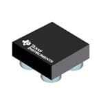
| 封装/外壳 | 4-XFBGA,DSBGA |
| 封装/箱体 | DSBGA-4 |
| 工作温度 | -40°C ~ 85°C |
| 工作电源电压 | 1.4 V to 5.5 V |
| 工厂包装数量 | 250 |
| 开关电流—最大值 | 2 A |
| 开关类型 | 通用 |
| 最大工作温度 | + 85 C |
| 最大输入电压 | 5.5 V |
| 最小工作温度 | - 40 C |
| 最小输入电压 | 1.4 V |
| 标准包装 | 250 |
| 比率-输入:输出 | 1:1 |
| 特性 | 负载释放,压摆率受控型 |
| 电压-负载 | 1.4 V ~ 5.5 V |
| 电压-输入 | 1.4 V ~ 5.5 V |
| 电流-输出(最大值) | 2A |
| 电流限制 | 2A |
| 电源电流—最大值 | 10 uA |
| 空闲时间—最大值 | 17 us |
| 类型 | 高端开关 |
| 系列 | TPS22913B |
| 输入类型 | 非反相 |
| 输出数 | 1 |
| 输出端数量 | 1 Output |
| 输出类型 | P 通道 |
| 运行时间—最大值 | 234 us |


- 商务部:美国ITC正式对集成电路等产品启动337调查
- 曝三星4nm工艺存在良率问题 高通将骁龙8 Gen1或转产台积电
- 太阳诱电将投资9.5亿元在常州建新厂生产MLCC 预计2023年完工
- 英特尔发布欧洲新工厂建设计划 深化IDM 2.0 战略
- 台积电先进制程称霸业界 有大客户加持明年业绩稳了
- 达到5530亿美元!SIA预计今年全球半导体销售额将创下新高
- 英特尔拟将自动驾驶子公司Mobileye上市 估值或超500亿美元
- 三星加码芯片和SET,合并消费电子和移动部门,撤换高东真等 CEO
- 三星电子宣布重大人事变动 还合并消费电子和移动部门
- 海关总署:前11个月进口集成电路产品价值2.52万亿元 增长14.8%


PDF Datasheet 数据手册内容提取
Product Sample & Technical Tools & Support & Folder Buy Documents Software Community TPS22910A,TPS22912C,TPS22913B,TPS22913C SLVSB49F–NOVEMBER2011–REVISEDJANUARY2015 TPS2291xx Ultra-small, Low On Resistance Load Switch With Controlled Turn-on 1 Features 3 Description • IntegratedSingleLoadSwitch The TPS22910A, TPS22912C, and TPS22913B/C 1 are small, low r load switches with controlled turn • FourPinWafer-Chip-ScalePackage(Nom) ON on. The device contains a P-channel MOSFET that – 0.9mm ×0.9mm,0.5-mmPitch,0.5-mm can operate over an input voltage range of 1.4 V to Height(YZV) 5.5 V. The switch is controlled by an on/off input • InputVoltageRange:1.4Vto5.5V (ON), which is capable of interfacing directly with low- voltageGPIOcontrolsignals. • LowON-Resistance The TPS22910A, TPS22912C, and TPS22913B/C – r =60mΩ atVIN=5V ON devices provide reverse current protection in ON and – r =61mΩ atVIN=3.3V ON OFF states. An internal reverse voltage comparator – r =74mΩ atVIN=1.8V disables the power-switch when the output voltage ON – rON =84mΩ atVIN=1.5V (VOUT) is driven higher than the input voltage (VIN), by V , to quickly (10 µs typ) stop the flow of current • 2-AMaximumContinuousSwitchCurrent RCP towards the input side of the switch. Reverse current • LowThresholdControlInput protection is always active, even when the power- • ControlledSlew-rate switch is disabled. Additionally, under-voltage lockout (UVLO) protection turns the switch off if the input • Under-VoltageLockOut voltageistoolow. • Full-TimeReverseCurrentProtection The TPS22913B/C contains a 150-Ω on-chip load • QuickOutputDischargeTransistor(TPS22913B/C resistor for quick output discharge when the switch is Devices) turnedoff. 2 Applications This family of devices have various slew rate options to avoid inrush current (see Device Comparison • NotebookComputerandUltrabook™ Table for details), are available in an ultra-small, • TabletsandSet-Top-Boxes space-saving 4-pin WCSP packages, and are • PortableIndustrial/MedicalEquipment characterized for operation over the free-air temperaturerangeof –40°Cto85°C. • PortableMediaPlayers • PointOfSalePins DeviceInformation(1) • GPSNavigationDevices PARTNUMBER PACKAGE BODYSIZE(NOM) • DigitalCameras TPS22910A • PortableInstrumentation TPS22912C DSBGA(4) 0.90mm×0.90mm • Smartphones/WirelessHandsets TPS22913B TPS22913C (1) For all available packages, see the orderable addendum at theendofthedatasheet. 4 Simplified Schematic Power VIN VOUT On-StateResistancevsInputVoltage Supply CIN CL RL 120 HI ON TPS22910A, GND −254C0C LO TTPPSS2222991132BC/C, GND 100 85C 80 ) WRon (m 60 40 20 0 0 0.5 1 1.5 2 2.5 3 3.5 4 4.5 5 5.5 6 Voltage (V) G000 1 An IMPORTANT NOTICE at the end of this data sheet addresses availability, warranty, changes, use in safety-critical applications, intellectualpropertymattersandotherimportantdisclaimers.PRODUCTIONDATA.
TPS22910A,TPS22912C,TPS22913B,TPS22913C SLVSB49F–NOVEMBER2011–REVISEDJANUARY2015 www.ti.com Table of Contents 1 Features.................................................................. 1 10 DetailedDescription........................................... 18 2 Applications........................................................... 1 10.1 Overview...............................................................18 3 Description............................................................. 1 10.2 FunctionalBlockDiagram.....................................18 4 SimplifiedSchematic............................................. 1 10.3 FeatureDescription...............................................18 10.4 DeviceFunctionalModes......................................19 5 RevisionHistory..................................................... 2 11 ApplicationandImplementation........................ 20 6 DeviceComparisonTable..................................... 3 11.1 ApplicationInformation..........................................20 7 PinConfigurationandFunctions......................... 3 11.2 TypicalApplication ...............................................20 8 Specifications......................................................... 4 12 PowerSupplyRecommendations..................... 30 8.1 AbsoluteMaximumRatings......................................4 13 Layout................................................................... 30 8.2 ESDRatings..............................................................4 13.1 LayoutGuidelines.................................................30 8.3 RecommendedOperatingConditions.......................4 13.2 LayoutExample....................................................30 8.4 ThermalInformation..................................................4 13.3 ThermalConsiderations........................................30 8.5 ElectricalCharacteristics...........................................5 14 DeviceandDocumentationSupport................. 31 8.6 SwitchingCharacteristics,Typical............................6 8.7 TypicalDCCharacteristics........................................7 14.1 RelatedLinks........................................................31 8.8 TypicalACCharacteristics,TPS22910A..................9 14.2 Trademarks...........................................................31 8.9 TypicalACCharacteristics,TPS22912C................11 14.3 ElectrostaticDischargeCaution............................31 8.10 TypicalACCharacteristics,TPS22913B..............13 14.4 Glossary................................................................31 8.11 TypicalACCharacteristics,TPS22913C..............15 15 Mechanical,Packaging,andOrderable Information........................................................... 31 9 ParameterMeasurementInformation................17 5 Revision History ChangesfromRevisionE(June2014)toRevisionF Page • Updated'ON'pindescriptioninthePinFunctionstable. ...................................................................................................... 3 ChangesfromRevisionD(May2014)toRevisionE Page • UpdatedSwitchingCharacteristicstable ............................................................................................................................... 6 • UpdatedTypicalDCCharacteristicssection.......................................................................................................................... 7 • UpdatedTimingWaveformsgraphic.................................................................................................................................... 17 • UpdatedApplicationCurvessection.................................................................................................................................... 22 ChangesfromRevisionC(May2013)toRevisionD Page • CombinedTPS22910A,TPS22912C,andTPS22913B/Cdatasheets. ................................................................................ 1 2 SubmitDocumentationFeedback Copyright©2011–2015,TexasInstrumentsIncorporated ProductFolderLinks:TPS22910A TPS22912C TPS22913B TPS22913C
TPS22910A,TPS22912C,TPS22913B,TPS22913C www.ti.com SLVSB49F–NOVEMBER2011–REVISEDJANUARY2015 6 Device Comparison Table RISETIMEat3.3V QUICKOUTPUT MAXIMUMOUTPUT DEVICE r (typ)at3.3V ENABLE ON (typ) DISCHARGE CURRENT TPS22910A 61mΩ 1µs No 2A ActiveLow TPS22912C 61mΩ 1000µs No 2A ActiveHigh TPS22913B 61mΩ 66µs Yes 2A ActiveHigh TPS22913C 61mΩ 660µs Yes 2A ActiveHigh 7 Pin Configuration and Functions YZVPACKAGE LASER MARKING BUMPVIEW VIEW Table1.PinAssignments B ON GND A VIN VOUT 2 1 PinFunctions PIN I/O DESCRIPTION NAME NO. VOUT A1 O Switchoutput VIN A2 I Switchinput,useabypasscapacitor(ceramic)toground. GND B1 – Ground ON B2 I Switchcontrolinput.Donotleavefloating Copyright©2011–2015,TexasInstrumentsIncorporated SubmitDocumentationFeedback 3 ProductFolderLinks:TPS22910A TPS22912C TPS22913B TPS22913C
TPS22910A,TPS22912C,TPS22913B,TPS22913C SLVSB49F–NOVEMBER2011–REVISEDJANUARY2015 www.ti.com 8 Specifications 8.1 Absolute Maximum Ratings MIN MAX UNIT V Inputvoltagerange –0.3 6 V IN V Outputvoltagerange –0.3 6 V OUT V Inputvoltagerange –0.3 6 V ON I Maximumcontinuousswitchcurrent 2 A MAX I Maximumpulsedswitchcurrent,pulse<300µs,2%dutycycle 2.5 A PLS T Operatingfree-airtemperaturerange –40 85 °C A T Maximumjunctiontemperature 125 °C J T Storagetemperaturerange –65 150 °C stg 8.2 ESD Ratings VALUE UNIT Human-bodymodel(HBM),perANSI/ESDA/JEDECJS-001(1) ±2000 V(ESD) Electrostaticdischarge Charged-devicemodel(CDM),perJEDECspecificationJESD22- V C101(2) ±1000 (1) JEDECdocumentJEP155statesthat500-VHBMallowssafemanufacturingwithastandardESDcontrolprocess.Manufacturingwith lessthan500-VHBMispossiblewiththenecessaryprecautions.Pinslistedas±2000Vmayactuallyhavehigherperformance. (2) JEDECdocumentJEP157statesthat250-VCDMallowssafemanufacturingwithastandardESDcontrolprocess.Manufacturingwith lessthan250-VCDMispossiblewiththenecessaryprecautions.Pinslistedas±1000Vmayactuallyhavehigherperformance. 8.3 Recommended Operating Conditions MIN MAX UNIT V Inputvoltagerange 1.4 5.5 V IN V ONvoltagerange 0 5.5 V ON V Outputvoltagerange V OUT IN V High-levelinputvoltage,ON VIN=1.4Vto5.5V 1.1 5.5 V IH VIN=3.61Vto5.5V 0.6 V V Low-levelinputvoltage,ON IL VIN=1.4Vto3.6V 0.4 V C Inputcapacitor 1(1) µF IN (1) Refertotheapplicationsection. 8.4 Thermal Information TPS22910 TPS22912 TPS22913 THERMALMETRIC(1) CSP CSP CSP UNIT 4PINS 4PINS 4PINS R Junction-to-ambientthermalresistance 189.1 189.1 189.1 θJA R Junction-to-case(top)thermalresistance 1.9 1.9 1.9 θJCtop R Junction-to-boardthermalresistance 36.8 36.8 36.8 °C/W θJB ψ Junction-to-topcharacterizationparameter 11.3 11.3 11.3 JT ψ Junction-to-boardcharacterizationparameter 36.8 36.8 36.8 JB (1) Formoreinformationabouttraditionalandnewthermalmetrics,seetheICPackageThermalMetricsapplicationreport,SPRA953. 4 SubmitDocumentationFeedback Copyright©2011–2015,TexasInstrumentsIncorporated ProductFolderLinks:TPS22910A TPS22912C TPS22913B TPS22913C
TPS22910A,TPS22912C,TPS22913B,TPS22913C www.ti.com SLVSB49F–NOVEMBER2011–REVISEDJANUARY2015 8.5 Electrical Characteristics Theelectricalcharacteristicsinthissectionapplytoalldevicesunlessotherwisenoted.ForTPS22910AV =0Vwhere ON enabledandV =V wheredisabled.ForTPS22912CandTPS22913B/CV =V whereenabledandV =0Vwhere ON IN ON IN ON disabled.V =1.4Vto5.5V,T =–40ºCto85ºC(unlessotherwisenoted) IN A PARAMETER TESTCONDITIONS T MIN TYP MAX UNIT A I =0mA,V =5.25V,V =Enabled 2 10 OUT IN ON I =0mA,V =4.2V,V =Enabled 2 7.0 OUT IN ON I Quiescentcurrent I =0mA,V =3.6V,V =Enabled Full 2 7.0 µA IN OUT IN ON I =0mA,V =2.5V,V =Enabled 0.9 5 OUT IN ON I =0mA,V =1.5V,V =Enabled 0.7 5 OUT IN ON R =1MΩ,V =5.25V,V =Disabled 1.2 10 L IN ON R =1MΩ,V =4.2V,V =Disabled 0.2 7.0 L IN ON I Offsupplycurrent R =1MΩ,V =3.6V,V =Disabled Full 0.1 7.0 µA IN(off) L IN ON R =1MΩ,V =2.5V,V =Disabled 0.1 5 L IN ON R =1MΩ,V =1.5V,V =Disabled 0.1 5 L IN ON V =0V,V =5.25V,V =Disabled 1.2 10 OUT IN ON V =0V,V =4.2V,V =Disabled 0.2 7.0 OUT IN ON I Leakagecurrent V =0V,V =3.6V,V =Disabled Full 0.1 7.0 µA IN(Leakage) OUT IN ON V =0V,V =2.5V,V =Disabled 0.1 5 OUT IN ON V =0V,V =1.5V,V =Disabled 0.1 5 OUT IN ON 25°C 60 80 V =5.25V,I =–200mA IN OUT Full 110 25°C 60 80 V =5.0V,I =–200mA IN OUT Full 110 25°C 60 80 V =4.2V,I =–200mA IN OUT Full 110 25°C 60.7 80 r On-resistance V =3.3V,I =–200mA mΩ ON IN OUT Full 110 25°C 63.4 90 V =2.5V,I =–200mA IN OUT Full 120 25°C 74.2 100 V =1.8V,I =–200mA IN OUT Full 130 25°C 83.9 120 V =1.5V,I =–200mA IN OUT Full 150 RPD(1) Outputpulldownresistance V =3.3V,I =30mA,V =0 25°C 153 200 Ω IN OUT ON V increasing,V =0V, IN ON 1.2 UVLO Undervoltagelockout IOUT=–100mA Full V V decreasing,V =0V,R =10Ω 0.50 IN ON L I ONinputleakagecurrent V =1.4Vto5.25VorGND Full 1 µA ON ON Reversecurrentvoltage TPS22910A,TPS22913B/C 44 V mV RCP threshold TPS22912C 54 Reversecurrentresponse t V =5V 10 µs DELAY delay IN Reversecurrentprotection I (leak) leakageafterreversecurrent V –V >V 25°C 0.3 µA RCP OUT IN RCP event. (1) OnlyappliestotheTPS22913B/Cdevices Copyright©2011–2015,TexasInstrumentsIncorporated SubmitDocumentationFeedback 5 ProductFolderLinks:TPS22910A TPS22912C TPS22913B TPS22913C
TPS22910A,TPS22912C,TPS22913B,TPS22913C SLVSB49F–NOVEMBER2011–REVISEDJANUARY2015 www.ti.com 8.6 Switching Characteristics, Typical PARAMETER TESTCONDITION TPS22910A TPS22912C TPS22913B TPS22913C UNIT VIN=5V,TA=25ºC(unlessotherwisenoted) tON Turn-ONtime RL=10Ω,CL=0.1µF 2 840 76 770 tOFF Turn-OFFtime RL=10Ω,CL=0.1µF 5.5 6.6 6.6 6.6 µs tR VOUTrisetime RL=10Ω,CL=0.1µF 1 912 82 838 tF VOUTfalltime RL=10Ω,CL=0.1µF 3 3 3 3 VIN=3.3V,TA=25ºC(unlessotherwisenoted) tON Turn-ONtime RL=10Ω,CL=0.1µF 2.5 1147 102 1048 tOFF Turn-OFFtime RL=10Ω,CL=0.1µF 7 8.6 8.5 8.6 µs tR VOUTrisetime RL=10Ω,CL=0.1µF 1 1030 97 980 tF VOUTfalltime RL=10Ω,CL=0.1µF 3.5 3 3 3 VIN=1.5V,TA=25ºC(unlessotherwisenoted) tON Turn-ONtime RL=10Ω,CL=0.1µF 4.5 2513 234 2344 tOFF Turn-OFFtime RL=10Ω,CL=0.1µF 16.5 17.4 17 18 µs tR VOUTrisetime RL=10Ω,CL=0.1µF 2 1970 244 1823 tF VOUTfalltime RL=10Ω,CL=0.1µF 7 6.5 6.5 6.5 6 SubmitDocumentationFeedback Copyright©2011–2015,TexasInstrumentsIncorporated ProductFolderLinks:TPS22910A TPS22912C TPS22913B TPS22913C
TPS22910A,TPS22912C,TPS22913B,TPS22913C www.ti.com SLVSB49F–NOVEMBER2011–REVISEDJANUARY2015 8.7 Typical DC Characteristics Thetypicalcharacteristicscurvesinthissectionapplytoalldevicesunlessotherwisenoted. 120 6 −40C VIN = 5.0V 25C VIN = 4.2V 85C VIN = 3.3V 100 5 VIN = 2.5V VIN = 1.8V VIN = 1.5V 80 4 ) V) Won (m 60 OUT ( 3 R V 40 2 20 1 0 0 0 0.5 1 1.5 2 2.5 3 3.5 4 4.5 5 5.5 6 0 0.2 0.4 0.6 0.8 1 1.2 1.4 Voltage (V) VON (V) G000 G000 Figure1.On-StateResistancevsInputVoltage Figure2.TPS22910AOnInputThreshold(ActiveLow) 6 3 VIN = 5.0V −40C 5.5 VIN = 4.2V 25C VIN = 3.3V 85C 5 VIN = 2.5V 2.5 VIN = 1.8V 4.5 VIN = 1.5V 4 2 VOUT (V) 23..355 IIN_Q (µA) 1.5 2 1 1.5 1 0.5 0.5 0 0 0 0.2 0.4 0.6 0.8 1 1.2 1.4 0 1 2 3 4 5 6 VON (V) Voltage (V) G000 G000 Figure3.TPS22912CandTPS22913B/COnInputThreshold Figure4.InputCurrent,QuiescentvsInputVoltage (ActiveHigh) 3000 180 −40C VIN = 1.4V 25C VIN = 1.5V 160 85C VIN = 1.8V 2500 VIN = 2.5V 140 VIN = 3.3V VIN = 4.2V VIN= 5.0V 2000 120 VIN = 5.5V A) N_Leak (n1500 WRon (m) 18000 II 1000 60 40 500 20 0 0 0 0.5 1 1.5 2 2.5 3 3.5 4 4.5 5 5.5 6 −40 −15 10 35 60 85 Voltage (V) Temperature (°C) G000 G000 Figure5.InputCurrent,LeakvsInputVoltage Figure6.On-stateResistancevsTemperature Copyright©2011–2015,TexasInstrumentsIncorporated SubmitDocumentationFeedback 7 ProductFolderLinks:TPS22910A TPS22912C TPS22913B TPS22913C
TPS22910A,TPS22912C,TPS22913B,TPS22913C SLVSB49F–NOVEMBER2011–REVISEDJANUARY2015 www.ti.com Typical DC Characteristics (continued) Thetypicalcharacteristicscurvesinthissectionapplytoalldevicesunlessotherwisenoted. 800 1 −40C 25C W) 0.9 700 85C n ( 0.8 o 600 ati 0.7 p ssi 0.6 nA) 500 wer Di 0.5 IIN_Off ( 340000 ximum Po 000...234 a M 0.1 200 0 −40−30−20−10 0 10 20 30 40 50 60 70 80 100 Ambient Temperature (°C) G001 WHITESPACE 0 0 0.5 1 1.5 2 2.5 3 3.5 4 4.5 5 5.5 6 WHITESPACE Voltage (V) G067 Figure8.AllowablePowerDissipation Figure7.InputCurrent,OffvsInputVoltage Figure9.UnderVoltageLockoutResponse Figure10.Full-TimeReverseCurrentProtection (IOUT=–100mA) (VIN=3.0V,VOUTRampupFrom3.0Vto3.3V) 8 SubmitDocumentationFeedback Copyright©2011–2015,TexasInstrumentsIncorporated ProductFolderLinks:TPS22910A TPS22912C TPS22913B TPS22913C
TPS22910A,TPS22912C,TPS22913B,TPS22913C www.ti.com SLVSB49F–NOVEMBER2011–REVISEDJANUARY2015 8.8 Typical AC Characteristics, TPS22910A 1 4 VIN =5.0V, CL = 0.1 µF, RL = 10 Ohms 0.8 3 0.6 tRise (µs) 0.4 tFall (µs) 2 1 0.2 VIN =5V, CL = 0.1 µF, RL = 10 Ohms 0 0 −40 −15 10 35 60 85 −40 −15 10 35 60 85 Temperature (°C) Temperature (°C) G000 G000 Figure11.RiseTimevsTemperature Figure12.FallTimevsTemperature 4 10 VIN =1.5V, CL = 0.1 µF, RL = 10 Ohms 9 8 3 7 6 tRise (µs) 2 tFall (µs) 45 3 1 2 1 VIN = 1.5V, CL = 0.1 µF, RL = 10 Ohms 0 0 −40 −15 10 35 60 85 −40 −15 10 35 60 85 Temperature (°C) Temperature (°C) G000 G000 Figure13.RiseTimevsTemperature Figure14.FallTimevsTemperature 4 8 VIN = 5.0V, CL = 0.1 µF, RL = 10 Ohms 3 6 µs) µs) On ( 2 Off ( 4 t t 1 2 VIN = 5.0V, CL = 0.1 µF, RL = 10 Ohms 0 0 −40 −15 10 35 60 85 −40 −15 10 35 60 85 Temperature (°C) Temperature (°C) G000 G000 Figure15.Turn-onTimevsTemperature Figure16.Turn-offTimevsTemperature Copyright©2011–2015,TexasInstrumentsIncorporated SubmitDocumentationFeedback 9 ProductFolderLinks:TPS22910A TPS22912C TPS22913B TPS22913C
TPS22910A,TPS22912C,TPS22913B,TPS22913C SLVSB49F–NOVEMBER2011–REVISEDJANUARY2015 www.ti.com Typical AC Characteristics, TPS22910A (continued) 7 25 VIN = 1.5V, CL = 0.1 µF, RL = 10 Ohms 6 20 5 15 4 µs) µs) On ( Off ( t 3 t 10 2 5 1 VIN = 1.5V, CL = 0.1 µF, RL = 10 Ohms 0 0 −40 −15 10 35 60 85 −40 −15 10 35 60 85 Temperature (°C) Temperature (°C) G000 G000 Figure17.Turn-onTimevsTemperature Figure18.Turn-offTimevsTemperature 2.5 25C −40C 85C 2.0 1.5 µs) e ( Ris t 1.0 0.5 CL = 0.1uF, RL = 10 Ohms, VON = 1.8V 0.0 0.0 0.5 1.0 1.5 2.0 2.5 3.0 3.5 4.0 4.5 5.0 5.5 6.0 Vin (V) G001 Figure19.RiseTimevsInputVoltage 10 SubmitDocumentationFeedback Copyright©2011–2015,TexasInstrumentsIncorporated ProductFolderLinks:TPS22910A TPS22912C TPS22913B TPS22913C
TPS22910A,TPS22912C,TPS22913B,TPS22913C www.ti.com SLVSB49F–NOVEMBER2011–REVISEDJANUARY2015 8.9 Typical AC Characteristics, TPS22912C 1200 4 VIN =5.0V, CL = 0.1 µF, RL = 10 Ohms 1000 3 800 tRise (µs) 600 tFall (µs) 2 400 1 200 VIN =5V, CL = 0.1 µF, RL = 10 Ohms 0 0 −40 −15 10 35 60 85 −40 −15 10 35 60 85 Temperature (°C) Temperature (°C) G000 G000 Figure20.RiseTimevsTemperature Figure21.FallTimevsTemperature 3000 10 VIN =1.5V, CL = 0.1 µF, RL = 10 Ohms 9 2500 8 7 2000 6 tRise (µs)1500 tFall (µs) 45 1000 3 2 500 1 VIN = 1.5V, CL = 0.1 µF, RL = 10 Ohms 0 0 −40 −15 10 35 60 85 −40 −15 10 35 60 85 Temperature (°C) Temperature (°C) G000 G000 Figure22.RiseTimevsTemperature Figure23.FallTimevsTemperature 1200 10 VIN = 5.0V, CL = 0.1 µF, RL = 10 Ohms 1000 8 800 6 µs) µs) On ( 600 Off ( t t 4 400 2 200 VIN = 5.0V, CL = 0.1 µF, RL = 10 Ohms 0 0 −40 −15 10 35 60 85 −40 −15 10 35 60 85 Temperature (°C) Temperature (°C) G000 G000 Figure24.Turn-onTimevsTemperature Figure25.Turn-offTimevsTemperature Copyright©2011–2015,TexasInstrumentsIncorporated SubmitDocumentationFeedback 11 ProductFolderLinks:TPS22910A TPS22912C TPS22913B TPS22913C
TPS22910A,TPS22912C,TPS22913B,TPS22913C SLVSB49F–NOVEMBER2011–REVISEDJANUARY2015 www.ti.com Typical AC Characteristics, TPS22912C (continued) 4000 25 VIN = 1.5V, CL = 0.1 µF, RL = 10 Ohms 3500 20 3000 2500 15 µs) µs) On (2000 Off ( t t 10 1500 1000 5 500 VIN = 1.5V, CL = 0.1 µF, RL = 10 Ohms 0 0 −40 −15 10 35 60 85 −40 −15 10 35 60 85 Temperature (°C) Temperature (°C) G000 G000 Figure26.Turn-onTimevsTemperature Figure27.Turn-offTimevsTemperature 3500 3000 2500 µs)2000 e ( tRis1500 1000 500 −40C 25C CL = 1 µF, RL = 10 Ohms, VON = 1.8V 85C 0 0 0.5 1 1.5 2 2.5 3 3.5 4 4.5 5 5.5 6 VIN (V) G000 Figure28.RiseTimevsInputVoltage 12 SubmitDocumentationFeedback Copyright©2011–2015,TexasInstrumentsIncorporated ProductFolderLinks:TPS22910A TPS22912C TPS22913B TPS22913C
TPS22910A,TPS22912C,TPS22913B,TPS22913C www.ti.com SLVSB49F–NOVEMBER2011–REVISEDJANUARY2015 8.10 Typical AC Characteristics, TPS22913B 180 10 VIN =5.0V, CL = 0.1 µF, RL = 10 Ohms 160 9 8 140 7 120 6 tRise (µs) 18000 tFall (µs) 45 60 3 40 2 20 1 VIN =5V, CL = 0.1 µF, RL = 10 Ohms 0 0 −40 −15 10 35 60 85 −40 −15 10 35 60 85 Temperature (°C) Temperature (°C) G000 G000 Figure29.RiseTimevsTemperature Figure30.FallTimevsTemperature 500 400 300 µs) e ( Ris t 200 100 VIN = 1.5V, CL = 0.1 µF, RL = 10 Ohms 0 −40 −15 10 35 60 85 Temperature (°C) G000 Figure31.RiseTimevsTemperature Figure32.FallTimevsTemperature 150 20 VIN = 5.0V, CL = 0.1 µF, RL = 10 Ohms 120 16 90 12 µs) µs) On ( Off ( t t 60 8 30 4 VIN = 5.0V, CL = 0.1 µF, RL = 10 Ohms 0 0 −40 −15 10 35 60 85 −40 −15 10 35 60 85 Temperature (°C) Temperature (°C) G000 G000 Figure33.Turn-onTimevsTemperature Figure34.Turn-offTimevsTemperature Copyright©2011–2015,TexasInstrumentsIncorporated SubmitDocumentationFeedback 13 ProductFolderLinks:TPS22910A TPS22912C TPS22913B TPS22913C
TPS22910A,TPS22912C,TPS22913B,TPS22913C SLVSB49F–NOVEMBER2011–REVISEDJANUARY2015 www.ti.com Typical AC Characteristics, TPS22913B (continued) 500 40 VIN = 1.5V, CL = 0.1 µF, RL = 10 Ohms 400 30 300 µs) µs) On ( Off ( 20 t t 200 10 100 VIN = 1.5V, CL = 0.1 µF, RL = 10 Ohms 0 0 −40 −15 10 35 60 85 −40 −15 10 35 60 85 Temperature (°C) Temperature (°C) G000 G000 Figure35.Turn-onTimevsTemperature Figure36.Turn-offTimevsTemperature 300 250 200 µs) e ( 150 Ris t 100 50 −40°C 25°C CL= 0.1 µF, RL= 10 Ohms, VON = 1.8V 85°C 0 0 0.5 1 1.5 2 2.5 3 3.5 4 4.5 5 5.5 6 VIN (V) G000 Figure37.RiseTimevsInputVoltage 14 SubmitDocumentationFeedback Copyright©2011–2015,TexasInstrumentsIncorporated ProductFolderLinks:TPS22910A TPS22912C TPS22913B TPS22913C
TPS22910A,TPS22912C,TPS22913B,TPS22913C www.ti.com SLVSB49F–NOVEMBER2011–REVISEDJANUARY2015 8.11 Typical AC Characteristics, TPS22913C 1200 4 VIN =5.0V, CL = 0.1 µF, RL = 10 Ohms 1000 3 800 tRise (µs) 600 tFall (µs) 2 400 1 200 VIN =5V, CL = 0.1 µF, RL = 10 Ohms 0 0 −40 −15 10 35 60 85 −40 −15 10 35 60 85 Temperature (°C) Temperature (°C) G000 G000 Figure38.RiseTimevsTemperature Figure39.FallTimevsTemperature 3000 10 VIN =1.5V, CL = 0.1 µF, RL = 10 Ohms 9 2500 8 7 2000 6 tRise (µs)1500 tFall (µs) 45 1000 3 2 500 1 VIN = 1.5V, CL = 0.1 µF, RL = 10 Ohms 0 0 −40 −15 10 35 60 85 −40 −15 10 35 60 85 Temperature (°C) Temperature (°C) G000 G000 Figure40.RiseTimevsTemperature Figure41.FallTimevsTemperature 1200 10 VIN = 5.0V, CL = 0.1 µF, RL = 10 Ohms 1000 8 800 6 µs) µs) On ( 600 Off ( t t 4 400 2 200 VIN = 5.0V, CL = 0.1 µF, RL = 10 Ohms 0 0 −40 −15 10 35 60 85 −40 −15 10 35 60 85 Temperature (°C) Temperature (°C) G000 G000 Figure42.Turn-onTimevsTemperature Figure43.Turn-OffTimevsTemperature Copyright©2011–2015,TexasInstrumentsIncorporated SubmitDocumentationFeedback 15 ProductFolderLinks:TPS22910A TPS22912C TPS22913B TPS22913C
TPS22910A,TPS22912C,TPS22913B,TPS22913C SLVSB49F–NOVEMBER2011–REVISEDJANUARY2015 www.ti.com Typical AC Characteristics, TPS22913C (continued) 3500 25 VIN = 1.5V, CL = 0.1 µF, RL = 10 Ohms 3000 20 2500 15 2000 µs) µs) On ( Off ( t1500 t 10 1000 5 500 VIN = 1.5V, CL = 0.1 µF, RL = 10 Ohms 0 0 −40 −15 10 35 60 85 −40 −15 10 35 60 85 Temperature (°C) Temperature (°C) G000 G000 Figure44.Turn-OnTimevsTemperature Figure45.Turn-OffTimevsTemperature 3000 2500 2000 µs) e (1500 Ris t 1000 500 −40°C 25°C CL= 1 µF, RL= 10 Ohms, VON = 1.8V 85°C 0 0 0.5 1 1.5 2 2.5 3 3.5 4 4.5 5 5.5 6 VIN (V) G000 Figure46.RiseTimevsInputVoltage 16 SubmitDocumentationFeedback Copyright©2011–2015,TexasInstrumentsIncorporated ProductFolderLinks:TPS22910A TPS22912C TPS22913B TPS22913C
TPS22910A,TPS22912C,TPS22913B,TPS22913C www.ti.com SLVSB49F–NOVEMBER2011–REVISEDJANUARY2015 9 Parameter Measurement Information V V IN OUT C = 1µF IN + C L - R L HI TPS22910A, ON GND (A) TPS22912C, TPS22913B/C LO GND GND Figure47. TimingTestCircuit V ON 50% 50% t t t F t OFF R ON V V OUT 90% 90% OUT 50% 50% 10% 10% A. Riseandfalltimesofthecontrolsignalis100ns. Figure48. TimingWaveforms Copyright©2011–2015,TexasInstrumentsIncorporated SubmitDocumentationFeedback 17 ProductFolderLinks:TPS22910A TPS22912C TPS22913B TPS22913C
TPS22910A,TPS22912C,TPS22913B,TPS22913C SLVSB49F–NOVEMBER2011–REVISEDJANUARY2015 www.ti.com 10 Detailed Description 10.1 Overview This family of devices are single channel, 2-A load switches in ultra-small, space saving 4-pin WCSP package. These devices implement a low resistance P-channel MOSFET with a controlled rise time for applications that needtolimittheinrushcurrent. These devices are designed to have very low leakage current during off state. This prevents downstream circuits from pulling high standby current from the supply. Integrated control logic, driver, power supply, and output discharge FET eliminates the need for additional external components, which reduces solution size and BOM count. 10.2 Functional Block Diagram VIN Reverse Current Protection Control ON Driver Logic VOUT TPS22913 only QOD GND 10.3 Feature Description 10.3.1 On/OffControl The ON pin controls the state of the switch. The ON pin is compatible with standard GPIO logic threshold. It can beusedwithanymicrocontrollerwith1.2-V,1.8-V,2.5-V,3.3-V,or5.5-VGPIO. 10.3.2 Under-VoltageLockout Under-voltage lockout protection turns off the switch if the input voltage drops below the under-voltage lockout threshold (UVLO). With the ON pin active, the input voltage rising above the under-voltage lockout threshold will causeacontrolledturn-onoftheswitchtolimitcurrentover-shoot. 18 SubmitDocumentationFeedback Copyright©2011–2015,TexasInstrumentsIncorporated ProductFolderLinks:TPS22910A TPS22912C TPS22913B TPS22913C
TPS22910A,TPS22912C,TPS22913B,TPS22913C www.ti.com SLVSB49F–NOVEMBER2011–REVISEDJANUARY2015 Feature Description (continued) 10.3.3 Full-TimeReverseCurrentProtection In a scenario where V is greater than V , there is potential for reverse current to flow through the pass FET OUT IN or the body diode. The devices monitor V and V voltage levels. When the reverse current voltage threshold IN OUT (V ) is exceeded, the switch is disabled (within 10μs typ). Additionally, the body diode is disengaged so as to RCP preventanyreversecurrentflowtoVIN.Thepeakinstantaneousreversecurrentisthecurrentittakestoactivate the reverse current protection. After the reverse current protection has activated due to the peak instantaneous reverse current, the DC (off-state) leakage current from V and V is referred to as I (leak) (see Figure 49). OUT IN RCP The pass FET, and the output voltage (V ), will resume normal operation when the reverse voltage scenario is OUT nolongerpresent. The following formula can be used to calculate the amount of peak instantaneous reverse current for a particular application: V I = RCP RC r ON(VIN) Where, I istheamountofreversecurrent, RC r istheon-resistanceattheVINofthereversecurrentcondition. ON(VIN) V isthereversevoltagethreshold. RCP V OUT V RCP I RC V IN I REVERSE_CURRENT I (leak) RCP Figure49. ReverseCurrent 10.4 Device Functional Modes Table2describeswhattheVOUTpinwillbeconnectedtoforaparticulardeviceasdeterminedbytheONpin Table2.VOUTFunctionTable ON TPS22910A TPS22912C TPS22913B/C L VIN Open GND H Open VIN VIN Copyright©2011–2015,TexasInstrumentsIncorporated SubmitDocumentationFeedback 19 ProductFolderLinks:TPS22910A TPS22912C TPS22913B TPS22913C
TPS22910A,TPS22912C,TPS22913B,TPS22913C SLVSB49F–NOVEMBER2011–REVISEDJANUARY2015 www.ti.com 11 Application and Implementation 11.1 Application Information This section will highlight some of the design considerations when implementing this device in various applications. A PSPICE model for this device is also available in the product page of this device on www.ti.com forfurtheraid. 11.1.1 VINtoVOUTVoltageDrop The VIN to VOUT voltage drop in the device is determined by the R of the device and the load current. The ON R of the device depends upon the VIN condition of the device. Refer to the R specification of the device in ON ON the Electrical Characteristics table of this datasheet. Once the R of the device is determined based upon the ON VINconditions,useEquation1tocalculatetheVINtoVOUTvoltagedrop: ΔV=I ×R (1) LOAD ON Where, ΔV=VoltagedropfromVINtoVOUT I =Loadcurrent LOAD R =On-resistanceofthedeviceforaspecificV ON IN AnappropriateI mustbechosensuchthattheI specificationofthedeviceisnotviolated. LOAD MAX 11.1.2 On/OffControl TheONpincontrolsthestateoftheswitch.TheONpinhasalowthreshold,makingitcapableofinterfacingwith low-voltage signals. The ON pin is compatible with standard GPIO logic thresholds. It can be used with any microcontroller with 1.2 V or higher GPIO voltage. This pin cannot be left floating and must be driven either high orlowforproperfunctionality. 11.1.3 InputCapacitor(Optional) To limit the voltage drop on the input supply caused by transient inrush currents when the switch turns on into a discharged load capacitor or short-circuit, a capacitor needs to be placed between V and GND. A 1-µF ceramic IN capacitor, C , placed close to the pins, is usually sufficient. Higher values of C can be used to further reduce IN IN the voltage drop during high current applications. When switching heavy loads, it is recommended to have an inputcapacitorabout10timeshigherthantheoutputcapacitortoavoidexcessivevoltagedrop. 11.1.4 OutputCapacitor(Optional) Due to the integrated body diode in the PMOS switch, a C greater than C is highly recommended. A C IN L L greater than C can cause V to exceed V when the system supply is removed. This could result in current IN OUT IN flow through the body diode from V to V . A C to C ratio of 10 to 1 is recommended for minimizing VIN dip OUT IN IN L caused by inrush currents during startup, however a 10 to 1 ratio for capacitance is not required for proper functionality of the device. A ratio smaller than 10 to 1 (such as 1 to 1) could cause slightly more V dip upon IN turn-onduetoinrushcurrents.Thiscanbemitigatedbyusingadevicewithalongerrisetime. 11.2 Typical Application Power VIN V OUT Supply C IN C R L L HI ON TPS22910A, GND LO TPS22912C, TPS22913B/C GND Figure50. TypicalApplication 20 SubmitDocumentationFeedback Copyright©2011–2015,TexasInstrumentsIncorporated ProductFolderLinks:TPS22910A TPS22912C TPS22913B TPS22913C
TPS22910A,TPS22912C,TPS22913B,TPS22913C www.ti.com SLVSB49F–NOVEMBER2011–REVISEDJANUARY2015 Typical Application (continued) 11.2.1 DesignRequirements DesignParameter ExampleValue VIN 1.5Vto5V CL 0.1µFto1µF MaximumAcceptableInrushCurrent 1A 11.2.2 DetailedDesignProcedure 11.2.2.1 InrushCurrent When the switch is enabled, the output capacitors must be charged up from 0-V to VIN voltage. This charge arrivesintheformofinrushcurrent.Inrushcurrentcanbecalculatedusingthefollowingequation: dv InrushCurrent=C´ dt (2) Where, C=Outputcapacitance dv dt =Outputslewrate The TPS22910A, TPS22912C, and TPS22913B/C offer several different rise time options to control the inrush current during turn-on. The appropriate device can be selected based upon the maximum acceptable slew rate whichcanbecalculatedusingthedesignrequirementsandtheinrushcurrentequation.Anoutputcapacitanceof 1.0 µFwillbeusedsincetheinrushfollowsthefollowingequations: dv 1.0A =1.0μF´ dt (3) dv =1V/μs dt (4) Toensureaninrushcurrentoflessthan1A,adevicewithaslewratelessthan1V/µsmustbeused The TPS22910A has a typical rise time of 1 µs at 3.3 V . This results in a slew rate of 3.3 V/µs which is above the1V/µsrequirementmeaningtheTPS22910couldnotbeusedtomeetthedesignrequirements. The TPS22913B has a typical rise time of 66 µs at 3.3 V. This results in a slew rate of 50 mV/µs which is below the 1 V/µs requirement; therefor, the TPS22913B could be used to meet the design requirements. The TPS22912C or TPS22913C have lower slew rates than the TPS22913B, so they could also be used, but the outputwouldrisemoreslowly. Copyright©2011–2015,TexasInstrumentsIncorporated SubmitDocumentationFeedback 21 ProductFolderLinks:TPS22910A TPS22912C TPS22913B TPS22913C
TPS22910A,TPS22912C,TPS22913B,TPS22913C SLVSB49F–NOVEMBER2011–REVISEDJANUARY2015 www.ti.com 11.2.3 ApplicationCurves 11.2.3.1 TypicalApplicationCharacteristicsforTPS22910A The dark blue curve (Channel 1) represents the VOUT pin of the device. The light blue curve (Channel 2) representstheONpinofthedevice. V =5V T =25°C C =10µF V =5V T =25°C C =10µF IN A IN IN A IN C =0.1µF R =10Ω C =0.1µF R =10Ω L L L L Figure51.Turn-onResponse Figure52.Turn-offResponse V =5V T =25°C C =10µF V =5V T =25°C C =10µF IN A IN IN A IN C =1µF R =10Ω C =1µF R =10Ω L L L L Figure53.Turn-onResponseTime Figure54.Turn-offResponseTime V =1.5V T =25°C C =10µF V =1.5V T =25°C C =10µF IN A IN IN A IN C =0.1µF R =10Ω C =0.1µF R =10Ω L L L L Figure55.Turn-onResponseTime Figure56.Turn-offResponseTime 22 SubmitDocumentationFeedback Copyright©2011–2015,TexasInstrumentsIncorporated ProductFolderLinks:TPS22910A TPS22912C TPS22913B TPS22913C
TPS22910A,TPS22912C,TPS22913B,TPS22913C www.ti.com SLVSB49F–NOVEMBER2011–REVISEDJANUARY2015 V =1.5V T =25°C C =10µF V =1.5V T =25°C C =10µF IN A IN IN A IN C =1µF R =10Ω C =1µF R =10Ω L L L L Figure58.Turn-offResponseTime Figure57.Turn-onResponseTime Copyright©2011–2015,TexasInstrumentsIncorporated SubmitDocumentationFeedback 23 ProductFolderLinks:TPS22910A TPS22912C TPS22913B TPS22913C
TPS22910A,TPS22912C,TPS22913B,TPS22913C SLVSB49F–NOVEMBER2011–REVISEDJANUARY2015 www.ti.com 11.2.3.2 TypicalApplicationCharacteristicsforTPS22912C The dark blue curve (Channel 1) represents the VOUT pin of the device. The light blue curve (Channel 2) representstheONpinofthedevice. V =5V T =25°C C =1µF V =5V T =25°C C =1µF IN A IN IN A IN C =0.1µF R =10Ω C =0.1µF R =10Ω L L L L Figure59.Turn-onResponse Figure60.Turn-offResponse V =5V T =25°C C =10µF V =5 T =25°C C =10µF IN A IN IN A IN C =1µF R =10Ω C =1µF R =10Ω L L L L Figure61.Turn-onResponseTime Figure62.Turn-offResponseTime V =1.5V T =25°C C =1µF V =1.5V T =25°C C =1µF IN A IN IN A IN C =0.1µF R =10Ω C =0.1µF R =10Ω L L L L Figure63.Turn-onResponseTime Figure64.Turn-offResponseTime 24 SubmitDocumentationFeedback Copyright©2011–2015,TexasInstrumentsIncorporated ProductFolderLinks:TPS22910A TPS22912C TPS22913B TPS22913C
TPS22910A,TPS22912C,TPS22913B,TPS22913C www.ti.com SLVSB49F–NOVEMBER2011–REVISEDJANUARY2015 V =1.5V T =25°C C =10µF V =1.5V T =25°C C =10µF IN A IN IN A IN C =1µF R =10Ω C =1µF R =10Ω L L L L Figure65.Turn-onResponseTime Figure66.Turn-offResponseTime Copyright©2011–2015,TexasInstrumentsIncorporated SubmitDocumentationFeedback 25 ProductFolderLinks:TPS22910A TPS22912C TPS22913B TPS22913C
TPS22910A,TPS22912C,TPS22913B,TPS22913C SLVSB49F–NOVEMBER2011–REVISEDJANUARY2015 www.ti.com 11.2.3.3 TypicalApplicationCharacteristicsForTPS22913B The dark blue curve (Channel 1) represents the VOUT pin of the device. The light blue curve (Channel 2) representstheONpinofthedevice. V =5V T =25°C C =10µF V =5V T =25°C C =10µF IN A IN IN A IN C =1µF R =10Ω C =1µF R =10Ω L L L L Figure67.Turn-onResponse Figure68.Turn-offResponse V =5V T =25°C C =1µF V =5V T =25°C C =1µF IN A IN IN A IN C =0.1µF R =10Ω C =0.1µF R =10Ω L L L L Figure69.Turn-onResponseTime Figure70.Turn-offResponseTime V =1.5V T =25°C C =10µF V =1.5V T =25°C C =10µF IN A IN IN A IN C =1µF R =10Ω C =1µF R =10Ω L L L L Figure71.Turn-onResponseTime Figure72.Turn-offResponseTime 26 SubmitDocumentationFeedback Copyright©2011–2015,TexasInstrumentsIncorporated ProductFolderLinks:TPS22910A TPS22912C TPS22913B TPS22913C
TPS22910A,TPS22912C,TPS22913B,TPS22913C www.ti.com SLVSB49F–NOVEMBER2011–REVISEDJANUARY2015 V =1.5V T =25°C C =1µF V =1.5V T =25°C C =1µF IN A IN IN A IN C =0.1µF R =10Ω C =0.1µF R =10Ω L L L L Figure73.Turn-onResponseTime Figure74.Turn-offResponseTime Copyright©2011–2015,TexasInstrumentsIncorporated SubmitDocumentationFeedback 27 ProductFolderLinks:TPS22910A TPS22912C TPS22913B TPS22913C
TPS22910A,TPS22912C,TPS22913B,TPS22913C SLVSB49F–NOVEMBER2011–REVISEDJANUARY2015 www.ti.com 11.2.3.4 TypicalApplicationCharacteristicsforTPS22913C The dark blue curve (Channel 1) represents the VOUT pin of the device. The light blue curve (Channel 2) representstheONpinofthedevice. V =5V T =25°C C =10µF V =5V T =25°C C =10µF IN A IN IN A IN C =1µF R =10Ω C =1µF R =10Ω L L L L Figure75.Turn-OnResponseTime Figure76.Turn-OffResponseTime V =5V T =25°C C =1µF V =5V T =25°C C =1µF IN A IN IN A IN C =0.1µF R =10Ω C =0.1µF R =10Ω L L L L Figure77.Turn-OnResponseTime Figure78.Turn-OffResponseTime V =1.5V T =25°C C =10µF V =1.5V T =25°C C =10µF IN A IN IN A IN C =1µF R =10Ω C =1µF R =10Ω L L L L Figure79.Turn-OffResponseTime Figure80.Turn-OffResponseTime 28 SubmitDocumentationFeedback Copyright©2011–2015,TexasInstrumentsIncorporated ProductFolderLinks:TPS22910A TPS22912C TPS22913B TPS22913C
TPS22910A,TPS22912C,TPS22913B,TPS22913C www.ti.com SLVSB49F–NOVEMBER2011–REVISEDJANUARY2015 V =1.5V T =25°C C =1µF V =1.5V T =25°C C =1µF IN A IN IN A IN C =0.1µF R =10Ω C =0.1µF R =10Ω L L L L Figure81.Turn-OffResponseTime Figure82.Turn-OffResponseTime Copyright©2011–2015,TexasInstrumentsIncorporated SubmitDocumentationFeedback 29 ProductFolderLinks:TPS22910A TPS22912C TPS22913B TPS22913C
TPS22910A,TPS22912C,TPS22913B,TPS22913C SLVSB49F–NOVEMBER2011–REVISEDJANUARY2015 www.ti.com 12 Power Supply Recommendations ThedeviceisdesignedtooperatewithaVINrangeof1.4Vto5.5V. 13 Layout 13.1 Layout Guidelines For best performance, all traces should be as short as possible. To be most effective, the input and output capacitors should be placed close to the device to minimize the effects that parasitic trace inductances may have on normal operation. Using wide traces for VIN, VOUT, and GND helps minimize the parasitic electrical effects alongwithminimizingthecasetoambientthermalimpedance. 13.2 Layout Example The figure below shows an example for these devices. Notice the connection to system ground between the V Bypass Capacitor ground and the GND pin of the load switch, this creates a ground barrier which helps to OUT reducethegroundnoiseseenbythedevice. To GPIO control GND Gnd Via ON B2 B1 Gnd VINBypass Via VOUTBypass Capacitor Capacitor VIN A2 A1 VOUT VIAto Power Ground Plane 13.3 Thermal Considerations The maximum IC junction temperature should be restricted to 125°C under normal operating conditions. To calculate the maximum allowable dissipation, P for a given output current and ambient temperature, use the D(max) followingequationasaguideline: T -T P = J(MAX) A D(MAX) R θJA (5) where • P =maximumallowablepowerdissipation D(max) • T =maximumallowablejunctiontemperature J(max) • T =ambienttemperatureofthedevice A • θ = junction to air thermal impedance. See the Thermal Information section. This parameter is highly JA dependentuponboardlayout. 30 SubmitDocumentationFeedback Copyright©2011–2015,TexasInstrumentsIncorporated ProductFolderLinks:TPS22910A TPS22912C TPS22913B TPS22913C
TPS22910A,TPS22912C,TPS22913B,TPS22913C www.ti.com SLVSB49F–NOVEMBER2011–REVISEDJANUARY2015 14 Device and Documentation Support 14.1 Related Links The table below lists quick access links. Categories include technical documents, support and community resources,toolsandsoftware,andquickaccesstosampleorbuy. Table3.RelatedLinks TECHNICAL TOOLS& SUPPORT& PARTS PRODUCTFOLDER SAMPLE&BUY DOCUMENTS SOFTWARE COMMUNITY TPS22910A Clickhere Clickhere Clickhere Clickhere Clickhere TPS22912C Clickhere Clickhere Clickhere Clickhere Clickhere TPS22913B Clickhere Clickhere Clickhere Clickhere Clickhere TPS22913C Clickhere Clickhere Clickhere Clickhere Clickhere 14.2 Trademarks UltrabookisatrademarkofIntel. Allothertrademarksarethepropertyoftheirrespectiveowners. 14.3 Electrostatic Discharge Caution Thesedeviceshavelimitedbuilt-inESDprotection.Theleadsshouldbeshortedtogetherorthedeviceplacedinconductivefoam duringstorageorhandlingtopreventelectrostaticdamagetotheMOSgates. 14.4 Glossary SLYZ022—TIGlossary. Thisglossarylistsandexplainsterms,acronyms,anddefinitions. 15 Mechanical, Packaging, and Orderable Information The following pages include mechanical, packaging, and orderable information. This information is the most current data available for the designated devices. This data is subject to change without notice and revision of thisdocument.Forbrowser-basedversionsofthisdatasheet,refertotheleft-handnavigation. Copyright©2011–2015,TexasInstrumentsIncorporated SubmitDocumentationFeedback 31 ProductFolderLinks:TPS22910A TPS22912C TPS22913B TPS22913C
PACKAGE OPTION ADDENDUM www.ti.com 1-Dec-2015 PACKAGING INFORMATION Orderable Device Status Package Type Package Pins Package Eco Plan Lead/Ball Finish MSL Peak Temp Op Temp (°C) Device Marking Samples (1) Drawing Qty (2) (6) (3) (4/5) TPS22910AYZVR ACTIVE DSBGA YZV 4 3000 Green (RoHS SNAGCU Level-1-260C-UNLIM -40 to 85 75 & no Sb/Br) TPS22910AYZVT ACTIVE DSBGA YZV 4 250 Green (RoHS SNAGCU Level-1-260C-UNLIM -40 to 85 75 & no Sb/Br) TPS22912CYZVR ACTIVE DSBGA YZV 4 3000 Green (RoHS SNAGCU Level-1-260C-UNLIM -40 to 85 78 & no Sb/Br) TPS22912CYZVT ACTIVE DSBGA YZV 4 250 Green (RoHS SNAGCU Level-1-260C-UNLIM -40 to 85 78 & no Sb/Br) TPS22913BYZVR ACTIVE DSBGA YZV 4 3000 Green (RoHS SNAGCU Level-1-260C-UNLIM -40 to 85 64 & no Sb/Br) TPS22913BYZVT ACTIVE DSBGA YZV 4 250 Green (RoHS SNAGCU Level-1-260C-UNLIM -40 to 85 64 & no Sb/Br) TPS22913CYZVR ACTIVE DSBGA YZV 4 3000 Green (RoHS SNAGCU Level-1-260C-UNLIM -40 to 85 76 & no Sb/Br) TPS22913CYZVT ACTIVE DSBGA YZV 4 250 Green (RoHS SNAGCU Level-1-260C-UNLIM -40 to 85 76 & no Sb/Br) (1) The marketing status values are defined as follows: ACTIVE: Product device recommended for new designs. LIFEBUY: TI has announced that the device will be discontinued, and a lifetime-buy period is in effect. NRND: Not recommended for new designs. Device is in production to support existing customers, but TI does not recommend using this part in a new design. PREVIEW: Device has been announced but is not in production. Samples may or may not be available. OBSOLETE: TI has discontinued the production of the device. (2) Eco Plan - The planned eco-friendly classification: Pb-Free (RoHS), Pb-Free (RoHS Exempt), or Green (RoHS & no Sb/Br) - please check http://www.ti.com/productcontent for the latest availability information and additional product content details. TBD: The Pb-Free/Green conversion plan has not been defined. Pb-Free (RoHS): TI's terms "Lead-Free" or "Pb-Free" mean semiconductor products that are compatible with the current RoHS requirements for all 6 substances, including the requirement that lead not exceed 0.1% by weight in homogeneous materials. Where designed to be soldered at high temperatures, TI Pb-Free products are suitable for use in specified lead-free processes. Pb-Free (RoHS Exempt): This component has a RoHS exemption for either 1) lead-based flip-chip solder bumps used between the die and package, or 2) lead-based die adhesive used between the die and leadframe. The component is otherwise considered Pb-Free (RoHS compatible) as defined above. Green (RoHS & no Sb/Br): TI defines "Green" to mean Pb-Free (RoHS compatible), and free of Bromine (Br) and Antimony (Sb) based flame retardants (Br or Sb do not exceed 0.1% by weight in homogeneous material) (3) MSL, Peak Temp. - The Moisture Sensitivity Level rating according to the JEDEC industry standard classifications, and peak solder temperature. Addendum-Page 1
PACKAGE OPTION ADDENDUM www.ti.com 1-Dec-2015 (4) There may be additional marking, which relates to the logo, the lot trace code information, or the environmental category on the device. (5) Multiple Device Markings will be inside parentheses. Only one Device Marking contained in parentheses and separated by a "~" will appear on a device. If a line is indented then it is a continuation of the previous line and the two combined represent the entire Device Marking for that device. (6) Lead/Ball Finish - Orderable Devices may have multiple material finish options. Finish options are separated by a vertical ruled line. Lead/Ball Finish values may wrap to two lines if the finish value exceeds the maximum column width. Important Information and Disclaimer:The information provided on this page represents TI's knowledge and belief as of the date that it is provided. TI bases its knowledge and belief on information provided by third parties, and makes no representation or warranty as to the accuracy of such information. Efforts are underway to better integrate information from third parties. TI has taken and continues to take reasonable steps to provide representative and accurate information but may not have conducted destructive testing or chemical analysis on incoming materials and chemicals. TI and TI suppliers consider certain information to be proprietary, and thus CAS numbers and other limited information may not be available for release. In no event shall TI's liability arising out of such information exceed the total purchase price of the TI part(s) at issue in this document sold by TI to Customer on an annual basis. Addendum-Page 2
PACKAGE MATERIALS INFORMATION www.ti.com 25-May-2019 TAPE AND REEL INFORMATION *Alldimensionsarenominal Device Package Package Pins SPQ Reel Reel A0 B0 K0 P1 W Pin1 Type Drawing Diameter Width (mm) (mm) (mm) (mm) (mm) Quadrant (mm) W1(mm) TPS22910AYZVR DSBGA YZV 4 3000 178.0 9.2 1.0 1.0 0.63 4.0 8.0 Q1 TPS22910AYZVT DSBGA YZV 4 250 178.0 9.2 1.0 1.0 0.63 4.0 8.0 Q1 TPS22912CYZVR DSBGA YZV 4 3000 178.0 9.2 1.0 1.0 0.63 4.0 8.0 Q1 TPS22912CYZVT DSBGA YZV 4 250 178.0 9.2 1.0 1.0 0.63 4.0 8.0 Q1 TPS22913BYZVR DSBGA YZV 4 3000 180.0 8.4 1.0 1.0 0.63 4.0 8.0 Q1 TPS22913BYZVR DSBGA YZV 4 3000 178.0 9.2 1.0 1.0 0.63 4.0 8.0 Q1 TPS22913BYZVT DSBGA YZV 4 250 178.0 9.2 1.0 1.0 0.63 4.0 8.0 Q1 TPS22913CYZVR DSBGA YZV 4 3000 178.0 9.2 1.0 1.0 0.63 4.0 8.0 Q1 TPS22913CYZVT DSBGA YZV 4 250 178.0 9.2 1.0 1.0 0.63 4.0 8.0 Q1 PackMaterials-Page1
PACKAGE MATERIALS INFORMATION www.ti.com 25-May-2019 *Alldimensionsarenominal Device PackageType PackageDrawing Pins SPQ Length(mm) Width(mm) Height(mm) TPS22910AYZVR DSBGA YZV 4 3000 220.0 220.0 35.0 TPS22910AYZVT DSBGA YZV 4 250 220.0 220.0 35.0 TPS22912CYZVR DSBGA YZV 4 3000 220.0 220.0 35.0 TPS22912CYZVT DSBGA YZV 4 250 220.0 220.0 35.0 TPS22913BYZVR DSBGA YZV 4 3000 182.0 182.0 20.0 TPS22913BYZVR DSBGA YZV 4 3000 220.0 220.0 35.0 TPS22913BYZVT DSBGA YZV 4 250 220.0 220.0 35.0 TPS22913CYZVR DSBGA YZV 4 3000 220.0 220.0 35.0 TPS22913CYZVT DSBGA YZV 4 250 220.0 220.0 35.0 PackMaterials-Page2
D: Max = 0.918 mm, Min =0 .858 mm E: Max = 0.918 mm, Min =0 .858 mm
IMPORTANTNOTICEANDDISCLAIMER TIPROVIDESTECHNICALANDRELIABILITYDATA(INCLUDINGDATASHEETS),DESIGNRESOURCES(INCLUDINGREFERENCE DESIGNS),APPLICATIONOROTHERDESIGNADVICE,WEBTOOLS,SAFETYINFORMATION,ANDOTHERRESOURCES“ASIS” ANDWITHALLFAULTS,ANDDISCLAIMSALLWARRANTIES,EXPRESSANDIMPLIED,INCLUDINGWITHOUTLIMITATIONANY IMPLIEDWARRANTIESOFMERCHANTABILITY,FITNESSFORAPARTICULARPURPOSEORNON-INFRINGEMENTOFTHIRD PARTYINTELLECTUALPROPERTYRIGHTS. TheseresourcesareintendedforskilleddevelopersdesigningwithTIproducts.Youaresolelyresponsiblefor(1)selectingtheappropriate TIproductsforyourapplication,(2)designing,validatingandtestingyourapplication,and(3)ensuringyourapplicationmeetsapplicable standards,andanyothersafety,security,orotherrequirements.Theseresourcesaresubjecttochangewithoutnotice.TIgrantsyou permissiontousetheseresourcesonlyfordevelopmentofanapplicationthatusestheTIproductsdescribedintheresource.Other reproductionanddisplayoftheseresourcesisprohibited.NolicenseisgrantedtoanyotherTIintellectualpropertyrightortoanythird partyintellectualpropertyright.TIdisclaimsresponsibilityfor,andyouwillfullyindemnifyTIanditsrepresentativesagainst,anyclaims, damages,costs,losses,andliabilitiesarisingoutofyouruseoftheseresources. TI’sproductsareprovidedsubjecttoTI’sTermsofSale(www.ti.com/legal/termsofsale.html)orotherapplicabletermsavailableeitheron ti.comorprovidedinconjunctionwithsuchTIproducts.TI’sprovisionoftheseresourcesdoesnotexpandorotherwisealterTI’sapplicable warrantiesorwarrantydisclaimersforTIproducts. MailingAddress:TexasInstruments,PostOfficeBox655303,Dallas,Texas75265 Copyright©2019,TexasInstrumentsIncorporated