ICGOO在线商城 > 集成电路(IC) > PMIC - 配电开关,负载驱动器 > NUD3160LT1G
 Datasheet下载
- 型号: NUD3160LT1G
- 制造商: ON Semiconductor
- 库位|库存: xxxx|xxxx
- 要求:
| 数量阶梯 | 香港交货 | 国内含税 |
| +xxxx | $xxxx | ¥xxxx |
查看当月历史价格
查看今年历史价格
NUD3160LT1G产品简介:
ICGOO电子元器件商城为您提供NUD3160LT1G由ON Semiconductor设计生产,在icgoo商城现货销售,并且可以通过原厂、代理商等渠道进行代购。 NUD3160LT1G价格参考¥1.06-¥1.06。ON SemiconductorNUD3160LT1G封装/规格:PMIC - 配电开关,负载驱动器, Power Switch/Driver 1:1 N-Channel 150mA SOT-23-3 (TO-236)。您可以下载NUD3160LT1G参考资料、Datasheet数据手册功能说明书,资料中有NUD3160LT1G 详细功能的应用电路图电压和使用方法及教程。
NUD3160LT1G是安森美(ON Semiconductor)推出的一款专用LED驱动和负载驱动器,属于PMIC中的配电开关类别。该器件主要用于驱动LED负载,特别适用于需要简单、高效、低成本解决方案的中小功率LED应用。

典型应用场景包括:汽车内部照明,如仪表盘背光、车门灯、氛围灯、阅读灯等;消费类电子产品中的LED指示灯或背光源;工业控制面板的信号指示灯;以及家电产品中的状态显示照明。NUD3160LT1G具备恒流输出特性,可确保LED亮度稳定,避免因电源波动导致的闪烁或损坏。

该器件采用小型表面贴装封装(SOT-223),集成度高,无需外接复杂元件,节省电路板空间。其内置过温保护功能,提升了系统可靠性。此外,它支持宽电压输入范围,适用于12V或24V直流系统,尤其适合汽车电子环境。

由于其具备使能控制端(EN),可通过微控制器实现LED的开关调光,便于系统进行智能控制。总体而言,NUD3160LT1G是一款专为LED照明优化的高性价比负载驱动器,广泛应用于对空间、成本和可靠性有要求的中低功率LED驱动场景。
| 参数 | 数值 |
| 产品目录 | 集成电路 (IC)半导体 |
| ChannelMode | Enhancement |
| 描述 | IC INDCT LOAD DRVR INDUST SOT23MOSFET 61V Industrial Load Driver |
| 产品分类 | PMIC - MOSFET,电桥驱动器 - 内部开关分离式半导体 |
| Id-ContinuousDrainCurrent | 150 mA |
| Id-连续漏极电流 | 150 mA |
| 品牌 | ON Semiconductor |
| 产品手册 | |
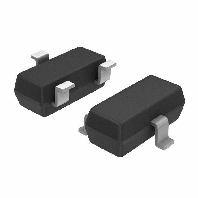
| 产品图片 |
|
| rohs | 符合RoHS无铅 / 符合限制有害物质指令(RoHS)规范要求 |
| 产品系列 | 晶体管,MOSFET,ON Semiconductor NUD3160LT1GMicroIntegration™ |
| 数据手册 | |
| 产品型号 | NUD3160LT1G |
| Pd-PowerDissipation | 225 mW |
| Pd-功率耗散 | 225 mW |
| RdsOn-Drain-SourceResistance | 1800 mOhms at 5 V |
| RdsOn-漏源导通电阻 | 1.8 Ohms |
| Vds-Drain-SourceBreakdownVoltage | 60 V |
| Vds-漏源极击穿电压 | 60 V |
| Vgs-Gate-SourceBreakdownVoltage | 12 V |
| Vgs-栅源极击穿电压 | 12 V |
| 上升时间 | 618 ns, 600 ns |
| 下降时间 | 618 ns, 600 ns |
| 产品目录页面 | |
| 产品种类 | MOSFET |
| 供应商器件封装 | SOT-23-3(TO-236) |
| 其它名称 | NUD3160LT1GOSCT |
| 功率耗散 | 225 mW |
| 包装 | 剪切带 (CT) |
| 商标 | ON Semiconductor |
| 安装类型 | 表面贴装 |
| 安装风格 | SMD/SMT |
| 导通电阻 | 2.4 欧姆 |
| 封装 | Reel |
| 封装/外壳 | TO-236-3,SC-59,SOT-23-3 |
| 封装/箱体 | SOT-23-3 |
| 工作温度 | -40°C ~ 125°C |
| 工厂包装数量 | 3000 |
| 晶体管极性 | N-Channel |
| 最大工作温度 | + 125 C |
| 最小工作温度 | - 40 C |
| 标准包装 | 1 |
| 汲极/源极击穿电压 | 60 V |
| 漏极连续电流 | 150 mA |
| 电压-电源 | 60V |
| 电流-峰值输出 | - |
| 电流-输出/通道 | 200mA |
| 类型 | 低端 |
| 系列 | NUD3160 |
| 输入类型 | 非反相 |
| 输出数 | 1 |
| 通道模式 | Enhancement |
| 配置 | Single |
| 闸/源击穿电压 | 12 V |


- 商务部:美国ITC正式对集成电路等产品启动337调查
- 曝三星4nm工艺存在良率问题 高通将骁龙8 Gen1或转产台积电
- 太阳诱电将投资9.5亿元在常州建新厂生产MLCC 预计2023年完工
- 英特尔发布欧洲新工厂建设计划 深化IDM 2.0 战略
- 台积电先进制程称霸业界 有大客户加持明年业绩稳了
- 达到5530亿美元!SIA预计今年全球半导体销售额将创下新高
- 英特尔拟将自动驾驶子公司Mobileye上市 估值或超500亿美元
- 三星加码芯片和SET,合并消费电子和移动部门,撤换高东真等 CEO
- 三星电子宣布重大人事变动 还合并消费电子和移动部门
- 海关总署:前11个月进口集成电路产品价值2.52万亿元 增长14.8%


PDF Datasheet 数据手册内容提取
NUD3160, SZNUD3160 Industrial Inductive Load Driver This micro−integrated part provides a single component solution to switch inductive loads such as relays, solenoids, and small DC motors without the need of a free−wheeling diode. It accepts logic level inputs, thus allowing it to be driven by a large variety of devices www.onsemi.com including logic gates, inverters, and microcontrollers. MARKING DIAGRAMS Features • 3 SOT−23 Provides Robust Interface between D.C. Relay Coils and Sensitive JW8 M(cid:2) CASE 318 1 (cid:2) Logic STYLE 21 2 • Capable of Driving Relay Coils Rated up to 150 mA at 12 V, 24 V or 48 V JW8 = Specific Device Code • M = Date Code Replaces 3 or 4 Discrete Components for Lower Cost (cid:2) = Pb−Free Package • Internal Zener Eliminates Need for Free−Wheeling Diode (Note: Microdot may be in either location) • Meets Load Dump and other Automotive Specs • SZ Prefix for Automotive and Other Applications Requiring Unique SC−74 JW8 M(cid:2) Site and Control Change Requirements; AEC−Q101 Qualified and 6 CASE 318F (cid:2) STYLE 7 1 PPAP Capable • These are Pb−Free Devices JW8 = Specific Device Code M = Date Code Typical Applications (cid:2) = Pb−Free Package • (Note: Microdot may be in either location) Automotive and Industrial Environment • Drives Window, Latch, Door, and Antenna Relays ORDERING INFORMATION Device Package Shipping† Benefits • NUD3160LT1G SOT−23 3000 / Tape & Reduced PCB Space (Pb−Free) Reel • Standardized Driver for Wide Range of Relays SZNUD3160LT1G SOT−23 3000 / Tape & • Simplifies Circuit Design and PCB Layout (Pb−Free) Reel • Compliance with Automotive Specifications NUD3160DMT1G SC−74 3000 / Tape & (Pb−Free) Reel SZNUD3160DMT1G SC−74 3000 / Tape & (Pb−Free) Reel †For information on tape and reel specifications, including part orientation and tape sizes, please refer to our Tape and Reel Packaging Specification Brochure, BRD8011/D. Drain (3) Drain (6) Drain (3) Gate (1) 10 k Gate (2) 10 k 10 k Gate (5) 100 k 100 k 100 k Source (2) Source (1) Source (4) CASE 318 CASE 318F Figure 1. Internal Circuit Diagrams © Semiconductor Components Industries, LLC, 2003 1 Publication Order Number: October, 2016 − Rev. 7 NUD3160/D
NUD3160, SZNUD3160 MAXIMUM RATINGS (TJ = 25°C unless otherwise specified) Symbol Rating Value Unit VDSS Drain−to−Source Voltage – Continuous (TJ = 125°C) 60 V VGSS Gate−to−Source Voltage – Continuous (TJ = 125°C) 12 V ID Drain Current – Continuous (TJ = 125°C) mA Minimum copper, double sided board, TA = 80°C SOT−23 158 157 SC74 Single device driven 132 ea SC74 Both devices driven 1 in2 copper, double sided board, TA = 25°C SOT−23 272 SC74 Single device driven 263 SC74 Both devices driven 230 ea EZ Single Pulse Drain−to−Source Avalanche Energy 200 mJ (For Relay’s Coils/Inductive Loads of 80 (cid:2) or Higher) (TJ Initial = 85°C) PPK Peak Power Dissipation, Drain−to−Source (Notes 1 and 2) 20 W (TJ Initial = 85°C) ELD1 Load Dump Pulse, Drain−to−Source (Note 3) 60 V RSOURCE = 0.5 (cid:2), T = 300 ms) (For Relay’s Coils/Inductive Loads of 80 (cid:2) or Higher) (TJ Initial = 85°C) ELD2 Inductive Switching Transient 1, Drain−to−Source 100 V (Waveform: RSOURCE = 10 (cid:2), T = 2.0 ms) (For Relay’s Coils/Inductive Loads of 80 (cid:2) or Higher) (TJ Initial = 85°C) ELD3 Inductive Switching Transient 2, Drain−to−Source 300 V (Waveform: RSOURCE = 4.0 (cid:2), T = 50 (cid:3)s) (For Relay’s Coils/Inductive Loads of 80 (cid:2) or Higher) (TJ Initial = 85°C) Rev−Bat Reverse Battery, 10 Minutes (Drain−to−Source) −14 V (For Relay’s Coils/Inductive Loads of 80 (cid:2) or more) Dual−Volt Dual Voltage Jump Start, 10 Minutes (Drain−to−Source) 28 V ESD Human Body Model (HBM) 2000 V According to EIA/JESD22/A114 Specification Stresses exceeding those listed in the Maximum Ratings table may damage the device. If any of these limits are exceeded, device functionality should not be assumed, damage may occur and reliability may be affected. www.onsemi.com 2
NUD3160, SZNUD3160 THERMAL CHARACTERISTICS Symbol Rating Value Unit TA Operating Ambient Temperature −40 to 125 °C TJ Maximum Junction Temperature 150 °C TSTG Storage Temperature Range −65 to 150 °C PD Total Power Dissipation (Note 4) SOT−23 225 mW Derating above 25°C 1.8 mW/°C PD Total Power Dissipation (Note 4) SC−74 380 mW Derating above 25°C 3.0 mW/°C R(cid:4)JA Thermal Resistance, Junction–to–Ambient °C/W Minimum Copper SOT−23 556 SC−74 One Device Powered 556 SC−74 Both Devices Equally Powered 398 300 mm2 Copper SOT−23 395 SC−74 One Device Powered 420 SC−74 Both Devices Equally Powered 270 1. Nonrepetitive current square pulse 1.0 ms duration. 2. For different square pulse durations, see Figure 12. 3. Nonrepetitive load dump pulse per Figure 3. 4. Mounted onto minimum pad board. www.onsemi.com 3
NUD3160, SZNUD3160 ELECTRICAL CHARACTERISTICS (TJ = 25°C unless otherwise specified) Characteristic Symbol Min Typ Max Unit OFF CHARACTERISTICS Drain to Source Sustaining Voltage VBRDSS 61 66 70 V (ID = 10 mA) Drain to Source Leakage Current IDSS (cid:3)A (VDS = 12 V, VGS = 0 V) − − 0.5 (VDS = 12 V, VGS = 0 V, TJ = 125°C) − − 1.0 − − 50 ((VVDDSS == 6600 VV,, VVGGSS == 00 VV,) TJ = 125°C) − − 80 Gate Body Leakage Current IGSS (cid:3)A (VGS = 3.0 V, VDS = 0 V) − − 60 (VGS = 3.0 V, VDS = 0 V, TJ = 125°C) − − 80 − − 90 ((VVGGSS == 55..00 VV,, VVDDSS == 00 VV,) TJ = 125°C) − − 110 ON CHARACTERISTICS Gate Threshold Voltage VGS(th) V (VGS = VDS, ID = 1.0 mA) 1.3 1.8 2.0 (VGS = VDS, ID = 1.0 mA, TJ = 125°C) 1.3 − 2.0 Drain to Source On−Resistance RDS(on) (cid:2) (ID = 150 mA, VGS = 3.0 V) − − 2.4 (ID = 150 mA, VGS = 3.0 V, TJ = 125°C) − − 3.7 − − 1.8 ((IIDD == 115500 mmAA,, VVGGSS == 55..00 VV,) TJ = 125°C) − − 2.9 Output Continuous Current IDS(on) mA (VDS = 0.3 V, VGS = 5.0 V) 150 200 − (VDS = 0.3 V, VGS = 5.0 V, TJ = 125°C) 100 − − Forward Transconductance gFS − 400 − mmho (VDS = 12 V, ID = 150 mA) DYNAMIC CHARACTERISTICS Input Capacitance Ciss − 30 − pf (VDS = 12 V, VGS = 0 V, f = 10 kHz) Output Capacitance Coss − 14 − pf (VDS = 12 V, VGS = 0 V, f = 10 kHz) Transfer Capacitance Crss − 6.0 − pf (VDS = 12 V, VGS = 0 V, f = 10 kHz) SWITCHING CHARACTERISTICS Propagation Delay Times: ns High to Low Propagation Delay; Figure 2, (VDS = 12 V, VGS = 3.0 V) tPHL − 918 − Low to High Propagation Delay; Figure 2, (VDS = 12 V, VGS = 3.0 V) tPLH − 798 − HLoigwh ttoo HLiogwh PPrrooppaaggaattiioonn DDeellaayy;; FFiigguurree 22,, ((VVDDSS == 1122 VV,, VVGGSS == 55..00 VV)) ttPPHLHL −− 1313610 −− Transition Times: ns Fall Time; Figure 2, (VDS = 12 V, VGS = 3.0 V) tf − 2290 − Rise Time; Figure 2, (VDS = 12 V, VGS = 3.0 V) tr − 618 − FRaislle T Timimee; ;F Figiguurere 2 2, ,( V(VDDSS = = 1 122 V V, ,V VGGSS = = 5 5.0.0 V V)) ttrf −− 662020 −− Product parametric performance is indicated in the Electrical Characteristics for the listed test conditions, unless otherwise noted. Product performance may not be indicated by the Electrical Characteristics if operated under different conditions. www.onsemi.com 4
NUD3160, SZNUD3160 TYPICAL WAVEFORMS (TJ = 25°C unless otherwise specified) VIH Vin 50% 0 V tPHL tPLH 90% VOH Vout 50% 10% VOL tf tr Figure 2. Switching Waveforms tr Load Dump Pulse Not Suppressed: 90% Vr = 13.5 V Nominal ±10% VT S= =3 0600 mV sN Nomominianla ±l 1±01%0% 10% of Peak; VS tr = 1 − 10 ms ±10% Reference = Vr, Ir 10% T Vr, Ir Figure 3. Load Dump Waveform Definition www.onsemi.com 5
NUD3160, SZNUD3160 TYPICAL PERFORMANCE CURVES (TJ = 25°C unless otherwise specified) 80 80 VDS = 60 V 70 (cid:3)A) A) 70 KAGE ( 5600 (cid:3)AGE ( 60 EA AK VGS = 5 V L 40 E 50 AIN 30 TE L DR GA 40 I, DSS1200 I GSS 30 VGS = 3 V 0 20 −50 −25 0 25 50 75 100 125 −50 −25 0 25 50 75 100 125 TJ, JUNCTION TEMPERATURE (°C) TJ, JUNCTION TEMPERATURE (°C) Figure 4. Drain−to−Source Leakage vs. Figure 5. Gate−to−Source Leakage vs. Junction Temperature Junction Temperature 66.4 1E+03 V) VGS = 5 V VGS = 3 V VGS = 2.5 V AGE ( 6666..02 mA)1E+02 VGS = 2 V OLT ID = 10 mA NT (1E+01 V 65.8 E N R W R 65.6 U1E+00 O C EAKD 65.4 RAIN 1E−01 VGS = 1.5 V R D BSS65.2 I D1E−02 D65.0 V B 64.8 1E−03 −50 −25 0 25 50 75 100 125 0.0 0.1 0.2 0.3 0.4 0.5 0.6 0.7 0.8 TJ, JUNCTION TEMPERATURE (°C) VDS, DRAIN−TO−SOURCE VOLTAGE (V) Figure 6. Breakdown Voltage vs. Figure 7. Output Characteristics Junction Temperature (cid:2)) m 1 VDS = 0.8 V CE ( 3200 ID = 0.15 A A) 0.1 TAN 2800 m S NT ( 0.01 ESI 2400 E R RR0.001 CE U 125 °C R 2000 VGS = 3.0 V C U N 1E−04 O RAI O−S 1600 D1E−05 T VGS = 5.0 V I D 85 °C 25 °C −40 °C N− 1E−06 AI 1200 R D 1E−07 , N) 800 1.0 1.2 1.4 1.6 1.8 2.0 2.2 2.4 2.6 O −50 −25 0 25 50 75 100 125 S( VGS, GATE−TO−SOURCE VOLTAGE (V) RD TJ, JUNCTION TEMPERATURE (°C) Figure 8. Transfer Function Figure 9. On Resistance Variation vs Junction Temperature www.onsemi.com 6
NUD3160, SZNUD3160 TYPICAL PERFORMANCE CURVES (TJ = 25°C unless otherwise specified) 100 68.0 90 125 °C ID = 250 (cid:3)A V) 67.5 RCE 80 GE ( 67.0 U A 66.5 −40 °C RAIN−TO−SO(cid:2)STANCE (m) 74560000 85 °C 25 °C CLAMP VOLT 66664556....5050 2855 °°CC DSI R 64.0 , DS(ON)RE 2300 −40 °C ZENEZ6633..05 125 °C R 10 V 62.5 0 62.0 1.0 1.2 1.4 1.6 1.8 2.0 2.2 2.4 2.6 2.8 3.0 0.1 1.0 10 100 1000 VGS, GATE−TO−SOURCE VOLTAGE (V) IZ, ZENER CURRENT (mA) Figure 10. On Resistance Variation vs. Figure 11. Zener Clamp Voltage vs. Zener Gate−to−Source Voltage Current 100 600 SC74−1 (One Device Powered) SC74−2 (Both Devices Powered Equally) 500 S) T AT W) ER (W 10 ° (C/A 400 SC74−1 W (cid:4)J SOT23 O P 300 SC74−2 1 oz. Copper, Single−sided Board 1 200 0.1 1.0 10 100 0 100 200 300 400 500 600 700 PW, PULSE WIDTH (ms) COPPER AREA (mm2) Figure 12. Maximum Non−repetitive Surge Figure 13. Thermal Performance vs. Board Power vs. Pulse Width Copper Area www.onsemi.com 7
NUD3160, SZNUD3160 APPLICATIONS INFORMATION 12 V Battery − + N N O C Relay, Vibrator, or Inductive Load Drain (3) Gate (1) 10 k Micro Processor Signal 100 K for Relay NUD3160 Source (2) Figure 14. Applications Diagram www.onsemi.com 8
NUD3160, SZNUD3160 PACKAGE DIMENSIONS SOT−23 (TO−236) CASE 318−08 ISSUE AR D NOTES: 1.DIMENSIONING AND TOLERANCING PER ASME Y14.5M, 1994. 2.CONTROLLING DIMENSION: MILLIMETERS. 3.MAXIMUM LEAD THICKNESS INCLUDES LEAD FINISH. 0.25 MINIMUM LEAD THICKNESS IS THE MINIMUM THICKNESS OF 3 THE BASE MATERIAL. E HE T 4.DPIRMOETNRSUIOSNIOSN DS ,A ONRD GEA DTOE NBOURT RINSC.LUDE MOLD FLASH, 1 2 MILLIMETERS INCHES DIM MIN NOM MAX MIN NOM MAX L A 0.89 1.00 1.11 0.035 0.039 0.044 3Xb L1 A1 0.01 0.06 0.10 0.000 0.002 0.004 b 0.37 0.44 0.50 0.015 0.017 0.020 e VIEW C c 0.08 0.14 0.20 0.003 0.006 0.008 TOP VIEW D 2.80 2.90 3.04 0.110 0.114 0.120 E 1.20 1.30 1.40 0.047 0.051 0.055 e 1.78 1.90 2.04 0.070 0.075 0.080 L 0.30 0.43 0.55 0.012 0.017 0.022 A L1 0.35 0.54 0.69 0.014 0.021 0.027 HE 2.10 2.40 2.64 0.083 0.094 0.104 T 0(cid:3) −−− 10(cid:3) 0(cid:3) −−− 10(cid:3) A1 c SIDE VIEW SEE VIEW C STYLE 21: END VIEW PIN 1. GATE 2. SOURCE 3. DRAIN RECOMMENDED SOLDERING FOOTPRINT* 3X 2.90 0.90 3X0.80 0.95 PITCH DIMENSIONS: MILLIMETERS *For additional information on our Pb−Free strategy and soldering details, please download the ON Semiconductor Soldering and Mounting Techniques Reference Manual, SOLDERRM/D. www.onsemi.com 9
NUD3160, SZNUD3160 PACKAGE DIMENSIONS SC−74 CASE 318F−05 ISSUE N D NOTES: 1. DIMENSIONING AND TOLERANCING PER ANSI Y14.5M, 1982. 2. CONTROLLING DIMENSION: INCH. 3. MAXIMUM LEAD THICKNESS INCLUDES LEAD FINISH THICKNESS. MINIMUM LEAD THICKNESS IS THE MINIMUM 6 5 4 THICKNESS OF BASE MATERIAL. HE E 4. 318F−01, −02, −03, −04 OBSOLETE. NEW STANDARD 318F−05. 1 2 3 MILLIMETERS INCHES DIM MIN NOM MAX MIN NOM MAX A 0.90 1.00 1.10 0.035 0.039 0.043 b A1 0.01 0.06 0.10 0.001 0.002 0.004 e b 0.25 0.37 0.50 0.010 0.015 0.020 c 0.10 0.18 0.26 0.004 0.007 0.010 D 2.90 3.00 3.10 0.114 0.118 0.122 (cid:2) E 1.30 1.50 1.70 0.051 0.059 0.067 e 0.85 0.95 1.05 0.034 0.037 0.041 C 0.05 (0.002) A HLE 02..2500 02..4705 03..6000 00..000989 00..011068 00..011284 (cid:2) 0° − 10° 0° − 10° L A1 STYLE 7: PIN 1.SOURCE 1 2.GATE 1 3.DRAIN 2 4.SOURCE 2 5.GATE 2 6.DRAIN 1 SOLDERING FOOTPRINT* 2.4 0.094 0.95 1.9 0.037 0.074 0.95 0.7 0.037 0.028 1.0 (cid:2) mm (cid:3) SCALE 10:1 0.039 inches *For additional information on our Pb−Free strategy and soldering details, please download the ON Semiconductor Soldering and Mounting Techniques Reference Manual, SOLDERRM/D. ON Semiconductor and are trademarks of Semiconductor Components Industries, LLC dba ON Semiconductor or its subsidiaries in the United States and/or other countries. ON Semiconductor owns the rights to a number of patents, trademarks, copyrights, trade secrets, and other intellectual property. A listing of ON Semiconductor’s product/patent coverage may be accessed at www.onsemi.com/site/pdf/Patent−Marking.pdf. ON Semiconductor reserves the right to make changes without further notice to any products herein. ON Semiconductor makes no warranty, representation or guarantee regarding the suitability of its products for any particular purpose, nor does ON Semiconductor assume any liability arising out of the application or use of any product or circuit, and specifically disclaims any and all liability, including without limitation special, consequential or incidental damages. Buyer is responsible for its products and applications using ON Semiconductor products, including compliance with all laws, regulations and safety requirements or standards, regardless of any support or applications information provided by ON Semiconductor. “Typical” parameters which may be provided in ON Semiconductor data sheets and/or specifications can and do vary in different applications and actual performance may vary over time. All operating parameters, including “Typicals” must be validated for each customer application by customer’s technical experts. ON Semiconductor does not convey any license under its patent rights nor the rights of others. ON Semiconductor products are not designed, intended, or authorized for use as a critical component in life support systems or any FDA Class 3 medical devices or medical devices with a same or similar classification in a foreign jurisdiction or any devices intended for implantation in the human body. Should Buyer purchase or use ON Semiconductor products for any such unintended or unauthorized application, Buyer shall indemnify and hold ON Semiconductor and its officers, employees, subsidiaries, affiliates, and distributors harmless against all claims, costs, damages, and expenses, and reasonable attorney fees arising out of, directly or indirectly, any claim of personal injury or death associated with such unintended or unauthorized use, even if such claim alleges that ON Semiconductor was negligent regarding the design or manufacture of the part. ON Semiconductor is an Equal Opportunity/Affirmative Action Employer. This literature is subject to all applicable copyright laws and is not for resale in any manner. PUBLICATION ORDERING INFORMATION LITERATURE FULFILLMENT: N. American Technical Support: 800−282−9855 Toll Free ON Semiconductor Website: www.onsemi.com Literature Distribution Center for ON Semiconductor USA/Canada 19521 E. 32nd Pkwy, Aurora, Colorado 80011 USA Europe, Middle East and Africa Technical Support: Order Literature: http://www.onsemi.com/orderlit Phone: 303−675−2175 or 800−344−3860 Toll Free USA/Canada Phone: 421 33 790 2910 Fax: 303−675−2176 or 800−344−3867 Toll Free USA/Canada Japan Customer Focus Center For additional information, please contact your local Email: orderlit@onsemi.com Phone: 81−3−5817−1050 Sales Representative ◊ www.onsemi.com NUD3160/D 10
Mouser Electronics Authorized Distributor Click to View Pricing, Inventory, Delivery & Lifecycle Information: O N Semiconductor: NUD3160DMT1G NUD3160LT1G