ICGOO在线商城 > 集成电路(IC) > PMIC - 配电开关,负载驱动器 > TPS2051BDGNR

 Datasheet下载
- 型号: TPS2051BDGNR
- 制造商: Texas Instruments
- 库位|库存: xxxx|xxxx
- 要求:
| 数量阶梯 | 香港交货 | 国内含税 |
| +xxxx | $xxxx | ¥xxxx |
查看当月历史价格
查看今年历史价格
TPS2051BDGNR产品简介:
ICGOO电子元器件商城为您提供TPS2051BDGNR由Texas Instruments设计生产,在icgoo商城现货销售,并且可以通过原厂、代理商等渠道进行代购。 TPS2051BDGNR价格参考。Texas InstrumentsTPS2051BDGNR封装/规格:PMIC - 配电开关,负载驱动器, 。您可以下载TPS2051BDGNR参考资料、Datasheet数据手册功能说明书,资料中有TPS2051BDGNR 详细功能的应用电路图电压和使用方法及教程。
TPS2051BDGNR 是德州仪器(Texas Instruments)推出的一款 PMIC(电源管理集成电路),具体属于配电开关和负载驱动器类别。该型号的应用场景主要集中在需要精确控制电流、电压以及保护功能的电子设备中,以下为其典型应用场景:

 1. 便携式电子产品
   - TPS2051BDGNR 适用于便携式设备,如智能手机、平板电脑、便携式媒体播放器等。它能够为不同负载提供独立的供电通道,并支持过流保护、短路保护等功能,确保设备在复杂使用环境下的稳定性。
   - 在多模块供电需求下(如显示屏、摄像头、音频放大器等),TPS2051BDGNR 可以实现高效分配和切换。

 2. 工业自动化
   - 在工业控制系统中,TPS2051BDGNR 能够为传感器、执行器和其他外围设备提供稳定的电源输出。其低导通电阻特性有助于减少功耗,提高系统效率。
   - 支持热插拔功能,允许在不停机的情况下更换或添加组件,适合需要高可靠性的工业环境。

 3. 通信设备
   - 用于路由器、交换机、基站等通信设备中的子模块供电。通过精确的电流限制和快速响应的保护机制,TPS2051BDGNR 可防止因异常情况导致的损坏。
   - 提供多个独立的电源通道,满足不同模块对电压和电流的需求。

 4. 消费类电子产品
   - 在数码相机、游戏机、智能家居设备等产品中,TPS2051BDGNR 的紧凑封装(如 DGN 封装)使其非常适合空间受限的设计。
   - 其内置的限流功能可以避免因负载突变引起的系统崩溃,同时保护电池免受过载影响。

 5. 汽车电子
   - 在车载信息娱乐系统、导航设备以及辅助驾驶系统中,TPS2051BDGNR 可以为各种外设提供安全可靠的电源管理。
   - 具备良好的抗干扰能力,能够在复杂的电磁环境中稳定工作。

 6. 医疗设备
   - 应用于便携式医疗设备(如血糖仪、脉搏血氧仪等),TPS2051BDGNR 的低功耗特性和保护功能可延长电池寿命并保障设备安全运行。
   - 在需要实时监控的场景中,其快速响应能力尤为重要。

 总结
TPS2051BDGNR 凭借其高性能、高可靠性以及丰富的保护功能,在多种领域均有广泛应用。无论是消费级市场还是工业级应用,这款芯片都能满足多样化的需求,同时简化设计流程并降低整体成本。
| 参数 | 数值 |
| 产品目录 | 集成电路 (IC)半导体 |
| 描述 | IC 0.5A POWER DIST SW 8-MSOPUSB开关IC Single 1A Current-Limited |
| DevelopmentKit | TPS2051BEVM |
| 产品分类 | PMIC - 电源分配开关集成电路 - IC |
| 品牌 | Texas Instruments |
| 产品手册 | |
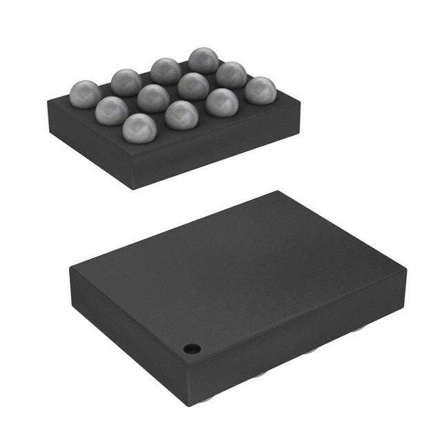
| 产品图片 |
|
| rohs | 符合RoHS无铅 / 符合限制有害物质指令(RoHS)规范要求 |
| 产品系列 | 开关 IC,USB开关IC,Texas Instruments TPS2051BDGNR- |
| 数据手册 | |
| 产品型号 | TPS2051BDGNR |
| Rds(On) | 70 毫欧 |
| 产品目录页面 | |
| 产品种类 | USB开关IC |
| 供应商器件封装 | 8-MSOP-PowerPad |
| 其它名称 | 296-17313-6 |
| 内部开关 | 是 |
| 包装 | Digi-Reel® |
| 商标 | Texas Instruments |
| 安装类型 | 表面贴装 |
| 安装风格 | SMD/SMT |
| 导通电阻—最大值 | 135 mOhms |
| 封装 | Reel |
| 封装/外壳 | 8-TSSOP,8-MSOP(0.118",3.00mm 宽)裸焊盘 |
| 封装/箱体 | HVSSOP-8 |
| 工作温度 | -40°C ~ 85°C |
| 工作温度范围 | - 40 C to + 85 C |
| 工厂包装数量 | 2500 |
| 开关数量 | Single |
| 开关类型 | 通用 |
| 接口 | 开/关 |
| 最大功率耗散 | 1712.3 mW |
| 最大工作温度 | + 85 C |
| 最小工作温度 | - 40 C |
| 标准包装 | 1 |
| 比率-输入:输出 | 1:1 |
| 特性 | - |
| 电压-电源(Vcc/Vdd) | 不需要 |
| 电压-负载 | 2.7 V ~ 5.5 V |
| 电压-输入 | 2.7 V ~ 5.5 V |
| 电流-输出(最大值) | 500mA |
| 电流限制 | 1A |
| 电源电压-最大 | 5.5 V |
| 电源电压-最小 | 2.7 V |
| 电源电流 | 43 uA |
| 空闲时间—最大值 | 10 ms |
| 类型 | 高端开关 |
| 系列 | TPS2051B |
| 输入类型 | 非反相 |
| 输出数 | 1 |
| 输出类型 | N 通道 |
| 输出配置 | 高端 |
| 运行时间—最大值 | 3 ms |
| 配用 | /product-detail/zh/TPS2051BEVM/296-31119-ND/1907567/product-detail/zh/TPS2051BEVM-290/TPS2051BEVM-290-ND/1907568/product-detail/zh/TPS2051BEVM-292/TPS2051BEVM-292-ND/1907569 |


- 商务部:美国ITC正式对集成电路等产品启动337调查
- 曝三星4nm工艺存在良率问题 高通将骁龙8 Gen1或转产台积电
- 太阳诱电将投资9.5亿元在常州建新厂生产MLCC 预计2023年完工
- 英特尔发布欧洲新工厂建设计划 深化IDM 2.0 战略
- 台积电先进制程称霸业界 有大客户加持明年业绩稳了
- 达到5530亿美元!SIA预计今年全球半导体销售额将创下新高
- 英特尔拟将自动驾驶子公司Mobileye上市 估值或超500亿美元
- 三星加码芯片和SET,合并消费电子和移动部门,撤换高东真等 CEO
- 三星电子宣布重大人事变动 还合并消费电子和移动部门
- 海关总署:前11个月进口集成电路产品价值2.52万亿元 增长14.8%


PDF Datasheet 数据手册内容提取
Product Order Technical Tools & Support & Folder Now Documents Software Community TPS2041B,TPS2042B,TPS2043B,TPS2044B TPS2051B,TPS2052B,TPS2053B,TPS2054B SLVS514M–JUNE2010–REVISEDJUNE2016 TPS20xxB Current-Limited, Power-Distribution Switches 1 Features 3 Description • 70-mΩ High-SideMOSFET The TPS20xxB power-distribution switches are 1 intended for applications where heavy capacitive • 500-mAContinuousCurrent loads and short circuits are likely to be encountered. • ThermalandShort-CircuitProtection These devices incorporates 70-mΩ N-channel • AccurateCurrentLimit MOSFET power switches for power-distribution (0.75AMinimum,1.25AMaximum) systems that require multiple power switches in a single package. Each switch is controlled by a logic • OperatingRange:2.7Vto5.5V enable input. Gate drive is provided by an internal • 0.6-msTypicalRiseTime charge pump designed to control the power-switch • UndervoltageLockout rise times and fall times to minimize current surges during switching. The charge pump requires no • DeglitchedFaultReport(OC) external components and allows operation from • NoOC GlitchDuringPowerUp suppliesaslowas2.7V. • MaximumStandbySupplyCurrent: When the output load exceeds the current-limit 1-μA(Single,Dual)or2-μA(Triple,Quad) threshold or a short is present, the device limits the • AmbientTemperatureRange:–40°Cto85°C output current to a safe level by switching into a • ULRecognized,FileNumberE169910 constant-current mode, pulling the overcurrent (OCx) logic output low. When continuous heavy overloads • AdditionalULRecognitionforTPS2042Band and short circuits increase the power dissipation in TPS2052BforGangedConfiguration the switch, causing the junction temperature to rise, a thermal protection circuit shuts off the switch to 2 Applications prevent damage. Recovery from a thermal shutdown • HeavyCapacitiveLoads is automatic once the device has cooled sufficiently. Internal circuitry ensures that the switch remains off • Short-CircuitProtections until valid input voltage is present. This power- distribution switch is designed to set current limit at 1 A(typical). DeviceInformation(1) PARTNUMBER PACKAGE BODYSIZE(NOM) SOIC(8) 4.90mm×3.91mm SOIC(16) 9.90mm×3.91mm TPS20xxB SOT-23(5) 2.90mm×1.60mm HVSSOP(8) 3.00mm×3.00mm SON(8) 3.00mm×3.00mm (1) For all available packages, see the orderable addendum at theendofthedatasheet. TypicalApplicationSchematic TPS2042B Power Supply 2 IN 2.7 V to 5.5 V OUT1 7 Load 0.1µF 0.1µF 22µF 8 OC1 3 6 EN1 OUT2 Load 5 OC2 0.1µF 22µF 4 EN2 GND 1 Copyright © 2016,Texas Instruments Incorporated 1 An IMPORTANT NOTICE at the end of this data sheet addresses availability, warranty, changes, use in safety-critical applications, intellectualpropertymattersandotherimportantdisclaimers.PRODUCTIONDATA.
TPS2041B,TPS2042B,TPS2043B,TPS2044B TPS2051B,TPS2052B,TPS2053B,TPS2054B SLVS514M–JUNE2010–REVISEDJUNE2016 www.ti.com Table of Contents 1 Features.................................................................. 1 9.4 DeviceFunctionalModes........................................20 2 Applications........................................................... 1 10 ApplicationandImplementation........................ 21 3 Description............................................................. 1 10.1 ApplicationInformation..........................................21 4 RevisionHistory..................................................... 2 10.2 TypicalApplication................................................21 5 GeneralSwitchCatalog......................................... 4 11 PowerSupplyRecommendations..................... 35 11.1 UndervoltageLockout(UVLO)..............................35 6 PinConfigurationandFunctions......................... 4 12 Layout................................................................... 35 7 Specifications......................................................... 7 12.1 LayoutGuidelines.................................................35 7.1 AbsoluteMaximumRatings......................................7 12.2 LayoutExample....................................................35 7.2 ESDRatings ............................................................7 12.3 PowerDissipation.................................................35 7.3 RecommendedOperatingConditions.......................7 12.4 ThermalProtection................................................36 7.4 ThermalInformation..................................................7 13 DeviceandDocumentationSupport................. 37 7.5 ElectricalCharacteristics...........................................8 7.6 DissipationRatings...................................................9 13.1 ReceivingNotificationofDocumentationUpdates37 7.7 TypicalCharacteristics............................................10 13.2 RelatedLinks........................................................37 13.3 CommunityResources..........................................37 8 ParameterMeasurementInformation................14 13.4 Trademarks...........................................................37 9 DetailedDescription............................................ 15 13.5 ElectrostaticDischargeCaution............................37 9.1 Overview.................................................................15 13.6 Glossary................................................................37 9.2 FunctionalBlockDiagrams.....................................15 14 Mechanical,Packaging,andOrderable 9.3 FeatureDescription.................................................19 Information........................................................... 37 4 Revision History NOTE:Pagenumbersforpreviousrevisionsmaydifferfrompagenumbersinthecurrentversion. ChangesfromRevisionL(June2011)toRevisionM Page • AddedESDRatingstable,FeatureDescriptionsection,DeviceFunctionalModes,ApplicationandImplementation section,PowerSupplyRecommendationssection,Layoutsection,DeviceandDocumentationSupportsection,and Mechanical,Packaging,andOrderableInformationsection ................................................................................................. 7 ChangesfromRevisionK(June2010)toRevisionL Page • AddednotetoGeneralSwitchCataloglinkatwww.ti.com.................................................................................................... 4 • AddedI spectotheELECCHARATABLE........................................................................................................................ 8 OC • DeletedNottestedinproduction,specifiedbydesign.note2inELECTRICALCHARATABLE.......................................... 8 ChangesfromRevisionJ(December2008)toRevisionK Page • DeletedElectricalCharTablenote-Estimatedvalue.Finalvaluependingcharacterization................................................ 9 ChangesfromRevisionI(October2008)toRevisionJ Page • DeletedProductPreviewfromtheDRBpackage.................................................................................................................. 1 • DeletedElectricalCharTablenote-ThisconfigurationhasnotbeentestedforULcertification.......................................... 9 ChangesfromRevisionH(September2007)toRevisionI Page • AddedFeaturedBullet:AdditionalULRecognition................................................................................................................ 1 • AddedDRB-8pinoutpackage................................................................................................................................................ 1 • AddedDRB-8totheDissipationRatingTable....................................................................................................................... 9 2 SubmitDocumentationFeedback Copyright©2010–2016,TexasInstrumentsIncorporated ProductFolderLinks:TPS2041B TPS2042B TPS2043B TPS2044BTPS2051B TPS2052B TPS2053B TPS2054B
TPS2041B,TPS2042B,TPS2043B,TPS2044B TPS2051B,TPS2052B,TPS2053B,TPS2054B www.ti.com SLVS514M–JUNE2010–REVISEDJUNE2016 ChangesfromRevisionG(OCTOBER2006)toRevisionH Page • UpdatedtheGeneralSwitchCatalogtable............................................................................................................................ 4 ChangesfromRevisionF(June2006)toRevisionG Page • DeletedProductPreviewfromtheDBVpackage................................................................................................................... 1 • AddedTPS20601.5AandTPS20641.5AtotheGeneralSwitchCatalogtable................................................................. 4 • AddedtheDBVPACKAGEtotheTerminalFunctionstable.................................................................................................. 5 • AddedD,DGNandDBVpackageoptionstother TestCondition ............................................................................... 8 DS(on) Copyright©2010–2016,TexasInstrumentsIncorporated SubmitDocumentationFeedback 3 ProductFolderLinks:TPS2041B TPS2042B TPS2043B TPS2044BTPS2051B TPS2052B TPS2053B TPS2054B
TPS2041B,TPS2042B,TPS2043B,TPS2044B TPS2051B,TPS2052B,TPS2053B,TPS2054B SLVS514M–JUNE2010–REVISEDJUNE2016 www.ti.com 5 General Switch Catalog GENERALSWITCH CATALOG 33 mW, Single 80 mW, Single 80 mW, Dual 80 mW, Dual 80 mW,Triple 80 mW, Quad 80 mW, Quad TPS201xA 0.2Ato 2A TPS2014 600 mA TPS202x 0.2Ato 2A TPS2015 1A TPS203x 0.2Ato 2A TPS2041B 500 mA TPS2042B 500 mA TPS2080 500 mA TPS2051B 500 mA TPS2052B 500 mA TPS2081 500 mA TPS2045A 250 mA TPS2046B 250 mA TPS2082 500 mA TPS2043B 500 mA TTTTPPPPSSSS2222000045669515 A 111205AA00 mmAA TTTTPPPPSSSS2222000056666260 21115.AA50A mA TTTPPPSSS222000999012 222555000 mmmAAA TTTTPPPPSSSS2222000054563773BBA 1252505A000 mmmAAA TTTPPPSSS222000454448BBA 255500000 mmmAAA TTTPPPSSS222000888567 555000000 mmmAAA TPS2068 1.5A TPS2064 1.5A TPS2067 1A TPS2058 250 mA TPS2095 250 mA TPS2069 1.5A TPS2096 250 mA TPS2097 250 mA SeeTISwitchPortfolioathttp://www.ti.com/usbpower 6 Pin Configuration and Functions TPS2041BandTPS2051B:DBVPackage 5-PinSOT-23 TPS2042BandTPS2052B:DRBPackage TopView 8-PinSON TopView OUT IN GND 1 8 OC1 GND IN 2 7 OUT1 OC EN† EN1† 3 6 OUT2 EN2† 4 5 OC2 †Allenableoutputsareactivehighforthe TPS205xBseries. †Allenableoutputsareactivehighforthe TPS205xBseries. TPS2041BandTPS2051B:DandDGNPackages 8-PinSOICandHVSSOP TPS2043BandTPS2053B:DPackage TopView 16-PinSOIC TopView GND 1 8 OUT IN 2 7 OUT GND 1 16 OC1 IN 3 6 OUT IN1 2 15 OUT1 EN† 4 5 OC EN1† 3 14 OUT2 EN2† 4 13 OC2 †Allenableoutputsareactivehighforthe GND 5 12 OC3 TPS205xBseries. IN2 6 11 OUT3 EN3† 7 10 NC NC 8 9 NC TPS2042BandTPS2052B:DandDGNPackages 8-PinSOICandHVSSOP †Allenableoutputsareactivehighforthe TopView TPS205xBseries. GND 1 8 OC1 IN 2 7 OUT1 TPS2044BandTPS2054B:DPackage EN1† 3 6 OUT2 16-PinSOIC EN2† 4 5 OC2 TopView †Allenableoutputsareactivehighforthe TPS205xBseries. GND 1 16 OC1 IN1 2 15 OUT1 EN1† 3 14 OUT2 EN2† 4 13 OC2 GND 5 12 OC3 IN2 6 11 OUT3 EN3† 7 10 OUT4 EN4† 8 9 OC4 †Allenableoutputsareactivehighforthe TPS205xBseries. 4 SubmitDocumentationFeedback Copyright©2010–2016,TexasInstrumentsIncorporated ProductFolderLinks:TPS2041B TPS2042B TPS2043B TPS2044BTPS2051B TPS2052B TPS2053B TPS2054B
TPS2041B,TPS2042B,TPS2043B,TPS2044B TPS2051B,TPS2052B,TPS2053B,TPS2054B www.ti.com SLVS514M–JUNE2010–REVISEDJUNE2016 PinFunctions(TPS2041BandTPS2051B) PIN TPS2041B TPS2051B TPS2041B TPS2051B I/O DESCRIPTION NAME SOICANDDGN SOT-23 EN 4 — 4 — I Enableinput,logiclowturnsonpowerswitch EN — 4 — 4 I Enableinput,logichighturnsonpowerswitch GND 1 1 2 2 — Ground IN 2,3 2,3 5 5 I Inputvoltage OC 5 5 3 3 O Overcurrentopen-drainoutput,active-low OUT 6,7,8 6,7,8 1 1 O Power-switchoutput PinFunctions(TPS2042BandTPS2052B) PIN TPS2042B TPS2052B I/O DESCRIPTION NAME SOIC,HVSSOP,SON EN1 3 — I Enableinput,logiclowturnsonpowerswitchIN-OUT1 EN2 4 — I Enableinput,logiclowturnsonpowerswitchIN-OUT2 EN1 — 3 I Enableinput,logichighturnsonpowerswitchIN-OUT1 EN2 — 4 I Enableinput,logichighturnsonpowerswitchIN-OUT2 GND 1 1 — Ground IN 2 2 I Inputvoltage OC1 8 8 O Overcurrent,open-drainoutput,activelow,IN-OUT1 OC2 5 5 O Overcurrent,open-drainoutput,activelow,IN-OUT2 OUT1 7 7 O Power-switchoutput,IN-OUT1 OUT2 6 6 O Power-switchoutput,IN-OUT2 PowerPAD InternallyconnectedtoGND;usedtoheat-sinktheparttothecircuitboard — — — ™ traces.ShouldbeconnectedtoGNDpin. PinFunctions(TPS2043BandTPS2053B) PIN TPS2043B TPS2053B I/O DESCRIPTION NAME SOIC SOIC EN1 3 — I Enableinput,logiclowturnsonpowerswitchIN1-OUT1 EN2 4 — I Enableinput,logiclowturnsonpowerswitchIN1-OUT2 EN3 7 — I Enableinput,logiclowturnsonpowerswitchIN2-OUT3 EN1 — 3 I Enableinput,logichighturnsonpowerswitchIN1-OUT1 EN2 — 4 I Enableinput,logichighturnsonpowerswitchIN1-OUT2 EN3 — 7 I Enableinput,logichighturnsonpowerswitchIN2-OUT3 GND 1,5 1,5 — Ground IN1 2 2 I InputvoltageforOUT1andOUT2 IN2 6 6 I InputvoltageforOUT3 NC 8,9,10 8,9,10 — Noconnection OC1 16 16 O Overcurrent,open-drainoutput,activelow,IN1-OUT1 OC2 13 13 O Overcurrent,open-drainoutput,activelow,IN1-OUT2 OC3 12 12 O Overcurrent,open-drainoutput,activelow,IN2-OUT3 OUT1 15 15 O Power-switchoutput,IN1-OUT1 OUT2 14 14 O Power-switchoutput,IN1-OUT2 OUT3 11 11 O Power-switchoutput,IN2-OUT3 Copyright©2010–2016,TexasInstrumentsIncorporated SubmitDocumentationFeedback 5 ProductFolderLinks:TPS2041B TPS2042B TPS2043B TPS2044BTPS2051B TPS2052B TPS2053B TPS2054B
TPS2041B,TPS2042B,TPS2043B,TPS2044B TPS2051B,TPS2052B,TPS2053B,TPS2054B SLVS514M–JUNE2010–REVISEDJUNE2016 www.ti.com PinFunctions(TPS2044BandTPS2054B) PIN TPS2044B TPS2054B I/O DESCRIPTION NAME SOIC SOIC EN1 3 — I Enableinput,logiclowturnsonpowerswitchIN1-OUT1 EN2 4 — I Enableinput,logiclowturnsonpowerswitchIN1-OUT2 EN3 7 — I Enableinput,logiclowturnsonpowerswitchIN2-OUT3 EN4 8 — I Enableinput,logiclowturnsonpowerswitchIN2-OUT4 EN1 — 3 I Enableinput,logichighturnsonpowerswitchIN1-OUT1 EN2 — 4 I Enableinput,logichighturnsonpowerswitchIN1-OUT2 EN3 — 7 I Enableinput,logichighturnsonpowerswitchIN2-OUT3 EN4 — 8 I Enableinput,logichighturnsonpowerswitchIN2-OUT4 GND 1,5 1,5 — Ground IN1 2 2 I InputvoltageforOUT1andOUT2 IN2 6 6 I InputvoltageforOUT3andOUT4 OC1 16 16 O Overcurrent,open-drainoutput,activelow,IN1-OUT1 OC2 13 13 O Overcurrent,open-drainoutput,activelow,IN1-OUT2 OC3 12 12 O Overcurrent,open-drainoutput,activelow,IN2-OUT3 OC4 9 9 O Overcurrent,open-drainoutput,activelow,IN2-OUT4 OUT1 15 15 O Power-switchoutput,IN1-OUT1 OUT2 14 14 O Power-switchoutput,IN1-OUT2 OUT3 11 11 O Power-switchoutput,IN2-OUT3 OUT4 10 10 O Power-switchoutput,IN2-OUT4 6 SubmitDocumentationFeedback Copyright©2010–2016,TexasInstrumentsIncorporated ProductFolderLinks:TPS2041B TPS2042B TPS2043B TPS2044BTPS2051B TPS2052B TPS2053B TPS2054B
TPS2041B,TPS2042B,TPS2043B,TPS2044B TPS2051B,TPS2052B,TPS2053B,TPS2054B www.ti.com SLVS514M–JUNE2010–REVISEDJUNE2016 7 Specifications 7.1 Absolute Maximum Ratings overoperatingfree-airtemperaturerange(unlessotherwisenoted) (1) MIN MAX UNIT V ,V Inputvoltage (2) –0.3 6 V I(IN) I(INx) V ,V (2) Outputvoltage –0.3 6 V O(OUT) O(OUTx) V ,V ,V , I(EN) I(ENx) I(EN) Inputvoltage –0.3 6 V V I(ENx) V ,V Voltagerange –0.3 6 V I(/OC) I(OCx) I ,I Continuousoutputcurrent Internallylimited O(OUT) O(OUTx) Continuoustotalpowerdissipation SeeDissipationRatings T Operatingvirtualjunctiontemperature –40 125 °C J T Storagetemperature –65 150 °C stg (1) StressesbeyondthoselistedunderAbsoluteMaximumRatingsmaycausepermanentdamagetothedevice.Thesearestressratings only,whichdonotimplyfunctionaloperationofthedeviceattheseoranyotherconditionsbeyondthoseindicatedunderRecommended OperatingConditions.Exposuretoabsolute-maximum-ratedconditionsforextendedperiodsmayaffectdevicereliability. (2) AllvoltagesarewithrespecttoGND. 7.2 ESD Ratings VALUE UNIT Humanbodymodel(HBM),perANSI/ESDA/JEDECJS-001,allpins(1) ±2000 V(ESD) Electrostaticdischarge Chargeddevicemodel(CDM),perJEDECspecificationJESD22-C101, V allpins(2) ±500 (1) JEDECdocumentJEP155statesthat500-VHBMallowssafemanufacturingwithastandardESDcontrolprocess. (2) JEDECdocumentJEP157statesthat250-VCDMallowssafemanufacturingwithastandardESDcontrolprocess. 7.3 Recommended Operating Conditions overoperatingfree-airtemperaturerange(unlessotherwisenoted) MIN NOM MAX UNIT V ,V Inputvoltage 2.7 5.5 V I(IN) I(INx) V ,V ,V , I(EN) I(ENx) I(EN) Inputvoltage 0 5.5 V V I(ENx) I ,I Continuousoutputcurrent 0 500 mA O(OUT) O(OUTx) T Operatingvirtualjunctiontemperature –40 125 °C J 7.4 Thermal Information TPS2042xxandTPS2053xx THERMALMETRIC(1) D DBV DGN DRB UNIT (SOIC) (SOT-23) (HVSSOP) (SON) 8PINS 16PINS 5PINS 8PINS 8PINS R Junction-to-ambientthermalresistance 119.3 81.6 208.6 53.6 47.5 °C/W θJA R Junction-to-case(top)thermalresistance 67.6 42.7 122.9 58.7 53 °C/W θJC(top) R Junction-to-boardthermalresistance 59.6 39.1 37.8 35.5 14.2 °C/W θJB ψ Junction-to-topcharacterizationparameter 20.3 10.4 14.6 2.7 1.2 °C/W JT Junction-to-boardcharacterization ψ 59.1 38.8 36.9 35.3 14.2 °C/W JB parameter Junction-to-case(bottom)thermal R N/A N/A N/A 6.7 7.3 °C/W θJC(bot) resistance (1) Formoreinformationabouttraditionalandnewthermalmetrics,seetheSemiconductorandICPackageThermalMetricsapplication report. Copyright©2010–2016,TexasInstrumentsIncorporated SubmitDocumentationFeedback 7 ProductFolderLinks:TPS2041B TPS2042B TPS2043B TPS2044BTPS2051B TPS2052B TPS2053B TPS2054B
TPS2041B,TPS2042B,TPS2043B,TPS2044B TPS2051B,TPS2052B,TPS2053B,TPS2054B SLVS514M–JUNE2010–REVISEDJUNE2016 www.ti.com 7.5 Electrical Characteristics overrecommendedoperatingjunctiontemperaturerange,V =5.5V,I =0.5A,V =0V(unlessotherwisenoted) I(IN) O I(/ENx) PARAMETER TESTCONDITIONS(1) MIN TYP MAX UNIT POWERSWITCH Staticdrain-sourceon-state DandDGNpackages 70 135 V =5Vor3.3V,I =0.5A, resistance,5-Voperation I(IN) O mΩ and3.3-Voperation -40°C≤TJ≤125°C DBVpackageonly 95 140 r Staticdrain-sourceon-state V =2.7V,I =0.5A, DS(on) I(IN) O DandDGNpackages 75 150 mΩ resistance,2.7-Voperation –40°C≤T ≤125°C J Staticdrain-sourceon-state V =5V,I =1A,OUT1andOUT2 DGNpackage, I(IN) O 49 mΩ resistance,5-Voperation connected,0°C≤T ≤70°C TPS2042B/52B J V =5.5V 0.6 1.5 I(IN) t Risetime,output r VI(IN)=2.7V CL=1μF, T =25°C 0.4 1 ms VI(IN)=5.5V RL=10Ω J 0.05 0.5 t Falltime,output f V =2.7V 0.05 0.5 I(IN) ENABLEINPUTENANDENx V High-levelinputvoltage 2.7V≤V ≤5.5V 2 IH I(IN) V V Low-levelinputvoltage 2.7V≤V ≤5.5V 0.8 IL I(IN) I Inputcurrent V =0Vor5.5V –0.5 0.5 μA I I(ENx) t Turnontime C =100μF,R =10Ω 3 on L L ms t Turnofftime C =100μF,R =10Ω 10 off L L CURRENTLIMIT VI(IN)=5V,OUTconnectedtoGND, TJ=25°C 0.75 1 1.25 deviceenabledintoshort-circuit –40°C≤T ≤125°C 0.7 1 1.3 J I Short-circuitoutputcurrent A OS V =5V,OUT1andOUT2connectedto I(IN) 0°C≤T ≤70°C GND,deviceenabledintoshort-circuit, J 1.5 TPS2042B/52B measureatIN TPS2041B/51B I 1.5 1.9 OS I Overcurrenttripthreshold V =5V,100A/s A OC IN TPS2042B/52B I 1.55 2 OS SUPPLYCURRENT(TPS2041B,TPS2051B) Supplycurrent,low-leveloutput NoloadonOUT,VI(ENx)=5.5V, TJ=25°C 0.5 1 μA orVI(ENx)=0V -40°°C≤TJ≤125°C 0.5 5 Supplycurrent,high-leveloutput NoloadonOUT,VI(ENx)=0V, TJ=25°C 43 60 μA orVI(ENx)=5.5V –40°C≤TJ≤125°C 43 70 OUTconnectedtoground,V =5.5V, Leakagecurrent I(ENx) –40°C≤T ≤125°C 1 μA orV =0V J I(ENx) Reverseleakagecurrent V =5.5V,IN=ground T =25°C 0 μA I(OUTx) J (1) Pulse-testingtechniquesmaintainjunctiontemperatureclosetoambienttemperature;thermaleffectsmustbetakenintoaccount separately. 8 SubmitDocumentationFeedback Copyright©2010–2016,TexasInstrumentsIncorporated ProductFolderLinks:TPS2041B TPS2042B TPS2043B TPS2044BTPS2051B TPS2052B TPS2053B TPS2054B
TPS2041B,TPS2042B,TPS2043B,TPS2044B TPS2051B,TPS2052B,TPS2053B,TPS2054B www.ti.com SLVS514M–JUNE2010–REVISEDJUNE2016 Electrical Characteristics (continued) overrecommendedoperatingjunctiontemperaturerange,V =5.5V,I =0.5A,V =0V(unlessotherwisenoted) I(IN) O I(/ENx) PARAMETER TESTCONDITIONS(1) MIN TYP MAX UNIT SUPPLYCURRENT(TPS2042B,TPS2052B) T =25°C 0.5 1 J Supplycurrent,low-leveloutput NoloadonOUT,V =5.5V μA I(ENx) –40°C≤T ≤125°C 0.5 5 J T =25°C 50 70 J Supplycurrent,high-leveloutput NoloadonOUT,V =0V μA I(ENx) –40°C≤T ≤125°C 50 90 J Leakagecurrent OUTconnectedtoground,V =5.5V –40°C≤T ≤125°C 1 μA I(ENx) J Reverseleakagecurrent V =5.5V,IN=ground T =25°C 0.2 μA I(OUTx) J SUPPLYCURRENT(TPS2043B,TPS2053B) T =25°C 0.5 2 J Supplycurrent,low-leveloutput NoloadonOUT,V =0V μA I(ENx) –40°C≤T ≤125°C 0.5 10 J T =25°C 65 90 J Supplycurrent,high-leveloutput NoloadonOUT,V =5.5V μA I(ENx) –40°C≤T ≤125°C 65 110 J Leakagecurrent OUTconnectedtoground,V =0V –40°C≤T ≤125°C 1 μA I(ENx) J Reverseleakagecurrent V =5.5V,INx=ground T =25°C 0.2 μA I(OUTx) J SUPPLYCURRENT(TPS2044B,TPS2054B) Supplycurrent,low-leveloutput NoloadonOUT,VI(ENx)=5.5V, TJ=25°C 0.5 2 μA orVI(ENx)=0V –40°C≤TJ≤125°C 0.5 10 Supplycurrent,high-leveloutput NoloadonOUT,VI(ENx)=0V, TJ=25°C 75 110 μA orVI(ENx)=5.5V –40°C≤TJ≤125°C 75 140 OUTconnectedtoground,V =5.5V, Leakagecurrent I(ENx) –40°C≤T ≤125°C 1 μA orV =0V J I(ENx) Reverseleakagecurrent V =5.5V,INx=ground T =25°C 0.2 μA I(OUTx) J UNDERVOLTAGELOCKOUT Low-levelinputvoltage,IN,INx 2 2.5 V Hysteresis,IN,INx T =25°C 75 mV J OVERCURRENTOCandOCx Outputlowvoltage,V I =5mA 0.4 V OL(/OCx) O(OCx) Off-statecurrent V =5Vor3.3V 1 μA O(OCx) OCdeglitch OCxassertionordeassertion 4 8 15 ms THERMALSHUTDOWN(2) Thermalshutdownthreshold 135 °C Recoveryfromthermalshutdown 125 °C Hysteresis 10 °C (2) Thethermalshutdownonlyreactsunderovercurrentconditions. 7.6 Dissipation Ratings THERMAL T ≤25°C DERATINGFACTOR T =70°C T =85°C PACKAGE A A A RESISTANCE,θ POWERRATING ABOVET =25°C POWERRATING POWERRATING JA A DGN-8 1712.3mW 17.123mW/°C 941.78mW 684.93mW D-8 585.82mW 5.8582mW/°C 322.20mW 234.32mW D-16 898.47mW 8.9847mW/°C 494.15mW 359.38mW DBV-5 285mW 2.85mW/°C 155mW 114mW DRB-8(Low-K)(1) 270°CW 370mW 3.71mW/°C 203mW 148mW DRB-8(High-K)(2) 60°CW 1600mW 16.67mW/°C 916mW 866mW (1) SolderedPowerPADonastandard2-layerPCBwithoutviasforthermalpad.SeeTIapplicationnoteSLMA002forfurtherdetails. (2) SolderedPowerPADonastandard4-layerPCBwithviasforthermalpad.SeeTIapplicationnoteSLMA002forfurtherdetails. Copyright©2010–2016,TexasInstrumentsIncorporated SubmitDocumentationFeedback 9 ProductFolderLinks:TPS2041B TPS2042B TPS2043B TPS2044BTPS2051B TPS2052B TPS2053B TPS2054B
TPS2041B,TPS2042B,TPS2043B,TPS2044B TPS2051B,TPS2052B,TPS2053B,TPS2054B SLVS514M–JUNE2010–REVISEDJUNE2016 www.ti.com 7.7 Typical Characteristics 1.0 3.3 CL= 100µF, CL= 100µF, 0.9 RL= 10Ω, RL= 10Ω, TA= 25°C TA= 25°C 0.8 3.2 ms 0.7 ms Tiurnon Tme− 000...456 Turnoff ime−T 3.13 0.3 0.2 2.9 0.1 0 2.8 2 3 4 5 6 2 3 4 5 6 VI−Input Voltage−V VI−Input Voltage−V Figure1.TurnonTimevsInputVoltage Figure2.TurnoffTimevsInputVoltage 0.6 0.25 CL= 1µF, CL= 1µF, RL= 10Ω, RL= 10Ω, 0.5 TA= 25°C TA= 25°C 0.2 0.4 ms ms 0.15 − − Riise Tme 0.3 Fiall Tme 0.1 0.2 0.05 0.1 0 0 2 3 4 5 6 2 3 4 5 6 VI−Input Voltage−V VI−Input Voltage−V \ Figure3.RiseTimevsInputVoltage Figure4.FallTimevsInputVoltage 60 70 A A d−µ 50 VI= 5.5 V µd− 60 VI= 5.5 V able VI= 5 V able En En 50 Output 40 Output 40 VI= 3.3 V VI= 5 V Supply Current, 2300 VI= 3.3 V VI= 2.7 V Supply Current, 2300 VI= 2.7 V −II (IN) 100 −II (IN) 100 −50 0 50 100 150 −50 0 50 100 150 TJ−Junction Temperature−°C TJ−Junction Temperature−°C Figure5.TPS2041BandTPS2051BSupplyCurrent,Output Figure6.TPS2042BandTPS2052BSupplyCurrent,Output EnabledvsJunctionTemperature EnabledvsJunctionTemperature 10 SubmitDocumentationFeedback Copyright©2010–2016,TexasInstrumentsIncorporated ProductFolderLinks:TPS2041B TPS2042B TPS2043B TPS2044BTPS2051B TPS2052B TPS2053B TPS2054B
TPS2041B,TPS2042B,TPS2043B,TPS2044B TPS2051B,TPS2052B,TPS2053B,TPS2054B www.ti.com SLVS514M–JUNE2010–REVISEDJUNE2016 Typical Characteristics (continued) 90 120 µAed− 80 VI= 5.5 V µAed− 100 VI= 5.5 V abl 70 abl VI= 5 V n n E E ut 60 VI= 5 V ut 80 utp VI= 3.3 V utp nt, O 50 nt, O 60 e e Curr 40 VI= 2.7 V Curr VI= 2.7 V pply 30 pply 40 VI= 3.3 V u u −S 20 −S II (IN) 10 II (IN) 20 0 0 −50 0 50 100 150 −50 0 50 100 150 TJ−Junction Temperature−°C TJ−Junction Temperature−°C Figure7.TPS2043BandTPS2053BSupplyCurrent,Output Figure8.TPS2044BTPS2054BSupplyCurrent,Output EnabledvsJunctionTemperature EnabledvsJunctionTemperature 0.5 0.5 µA−Supply Current, Output Disabled− 00000000....1234....12345555 VVII== 2 5.7 V VVI= 5V.5I =V 3.3 V µ−Supply ACurrent, Output Disabled− 00000000....1234....12345555 VIV=I 2=. 75 .V5 V VVII== 5 3 V.3 V N) N) II (I 0.05 II (I 0.05 0 0 −50 0 50 100 150 −50 0 50 100 150 TJ−Junction Temperature−°C TJ−Junction Temperature−°C Figure9.TPS2041BTPS2051BSupplyCurrent,Output Figure10.TPS2042BandTPS2052BSupplyCurrent,Output DisabledvsJunctionTemperature DisabledvsJunctionTemperature 0.5 0.5 µ−SupplyA Current, Output Disabled− 00000000....1234....12345555 VI=V 3I.=3 5V V VI= 5V.5I =V 2.7 V µA−Supply Current, Output Disabled− 00000000....1234....12345555 VI= 2.7 VVI= 5.5 VVIV=I 3=. 35 VV N) N) II (I 0.05 II (I 0.05 0 0 −50 0 50 100 150 −50 0 50 100 150 TJ−Junction Temperature−°C TJ−Junction Temperature−°C Figure11.TPS2043BandTPS2053BSupplyCurrent,Output Figure12.TPS2044BandTPS2054BSupplyCurrent,Output DisabledvsJunctionTemperature DisabledvsJunctionTemperature Copyright©2010–2016,TexasInstrumentsIncorporated SubmitDocumentationFeedback 11 ProductFolderLinks:TPS2041B TPS2042B TPS2043B TPS2044BTPS2051B TPS2052B TPS2053B TPS2054B
TPS2041B,TPS2042B,TPS2043B,TPS2044B TPS2051B,TPS2052B,TPS2053B,TPS2054B SLVS514M–JUNE2010–REVISEDJUNE2016 www.ti.com Typical Characteristics (continued) Ω 120 1.08 m IO= 0.5A Static Drain-Source On-State Resistance− 12468000000 VI = 5 V VI= 2.7V VI = 3.3 V −ShAort-Circuit Output Current−IOS 00001111.......9999000.02468246 VI= 3.3 VVVII== 25..7V5 I VV= 5 V − n) 0 0.9 S(o −50 0 50 100 150 −50 0 50 100 150 rD TJ−Junction Temperature−°C TJ−Junction Temperature−°C Figure13.StaticDrain-Sourceon-StateResistancevs Figure14.Short-CircuitOutputCurrentvsJunction JunctionTemperature Temperature 2 2 TA= 25°C TTPPSS22004412BB,, TLAoa=d 2 R5a°Cmp = 1A/10 ms Load Ramp = 1A/10 ms TPS2051B, 1.8 TPS2052B 1.8 A A − − rThreshold ip CurrentT 11..46 Threshrip Currold Tent 11..46 1.2 1.2 TPS2043B, TPS2044B, TPS2053B, TPS2054B 1 1 2.5 3 3.5 4 4.5 5 5.5 6 2.5 3 3.5 4 4.5 5 5.5 6 VI−Input Voltage−V VI−Input Voltage−V Figure15.ThresholdTripCurrentvsInputVoltage Figure16.ThresholdTripCurrentvsInputVoltage 2.3 100 VI= 5 V, TA= 25°C −V 2.26 UVLO Rising s 80 out −µ dervoltage Lock 22..1282 UVLO Falling Limit Response 4600 Un nt- O− urre L C UV 2.14 20 2.1 0 −50 0 50 100 150 0 2.5 5 7.5 10 12.5 TJ−Junction Temperature−°C Peak Current−A Figure17.UndervoltageLockoutvsJunctionTemperature Figure18.Current-LimitResponsevsPeakCurrent 12 SubmitDocumentationFeedback Copyright©2010–2016,TexasInstrumentsIncorporated ProductFolderLinks:TPS2041B TPS2042B TPS2043B TPS2044BTPS2051B TPS2052B TPS2053B TPS2054B
TPS2041B,TPS2042B,TPS2043B,TPS2044B TPS2051B,TPS2052B,TPS2053B,TPS2054B www.ti.com SLVS514M–JUNE2010–REVISEDJUNE2016 Typical Characteristics (continued) VV5 IIV((EE/NNd))iv RCTALL=== 21150µ°FΩC, VV5 IIV((EE/NNd))iv V2 OV(/OdUivT) RCLL== 110µFΩ, VO(OUT) TA= 25°C 2 V/div t−Time−500µs/div t−Time−500µs/div Figure19.TurnonDelayandRiseTimeWith1-µFLoad Figure20.TurnoffDelayandFallTimeWith1-µFLoad VVII((EENN)) RCTALL=== 211500°0ΩCµ,F VV5 IIV((EE/NNd))iv 5 V/div RL= 10Ω, VO(OUT) CL= 100µF VO(OUT) 2 V/div TA= 25°C 2 V/div t−Time−500µs/div t−Time−500µs/div Figure21.TurnonDelayandRiseTimeWith100-µFLoad Figure22.TurnoffDelayandFallTimeWith100-µFLoad VV5 IIV((EE/NNd))iv VV5 IIV((EE/NNd))iv VRTAIL=== 5 21 5V0,°ΩC, 220µF 470µF IO(OUT) IO(OUT) 500 mA/div 500 mA/div 100µF t−Time−500µs/div t−Time−500µs/div Figure23.Short-CircuitCurrent, Figure24.InrushCurrentWithDifferent DeviceEnabledIntoShort LoadCapacitance Copyright©2010–2016,TexasInstrumentsIncorporated SubmitDocumentationFeedback 13 ProductFolderLinks:TPS2041B TPS2042B TPS2043B TPS2044BTPS2051B TPS2052B TPS2053B TPS2054B
TPS2041B,TPS2042B,TPS2043B,TPS2044B TPS2051B,TPS2052B,TPS2053B,TPS2054B SLVS514M–JUNE2010–REVISEDJUNE2016 www.ti.com Typical Characteristics (continued) VO(OC) VO(OC) 2 V/div 2 V/div 500 mIOA(O/dUiTv) 500 mIOA(O/dUiTv) t−Time−2 ms/div t−Time−2 ms/div Figure25.3-ΩLoadConnectedtoEnabledDevice Figure26.2-ΩLoadConnectedtoEnabledDevice 8 Parameter Measurement Information OUT tr tf RL CL VO(OUT) 90% 90% 10% 10% TEST CIRCUIT VI(EN) 50% 50% VI(EN) 50% 50% ton toff ton toff VO(OUT) 90% VO(OUT) 90% 10% 10% VOLTAGE WAVEFORMS Figure27. TestCircuitandVoltageWaveforms 14 SubmitDocumentationFeedback Copyright©2010–2016,TexasInstrumentsIncorporated ProductFolderLinks:TPS2041B TPS2042B TPS2043B TPS2044BTPS2051B TPS2052B TPS2053B TPS2054B
TPS2041B,TPS2042B,TPS2043B,TPS2044B TPS2051B,TPS2052B,TPS2053B,TPS2054B www.ti.com SLVS514M–JUNE2010–REVISEDJUNE2016 9 Detailed Description 9.1 Overview The TPS20xxB are current-limited, power-distribution switches providing 0.5-A continuous load current. These devices incorporates 70-mΩ N-channel MOSFET power switches for power-distribution systems that require multiple power switches in a single package. Gate driver is provided by an internal charge pump designed to minimize current surges during switching. The charge pump requires no external components and allows operationsuppliesaslowas2.7V. 9.2 Functional Block Diagrams (See NoteA) IN CS OUT Charge Pump Current EN Driver Limit (See Note B) OC UVLO Thermal Deglitch GND Sense NoteA: Current sense Note B:Active low (EN) forTPS2041B;Active high (EN) forTPS2051B Figure28. FunctionalBlockDiagram(TPS2041BandTPS2051B) Copyright©2010–2016,TexasInstrumentsIncorporated SubmitDocumentationFeedback 15 ProductFolderLinks:TPS2041B TPS2042B TPS2043B TPS2044BTPS2051B TPS2052B TPS2053B TPS2054B
TPS2041B,TPS2042B,TPS2043B,TPS2044B TPS2051B,TPS2052B,TPS2053B,TPS2054B SLVS514M–JUNE2010–REVISEDJUNE2016 www.ti.com Functional Block Diagrams (continued) OC1 GND Thermal Deglitch Sense EN1 (See Note B) Current Driver Limit Charge Pump (See NoteA) CS OUT1 UVLO (See NoteA) IN CS OUT2 Charge Pump Current Driver Limit OC2 EN2 (See Note B) Thermal Deglitch Sense NoteA: Current sense Note B:Active low (ENx) forTPS2042B;Active high (ENx) forTPS2052B Figure29. FunctionalBlockDiagram(TPS2042BandTPS2052B) 16 SubmitDocumentationFeedback Copyright©2010–2016,TexasInstrumentsIncorporated ProductFolderLinks:TPS2041B TPS2042B TPS2043B TPS2044BTPS2051B TPS2052B TPS2053B TPS2054B
TPS2041B,TPS2042B,TPS2043B,TPS2044B TPS2051B,TPS2052B,TPS2053B,TPS2054B www.ti.com SLVS514M–JUNE2010–REVISEDJUNE2016 Functional Block Diagrams (continued) OC1 Thermal GND Sense Deglitch EN1 (See Note B) Current Driver Limit (See NoteA) CS OUT1 UVLO (See NoteA) IN1 CS OUT2 Current Driver Limit OC2 EN2 (See Note B) Thermal Deglitch Sense Charge VCC Pump Selector (See NoteA) IN2 CS OUT3 Current EN3 Driver Limit (See Note B) OC3 UVLO Thermal Deglitch GND Sense NoteA: Current sense Note B:Active low (ENx) forTPS2043B;Active high (ENx) forTPS2053B Figure30. FunctionalBlockDiagram(TPS2043BandTPS2053B) Copyright©2010–2016,TexasInstrumentsIncorporated SubmitDocumentationFeedback 17 ProductFolderLinks:TPS2041B TPS2042B TPS2043B TPS2044BTPS2051B TPS2052B TPS2053B TPS2054B
TPS2041B,TPS2042B,TPS2043B,TPS2044B TPS2051B,TPS2052B,TPS2053B,TPS2054B SLVS514M–JUNE2010–REVISEDJUNE2016 www.ti.com Functional Block Diagrams (continued) OC1 GND Thermal Deglitch Sense EN1 (See Note B) Current Driver Limit (See NoteA) CS OUT1 UVLO Power Switch (See NoteA) IN1 CS OUT2 Current Driver Limit OC2 EN2 (See Note B) Thermal Deglitch Sense VCC Charge Selector Pump OC3 Thermal Deglitch Sense EN3 (See Note B) Current Driver Limit (See NoteA) CS OUT3 UVLO Power Switch (See NoteA) IN2 CS OUT4 Current Driver Limit OC4 EN4 (See Note B) Thermal Deglitch Sense GND NoteA: Current sense Note B:Active low (ENx) forTPS2044B;Active high (ENx) forTPS2054B Figure31. FunctionalBlockDiagram(TPS2044BandTPS2054B) 18 SubmitDocumentationFeedback Copyright©2010–2016,TexasInstrumentsIncorporated ProductFolderLinks:TPS2041B TPS2042B TPS2043B TPS2044BTPS2051B TPS2052B TPS2053B TPS2054B
TPS2041B,TPS2042B,TPS2043B,TPS2044B TPS2051B,TPS2052B,TPS2053B,TPS2054B www.ti.com SLVS514M–JUNE2010–REVISEDJUNE2016 9.3 Feature Description 9.3.1 PowerSwitch The power switch is an N-channel MOSFET with a low on-state resistance. Configured as a high-side switch, the power switch prevents current flow from OUT to IN and IN to OUT when disabled. The power switch supplies a minimumcurrentof500mA. 9.3.2 ChargePump An internal charge pump supplies power to the driver circuit and provides the necessary voltage to pull the gate of the MOSFET above the source. The charge pump operates from input voltages as low as 2.7 V and requires littlesupplycurrent. 9.3.3 Driver The driver controls the gate voltage of the power switch. To limit large current surges and reduce the associated electromagnetic interference (EMI) produced, the driver incorporates circuitry that controls the rise times and fall timesoftheoutputvoltage. 9.3.4 Enable(ENx) The logic enable pin disables the power switch and the bias for the charge pump, driver, and other circuitry to reduce the supply current. The supply current is reduced to less than 1 µA or 2 µA when a logic high is present on EN. A logic zero input on EN restores bias to the drive and control circuits and turns the switch on. The enableinputiscompatiblewithbothTTLandCMOSlogiclevels. 9.3.5 Enable(ENx) Thelogicenabledisablesthepowerswitchandthebiasforthechargepump,driver,andothercircuitrytoreduce thesupplycurrent.Thesupplycurrentisreducedtolessthan1 μAor2μAwhenalogiclowispresentonENx.A logic high input on ENx restores bias to the drive and control circuits and turns the switch on. The enable input is compatiblewithbothTTLandCMOSlogiclevels. 9.3.6 Overcurrent(OCx) The OCx open-drain output is asserted (active low) when an overcurrent or overtemperature condition is encountered. The output remains asserted until the overcurrent or overtemperature condition is removed. A 10- ms deglitch circuit prevents the OCx signal from oscillation or false triggering. If an overtemperature shutdown occurs,theOCx isassertedinstantaneously. 9.3.7 CurrentSense A sense FET monitors the current supplied to the load. The sense FET measures current more efficiently than conventional resistance methods. When an overload or short circuit is encountered, the current-sense circuitry sends a control signal to the driver. The driver in turn reduces the gate voltage and drives the power FET into its saturation region, which switches the output into a constant-current mode and holds the current constant while varyingthevoltageontheload. 9.3.8 ThermalSense The TPS20xxB implements a thermal sensing to monitor the operating temperature of the power distribution switch.Inanovercurrentorshort-circuitcondition,thejunctiontemperaturerises.Whenthedietemperaturerises to approximately 140°C due to overcurrent conditions, the internal thermal sense circuitry turns off the switch, thus preventing the device from damage. Hysteresis is built into the thermal sense, and after the device has cooled approximately 10 degrees, the switch turns back on. The switch continues to cycle off and on until the fault is removed. The open-drain false reporting output (OCx) is asserted (active low) when an overtemperature shutdownorovercurrentoccurs. 9.3.9 UndervoltageLockout A voltage sense circuit monitors the input voltage. When the input voltage is below approximately 2 V, a control signalturnsoffthepowerswitch. Copyright©2010–2016,TexasInstrumentsIncorporated SubmitDocumentationFeedback 19 ProductFolderLinks:TPS2041B TPS2042B TPS2043B TPS2044BTPS2051B TPS2052B TPS2053B TPS2054B
TPS2041B,TPS2042B,TPS2043B,TPS2044B TPS2051B,TPS2052B,TPS2053B,TPS2054B SLVS514M–JUNE2010–REVISEDJUNE2016 www.ti.com 9.4 Device Functional Modes TherearenootherfunctionalmodesforTPS20xxBdevices. 20 SubmitDocumentationFeedback Copyright©2010–2016,TexasInstrumentsIncorporated ProductFolderLinks:TPS2041B TPS2042B TPS2043B TPS2044BTPS2051B TPS2052B TPS2053B TPS2054B
TPS2041B,TPS2042B,TPS2043B,TPS2044B TPS2051B,TPS2052B,TPS2053B,TPS2054B www.ti.com SLVS514M–JUNE2010–REVISEDJUNE2016 10 Application and Implementation NOTE Information in the following applications sections is not part of the TI component specification, and TI does not warrant its accuracy or completeness. TI’s customers are responsible for determining suitability of components for their purposes. Customers should validateandtesttheirdesignimplementationtoconfirmsystemfunctionality. 10.1 Application Information 10.1.1 UniversalSerialBus(USB)Applications The universal serial bus (USB) interface is a 12-Mb/s, or 1.5-Mb/s, multiplexed serial bus designed for low-to- medium bandwidth PC peripherals (for example, keyboards, printers, scanners, and mice). The four-wire USB interface is conceived for dynamic attach-detach (hot plug-unplug) of peripherals. Two lines are provided for differentialdata,andtwolinesareprovidedfor5-Vpowerdistribution. USB data is a 3.3-V level signal, but power is distributed at 5 V to allow for voltage drops in cases where power is distributed through more than one hub across long cables. Each function must provide its own regulated 3.3 V fromthe5-Vinputoritsowninternalpowersupply. The USB specification defines the following five classes of devices, each differentiated by power-consumption requirements: • Hostsandself-poweredhubs(SPH) • Bus-poweredhubs(BPH) • Low-power,bus-poweredfunctions • High-power,bus-poweredfunctions • Self-poweredfunctions Self-powered and bus-powered hubs distribute data and power to downstream functions. The TPS20xxB can providepower-distributionsolutionstomanyoftheseclassesofdevices. 10.2 Typical Application 10.2.1 TypicalApplication(TPS2042B) TPS2042B Power Supply 2 IN 2.7 V to 5.5 V OUT1 7 Load 0.1µF 0.1µF 22µF 8 OC1 3 6 EN1 OUT2 Load 5 OC2 0.1µF 22µF 4 EN2 GND 1 Copyright © 2016,Texas Instruments Incorporated Figure32. TypicalApplication(Example,TPS2042B) 10.2.1.1 DesignRequirements Table1showsthedesignparametersforthisapplication. Copyright©2010–2016,TexasInstrumentsIncorporated SubmitDocumentationFeedback 21 ProductFolderLinks:TPS2041B TPS2042B TPS2043B TPS2044BTPS2051B TPS2052B TPS2053B TPS2054B
TPS2041B,TPS2042B,TPS2043B,TPS2044B TPS2051B,TPS2052B,TPS2053B,TPS2054B SLVS514M–JUNE2010–REVISEDJUNE2016 www.ti.com Table1.DesignParameters DESIGNPARAMETER VALUE Inputvoltage 5V Output1voltage 5V Output2voltage 5V Output1current 0.5A Output2current 0.5A 10.2.1.2 DetailedDesignProcedure 10.2.1.2.1 Power-SupplyConsiderations TI recommends placing a 0.01-µF to 0.1-µF ceramic bypass capacitor between IN and GND, close to the device. When the output load is heavy, TI recommends placing a high-value electrolytic capacitor on the necessary output pins. This precaution reduces power-supply transients that may cause ringing on the input. Additionally, bypassing the output with a 0.01-μF to 0.1-μF ceramic capacitor improves the immunity of the device to short- circuittransients. 10.2.1.2.2 Overcurrent A sense FET is employed to check for overcurrent conditions. Unlike current-sense resistors, sense FETs do not increase the series resistance of the current path. When an overcurrent condition is detected, the device maintains a constant output current and reduces the output voltage accordingly. Complete shutdown occurs only ifthefaultispresentlongenoughtoactivatethermallimiting. Three possible overload conditions can occur. In the first condition, the output has been shorted before the deviceisenabledorbeforeV hasbeenapplied(seeFigure23throughFigure26).TheTPS20xxBsensesthe I(IN) shortandimmediatelyswitchesintoaconstant-currentoutput. In the second condition, a short or an overload occurs while the device is enabled. At the instant the overload occurs, high currents may flow for a short period of time before the current-limit circuit can react. After the current-limit circuit has tripped (reached the overcurrent trip threshold), the device switches into constant-current mode. In the third condition, the load has been gradually increased beyond the recommended operating current. The current is permitted to rise until the current-limit threshold is reached or until the thermal limit of the device is exceeded (see Figure 9 through Figure 12). The TPS20xxB is capable of delivering current up to the current-limit threshold without damaging the device. Once the threshold has been reached, the device switches into its constant-currentmode. 10.2.1.2.3 OCResponse The OCx open-drain output is asserted (active low) when an overcurrent or overtemperature shutdown condition is encountered after a 10-ms deglitch timeout. The output remains asserted until the overcurrent or overtemperature condition is removed. Connecting a heavy capacitive load to an enabled device can cause a momentary overcurrent condition; however, no false reporting on OCx occurs due to the 10-ms deglitch circuit. The TPS20xxB is designed to eliminate false overcurrent reporting. The internal overcurrent deglitch eliminates the need for external components to remove unwanted pulses. OCx is not deglitched when the switch is turned offduetoanovertemperatureshutdown. V+ TPS2042B Rpullup GND OC1 IN OUT1 EN1 OUT2 EN2 OC2 Figure33. TypicalCircuitforthe OC Pin(Example,TPS2042B) 22 SubmitDocumentationFeedback Copyright©2010–2016,TexasInstrumentsIncorporated ProductFolderLinks:TPS2041B TPS2042B TPS2043B TPS2044BTPS2051B TPS2052B TPS2053B TPS2054B
TPS2041B,TPS2042B,TPS2043B,TPS2044B TPS2051B,TPS2052B,TPS2053B,TPS2054B www.ti.com SLVS514M–JUNE2010–REVISEDJUNE2016 10.2.1.3 ApplicationCurves VV5 IIV((EE/NNd))iv RCTALL=== 21150µ°FΩC, VV5 IIV((EE/NNd))iv V2 OV(/OdUivT) RCLL== 110µFΩ, VO(OUT) TA= 25°C 2 V/div t−Time−500µs/div t−Time−500µs/div Figure34.TurnonDelayandRiseTimeWith1-µFLoad Figure35.TurnoffDelayandFallTimeWith1-µFLoad VVII((EENN)) RCTALL=== 211500°0ΩCµ,F VV5 IIV((EE/NNd))iv 5 V/div RL= 10Ω, VO(OUT) CL= 100µF VO(OUT) 2 V/div TA= 25°C 2 V/div t−Time−500µs/div t−Time−500µs/div Figure36.TurnonDelayandRiseTimeWith100-µFLoad Figure37.TurnoffDelayandFallTimeWith100-µFLoad VV5 IIV((EE/NNd))iv VV5 IIV((EE/NNd))iv VRTAIL=== 5 21 5V0,°ΩC, 220µF 470µF IO(OUT) IO(OUT) 500 mA/div 500 mA/div 100µF t−Time−500µs/div t−Time−500µs/div Figure38.Short-CircuitCurrent, Figure39.InrushCurrentWithDifferent DeviceEnabledIntoShort LoadCapacitance Copyright©2010–2016,TexasInstrumentsIncorporated SubmitDocumentationFeedback 23 ProductFolderLinks:TPS2041B TPS2042B TPS2043B TPS2044BTPS2051B TPS2052B TPS2053B TPS2054B
TPS2041B,TPS2042B,TPS2043B,TPS2044B TPS2051B,TPS2052B,TPS2053B,TPS2054B SLVS514M–JUNE2010–REVISEDJUNE2016 www.ti.com VO(OC) VO(OC) 2 V/div 2 V/div 500 mIOA(O/dUiTv) 500 mIOA(O/dUiTv) t−Time−2 ms/div t−Time−2 ms/div Figure40.3-ΩLoadConnectedtoEnabledDevice Figure41.2-ΩLoadConnectedtoEnabledDevice 10.2.2 HostandSelf-PoweredandBus-PoweredHubs Hosts and self-powered hubs have a local power supply that powers the embedded functions and the downstream ports (see Figure 42 and Figure 43). This power supply must provide from 5.25 V to 4.75 V to the boardsideofthedownstreamconnectionunderfull-loadandno-loadconditions.HostsandSPHsarerequiredto have current-limit protection and must report overcurrent conditions to the USB controller. Typical SPHs are desktopPCs,monitors,printers,andstand-alonehubs. Power Supply Downstream USB Ports 3.3 V 5 V TPS2041B D+ 2, 3 IN D− 6, 7, 8 0.1µF OUT VBUS 0.1µF 120µF GND 5 OC USB Control 4 EN GND 1 Copyright © 2016,Texas Instruments Incorporated Figure42. TypicalOne-PortUSBHostandSelf-PoweredHub 24 SubmitDocumentationFeedback Copyright©2010–2016,TexasInstrumentsIncorporated ProductFolderLinks:TPS2041B TPS2042B TPS2043B TPS2044BTPS2051B TPS2052B TPS2053B TPS2054B
TPS2041B,TPS2042B,TPS2043B,TPS2044B TPS2051B,TPS2052B,TPS2053B,TPS2054B www.ti.com SLVS514M–JUNE2010–REVISEDJUNE2016 Downstream USB Ports D+ Power Supply D− 3.3 V 5 V + VBUS TPS2044B 33µF GND 2 IN1 15 OUT1 6 IN2 D+ 0.1µF D− 14 OUT2 + VBUS 33µF GND 16 OC1 11 OUT3 3 EN1 D+ 13 OC2 D− 4 USB EN2 + VBUS Controller 12 OC3 10 33µF GND OUT4 7 EN3 9 OC4 D+ 8 EN4 D− GND GND + VBUS 1 5 33µF GND Copyright © 2016,Texas Instruments Incorporated Figure43. TypicalFour-PortUSBHostandSelf-PoweredHub 10.2.2.1 DesignRequirements 10.2.2.1.1 USBPower-DistributionRequirements USB can be implemented in several ways, and, regardless of the type of USB device being developed, several power-distributionfeaturesmustbeimplemented. • Hostsandself-poweredhubsmust: – Current-limitdownstreamports – ReportovercurrentconditionsonUSBV BUS • Bus-poweredhubsmust: – Enable/disablepowertodownstreamports – Powerupat <100mA – Limitinrushcurrent(<44 Ωand10µF) • Functionsmust: – Limitinrushcurrents – Powerupat <100mA ThefeaturesetoftheTPS20xxBallowsthemtomeeteachoftheserequirements.Theintegratedcurrent-limiting and overcurrent reporting is required by hosts and self-powered hubs. The logic-level enable and controlled rise times meet the need of both input and output ports on bus-powered hubs, as well as the input ports for bus- poweredfunctions(seeFigure44throughFigure47). Copyright©2010–2016,TexasInstrumentsIncorporated SubmitDocumentationFeedback 25 ProductFolderLinks:TPS2041B TPS2042B TPS2043B TPS2044BTPS2051B TPS2052B TPS2053B TPS2054B
TPS2041B,TPS2042B,TPS2043B,TPS2044B TPS2051B,TPS2052B,TPS2053B,TPS2054B SLVS514M–JUNE2010–REVISEDJUNE2016 www.ti.com TUSB2041B Hub Controller SN75240 BUSPWR Tie to TPS2041B ENInput Upstream A C Downstream Port B D GANGED Ports DP1 D+ D + DP0 D− DM0 DM1 Ferrite Beads D− A C GND GND B D SN75240 DP2 5 V TPS2041B DM2 OC EN 5-V Power 33µF† Supply DP3 5 V IN OUT DM3 D + A C 1µF B D D− TPS76333 Ferrite Beads SN75240 GND IN DP4 0.1µF DM4 3.3 V VCC 5 V 4.7µF 4.7µF TPS2041B GND GND PWRON1 EN IN 33µF† OVRCUR1 OC 0.1µF OUT D + TPS2041B D− 48-MHz XTAL1 PWRON2 EN IN Ferrite Beads Crystal OVRCUR2 OC 0.1µF GND OUT Tuning 5 V XTAL2 TPS2041B Circuit PWRON3 EN IN 33µF† OCSOFF OVRCUR3 OC 0.1µF OUT D + GND TPS2041B D− Ferrite Beads PWRON4 EN IN GND OVRCUR4 OC 0.1µF OUT 5 V 33µF† †USB rev 1.1 requires 120µF per hub. Copyright © 2016,Texas Instruments Incorporated Figure44. HybridSelfandBus-PoweredHubImplementation,TPS2041BandTPS2051B 26 SubmitDocumentationFeedback Copyright©2010–2016,TexasInstrumentsIncorporated ProductFolderLinks:TPS2041B TPS2042B TPS2043B TPS2044BTPS2051B TPS2052B TPS2053B TPS2054B
TPS2041B,TPS2042B,TPS2043B,TPS2044B TPS2051B,TPS2052B,TPS2053B,TPS2054B www.ti.com SLVS514M–JUNE2010–REVISEDJUNE2016 TUSB2040 Hub Controller SN75240 BUSPWR Tie to TPS2041B ENInput Upstream A C Downstream Port B D GANGED Ports DP1 D + D + DP0 D− DM0 DM1 Ferrite Beads D− A C GND GND B D SN75240 DP2 5 V TPS2041B DM2 OC EN 5-V Power 33µF† Supply DP3 5 V IN OUT DM3 D + A C 1µF B D D− Ferrite Beads TPS76333 SN75240 GND IN DP4 0.1µF DM4 3.3 V VCC 5 V 4.7µF 4.7µF TPS2042B GND GND PWRON1 EN1 OUT1 33µF† OVRCUR1 OC1 OUT2 48-MHz XTAL1 PWRON2 EN2 Crystal D + OVRCUR2 OC2 IN D− 0.1µF Ferrite Beads Tuning XTAL2 TPS2042B GND Circuit PWRON3 EN1 OUT1 5 V OCSOFF OVRCUR3 OC1 OUT2 GND PWRON4 EN2 33µF† OVRCUR4 OC2 IN D + 0.1µF D− Ferrite Beads GND 5 V 33µF† †USB rev 1.1 requires 120µF per hub. Copyright © 2016,Texas Instruments Incorporated Figure45. HybridSelfandBus-PoweredHubImplementation,TPS2042BandTPS2052B Copyright©2010–2016,TexasInstrumentsIncorporated SubmitDocumentationFeedback 27 ProductFolderLinks:TPS2041B TPS2042B TPS2043B TPS2044BTPS2051B TPS2052B TPS2053B TPS2054B
TPS2041B,TPS2042B,TPS2043B,TPS2044B TPS2051B,TPS2052B,TPS2053B,TPS2054B SLVS514M–JUNE2010–REVISEDJUNE2016 www.ti.com TUSB2040 Hub Controller 1/2 SN75240 BUSPWR Tie to TPS2041B ENInput Upstream A C Downstream Port B D GANGED Ports DP1 D + D + DP0 D− DM0 DM1 Ferrite Beads D− A C GND GND B D SN75240 DP2 5 V TPS2041B DM2 OC EN 5-V Power 47µF† Supply DP3 5 V IN OUT DM3 D + A C 1µF B D D− Ferrite Beads TPS76333 1/2 SN75240 GND IN 0.1µF 3.3 V VCC 5 V 4.7µF 4.7µF TPS2053B GND GND PWRON1 EN1 OUT1 47µF† OVRCUR1 OC1 OUT2 PWRON2 EN2 D + OVRCUR2 OC2 IN1 D− 48-MHz XTAL1 0.1µF Ferrite Beads Crystal GND Tuning PWRON3 EN3 OUT3 5 V XTAL2 Circuit OVRCUR3 OC3 47µF† OCSOFF IN2 GND 0.1µF GND GND †USB rev 1.1 requires 120µF per hub. Copyright © 2016,Texas Instruments Incorporated Figure46. HybridSelfandBus-PoweredHubImplementation,TPS2043BandTPS2053B 28 SubmitDocumentationFeedback Copyright©2010–2016,TexasInstrumentsIncorporated ProductFolderLinks:TPS2041B TPS2042B TPS2043B TPS2044BTPS2051B TPS2052B TPS2053B TPS2054B
TPS2041B,TPS2042B,TPS2043B,TPS2044B TPS2051B,TPS2052B,TPS2053B,TPS2054B www.ti.com SLVS514M–JUNE2010–REVISEDJUNE2016 TUSB2040 Hub Controller SN75240 BUSPWR Tie to TPS2041B ENInput Upstream A C Downstream Port B D GANGED Ports DP1 D + D + DP0 D− DM0 DM1 Ferrite Beads D− A C GND GND B D SN75240 DP2 5 V TPS2041B DM2 OC EN 5-V Power 33µF† Supply DP3 5 V IN OUT DM3 D + A C 1µF B D D− Ferrite Beads TPS76333 SN75240 GND IN DP4 0.1µF DM4 3.3 V VCC 5 V 4.7µF 4.7µF TPS2044B GND GND PWRON1 EN1 OUT1 33µF† OVRCUR1 OC1 OUT2 PWRON2 EN2 D + OVRCUR2 OC2 IN1 D− 48-MHz XTAL1 0.1µF Ferrite Beads Crystal GND Tuning PWRON3 EN3 OUT3 5 V XTAL2 Circuit OVRCUR3 OC3 OUT4 PWRON4 EN4 33µF† OCSOFF OVRCUR4 OC4 IN2 D + GND 0.1µF D− Ferrite Beads GND1 GND GND2 5 V 33µF† †USB rev 1.1 requires 120µF per hub. Copyright © 2016,Texas Instruments Incorporated Figure47. HybridSelfandBus-PoweredHubImplementation,TPS2044BandTPS2054B 10.2.2.2 DetailedDesignProcedure Bus-powered hubs obtain all power from upstream ports and often contain an embedded function. The hubs are required to power up with less than one unit load. The BPH usually has one embedded function, and power is always available to the controller of the hub. If the embedded function and hub require more than 100 mA on power up, the power to the embedded function may need to be kept off until enumeration is completed. This can be accomplished by removing power or by shutting off the clock to the embedded function. Power switching the embedded function is not necessary if the aggregate power draw for the function and controller is less than one unit load. The total current drawn by the bus-powered device is the sum of the current to the controller, the embeddedfunction,andthedownstreamports,anditislimitedto500mAfromanupstreamport. Copyright©2010–2016,TexasInstrumentsIncorporated SubmitDocumentationFeedback 29 ProductFolderLinks:TPS2041B TPS2042B TPS2043B TPS2044BTPS2051B TPS2052B TPS2053B TPS2054B
TPS2041B,TPS2042B,TPS2043B,TPS2044B TPS2051B,TPS2052B,TPS2053B,TPS2054B SLVS514M–JUNE2010–REVISEDJUNE2016 www.ti.com 10.2.2.2.1 Low-PowerBus-PoweredandHigh-PowerBus-PoweredFunctions Both low-power and high-power bus-powered functions obtain all power from upstream ports; low-power functionsalwaysdrawlessthan100mA;high-powerfunctionsmustdrawlessthan100mAatpowerupandcan draw up to 500 mA after enumeration. If the load of the function is more than the parallel combination of 44 Ω and10μFatpowerup,thedevicemustimplementinrushcurrentlimiting(seeFigure48). Power Supply D+ 3.3 V TPS2042B D− 2 VBUS 10µF 0.1µF IN OUT1 7 Internal GND 0.1µF 10µF Function 8 OC1 3 USB EN1 Control 5 OC2 4 6 EN2 OUT2 Internal GND 0.1µF 10µF Function 1 Copyright © 2016,Texas Instruments Incorporated Figure48. High-PowerBus-PoweredFunction(Example,TPS2042B) 10.2.2.3 ApplicationCurves VV5 IIV((EE/NNd))iv RCTALL=== 21150µ°FΩC, VV5 IIV((EE/NNd))iv V2 OV(/OdUivT) RCLL== 110µFΩ, VO(OUT) TA= 25°C 2 V/div t−Time−500µs/div t−Time−500µs/div Figure49.TurnonDelayandRiseTimeWith1-µFLoad Figure50.TurnoffDelayandFallTimewith1-μFLoad 30 SubmitDocumentationFeedback Copyright©2010–2016,TexasInstrumentsIncorporated ProductFolderLinks:TPS2041B TPS2042B TPS2043B TPS2044BTPS2051B TPS2052B TPS2053B TPS2054B
TPS2041B,TPS2042B,TPS2043B,TPS2044B TPS2051B,TPS2052B,TPS2053B,TPS2054B www.ti.com SLVS514M–JUNE2010–REVISEDJUNE2016 VVII((EENN)) RCTALL=== 211500°0ΩCµ,F VV5 IIV((EE/NNd))iv 5 V/div RL= 10Ω, VO(OUT) CL= 100µF VO(OUT) 2 V/div TA= 25°C 2 V/div t−Time−500µs/div t−Time−500µs/div Figure51.TurnonDelayandRiseTimeWith100-µFLoad Figure52.TurnoffDelayandFallTimeWith100-µFLoad VV5 IIV((EE/NNd))iv VV5 IIV((EE/NNd))iv VRTAIL=== 5 21 5V0,°ΩC, 220µF 470µF IO(OUT) IO(OUT) 500 mA/div 500 mA/div 100µF t−Time−500µs/div t−Time−500µs/div Figure53.Short-CircuitCurrent, Figure54.InrushCurrentWithDifferent DeviceEnabledIntoShort LoadCapacitance VO(OC) VO(OC) 2 V/div 2 V/div 500 mIOA(O/dUiTv) 500 mIOA(O/dUiTv) t−Time−2 ms/div t−Time−2 ms/div Figure55.3-ΩLoadConnectedtoEnabledDevice Figure56.2-ΩLoadConnectedtoEnabledDevice Copyright©2010–2016,TexasInstrumentsIncorporated SubmitDocumentationFeedback 31 ProductFolderLinks:TPS2041B TPS2042B TPS2043B TPS2044BTPS2051B TPS2052B TPS2053B TPS2054B
TPS2041B,TPS2042B,TPS2043B,TPS2044B TPS2051B,TPS2052B,TPS2053B,TPS2054B SLVS514M–JUNE2010–REVISEDJUNE2016 www.ti.com 10.2.3 GenericHot-PlugApplications In many applications it may be necessary to remove modules or pc boards while the main unit is still operating. These are considered hot-plug applications. Such implementations require the control of current surges seen by the main power supply and the card being inserted. The most effective way to control these surges is to limit and slowly ramp the current and voltage being applied to the card, similar to the way in which a power supply normally turns on. Due to the controlled rise times and fall times of the TPS20xxB, these devices can be used to provide a softer start-up to devices being hot-plugged into a powered system. The UVLO feature of the TPS20xxB also ensures that the switch is off after the card has been removed, and that the switch is off during the next insertion. The UVLO feature insures a soft start with a controlled rise time for every insertion of the card ormodule. PC Board Power TPS2042B Block of Supply GND OC1 Circuitry 2.7 V to 5.5 V IN OUT1 1000µF 0.1µF EN1 OUT2 Optimum EN2 OC2 Block of Circuitry Overcurrent Response Copyright © 2016,Texas Instruments Incorporated Figure57. TypicalHot-PlugImplementation(Example,TPS2042B) By placing the TPS20xxB between the V input and the rest of the circuitry, the input power reaches these CC devices first after insertion. The typical rise time of the switch is approximately 1 ms, providing a slow voltage ramp at the output of the device. This implementation controls system surge currents and provides a hot- pluggingmechanismforanydevice. 10.2.3.1 DesignRequirements Table2showsthedesignparametersforthisapplication. Table2.DesignParameters DESIGNPARAMETER VALUE Inputvoltage 5V Output1voltage 5V Output2voltage 5V Output1current 0.5A Output2current 0.5A 10.2.3.2 DetailedDesignProcedure Tobeginthedesignprocessafewparametersmustbedecidedupon.Thedesignerneedstoknowthefollowing: • NormalInputOperationVoltage • CurrentLimit Input and output capacitance improves the performance of the device; the actual capacitance should be optimized for the particular application. For all applications, TI recommends a 0.1-µF or greater ceramic bypass capacitor between IN and GND, as close to the device as possible for local noise decoupling. This precaution reduces ringing on the input due to power-supply transients. Additional input capacitance may be needed on the input to reduce voltage undershoot from exceeding the UVLO of other load share one power rail with TPS2042 device or overshoot from exceeding the absolute-maximum voltage of the device during heavy transient conditions. This is especially important during bench testing when long, inductive cables are used to connect the 32 SubmitDocumentationFeedback Copyright©2010–2016,TexasInstrumentsIncorporated ProductFolderLinks:TPS2041B TPS2042B TPS2043B TPS2044BTPS2051B TPS2052B TPS2053B TPS2054B
TPS2041B,TPS2042B,TPS2043B,TPS2044B TPS2051B,TPS2052B,TPS2053B,TPS2054B www.ti.com SLVS514M–JUNE2010–REVISEDJUNE2016 evaluation board to the bench power supply. Output capacitance is not required, but TI recommends placing a high-value electrolytic capacitor on the output pin when large transient currents are expected on the output to reducetheundershoot,whichiscausedbytheinductanceoftheoutputpowerbusjustafterashorthasoccurred and the TPS2042 device has abruptly reduced OUT current. Energy stored in the inductance will drive the OUT voltagedownandpotentiallynegativeasitdischarges. 10.2.3.3 ApplicationCurves VV5 IIV((EE/NNd))iv RCTALL=== 21150µ°FΩC, VV5 IIV((EE/NNd))iv V2 OV(/OdUivT) RCLL== 110µFΩ, VO(OUT) TA= 25°C 2 V/div t−Time−500µs/div t−Time−500µs/div Figure58.TurnonDelayandRiseTimeWith1-µFLoad Figure59.TurnoffDelayandFallTimeWith1-µFLoad VVII((EENN)) RCTALL=== 211500°0ΩCµ,F VV5 IIV((EE/NNd))iv 5 V/div RL= 10Ω, VO(OUT) CL= 100µF VO(OUT) 2 V/div TA= 25°C 2 V/div t−Time−500µs/div t−Time−500µs/div Figure60.TurnonDelayandRiseTimeWith100-µFLoad Figure61.TurnoffDelayandFallTimeWith100-µFLoad VV5 IIV((EE/NNd))iv VV5 IIV((EE/NNd))iv VRTAIL=== 5 21 5V0,°ΩC, 220µF 470µF IO(OUT) IO(OUT) 500 mA/div 500 mA/div 100µF t−Time−500µs/div t−Time−500µs/div Figure62.Short-CircuitCurrent, Figure63.InrushCurrentWithDifferent DeviceEnabledIntoShort LoadCapacitance Copyright©2010–2016,TexasInstrumentsIncorporated SubmitDocumentationFeedback 33 ProductFolderLinks:TPS2041B TPS2042B TPS2043B TPS2044BTPS2051B TPS2052B TPS2053B TPS2054B
TPS2041B,TPS2042B,TPS2043B,TPS2044B TPS2051B,TPS2052B,TPS2053B,TPS2054B SLVS514M–JUNE2010–REVISEDJUNE2016 www.ti.com VO(OC) VO(OC) 2 V/div 2 V/div 500 mIOA(O/dUiTv) 500 mIOA(O/dUiTv) t−Time−2 ms/div t−Time−2 ms/div Figure64.3-ΩLoadConnectedtoEnabledDevice Figure65.2-ΩLoadConnectedtoEnabledDevice 34 SubmitDocumentationFeedback Copyright©2010–2016,TexasInstrumentsIncorporated ProductFolderLinks:TPS2041B TPS2042B TPS2043B TPS2044BTPS2051B TPS2052B TPS2053B TPS2054B
TPS2041B,TPS2042B,TPS2043B,TPS2044B TPS2051B,TPS2052B,TPS2053B,TPS2054B www.ti.com SLVS514M–JUNE2010–REVISEDJUNE2016 11 Power Supply Recommendations 11.1 Undervoltage Lockout (UVLO) An undervoltage lockout ensures that the power switch is in the off state at power up. Whenever the input voltage falls below approximately 2 V, the power switch is quickly turned off. This facilitates the design of hot- insertion systems where it is not possible to turn off the power switch before input power is removed. The UVLO also keeps the switch from being turned on until the power supply has reached at least 2 V, even if the switch is enabled. On reinsertion, the power switch is turned on, with a controlled rise time to reduce EMI and voltage overshoots. 12 Layout 12.1 Layout Guidelines • Place the 100-nF bypass capacitor near the IN and GND pins, and make the connections using a low- inductancetrace. • Placing a high-value electrolytic capacitor and a 100-nF bypass capacitor on the output pin is recommended whenlargetransientcurrentsareexpectedontheoutput. • ThePowerPADshouldbedirectlyconnectedtoPCBgroundplaneusingwideandshortcoppertrace. 12.2 Layout Example Figure66. LayoutRecommendation 12.3 Power Dissipation The low on-resistance on the N-channel MOSFET allows the small surface-mount packages to pass large currents. The thermal resistances of these packages are high compared to those of power packages; it is good design practice to check power dissipation and junction temperature. Begin by determining the r of the N- DS(on) channel MOSFET relative to the input voltage and operating temperature. As an initial estimate, use the highest operating ambient temperature of interest and read r from Figure 13. Using this value, the power dissipation DS(on) perswitchcanbecalculatedby: P =r ×I2 D DS(on) Multiply this number by the number of switches being used. This step renders the total power dissipation from theN-channelMOSFETs. Finally,calculatethejunctiontemperaturewith: T =P ×R +T J D θJA A where • T =Ambienttemperature°C A • R =Thermalresistance θJA Copyright©2010–2016,TexasInstrumentsIncorporated SubmitDocumentationFeedback 35 ProductFolderLinks:TPS2041B TPS2042B TPS2043B TPS2044BTPS2051B TPS2052B TPS2053B TPS2054B
TPS2041B,TPS2042B,TPS2043B,TPS2044B TPS2051B,TPS2052B,TPS2053B,TPS2054B SLVS514M–JUNE2010–REVISEDJUNE2016 www.ti.com Power Dissipation (continued) • P =Totalpowerdissipationbasedonnumberofswitchesbeingused. D Compare the calculated junction temperature with the initial estimate. If they do not agree within a few degrees, repeat the calculation, using the calculated value as the new estimate. Two or three iterations are generally sufficienttogetareasonableanswer. 12.4 Thermal Protection Thermal protection prevents damage to the IC when heavy-overload or short-circuit faults are present for extended periods of time. The TPS20xxB implements a thermal sensing to monitor the operating junction temperature of the power distribution switch. In an overcurrent or short-circuit condition, the junction temperature rises due to excessive power dissipation. Once the die temperature rises to approximately 140°C due to overcurrent conditions, the internal thermal sense circuitry turns the power switch off, thus preventing the power switch from damage. Hysteresis is built into the thermal sense circuit, and after the device has cooled approximately 10°C, the switch turns back on. The switch continues to cycle in this manner until the load fault or input power is removed. The OCx open-drain output is asserted (active low) when an overtemperature shutdown orovercurrentoccurs. 36 SubmitDocumentationFeedback Copyright©2010–2016,TexasInstrumentsIncorporated ProductFolderLinks:TPS2041B TPS2042B TPS2043B TPS2044BTPS2051B TPS2052B TPS2053B TPS2054B
TPS2041B,TPS2042B,TPS2043B,TPS2044B TPS2051B,TPS2052B,TPS2053B,TPS2054B www.ti.com SLVS514M–JUNE2010–REVISEDJUNE2016 13 Device and Documentation Support 13.1 Receiving Notification of Documentation Updates To receive notification of documentation updates, navigate to the device product folder on ti.com. In the upper right corner, click on Alert me to register and receive a weekly digest of any product information that has changed.Forchangedetails,reviewtherevisionhistoryincludedinanyreviseddocument. 13.2 Related Links The table below lists quick access links. Categories include technical documents, support and community resources,toolsandsoftware,andquickaccesstosampleorbuy. Table3.RelatedLinks TECHNICAL TOOLS& SUPPORT& PARTS PRODUCTFOLDER ORDERNOW DOCUMENTS SOFTWARE COMMUNITY TPS2041 Clickhere Clickhere Clickhere Clickhere Clickhere TPS2042 Clickhere Clickhere Clickhere Clickhere Clickhere TPS2043 Clickhere Clickhere Clickhere Clickhere Clickhere TPS2044 Clickhere Clickhere Clickhere Clickhere Clickhere TPS2051 Clickhere Clickhere Clickhere Clickhere Clickhere TPS2052 Clickhere Clickhere Clickhere Clickhere Clickhere TPS2053 Clickhere Clickhere Clickhere Clickhere Clickhere TPS2054 Clickhere Clickhere Clickhere Clickhere Clickhere 13.3 Community Resources The following links connect to TI community resources. Linked contents are provided "AS IS" by the respective contributors. They do not constitute TI specifications and do not necessarily reflect TI's views; see TI's Terms of Use. TIE2E™OnlineCommunity TI'sEngineer-to-Engineer(E2E)Community.Createdtofostercollaboration amongengineers.Ate2e.ti.com,youcanaskquestions,shareknowledge,exploreideasandhelp solveproblemswithfellowengineers. DesignSupport TI'sDesignSupport QuicklyfindhelpfulE2Eforumsalongwithdesignsupporttoolsand contactinformationfortechnicalsupport. 13.4 Trademarks E2EisatrademarkofTexasInstruments. Allothertrademarksarethepropertyoftheirrespectiveowners. 13.5 Electrostatic Discharge Caution This integrated circuit can be damaged by ESD. Texas Instruments recommends that all integrated circuits be handled with appropriateprecautions.Failuretoobserveproperhandlingandinstallationprocedurescancausedamage. ESDdamagecanrangefromsubtleperformancedegradationtocompletedevicefailure.Precisionintegratedcircuitsmaybemore susceptibletodamagebecauseverysmallparametricchangescouldcausethedevicenottomeetitspublishedspecifications. 13.6 Glossary SLYZ022—TIGlossary. Thisglossarylistsandexplainsterms,acronyms,anddefinitions. 14 Mechanical, Packaging, and Orderable Information The following pages include mechanical, packaging, and orderable information. This information is the most current data available for the designated devices. This data is subject to change without notice and revision of thisdocument.Forbrowser-basedversionsofthisdatasheet,refertotheleft-handnavigation. Copyright©2010–2016,TexasInstrumentsIncorporated SubmitDocumentationFeedback 37 ProductFolderLinks:TPS2041B TPS2042B TPS2043B TPS2044BTPS2051B TPS2052B TPS2053B TPS2054B
PACKAGE OPTION ADDENDUM www.ti.com 6-Feb-2020 PACKAGING INFORMATION Orderable Device Status Package Type Package Pins Package Eco Plan Lead/Ball Finish MSL Peak Temp Op Temp (°C) Device Marking Samples (1) Drawing Qty (2) (6) (3) (4/5) HPA00596BDR ACTIVE SOIC D 8 2500 Green (RoHS NIPDAU Level-1-260C-UNLIM -40 to 85 2042B & no Sb/Br) TPS2041BD ACTIVE SOIC D 8 75 Green (RoHS NIPDAU Level-1-260C-UNLIM -40 to 85 2041B & no Sb/Br) TPS2041BDBVR ACTIVE SOT-23 DBV 5 3000 Green (RoHS NIPDAU Level-1-260C-UNLIM -40 to 85 PLII & no Sb/Br) TPS2041BDBVRG4 ACTIVE SOT-23 DBV 5 3000 Green (RoHS NIPDAU Level-1-260C-UNLIM -40 to 85 PLII & no Sb/Br) TPS2041BDBVT ACTIVE SOT-23 DBV 5 250 Green (RoHS NIPDAU Level-1-260C-UNLIM -40 to 85 PLII & no Sb/Br) TPS2041BDBVTG4 ACTIVE SOT-23 DBV 5 250 Green (RoHS NIPDAU Level-1-260C-UNLIM -40 to 85 PLII & no Sb/Br) TPS2041BDG4 ACTIVE SOIC D 8 75 Green (RoHS NIPDAU Level-1-260C-UNLIM -40 to 85 2041B & no Sb/Br) TPS2041BDGN ACTIVE HVSSOP DGN 8 80 Green (RoHS NIPDAU | NIPDAUAG Level-1-260C-UNLIM -40 to 85 2041B & no Sb/Br) TPS2041BDGNG4 ACTIVE HVSSOP DGN 8 80 Green (RoHS NIPDAUAG Level-1-260C-UNLIM -40 to 85 2041B & no Sb/Br) TPS2041BDGNR ACTIVE HVSSOP DGN 8 2500 Green (RoHS NIPDAU | NIPDAUAG Level-1-260C-UNLIM -40 to 85 2041B & no Sb/Br) TPS2041BDR ACTIVE SOIC D 8 2500 Green (RoHS NIPDAU Level-1-260C-UNLIM -40 to 85 2041B & no Sb/Br) TPS2041BDRG4 ACTIVE SOIC D 8 2500 Green (RoHS NIPDAU Level-1-260C-UNLIM -40 to 85 2041B & no Sb/Br) TPS2042BD ACTIVE SOIC D 8 75 Green (RoHS NIPDAU Level-1-260C-UNLIM -40 to 85 2042B & no Sb/Br) TPS2042BDGN ACTIVE HVSSOP DGN 8 80 Green (RoHS NIPDAU Level-1-260C-UNLIM -40 to 85 2042B & no Sb/Br) TPS2042BDGNG4 ACTIVE HVSSOP DGN 8 80 Green (RoHS NIPDAU Level-1-260C-UNLIM -40 to 85 2042B & no Sb/Br) TPS2042BDGNR ACTIVE HVSSOP DGN 8 2500 Green (RoHS NIPDAU Level-1-260C-UNLIM -40 to 85 2042B & no Sb/Br) TPS2042BDGNRG4 ACTIVE HVSSOP DGN 8 2500 Green (RoHS NIPDAU Level-1-260C-UNLIM -40 to 85 2042B & no Sb/Br) Addendum-Page 1
PACKAGE OPTION ADDENDUM www.ti.com 6-Feb-2020 Orderable Device Status Package Type Package Pins Package Eco Plan Lead/Ball Finish MSL Peak Temp Op Temp (°C) Device Marking Samples (1) Drawing Qty (2) (6) (3) (4/5) TPS2042BDR ACTIVE SOIC D 8 2500 Green (RoHS NIPDAU Level-1-260C-UNLIM -40 to 85 2042B & no Sb/Br) TPS2042BDRBR ACTIVE SON DRB 8 3000 Green (RoHS NIPDAU Level-1-260C-UNLIM -40 to 85 2042 & no Sb/Br) TPS2042BDRBT ACTIVE SON DRB 8 250 Green (RoHS NIPDAU Level-1-260C-UNLIM -40 to 85 2042 & no Sb/Br) TPS2042BDRG4 ACTIVE SOIC D 8 2500 Green (RoHS NIPDAU Level-1-260C-UNLIM -40 to 85 2042B & no Sb/Br) TPS2043BD ACTIVE SOIC D 16 40 Green (RoHS NIPDAU Level-1-260C-UNLIM -40 to 85 2043B & no Sb/Br) TPS2043BDR ACTIVE SOIC D 16 2500 Green (RoHS NIPDAU Level-1-260C-UNLIM -40 to 85 2043B & no Sb/Br) TPS2043BDRG4 ACTIVE SOIC D 16 2500 Green (RoHS NIPDAU Level-1-260C-UNLIM -40 to 85 2043B & no Sb/Br) TPS2044BD ACTIVE SOIC D 16 40 Green (RoHS NIPDAU Level-1-260C-UNLIM -40 to 85 2044B & no Sb/Br) TPS2044BDG4 ACTIVE SOIC D 16 40 Green (RoHS NIPDAU Level-1-260C-UNLIM -40 to 85 2044B & no Sb/Br) TPS2044BDR ACTIVE SOIC D 16 2500 Green (RoHS NIPDAU Level-1-260C-UNLIM -40 to 85 2044B & no Sb/Br) TPS2044BDRG4 ACTIVE SOIC D 16 2500 Green (RoHS NIPDAU Level-1-260C-UNLIM -40 to 85 2044B & no Sb/Br) TPS2051BD ACTIVE SOIC D 8 75 Green (RoHS NIPDAU Level-1-260C-UNLIM -40 to 85 2051B & no Sb/Br) TPS2051BDBVR ACTIVE SOT-23 DBV 5 3000 Green (RoHS NIPDAU Level-1-260C-UNLIM -40 to 85 PLJI & no Sb/Br) TPS2051BDBVRG4 ACTIVE SOT-23 DBV 5 3000 Green (RoHS NIPDAU Level-1-260C-UNLIM -40 to 85 PLJI & no Sb/Br) TPS2051BDBVT ACTIVE SOT-23 DBV 5 250 Green (RoHS NIPDAU Level-1-260C-UNLIM -40 to 85 PLJI & no Sb/Br) TPS2051BDBVTG4 ACTIVE SOT-23 DBV 5 250 Green (RoHS NIPDAU Level-1-260C-UNLIM -40 to 85 PLJI & no Sb/Br) TPS2051BDG4 ACTIVE SOIC D 8 75 Green (RoHS NIPDAU Level-1-260C-UNLIM -40 to 85 2051B & no Sb/Br) TPS2051BDGN ACTIVE HVSSOP DGN 8 80 Green (RoHS NIPDAU | NIPDAUAG Level-1-260C-UNLIM -40 to 85 2051B & no Sb/Br) Addendum-Page 2
PACKAGE OPTION ADDENDUM www.ti.com 6-Feb-2020 Orderable Device Status Package Type Package Pins Package Eco Plan Lead/Ball Finish MSL Peak Temp Op Temp (°C) Device Marking Samples (1) Drawing Qty (2) (6) (3) (4/5) TPS2051BDGNG4 ACTIVE HVSSOP DGN 8 80 Green (RoHS NIPDAUAG Level-1-260C-UNLIM -40 to 85 2051B & no Sb/Br) TPS2051BDGNR ACTIVE HVSSOP DGN 8 2500 Green (RoHS NIPDAU | NIPDAUAG Level-1-260C-UNLIM -40 to 85 2051B & no Sb/Br) TPS2051BDGNRG4 ACTIVE HVSSOP DGN 8 2500 Green (RoHS NIPDAUAG Level-1-260C-UNLIM -40 to 85 2051B & no Sb/Br) TPS2051BDR ACTIVE SOIC D 8 2500 Green (RoHS NIPDAU Level-1-260C-UNLIM -40 to 85 2051B & no Sb/Br) TPS2051BDRG4 ACTIVE SOIC D 8 2500 Green (RoHS NIPDAU Level-1-260C-UNLIM -40 to 85 2051B & no Sb/Br) TPS2052BD ACTIVE SOIC D 8 75 Green (RoHS NIPDAU Level-1-260C-UNLIM -40 to 85 2052B & no Sb/Br) TPS2052BDG4 ACTIVE SOIC D 8 75 Green (RoHS NIPDAU Level-1-260C-UNLIM -40 to 85 2052B & no Sb/Br) TPS2052BDGN ACTIVE HVSSOP DGN 8 80 Green (RoHS NIPDAU | NIPDAUAG Level-1-260C-UNLIM -40 to 85 2052B & no Sb/Br) TPS2052BDGNG4 ACTIVE HVSSOP DGN 8 80 Green (RoHS NIPDAUAG Level-1-260C-UNLIM -40 to 85 2052B & no Sb/Br) TPS2052BDGNR ACTIVE HVSSOP DGN 8 2500 Green (RoHS NIPDAU | NIPDAUAG Level-1-260C-UNLIM -40 to 85 2052B & no Sb/Br) TPS2052BDGNRG4 ACTIVE HVSSOP DGN 8 2500 Green (RoHS NIPDAUAG Level-1-260C-UNLIM -40 to 85 2052B & no Sb/Br) TPS2052BDR ACTIVE SOIC D 8 2500 Green (RoHS NIPDAU Level-1-260C-UNLIM -40 to 85 2052B & no Sb/Br) TPS2052BDRBR ACTIVE SON DRB 8 3000 Green (RoHS NIPDAU Level-1-260C-UNLIM -40 to 85 2052 & no Sb/Br) TPS2052BDRBT ACTIVE SON DRB 8 250 Green (RoHS NIPDAU Level-1-260C-UNLIM -40 to 85 2052 & no Sb/Br) TPS2052BDRG4 ACTIVE SOIC D 8 2500 Green (RoHS NIPDAU Level-1-260C-UNLIM -40 to 85 2052B & no Sb/Br) TPS2053BD ACTIVE SOIC D 16 40 Green (RoHS NIPDAU Level-1-260C-UNLIM -40 to 85 2053B & no Sb/Br) TPS2053BDG4 ACTIVE SOIC D 16 40 Green (RoHS NIPDAU Level-1-260C-UNLIM -40 to 85 2053B & no Sb/Br) TPS2053BDR ACTIVE SOIC D 16 2500 Green (RoHS NIPDAU Level-1-260C-UNLIM -40 to 85 2053B & no Sb/Br) Addendum-Page 3
PACKAGE OPTION ADDENDUM www.ti.com 6-Feb-2020 Orderable Device Status Package Type Package Pins Package Eco Plan Lead/Ball Finish MSL Peak Temp Op Temp (°C) Device Marking Samples (1) Drawing Qty (2) (6) (3) (4/5) TPS2053BDRG4 ACTIVE SOIC D 16 2500 Green (RoHS NIPDAU Level-1-260C-UNLIM -40 to 85 2053B & no Sb/Br) TPS2054BD ACTIVE SOIC D 16 40 Green (RoHS NIPDAU Level-1-260C-UNLIM -40 to 85 2054B & no Sb/Br) TPS2054BDR ACTIVE SOIC D 16 2500 Green (RoHS NIPDAU Level-1-260C-UNLIM -40 to 85 2054B & no Sb/Br) (1) The marketing status values are defined as follows: ACTIVE: Product device recommended for new designs. LIFEBUY: TI has announced that the device will be discontinued, and a lifetime-buy period is in effect. NRND: Not recommended for new designs. Device is in production to support existing customers, but TI does not recommend using this part in a new design. PREVIEW: Device has been announced but is not in production. Samples may or may not be available. OBSOLETE: TI has discontinued the production of the device. (2) RoHS: TI defines "RoHS" to mean semiconductor products that are compliant with the current EU RoHS requirements for all 10 RoHS substances, including the requirement that RoHS substance do not exceed 0.1% by weight in homogeneous materials. Where designed to be soldered at high temperatures, "RoHS" products are suitable for use in specified lead-free processes. TI may reference these types of products as "Pb-Free". RoHS Exempt: TI defines "RoHS Exempt" to mean products that contain lead but are compliant with EU RoHS pursuant to a specific EU RoHS exemption. Green: TI defines "Green" to mean the content of Chlorine (Cl) and Bromine (Br) based flame retardants meet JS709B low halogen requirements of <=1000ppm threshold. Antimony trioxide based flame retardants must also meet the <=1000ppm threshold requirement. (3) MSL, Peak Temp. - The Moisture Sensitivity Level rating according to the JEDEC industry standard classifications, and peak solder temperature. (4) There may be additional marking, which relates to the logo, the lot trace code information, or the environmental category on the device. (5) Multiple Device Markings will be inside parentheses. Only one Device Marking contained in parentheses and separated by a "~" will appear on a device. If a line is indented then it is a continuation of the previous line and the two combined represent the entire Device Marking for that device. (6) Lead/Ball Finish - Orderable Devices may have multiple material finish options. Finish options are separated by a vertical ruled line. Lead/Ball Finish values may wrap to two lines if the finish value exceeds the maximum column width. Important Information and Disclaimer:The information provided on this page represents TI's knowledge and belief as of the date that it is provided. TI bases its knowledge and belief on information provided by third parties, and makes no representation or warranty as to the accuracy of such information. Efforts are underway to better integrate information from third parties. TI has taken and continues to take reasonable steps to provide representative and accurate information but may not have conducted destructive testing or chemical analysis on incoming materials and chemicals. TI and TI suppliers consider certain information to be proprietary, and thus CAS numbers and other limited information may not be available for release. In no event shall TI's liability arising out of such information exceed the total purchase price of the TI part(s) at issue in this document sold by TI to Customer on an annual basis. Addendum-Page 4
PACKAGE OPTION ADDENDUM www.ti.com 6-Feb-2020 OTHER QUALIFIED VERSIONS OF TPS2041B, TPS2042B, TPS2051B : •Automotive: TPS2041B-Q1, TPS2042B-Q1, TPS2051B-Q1 •Enhanced Product: TPS2041B-EP NOTE: Qualified Version Definitions: •Automotive - Q100 devices qualified for high-reliability automotive applications targeting zero defects •Enhanced Product - Supports Defense, Aerospace and Medical Applications Addendum-Page 5
PACKAGE MATERIALS INFORMATION www.ti.com 27-May-2020 TAPE AND REEL INFORMATION *Alldimensionsarenominal Device Package Package Pins SPQ Reel Reel A0 B0 K0 P1 W Pin1 Type Drawing Diameter Width (mm) (mm) (mm) (mm) (mm) Quadrant (mm) W1(mm) TPS2041BDBVR SOT-23 DBV 5 3000 179.0 8.4 3.2 3.2 1.4 4.0 8.0 Q3 TPS2041BDBVR SOT-23 DBV 5 3000 178.0 9.0 3.23 3.17 1.37 4.0 8.0 Q3 TPS2041BDBVT SOT-23 DBV 5 250 180.0 8.4 3.2 3.2 1.4 4.0 8.0 Q3 TPS2041BDBVT SOT-23 DBV 5 250 178.0 9.0 3.23 3.17 1.37 4.0 8.0 Q3 TPS2041BDGNR HVSSOP DGN 8 2500 330.0 12.4 5.3 3.4 1.4 8.0 12.0 Q1 TPS2041BDR SOIC D 8 2500 330.0 12.4 6.4 5.2 2.1 8.0 12.0 Q1 TPS2042BDGNR HVSSOP DGN 8 2500 330.0 12.4 5.3 3.3 1.3 8.0 12.0 Q1 TPS2042BDR SOIC D 8 2500 330.0 12.4 6.4 5.2 2.1 8.0 12.0 Q1 TPS2042BDRBR SON DRB 8 3000 330.0 12.4 3.3 3.3 1.0 8.0 12.0 Q2 TPS2042BDRBT SON DRB 8 250 180.0 12.4 3.3 3.3 1.0 8.0 12.0 Q2 TPS2043BDR SOIC D 16 2500 330.0 16.4 6.5 10.3 2.1 8.0 16.0 Q1 TPS2044BDR SOIC D 16 2500 330.0 16.4 6.5 10.3 2.1 8.0 16.0 Q1 TPS2051BDBVR SOT-23 DBV 5 3000 178.0 9.0 3.23 3.17 1.37 4.0 8.0 Q3 TPS2051BDBVR SOT-23 DBV 5 3000 180.0 8.4 3.2 3.2 1.4 4.0 8.0 Q3 TPS2051BDBVR SOT-23 DBV 5 3000 179.0 8.4 3.2 3.2 1.4 4.0 8.0 Q3 TPS2051BDBVT SOT-23 DBV 5 250 180.0 8.4 3.2 3.2 1.4 4.0 8.0 Q3 TPS2051BDBVT SOT-23 DBV 5 250 178.0 9.0 3.23 3.17 1.37 4.0 8.0 Q3 TPS2051BDBVT SOT-23 DBV 5 250 180.0 8.4 3.2 3.2 1.4 4.0 8.0 Q3 PackMaterials-Page1
PACKAGE MATERIALS INFORMATION www.ti.com 27-May-2020 Device Package Package Pins SPQ Reel Reel A0 B0 K0 P1 W Pin1 Type Drawing Diameter Width (mm) (mm) (mm) (mm) (mm) Quadrant (mm) W1(mm) TPS2051BDGNR HVSSOP DGN 8 2500 330.0 12.4 5.3 3.3 1.3 8.0 12.0 Q1 TPS2051BDGNR HVSSOP DGN 8 2500 330.0 12.4 5.3 3.4 1.4 8.0 12.0 Q1 TPS2051BDR SOIC D 8 2500 330.0 12.4 6.4 5.2 2.1 8.0 12.0 Q1 TPS2052BDGNR HVSSOP DGN 8 2500 330.0 12.4 5.3 3.3 1.3 8.0 12.0 Q1 TPS2052BDGNR HVSSOP DGN 8 2500 330.0 12.4 5.3 3.4 1.4 8.0 12.0 Q1 TPS2052BDR SOIC D 8 2500 330.0 12.4 6.4 5.2 2.1 8.0 12.0 Q1 TPS2052BDRBR SON DRB 8 3000 330.0 12.4 3.3 3.3 1.0 8.0 12.0 Q2 TPS2052BDRBT SON DRB 8 250 180.0 12.4 3.3 3.3 1.0 8.0 12.0 Q2 TPS2053BDR SOIC D 16 2500 330.0 16.4 6.5 10.3 2.1 8.0 16.0 Q1 TPS2054BDR SOIC D 16 2500 330.0 16.4 6.5 10.3 2.1 8.0 16.0 Q1 *Alldimensionsarenominal Device PackageType PackageDrawing Pins SPQ Length(mm) Width(mm) Height(mm) TPS2041BDBVR SOT-23 DBV 5 3000 203.0 203.0 35.0 TPS2041BDBVR SOT-23 DBV 5 3000 180.0 180.0 18.0 TPS2041BDBVT SOT-23 DBV 5 250 203.0 203.0 35.0 TPS2041BDBVT SOT-23 DBV 5 250 180.0 180.0 18.0 TPS2041BDGNR HVSSOP DGN 8 2500 364.0 364.0 27.0 TPS2041BDR SOIC D 8 2500 340.5 338.1 20.6 TPS2042BDGNR HVSSOP DGN 8 2500 346.0 346.0 35.0 PackMaterials-Page2
PACKAGE MATERIALS INFORMATION www.ti.com 27-May-2020 Device PackageType PackageDrawing Pins SPQ Length(mm) Width(mm) Height(mm) TPS2042BDR SOIC D 8 2500 340.5 338.1 20.6 TPS2042BDRBR SON DRB 8 3000 346.0 346.0 35.0 TPS2042BDRBT SON DRB 8 250 203.0 203.0 35.0 TPS2043BDR SOIC D 16 2500 333.2 345.9 28.6 TPS2044BDR SOIC D 16 2500 333.2 345.9 28.6 TPS2051BDBVR SOT-23 DBV 5 3000 180.0 180.0 18.0 TPS2051BDBVR SOT-23 DBV 5 3000 210.0 185.0 35.0 TPS2051BDBVR SOT-23 DBV 5 3000 203.0 203.0 35.0 TPS2051BDBVT SOT-23 DBV 5 250 210.0 185.0 35.0 TPS2051BDBVT SOT-23 DBV 5 250 180.0 180.0 18.0 TPS2051BDBVT SOT-23 DBV 5 250 203.0 203.0 35.0 TPS2051BDGNR HVSSOP DGN 8 2500 346.0 346.0 35.0 TPS2051BDGNR HVSSOP DGN 8 2500 364.0 364.0 27.0 TPS2051BDR SOIC D 8 2500 340.5 338.1 20.6 TPS2052BDGNR HVSSOP DGN 8 2500 346.0 346.0 35.0 TPS2052BDGNR HVSSOP DGN 8 2500 364.0 364.0 27.0 TPS2052BDR SOIC D 8 2500 340.5 338.1 20.6 TPS2052BDRBR SON DRB 8 3000 346.0 346.0 35.0 TPS2052BDRBT SON DRB 8 250 203.0 203.0 35.0 TPS2053BDR SOIC D 16 2500 333.2 345.9 28.6 TPS2054BDR SOIC D 16 2500 333.2 345.9 28.6 PackMaterials-Page3
None
PACKAGE OUTLINE DRB0008B VSON - 1 mm max height SCALE 4.000 PLASTIC SMALL OUTLINE - NO LEAD 3.1 B A 2.9 PIN 1 INDEX AREA 3.1 2.9 C 1 MAX SEATING PLANE 0.05 0.08 C 0.00 EXPOSED 1.65 0.05 (0.2) TYP THERMAL PAD 4 5 2X 1.95 2.4 0.05 8 1 6X 0.65 0.35 8X 0.25 PIN 1 ID 0.5 0.1 C A B (OPTIONAL) 8X 0.3 0.05 C 4218876/A 12/2017 NOTES: 1. All linear dimensions are in millimeters. Any dimensions in parenthesis are for reference only. Dimensioning and tolerancing per ASME Y14.5M. 2. This drawing is subject to change without notice. 3. The package thermal pad must be soldered to the printed circuit board for thermal and mechanical performance. www.ti.com
EXAMPLE BOARD LAYOUT DRB0008B VSON - 1 mm max height PLASTIC SMALL OUTLINE - NO LEAD (1.65) 8X (0.6) SYMM 1 8 8X (0.3) (2.4) (0.95) 6X (0.65) 4 5 (R0.05) TYP (0.575) ( 0.2) VIA (2.8) TYP LAND PATTERN EXAMPLE SCALE:20X 0.07 MAX 0.07 MIN ALL AROUND ALL AROUND SOLDER MASK METAL METAL UNDER SOLDER MASK OPENING SOLDER MASK OPENING NON SOLDER MASK SOLDER MASK DEFINED DEFINED (PREFERRED) SOLDER MASK DETAILS 4218876/A 12/2017 NOTES: (continued) 4. This package is designed to be soldered to a thermal pad on the board. For more information, see Texas Instruments literature number SLUA271 (www.ti.com/lit/slua271). 5. Vias are optional depending on application, refer to device data sheet. If any vias are implemented, refer to their locations shown on this view. It is recommended that vias under paste be filled, plugged or tented. www.ti.com
EXAMPLE STENCIL DESIGN DRB0008B VSON - 1 mm max height PLASTIC SMALL OUTLINE - NO LEAD SYMM 8X (0.6) METAL TYP 1 8X (0.3) 8 (0.63) SYMM 6X (0.65) (1.06) 5 4 (R0.05) TYP (1.47) (2.8) SOLDER PASTE EXAMPLE BASED ON 0.125 mm THICK STENCIL EXPOSED PAD 81% PRINTED SOLDER COVERAGE BY AREA SCALE:25X 4218876/A 12/2017 NOTES: (continued) 6. Laser cutting apertures with trapezoidal walls and rounded corners may offer better paste release. IPC-7525 may have alternate design recommendations. www.ti.com
None
None
PACKAGE OUTLINE DBV0005A SOT-23 - 1.45 mm max height SCALE 4.000 SMALL OUTLINE TRANSISTOR C 3.0 2.6 0.1 C 1.75 1.45 1.45 B A 0.90 PIN 1 INDEX AREA 1 5 2X 0.95 3.05 2.75 1.9 1.9 2 4 3 0.5 5X 0.3 0.15 0.2 C A B (1.1) TYP 0.00 0.25 GAGE PLANE 0.22 TYP 0.08 8 TYP 0.6 0 0.3 TYP SEATING PLANE 4214839/E 09/2019 NOTES: 1. All linear dimensions are in millimeters. Any dimensions in parenthesis are for reference only. Dimensioning and tolerancing per ASME Y14.5M. 2. This drawing is subject to change without notice. 3. Refernce JEDEC MO-178. 4. Body dimensions do not include mold flash, protrusions, or gate burrs. Mold flash, protrusions, or gate burrs shall not exceed 0.15 mm per side. www.ti.com
EXAMPLE BOARD LAYOUT DBV0005A SOT-23 - 1.45 mm max height SMALL OUTLINE TRANSISTOR PKG 5X (1.1) 1 5 5X (0.6) SYMM (1.9) 2 2X (0.95) 3 4 (R0.05) TYP (2.6) LAND PATTERN EXAMPLE EXPOSED METAL SHOWN SCALE:15X SOLDER MASK SOLDER MASK METAL UNDER METAL OPENING OPENING SOLDER MASK EXPOSED METAL EXPOSED METAL 0.07 MAX 0.07 MIN ARROUND ARROUND NON SOLDER MASK SOLDER MASK DEFINED DEFINED (PREFERRED) SOLDER MASK DETAILS 4214839/E 09/2019 NOTES: (continued) 5. Publication IPC-7351 may have alternate designs. 6. Solder mask tolerances between and around signal pads can vary based on board fabrication site. www.ti.com
EXAMPLE STENCIL DESIGN DBV0005A SOT-23 - 1.45 mm max height SMALL OUTLINE TRANSISTOR PKG 5X (1.1) 1 5 5X (0.6) SYMM 2 (1.9) 2X(0.95) 3 4 (R0.05) TYP (2.6) SOLDER PASTE EXAMPLE BASED ON 0.125 mm THICK STENCIL SCALE:15X 4214839/E 09/2019 NOTES: (continued) 7. Laser cutting apertures with trapezoidal walls and rounded corners may offer better paste release. IPC-7525 may have alternate design recommendations. 8. Board assembly site may have different recommendations for stencil design. www.ti.com
PACKAGE OUTLINE D0008A SOIC - 1.75 mm max height SCALE 2.800 SMALL OUTLINE INTEGRATED CIRCUIT C SEATING PLANE .228-.244 TYP [5.80-6.19] .004 [0.1] C A PIN 1 ID AREA 6X .050 [1.27] 8 1 2X .189-.197 [4.81-5.00] .150 NOTE 3 [3.81] 4X (0 -15 ) 4 5 8X .012-.020 B .150-.157 [0.31-0.51] .069 MAX [3.81-3.98] .010 [0.25] C A B [1.75] NOTE 4 .005-.010 TYP [0.13-0.25] 4X (0 -15 ) SEE DETAIL A .010 [0.25] .004-.010 0 - 8 [0.11-0.25] .016-.050 [0.41-1.27] DETAIL A (.041) TYPICAL [1.04] 4214825/C 02/2019 NOTES: 1. Linear dimensions are in inches [millimeters]. Dimensions in parenthesis are for reference only. Controlling dimensions are in inches. Dimensioning and tolerancing per ASME Y14.5M. 2. This drawing is subject to change without notice. 3. This dimension does not include mold flash, protrusions, or gate burrs. Mold flash, protrusions, or gate burrs shall not exceed .006 [0.15] per side. 4. This dimension does not include interlead flash. 5. Reference JEDEC registration MS-012, variation AA. www.ti.com
EXAMPLE BOARD LAYOUT D0008A SOIC - 1.75 mm max height SMALL OUTLINE INTEGRATED CIRCUIT 8X (.061 ) [1.55] SYMM SEE DETAILS 1 8 8X (.024) [0.6] SYMM (R.002 ) TYP [0.05] 5 4 6X (.050 ) [1.27] (.213) [5.4] LAND PATTERN EXAMPLE EXPOSED METAL SHOWN SCALE:8X SOLDER MASK SOLDER MASK METAL OPENING OPENING METAL UNDER SOLDER MASK EXPOSED METAL EXPOSED METAL .0028 MAX .0028 MIN [0.07] [0.07] ALL AROUND ALL AROUND NON SOLDER MASK SOLDER MASK DEFINED DEFINED SOLDER MASK DETAILS 4214825/C 02/2019 NOTES: (continued) 6. Publication IPC-7351 may have alternate designs. 7. Solder mask tolerances between and around signal pads can vary based on board fabrication site. www.ti.com
EXAMPLE STENCIL DESIGN D0008A SOIC - 1.75 mm max height SMALL OUTLINE INTEGRATED CIRCUIT 8X (.061 ) [1.55] SYMM 1 8 8X (.024) [0.6] SYMM (R.002 ) TYP [0.05] 5 4 6X (.050 ) [1.27] (.213) [5.4] SOLDER PASTE EXAMPLE BASED ON .005 INCH [0.125 MM] THICK STENCIL SCALE:8X 4214825/C 02/2019 NOTES: (continued) 8. Laser cutting apertures with trapezoidal walls and rounded corners may offer better paste release. IPC-7525 may have alternate design recommendations. 9. Board assembly site may have different recommendations for stencil design. www.ti.com
None
PACKAGE OUTLINE DGN0008C HVSSOP - 1.1 mm max height SCALE 4.000 SMALL OUTLINE PACKAGE C 5.05 A 4.75 TYP 0.1 C PIN 1 INDEX AREA SEATING PLANE 6X 0.65 8 1 2X 3.1 1.95 2.9 NOTE 3 4 5 0.37 8X 0.26 0.1 C A B 3.1 B 2.9 NOTE 4 0.23 0.13 SEE DETAIL A EXPOSED THERMAL PAD 4 5 0.25 GAGE PLANE 1.92 1.66 9 1.1 MAX 8 1 0.15 0.7 0 -8 0.05 0.4 DETA 20AIL A 1.60 TYPICAL 1.34 4218838/A 11/2017 NOTES: 1. All linear dimensions are in millimeters. Any dimensions in parenthesis are for reference only. Dimensioning and tolerancing per ASME Y14.5M. 2. This drawing is subject to change without notice. 3. This dimension does not include mold flash, protrusions, or gate burrs. Mold flash, protrusions, or gate burrs shall not exceed 0.15 mm per side. 4. This dimension does not include interlead flash. Interlead flash shall not exceed 0.25 mm per side. 5. Reference JEDEC registration MO-187. www.ti.com
EXAMPLE BOARD LAYOUT DGN0008C HVSSOP - 1.1 mm max height SMALL OUTLINE PACKAGE (2) NOTE 9 METAL COVERED BY SOLDER MASK (1.6) SYMM SOLDER MASK DEFINED PAD 8X (1.4) (R0.05) TYP 8 8X (0.45) 1 (3) 9 SYMM NOTE 9 (1.92) (1.1) 6X (0.65) 4 5 ( 0.2) TYP VIA (0.55) SEE DETAILS (4.4) LAND PATTERN EXAMPLE EXPOSED METAL SHOWN SCALE: 15X SOLDER MASK METAL METAL UNDER SOLDER MASK OPENING SOLDER MASK OPENING EXPOSED METAL EXPOSED METAL 0.05 MAX 0.05 MIN ALL AROUND ALL AROUND NON-SOLDER MASK SOLDER MASK DEFINED DEFINED (PREFERRED) SOLDE15.000R MASK DETAILS 4218838/A 11/2017 NOTES: (continued) 6. Publication IPC-7351 may have alternate designs. 7. Solder mask tolerances between and around signal pads can vary based on board fabrication site. 8. Vias are optional depending on application, refer to device data sheet. If any vias are implemented, refer to their locations shown on this view. It is recommended that vias under paste be filled, plugged or tented. 9. Size of metal pad may vary due to creepage requirement. www.ti.com
EXAMPLE STENCIL DESIGN DGN0008C HVSSOP - 1.1 mm max height SMALL OUTLINE PACKAGE (1.6) BASED ON 0.125 THICK STENCIL SYMM 8X (1.4) (R0.05) TYP 8 8X (0.45) 1 (1.92) SYMM BASED ON 0.125 THICK STENCIL 6X (0.65) 4 5 METAL COVERED SEE TABLE FOR BY SOLDER MASK DIFFERENT OPENINGS (4.4) FOR OTHER STENCIL THICKNESSES SOLDER PASTE EXAMPLE EXPOSED PAD 9: 100% PRINTED SOLDER COVERAGE BY AREA SCALE: 15X STENCIL SOLDER STENCIL THICKNESS OPENING 0.1 1.79 X 2.15 0.125 1.60 X 1.92 (SHOWN) 0.15 1.46 X 1.75 0.175 1.35 X 1.62 4218838/A 11/2017 NOTES: (continued) 10. Laser cutting apertures with trapezoidal walls and rounded corners may offer better paste release. IPC-7525 may have alternate design recommendations. 11. Board assembly site may have different recommendations for stencil design. www.ti.com
PACKAGE OUTLINE DGN0008G PowerPAD TM VSSOP - 1.1 mm max height SCALE 4.000 SMALL OUTLINE PACKAGE C 5.05 A 4.75 TYP 0.1 C PIN 1 INDEX AREA SEATING PLANE 6X 0.65 8 1 2X 3.1 1.95 2.9 NOTE 3 4 5 0.38 8X 0.25 B 3.1 0.13 C A B 2.9 NOTE 4 0.23 0.13 SEE DETAIL A EXPOSED THERMAL PAD 4 5 0.25 GAGE PLANE 2.15 1.95 9 1.1 MAX 8 1 0.7 0.15 0 -8 0.05 0.4 DETA 20AIL A 1.846 TYPICAL 1.646 4225480/A 11/2019 PowerPAD is a trademark of Texas Instruments. NOTES: 1. All linear dimensions are in millimeters. Any dimensions in parenthesis are for reference only. Dimensioning and tolerancing per ASME Y14.5M. 2. This drawing is subject to change without notice. 3. This dimension does not include mold flash, protrusions, or gate burrs. Mold flash, protrusions, or gate burrs shall not exceed 0.15 mm per side. 4. This dimension does not include interlead flash. Interlead flash shall not exceed 0.25 mm per side. 5. Reference JEDEC registration MO-187. www.ti.com
EXAMPLE BOARD LAYOUT DGN0008G PowerPAD TM VSSOP - 1.1 mm max height SMALL OUTLINE PACKAGE (2) NOTE 9 METAL COVERED BY SOLDER MASK (1.846) SYMM SOLDER MASK DEFINED PAD 8X (1.4) (R0.05) TYP 8 8X (0.45) 1 (3) 9 SYMM NOTE 9 (2.15) 6X (0.65) (1.22) 5 4 ( 0.2) TYP VIA (0.55) SEE DETAILS (4.4) LAND PATTERN EXAMPLE EXPOSED METAL SHOWN SCALE: 15X SOLDER MASK METAL METAL UNDER SOLDER MASK OPENING SOLDER MASK OPENING EXPOSED METAL EXPOSED METAL 0.05 MAX 0.05 MIN ALL AROUND ALL AROUND NON-SOLDER MASK SOLDER MASK DEFINED DEFINED (PREFERRED) SOLDE15.000R MASK DETAILS 4225480/A 11/2019 NOTES: (continued) 6. Publication IPC-7351 may have alternate designs. 7. Solder mask tolerances between and around signal pads can vary based on board fabrication site. 8. Vias are optional depending on application, refer to device data sheet. If any vias are implemented, refer to their locations shown on this view. It is recommended that vias under paste be filled, plugged or tented. 9. Size of metal pad may vary due to creepage requirement. www.ti.com
EXAMPLE STENCIL DESIGN DGN0008G PowerPAD TM VSSOP - 1.1 mm max height SMALL OUTLINE PACKAGE (1.846) BASED ON 0.125 THICK STENCIL SYMM 8X (1.4) (R0.05) TYP 8 8X (0.45) 1 (2.15) SYMM BASED ON 0.125 THICK STENCIL 6X (0.65) 4 5 METAL COVERED SEE TABLE FOR BY SOLDER MASK DIFFERENT OPENINGS (4.4) FOR OTHER STENCIL THICKNESSES SOLDER PASTE EXAMPLE EXPOSED PAD 9: 100% PRINTED SOLDER COVERAGE BY AREA SCALE: 15X STENCIL SOLDER STENCIL THICKNESS OPENING 0.1 2.06 X 2.40 0.125 1.846 X 2.15 (SHOWN) 0.15 1.69 X 1.96 0.175 1.56 X 1.82 4225480/A 11/2019 NOTES: (continued) 10. Laser cutting apertures with trapezoidal walls and rounded corners may offer better paste release. IPC-7525 may have alternate design recommendations. 11. Board assembly site may have different recommendations for stencil design. www.ti.com
IMPORTANTNOTICEANDDISCLAIMER TI PROVIDES TECHNICAL AND RELIABILITY DATA (INCLUDING DATASHEETS), DESIGN RESOURCES (INCLUDING REFERENCE DESIGNS), APPLICATION OR OTHER DESIGN ADVICE, WEB TOOLS, SAFETY INFORMATION, AND OTHER RESOURCES “AS IS” AND WITH ALL FAULTS, AND DISCLAIMS ALL WARRANTIES, EXPRESS AND IMPLIED, INCLUDING WITHOUT LIMITATION ANY IMPLIED WARRANTIES OF MERCHANTABILITY, FITNESS FOR A PARTICULAR PURPOSE OR NON-INFRINGEMENT OF THIRD PARTY INTELLECTUAL PROPERTY RIGHTS. These resources are intended for skilled developers designing with TI products. You are solely responsible for (1) selecting the appropriate TI products for your application, (2) designing, validating and testing your application, and (3) ensuring your application meets applicable standards, and any other safety, security, or other requirements. These resources are subject to change without notice. TI grants you permission to use these resources only for development of an application that uses the TI products described in the resource. Other reproduction and display of these resources is prohibited. No license is granted to any other TI intellectual property right or to any third party intellectual property right. TI disclaims responsibility for, and you will fully indemnify TI and its representatives against, any claims, damages, costs, losses, and liabilities arising out of your use of these resources. TI’s products are provided subject to TI’s Terms of Sale (www.ti.com/legal/termsofsale.html) or other applicable terms available either on ti.com or provided in conjunction with such TI products. TI’s provision of these resources does not expand or otherwise alter TI’s applicable warranties or warranty disclaimers for TI products. Mailing Address: Texas Instruments, Post Office Box 655303, Dallas, Texas 75265 Copyright © 2020, Texas Instruments Incorporated