 Datasheet下载
- 型号: TPIC6273DW
- 制造商: Texas Instruments
- 库位|库存: xxxx|xxxx
- 要求:
| 数量阶梯 | 香港交货 | 国内含税 |
| +xxxx | $xxxx | ¥xxxx |
查看当月历史价格
查看今年历史价格
TPIC6273DW产品简介:
ICGOO电子元器件商城为您提供TPIC6273DW由Texas Instruments设计生产,在icgoo商城现货销售,并且可以通过原厂、代理商等渠道进行代购。 TPIC6273DW价格参考¥11.36-¥23.28。Texas InstrumentsTPIC6273DW封装/规格:逻辑 - 锁销, D-Type Transparent Latch 1 Channel 8:8 IC Standard 20-SOIC。您可以下载TPIC6273DW参考资料、Datasheet数据手册功能说明书,资料中有TPIC6273DW 详细功能的应用电路图电压和使用方法及教程。
TPIC6273DW是德州仪器(Texas Instruments)生产的一款逻辑锁存器,属于高电压、高电流驱动的D型锁存器。它主要应用于需要对输入信号进行锁存和传输的场景,特别是在工业控制、通信设备、计算机系统等领域。

 应用场景:

1. 工业自动化:
   - TPIC6273DW可以用于工业控制系统中的信号处理和数据传输。例如,在PLC(可编程逻辑控制器)中,它可以用来锁存来自传感器或开关的输入信号,并将其传递给后续的控制单元。由于其高电流驱动能力,它可以驱动较大的负载,如继电器或指示灯。

2. 通信设备:
   - 在通信设备中,TPIC6273DW可用于数据的暂存和传输。它可以在不同的电路模块之间提供稳定的信号传输,确保数据的完整性和准确性。此外,它的高电压特性使其能够在复杂的电磁环境中稳定工作,适用于电信基站、路由器等设备。

3. 计算机外围设备:
   - 该器件可以用于计算机外围设备中,如打印机、扫描仪等。它可以帮助这些设备在与主机进行数据交换时,保持信号的稳定性,避免数据丢失或错误。特别是对于需要长时间工作的设备,TPIC6273DW的高可靠性和低功耗特性显得尤为重要。

4. 汽车电子:
   - 在汽车电子系统中,TPIC6273DW可以用于车内的各种控制模块,如车身控制系统、安全气囊控制系统等。它能够有效地锁存来自传感器的信号,并将其传递给中央控制单元,确保车辆的安全性和可靠性。

5. 消费电子产品:
   - 对于一些消费电子产品,如家用电器、智能穿戴设备等,TPIC6273DW可以用于内部电路的信号处理和传输。它的高集成度和小封装尺寸使其非常适合用于空间有限的产品设计。

总之,TPIC6273DW凭借其高电压、高电流驱动能力和稳定的性能,广泛应用于多个领域,尤其是在需要可靠信号传输和锁存的场景中表现出色。
| 参数 | 数值 |
| 产品目录 | 集成电路 (IC) |
| 描述 | IC OCTAL D-TYPE LATCH 20-SOIC |
| 产品分类 | |
| 品牌 | Texas Instruments |
| 数据手册 | |
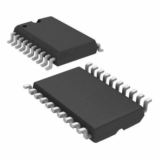
| 产品图片 |
|
| 产品型号 | TPIC6273DW |
| rohs | 库存产品核实请求 / 库存产品核实请求 |
| 产品系列 | TPIC |
| 产品目录页面 | |
| 供应商器件封装 | 20-SOIC |
| 其它名称 | 296-9002-5 |
| 包装 | 管件 |
| 安装类型 | 表面贴装 |
| 封装/外壳 | 20-SOIC(0.295",7.50mm 宽) |
| 工作温度 | -40°C ~ 125°C |
| 延迟时间-传播 | 625ps |
| 标准包装 | 25 |
| 独立电路 | 1 |
| 电压-电源 | 4.5 V ~ 5.5 V |
| 电流-输出高,低 | - |
| 电路 | 8:8 |
| 输出类型 | 标准 |
| 逻辑类型 | D 型透明锁存器 |


- 商务部:美国ITC正式对集成电路等产品启动337调查
- 曝三星4nm工艺存在良率问题 高通将骁龙8 Gen1或转产台积电
- 太阳诱电将投资9.5亿元在常州建新厂生产MLCC 预计2023年完工
- 英特尔发布欧洲新工厂建设计划 深化IDM 2.0 战略
- 台积电先进制程称霸业界 有大客户加持明年业绩稳了
- 达到5530亿美元!SIA预计今年全球半导体销售额将创下新高
- 英特尔拟将自动驾驶子公司Mobileye上市 估值或超500亿美元
- 三星加码芯片和SET,合并消费电子和移动部门,撤换高东真等 CEO
- 三星电子宣布重大人事变动 还合并消费电子和移动部门
- 海关总署:前11个月进口集成电路产品价值2.52万亿元 增长14.8%


PDF Datasheet 数据手册内容提取
TPIC6273 POWER LOGIC OCTAL D-TYPE LATCH SLIS011A – APRIL 1992 – REVISED OCTOBER 1995 • Low r ...1.3 W Typ DS(on) DW OR N PACKAGE • Avalanche Energy ...75 mJ (TOP VIEW) • Eight Power DMOS Transistor Outputs of CLR 1 20 VCC 250-mA Continuous Current • D1 2 19 D8 1.5-A Pulsed Current Per Output D2 3 18 D7 • Output Clamp Voltage up to 45 V DRAIN1 4 17 DRAIN8 • Low Power Consumption DRAIN2 5 16 DRAIN7 DRAIN3 6 15 DRAIN6 description DRAIN4 7 14 DRAIN5 D3 8 13 D6 The TPIC6273 is a monolithic high-voltage D4 9 12 D5 high-current power logic octal D-type latch with GND 10 11 CLK DMOS transistor outputs designed for use in systems that require relatively high load power. The device contains a built-in voltage clamp on the logic symbol† outputs for inductive transient protection. Power driver applications include relays, solenoids, and 1 other medium-current or high-voltage loads. CLR R 11 CLK C1 The TPIC6273 contains eight positive-edge- triggered D-type flip-flops with a direct clear input. 2 4 D1 1D DRAIN1 Each flip-flop features an open-drain power 3 5 D2 DRAIN2 DMOS transistor output. 8 6 D3 DRAIN3 When clear (CLR) is high, information at the D 9 7 D4 DRAIN4 inputs meeting the setup time requirements is 12 14 transferred to the DRAIN outputs on the positive- D5 DRAIN5 13 15 going edge of the clock pulse. Clock triggering D6 DRAIN6 18 16 occurs at a particular voltage level and is not D7 DRAIN7 directly related to the transition time of the 19 17 D8 DRAIN8 positive-going pulse. When the clock input (CLK) is at either the high or low level, the D input signal †This symbol is in accordance with ANSI/IEEE Standard 91-1984 has no effect at the output. An asynchronous CLR and IEC Publication 617-12. is provided to turn all eight DMOS-transistor FUNCTION TABLE outputs off. (each channel) The TPIC6273 is characterized for operation over INPUTS OUTPUT the operating case temperature range of –40°C CLR CLK D DRAIN to 125°C. L X X H H ↑ H L H ↑ L H H L X Latched H = high level, L = low level, X = irrelevant PRODUCTION DATA information is current as of publication date. Copyright 1995, Texas Instruments Incorporated Products conform to specifications per the terms of Texas Instruments standard warranty. Production processing does not necessarily include testing of all parameters. POST OFFICE BOX 655303 • DALLAS, TEXAS 75265 1
TPIC6273 POWER LOGIC OCTAL D-TYPE LATCH SLIS011A – APRIL 1992 – REVISED OCTOBER 1995 logic diagram (positive logic) 4 DRAIN1 1 CLR R 2 D1 1D 11 CLK C1 5 DRAIN2 R 3 D2 1D C1 6 DRAIN3 R 8 D3 1D C1 7 DRAIN4 R 9 D4 1D C1 14 DRAIN5 R 12 D5 1D C1 15 DRAIN6 R 13 D6 1D C1 16 DRAIN7 R 18 D7 1D C1 17 DRAIN8 R 19 D8 1D 10 C1 GND 2 POST OFFICE BOX 655303 • DALLAS, TEXAS 75265
TPIC6273 POWER LOGIC OCTAL D-TYPE LATCH SLIS011A – APRIL 1992 – REVISED OCTOBER 1995 schematic of inputs and outputs EQUIVALENT OF EACH INPUT TYPICAL OF ALL DRAIN OUTPUTS VCC DRAIN 45 V Input 25 V 12 V 12 V GND GND absolute maximum ratings over recommended operating case temperature range (unless otherwise noted)† Logic supply voltage, V (see Note 1) . . . . . . . . . . . . . . . . . . . . . . . . . . . . . . . . . . . . . . . . . . . . . . . . . . . . . . . 7 V CC Logic input voltage range, V . . . . . . . . . . . . . . . . . . . . . . . . . . . . . . . . . . . . . . . . . . . . . . . . . . . . . . . . –0.3 V to 7 V I Power DMOS drain-to-source voltage, V (see Note 2) . . . . . . . . . . . . . . . . . . . . . . . . . . . . . . . . . . . . . . . 45 V DS Continuous source-drain diode anode current . . . . . . . . . . . . . . . . . . . . . . . . . . . . . . . . . . . . . . . . . . . . . . . . . . 1 A Pulsed source-drain diode anode current . . . . . . . . . . . . . . . . . . . . . . . . . . . . . . . . . . . . . . . . . . . . . . . . . . . . . . 2 A Pulsed drain current, each output, all outputs on, IDn, TA = 25°C (see Note 3) . . . . . . . . . . . . . . . . . . . 750 mA Continuous drain current, each output, all outputs on, IDn, TA = 25°C . . . . . . . . . . . . . . . . . . . . . . . . . . 250 mA Peak drain current single output, IDM,TA = 25°C (see Note 3) . . . . . . . . . . . . . . . . . . . . . . . . . . . . . . . . . . . . . 2 A Single-pulse avalanche energy, EAS (see Figure 4) . . . . . . . . . . . . . . . . . . . . . . . . . . . . . . . . . . . . . . . . . . . 75 mJ Avalanche current, IAS (see Note 4) . . . . . . . . . . . . . . . . . . . . . . . . . . . . . . . . . . . . . . . . . . . . . . . . . . . . . . . . . . 1 A Continuous total power dissipation . . . . . . . . . . . . . . . . . . . . . . . . . . . . . . . . . . . . . See Dissipation Rating Table Operating virtual junction temperature range, T . . . . . . . . . . . . . . . . . . . . . . . . . . . . . . . . . . . . –40°C to 150°C J Storage temperature range, T . . . . . . . . . . . . . . . . . . . . . . . . . . . . . . . . . . . . . . . . . . . . . . . . . . –65°C to 150°C stg Lead temperature 1,6 mm (1/16 inch) from case for 10 seconds . . . . . . . . . . . . . . . . . . . . . . . . . . . . . . 260°C †Stresses beyond those listed under “absolute maximum ratings” may cause permanent damage to the device. These are stress ratings only, and functional operation of the device at these or any other conditions beyond those indicated under “recommended operating conditions” is not implied. Exposure to absolute-maximum-rated conditions for extended periods may affect device reliability. NOTES: 1. All voltage values are with respect to GND. 2. Each power DMOS source is internally connected to GND. 3. Pulse duration ≤ 100 m s, duty cycle ≤ 2% 4. DRAIN supply voltage = 15 V, starting junction temperature (TJS) = 25°C, L = 100 mH, IAS = 1 A (see Figure 4). DISSIPATION RATING TABLE TA ≤ 25°C DERATING FACTOR TA = 125°C PACKAGE POWER RATING ABOVE TA = 25°C POWER RATING DW 1125 mW 9.0 mW/°C 225 mW N 1150 mW 9.2 mW/°C 230 mW POST OFFICE BOX 655303 • DALLAS, TEXAS 75265 3
TPIC6273 POWER LOGIC OCTAL D-TYPE LATCH SLIS011A – APRIL 1992 – REVISED OCTOBER 1995 recommended operating conditions over recommended operating temperature range (unless otherwise noted) MIN MAX UNIT Logic supply voltage, VCC 4.5 5.5 V High-level input voltage, VIH 0.85 VCC V Low-level input voltage, VIL 0.15 VCC V Pulsed drain output current, TC = 25°C, VCC = 5 V (see Notes 3 and 5) –1.8 1.5 A Setup time, D high before CLK↑, tsu (see Figure 2) 10 ns Hold time, D high after CLK↑, th (see Figure 2) 15 ns Pulse duration, tw (see Figure 2) 25 ns Operating case temperature, TC –40 125 °C electrical characteristics, VCC = 5 V, TC = 25°C (unless otherwise noted) PARAMETER TEST CONDITIONS MIN TYP MAX UNIT V(BR)DSX Drain-source breakdown voltage ID = 1 mA 45 V VSD Source-drain diode forward voltage IF = 250 mA, See Note 3 0.85 1 V IIH High-level input current VCC = 5.5 V, VI = VCC 1 m A IIL Low-level input current VCC = 5.5 V, VI = 0 –1 m A ICC Logic supply current IO = 0, All inputs low 15 100 m A VDS(on) = 0.5 V, IN Nominal current IN = ID, TC = 85°C See Notes 5, 6, and 7 250 mA VDS = 40 V 0.05 1 IIDDSSXX OOffff-ssttaattee ddrraaiinn ccuurrrreenntt mm AA VDS = 40 V, TC = 125°C 0.15 5 ID = 250 mA, VCC = 4.5 V 1.3 2 rDS(on) Sretsaitsicta dnrcaein-source on-state IVDC =C 2=5 04 .m5 AV, TC = 125°C, Sanede FNigouterse s5 8a nadn d6 9 2 3.2 W ID = 500 mA, VCC = 4.5 V 1.3 2 switching characteristics, V = 5 V, T = 25°C CC C PARAMETER TEST CONDITIONS MIN TYP MAX UNIT tPLH Propagation delay time, low-to-high-level output from CLK 625 ns tPHL Propagation delay time, high-to-low-level output from CLK CLL = 30 pF,, IDD = 250 mA,, 150 ns tr Rise time, drain output See Figures 1, 2, and 10 675 ns tf Fall time, drain output 400 ns ta Reverse-recovery-current rise time IFF = 250 mA, di/dt = 20 A/mm s, 100 nnss trr Reverse-recovery time See Notes 5 and 6 and Figure 3 300 NOTES: 3. Pulse duration ≤ 100 m s, duty cycle ≤ 2% 5. Technique should limit TJ – TC to 10°C maximum. 6. These parameters are measured with voltage-sensing contacts separate from the current-carrying contacts. 7. Nominal current is defined for a consistent comparison between devices from different sources. It is the current that produces a voltage drop of 0.5 V at TC = 85°C. thermal resistance PARAMETER TEST CONDITIONS MIN MAX UNIT DW package 111 RRqq JJAA TThheerrmmaall rreessiissttaannccee, jjuunnccttiioonn-ttoo-aammbbiieenntt AAllll 88 oouuttppuuttss wwiitthh eeqquuaall ppoowweerr °°CC//WW N package 108 4 POST OFFICE BOX 655303 • DALLAS, TEXAS 75265
TPIC6273 POWER LOGIC OCTAL D-TYPE LATCH SLIS011A – APRIL 1992 – REVISED OCTOBER 1995 PARAMETER MEASUREMENT INFORMATION 5 V 24 V 5 V 20 CLK VCC ID 0 V 11 DUT RL = 95 W 5 V CLK 4–7, D Output 14–17 0 V Word DRAIN Generator D 5 V (see Note A) 1 CL = 30 pF CLR CLR (see Note B) 0 V GND 24 V 10 Output 0.5 V TEST CIRCUIT VOLTAGE WAVEFORMS Figure 1. Resistive Load Normal Operation 5 V D 5 V 0 V 5 V CLK 20 1 24 V 50% 50% 0 V Word VCC CLR ID tPLH tPHL Generator D 95 W 24 V (see Note A) DUT 90% 90% Output 10% 10% 4–7, Output 0.5 V Word 14–17 11 DRAIN tr tf Generator CLK (see Note A) SWITCHING TIMES CL = 30 pF GND (see Note B) 10 5 V CLK 50% 0 V TEST CIRCUIT tsu th 5 V D 50% 50% 0 V tw INPUT SETUP AND HOLD WAVEFORMS Figure 2. Test Circuit, Switching Times, and Voltage Waveforms NOTES: A. The word generator has the following characteristics: tr ≤ 10 ns, tf ≤ 10 ns, tw = 300 ns, pulsed repetition rate (PRR) = 5 KHz, ZO = 50 W . B. CL includes probe and jig capacitance. POST OFFICE BOX 655303 • DALLAS, TEXAS 75265 5
TPIC6273 POWER LOGIC OCTAL D-TYPE LATCH SLIS011A – APRIL 1992 – REVISED OCTOBER 1995 PARAMETER MEASUREMENT INFORMATION TP K DRAIN 0.25 A Circuit 2500 m F Under 250 V di/dt = 20 A/m s Test + IF L = 1 mH 25 V IF – (see Note B) 0 TP A t2 25% of IRM t1 t3 Driver IRM RG VGG 50 W ta (see Note A) trr CURRENT WAVEFORM TEST CIRCUIT NOTES: A. The VGG amplitude and RG are adjusted for di/dt = 20 A/m s. A VGG double-pulse train is used to set IF = 0.25 A, where t1 = 10 m s, t2 = 7 m s, and t3 = 3 m s. B. The DRAIN terminal under test is connected to the TP K test point. All other terminals are connected together and connected to the TP A test point. Figure 3. Reverse-Recovery-Current Test Circuit and Waveforms of Source-Drain Diode 5 V 15 V tw tav† 20 5 V Input VCC 0.11 W 1 CLR ID See Note B 0 V IAS = 1 A 11 DUT 100 mH Word CLK ID 4–7, Generator 14–17 (see Note A) D DRAIN VDS V(BR)DSX = 45 V GND VDS MIN 10 Input TEST CIRCUIT VOLTAGE AND CURRENT WAVEFORMS †Non-JEDEC symbol for avalanche ftime. NOTES: A. The word generator A has the following characteristics: tr ≤ 10 ns, tf ≤ 10 ns, ZO = 50 W . B. Input pulse duration, tw, is increased until peak current IAS = 1 A. Energy test is defined as EAS = IAS x V(BR)DSX x tav/2 = 75 mJ, where tav = avalanche time. Figure 4. Single-Pulse Avalanche Energy Test Circuit and Waveforms 6 POST OFFICE BOX 655303 • DALLAS, TEXAS 75265
TPIC6273 POWER LOGIC OCTAL D-TYPE LATCH SLIS011A – APRIL 1992 – REVISED OCTOBER 1995 TYPICAL CHARACTERISTICS MAXIMUM CONTINUOUS DRAIN CURRENT OF EACH OUTPUT PEAK AVALANCHE CURRENT vs vs NUMBER OF OUTPUTS CONDUCTING TIME DURATION OF AVALANCHE SIMULTANEOUSLY 10 800 TJS = 25°C ent 700 VCC = 5 V A r – 4 ur ent n C 600 ak Avalanche Curr 21 m Continuous Draiach Output – mA 453000000 TA = 25°C e uE I – PAS 00..42 – Maximof 200 TA = 125°C TA = 100°C D 100 I 0.1 0 0.1 0.2 0.4 1 2 4 10 0 1 2 3 4 5 6 7 8 tav – Time Duration of Avalanche – ms N – Number of Outputs Conducting Simultaneously Figure 5 Figure 6 MAXIMUM PEAK DRAIN CURRENT OF EACH OUTPUT vs NUMBER OF OUTPUTS CONDUCTING SIMULTANEOUSLY 2 VCC = 5 V TA = 25°C d = tw/tperiod A = 1 ms/tperiod nt – 1.5 e r r u C d = 5% n ai r 1 D k a Pe d = 50% d = 10% – D I 0.5 d = 80% 0 0 1 2 3 4 5 6 7 8 N – Number of Outputs Conducting Simultaneously Figure 7 POST OFFICE BOX 655303 • DALLAS, TEXAS 75265 7
TPIC6273 POWER LOGIC OCTAL D-TYPE LATCH SLIS011A – APRIL 1992 – REVISED OCTOBER 1995 TYPICAL CHARACTERISTICS STATIC DRAIN-SOURCE STATIC DRAIN-SOURCE ON-STATE RESISTANCE ON-STATE RESISTANCE vs vs DRAIN CURRENT LOGIC SUPPLY VOLTAGE W– 4 W– 3 ce VCC = 5 V ce ID = 250 mA an 3.5 See Note A an TC = 125 °C See Note A st st 2.5 si si e e R 3 R ate TC = 125 °C ate 2 St 2.5 St On- On- TC = 25 °C e e c 2 c 1.5 r r u u o o n-S 1.5 TC = 25 °C n-S ai ai 1 r r D D c 1 c TC = –40 °C Stati TC = – 40 °C Stati 0.5 – 0.5 – n) n) o o S( 0 S( 0 D 0.25 0.5 0.75 1 1.25 1.5 D 3 4 5 6 7 r r ID – Drain Current – A VCC – Logic Supply Voltage – V Figure 8 Figure 9 SWITCHING TIME vs FREE-AIR TEMPERATURE 700 tr 600 tPLH s ID = 250 mA n 500 – See Note A me tf Ti g 400 n hi c wit 300 S 200 tPHL 100 – 50 0 50 100 150 TA – Free-Air Temperature – °C Figure 10 NOTE A: Technique should limit TJ – TC to 10°C maximum. 8 POST OFFICE BOX 655303 • DALLAS, TEXAS 75265
PACKAGE OPTION ADDENDUM www.ti.com 29-Dec-2015 PACKAGING INFORMATION Orderable Device Status Package Type Package Pins Package Eco Plan Lead/Ball Finish MSL Peak Temp Op Temp (°C) Device Marking Samples (1) Drawing Qty (2) (6) (3) (4/5) TPIC6273DW ACTIVE SOIC DW 20 25 Green (RoHS CU NIPDAU Level-1-260C-UNLIM -40 to 125 TPIC6273 & no Sb/Br) TPIC6273DWG4 ACTIVE SOIC DW 20 25 Green (RoHS CU NIPDAU Level-1-260C-UNLIM TPIC6273 & no Sb/Br) TPIC6273DWR ACTIVE SOIC DW 20 2000 Green (RoHS CU NIPDAU Level-1-260C-UNLIM -40 to 125 TPIC6273 & no Sb/Br) TPIC6273DWRG4 ACTIVE SOIC DW 20 2000 Green (RoHS CU NIPDAU Level-1-260C-UNLIM TPIC6273 & no Sb/Br) TPIC6273N ACTIVE PDIP N 20 20 Pb-Free CU NIPDAU N / A for Pkg Type -40 to 125 TPIC6273N (RoHS) (1) The marketing status values are defined as follows: ACTIVE: Product device recommended for new designs. LIFEBUY: TI has announced that the device will be discontinued, and a lifetime-buy period is in effect. NRND: Not recommended for new designs. Device is in production to support existing customers, but TI does not recommend using this part in a new design. PREVIEW: Device has been announced but is not in production. Samples may or may not be available. OBSOLETE: TI has discontinued the production of the device. (2) Eco Plan - The planned eco-friendly classification: Pb-Free (RoHS), Pb-Free (RoHS Exempt), or Green (RoHS & no Sb/Br) - please check http://www.ti.com/productcontent for the latest availability information and additional product content details. TBD: The Pb-Free/Green conversion plan has not been defined. Pb-Free (RoHS): TI's terms "Lead-Free" or "Pb-Free" mean semiconductor products that are compatible with the current RoHS requirements for all 6 substances, including the requirement that lead not exceed 0.1% by weight in homogeneous materials. Where designed to be soldered at high temperatures, TI Pb-Free products are suitable for use in specified lead-free processes. Pb-Free (RoHS Exempt): This component has a RoHS exemption for either 1) lead-based flip-chip solder bumps used between the die and package, or 2) lead-based die adhesive used between the die and leadframe. The component is otherwise considered Pb-Free (RoHS compatible) as defined above. Green (RoHS & no Sb/Br): TI defines "Green" to mean Pb-Free (RoHS compatible), and free of Bromine (Br) and Antimony (Sb) based flame retardants (Br or Sb do not exceed 0.1% by weight in homogeneous material) (3) MSL, Peak Temp. - The Moisture Sensitivity Level rating according to the JEDEC industry standard classifications, and peak solder temperature. (4) There may be additional marking, which relates to the logo, the lot trace code information, or the environmental category on the device. (5) Multiple Device Markings will be inside parentheses. Only one Device Marking contained in parentheses and separated by a "~" will appear on a device. If a line is indented then it is a continuation of the previous line and the two combined represent the entire Device Marking for that device. Addendum-Page 1
PACKAGE OPTION ADDENDUM www.ti.com 29-Dec-2015 (6) Lead/Ball Finish - Orderable Devices may have multiple material finish options. Finish options are separated by a vertical ruled line. Lead/Ball Finish values may wrap to two lines if the finish value exceeds the maximum column width. Important Information and Disclaimer:The information provided on this page represents TI's knowledge and belief as of the date that it is provided. TI bases its knowledge and belief on information provided by third parties, and makes no representation or warranty as to the accuracy of such information. Efforts are underway to better integrate information from third parties. TI has taken and continues to take reasonable steps to provide representative and accurate information but may not have conducted destructive testing or chemical analysis on incoming materials and chemicals. TI and TI suppliers consider certain information to be proprietary, and thus CAS numbers and other limited information may not be available for release. In no event shall TI's liability arising out of such information exceed the total purchase price of the TI part(s) at issue in this document sold by TI to Customer on an annual basis. Addendum-Page 2
PACKAGE MATERIALS INFORMATION www.ti.com 14-Feb-2019 TAPE AND REEL INFORMATION *Alldimensionsarenominal Device Package Package Pins SPQ Reel Reel A0 B0 K0 P1 W Pin1 Type Drawing Diameter Width (mm) (mm) (mm) (mm) (mm) Quadrant (mm) W1(mm) TPIC6273DWR SOIC DW 20 2000 330.0 24.4 10.8 13.3 2.7 12.0 24.0 Q1 PackMaterials-Page1
PACKAGE MATERIALS INFORMATION www.ti.com 14-Feb-2019 *Alldimensionsarenominal Device PackageType PackageDrawing Pins SPQ Length(mm) Width(mm) Height(mm) TPIC6273DWR SOIC DW 20 2000 350.0 350.0 43.0 PackMaterials-Page2
None
PACKAGE OUTLINE DW0020A SOIC - 2.65 mm max height SCALE 1.200 SOIC C 10.63 SEATING PLANE TYP 9.97 A PIN 1 ID 0.1 C AREA 18X 1.27 20 1 13.0 2X 12.6 11.43 NOTE 3 10 11 0.51 20X 7.6 0.31 2.65 MAX B 7.4 0.25 C A B NOTE 4 0.33 TYP 0.10 0.25 SEE DETAIL A GAGE PLANE 0.3 1.27 0 - 8 0.1 0.40 DETAIL A TYPICAL 4220724/A 05/2016 NOTES: 1. All linear dimensions are in millimeters. Dimensions in parenthesis are for reference only. Dimensioning and tolerancing per ASME Y14.5M. 2. This drawing is subject to change without notice. 3. This dimension does not include mold flash, protrusions, or gate burrs. Mold flash, protrusions, or gate burrs shall not exceed 0.15 mm per side. 4. This dimension does not include interlead flash. Interlead flash shall not exceed 0.43 mm per side. 5. Reference JEDEC registration MS-013. www.ti.com
EXAMPLE BOARD LAYOUT DW0020A SOIC - 2.65 mm max height SOIC 20X (2) SYMM 1 20 20X (0.6) 18X (1.27) SYMM (R0.05) TYP 10 11 (9.3) LAND PATTERN EXAMPLE SCALE:6X SOOPLEDNEINRG MASK METAL MSOELTDAEL RU NMDAESRK SOOPLEDNEINRG MASK 0.07 MAX 0.07 MIN ALL AROUND ALL AROUND NON SOLDER MASK SOLDER MASK DEFINED DEFINED SOLDER MASK DETAILS 4220724/A 05/2016 NOTES: (continued) 6. Publication IPC-7351 may have alternate designs. 7. Solder mask tolerances between and around signal pads can vary based on board fabrication site. www.ti.com
EXAMPLE STENCIL DESIGN DW0020A SOIC - 2.65 mm max height SOIC 20X (2) SYMM 1 20 20X (0.6) 18X (1.27) SYMM 10 11 (9.3) SOLDER PASTE EXAMPLE BASED ON 0.125 mm THICK STENCIL SCALE:6X 4220724/A 05/2016 NOTES: (continued) 8. Laser cutting apertures with trapezoidal walls and rounded corners may offer better paste release. IPC-7525 may have alternate design recommendations. 9. Board assembly site may have different recommendations for stencil design. www.ti.com
IMPORTANTNOTICEANDDISCLAIMER TIPROVIDESTECHNICALANDRELIABILITYDATA(INCLUDINGDATASHEETS),DESIGNRESOURCES(INCLUDINGREFERENCE DESIGNS),APPLICATIONOROTHERDESIGNADVICE,WEBTOOLS,SAFETYINFORMATION,ANDOTHERRESOURCES“ASIS” ANDWITHALLFAULTS,ANDDISCLAIMSALLWARRANTIES,EXPRESSANDIMPLIED,INCLUDINGWITHOUTLIMITATIONANY IMPLIEDWARRANTIESOFMERCHANTABILITY,FITNESSFORAPARTICULARPURPOSEORNON-INFRINGEMENTOFTHIRD PARTYINTELLECTUALPROPERTYRIGHTS. TheseresourcesareintendedforskilleddevelopersdesigningwithTIproducts.Youaresolelyresponsiblefor(1)selectingtheappropriate TIproductsforyourapplication,(2)designing,validatingandtestingyourapplication,and(3)ensuringyourapplicationmeetsapplicable standards,andanyothersafety,security,orotherrequirements.Theseresourcesaresubjecttochangewithoutnotice.TIgrantsyou permissiontousetheseresourcesonlyfordevelopmentofanapplicationthatusestheTIproductsdescribedintheresource.Other reproductionanddisplayoftheseresourcesisprohibited.NolicenseisgrantedtoanyotherTIintellectualpropertyrightortoanythird partyintellectualpropertyright.TIdisclaimsresponsibilityfor,andyouwillfullyindemnifyTIanditsrepresentativesagainst,anyclaims, damages,costs,losses,andliabilitiesarisingoutofyouruseoftheseresources. TI’sproductsareprovidedsubjecttoTI’sTermsofSale(www.ti.com/legal/termsofsale.html)orotherapplicabletermsavailableeitheron ti.comorprovidedinconjunctionwithsuchTIproducts.TI’sprovisionoftheseresourcesdoesnotexpandorotherwisealterTI’sapplicable warrantiesorwarrantydisclaimersforTIproducts. MailingAddress:TexasInstruments,PostOfficeBox655303,Dallas,Texas75265 Copyright©2019,TexasInstrumentsIncorporated