
 Datasheet下载
- 型号: M74LCX16373DTR2G
- 制造商: ON Semiconductor
- 库位|库存: xxxx|xxxx
- 要求:
| 数量阶梯 | 香港交货 | 国内含税 |
| +xxxx | $xxxx | ¥xxxx |
查看当月历史价格
查看今年历史价格
M74LCX16373DTR2G产品简介:
ICGOO电子元器件商城为您提供M74LCX16373DTR2G由ON Semiconductor设计生产,在icgoo商城现货销售,并且可以通过原厂、代理商等渠道进行代购。 M74LCX16373DTR2G价格参考¥3.36-¥4.20。ON SemiconductorM74LCX16373DTR2G封装/规格:逻辑 - 锁销, D-Type Transparent Latch 2 Channel 8:8 IC Tri-State 48-TSSOP。您可以下载M74LCX16373DTR2G参考资料、Datasheet数据手册功能说明书,资料中有M74LCX16373DTR2G 详细功能的应用电路图电压和使用方法及教程。
M74LCX16373DTR2G 是一款由 ON Semiconductor 提供的逻辑锁存器(Latch)芯片,属于 74 系列 CMOS 逻辑器件。该型号的具体应用场景包括但不限于以下领域:

 1. 数据存储与传输
   - 该器件包含多个 D 型锁存器,适用于需要临时存储或缓冲数据的应用场景,例如在微处理器、微控制器和外围设备之间的数据传输过程中作为中间缓存。
   - 可用于 FIFO(先入先出)或 LIFO(后入先出)数据结构的设计。

 2. 工业控制
   - 在工业自动化系统中,该芯片可以用于输入/输出信号的锁存与控制,例如 PLC(可编程逻辑控制器)中的信号处理。
   - 适用于多路开关选择、状态保持以及信号同步等功能。

 3. 通信接口
   - 用于串行到并行、并行到串行的数据转换,支持通信协议中的数据格式化和信号处理。
   - 在 UART、SPI 或 I2C 接口设计中,可以作为数据暂存或同步单元。

 4. 显示驱动
   - 在 LED 或 LCD 显示屏的驱动电路中,该芯片可用于锁存显示数据,确保屏幕刷新时数据的一致性。
   - 特别适用于需要多路数据输入和输出的显示控制系统。

 5. 音频与视频处理
   - 在音视频设备中,可作为数据缓冲器,用于同步音频采样或视频帧数据的传输。
   - 支持对多通道信号的锁存和分配。

 6. 汽车电子
   - 在车载系统中,可用于传感器信号的采集与锁存,或者在 CAN 总线通信中作为数据缓冲单元。
   - 满足汽车电子对可靠性和稳定性的要求。

 7. 消费电子产品
   - 应用于家用电器、游戏机、打印机等设备中,用于信号的暂存、分发和同步。
   - 支持低功耗设计,适合电池供电设备。

 8. 测试与测量设备
   - 在示波器、信号发生器等测试仪器中,可用于信号的捕捉与存储,确保数据采集的准确性。
   - 适用于高速数据采集系统中的同步控制。

总结来说,M74LCX16373DTR2G 的主要应用场景集中在需要数据锁存、信号缓冲和同步的领域,广泛应用于工业、通信、消费电子和汽车等行业。其高可靠性、低功耗和多功能特性使其成为许多复杂系统设计的理想选择。
| 参数 | 数值 |
| 产品目录 | 集成电路 (IC)半导体 |
| 描述 | IC LATCH TRANSP 16BIT 48TSSOP闭锁 1.8/2.5/3.3 16-Bit Transparent |
| 产品分类 | |
| 品牌 | ON Semiconductor |
| 产品手册 | |
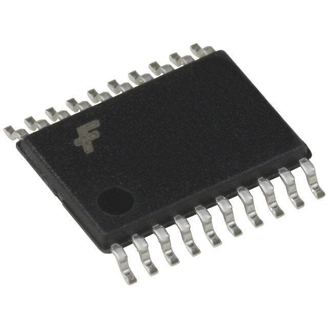
| 产品图片 |
|
| rohs | 符合RoHS无铅 / 符合限制有害物质指令(RoHS)规范要求 |
| 产品系列 | 逻辑集成电路,闭锁,ON Semiconductor M74LCX16373DTR2G74LCX |
| 数据手册 | |
| 产品型号 | M74LCX16373DTR2G |
| 产品种类 | 闭锁 |
| 传播延迟时间 | 5.9 ns at 2.7 V, 5.4 ns at 3.3 V |
| 低电平输出电流 | 32 mA |
| 供应商器件封装 | 48-TSSOP |
| 其它名称 | M74LCX16373DTR2GOSCT |
| 包装 | 剪切带 (CT) |
| 商标 | ON Semiconductor |
| 安装类型 | 表面贴装 |
| 安装风格 | SMD/SMT |
| 封装 | Reel |
| 封装/外壳 | 48-TFSOP(0.240",6.10mm 宽) |
| 封装/箱体 | TSSOP-48 |
| 工作温度 | -55°C ~ 125°C |
| 工厂包装数量 | 2500 |
| 延迟时间-传播 | 5.4ns |
| 最大工作温度 | + 85 C |
| 最小工作温度 | - 40 C |
| 极性 | Non-Inverting |
| 标准包装 | 1 |
| 独立电路 | 2 |
| 电压-电源 | 2 V ~ 3.6 V |
| 电流-输出高,低 | 24mA,24mA |
| 电源电压-最大 | 3.6 V |
| 电源电压-最小 | 2 V |
| 电路 | 8:8 |
| 电路数量 | 1 Circuit |
| 系列 | MC74LCX16373 |
| 输入线路数量 | 16 Line |
| 输出类型 | 三态 |
| 输出线路数量 | 3 Line |
| 逻辑类型 | Transparent Latch |
| 逻辑系列 | 74LCX |
| 高电平输出电流 | - 24 mA |


- 商务部:美国ITC正式对集成电路等产品启动337调查
- 曝三星4nm工艺存在良率问题 高通将骁龙8 Gen1或转产台积电
- 太阳诱电将投资9.5亿元在常州建新厂生产MLCC 预计2023年完工
- 英特尔发布欧洲新工厂建设计划 深化IDM 2.0 战略
- 台积电先进制程称霸业界 有大客户加持明年业绩稳了
- 达到5530亿美元!SIA预计今年全球半导体销售额将创下新高
- 英特尔拟将自动驾驶子公司Mobileye上市 估值或超500亿美元
- 三星加码芯片和SET,合并消费电子和移动部门,撤换高东真等 CEO
- 三星电子宣布重大人事变动 还合并消费电子和移动部门
- 海关总署:前11个月进口集成电路产品价值2.52万亿元 增长14.8%


PDF Datasheet 数据手册内容提取
MC74LCX16373 Low-Voltage CMOS 16-Bit Transparent Latch With 5 V−Tolerant Inputs and Outputs (3−State, Non−Inverting) http://onsemi.com The MC74LCX16373 is a high performance, non−inverting 16−bit transparent latch operating from a 2.3 V to 3.6 V supply. The device is byte controlled. Each byte has separate Output Enable and Latch Enable inputs. These control pins can be tied together for full 16−bit operation. 48 High impedance TTL compatible inputs significantly reduce current 1 loading to input drivers while TTL compatible outputs offer improved TSSOP−48 switching noise performance. A V specification of 5.5 V allows I DT SUFFIX MC74LCX16373 inputs to be safely driven from 5.0 V devices. CASE 1201 The MC74LCX16373 contains 16 D−type latches with 3−state 5.0 V−tolerant outputs. When the Latch Enable (LEn) inputs are HIGH, MARKING DIAGRAM data on the Dn inputs enters the latches. In this condition, the latches are transparent, i.e., a latch output will change state each time its D input 48 changes. When LE is LOW, the latches store the information that was present on the D inputs a setup time preceding the HIGH−to−LOW transition of LE. The 3−state outputs are controlled by the Output LCX16373G AWLYYWW Enable (OEn) inputs. When OE is LOW, the outputs are enabled. When OE is HIGH, the standard outputs are in the high impedance state, but this does not interfere with new data entering into the latches. 1 Features A = Assembly Location • Designed for 2.3 to 3.6 V V Operation WL = Wafer Lot CC • YY = Year 5.4 ns Maximum t pd WW = Work Week • 5.0 V Tolerant − Interface Capability With 5.0 V TTL Logic G = Pb−Free Package • Supports Live Insertion and Withdrawal • I Specification Guarantees High Impedance When V = 0 V ORDERING INFORMATION OFF CC • See detailed ordering and shipping information in the package LVTTL Compatible dimensions section on page 3 of this data sheet. • LVCMOS Compatible • 24 mA Balanced Output Sink and Source Capability • Near Zero Static Supply Current in All Three Logic States (20 (cid:2)A) Substantially Reduces System Power Requirements • Latchup Performance Exceeds 500 mA • ESD Performance: ♦ Human Body Model >2000 V ♦ Machine Model >200 V • These Devices are Pb−Free, Halogen Free/BFR Free and are RoHS Compliant © Semiconductor Components Industries, LLC, 2012 1 Publication Order Number: October, 2012 − Rev. 11 MC74LCX16373/D
MC74LCX16373 1 24 OE1 OE2 OE1 1 48 LE1 48 25 O0 2 47 D0 LE1 LE2 O1 3 46 D1 nLE 2 nLE 13 47 Q O0 36 Q O8 GND 4 45 GND D0 D D8 D O2 5 44 D2 O3 6 43 D3 nLE 3 nLE 14 46 Q O1 35 Q O9 VCC 7 42 VCC D1 D D9 D O4 8 41 D4 O5 9 40 D5 nLE 5 nLE 16 44 Q O2 33 Q O10 GND 10 39 GND D2 D D10 D O6 11 38 D6 nLE 6 nLE 17 O7 12 37 D7 43 Q O3 32 Q O11 O8 13 36 D8 D3 D D11 D O9 14 35 D9 nLE 8 nLE 19 GND 15 34 GND 41 Q O4 30 Q O12 D4 D D12 D O10 16 33 D10 O11 17 32 D11 nLE 9 nLE 20 VCC 18 31 VCC 40 Q O5 29 Q O13 D5 D D13 D O12 19 30 D12 O13 20 29 D13 nLE 11 nLE 22 GND 21 28 GND 38 Q O6 27 Q O14 D6 D D14 D O14 22 27 D14 O15 23 26 D15 nLE 12 nLE 23 OE2 24 25 LE2 37 Q O7 26 Q O15 D7 D D15 D Figure 1. Pinout: 48−Lead Figure 2. Logic Diagram (Top View) Table 1. PIN NAMES Pins Function OEn Output Enable Inputs LEn Latch Enable Inputs D0−D15 Inputs O0−O15 Outputs TRUTH TABLE Inputs Outputs Inputs Outputs LE1 OE1 D0:7 O0:7 LE2 OE2 D8:15 O8:15 X H X Z X H X Z H L L L H L L L H L H H H L H H L L X O0 L L X O0 H= High Voltage Level L= Low Voltage Level Z= High Impedance State X= High or Low Voltage Level and Transitions Are Acceptable; for ICC reasons, DO NOT FLOAT Inputs http://onsemi.com 2
MC74LCX16373 ORDERING INFORMATION Device Package Shipping† MC74LCX16373DTG TSSOP−48 39 Units / Rail (Pb−Free) M74LCX16373DTR2G TSSOP−48 2500 / Tape & Reel (Pb−Free) †For information on tape and reel specifications, including part orientation and tape sizes, please refer to our Tape and Reel Packaging Specifications Brochure, BRD8011/D. MAXIMUM RATINGS Symbol Parameter Value Condition Units VCC DC Supply Voltage −0.5 to +7.0 V VI DC Input Voltage −0.5 ≤ VI ≤ +7.0 V VO DC Output Voltage −0.5 ≤ VO ≤ +7.0 Output in 3−State V −0.5 ≤ VO ≤ VCC + 0.5 Output in HIGH or LOW State. (Note 1) V IIK DC Input Diode Current −50 VI < GND mA IOK DC Output Diode Current −50 VO < GND mA +50 VO > VCC mA IO DC Output Source/Sink Current ±50 mA ICC DC Supply Current Per Supply Pin ±100 mA IGND DC Ground Current Per Ground Pin ±100 mA TSTG Storage Temperature Range −65 to +150 °C MSL Moisture Sensitivity Level 1 Stresses exceeding Maximum Ratings may damage the device. Maximum Ratings are stress ratings only. Functional operation above the Recommended Operating Conditions is not implied. Extended exposure to stresses above the Recommended Operating Conditions may affect device reliability. 1. IO absolute maximum rating must be observed. RECOMMENDED OPERATING CONDITIONS Symbol Parameter Min Typ Max Units VCC Supply Voltage V Operating 2.0 2.5, 3.3 3.6 Data Retention Only 1.5 2.5, 3.3 3.6 VI Input Voltage 0 5.5 V VO Output Voltage V (HIGH or LOW State) 0 VCC (3−State) 0 5.5 IOH HIGH Level Output Current mA VCC = 3.0 V − 3.6 V −24 VCC = 2.7 V − 3.0 V −12 VCC = 2.3 V − 2.7 V −8 IOL LOW Level Output Current mA VCC = 3.0 V − 3.6 V +24 VCC = 2.7 V − 3.0 V +12 VCC = 2.3 V − 2.7 V +8 TA Operating Free−Air Temperature −55 +125 °C (cid:3)t/(cid:3)V Input Transition Rise or Fall Rate, VIN from 0.8 V to 2.0 V, VCC = 3.0 V 0 10 ns/V http://onsemi.com 3
MC74LCX16373 DC ELECTRICAL CHARACTERISTICS TA = −55°C to +125°C Symbol Characteristic Condition Min Max Units VIH HIGH Level Input Voltage (Note 2) 2.3 V ≤ VCC ≤ 2.7 V 1.7 V 2.7 V ≤ VCC ≤ 3.6 V 2.0 VIL LOW Level Input Voltage (Note 2) 2.3 V ≤ VCC ≤ 2.7 V 0.7 V 2.7 V ≤ VCC ≤ 3.6 V 0.8 VOH HIGH Level Output Voltage 2.3 V ≤ VCC ≤ 3.6 V; IOL = 100 (cid:2)A VCC−0.2 V VCC = 2.3 V; IOH = −8 mA 1.8 VCC = 2.7 V; IOH = −12 mA 2.2 VCC = 3.0 V; IOH = −18 mA 2.4 VCC = 3.0 V; IOH = −24 mA 2.2 VOL LOW Level Output Voltage 2.3 V ≤ VCC ≤ 3.6 V; IOL = 100 (cid:2)A 0.2 V VCC = 2.3 V; IOL = 8 mA 0.6 VCC = 2.7 V; IOL = 12 mA 0.4 VCC = 3.0 V; IOL = 16 mA 0.4 VCC = 3.0 V; IOL = 24 mA 0.55 IOZ 3−State Output Current VCC = 3.6 V, VIN = VIH or VIL, ±5 (cid:2)A VOUT = 0 to 5.5 V IOFF Power Off Leakage Current VCC = 0, VIN = 5.5 V or VOUT = 5.5 V 10 (cid:2)A IIN Input Leakage Current VCC = 3.6 V, VIN = 5.5 V or GND ±5 (cid:2)A ICC Quiescent Supply Current VCC = 3.6 V, VIN = 5.5 V or GND 20 (cid:2)A (cid:3)ICC Increase in ICC per Input 2.3 ≤ VCC ≤ 3.6 V; VIH = VCC − 0.6 V 500 (cid:2)A 2. These values of VI are used to test DC electrical characteristics only. AC CHARACTERISTICS (tR = tF = 2.5 ns; CL = 50 pF; RL = 500 (cid:4)) TA = −55°C to +125°C VCC = 3.3 V ± 0.3 V VCC = 2.7 V VCC = 2.5 V ± 0.2 V CL = 50 pF CL = 50 pF CL = 30 pF Symbol Parameter Waveform Min Max Min Max Min Max Units tPLH Propagation Delay 1 1.5 5.4 1.5 5.9 1.5 6.5 ns tPHL Dn to On 1.5 5.4 1.5 5.9 1.5 6.5 tPLH Propagation Delay 3 1.5 5.5 1.5 6.4 1.5 6.6 ns tPHL LE to On 1.5 5.5 1.5 6.4 1.5 6.6 tPZH Output Enable Time to 2 1.5 6.1 1.5 6.5 1.5 7.9 ns tPZL High and Low Level 1.5 6.1 1.5 6.5 1.5 7.9 tPHZ Output Disable Time From 2 1.5 6.0 1.5 6.3 1.5 7.2 ns tPLZ High and Low Level 1.5 6.0 1.5 6.3 1.5 7.2 ts Setup Time, HIGH or LOW Dn to 3 2.5 2.5 3.0 ns LE th Hold Time, HIGH or LOW Dn to LE 3 1.5 1.5 2.0 ns tw LE Pulse Width, HIGH 3 3.0 3.0 3.5 ns tOSHL Output−to−Output Skew 1.0 ns tOSLH (Note 3) 1.0 3. Skew is defined as the absolute value of the difference between the actual propagation delay for any two separate outputs of the same device. The specification applies to any outputs switching in the same direction, either HIGH−to−LOW (tOSHL) or LOW−to−HIGH (tOSLH); parameter guaranteed by design. http://onsemi.com 4
MC74LCX16373 DYNAMIC SWITCHING CHARACTERISTICS TA = +25°C Symbol Characteristic Condition Min Typ Max Units VOLP Dynamic LOW Peak Voltage VCC = 3.3 V, CL = 50 pF, VIH = 3.3 V, VIL = 0 V 0.8 V (Note 4) VCC = 2.5 V, CL = 30 pF, VIH = 2.5 V, VIL = 0 V 0.6 VOLV Dynamic LOW Valley Voltage VCC = 3.3 V, CL = 50 pF, VIH = 3.3 V, VIL = 0 V −0.8 V (Note 4) VCC = 2.5 V, CL = 30 pF, VIH = 2.5 V, VIL = 0 V −0.6 4. Number of outputs defined as “n”. Measured with “n−1” outputs switching from HIGH−to−LOW or LOW−to−HIGH. The remaining output is measured in the LOW state. CAPACITIVE CHARACTERISTICS Symbol Parameter Condition Typical Units CIN Input Capacitance VCC = 3.3 V, VI = 0 V or VCC 7 pF COUT Output Capacitance VCC = 3.3 V, VI = 0 V or VCC 8 pF CPD Power Dissipation Capacitance 10 MHz, VCC = 3.3 V, VI = 0 V or VCC 20 pF VCC Vmi Vmi Dn 0 V tPHL tPLH VOH Vmo Vmo On VOL WAVEFORM 1 − PROPAGATION DELAYS tR = tF = 2.5 ns, 10% to 90%; f = 1 MHz; tW = 500 ns VCC OEn VCC Dn Vmi Vmi 0 V 0 V ts th tPZH tPHZ VOH VCC Vmo VHZ LEn Vmo tw Vmo On 0 V tPZL tPLZ tPLH, tPHL VOH On Vmo On Vmo VLZ VOL VOL WAVEFORM 2 − OUTPUT ENABLE AND DISABLE TIMES WAVEFORM 3 − LE to On PROPAGATION DELAYS, LE MINIMUM tR = tF = 2.5 ns, 10% to 90%; f = 1 MHz; tW = 500 ns PULSE WIDTH, Dn to LE SETUP AND HOLD TIMES tR = tF = 2.5 ns, 10% to 90%; f = 1 MHz; tW = 500 ns except when noted Figure 3. AC Waveforms Table 2. AC WAVEFORMS VCC Symbol 3.3 V ± 0.3 V 2.7 V 2.5 V ± 0.2 V Vmi 1.5 V 1.5 V VCC / 2 Vmo 1.5 V 1.5 V VCC / 2 VHZ VOL + 0.3 V VOL + 0.3 V VOL + 0.15 V VLZ VOH − 0.3 V VOH − 0.3 V VOH − 015 V http://onsemi.com 5
MC74LCX16373 VCC 6 V or VCC × 2 OPEN PULSE DUT R1 GND GENERATOR RT CL RL Figure 4. Test Circuit Table 3. TEST CIRCUIT Test Switch tPLH, tPHL Open tPZL, tPLZ 6 V at VCC = 3.3 ± 0.3 V 6 V at VCC = 2.5 ± 0.2 V Open Collector/Drain tPLH and tPHL 6 V tPZH, tPHZ GND CL= 50 pF at VCC = 3.3 ± 0.3 V or equivalent (includes jig and probe capacitance) CL= 30 pF at VCC = 2.5 ± 0.2 V or equivalent (includes jig and probe capacitance) RL= R1 = 500 (cid:4) or equivalent RT= ZOUT of pulse generator (typically 50 (cid:4)) http://onsemi.com 6
MC74LCX16373 PACKAGE DIMENSIONS TSSOP−48 DT SUFFIX CASE 1201−01 ISSUE B 48X K REF K NOTES: 0.12 (0.005) M T U S V S K1 1. DIMENSIONING AND TOLERANCING PER ÇÉÇÉÇÉ ANSI Y14.5M, 1982. 2. CONTROLLING DIMENSION: MILLIMETER. US J ÇÉJ1 ÇÉÇÉ 3. DMIOMLEDN FSLIOANSSH ,A P ARNODT RBU DSOIO NNOST O IRN CGLAUTDEE 48 25 BURRS. MOLD FLASH OR GATE BURRS T SHALL NOT EXCEED 0.15 (0.006) PER SIDE. 54 (0.010)M L −BU− N SECTION N−N 45.. DPPIMTNERRIAM REOOXEXMTTIMNCRRINSUEUUAIMSOSSLS IIN MOO NO NNAKUFT . MD S EATHBORHLEAELIEARLOS LLKS WN C BDAAOOEIRBMT N0EL EID.E N0SN I8CTDHS LI(AOIO0OUM.WN0DNB.0NE AA3 T)DFR TOAOMRTBAALR 0.2 1 24 6. RDEIMFEENRSEINOCNES OAN ALNYD. B ARE TO BE DETERMINED AT DATUM PLANE −W−. MILLIMETERS INCHES PIDINE N1T. −AV− N DAIM 1M2.I4N0 1M2A.6X0 0.M48IN8 0M.4A9X6 B 6.00 6.20 0.236 0.244 F M C −−− 1.10 −−− 0.043 D 0.05 0.15 0.002 0.006 DETAIL E 0.25 (0.010) F 0.50 0.75 0.020 0.030 G 0.50 BSC 0.0197 BSC D H 0.37 −−− 0.015 −−− C J 0.09 0.20 0.004 0.008 −W− J1 0.09 0.16 0.004 0.006 0.076 (0.003) K 0.17 0.27 0.007 0.011 −T− SEATING DETAIL E KL1 07..1975 08..2235 00..030173 00..030295 PLANE G H M 0 (cid:2) 8 (cid:2) 0 (cid:2) 8 (cid:2) RECOMMENDED SOLDERING FOOTPRINT 48X 48X 0.32 1.00 8.45 1 0.50 PITCH DIMENSIONS: MILLIMETERS ON Semiconductor and are registered trademarks of Semiconductor Components Industries, LLC (SCILLC). SCILLC owns the rights to a number of patents, trademarks, copyrights, trade secrets, and other intellectual property. A listing of SCILLC’s product/patent coverage may be accessed at www.onsemi.com/site/pdf/Patent−Marking.pdf. SCILLC reserves the right to make changes without further notice to any products herein. SCILLC makes no warranty, representation or guarantee regarding the suitability of its products for any particular purpose, nor does SCILLC assume any liability arising out of the application or use of any product or circuit, and specifically disclaims any and all liability, including without limitation special, consequential or incidental damages. “Typical” parameters which may be provided in SCILLC data sheets and/or specifications can and do vary in different applications and actual performance may vary over time. All operating parameters, including “Typicals” must be validated for each customer application by customer’s technical experts. SCILLC does not convey any license under its patent rights nor the rights of others. SCILLC products are not designed, intended, or authorized for use as components in systems intended for surgical implant into the body, or other applications intended to support or sustain life, or for any other application in which the failure of the SCILLC product could create a situation where personal injury or death may occur. Should Buyer purchase or use SCILLC products for any such unintended or unauthorized application, Buyer shall indemnify and hold SCILLC and its officers, employees, subsidiaries, affiliates, and distributors harmless against all claims, costs, damages, and expenses, and reasonable attorney fees arising out of, directly or indirectly, any claim of personal injury or death associated with such unintended or unauthorized use, even if such claim alleges that SCILLC was negligent regarding the design or manufacture of the part. SCILLC is an Equal Opportunity/Affirmative Action Employer. This literature is subject to all applicable copyright laws and is not for resale in any manner. PUBLICATION ORDERING INFORMATION LITERATURE FULFILLMENT: N. American Technical Support: 800−282−9855 Toll Free ON Semiconductor Website: www.onsemi.com Literature Distribution Center for ON Semiconductor USA/Canada P.O. Box 5163, Denver, Colorado 80217 USA Europe, Middle East and Africa Technical Support: Order Literature: http://www.onsemi.com/orderlit Phone: 303−675−2175 or 800−344−3860 Toll Free USA/Canada Phone: 421 33 790 2910 Fax: 303−675−2176 or 800−344−3867 Toll Free USA/Canada Japan Customer Focus Center For additional information, please contact your local Email: orderlit@onsemi.com Phone: 81−3−5817−1050 Sales Representative http://onsemi.com MC74LCX16373/D 7
Mouser Electronics Authorized Distributor Click to View Pricing, Inventory, Delivery & Lifecycle Information: O N Semiconductor: M74LCX16373DTR2G MC74LCX16373DTG