 Datasheet下载
- 型号: TPIC6A259NE
- 制造商: Texas Instruments
- 库位|库存: xxxx|xxxx
- 要求:
| 数量阶梯 | 香港交货 | 国内含税 |
| +xxxx | $xxxx | ¥xxxx |
查看当月历史价格
查看今年历史价格
TPIC6A259NE产品简介:
ICGOO电子元器件商城为您提供TPIC6A259NE由Texas Instruments设计生产,在icgoo商城现货销售,并且可以通过原厂、代理商等渠道进行代购。 TPIC6A259NE价格参考¥13.12-¥26.77。Texas InstrumentsTPIC6A259NE封装/规格:逻辑 - 锁销, D-Type, Addressable 1 Channel 1:8 IC DMOS 20-PDIP。您可以下载TPIC6A259NE参考资料、Datasheet数据手册功能说明书,资料中有TPIC6A259NE 详细功能的应用电路图电压和使用方法及教程。
TPIC6A259NE 是 Texas Instruments(德州仪器)生产的一款逻辑器件,属于锁销(Latches)类集成电路。该芯片是一款高性能、高电压、高电流的达林顿晶体管阵列驱动器,内部集成了8个达林顿对管,具备较高的输出电流能力和良好的抗干扰性能。

主要应用场景包括:

1. 工业控制设备:适用于PLC(可编程逻辑控制器)、继电器控制模块、工业自动化系统等,用于驱动继电器、指示灯、小型电机等负载。

2. 显示驱动:可用于LED显示屏、数码管等显示设备的驱动电路,尤其是需要高电流驱动能力的场合。

3. 汽车电子系统:如车灯控制、仪表盘指示灯驱动、车载显示设备等,因其具备较高的可靠性和抗干扰能力,适合汽车环境。

4. 家电控制:用于洗衣机、空调、微波炉等家用电器中的电机控制、风扇控制或LED显示驱动。

5. 测试与测量设备:在测试仪器中用于控制外部负载或接口设备的驱动。

该芯片具有输出使能控制端,支持数据锁存功能,适用于需要稳定输出状态的数字控制场合。同时其耐压和输出电流能力较强,适合中高功率负载的控制应用。
| 参数 | 数值 |
| 产品目录 | 集成电路 (IC)半导体 |
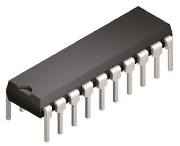
| 描述 | IC 8-BIT ADDRESSABLE LATCH20-DIP闭锁 8bit Addressable |
| 产品分类 | |
| 品牌 | Texas Instruments |
| 产品手册 | |
| 产品图片 |
|
| rohs | 符合RoHS无铅 / 符合限制有害物质指令(RoHS)规范要求 |
| 产品系列 | 逻辑集成电路,闭锁,Texas Instruments TPIC6A259NETPIC |
| 数据手册 | |
| 产品型号 | TPIC6A259NE |
| 产品目录页面 | |
| 产品种类 | 闭锁 |
| 传播延迟时间 | 125 ns at 5 V |
| 供应商器件封装 | 20-PDIP |
| 其它名称 | 296-9005-5 |
| 包装 | 管件 |
| 商标 | Texas Instruments |
| 安装类型 | 通孔 |
| 安装风格 | Through Hole |
| 封装 | Tube |
| 封装/外壳 | 20-DIP(0.300",7.62mm) |
| 封装/箱体 | PDIP-20 |
| 工作温度 | -40°C ~ 125°C |
| 工厂包装数量 | 20 |
| 延迟时间-传播 | 30ns |
| 最大工作温度 | + 125 C |
| 最小工作温度 | - 40 C |
| 极性 | Non-Inverting |
| 标准包装 | 20 |
| 独立电路 | 1 |
| 电压-电源 | 4.5 V ~ 5.5 V |
| 电流-输出高,低 | - |
| 电源电压-最大 | 5.5 V |
| 电源电压-最小 | 4.5 V |
| 电路 | 1:8 |
| 电路数量 | 1 Circuit |
| 系列 | TPIC6A259 |
| 输入线路数量 | 1 Line |
| 输出类型 | DMOS |
| 输出线路数量 | 8 Line |
| 逻辑类型 | D 型,可寻址 |


- 商务部:美国ITC正式对集成电路等产品启动337调查
- 曝三星4nm工艺存在良率问题 高通将骁龙8 Gen1或转产台积电
- 太阳诱电将投资9.5亿元在常州建新厂生产MLCC 预计2023年完工
- 英特尔发布欧洲新工厂建设计划 深化IDM 2.0 战略
- 台积电先进制程称霸业界 有大客户加持明年业绩稳了
- 达到5530亿美元!SIA预计今年全球半导体销售额将创下新高
- 英特尔拟将自动驾驶子公司Mobileye上市 估值或超500亿美元
- 三星加码芯片和SET,合并消费电子和移动部门,撤换高东真等 CEO
- 三星电子宣布重大人事变动 还合并消费电子和移动部门
- 海关总署:前11个月进口集成电路产品价值2.52万亿元 增长14.8%


PDF Datasheet 数据手册内容提取
(cid:23) (cid:1)(cid:2)(cid:3)(cid:4)(cid:5)(cid:6)(cid:7)(cid:8)(cid:9) (cid:2)(cid:10)(cid:11)(cid:12)(cid:13)(cid:14)(cid:15)(cid:10)(cid:16)(cid:3)(cid:4)(cid:14)(cid:17)(cid:18)(cid:19)(cid:3)(cid:1)(cid:14)(cid:6)(cid:20)(cid:20)(cid:13)(cid:12)(cid:21)(cid:21)(cid:6)(cid:19)(cid:15)(cid:12)(cid:14)(cid:15)(cid:6)(cid:1)(cid:4)(cid:22) (cid:23) SLIS004B − APRIL 1993 − REVISED SEPTEMBER 1995 • Low rDS(on)...1 Ω Typ NE PACKAGE • Output Short-Circuit Protection (TOP VIEW) • Avalanche Energy...75 mJ • DRAIN2 1 20 DRAIN1 Eight 350-mA DMOS Outputs DRAIN3 2 19 DRAIN0 • 50-V Switching Capability S1 3 18 S0 • Four Distinct Function Modes LGND 4 17 VCC • PGND 5 16 PGND Low Power Consumption PGND 6 15 PGND S2 7 14 CLR description G 8 13 D This power logic 8-bit addressable latch controls DRAIN4 9 12 DRAIN7 open-drain DMOS-transistor outputs and is DRAIN5 10 11 DRAIN6 designed for general-purpose storage appli- cations in digital systems. Specific uses include DW PACKAGE working registers, serial-holding registers, and (TOP VIEW) decoders or demultiplexers. This is a multi- DRAIN2 1 24 DRAIN1 functional device capable of operating as eight DRAIN3 2 23 DRAIN0 addressable latches or an 8-line demultiplexer S1 3 22 S0 with active-low DMOS outputs. Each open-drain DMOS transistor features an independent LGND 4 21 VCC chopping current-limiting circuit to prevent PGND 5 20 PGND damage in the case of a short circuit. PGND 6 19 PGND PGND 7 18 PGND Four distinct modes of operation are selectable by PGND 8 17 PGND controlling the clear (CLR) and enable (G) inputs S2 9 16 CLR as enumerated in the function table. In the G 10 15 D addressable-latch mode, data at the data-in (D) DRAIN4 11 14 DRAIN7 terminal is written into the addressed latch. The DRAIN5 12 13 DRAIN6 addressed DMOS-transistor output inverts the data input with all unaddressed DMOS-transistor FUNCTION TABLE outputs remaining in their previous states. In the memory mode, all DMOS-transistor outputs INPUTS OUTPUT OF EACH ADDRESSED OTHER FUNCTION remain in their previous states and are unaffected CLR G D DRAIN DRAIN by the data or address inputs. To eliminate the H L H L Qio Addressable possibility of entering erroneous data in the latch, H L L H Qio Latch enable G should be held high (inactive) while the H H X Qio Qio Memory address lines are changing. In the 8-line L L H L H 8-Line demultiplexing mode, the addressed output is L L L H H Demultiplexer inverted with respect to the D input and all other L H X H H Clear outputs are high. In the clear mode, all outputs are high and unaffected by the address and data LATCH SELECTION TABLE inputs. SELECT INPUTS DRAIN S2 S1 S0 ADDRESSED Separate power ground (PGND) and logic ground L L L 0 (LGND) terminals are provided to facilitate L L H 1 maximum system flexibility. All PGND terminals L H L 2 are internally connected, and each PGND L H H 3 terminal must be externally connected to the H L L 4 power system ground in order to minimize H L H 5 parasitic impedance. A single-point connection H H L 6 H H H 7 between LGND and PGND must be made externally in a manner that reduces crosstalk between the logic and load circuits. (cid:2)(cid:13)(cid:10)(cid:20)(cid:24)(cid:4)(cid:1)(cid:3)(cid:10)(cid:25) (cid:20)(cid:6)(cid:1)(cid:6) (cid:26)(cid:27)(cid:28)(cid:29)(cid:30)(cid:31)!"(cid:26)(cid:29)(cid:27) (cid:26)# $%(cid:30)(cid:30)&(cid:27)" !# (cid:29)(cid:28) ’%()(cid:26)$!"(cid:26)(cid:29)(cid:27) *!"&+ Copyright 1995, Texas Instruments Incorporated (cid:2)(cid:30)(cid:29)*%$"# $(cid:29)(cid:27)(cid:28)(cid:29)(cid:30)(cid:31) "(cid:29) #’&$(cid:26)(cid:28)(cid:26)$!"(cid:26)(cid:29)(cid:27)# ’&(cid:30) ",& "&(cid:30)(cid:31)# (cid:29)(cid:28) (cid:1)&-!# (cid:3)(cid:27)#"(cid:30)%(cid:31)&(cid:27)"# #"!(cid:27)*!(cid:30)* .!(cid:30)(cid:30)!(cid:27)"/+ (cid:2)(cid:30)(cid:29)*%$"(cid:26)(cid:29)(cid:27) ’(cid:30)(cid:29)$&##(cid:26)(cid:27)0 *(cid:29)&# (cid:27)(cid:29)" (cid:27)&$&##!(cid:30)(cid:26))/ (cid:26)(cid:27)$)%*& "&#"(cid:26)(cid:27)0 (cid:29)(cid:28) !)) ’!(cid:30)!(cid:31)&"&(cid:30)#+ POST OFFICE BOX 655303 • DALLAS, TEXAS 75265 1 • POST OFFICE BOX 1443 HOUSTON, TEXAS 77251−1443
(cid:1)(cid:2)(cid:3)(cid:4)(cid:5)(cid:6)(cid:7)(cid:8)(cid:9) (cid:23) (cid:2)(cid:10)(cid:11)(cid:12)(cid:13)(cid:14)(cid:15)(cid:10)(cid:16)(cid:3)(cid:4)(cid:14)(cid:17)(cid:18)(cid:19)(cid:3)(cid:1)(cid:14)(cid:6)(cid:20)(cid:20)(cid:13)(cid:12)(cid:21)(cid:21)(cid:6)(cid:19)(cid:15)(cid:12)(cid:14)(cid:15)(cid:6)(cid:1)(cid:4)(cid:22) (cid:23) SLIS004B − APRIL 1993 − REVISED SEPTEMBER 1995 description (continued) The TPIC6A259 is offered in a thermally-enhanced dual-in-line (NE) package and a wide-body, surface-mount (DW) package. The TPIC6A259 is characterized for operation over the operating case temperature range of −40°C to 125°C. logic symbol† S0 0 S1 8M 0 7 S2 2 G G8 D Z9 CLR Z10 9,0D DRAIN0 10,0R 9,1D DRAIN1 10,1R 9,2D DRAIN2 10,2R 9,3D DRAIN3 10,3R 9,4D DRAIN4 10,4R 9,5D DRAIN5 10,5R 9,6D DRAIN6 10,6R 9,7D DRAIN7 10,7R †This symbol is in accordance with ANSI/IEEE Std 91-1984 and IEC Publication 617-12. 2 POST OFFICE BOX 65•5303 • DALLAS, TEXAS 75265 POST OFFICE BOX 1443 HOUSTON, TEXAS 77251−1443
(cid:23) (cid:1)(cid:2)(cid:3)(cid:4)(cid:5)(cid:6)(cid:7)(cid:8)(cid:9) (cid:2)(cid:10)(cid:11)(cid:12)(cid:13)(cid:14)(cid:15)(cid:10)(cid:16)(cid:3)(cid:4)(cid:14)(cid:17)(cid:18)(cid:19)(cid:3)(cid:1)(cid:14)(cid:6)(cid:20)(cid:20)(cid:13)(cid:12)(cid:21)(cid:21)(cid:6)(cid:19)(cid:15)(cid:12)(cid:14)(cid:15)(cid:6)(cid:1)(cid:4)(cid:22) (cid:23) SLIS004B − APRIL 1993 − REVISED SEPTEMBER 1995 logic diagram (positive logic) D CLR G DRAIN0 D S0 C1 CLR DRAIN1 D C1 CLR DRAIN2 S1 D C1 CLR mp DRAIN3 u P e g D ar h C1 C d CLR n a mit DRAIN4 Li nt S2 D e r r C1 Cu CLR DRAIN5 D C1 CLR DRAIN6 D C1 CLR DRAIN7 D C1 CLR PGND POST OFFICE BOX 65•5303 • DALLAS, TEXAS 75265 3 POST OFFICE BOX 1443 HOUSTON, TEXAS 77251−1443
(cid:1)(cid:2)(cid:3)(cid:4)(cid:5)(cid:6)(cid:7)(cid:8)(cid:9) (cid:23) (cid:2)(cid:10)(cid:11)(cid:12)(cid:13)(cid:14)(cid:15)(cid:10)(cid:16)(cid:3)(cid:4)(cid:14)(cid:17)(cid:18)(cid:19)(cid:3)(cid:1)(cid:14)(cid:6)(cid:20)(cid:20)(cid:13)(cid:12)(cid:21)(cid:21)(cid:6)(cid:19)(cid:15)(cid:12)(cid:14)(cid:15)(cid:6)(cid:1)(cid:4)(cid:22) (cid:23) SLIS004B − APRIL 1993 − REVISED SEPTEMBER 1995 schematic of inputs and outputs EQUIVALENT OF EACH INPUT TYPICAL OF ALL DRAIN OUTPUTS VCC DRAIN Input 25 V 12 V RSENSE LGND LGND PGND absolute maximum ratings over the recommended operating case temperature range (unless otherwise noted)† Logic supply voltage, V (see Note 1) . . . . . . . . . . . . . . . . . . . . . . . . . . . . . . . . . . . . . . . . . . . . . . . . . . . . . . . 7 V CC Logic input voltage range, V . . . . . . . . . . . . . . . . . . . . . . . . . . . . . . . . . . . . . . . . . . . . . . . . . . . . . . . . −0.3 V to 7 V I Power DMOS drain-to-source voltage, V (see Note 2) . . . . . . . . . . . . . . . . . . . . . . . . . . . . . . . . . . . . . . . 50 V DS Continuous source-to-drain diode anode current . . . . . . . . . . . . . . . . . . . . . . . . . . . . . . . . . . . . . . . . . . . . . . . . 1 A Pulsed source-to-drain diode anode current (see Note 3) . . . . . . . . . . . . . . . . . . . . . . . . . . . . . . . . . . . . . . . . . 2 A Pulsed drain current, each output, all outputs on, ID, TC = 25°C (see Note 3) . . . . . . . . . . . . . . . . . . . . . 1.1 A Continuous drain current, each output, all outputs on, ID, TC = 25°C . . . . . . . . . . . . . . . . . . . . . . . . . . . 350 mA Peak drain current single output, TC = 25°C (see Note 3) . . . . . . . . . . . . . . . . . . . . . . . . . . . . . . . . . . . . . . 1.1 A Single-pulse avalanche energy, EAS (see Figure 6) . . . . . . . . . . . . . . . . . . . . . . . . . . . . . . . . . . . . . . . . . . 75 mJ Avalanche current, IAS (see Note 4) . . . . . . . . . . . . . . . . . . . . . . . . . . . . . . . . . . . . . . . . . . . . . . . . . . . . . . 600 mA Continuous total dissipation . . . . . . . . . . . . . . . . . . . . . . . . . . . . . . . . . . . . . . . . . . . See Dissipation Rating Table Operating virtual junction temperature range, T . . . . . . . . . . . . . . . . . . . . . . . . . . . . . . . . . . . . . −40°C to 150°C J Operating case temperature range, T . . . . . . . . . . . . . . . . . . . . . . . . . . . . . . . . . . . . . . . . . . . . . −40°C to 125°C C Storage temperature range, T . . . . . . . . . . . . . . . . . . . . . . . . . . . . . . . . . . . . . . . . . . . . . . . . . . . −65°C to 150°C stg Lead temperature 1,6 mm (1/16 inch) from case for 10 seconds . . . . . . . . . . . . . . . . . . . . . . . . . . . . . . 260°C †Stresses beyond those listed under “absolute maximum ratings” may cause permanent damage to the device. These are stress ratings only, and functional operation of the device at these or any other conditions beyond those indicated under “recommended operating conditions” is not implied. Exposure to absolute-maximum-rated conditions for extended periods may affect device reliability. NOTES: 1. All voltage values are with respect to LGND and PGND. 2. Each power DMOS source is internally connected to PGND. 3. Pulse duration ≤ 100 µs, and duty cycle ≤ 2%. 4. DRAIN supply voltage = 15 V, starting junction temperature (TJS) = 25°C, L = 210 mH, and IAS = 600 mA (see Figure 6). DISSIPATION RATING TABLE TC ≤ 25°C DERATING FACTOR TC = 125°C PACKAGE POWER RATING ABOVE TC = 25°C POWER RATING DW 1750 mW 14 mW/°C 350 mW NE 2500 mW 20 mW/°C 500 mW 4 POST OFFICE BOX 65•5303 • DALLAS, TEXAS 75265 POST OFFICE BOX 1443 HOUSTON, TEXAS 77251−1443
(cid:23) (cid:1)(cid:2)(cid:3)(cid:4)(cid:5)(cid:6)(cid:7)(cid:8)(cid:9) (cid:2)(cid:10)(cid:11)(cid:12)(cid:13)(cid:14)(cid:15)(cid:10)(cid:16)(cid:3)(cid:4)(cid:14)(cid:17)(cid:18)(cid:19)(cid:3)(cid:1)(cid:14)(cid:6)(cid:20)(cid:20)(cid:13)(cid:12)(cid:21)(cid:21)(cid:6)(cid:19)(cid:15)(cid:12)(cid:14)(cid:15)(cid:6)(cid:1)(cid:4)(cid:22) (cid:23) SLIS004B − APRIL 1993 − REVISED SEPTEMBER 1995 recommended operating conditions MIN MAX UNIT Logic supply voltage, VCC 4.5 5.5 V High-level input voltage, VIH 0.85 VCC VCC V Low-level input voltage, VIL 0 0.15 VCC V Pulsed drain output current, TC = 25°C, VCC = 5 V (see Notes 3 and 5) −1.8 0.6 A Setup time, D high before G↑,tsu (see Figure 2) 10 ns Hold time, D high before G↑, th (see Figure 2) 5 ns Pulse duration, tw (see Figure 2) 15 ns Operating case temperature, TC −40 125 °C electrical characteristics, VCC = 5 V, TC = 25°C (unless otherwise noted) PARAMETER TEST CONDITIONS MIN TYP MAX UNIT V(BR)DSX Drain-to-source breakdown voltage ID = 1 mA 50 V Source-to-drain diode forward VSD voltage IF = 350 mA, See Note 3 0.8 1.1 V IIH High-level input current VI = VCC 1 µA IIL Low-level input current VI = 0 −1 µA ICC Logic supply current IO = 0, VI = VCC or 0 0.5 5 mA Output current at which chopping IOK starts TC = 25°C, See Note 5 and Figures 3 and 4 0.6 0.8 1.1 A VDS(on) = 0.5 V, I(nom) = ID, TC = 85°C, I(nom) Nominal current VCC = 5 V, See Notes 5, 6, and 7 350 mA VDS = 40 V, TC = 25°C 0.1 1 IIDD OOffff--ssttaattee ddrraaiinn ccuurrrreenntt VDS = 40 V, TC = 125°C 0.2 5 µAA SSttaattiicc ddrraaiinn--ttoo--ssoouurrccee oonn--ssttaattee ID = 350 mA, TC = 25°C SSeeee NNootteess 55 aanndd 66 1 1.5 rrDDSS((oonn)) resistance ID = 350 mA, TC = 125°C and Figures 9 and 10 1.7 2.5 ΩΩ switching characteristics, VCC = 5 V, TC = 25°C PARAMETER TEST CONDITIONS MIN TYP MAX UNIT tPHL Propagation delay time, high- to low-level output from D 30 ns tPLH Propagation delay time, low- to high-level output from D CCLL == 3300 ppFF,, IIDD == 335500 mmAA,, 125 ns tr Rise time, drain output SSeeee FFiigguurreess 11,, 22,, aanndd 1111 60 ns tf Fall time, drain output 30 ns ta Reverse-recovery-current rise time IIFF == 335500 mmAA,, ddii//ddtt == 2200 AA//µµss,, 100 ns trr Reverse-recovery time See Notes 5 and 6 and Figure 5 300 ns NOTES: 3. Pulse duration ≤ 100 µs and duty cycle ≤ 2%. 5. Technique should limit TJ − TC to 10°C maximum. 6. These parameters are measured with voltage-sensing contacts separate from the current-carrying contacts. 7. Nominal current is defined for a consistent comparison between devices from different sources. It is the current that produces a voltage drop of 0.5 V at TC = 85°C. thermal resistance PARAMETER TEST CONDITIONS MIN MAX UNIT DW 10 RRθJJCC TThheerrmmaall rreessiissttaannccee,, jjuunnccttiioonn--ttoo--ccaassee AAllll eeiigghhtt oouuttppuuttss wwiitthh eeqquuaall ppoowweerr °°CC//WW NE 10 DW 50 RRθJJAA TThheerrmmaall rreessiissttaannccee,, jjuunnccttiioonn--ttoo--aammbbiieenntt AAllll eeiigghhtt oouuttppuuttss wwiitthh eeqquuaall ppoowweerr °°CC//WW NE 50 POST OFFICE BOX 65•5303 • DALLAS, TEXAS 75265 5 POST OFFICE BOX 1443 HOUSTON, TEXAS 77251−1443
(cid:1)(cid:2)(cid:3)(cid:4)(cid:5)(cid:6)(cid:7)(cid:8)(cid:9) (cid:23) (cid:2)(cid:10)(cid:11)(cid:12)(cid:13)(cid:14)(cid:15)(cid:10)(cid:16)(cid:3)(cid:4)(cid:14)(cid:17)(cid:18)(cid:19)(cid:3)(cid:1)(cid:14)(cid:6)(cid:20)(cid:20)(cid:13)(cid:12)(cid:21)(cid:21)(cid:6)(cid:19)(cid:15)(cid:12)(cid:14)(cid:15)(cid:6)(cid:1)(cid:4)(cid:22) (cid:23) SLIS004B − APRIL 1993 − REVISED SEPTEMBER 1995 PARAMETER MEASUREMENT INFORMATION 5 V 5 V 24 V CLR 0 V 5 V S0 S0 VCC ID 0 V S1 RL = 68 Ω S1 5 V Word S2 DUT 0 V Generator Output 5 V (see Note A) G S2 CLR DRAIN 0 V D CL = 30 pF 5 V LGND PGND G (see Note B) 0 V 5 V D 0 V 24 V TEST CIRCUIT DRAIN5 0.5 V 24 V DRAIN3 0.5 V VOLTAGE WAVEFORMS Figure 1. Typical Operation Mode 5 V 5 V G 0 V 5 V 24 V D 50% 50% VCC CLR 0 V Word tPLH tPHL Generator D ID 24 V (see Note A) Output 90% 90% DUT 68 Ω 10% 10% 0.5 V Word Output tr tf Generator G SWITCHING TIMES (see Note A) DRAIN LGND PGND 5 V CL = 30 pF G 50% (see Note B) 0 V tsu TEST CIRCUIT th 5 V D 50% 50% 0 V tw INPUT SETUP AND HOLD WAVEFORMS Figure 2. Test Circuit, Switching Times, and Voltage Waveforms NOTES: A. The word generator has the following characteristics: tr ≤ 10 ns, tf ≤ 10 ns, tw = 300 ns, pulsed repetition rate (PRR) = 5 kHz, ZO = 50 Ω. B. CL includes probe and jig capacitance. 6 POST OFFICE BOX 65•5303 • DALLAS, TEXAS 75265 POST OFFICE BOX 1443 HOUSTON, TEXAS 77251−1443
(cid:23) (cid:1)(cid:2)(cid:3)(cid:4)(cid:5)(cid:6)(cid:7)(cid:8)(cid:9) (cid:2)(cid:10)(cid:11)(cid:12)(cid:13)(cid:14)(cid:15)(cid:10)(cid:16)(cid:3)(cid:4)(cid:14)(cid:17)(cid:18)(cid:19)(cid:3)(cid:1)(cid:14)(cid:6)(cid:20)(cid:20)(cid:13)(cid:12)(cid:21)(cid:21)(cid:6)(cid:19)(cid:15)(cid:12)(cid:14)(cid:15)(cid:6)(cid:1)(cid:4)(cid:22) (cid:23) SLIS004B − APRIL 1993 − REVISED SEPTEMBER 1995 PARAMETER MEASUREMENT INFORMATION OUTPUT CURRENT vs TIME FOR INCREASING LOAD RESISTANCE REGION 1 CURRENT WAVEFORM 1.5 IOK 1.25 nt − A 1 I(aOsneKde BN)otes A urrent e C urr ut C p ut 0.75 Out − Outp 0.5 I − O I O 0 t t t t t 1 2 1 2 1 0.25 t1 ≈ 40 µs t2 ≈ 2.5 ms 0 Region 1 Region 2 Time Time First output current pulses after turn-on in chopping mode with resistive load. NOTES: A. Figure 3 illustrates the output current characteristics of the device energizing a load having initially low, increasing resistance, e.g., an incandescent lamp. In region 1, chopping occurs and the peak current is limited to IOK. In region 2, output current is continuous. The same characteristics occur in reverse order when the device energizes a load having an initially high, decreasing resistance. B. Region 1 duty cycle is approximately 2%. Figure 3. Chopping-Mode Characteristics OUTPUT CURRENT LIMIT vs CASE TEMPERATURE 1.5 VCC = 5.5 V A 1.2 − mit Li nt 0.9 re VCC = 4.5 V r u C ut p 0.6 ut O − I O 0.3 0 − 50 − 25 0 25 50 75 100 125 150 TC − Case Temperature − °C Figure 4 POST OFFICE BOX 65•5303 • DALLAS, TEXAS 75265 7 POST OFFICE BOX 1443 HOUSTON, TEXAS 77251−1443
(cid:1)(cid:2)(cid:3)(cid:4)(cid:5)(cid:6)(cid:7)(cid:8)(cid:9) (cid:23) (cid:2)(cid:10)(cid:11)(cid:12)(cid:13)(cid:14)(cid:15)(cid:10)(cid:16)(cid:3)(cid:4)(cid:14)(cid:17)(cid:18)(cid:19)(cid:3)(cid:1)(cid:14)(cid:6)(cid:20)(cid:20)(cid:13)(cid:12)(cid:21)(cid:21)(cid:6)(cid:19)(cid:15)(cid:12)(cid:14)(cid:15)(cid:6)(cid:1)(cid:4)(cid:22) (cid:23) SLIS004B − APRIL 1993 − REVISED SEPTEMBER 1995 PARAMETER MEASUREMENT INFORMATION TP K DRAIN 0.35 A Circuit 2500 µF UTnedsetr 250 V di/dt = 20 A/µs + IF L = 1 mH 24 V IF − (see Note B) 0 TP A 25% of IRM t2 t1 t3 Driver IRM RG (see Note C) VGG 50 Ω ta (see Note A) trr CURRENT WAVEFORM TEST CIRCUIT NOTES: A. The VGG amplitude and RG are adjusted for di/dt = 20 A/µs. A VGG double-pulse train is used to set IF = 0.35 A, where t1 = 10 µs, t2 = 7 µs, and t3 = 3 µs. B. The DRAIN terminal under test is connected to the TP K test point. All other terminals are connected together and connected to the TP A test point. C. IRM = maximum recovery current Figure 5. Reverse-Recovery-Current Test Circuit and Waveforms of Source-Drain Diode 5 V 15 V tw tav† VCC 5 V S2 1 Ω Input S1 ID See Note B 0 V Word S0 DUT IAS = 600 mA Generator L = 210 mH (see Note A) G ID D DRAIN VDS CLR V(BR)DSX = 50 V LGND PGND VDS MIN TEST CIRCUIT VOLTAGE AND CURRENT WAVEFORMS †Non-JEDEC symbol for avalanche time. NOTES: A. The word generator has the following characteristics: tr ≤ 10 ns, tf ≤ 10 ns, ZO = 50 Ω. B. Input pulse duration, tw, is increased until peak current IAS = 600 mA. Energy test level is defined as EAS = (IAS × V(BR)DSX × tav)/2 = 75 mJ. Figure 6. Single-Pulse Avalanche Energy Test Circuit and Waveforms 8 POST OFFICE BOX 65•5303 • DALLAS, TEXAS 75265 POST OFFICE BOX 1443 HOUSTON, TEXAS 77251−1443
(cid:23) (cid:1)(cid:2)(cid:3)(cid:4)(cid:5)(cid:6)(cid:7)(cid:8)(cid:9) (cid:2)(cid:10)(cid:11)(cid:12)(cid:13)(cid:14)(cid:15)(cid:10)(cid:16)(cid:3)(cid:4)(cid:14)(cid:17)(cid:18)(cid:19)(cid:3)(cid:1)(cid:14)(cid:6)(cid:20)(cid:20)(cid:13)(cid:12)(cid:21)(cid:21)(cid:6)(cid:19)(cid:15)(cid:12)(cid:14)(cid:15)(cid:6)(cid:1)(cid:4)(cid:22) (cid:23) SLIS004B − APRIL 1993 − REVISED SEPTEMBER 1995 TYPICAL CHARACTERISTICS MAXIMUM CONTINUOUS MAXIMUM PEAK DRAIN CURRENT DRAIN CURRENT OF EACH OUTPUT OF EACH OUTPUT vs vs NUMBER OF OUTPUTS CONDUCTING NUMBER OF OUTPUTS CONDUCTING SIMULTANEOUSLY A SIMULTANEOUSLY 0.7 ut − 0.9 nt VCC = 5 V utp 0.8 rre 0.6 h O d = 50% d = 20% ain Cu 0.5 TA = 25°C of Eac 0.7 ntinuous DrOutput − A 0.4 TA = 100°C ain Current 00..65 d = 80% Coh 0.3 Dr 0.4 ximum of Eac 0.2 m Peak 0.3 I− MaD 0.1 TA = 125°C − Maximu 00..21 VTddA C== C =1tw =2m/5 t5sp° C/eVtprieordiod M 0 D 0 1 2 3 4 5 6 7 8 I 1 2 3 4 5 6 7 8 N − Number of Outputs Conducting Simultaneously N − Number of Outputs Conducting Simultaneously Figure 7 Figure 8 STATIC DRAIN-SOURCE STATIC DRAIN-SOURCE ON-STATE RESISTANCE ON-STATE RESISTANCE vs vs DRAIN CURRENT LOGIC SUPPLY VOLTAGE Ω 2 Ω Resistance − 11.7.55 TC = 125°C VSeCeC N =o 5te V A Resistance − 1.17.255 TC = 125°C On-State 1.25 TC = 25°C Current Limit On-State 1.25 TC = 25°C Source 1 Source 1 Drain- 0.75 TC = − 40°C Drain- 0.75 TC = −40°C Static 0.5 Static 0.5 − 0.25 − 0.25 S(on) 0 S(on) 0 ISDe e= N35o0te m AA rD 0 0.2 0.4 0.6 0.8 1 1.2 rD 4 5 6 7 ID − Drain Current − A VCC − Logic Supply Voltage − V Figure 9 Figure 10 NOTE A: Technique should limit TJ − TC to 10°C maximum. POST OFFICE BOX 65•5303 • DALLAS, TEXAS 75265 9 POST OFFICE BOX 1443 HOUSTON, TEXAS 77251−1443
(cid:1)(cid:2)(cid:3)(cid:4)(cid:5)(cid:6)(cid:7)(cid:8)(cid:9) (cid:23) (cid:2)(cid:10)(cid:11)(cid:12)(cid:13)(cid:14)(cid:15)(cid:10)(cid:16)(cid:3)(cid:4)(cid:14)(cid:17)(cid:18)(cid:19)(cid:3)(cid:1)(cid:14)(cid:6)(cid:20)(cid:20)(cid:13)(cid:12)(cid:21)(cid:21)(cid:6)(cid:19)(cid:15)(cid:12)(cid:14)(cid:15)(cid:6)(cid:1)(cid:4)(cid:22) (cid:23) SLIS004B − APRIL 1993 − REVISED SEPTEMBER 1995 TYPICAL CHARACTERISTICS SWITCHING TIME vs CASE TEMPERATURE 140 ID = 350 mA See Note A 120 tPLH s n 100 − e m Ti g 80 n hi c wit 60 tr S 40 tPHL tf 20 − 50 0 50 100 150 TC − Case Temperature − °C NOTE A: Technique should limit TJ − TC to 10°C maximum. Figure 11 THERMAL INFORMATION NE PACKAGE TRANSIENT THERMAL IMPEDANCE vs The single-pulse curve represents measured data. The curves for various pulse durations are based on the following equation: ON TIME (cid:2) (cid:2) (cid:2) (cid:2) 100 Z(cid:1)JA (cid:1) ttw R(cid:1)JA (cid:3) 1– ttw Z(cid:1)(cid:4)tw(cid:3)tc(cid:5) W c c °C− / d = 50% (cid:3) Z(cid:1)(cid:4)tw(cid:5)–Z(cid:1)(cid:4)tc(cid:5) e Where: nc d = 20% mpeda 10 d = 10% Z(cid:1)(cid:4)tw(cid:5) = ftohre ts =in gtwle -speuclsoen dthsermal impedance al I d = 5% Z(cid:1)(cid:4)tc(cid:5) = the single-pulse thermal impedance m r for t = tc seconds e nt Th 1 d = 2% Z(cid:1)(cid:4)tw(cid:3)tc(cid:5) = ftohre ts =in gtwle -+p utcls see tchoenrdmsa l impedance e si an d = tw/tc Tr Z − θJA Single Pulse tw tc ID 0.1 0.001 0.01 0.1 1 10 100 1000 0 t − On Time − s Figure 12 10 POST OFFICE BOX 65•5303 • DALLAS, TEXAS 75265 POST OFFICE BOX 1443 HOUSTON, TEXAS 77251−1443
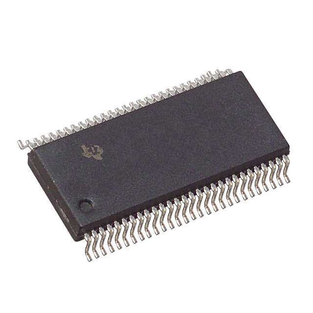
PACKAGE OPTION ADDENDUM www.ti.com 6-Feb-2020 PACKAGING INFORMATION Orderable Device Status Package Type Package Pins Package Eco Plan Lead/Ball Finish MSL Peak Temp Op Temp (°C) Device Marking Samples (1) Drawing Qty (2) (6) (3) (4/5) TPIC6A259DW ACTIVE SOIC DW 24 25 Green (RoHS NIPDAU Level-1-260C-UNLIM -40 to 125 TPIC6A259 & no Sb/Br) TPIC6A259DWG4 ACTIVE SOIC DW 24 25 Green (RoHS NIPDAU Level-1-260C-UNLIM -40 to 125 TPIC6A259 & no Sb/Br) TPIC6A259DWRG4 ACTIVE SOIC DW 24 2000 Green (RoHS NIPDAU Level-1-260C-UNLIM -40 to 125 TPIC6A259 & no Sb/Br) TPIC6A259NE ACTIVE PDIP NE 20 20 Pb-Free NIPDAU N / A for Pkg Type -40 to 125 TPIC6A259NE (RoHS) (1) The marketing status values are defined as follows: ACTIVE: Product device recommended for new designs. LIFEBUY: TI has announced that the device will be discontinued, and a lifetime-buy period is in effect. NRND: Not recommended for new designs. Device is in production to support existing customers, but TI does not recommend using this part in a new design. PREVIEW: Device has been announced but is not in production. Samples may or may not be available. OBSOLETE: TI has discontinued the production of the device. (2) RoHS: TI defines "RoHS" to mean semiconductor products that are compliant with the current EU RoHS requirements for all 10 RoHS substances, including the requirement that RoHS substance do not exceed 0.1% by weight in homogeneous materials. Where designed to be soldered at high temperatures, "RoHS" products are suitable for use in specified lead-free processes. TI may reference these types of products as "Pb-Free". RoHS Exempt: TI defines "RoHS Exempt" to mean products that contain lead but are compliant with EU RoHS pursuant to a specific EU RoHS exemption. Green: TI defines "Green" to mean the content of Chlorine (Cl) and Bromine (Br) based flame retardants meet JS709B low halogen requirements of <=1000ppm threshold. Antimony trioxide based flame retardants must also meet the <=1000ppm threshold requirement. (3) MSL, Peak Temp. - The Moisture Sensitivity Level rating according to the JEDEC industry standard classifications, and peak solder temperature. (4) There may be additional marking, which relates to the logo, the lot trace code information, or the environmental category on the device. (5) Multiple Device Markings will be inside parentheses. Only one Device Marking contained in parentheses and separated by a "~" will appear on a device. If a line is indented then it is a continuation of the previous line and the two combined represent the entire Device Marking for that device. (6) Lead/Ball Finish - Orderable Devices may have multiple material finish options. Finish options are separated by a vertical ruled line. Lead/Ball Finish values may wrap to two lines if the finish value exceeds the maximum column width. Important Information and Disclaimer:The information provided on this page represents TI's knowledge and belief as of the date that it is provided. TI bases its knowledge and belief on information provided by third parties, and makes no representation or warranty as to the accuracy of such information. Efforts are underway to better integrate information from third parties. TI has taken and Addendum-Page 1
PACKAGE OPTION ADDENDUM www.ti.com 6-Feb-2020 continues to take reasonable steps to provide representative and accurate information but may not have conducted destructive testing or chemical analysis on incoming materials and chemicals. TI and TI suppliers consider certain information to be proprietary, and thus CAS numbers and other limited information may not be available for release. In no event shall TI's liability arising out of such information exceed the total purchase price of the TI part(s) at issue in this document sold by TI to Customer on an annual basis. Addendum-Page 2
PACKAGE MATERIALS INFORMATION www.ti.com 5-Jul-2019 TAPE AND REEL INFORMATION *Alldimensionsarenominal Device Package Package Pins SPQ Reel Reel A0 B0 K0 P1 W Pin1 Type Drawing Diameter Width (mm) (mm) (mm) (mm) (mm) Quadrant (mm) W1(mm) TPIC6A259DWRG4 SOIC DW 24 2000 330.0 24.4 10.75 15.7 2.7 12.0 24.0 Q1 PackMaterials-Page1
PACKAGE MATERIALS INFORMATION www.ti.com 5-Jul-2019 *Alldimensionsarenominal Device PackageType PackageDrawing Pins SPQ Length(mm) Width(mm) Height(mm) TPIC6A259DWRG4 SOIC DW 24 2000 350.0 350.0 43.0 PackMaterials-Page2
None
IMPORTANTNOTICEANDDISCLAIMER TI PROVIDES TECHNICAL AND RELIABILITY DATA (INCLUDING DATASHEETS), DESIGN RESOURCES (INCLUDING REFERENCE DESIGNS), APPLICATION OR OTHER DESIGN ADVICE, WEB TOOLS, SAFETY INFORMATION, AND OTHER RESOURCES “AS IS” AND WITH ALL FAULTS, AND DISCLAIMS ALL WARRANTIES, EXPRESS AND IMPLIED, INCLUDING WITHOUT LIMITATION ANY IMPLIED WARRANTIES OF MERCHANTABILITY, FITNESS FOR A PARTICULAR PURPOSE OR NON-INFRINGEMENT OF THIRD PARTY INTELLECTUAL PROPERTY RIGHTS. These resources are intended for skilled developers designing with TI products. You are solely responsible for (1) selecting the appropriate TI products for your application, (2) designing, validating and testing your application, and (3) ensuring your application meets applicable standards, and any other safety, security, or other requirements. These resources are subject to change without notice. TI grants you permission to use these resources only for development of an application that uses the TI products described in the resource. Other reproduction and display of these resources is prohibited. No license is granted to any other TI intellectual property right or to any third party intellectual property right. TI disclaims responsibility for, and you will fully indemnify TI and its representatives against, any claims, damages, costs, losses, and liabilities arising out of your use of these resources. TI’s products are provided subject to TI’s Terms of Sale (www.ti.com/legal/termsofsale.html) or other applicable terms available either on ti.com or provided in conjunction with such TI products. TI’s provision of these resources does not expand or otherwise alter TI’s applicable warranties or warranty disclaimers for TI products. Mailing Address: Texas Instruments, Post Office Box 655303, Dallas, Texas 75265 Copyright © 2020, Texas Instruments Incorporated