 Datasheet下载
- 型号: TPD4S012DRYR
- 制造商: Texas Instruments
- 库位|库存: xxxx|xxxx
- 要求:
| 数量阶梯 | 香港交货 | 国内含税 |
| +xxxx | $xxxx | ¥xxxx |
查看当月历史价格
查看今年历史价格
TPD4S012DRYR产品简介:
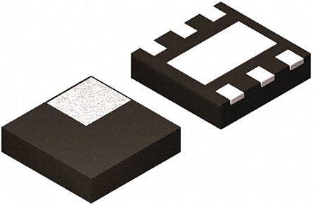
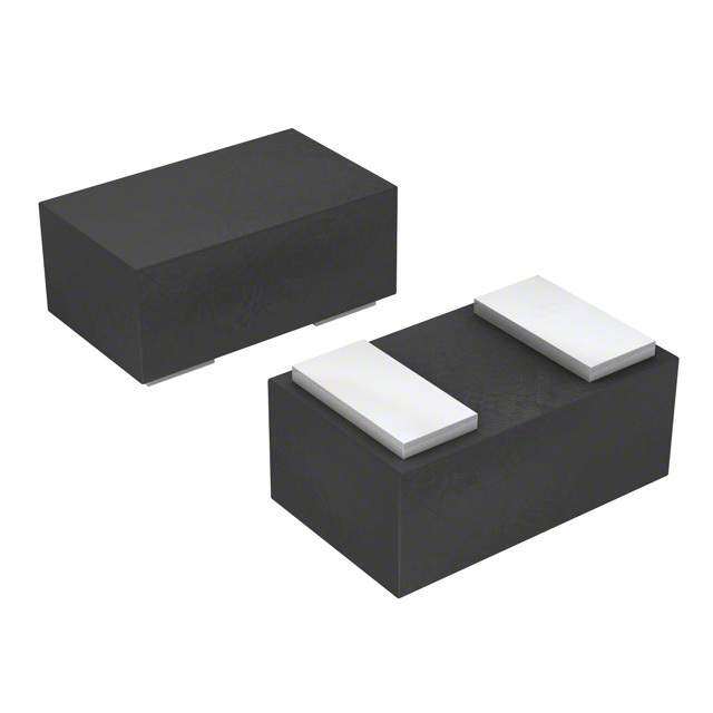
ICGOO电子元器件商城为您提供TPD4S012DRYR由Texas Instruments设计生产,在icgoo商城现货销售,并且可以通过原厂、代理商等渠道进行代购。 TPD4S012DRYR价格参考¥5.55-¥9.99。Texas InstrumentsTPD4S012DRYR封装/规格:TVS - 二极管, Clamp 3A (8/20µs) Ipp Tvs Diode Surface Mount 6-SON (1.45x1)。您可以下载TPD4S012DRYR参考资料、Datasheet数据手册功能说明书,资料中有TPD4S012DRYR 详细功能的应用电路图电压和使用方法及教程。
TPD4S012DRYR是德州仪器(Texas Instruments)推出的一款TVS(瞬态电压抑制)二极管阵列,专为高速数据接口的静电放电(ESD)保护设计。该器件采用小型化WSON-8封装,适用于对空间要求严苛的便携式电子设备。

其主要应用场景包括智能手机、平板电脑、笔记本电脑和便携式医疗设备等消费类电子产品中的高速通信接口保护。具体支持USB 2.0、HDMI、DisplayPort、音频插孔及其它高速差分信号线路,可有效防护IEC61000-4-2接触放电高达±15kV的ESD冲击,同时保持极低的电容特性(典型值0.3pF),避免影响信号完整性。

TPD4S012DRYR集成了四路ESD保护二极管,具备低钳位电压和快速响应能力,可在瞬间泄放高压脉冲,保护后端敏感集成电路。其工作温度范围为-40°C至+125°C,适合工业级和商业级应用环境。

典型应用还包括连接器接口保护,如耳机插孔、USB Type-A/C端口等,广泛用于需高可靠性与紧凑设计的终端产品中。凭借小尺寸、高性能和高集成度,TPD4S012DRYR成为现代电子设备中理想的ESD防护解决方案。
| 参数 | 数值 |
| 产品目录 | |
| 描述 | IC 4CH ESD SOLUTION W/CLAMP 6SONESD 抑制器 4Ch USB ESD Solution w/ Pwr Clamp |
| 产品分类 | |
| 品牌 | Texas Instruments |
| 产品手册 | |
| 产品图片 |
|
| rohs | 符合RoHS无铅 / 符合限制有害物质指令(RoHS)规范要求 |
| 产品系列 | Texas Instruments TPD4S012DRYR- |
| 数据手册 | |
| 产品型号 | TPD4S012DRYR |
| 产品培训模块 | http://www.digikey.cn/PTM/IndividualPTM.page?site=cn&lang=zhs&ptm=25363 |
| 产品目录页面 | |
| 产品种类 | ESD 抑制器 |
| 供应商器件封装 | 6-SON(1.45x1) |
| 其它名称 | 296-24244-1 |
| 击穿电压 | 24 V |
| 制造商产品页 | http://www.ti.com/general/docs/suppproductinfo.tsp?distId=10&orderablePartNumber=TPD4S012DRYR |
| 功率(W) | 60W |
| 包装 | 剪切带 (CT) |
| 商标 | Texas Instruments |
| 封装 | Reel |
| 封装/外壳 | 6-UFDFN |
| 封装/箱体 | USON-6 |
| 工作温度范围 | - 40 C to + 85 C |
| 工厂包装数量 | 5000 |
| 应用 | USB |
| 技术 | 混合技术 |
| 标准包装 | 1 |
| 电压-工作 | - |
| 电压-箝位 | - |
| 电容 | 0.8 pF |
| 电路数 | 4 |
| 端接类型 | SMD/SMT |
| 系列 | TPD4S012 |
| 通道 | 4 Channels |


- 商务部:美国ITC正式对集成电路等产品启动337调查
- 曝三星4nm工艺存在良率问题 高通将骁龙8 Gen1或转产台积电
- 太阳诱电将投资9.5亿元在常州建新厂生产MLCC 预计2023年完工
- 英特尔发布欧洲新工厂建设计划 深化IDM 2.0 战略
- 台积电先进制程称霸业界 有大客户加持明年业绩稳了
- 达到5530亿美元!SIA预计今年全球半导体销售额将创下新高
- 英特尔拟将自动驾驶子公司Mobileye上市 估值或超500亿美元
- 三星加码芯片和SET,合并消费电子和移动部门,撤换高东真等 CEO
- 三星电子宣布重大人事变动 还合并消费电子和移动部门
- 海关总署:前11个月进口集成电路产品价值2.52万亿元 增长14.8%


PDF Datasheet 数据手册内容提取
Product Sample & Technical Tools & Support & Folder Buy Documents Software Community TPD4S012 SLVS928B–MARCH2009–REVISEDAUGUST2014 TPD4S012 4-Channel ESD Solution for USB-HS/USB OTG/USB Charger Interface 1 Features 3 Description • IntegratedESDClampsonallPins The TPD4S012 is a four-channel Transient Voltage 1 Suppressor (TVS) based Electrostatic Discharge • USBSignalPins(D+,D–,ID) (ESD) protection diode array for USB chargers and – 0.8-pFLineCapacitance USBOn-The-Go(OTG)interfaces. • SupportsDataRatesinExcessof480Mbps The TPD4S012 provides IEC 61000-4-2 system level • IEC61000-4-2ESDProtection(Level4Contact) ESD Protection featuring 15 V tolerance on the V BUS – ±10-kVIEC61000-4-2ContactDischarge line. The device is ideal for providing circuit protection for USB charger and OTG applications due to its • IEC61000-4-5Surge high-voltagetoleranceattheV lineandsmallflow- BUS – 3AmpsPeakPulseCurrent throughpackage. 2 Applications DeviceInformation(1) • CellularPhones PARTNUMBER PACKAGE BODYSIZE(NOM) • DigitalCameras TPD4S012 SON(6) 1.45mmx1.00mm • GlobalPositioningSystems(GPS) (1) For all available packages, see the orderable addendum at theendofthedatasheet. • PortableDigitalAssistants(PDA) • PortableComputers TypicalApplicationSchematic V BUS D+ PMU/USB Controller D- ID GND 1 An IMPORTANT NOTICE at the end of this data sheet addresses availability, warranty, changes, use in safety-critical applications, intellectualpropertymattersandotherimportantdisclaimers.UNLESSOTHERWISENOTED,thisdocumentcontainsPRODUCTION DATA.
TPD4S012 SLVS928B–MARCH2009–REVISEDAUGUST2014 www.ti.com Table of Contents 1 Features.................................................................. 1 7.3 FeatureDescription..................................................8 2 Applications........................................................... 1 7.4 DeviceFunctionalModes..........................................9 3 Description............................................................. 1 8 ApplicationsandImplementation...................... 10 4 RevisionHistory..................................................... 2 8.1 ApplicationInformation............................................10 8.2 TypicalApplication..................................................10 5 PinConfigurationsandFunctions....................... 3 9 PowerSupplyRecommendations...................... 12 6 Specifications......................................................... 4 10 Layout................................................................... 12 6.1 AbsoluteMaximumRatings......................................4 6.2 HandlingRatings.......................................................4 10.1 LayoutGuidelines.................................................12 6.3 RecommendedOperatingConditions.......................4 10.2 LayoutExample....................................................12 6.4 ThermalInformation..................................................4 11 DeviceandDocumentationSupport................. 13 6.5 ElectricalCharacteristics...........................................5 11.1 Trademarks...........................................................13 6.6 TypicalCharacteristics..............................................6 11.2 ElectrostaticDischargeCaution............................13 7 DetailedDescription.............................................. 8 11.3 Glossary................................................................13 7.1 Overview...................................................................8 12 Mechanical,Packaging,andOrderable Information........................................................... 13 7.2 FunctionalBlockDiagram.........................................8 4 Revision History ChangesfromRevisionA(November2009)toRevisionB Page • AddedHandlingRatingtable,FeatureDescriptionsection,DeviceFunctionalModes,Applicationand Implementationsection,PowerSupplyRecommendationssection,Layoutsection,DeviceandDocumentation Supportsection,andMechanical,Packaging,andOrderableInformationsection ............................................................... 1 2 SubmitDocumentationFeedback Copyright©2009–2014,TexasInstrumentsIncorporated ProductFolderLinks:TPD4S012
TPD4S012 www.ti.com SLVS928B–MARCH2009–REVISEDAUGUST2014 5 Pin Configurations and Functions DRY PACKAGE (TOP VIEW) D+ 1 6 V BUS D- 2 5 N.C. ID 3 4 GND N.C.–Notinternallyconnected D+,D–,andIDpinsareexactequivalentESDclampcircuits.AnyofthesepinscanbeconnectedtoanyotherD+, D–,orIDpinifitbecomeseasiertoroutethetracesfromtheUSBconnector. PinFunctions PIN DRY TYPE DESCRIPTION NAME PINNO. 1 D+ ESDclamp ProvidesESDprotectiontothehigh-speeddifferentialdatalines 2 D– ESDclamp ProvidesESDprotectiontothehigh-speeddifferentialdatalines 3 ID ESDclamp ProvidesESDprotectiontothehigh-speeddifferentialdatalines 4 GND PWR Ground 5 N.C. – Notinternallyconnected 6 V ESDclamp ESDclampforhigh-voltagetolerantV line(s) BUS BUS Copyright©2009–2014,TexasInstrumentsIncorporated SubmitDocumentationFeedback 3 ProductFolderLinks:TPD4S012
TPD4S012 SLVS928B–MARCH2009–REVISEDAUGUST2014 www.ti.com 6 Specifications 6.1 Absolute Maximum Ratings Overoperatingfree-airtemperaturerange(unlessotherwisenoted) PARAMETER MIN MAX UNIT V voltagetolerance V pin –0.3 20 V BUS BUS IOvoltagetolerance D+,D–,IDpins –0.3 6 V T Operatingfree-airtemperaturerange –40 85 °C A IEC61000-4-2ContactDischarge D+,D–,ID ±10 kV V pin ±10 kV BUS IEC61000-4-2Air-GapDischarge D+,D–,ID ±10 kV V pin ±9 kV BUS PeakpulsePower(Allpins) 60 W IEC61000-4-5Surge(t =8/20μs) p Peakpulsecurrent(AllPins) 3 A 6.2 Handling Ratings MIN MAX UNIT T Storagetemperaturerange –65 125 °C stg Humanbodymodel(HBM),perANSI/ESDA/JEDECJS-001,all –2.5 2.5 pins(1) V Electrostaticdischarge kV (ESD) Chargeddevicemodel(CDM),perJEDECspecification –1 1 JESD22-C101,allpins(2) (1) JEDECdocumentJEP155statesthat500-VHBMallowssafemanufacturingwithastandardESDcontrolprocess. (2) JEDECdocumentJEP157statesthat250-VCDMallowssafemanufacturingwithastandardESDcontrolprocess. 6.3 Recommended Operating Conditions overoperatingfree-airtemperaturerange(unlessotherwisenoted) PARAMETER MIN MAX UNIT T Operatingfree-airTemperatureRange –40 85 °C A OperatingVoltage V Pin 0 15 V BUS D+,D–,IDPins 0 5.5 6.4 Thermal Information TPD4S012 THERMALMETRIC(1) DRY UNIT 6PINS R Junction-to-ambientthermalresistance 461.3 θJA R Junction-to-case(top)thermalresistance 219.6 θJC(top) R Junction-to-boardthermalresistance 343.7 °C/W θJB ψ Junction-to-topcharacterizationparameter 162.5 JT ψ Junction-to-boardcharacterizationparameter 343.7 JB (1) Formoreinformationabouttraditionalandnewthermalmetrics,seetheICPackageThermalMetricsapplicationreport,SPRA953. 4 SubmitDocumentationFeedback Copyright©2009–2014,TexasInstrumentsIncorporated ProductFolderLinks:TPD4S012
TPD4S012 www.ti.com SLVS928B–MARCH2009–REVISEDAUGUST2014 6.5 Electrical Characteristics overoperatingfree-airtemperaturerange(unlessotherwisenoted) PARAMETER TESTCONDITIONS MIN TYP MAX UNIT I V operatingcurrent V =19V D+,D–,IDpinsopen 0.1 0.5 μA VBUS BUS BUS V =2.5V,V = I IOportcurrent IO BUS D+,D–,IDpins 0.1 0.5 μA IO 5V V D+,D–,IDpins(lowerclamp D Diodeforwardvoltage I =8mA 0.6 0.8 0.95 V IO diode) C V pincapacitance V =5V 11 15 pF VBUS BUS BUS C IOcapacitance V =2.5V D+,D–,IDpins 0.8 1 pF IO IO D+,D–,ID,andV pins, BUS I =1.5A includingcentralclampdioded 1.2 IO duringpositiveESDpulse R Dynamicresistance Ω DYN D+,D–,ID,andV pins, BUS I =1A includingcentralclampdiode 1 IO duringnegativeESDpulse D+,D–,IDpins 6 9 V Breakdownvoltage I =1mA V BR IO V pin(s) 20 24 BUS Copyright©2009–2014,TexasInstrumentsIncorporated SubmitDocumentationFeedback 5 ProductFolderLinks:TPD4S012
TPD4S012 SLVS928B–MARCH2009–REVISEDAUGUST2014 www.ti.com 6.6 Typical Characteristics 6.0 3.5 5.5 Power 3.0 5.0 Current 4.5 2.5 4.0 A) 3.5 A) 2.0 ( 3.0 ( P P P P I 2.5 I 1.5 2.0 Power Current 1.0 1.5 1.0 0.5 0.5 0 0 0 5 10 15 20 25 30 35 40 45 50 0 5 10 15 20 25 30 35 40 45 50 Time (ms) Time (ms) Figure1.PeakPulsePowerWaveformattheD+,D–,orID Figure2.PeakPulsePowerWaveformattheV Pin BUS Pin 2.0 1.8 1.8 1.6 1.6 1.4 1.4 1.2 A)1.2 A)1.0 nt (1.0 nt ( urre0.8 urre0.8 C C 0.6 0.6 0.4 0.4 0.2 0.2 0 0 0 2 4 6 8 10 10 12 14 0 5 10 15 20 25 30 Voltage (V) Voltage (V) Figure3.D+,D–,orIDClampVoltageUnderESDEvent Figure4.V ClampVoltageUnderESDEvent BUS 1.70E-12 1.80E-11 1.60E-12 1.70E-11 1.50E-12 1.60E-11 1.40E-12 1.50E-11 1.30E-12 ds 1.40E-11 VBUSto GND a 1.20E-12 Far 1.10E-12 ads 1.30E-11 ar 1.00E-12 D+ to GND F 1.20E-11 9.00E-13 1.10E-11 8.00E-13 1.00E-11 7.00E-13 9.00E-12 0.0 1.0 2.0 3.0 4.0 5.0 0.0 1.0 2.0 3.0 4.0 5.0 Volts Volts Figure5.D+,D–,orIDCapacitance,TA=27°C Figure6.VBUSCapacitance,TA=27°C 6 SubmitDocumentationFeedback Copyright©2009–2014,TexasInstrumentsIncorporated ProductFolderLinks:TPD4S012
TPD4S012 www.ti.com SLVS928B–MARCH2009–REVISEDAUGUST2014 Typical Characteristics (continued) 140 40 120 20 100 0 80 V) V) –20 e ( 60 e ( d d u u –40 plit 40 plit m m A A –60 20 –80 0 –20 –100 –40 –120 0 25 50 75 100 125 150 175 200 225 250 0 25 50 75 100 125 150 175 200 225 250 Time (ns) Time (ns) Figure7.IECClampingWaveform,8kVContact,D+,25 Figure8.IECClampingWaveform,–8kVContact,D+,25 ns/div ns/div 140 40 120 20 100 0 80 V) V) –20 e ( 60 e ( d d u u –40 plit 40 plit m m A A –60 20 –80 0 –20 –100 –40 –120 0 25 50 75 100 125 150 175 200 225 250 0 25 50 75 100 125 150 175 200 225 250 Time (ns) Time (ns) Figure9.V IECClampingWaveform,8kVContact,25 Figure10.V IECClampingWaveform,–8kVContact,25 BUS BUS ns/div ns/div Copyright©2009–2014,TexasInstrumentsIncorporated SubmitDocumentationFeedback 7 ProductFolderLinks:TPD4S012
TPD4S012 SLVS928B–MARCH2009–REVISEDAUGUST2014 www.ti.com 7 Detailed Description 7.1 Overview The TPD4S012 is a four-channel Transient Voltage Suppressor (TVS) based Electrostatic Discharge (ESD) protectiondiodearrayforUSBchargersandUSBOn-The-Go(OTG)interfaces. The TPD4S012 provides IEC 61000-4-2 system level ESD Protection featuring 15 V tolerance on the V line. BUS The device is ideal for providing circuit protection for USB charger and OTG applications due to its high-voltage toleranceattheV lineandsmallflow-throughpackage. BUS 7.2 Functional Block Diagram V BUS D+ D– - ID GND 7.3 Feature Description 7.3.1 IntegratedESDClamps Integrated ESD Clamps on the D+, D–, V , and ID pins provide single-chip ESD protection for USB High BUS Speed,USB-OTG,andUSBchargerinterfaces. 7.3.2 USBSignalPins D+,D– andIDUSBSignalpinshavelowcapacitance(0.8pFTyp). 7.3.3 V Line BUS TheV linehasa11pF(Typ)capacitance. BUS 7.3.4 SupportsDataRatesinExcessof480Mbps Thelowcapacitance(0.8pFTyp)ofthedatalinessupportsspeedsinexcessof480Mbps. 7.3.5 IEC61000-4-2(Level4Contact) IEC 61000-4-2 (Level 4 contact) system level ESD compliance measured at the D+, D– and ID pins is rated for ±10kVcontactandair-gapdischarge. 7.3.6 IEC61000-4-5Surge IEC 61000-4-5 system level surge compliance measured at D+, D–, ID, and V pins rated to 3 A of peak pulse BUS current. 8 SubmitDocumentationFeedback Copyright©2009–2014,TexasInstrumentsIncorporated ProductFolderLinks:TPD4S012
TPD4S012 www.ti.com SLVS928B–MARCH2009–REVISEDAUGUST2014 7.4 Device Functional Modes The TPD4S012 is a passive integrated circuit that triggers when voltages are above V or below the lower BR diode's V. During ESD events, voltages as high as ±10 kV (contact) can be directed to ground via the internal f diode network. Once the voltages on the protected line fall below the trigger levels of TPD4S012 (usually within 10'sofnano-seconds),thedevicerevertstopassive. Copyright©2009–2014,TexasInstrumentsIncorporated SubmitDocumentationFeedback 9 ProductFolderLinks:TPD4S012
TPD4S012 SLVS928B–MARCH2009–REVISEDAUGUST2014 www.ti.com 8 Applications and Implementation 8.1 Application Information The TPD4S012 is a four-channel Transient Voltage Suppressor (TVS) based Electrostatic Discharge (ESD) protectiondiodearrayforUSBchargersandUSBOn-The-Go(OTG)interfaces. The TPD4S012 provides IEC 61000-4-2 system level ESD Protection featuring 15 V tolerance on the V line. BUS The device is ideal for providing circuit protection for USB charger and OTG applications due to its high-voltage toleranceattheV lineandsmallflow-throughpackage. BUS 8.2 Typical Application V BUS V BUS D+ D+ D– - D– PMU/USB ID Controller ID GND GND IftheIDpinisnotused,itcanbeleftfloating. Figure11. TypicalApplicationSchematic 8.2.1 DesignRequirements Forthisdesignexample,asingleTPD4S012isusedtoprotectallpinsofamicro/miniUSBconnector. GiventheUSBapplication,thefollowingparametersareknown. DESIGNPARAMETER VALUE SignalrangeonD+,D–,andID 0Vto5V SignalrangeonV 0Vto5V BUS OperatingFrequency 240MHz 8.2.2 DetailedDesignProcedure Tobeginthedesignprocess,someparametersmustbedecidedupon;thedesignerneedstoknowthefollowing: • Signalrangeonalltheprotectedlines • Operatingfrequency 8.2.2.1 SignalRangeonD+,D-,IDandV pins BUS The TPD4S012 has 3 pins which support 0 to 5.5 V signals, these are suited for the D+, D–, and ID pins. The V pinissuitablefortheVBUSline,andhasthebenefitofbeingtolerantofvoltagesupto16V BUS 8.2.2.2 OperatingFrequency The0.8pF(Typ)oftheTPD4S012supportdataratesinexcessof480Mbps. 10 SubmitDocumentationFeedback Copyright©2009–2014,TexasInstrumentsIncorporated ProductFolderLinks:TPD4S012
TPD4S012 www.ti.com SLVS928B–MARCH2009–REVISEDAUGUST2014 8.2.3 ApplicationCurve 140 40 120 20 100 0 80 V) V) –20 e ( 60 e ( d d u u –40 plit 40 plit m m A A –60 20 –80 0 –20 –100 –40 –120 0 25 50 75 100 125 150 175 200 225 250 0 25 50 75 100 125 150 175 200 225 250 Time (ns) Time (ns) Figure12.IECClampingWaveform,8kVContact,D+,25 Figure13.IECClampingWaveform,–8kVContact,D+,25 ns/div ns/div 140 40 120 20 100 0 80 V) V) –20 e ( 60 e ( d d u u –40 plit 40 plit m m A A –60 20 –80 0 –20 –100 –40 –120 0 25 50 75 100 125 150 175 200 225 250 0 25 50 75 100 125 150 175 200 225 250 Time (ns) Time (ns) Figure14.V IECClampingWaveform,8kVContact,25 Figure15.V IECClampingWaveform,–8kVContact, BUS BUS ns/div 25ns/div Copyright©2009–2014,TexasInstrumentsIncorporated SubmitDocumentationFeedback 11 ProductFolderLinks:TPD4S012
TPD4S012 SLVS928B–MARCH2009–REVISEDAUGUST2014 www.ti.com 9 Power Supply Recommendations This family of devices are passive ESD protection devices and there is no need to power them. Care should be taken to not violate the maximum voltage specification to ensure that the device functions properly. The V BUS TVSdiodecantolerateuptoa15Vsignal.TheD+,D–,andIDpinstolerateuptoa5.5Vsignal. 10 Layout 10.1 Layout Guidelines • Theoptimumplacementisasclosetotheconnectoraspossible. – EMI during an ESD event can couple from the trace being struck to other nearby unprotected traces, resultinginearlysystemfailures. – The PCB designer needs to minimize the possibility of EMI coupling by keeping any unprotected traces awayfromtheprotectedtraceswhicharebetweentheTVSandtheconnector. • Routetheprotectedtracesasstraightaspossible. • Eliminate any sharp corners on the protected traces between the TVS and the connector by using rounded cornerswiththelargestradiipossible. – Electricfieldstendtobuilduponcorners,increasingEMIcoupling. 10.2 Layout Example ThisapplicationistypicalofamobileUSBplatformwithanIDpininadditiontotheD+,D–,andV pins. BUS V BUS D+ 1 6 D- 2 5 ID 3 4 GND LEGEND TOP LAYER BOTTOM LAYER VIA Figure16. UsingDRYPackage 12 SubmitDocumentationFeedback Copyright©2009–2014,TexasInstrumentsIncorporated ProductFolderLinks:TPD4S012
TPD4S012 www.ti.com SLVS928B–MARCH2009–REVISEDAUGUST2014 11 Device and Documentation Support 11.1 Trademarks Alltrademarksarethepropertyoftheirrespectiveowners. 11.2 Electrostatic Discharge Caution Thesedeviceshavelimitedbuilt-inESDprotection.Theleadsshouldbeshortedtogetherorthedeviceplacedinconductivefoam duringstorageorhandlingtopreventelectrostaticdamagetotheMOSgates. 11.3 Glossary SLYZ022—TIGlossary. Thisglossarylistsandexplainsterms,acronyms,anddefinitions. 12 Mechanical, Packaging, and Orderable Information The following pages include mechanical, packaging, and orderable information. This information is the most current data available for the designated devices. This data is subject to change without notice and revision of thisdocument.Forbrowser-basedversionsofthisdatasheet,refertotheleft-handnavigation. Copyright©2009–2014,TexasInstrumentsIncorporated SubmitDocumentationFeedback 13 ProductFolderLinks:TPD4S012
PACKAGE OPTION ADDENDUM www.ti.com 6-Feb-2020 PACKAGING INFORMATION Orderable Device Status Package Type Package Pins Package Eco Plan Lead/Ball Finish MSL Peak Temp Op Temp (°C) Device Marking Samples (1) Drawing Qty (2) (6) (3) (4/5) TPD4S012DRYR ACTIVE SON DRY 6 5000 Green (RoHS NIPDAU Level-1-260C-UNLIM -40 to 85 3B & no Sb/Br) (1) The marketing status values are defined as follows: ACTIVE: Product device recommended for new designs. LIFEBUY: TI has announced that the device will be discontinued, and a lifetime-buy period is in effect. NRND: Not recommended for new designs. Device is in production to support existing customers, but TI does not recommend using this part in a new design. PREVIEW: Device has been announced but is not in production. Samples may or may not be available. OBSOLETE: TI has discontinued the production of the device. (2) RoHS: TI defines "RoHS" to mean semiconductor products that are compliant with the current EU RoHS requirements for all 10 RoHS substances, including the requirement that RoHS substance do not exceed 0.1% by weight in homogeneous materials. Where designed to be soldered at high temperatures, "RoHS" products are suitable for use in specified lead-free processes. TI may reference these types of products as "Pb-Free". RoHS Exempt: TI defines "RoHS Exempt" to mean products that contain lead but are compliant with EU RoHS pursuant to a specific EU RoHS exemption. Green: TI defines "Green" to mean the content of Chlorine (Cl) and Bromine (Br) based flame retardants meet JS709B low halogen requirements of <=1000ppm threshold. Antimony trioxide based flame retardants must also meet the <=1000ppm threshold requirement. (3) MSL, Peak Temp. - The Moisture Sensitivity Level rating according to the JEDEC industry standard classifications, and peak solder temperature. (4) There may be additional marking, which relates to the logo, the lot trace code information, or the environmental category on the device. (5) Multiple Device Markings will be inside parentheses. Only one Device Marking contained in parentheses and separated by a "~" will appear on a device. If a line is indented then it is a continuation of the previous line and the two combined represent the entire Device Marking for that device. (6) Lead/Ball Finish - Orderable Devices may have multiple material finish options. Finish options are separated by a vertical ruled line. Lead/Ball Finish values may wrap to two lines if the finish value exceeds the maximum column width. Important Information and Disclaimer:The information provided on this page represents TI's knowledge and belief as of the date that it is provided. TI bases its knowledge and belief on information provided by third parties, and makes no representation or warranty as to the accuracy of such information. Efforts are underway to better integrate information from third parties. TI has taken and continues to take reasonable steps to provide representative and accurate information but may not have conducted destructive testing or chemical analysis on incoming materials and chemicals. TI and TI suppliers consider certain information to be proprietary, and thus CAS numbers and other limited information may not be available for release. In no event shall TI's liability arising out of such information exceed the total purchase price of the TI part(s) at issue in this document sold by TI to Customer on an annual basis. Addendum-Page 1
PACKAGE MATERIALS INFORMATION www.ti.com 3-Aug-2017 TAPE AND REEL INFORMATION *Alldimensionsarenominal Device Package Package Pins SPQ Reel Reel A0 B0 K0 P1 W Pin1 Type Drawing Diameter Width (mm) (mm) (mm) (mm) (mm) Quadrant (mm) W1(mm) TPD4S012DRYR SON DRY 6 5000 179.0 8.4 1.2 1.65 0.7 4.0 8.0 Q1 TPD4S012DRYR SON DRY 6 5000 180.0 9.5 1.2 1.65 0.7 4.0 8.0 Q1 PackMaterials-Page1
PACKAGE MATERIALS INFORMATION www.ti.com 3-Aug-2017 *Alldimensionsarenominal Device PackageType PackageDrawing Pins SPQ Length(mm) Width(mm) Height(mm) TPD4S012DRYR SON DRY 6 5000 203.0 203.0 35.0 TPD4S012DRYR SON DRY 6 5000 189.0 185.0 36.0 PackMaterials-Page2
GENERIC PACKAGE VIEW DRY 6 USON - 0.6 mm max height PLASTIC SMALL OUTLINE - NO LEAD Images above are just a representation of the package family, actual package may vary. Refer to the product data sheet for package details. 4207181/G
PACKAGE OUTLINE DRY0006A USON - 0.6 mm max height SCALE 8.500 PLASTIC SMALL OUTLINE - NO LEAD B 1.05 A 0.95 PIN 1 INDEX AREA 1.5 1.4 0.6 MAX C SEATING PLANE 0.05 0.00 0.08 C 3X 0.6 SYMM (0.127) TYP (0.05) TYP 3 4 4X 0.5 SYMM 2X 1 6 1 0.25 6X 0.15 0.4 0.3 0.1 C A B 0.05 C PIN 1 ID (OPTIONAL) 0.35 5X 0.25 4222894/A 01/2018 NOTES: 1. All linear dimensions are in millimeters. Any dimensions in parenthesis are for reference only. Dimensioning and tolerancing per ASME Y14.5M. 2. This drawing is subject to change without notice. www.ti.com
EXAMPLE BOARD LAYOUT DRY0006A USON - 0.6 mm max height PLASTIC SMALL OUTLINE - NO LEAD SYMM (0.35) 5X (0.3) 1 6 6X (0.2) SYMM 4X (0.5) 4 3 (R0.05) TYP (0.6) LAND PATTERN EXAMPLE 1:1 RATIO WITH PKG SOLDER PADS EXPOSED METAL SHOWN SCALE:40X 0.05 MAX 0.05 MIN ALL AROUND ALL AROUND EXPOSED EXPOSED METAL METAL SOLDER MASK METAL METAL UNDER SOLDER MASK OPENING SOLDER MASK OPENING NON SOLDER MASK DEFINED SOLDER MASK DEFINED (PREFERRED) SOLDER MASK DETAILS 4222894/A 01/2018 NOTES: (continued) 3. For more information, see QFN/SON PCB application report in literature No. SLUA271 (www.ti.com/lit/slua271). www.ti.com
EXAMPLE STENCIL DESIGN DRY0006A USON - 0.6 mm max height PLASTIC SMALL OUTLINE - NO LEAD SYMM (0.35) 5X (0.3) 1 6 6X (0.2) SYMM 4X (0.5) 4 3 (R0.05) TYP (0.6) SOLDER PASTE EXAMPLE BASED ON 0.075 - 0.1 mm THICK STENCIL SCALE:40X 4222894/A 01/2018 NOTES: (continued) 4. Laser cutting apertures with trapezoidal walls and rounded corners may offer better paste release. IPC-7525 may have alternate design recommendations. www.ti.com
IMPORTANTNOTICEANDDISCLAIMER TI PROVIDES TECHNICAL AND RELIABILITY DATA (INCLUDING DATASHEETS), DESIGN RESOURCES (INCLUDING REFERENCE DESIGNS), APPLICATION OR OTHER DESIGN ADVICE, WEB TOOLS, SAFETY INFORMATION, AND OTHER RESOURCES “AS IS” AND WITH ALL FAULTS, AND DISCLAIMS ALL WARRANTIES, EXPRESS AND IMPLIED, INCLUDING WITHOUT LIMITATION ANY IMPLIED WARRANTIES OF MERCHANTABILITY, FITNESS FOR A PARTICULAR PURPOSE OR NON-INFRINGEMENT OF THIRD PARTY INTELLECTUAL PROPERTY RIGHTS. These resources are intended for skilled developers designing with TI products. You are solely responsible for (1) selecting the appropriate TI products for your application, (2) designing, validating and testing your application, and (3) ensuring your application meets applicable standards, and any other safety, security, or other requirements. These resources are subject to change without notice. TI grants you permission to use these resources only for development of an application that uses the TI products described in the resource. Other reproduction and display of these resources is prohibited. No license is granted to any other TI intellectual property right or to any third party intellectual property right. TI disclaims responsibility for, and you will fully indemnify TI and its representatives against, any claims, damages, costs, losses, and liabilities arising out of your use of these resources. TI’s products are provided subject to TI’s Terms of Sale (www.ti.com/legal/termsofsale.html) or other applicable terms available either on ti.com or provided in conjunction with such TI products. TI’s provision of these resources does not expand or otherwise alter TI’s applicable warranties or warranty disclaimers for TI products. Mailing Address: Texas Instruments, Post Office Box 655303, Dallas, Texas 75265 Copyright © 2020, Texas Instruments Incorporated