ICGOO在线商城 > 集成电路(IC) > 线性 - 音頻放大器 > TPA0213DGQ
 Datasheet下载
- 型号: TPA0213DGQ
- 制造商: Texas Instruments
- 库位|库存: xxxx|xxxx
- 要求:
| 数量阶梯 | 香港交货 | 国内含税 |
| +xxxx | $xxxx | ¥xxxx |
查看当月历史价格
查看今年历史价格
TPA0213DGQ产品简介:
ICGOO电子元器件商城为您提供TPA0213DGQ由Texas Instruments设计生产,在icgoo商城现货销售,并且可以通过原厂、代理商等渠道进行代购。 TPA0213DGQ价格参考¥11.46-¥23.37。Texas InstrumentsTPA0213DGQ封装/规格:线性 - 音頻放大器, Amplifier IC 1-Channel (Mono) with Stereo Headphones Class AB 10-MSOP-PowerPad。您可以下载TPA0213DGQ参考资料、Datasheet数据手册功能说明书,资料中有TPA0213DGQ 详细功能的应用电路图电压和使用方法及教程。
TPA0213DGQ 是德州仪器(Texas Instruments)生产的一款高效D类音频功率放大器,常用于需要高效率和高音质的音频设备中。其主要应用场景包括:

1. 便携式音频设备:如便携式音箱、蓝牙音箱等,得益于其高效率和低功耗特性,适合电池供电系统,延长使用时间。

2. 家庭音响系统:可用于小型功放、多媒体音箱等,提供高质量音频输出,支持立体声或单声道模式,适应多种音频配置需求。

3. 汽车音响系统:适用于车载音响、后装音频设备等,具备良好的热保护和过流保护功能,适应车载复杂环境。

4. 专业音频设备:如舞台音响、小型扩音设备等,提供高输出功率和稳定性能,满足专业场合对音质和可靠性的要求。

5. 智能家电:如智能电视、条形音箱(Soundbar)等,集成度高,便于设计紧凑型音频系统。

TPA0213DGQ 支持宽电压输入(通常为8V至26V),可提供高达25W/ch(在18V电源和4Ω负载下)的输出功率,具备过热、过流和欠压保护功能,确保系统稳定运行。
| 参数 | 数值 |
| 产品目录 | 集成电路 (IC)半导体 |
| 描述 | IC AMP AUDIO PWR 2W MONO 10MSOP音频放大器 Mono Class-AB w/Ster Hdphn Drive |
| DevelopmentKit | TPA0213EVM |
| 产品分类 | |
| 品牌 | Texas Instruments |
| 产品手册 | |
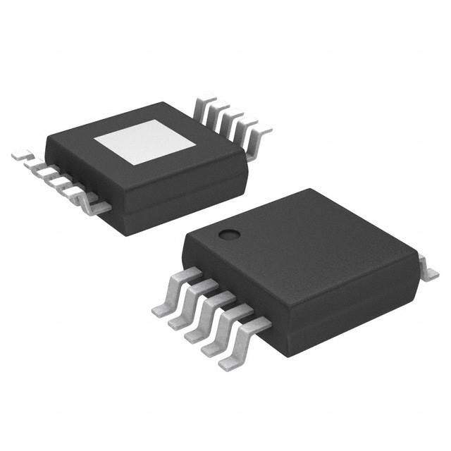
| 产品图片 |
|
| rohs | 符合RoHS无铅 / 符合限制有害物质指令(RoHS)规范要求 |
| 产品系列 | 音频 IC,音频放大器,Texas Instruments TPA0213DGQ- |
| 数据手册 | |
| 产品型号 | TPA0213DGQ |
| THD+噪声 | 0.2 % |
| 不同负载时的最大输出功率x通道数 | 2W x 1 @ 4 欧姆; 90mW x 2 @ 32 欧姆 |
| 产品 | Class-AB |
| 产品种类 | 音频放大器 |
| 供应商器件封装 | 10-MSOP-PowerPad |
| 其它名称 | 296-34548-5 |
| 包装 | 管件 |
| 单位重量 | 18.800 mg |
| 商标 | Texas Instruments |
| 安装类型 | 表面贴装 |
| 安装风格 | SMD/SMT |
| 封装 | Tube |
| 封装/外壳 | 10-TFSOP,10-MSOP(0.118",3.00mm 宽)裸焊盘 |
| 封装/箱体 | HVSSOP-10 |
| 工作温度 | -40°C ~ 85°C (TA) |
| 工作电源电压 | 2.5 V to 5.5 V |
| 工厂包装数量 | 80 |
| 最大功率耗散 | 2140 mW |
| 最大工作温度 | + 85 C |
| 最小工作温度 | - 40 C |
| 标准包装 | 80 |
| 特性 | 消除爆音,输入多路复用器,关机 |
| 电压-电源 | 2.5 V ~ 5.5 V |
| 电源电压-最大 | 5.5 V |
| 电源电压-最小 | 2.5 V |
| 电源电流 | 4.2 mA |
| 电源类型 | Single |
| 类型 | AB 类 |
| 系列 | TPA0213 |
| 输入信号类型 | Single |
| 输出信号类型 | Differential, Single |
| 输出功率 | 2 W |
| 输出类型 | 1-通道(单声道),带立体声耳机 |
| 通道数量 | 1 Channel |
| 配用 | /product-detail/zh/TPA0213EVM/296-10809-ND/381859 |
| 音频负载电阻 | 32 Ohms |


- 商务部:美国ITC正式对集成电路等产品启动337调查
- 曝三星4nm工艺存在良率问题 高通将骁龙8 Gen1或转产台积电
- 太阳诱电将投资9.5亿元在常州建新厂生产MLCC 预计2023年完工
- 英特尔发布欧洲新工厂建设计划 深化IDM 2.0 战略
- 台积电先进制程称霸业界 有大客户加持明年业绩稳了
- 达到5530亿美元!SIA预计今年全球半导体销售额将创下新高
- 英特尔拟将自动驾驶子公司Mobileye上市 估值或超500亿美元
- 三星加码芯片和SET,合并消费电子和移动部门,撤换高东真等 CEO
- 三星电子宣布重大人事变动 还合并消费电子和移动部门
- 海关总署:前11个月进口集成电路产品价值2.52万亿元 增长14.8%


PDF Datasheet 数据手册内容提取
(cid:1)(cid:2)(cid:3)(cid:4)(cid:5)(cid:6)(cid:7) (cid:5)(cid:8)(cid:9) (cid:10)(cid:11)(cid:12)(cid:11) (cid:3)(cid:13)(cid:14)(cid:15)(cid:11) (cid:2)(cid:11)(cid:9)(cid:16)(cid:17) (cid:3)(cid:10)(cid:2)(cid:18)(cid:15)(cid:19)(cid:15)(cid:16)(cid:17) (cid:9)(cid:15)(cid:1)(cid:20) (cid:20)(cid:16)(cid:3)(cid:14)(cid:2)(cid:20)(cid:11)(cid:12)(cid:16) (cid:14)(cid:17)(cid:15)(cid:21)(cid:16) SLOS276D − JANUARY 2000 − REVISED NOVEMBER 2002 (cid:1) Ideal for Notebook Computers, PDAs, and DGQ PACKAGE Other Small Portable Audio Devices (TOP VIEW) (cid:1) 2 W Into 4 Ω From 5-V Supply MONO−IN 1 10 LO/MO− (cid:1) 0.6 W Into 4 Ω From 3-V Supply SHUTDOWN 2 9 LIN (cid:1) Stereo Headphone Drive VDD 3 8 GND (cid:1) BYPASS 4 7 ST/MN Separate Inputs for the Mono (BTL) Signal, RIN 5 6 RO/MO+ and Stereo (SE) Left/Right Signals (cid:1) Wide Power Supply Compatibility 2.5 V to 5.5 V (cid:1) Low Supply Current − 4.2 mA Typical at 5 V − 3.6 mA Typical at 3 V (cid:1) Shutdown Control...1 µA Typical (cid:1) Shutdown Pin Is TTL Compatible (cid:1) −40°C to 85°C Operating Temperature Range (cid:1) Space-Saving, Thermally-Enhanced MSOP Packaging description The TPA0213 is a 2-W mono bridge-tied-load (BTL) amplifier designed to drive speakers with as low as 4-Ω impedance. The amplifier can be reconfigured on the fly to drive two stereo single-ended (SE) signals into headphones. This makes the device ideal for use in small notebook computers, PDAs, personal digital audio players, anywhere a mono speaker and stereo headphones are required. From a 5-V supply, the TPA0213 can deliver 2 W of power into a 4-Ω speaker. The gain of the input stage is set by the user-selected input resistor and a 50-kΩ internal feedback resistor (A = − R /R). The power stage is internally configured with a gain of –1.25 V/V in SE mode, and –2.5 V/V in V F I BTL mode. Thus, the overall gain of the amplifier is −62.5 kΩ/RI in SE mode and −125 kΩ/RI in BTL mode. The TPA0213 is available in the 10-pin thermally-enhanced MSOP package (DGQ) and operates over an ambient temperature range of −40°C to 85°C. AVAILABLE OPTIONS PACKAGED DEVICES MMSSOOPP TA MSOP† SYMBOLIZATION (DGQ) −40°C to 85°C TPA0213DGQ AEH †The DGQ package are available taped and reeled. To order a taped and reeled part, add the suffix R to the part number (e.g., TPA0213DGQR). Please be aware that an important notice concerning availability, standard warranty, and use in critical applications of TexasInstruments semiconductor products and disclaimers thereto appears at the end of this data sheet. (cid:2)(cid:17)(cid:11)(cid:14)(cid:13)(cid:22)(cid:1)(cid:15)(cid:11)(cid:12) (cid:14)(cid:3)(cid:1)(cid:3) (cid:23)(cid:24)(cid:25)(cid:26)(cid:27)(cid:28)(cid:29)(cid:30)(cid:23)(cid:26)(cid:24) (cid:23)(cid:31) !"(cid:27)(cid:27)#(cid:24)(cid:30) (cid:29)(cid:31) (cid:26)(cid:25) $"%&(cid:23)!(cid:29)(cid:30)(cid:23)(cid:26)(cid:24) ’(cid:29)(cid:30)#( Copyright 2002, Texas Instruments Incorporated (cid:2)(cid:27)(cid:26)’"!(cid:30)(cid:31) !(cid:26)(cid:24)(cid:25)(cid:26)(cid:27)(cid:28) (cid:30)(cid:26) (cid:31)$#!(cid:23)(cid:25)(cid:23)!(cid:29)(cid:30)(cid:23)(cid:26)(cid:24)(cid:31) $#(cid:27) (cid:30))# (cid:30)#(cid:27)(cid:28)(cid:31) (cid:26)(cid:25) (cid:1)#*(cid:29)(cid:31) (cid:15)(cid:24)(cid:31)(cid:30)(cid:27)"(cid:28)#(cid:24)(cid:30)(cid:31) (cid:31)(cid:30)(cid:29)(cid:24)’(cid:29)(cid:27)’ +(cid:29)(cid:27)(cid:27)(cid:29)(cid:24)(cid:30),( (cid:2)(cid:27)(cid:26)’"!(cid:30)(cid:23)(cid:26)(cid:24) $(cid:27)(cid:26)!#(cid:31)(cid:31)(cid:23)(cid:24)- ’(cid:26)#(cid:31) (cid:24)(cid:26)(cid:30) (cid:24)#!#(cid:31)(cid:31)(cid:29)(cid:27)(cid:23)&, (cid:23)(cid:24)!&"’# (cid:30)#(cid:31)(cid:30)(cid:23)(cid:24)- (cid:26)(cid:25) (cid:29)&& $(cid:29)(cid:27)(cid:29)(cid:28)#(cid:30)#(cid:27)(cid:31)( POST OFFICE BOX 655303 • DALLAS, TEXAS 75265 1
(cid:1)(cid:2)(cid:3)(cid:4)(cid:5)(cid:6)(cid:7) (cid:5)(cid:8)(cid:9) (cid:10)(cid:11)(cid:12)(cid:11) (cid:3)(cid:13)(cid:14)(cid:15)(cid:11) (cid:2)(cid:11)(cid:9)(cid:16)(cid:17) (cid:3)(cid:10)(cid:2)(cid:18)(cid:15)(cid:19)(cid:15)(cid:16)(cid:17) (cid:9)(cid:15)(cid:1)(cid:20) (cid:20)(cid:16)(cid:3)(cid:14)(cid:2)(cid:20)(cid:11)(cid:12)(cid:16) (cid:14)(cid:17)(cid:15)(cid:21)(cid:16) SLOS276D − JANUARY 2000 − REVISED NOVEMBER 2002 functional block diagram CB 4 BYPASS VDD 3 VDD GND 8 1 kΩ 50 kΩ BYPASS VDD Mono Audio Ci 50 kΩ Input RI 1.25*R 100 kΩ 1 M − R CC Right 5 MONO-IN U − RO/MO+ 6 AInupduito Ci RI RIN X + + BYPASS BYPASS 100 kΩ 50 kΩ Stereo/Mono ST/MN 7 50 kΩ Control 50 kΩ 1.25*R Left Audio Ci M − R CC Input RI 9 LIN U − LO/MO− 10 X + + 1 kΩ BYPASS BYPASS From Shutdown System Control 2 SHUTDOWN and Depop Circuitry 2 POST OFFICE BOX 655303 • DALLAS, TEXAS 75265
(cid:1)(cid:2)(cid:3)(cid:4)(cid:5)(cid:6)(cid:7) (cid:5)(cid:8)(cid:9) (cid:10)(cid:11)(cid:12)(cid:11) (cid:3)(cid:13)(cid:14)(cid:15)(cid:11) (cid:2)(cid:11)(cid:9)(cid:16)(cid:17) (cid:3)(cid:10)(cid:2)(cid:18)(cid:15)(cid:19)(cid:15)(cid:16)(cid:17) (cid:9)(cid:15)(cid:1)(cid:20) (cid:20)(cid:16)(cid:3)(cid:14)(cid:2)(cid:20)(cid:11)(cid:12)(cid:16) (cid:14)(cid:17)(cid:15)(cid:21)(cid:16) SLOS276D − JANUARY 2000 − REVISED NOVEMBER 2002 Terminal Functions TERMINAL II//OO DDEESSCCRRIIPPTTIIOONN NAME NO. BYPASS 4 I BYPASS is the tap to the voltage divider for internal mid-supply bias. This terminal should be connected to a 0.1-µF to 1-µF capacitor. GND 8 Ground terminal LIN 9 I Left-channel input terminal LO/MO− 10 O Left-output in SE mode and mono negative output in BTL mode. MONO-IN 1 I Mono input terminal RIN 5 I Right-channel input terminal RO/MO+ 6 O Right-output in SE mode and mono positive output in BTL mode SHUTDOWN 2 I SHUTDOWN places the entire device in shutdown mode when held low. TTL compatible input. ST/MN 7 I Selects between stereo and mono mode. When held high, the amplifier is in SE stereo mode, while held low, the amplifier is in BTL mono mode. VDD 3 I VDD is the supply voltage terminal. absolute maximum ratings over operating free-air temperature range (unless otherwise noted)§ Supply voltage, V . . . . . . . . . . . . . . . . . . . . . . . . . . . . . . . . . . . . . . . . . . . . . . . . . . . . . . . . . . . . . . . . . . . . . . . . 6 V DD Input voltage range, V . . . . . . . . . . . . . . . . . . . . . . . . . . . . . . . . . . . . . . . . . . . . . . . . . . . . . . . −0.3 V to V +0.3 V I DD Continuous total power dissipation . . . . . . . . . . . . . . . . . . . . . internally limited (see Dissipation Rating Table) Operating free-air temperature range, T (see Table 3) . . . . . . . . . . . . . . . . . . . . . . . . . . . . . . . . −40°C to 85°C A Operating junction temperature range, T . . . . . . . . . . . . . . . . . . . . . . . . . . . . . . . . . . . . . . . . . . . −40°C to 150°C J Storage temperature range, T . . . . . . . . . . . . . . . . . . . . . . . . . . . . . . . . . . . . . . . . . . . . . . . . . . . −65°C to 150°C stg Lead temperature 1,6 mm (1/16 inch) from case for 10 seconds . . . . . . . . . . . . . . . . . . . . . . . . . . . . . . . 260°C §Stresses beyond those listed under “absolute maximum ratings” may cause permanent damage to the device. These are stress ratings only, and functional operation of the device at these or any other conditions beyond those indicated under “recommended operating conditions” is not implied. Exposure to absolute-maximum-rated conditions for extended periods may affect device reliability. DISSIPATION RATING TABLE PACKAGE TA ≤ 25°C DERATING FACTOR TA = 70°C TA = 85°C DGQ 2.14 W¶ 17.1 mW/°C 1.37 W 1.11 W ¶Please see the Texas Instruments document, PowerPAD Thermally Enhanced Package Application Report (SLMA002), for more information on the PowerPAD package. The thermal data was measured on a PCB layout based on the information in the section entitled Texas Instruments Recommended Board for PowerPAD on page 33 of that document. PowerPAD is a trademark of Texas Instruments POST OFFICE BOX 655303 • DALLAS, TEXAS 75265 3
(cid:1)(cid:2)(cid:3)(cid:4)(cid:5)(cid:6)(cid:7) (cid:5)(cid:8)(cid:9) (cid:10)(cid:11)(cid:12)(cid:11) (cid:3)(cid:13)(cid:14)(cid:15)(cid:11) (cid:2)(cid:11)(cid:9)(cid:16)(cid:17) (cid:3)(cid:10)(cid:2)(cid:18)(cid:15)(cid:19)(cid:15)(cid:16)(cid:17) (cid:9)(cid:15)(cid:1)(cid:20) (cid:20)(cid:16)(cid:3)(cid:14)(cid:2)(cid:20)(cid:11)(cid:12)(cid:16) (cid:14)(cid:17)(cid:15)(cid:21)(cid:16) SLOS276D − JANUARY 2000 − REVISED NOVEMBER 2002 recommended operating conditions ÁÁÁÁÁÁÁÁÁÁÁÁÁÁÁÁÁÁÁÁÁÁÁÁÁÁÁÁÁÁÁÁÁÁÁÁÁ MIN MAX UNIT ÁÁSupÁply vÁoltaÁge, VÁDDÁÁÁÁÁÁÁÁÁÁÁÁÁÁÁÁÁÁÁÁÁÁÁÁ2.5ÁÁÁ5.5ÁÁÁV Á VDD = 3 V 2.7 SSTT//MMNN HHiigghh--lleevveell iinnppuutt vvoollttaaggee,, VVIIHH VDD = 5 V 4.5 VV SHUTDOWN 2 VDD = 3 V 1.65 SSTT//MMNN LLooww--lleevveell iinnppuutt vvoollttaaggee,, VVIILL VDD = 5 V 2.75 VV SHUTDOWN 0.8 ÁÁOpeÁratinÁg freÁe-aiÁr temÁperÁatureÁ, TAÁÁÁÁÁÁÁÁÁÁÁÁÁÁÁÁÁÁÁÁÁ−40ÁÁÁ85ÁÁÁ°C Á ÁÁÁÁÁÁÁÁÁÁÁÁÁÁÁÁÁÁÁÁÁÁÁÁÁÁÁÁÁÁÁÁÁÁÁÁÁ electrical characteristics at specified free-air temperature, V = 3 V, T = 25°C (unless otherwise DD A noted) ÁÁÁÁÁÁÁÁPARÁAMÁETEÁR ÁÁÁÁÁÁÁÁÁTÁESTÁ COÁNDITÁIONÁS ÁÁÁÁÁMINÁÁÁTYPÁÁMÁAXÁÁUÁNITÁ ÁÁÁÁ|VOÁÁO| ÁÁÁÁOÁÁutpÁÁut ofÁÁfset ÁÁvoltaÁÁge (mÁÁeaÁÁsureÁÁd diffÁÁerenÁÁtiallyÁÁÁÁ) ÁÁRL =ÁÁ 4 ΩÁÁ, STÁÁ/MNÁÁ = 0 ÁÁV, SÁÁHUTÁÁÁDOWÁÁN =ÁÁ 2 VÁÁÁÁÁÁÁÁÁÁÁÁÁÁÁÁÁÁ30ÁÁÁÁÁÁmV ÁÁ ÁÁPSRÁR ÁÁPÁoweÁr suÁpplyÁ rejeÁctionÁ ratioÁÁÁÁÁÁÁVDDÁ = 2Á.9 VÁ to 3Á.1 V,ÁÁÁÁBTÁL mÁodeÁÁÁÁÁÁÁÁÁÁÁ65ÁÁÁÁÁÁÁÁÁÁÁÁdB ÁÁ SHUTDOWN, VDD = 3.3 V, VI = VDD 1 ||IIIIHH|| HHiigghh--lleevveell iinnppuutt ccuurrrreenntt ÁÁÁÁÁÁÁÁÁÁÁÁÁÁÁÁÁÁÁÁÁÁµAA ÁÁ ST/MN, VDD = 3.3 V, VI = VDD 1 ÁÁÁÁÁÁÁÁÁÁÁÁÁÁÁÁÁÁÁÁÁÁÁÁÁÁÁÁÁÁÁÁÁÁÁÁ SHUTDOWN, VDD = 3.3 V, VI = 0 V 1 ||IIIILL|| LLooww--lleevveell iinnppuutt ccuurrrreenntt ÁÁÁÁÁÁÁÁÁÁÁÁÁÁÁÁÁÁÁÁÁÁµAA ÁÁ ST/MN, VDD = 3.3 V, VI = 0 V 1 ÁÁzi ÁÁÁIÁnputÁ impÁedanÁce ÁÁÁÁÁÁÁÁÁÁÁÁÁÁÁÁÁÁÁÁÁÁÁÁÁÁÁÁÁ50ÁÁÁÁÁÁÁÁÁÁÁÁkΩ ÁÁ ÁÁÁÁIDDÁÁÁÁÁÁSÁÁuppÁÁly cuÁÁrrenÁÁt ÁÁÁÁÁÁÁÁÁÁÁÁÁÁÁÁÁÁVDDÁÁ = 2ÁÁ.5 V,ÁÁ SHÁÁUTDÁÁOWNÁÁ = 2ÁÁ V ÁÁÁÁÁÁÁÁÁÁÁÁÁÁÁÁ3.6ÁÁÁÁÁÁ5.5ÁÁÁÁÁÁmA ÁÁ ÁÁÁÁIDDÁÁ(SD)ÁÁÁÁSÁÁuppÁÁly cuÁÁrrenÁÁt, shÁÁutdoÁÁwn mÁÁodeÁÁÁÁÁÁÁÁÁÁÁÁSHUÁÁTDOÁÁWNÁÁ = 0ÁÁ V ÁÁÁÁÁÁÁÁÁÁÁÁÁÁÁÁÁÁÁÁÁÁ1ÁÁÁÁÁÁ10ÁÁÁÁÁÁµA ÁÁ ÁÁRFÁÁÁFÁeedÁbackÁ resÁistorÁÁÁÁÁÁÁÁÁVDDÁ = 2Á.5 V,Á RL Á= 4 ΩÁ, STÁ/MNÁ = 1Á.375Á V, ÁÁÁ46ÁÁÁ50ÁÁÁ57ÁÁÁkΩ Á SHUTDOWN = 2 V ÁÁÁÁÁÁÁÁÁÁÁÁÁÁÁÁÁÁÁÁÁÁÁÁÁÁÁÁÁÁÁÁÁÁÁÁÁÁÁÁ operating characteristics, VDD = 3 V, TA = 25°C, RL = 4 Ω, f = 1 kHz (unless otherwise noted) PARAMETER TEST CONDITIONS MIN TYP MAX UNIT ÁÁÁÁÁÁÁÁÁÁÁÁÁÁÁÁÁÁÁÁÁÁÁÁÁÁÁÁÁÁÁÁÁÁÁÁÁÁÁÁÁÁÁÁÁÁÁÁÁÁÁÁÁÁÁÁÁÁÁÁÁÁÁÁÁÁÁÁÁÁÁÁÁÁÁÁÁÁÁÁÁÁÁÁ THD = 1%, BTL mode 660 ÁÁÁÁPPOOÁÁÁÁÁÁOOÁÁuuttppÁÁuutt ppooÁÁwweerr,,ÁÁ sseeeeÁÁ NNoottÁÁee 11 ÁÁÁÁÁÁÁÁTHÁÁD =ÁÁ 0.1ÁÁ%, ÁÁÁÁSEÁÁ moÁÁde,ÁÁÁÁÁÁÁÁRÁÁL = ÁÁ32 ΩÁÁÁÁÁÁÁÁÁÁÁÁÁÁ33ÁÁÁÁÁÁÁÁÁÁmmÁÁWWÁÁ ÁÁÁÁTHDÁÁ + NÁÁÁÁTÁÁotal ÁÁharmÁÁoniÁÁc disÁÁtortioÁÁn plÁÁus nÁÁoiseÁÁÁÁPOÁÁ = 5ÁÁ00 mÁÁW,ÁÁÁÁf =ÁÁ 20 ÁÁHz toÁÁ 20ÁÁ kHzÁÁÁÁÁÁÁÁÁÁÁÁÁÁÁÁÁÁÁÁ0ÁÁ.2%ÁÁÁÁÁÁÁÁÁÁÁÁÁÁ ÁÁÁÁBOMÁÁÁÁÁÁMÁÁaximÁÁumÁÁ outÁÁput pÁÁoweÁÁr baÁÁndwiÁÁdth ÁÁÁÁGÁÁain =ÁÁ 8 dÁÁB, ÁÁÁÁTHÁÁD =ÁÁ 2%ÁÁÁÁÁÁÁÁÁÁÁÁÁÁÁÁÁÁÁÁÁÁÁÁÁÁ20ÁÁÁÁÁÁÁÁÁÁkÁÁHz ÁÁ ÁÁÁÁÁÁÁÁÁÁÁÁÁÁÁÁÁÁÁÁÁÁÁÁÁÁÁÁÁÁÁÁÁÁÁÁÁÁÁÁÁÁÁÁÁÁÁÁÁÁÁÁBÁÁTL mÁÁodeÁÁÁÁÁÁÁÁÁÁÁÁÁÁ52ÁÁÁÁÁÁÁÁÁÁÁÁÁÁ SSuuppppllyy rriippppllee rreejjeeccttiioonn rraattiioo ff == 11 kkHHzz,, CCBB == 00..4477 µFF ddBB SE mode 62 ÁÁÁÁÁÁÁÁÁÁÁÁÁÁÁÁÁÁÁÁÁÁÁÁÁÁÁÁÁÁÁÁÁÁÁÁÁÁÁÁÁÁÁÁÁÁÁÁÁÁÁÁÁÁÁÁÁÁÁÁÁÁÁÁÁÁÁÁÁÁÁÁÁÁÁÁÁÁÁÁÁÁÁÁ BTL mode 42 ÁÁÁÁVVnnÁÁÁÁÁÁNNÁÁooiisseeÁÁ oouuttÁÁppuutt vvÁÁoollttaaÁÁggee ÁÁÁÁÁÁÁÁÁÁCCÁÁBB == 00ÁÁ..4477 ÁÁµµFF,,ÁÁÁÁff ==ÁÁ 2200 ÁÁHHzz ttooÁÁ 2200ÁÁ kkHHzzÁÁÁÁÁÁÁÁÁÁÁÁÁÁÁÁÁÁÁÁÁÁÁÁÁÁÁÁÁÁÁÁµµVVÁÁRRMMSSÁÁ SE mode 21 ÁÁÁÁÁÁÁÁÁÁÁÁÁÁÁÁÁÁÁÁÁÁÁÁÁÁÁÁÁÁÁÁÁÁÁÁÁÁÁÁÁÁ NOTE 1: Output power is measured at the output terminals of the device at f = 1 kHz. 4 POST OFFICE BOX 655303 • DALLAS, TEXAS 75265
(cid:1)(cid:2)(cid:3)(cid:4)(cid:5)(cid:6)(cid:7) (cid:5)(cid:8)(cid:9) (cid:10)(cid:11)(cid:12)(cid:11) (cid:3)(cid:13)(cid:14)(cid:15)(cid:11) (cid:2)(cid:11)(cid:9)(cid:16)(cid:17) (cid:3)(cid:10)(cid:2)(cid:18)(cid:15)(cid:19)(cid:15)(cid:16)(cid:17) (cid:9)(cid:15)(cid:1)(cid:20) (cid:20)(cid:16)(cid:3)(cid:14)(cid:2)(cid:20)(cid:11)(cid:12)(cid:16) (cid:14)(cid:17)(cid:15)(cid:21)(cid:16) SLOS276D − JANUARY 2000 − REVISED NOVEMBER 2002 electrical characteristics at specified free-air temperature, V = 5 V, T = 25°C (unless otherwise DD A noted) ÁÁÁÁÁÁÁPAÁRAÁMETÁERÁÁÁÁÁÁÁÁÁÁTESÁT COÁNDÁITIOÁNSÁÁÁÁÁMIÁÁN ÁTYÁÁP ÁMAXÁÁÁUNIÁT ÁÁ|VÁÁOO|ÁÁÁÁÁÁOutÁÁput oÁÁffseÁÁt volÁÁtageÁÁ (meÁÁasurÁÁed dÁÁiffereÁÁntiaÁÁlly) ÁÁÁÁRLÁÁ = 4ÁÁ Ω, SÁÁT/MÁÁN = ÁÁ0 V, ÁÁSHUÁÁÁTDOÁÁWNÁÁ = 2ÁÁÁÁ V ÁÁÁÁÁÁÁÁÁÁÁÁÁÁ3ÁÁÁÁ0 ÁÁmVÁÁ ÁPSÁRRÁÁÁPowÁer sÁupplÁy rejÁectioÁn raÁtio ÁÁÁÁÁÁVDÁD =Á 4.9 ÁV to Á5.1 VÁ, ÁÁÁBÁTL mÁodeÁÁÁÁÁÁÁÁÁÁÁ6ÁÁÁÁ2 ÁÁÁÁÁÁÁÁdBÁÁ SHUTDOWN, VDD = 5.5 V, VI = VDD 1 ||IIIIHH|| HHiigghh--lleevveell iinnppuutt ccuurrrreenntt ÁÁÁÁÁÁÁÁÁÁÁÁÁÁÁÁÁÁÁÁÁÁµAAÁÁ ST/MN, VDD = 5.5 V, VI = VDD 1 ÁÁÁÁÁÁÁÁÁÁÁÁÁÁÁÁÁÁÁÁÁÁÁÁ SHUTDOWN, VDD = 5.5 V, VI = 0 V 1 ||IIIILL|| LLooww--lleevveell iinnppuutt ccuurrrreenntt ÁÁÁÁÁÁÁÁÁÁÁÁÁÁÁÁÁÁÁÁÁÁÁÁÁÁÁÁÁÁÁÁÁµAAÁÁÁ ST/MN, VDD = 5.5 V, VI = 0 V 1 ÁziÁÁÁÁInpuÁt imÁpedaÁnceÁÁÁÁÁÁÁÁÁÁÁÁÁÁÁÁÁÁÁÁÁÁÁÁÁÁÁÁÁ5ÁÁÁÁ0 ÁÁÁÁÁÁÁÁkΩÁÁ ÁÁIDÁÁD ÁÁÁÁÁÁSupÁÁply cÁÁurreÁÁnt ÁÁÁÁÁÁÁÁÁÁÁÁÁÁÁÁÁÁSHÁÁUTDÁÁOWÁÁN =ÁÁ 2 VÁÁÁÁÁÁÁÁÁÁÁÁÁÁÁÁÁÁÁÁÁÁ4.ÁÁÁÁ2 ÁÁ6.ÁÁÁÁ3 ÁÁmAÁÁ ÁIDÁD(SDÁ) ÁÁSupÁply cÁurreÁnt, sÁhutdÁownÁ modÁe ÁÁÁÁÁSHÁUTDÁOWÁN =Á 0 VÁÁÁÁÁÁÁÁÁÁÁÁÁ1 Á1ÁÁ0 ÁµAÁ operating characteristics, VDD = 5 V, TA = 25°C, RL = 4 Ω ÁÁÁÁÁÁPARÁAMÁETEÁR ÁÁÁÁÁÁÁÁÁÁTEÁST ÁCONÁDITÁIONÁÁS ÁÁÁÁÁÁMINÁÁÁTYPÁÁMÁAXÁÁÁUNITÁ THD = 0.3%, BTL mode 2 W ÁÁÁÁÁÁÁÁÁÁÁÁÁÁÁÁÁÁÁÁÁÁÁÁÁÁÁÁÁÁÁÁÁÁÁÁÁÁÁÁÁÁÁÁÁÁÁÁÁÁÁÁÁÁÁÁÁÁÁÁÁÁÁÁÁÁÁÁÁÁÁÁÁÁÁÁÁÁÁÁÁÁ PPOO OOuuttppuutt ppoowweerr,, sseeee NNoottee 11 THD = 0.1%, SE mode, RL = 32 Ω 90 mW ÁÁÁÁÁÁÁÁÁÁÁÁÁÁÁÁÁÁÁÁÁÁÁÁÁÁÁÁÁÁÁÁÁÁÁÁÁÁÁÁÁÁÁÁÁÁÁÁÁÁÁÁÁÁÁÁÁÁÁÁÁÁÁÁÁÁÁÁÁÁÁÁÁÁÁÁÁÁÁÁÁÁ Total harmonic distortion plus ÁÁTHÁÁD +ÁÁ N ÁÁÁÁnoisÁÁe ÁÁÁÁÁÁÁÁÁÁÁÁÁÁÁÁPÁÁO =ÁÁ 1.5 ÁÁW, ÁÁÁÁf ÁÁ= 20ÁÁ Hz ÁÁto 20ÁÁ kHzÁÁÁÁÁÁÁÁÁÁÁÁÁÁÁÁÁÁÁÁÁÁ0.2%ÁÁÁÁÁÁÁÁÁÁÁÁÁÁ ÁÁBOÁÁM ÁÁÁÁÁÁMaxÁÁimuÁÁm ouÁÁtputÁÁ powÁÁer bÁÁandwÁÁidthÁÁÁÁGÁÁain ÁÁ= 6 dÁÁB, ÁÁÁÁTÁÁHD =ÁÁ 2%ÁÁÁÁÁÁÁÁÁÁÁÁÁÁÁÁÁÁÁÁÁÁÁÁÁÁ20ÁÁÁÁÁÁÁÁÁÁÁÁkHzÁÁ ÁÁÁÁÁÁÁÁÁÁÁÁÁÁÁÁÁÁÁÁÁÁÁÁÁÁÁÁÁÁÁÁÁÁÁÁÁÁÁÁÁÁÁÁÁÁÁÁÁÁBÁÁTL ÁÁmodÁÁe ÁÁÁÁÁÁÁÁÁÁÁÁ52ÁÁÁÁÁÁÁÁÁÁÁÁÁÁ SSuuppppllyy rriippppllee rreejjeeccttiioonn rraattiioo ff == 11 kkHHzz,, CCBB == 00..4477 µFF ddBB SE mode 62 ÁÁÁÁÁÁÁÁÁÁÁÁÁÁÁÁÁÁÁÁÁÁÁÁÁÁÁÁÁÁÁÁÁÁÁÁÁÁÁÁÁÁÁÁÁÁÁÁÁÁÁÁÁÁÁÁÁÁÁÁÁÁÁÁÁÁÁÁÁÁÁÁÁÁÁÁÁÁÁÁÁÁ BTL mode 42 ÁÁVVnnÁÁÁÁÁÁÁÁNNooiiÁÁssee ooÁÁuuttppuuÁÁtt vvoollttÁÁaaggeeÁÁÁÁÁÁÁÁÁÁCCÁÁBB == ÁÁ00..4477ÁÁ µFF,,ÁÁÁÁff ÁÁ== 2200ÁÁ HHzz ÁÁttoo 2200ÁÁ kkHHzzÁÁÁÁÁÁÁÁÁÁÁÁÁÁÁÁÁÁÁÁÁÁÁÁÁÁÁÁÁÁÁÁµÁÁVVRRMMÁÁSS SE mode 21 ÁÁÁÁÁÁÁÁÁÁÁÁÁÁÁÁÁÁÁÁÁÁÁÁÁÁÁÁÁÁÁÁÁÁÁÁÁÁÁÁÁ NOTE 1: Output power is measured at the output terminals of the device at f = 1 kHz. TYPICAL CHARACTERISTICS Table of Graphs FIGURE vs Output power 1, 3, 5, 6, 8, 10 TTHHDD++NN TToottaall hhaarrmmoonniicc ddiissttoorrttiioonn pplluuss nnooiissee vs Frequency 2, 4, 7, 9 Vn Output noise voltage vs Frequency 11 Power supply rejection ratio vs Frequency 12, 13 POST OFFICE BOX 655303 • DALLAS, TEXAS 75265 5
(cid:1)(cid:2)(cid:3)(cid:4)(cid:5)(cid:6)(cid:7) (cid:5)(cid:8)(cid:9) (cid:10)(cid:11)(cid:12)(cid:11) (cid:3)(cid:13)(cid:14)(cid:15)(cid:11) (cid:2)(cid:11)(cid:9)(cid:16)(cid:17) (cid:3)(cid:10)(cid:2)(cid:18)(cid:15)(cid:19)(cid:15)(cid:16)(cid:17) (cid:9)(cid:15)(cid:1)(cid:20) (cid:20)(cid:16)(cid:3)(cid:14)(cid:2)(cid:20)(cid:11)(cid:12)(cid:16) (cid:14)(cid:17)(cid:15)(cid:21)(cid:16) SLOS276D − JANUARY 2000 − REVISED NOVEMBER 2002 TYPICAL CHARACTERISTICS TOTAL HARMONIC DISTORTION + NOISE TOTAL HARMONIC DISTORTION + NOISE vs vs OUTPUT POWER FREQUENCY 10 1 Distortion + Noise 1 VMfG =Dao iDn1n o k==/HB3 8 zTV dLB Distortion + Noise 0.1 VMRPODLo Dn ==o =82/B 53ΩT0 V LmWGain = 20 dB monic RL = 4 Ω monic Har Har Gain = 8 dB N − Total .10 RL = 8 Ω N − Total 0.01 D+ D+ H H T T .01 0.001 0.001 0.01 0.1 1 10 10 100 1k 10k 20k PO − Output Power − W f − Frequency − Hz Figure 1 Figure 2 TOTAL HARMONIC DISTORTION + NOISE TOTAL HARMONIC DISTORTION + NOISE vs vs OUTPUT POWER FREQUENCY 10 1 VDD = 3 V VDD = 3 V Distortion + Noise 1 GMRf La=oi nn=2o 0 8=/ B k Ω8HT dLzB Distortion + Noise 0.1 SGtaeirne =o /1S.E9 dB PROL = = 2 352 m ΩW monic monic Har Har D+N − Total 0.1 f = 20 Hz f = 1 kHz D+N − Total 0.01 VROL = = 1 1 V0R kMΩS H H T T 0.01 0.001 0.001 0.01 0.1 1 2 10 100 1k 10k 20k PO − Output Power − W f − Frequency − Hz Figure 3 Figure 4 6 POST OFFICE BOX 655303 • DALLAS, TEXAS 75265
(cid:1)(cid:2)(cid:3)(cid:4)(cid:5)(cid:6)(cid:7) (cid:5)(cid:8)(cid:9) (cid:10)(cid:11)(cid:12)(cid:11) (cid:3)(cid:13)(cid:14)(cid:15)(cid:11) (cid:2)(cid:11)(cid:9)(cid:16)(cid:17) (cid:3)(cid:10)(cid:2)(cid:18)(cid:15)(cid:19)(cid:15)(cid:16)(cid:17) (cid:9)(cid:15)(cid:1)(cid:20) (cid:20)(cid:16)(cid:3)(cid:14)(cid:2)(cid:20)(cid:11)(cid:12)(cid:16) (cid:14)(cid:17)(cid:15)(cid:21)(cid:16) SLOS276D − JANUARY 2000 − REVISED NOVEMBER 2002 TYPICAL CHARACTERISTICS TOTAL HARMONIC DISTORTION + NOISE TOTAL HARMONIC DISTORTION + NOISE vs vs OUTPUT POWER OUTPUT POWER 10 10 VDD = 3 V VDD = 5 V Noise SRtLe r=e 3o2/S ΩE Noise Mf =o n1 ok/HBzTL Distortion + 1 Gain = 1.9 dB Distortion + 1 Gain = 8 dB monic f = 20 kHz monic RL = 4 Ω Har Har N − Total 0.1 f = 1 kHz N − Total 0.1 RL = 8 Ω D+ D+ H H T f = 20 Hz T 0.01 0.01 0.01 0.1 0.001 0.01 0.1 1 10 PO − Output Power − W PO − Output Power − W Figure 5 Figure 6 TOTAL HARMONIC DISTORTION + NOISE TOTAL HARMONIC DISTORTION + NOISE vs vs FREQUENCY OUTPUT POWER 1 10 VDD = 5 V VDD = 5 V Noise MRLo n=o 8/B ΩTL Noise MRLo n=o 8/B ΩTL Distortion + 0.1 PO = 1 W Gain = 20 dB Distortion + 1 Gain = 8 dB f = 20 kHz monic monic Har Gain = 8 dB Har f = 1 kHz N − Total 0.01 N − Total 0.1 f = 20 Hz D+ D+ H H T T 0.001 0.01 10 100 1k 10k 20k 0.001 0.01 0.1 1 2 f − Frequency − Hz PO − Output Power − W Figure 7 Figure 8 POST OFFICE BOX 655303 • DALLAS, TEXAS 75265 7
(cid:1)(cid:2)(cid:3)(cid:4)(cid:5)(cid:6)(cid:7) (cid:5)(cid:8)(cid:9) (cid:10)(cid:11)(cid:12)(cid:11) (cid:3)(cid:13)(cid:14)(cid:15)(cid:11) (cid:2)(cid:11)(cid:9)(cid:16)(cid:17) (cid:3)(cid:10)(cid:2)(cid:18)(cid:15)(cid:19)(cid:15)(cid:16)(cid:17) (cid:9)(cid:15)(cid:1)(cid:20) (cid:20)(cid:16)(cid:3)(cid:14)(cid:2)(cid:20)(cid:11)(cid:12)(cid:16) (cid:14)(cid:17)(cid:15)(cid:21)(cid:16) SLOS276D − JANUARY 2000 − REVISED NOVEMBER 2002 TYPICAL CHARACTERISTICS TOTAL HARMONIC DISTORTION + NOISE TOTAL HARMONIC DISTORTION + NOISE vs vs FREQUENCY OUTPUT POWER 1 10 VDD = 5 V VDD = 5 V Noise SGtaeirne =o /1S.E9 dB Noise SRtLe r=e 3o2/S ΩE Distortion + 0.1 Distortion + 1 Gain = 1.9 dB monic PROL = = 7 352 m ΩW monic Har Har f = 20 kHz N − Total 0.01 VROL = = 1 1 V0R kMΩS N − Total 0.1 f = 1 kHz D+ D+ H H T T f = 20 Hz 0.001 0.01 10 100 1k 10k 20k 0.01 0.1 1 f − Frequency − Hz PO − Output Power − W Figure 9 Figure 10 OUTPUT NOISE VOLTAGE POWER SUPPLY REJECTION RATIO vs vs FREQUENCY FREQUENCY 100 0 VDD = 5 V B V Mono/BTL Mono/BTL − d −20 CB = 0.47 µF MGaoinno =/B 8T dLB µe − RGLai n= 8= Ω20 dB GRLai n= 8= Ω8 dB Ratio CB = 1 µF Voltag ction −40 CB = 10 µF se eje Noi Stereo/SE Stereo/SE y R −60 ut RL = 32 Ω RL = 32 Ω ppl p Gain = 14 dB Gain = 1.9 dB u ut S − O wer −80 Bypass = 2.5 V Vn Po − R −100 R S P 10 −120 10 100 1k 10k 20k 20 100 1k 10k 20k f − Frequency − Hz f − Frequency − Hz Figure 11 Figure 12 8 POST OFFICE BOX 655303 • DALLAS, TEXAS 75265
(cid:1)(cid:2)(cid:3)(cid:4)(cid:5)(cid:6)(cid:7) (cid:5)(cid:8)(cid:9) (cid:10)(cid:11)(cid:12)(cid:11) (cid:3)(cid:13)(cid:14)(cid:15)(cid:11) (cid:2)(cid:11)(cid:9)(cid:16)(cid:17) (cid:3)(cid:10)(cid:2)(cid:18)(cid:15)(cid:19)(cid:15)(cid:16)(cid:17) (cid:9)(cid:15)(cid:1)(cid:20) (cid:20)(cid:16)(cid:3)(cid:14)(cid:2)(cid:20)(cid:11)(cid:12)(cid:16) (cid:14)(cid:17)(cid:15)(cid:21)(cid:16) SLOS276D − JANUARY 2000 − REVISED NOVEMBER 2002 TYPICAL CHARACTERISTICS POWER SUPPLY REJECTION RATIO vs FREQUENCY 0 VDD = 5 V B Stereo/SE d − −20 Gain = 1.9 dB o ati CB = 0.47 µF R n ctio −40 CB = 1 µF e ej R y −60 pl p u S er −80 Bypass = 2.5 V w o P − R −100 R S P −120 20 100 1k 10k 20k f − Frequency − Hz Figure 13 APPLICATION INFORMATION gain setting via input resistance The gain of the input stage is set by the user-selected input resistor and a 50-kΩ internal feedback resistor. However, the power stage is internally configured with a gain of −1.25 V/V in SE mode, and −2.5 V/V in BTL mode. Thus, the feedback resistor (R ) is effectively 62.5 kΩ in SE mode and 125 kΩ in BTL mode. Therefore, F the overall gain can be calculated using equations (1) and (2). A (cid:1)–125k(cid:1) (BTL) V R (1) I A (cid:1)–62.5k(cid:1) (SE) V R (2) I The −3 dB frequency can be calculated using equation 3: ƒ (cid:1) 1 (3) –3dB 2(cid:2)R C I i If the filter must be more accurate, the value of the capacitor should be increased while the value of the resistor to ground should be decreased. In addition, the order of the filter could be increased. POST OFFICE BOX 655303 • DALLAS, TEXAS 75265 9
(cid:1)(cid:2)(cid:3)(cid:4)(cid:5)(cid:6)(cid:7) (cid:5)(cid:8)(cid:9) (cid:10)(cid:11)(cid:12)(cid:11) (cid:3)(cid:13)(cid:14)(cid:15)(cid:11) (cid:2)(cid:11)(cid:9)(cid:16)(cid:17) (cid:3)(cid:10)(cid:2)(cid:18)(cid:15)(cid:19)(cid:15)(cid:16)(cid:17) (cid:9)(cid:15)(cid:1)(cid:20) (cid:20)(cid:16)(cid:3)(cid:14)(cid:2)(cid:20)(cid:11)(cid:12)(cid:16) (cid:14)(cid:17)(cid:15)(cid:21)(cid:16) SLOS276D − JANUARY 2000 − REVISED NOVEMBER 2002 APPLICATION INFORMATION input capacitor, C i In the typical application an input capacitor, C, is required to allow the amplifier to bias the input signal to the i proper dc level for optimum operation. In this case, C and the input resistance of the amplifier, R, form a i I high-pass filter with the corner frequency determined in equation 4. −3 dB f (cid:1) 1 (4) c(highpass) 2(cid:2)R C I i fc The value of C is important to consider as it directly affects the bass (low frequency) performance of the circuit. i Consider the example where R is 710 kΩ and the specification calls for a flat bass response down to 40 Hz. I Equation 2 is reconfigured as equation 5. C (cid:1) 1 i 2(cid:2)RIfc (5) In this example, C is 5.6 nF so one would likely choose a value in the range of 5.6 nF to 1 µF. A further I consideration for this capacitor is the leakage path from the input source through the input network (C) and the i feedback network to the load. This leakage current creates a dc offset voltage at the input to the amplifier that reduces useful headroom, especially in high gain applications. For this reason a low-leakage tantalum or ceramic capacitor is the best choice. When polarized capacitors are used, the positive side of the capacitor should face the amplifier input in most applications as the dc level there is held at V /2, which is likely higher DD than the source dc level. Note that it is important to confirm the capacitor polarity in the application. power supply decoupling, C (S) The TPA0213 is a high-performance CMOS audio amplifier that requires adequate power supply decoupling to ensure the output total harmonic distortion (THD) is as low as possible. Power supply decoupling also prevents oscillations for long lead lengths between the amplifier and the speaker. The optimum decoupling is achieved by using two capacitors of different types that target different types of noise on the power supply leads. For higher frequency transients, spikes, or digital hash on the line, a good low equivalent-series-resistance (ESR) ceramic capacitor, typically 0.1 µF placed as close as possible to the device V lead, works best. For DD filtering lower-frequency noise signals, a larger aluminum electrolytic capacitor of 10 µF or greater placed near the audio power amplifier is recommended. midrail bypass capacitor, C (BYP) The midrail bypass capacitor, C , is the most critical capacitor and serves several important functions. (BYP) During start-up or recovery from shutdown mode, C determines the rate at which the amplifier starts up. (BYP) The second function is to reduce noise produced by the power supply caused by coupling into the output drive signal. This noise is from the midrail generation circuit internal to the amplifier, which appears as degraded PSRR and THD+N. Bypass capacitor, C , values of 0.47 µF to 1 µF ceramic or tantalum low-ESR capacitors are recommended (BYP) for the best THD and noise performance. 10 POST OFFICE BOX 655303 • DALLAS, TEXAS 75265
(cid:1)(cid:2)(cid:3)(cid:4)(cid:5)(cid:6)(cid:7) (cid:5)(cid:8)(cid:9) (cid:10)(cid:11)(cid:12)(cid:11) (cid:3)(cid:13)(cid:14)(cid:15)(cid:11) (cid:2)(cid:11)(cid:9)(cid:16)(cid:17) (cid:3)(cid:10)(cid:2)(cid:18)(cid:15)(cid:19)(cid:15)(cid:16)(cid:17) (cid:9)(cid:15)(cid:1)(cid:20) (cid:20)(cid:16)(cid:3)(cid:14)(cid:2)(cid:20)(cid:11)(cid:12)(cid:16) (cid:14)(cid:17)(cid:15)(cid:21)(cid:16) SLOS276D − JANUARY 2000 − REVISED NOVEMBER 2002 APPLICATION INFORMATION output coupling capacitor, C (C) In the typical single-supply SE configuration, an output coupling capacitor (C ) is required to block the dc bias (C) at the output of the amplifier, thus preventing dc currents in the load. As with the input coupling capacitor, the output coupling capacitor and impedance of the load form a high-pass filter governed by equation 6. −3 dB fc(high) (cid:1) 2(cid:2)R1C (6) L (C) fc The main disadvantage, from a performance standpoint, is that the load impedances are typically small, which drives the low-frequency corner higher, degrading the bass response. Large values of C are required to pass (C) low frequencies into the load. Consider the example where a C of 330 µF is chosen and loads vary from (C) 3 Ω, 4 Ω, 8 Ω, 32 Ω, 10 kΩ, to 47 kΩ. Table 1 summarizes the frequency response characteristics of each configuration. Table 1. Common Load Impedances vs Low Frequency Output Characteristics in SE Mode RL C(C) Lowest Frequency 3 Ω 330 µF 161 Hz 4 Ω 330 µF 120 Hz 8 Ω 330 µF 60 Hz 32 Ω 330 µF (cid:1)15 Hz 10,000 Ω 330 µF 0.05 Hz 47,000 Ω 330 µF 0.01 Hz As Table 1 indicates, most of the bass response is attenuated into a 4-Ω load, an 8-Ω load is adequate, headphone response is good, and drive into line level inputs (a home stereo for example) is exceptional. Furthermore, the total amount of ripple current that must flow through the capacitor must be considered when choosing the component. As shown in the application circuit, one coupling capacitor must be in series with the mono loudspeaker for proper operation of the stereo-mono switching circuit. For a 4-Ω load, this capacitor must be able to handle about 700 mA of ripple current for a continuous output power of 2 W. using low-ESR capacitors Low-ESR capacitors are recommended throughout this applications section. A real (as opposed to ideal) capacitor can be modeled simply as a resistor in series with an ideal capacitor. The voltage drop across this resistor minimizes the beneficial effects of the capacitor in the circuit. The lower the equivalent value of this resistance the more the real capacitor behaves like an ideal capacitor. POST OFFICE BOX 655303 • DALLAS, TEXAS 75265 11
(cid:1)(cid:2)(cid:3)(cid:4)(cid:5)(cid:6)(cid:7) (cid:5)(cid:8)(cid:9) (cid:10)(cid:11)(cid:12)(cid:11) (cid:3)(cid:13)(cid:14)(cid:15)(cid:11) (cid:2)(cid:11)(cid:9)(cid:16)(cid:17) (cid:3)(cid:10)(cid:2)(cid:18)(cid:15)(cid:19)(cid:15)(cid:16)(cid:17) (cid:9)(cid:15)(cid:1)(cid:20) (cid:20)(cid:16)(cid:3)(cid:14)(cid:2)(cid:20)(cid:11)(cid:12)(cid:16) (cid:14)(cid:17)(cid:15)(cid:21)(cid:16) SLOS276D − JANUARY 2000 − REVISED NOVEMBER 2002 APPLICATION INFORMATION bridged-tied load versus single-ended mode Figure 14 shows a Class-AB audio power amplifier (APA) in a BTL configuration. The TPA0213 BTL amplifier consists of two Class-AB amplifiers driving both ends of the load. There are several potential benefits to this differential drive configuration, but initially consider power to the load. The differential drive to the speaker means that as one side is slewing up, the other side is slewing down, and vice versa. This, in effect, doubles the voltage swing on the load as compared to a ground referenced load. Plugging 2 × V into the power O(PP) equation, where voltage is squared, yields 4× the output power from the same supply rail and load impedance. See equation 7. V V (cid:1) O(PP) (7) (RMS) 2(cid:2)2 2 V (RMS) Power (cid:1) R L VDD VO(PP) RL 2x VO(PP) VDD −VO(PP) Figure 14. Bridge-Tied Load Configuration In a typical computer sound channel operating at 5 V, bridging raises the power into an 8-Ω speaker from a singled-ended (SE, ground reference) limit of 250 mW to 1 W. In sound power, that is a 6-dB improvement— which is loudness that can be heard. In addition to increased power, there are frequency response concerns. Consider the single-supply SE configuration shown in Figure 15. A coupling capacitor is required to block the dc offset voltage from reaching the load. These capacitors can be quite large (approximately 33 µF to 1000 µF) so they tend to be expensive and heavy. Also, they occupy valuable PCB area, and they limit low-frequency performance of the system. This frequency limiting effect is due to the high pass filter network created with the speaker impedance and the coupling capacitance and is calculated with equation 8. f (cid:1) 1 (8) c 2(cid:2)R C L (C) 12 POST OFFICE BOX 655303 • DALLAS, TEXAS 75265
(cid:1)(cid:2)(cid:3)(cid:4)(cid:5)(cid:6)(cid:7) (cid:5)(cid:8)(cid:9) (cid:10)(cid:11)(cid:12)(cid:11) (cid:3)(cid:13)(cid:14)(cid:15)(cid:11) (cid:2)(cid:11)(cid:9)(cid:16)(cid:17) (cid:3)(cid:10)(cid:2)(cid:18)(cid:15)(cid:19)(cid:15)(cid:16)(cid:17) (cid:9)(cid:15)(cid:1)(cid:20) (cid:20)(cid:16)(cid:3)(cid:14)(cid:2)(cid:20)(cid:11)(cid:12)(cid:16) (cid:14)(cid:17)(cid:15)(cid:21)(cid:16) SLOS276D − JANUARY 2000 − REVISED NOVEMBER 2002 APPLICATION INFORMATION bridged-tied load versus single-ended mode (continued) For example, a 68-µF capacitor with an 8-Ω speaker would attenuate low frequencies below 293 Hz. The BTL configuration cancels the dc offsets, which eliminates the need for the blocking capacitors. Low-frequency performance is then limited only by the input network and speaker response. Cost and PCB space are also minimized by eliminating the bulky coupling capacitor. VDD −3 dB VO(PP) C(C) VO(PP) RL fc Figure 15. Single-Ended Configuration and Frequency Response Increasing power to the load does carry a penalty of increased internal power dissipation. The increased dissipation is understandable considering that the BTL configuration produces 4× the output power of the SE configuration. Internal dissipation versus output power is discussed further in the crest factor and thermal considerations section. single-ended operation In SE mode (see Figure 14 and Figure 15), the load is driven from the primary amplifier output for each channel (LO and RO, terminals 6 and 10) The amplifier switches to single-ended operation when the ST/MN terminal is held high. input MUX operation The input MUX allows two separate inputs to be applied to the amplifier. When the ST/MN terminal is held high, the headphone inputs (LIN and RIN) are active. When the ST/MN terminal is held low, the line BTL input (MONO-IN) is active. BTL amplifier efficiency Class-AB amplifiers are inefficient. The primary cause of inefficiencies is the voltage drop across the output stage transistors. There are two components of the internal voltage drop. One is the headroom or dc voltage drop that varies inversely to output power. The second component is due to the sinewave nature of the output. The total voltage drop can be calculated by subtracting the RMS value of the output voltage from V . The DD internal voltage drop multiplied by the RMS value of the supply current, I rms, determines the internal power DD dissipation of the amplifier. An easy-to-use equation to calculate efficiency starts out as being equal to the ratio of power from the power supply to the power delivered to the load. To accurately calculate the RMS and average values of power in the load and in the amplifier, the current and voltage waveform shapes must first be understood. See Figure 16. POST OFFICE BOX 655303 • DALLAS, TEXAS 75265 13
(cid:1)(cid:2)(cid:3)(cid:4)(cid:5)(cid:6)(cid:7) (cid:5)(cid:8)(cid:9) (cid:10)(cid:11)(cid:12)(cid:11) (cid:3)(cid:13)(cid:14)(cid:15)(cid:11) (cid:2)(cid:11)(cid:9)(cid:16)(cid:17) (cid:3)(cid:10)(cid:2)(cid:18)(cid:15)(cid:19)(cid:15)(cid:16)(cid:17) (cid:9)(cid:15)(cid:1)(cid:20) (cid:20)(cid:16)(cid:3)(cid:14)(cid:2)(cid:20)(cid:11)(cid:12)(cid:16) (cid:14)(cid:17)(cid:15)(cid:21)(cid:16) SLOS276D − JANUARY 2000 − REVISED NOVEMBER 2002 APPLICATION INFORMATION BTL amplifier efficiency (continued) VO IDD V(LRMS) IDD(avg) Figure 16. Voltage and Current Waveforms for BTL Amplifiers Although the voltages and currents for SE and BTL are sinusoidal in the load, currents from the supply are very different between SE and BTL configurations. In an SE application the current waveform is a half-wave rectified shape, whereas in BTL it is a full-wave rectified waveform. This means RMS conversion factors are different. Keep in mind that for most of the waveform both the push and pull transistors are not on at the same time, which supports the fact that each amplifier in the BTL device only draws current from the supply for half the waveform. The following equations are the basis for calculating amplifier efficiency. P EfficiencyofaBTLamplifier(cid:1) P L (9) SUP where 2 2 V V V P (cid:1) LRMS , andV (cid:1) P, therefore, P (cid:1) P L RL LRMS (cid:2)2 L 2RL and PSUP (cid:1) VDDIDDavg and IDDavg (cid:1) (cid:2)1(cid:3)0(cid:2) VRPL sin(t)dt (cid:1) (cid:2)1 (cid:4) VRPL [cos(t)](cid:2)0 (cid:1) (cid:2)2VRPL therefore, 2V V P (cid:1) DD P SUP (cid:2)R L substituting P and P into equation 9, L SUP V 2 P 2R (cid:2)V EfficiencyofaBTLamplifier (cid:1) L (cid:1) P 2V V 4V DD P DD (cid:2)R where L (cid:2) V (cid:1) 2P R P L L Therefore, (cid:2) (cid:2) 2P R (cid:3) (cid:1) L L BTL 4V (10) DD P = Power devilered to load V = Peak voltage on BTL load L P P = Power drawn from power supply I avg = Average current drawn from the power supply SUP DD V = RMS voltage on BTL load V = Power supply voltage LRMS DD R = Load resistance η = Efficiency of a BTL amplifier L BTL 14 POST OFFICE BOX 655303 • DALLAS, TEXAS 75265
(cid:1)(cid:2)(cid:3)(cid:4)(cid:5)(cid:6)(cid:7) (cid:5)(cid:8)(cid:9) (cid:10)(cid:11)(cid:12)(cid:11) (cid:3)(cid:13)(cid:14)(cid:15)(cid:11) (cid:2)(cid:11)(cid:9)(cid:16)(cid:17) (cid:3)(cid:10)(cid:2)(cid:18)(cid:15)(cid:19)(cid:15)(cid:16)(cid:17) (cid:9)(cid:15)(cid:1)(cid:20) (cid:20)(cid:16)(cid:3)(cid:14)(cid:2)(cid:20)(cid:11)(cid:12)(cid:16) (cid:14)(cid:17)(cid:15)(cid:21)(cid:16) SLOS276D − JANUARY 2000 − REVISED NOVEMBER 2002 APPLICATION INFORMATION BTL amplifier efficiency (continued) Table 2 employs equation 10 to calculate efficiencies for four different output power levels. Note that the efficiency of the amplifier is quite low for lower power levels and rises sharply as power to the load is increased resulting in a nearly flat internal power dissipation over the normal operating range. Note that the internal dissipation at full output power is less than in the half power range. Calculating the efficiency for a specific system is the key to proper power supply design. For a stereo 1-W audio system with 8-Ω loads and a 5-V supply, the maximum draw on the power supply is almost 3.25 W. Table 2. Efficiency Vs Output Power in 5-V 8-Ω BTL Systems Output Power Efficiency Peak Voltage Internal Dissipation (W) (%) (V) (W) 0.25 31.4 2.00 0.55 0.50 44.4 2.83 0.62 1.00 62.8 4.00 0.59 1.25 70.2 4.47† 0.53 †High peak voltages cause the THD to increase. A final point to remember about Class-AB amplifiers (either SE or BTL) is how to manipulate the terms in the efficiency equation to utmost advantage when possible. Note that in equation 10, V is in the denominator. DD This indicates that as V goes down, efficiency goes up. DD crest factor and thermal considerations Class-AB power amplifiers dissipate a significant amount of heat in the package under normal operating conditions. A typical music CD requires 12 dB to 15 dB of dynamic range, or headroom above the average power output, to pass the loudest portions of the signal without distortion. In other words, music typically has a crest factor between 12 dB and 15 dB. When determining the optimal ambient operating temperature, the internal dissipated power at the average output power level must be used. The TPA0213 data sheet shows that when the TPA0213 is operating from a 5-V supply into a 4-Ω speaker 4-W peaks are available. Converting watts to dB: P P (cid:1) 10Log W(cid:1) 10Log4W (cid:1) 6dB dB P 1W (11) ref Subtracting the headroom restriction to obtain the average listening level without distortion yields: 6 dB − 15 dB = −9 dB (15-dB crest factor) 6 dB − 12 dB = −6 dB (12-dB crest factor) 6 dB − 9 dB = −3 dB (9-dB crest factor) 6 dB − 6 dB = 0 dB (6-dB crest factor) 6 dB − 3 dB = 3 dB (3-dB crest factor) POST OFFICE BOX 655303 • DALLAS, TEXAS 75265 15
(cid:1)(cid:2)(cid:3)(cid:4)(cid:5)(cid:6)(cid:7) (cid:5)(cid:8)(cid:9) (cid:10)(cid:11)(cid:12)(cid:11) (cid:3)(cid:13)(cid:14)(cid:15)(cid:11) (cid:2)(cid:11)(cid:9)(cid:16)(cid:17) (cid:3)(cid:10)(cid:2)(cid:18)(cid:15)(cid:19)(cid:15)(cid:16)(cid:17) (cid:9)(cid:15)(cid:1)(cid:20) (cid:20)(cid:16)(cid:3)(cid:14)(cid:2)(cid:20)(cid:11)(cid:12)(cid:16) (cid:14)(cid:17)(cid:15)(cid:21)(cid:16) SLOS276D − JANUARY 2000 − REVISED NOVEMBER 2002 APPLICATION INFORMATION crest factor and thermal considerations (continued) Converting dB back into watts: P (cid:1) 10PdB(cid:5)10(cid:4)P W ref (12) (cid:1) 63mW(18-dBcrestfactor) (cid:1) 125mW(15-dBcrestfactor) (cid:1) 250mW(12-dBcrestfactor) (cid:1) 500mW(9-dBcrestfactor) (cid:1) 1000mW(6-dBcrestfactor) (cid:1) 2000mW(3-dBcrestfactor) This is valuable information to consider when attempting to estimate the heat dissipation requirements for the amplifier system. Comparing the absolute worst case, which is 2 W of continuous power output with a 3 dB crest factor, against 12 dB and 15 dB applications drastically affects maximum ambient temperature ratings for the system. Table 3 shows maximum ambient temperatures and TPA0213 internal power dissipation for various output-power levels. Table 3. TPA0213 Power Rating, 5-V, 3-Ω, Mono PEAK OUTPUT POWER POWER DISSIPATION MAXIMUM AMBIENT AVERAGE OUTPUT POWER (W) (W) TEMPERATURE 4 2 W (3-dB crest factor) 1.7 −3°C 4 1000 mW (6-dB crest factor) 1.6 6°C 4 500 mW (9-dB crest factor) 1.4 24°C 4 250 mW (12-dB crest factor) 1.1 51°C 4 125 mW (15-dB crest factor) 0.8 78°C 4 63 mW (18-dB crest factor) 0.6 96°C Table 4. TPA0213 Power Rating, 5-V, 8-Ω, Stereo PEAK OUTPUT POWER POWER DISSIPATION MAXIMUM AMBIENT AVERAGE OUTPUT POWER (W) (W) TEMPERATURE 2.5 1250 mW (3-dB crest factor) 0.55 100°C 2.5 1000 mW (4-dB crest factor) 0.62 94°C 2.5 500 mW (7-dB crest factor) 0.59 97°C 2.5 250 mW (10-dB crest factor) 0.53 102°C The maximum dissipated power, P , is reached at a much lower output power level for an 4-Ω load than for Dmax an 8-Ω load. As a result, this simple formula for calculating P may be used for a 4-Ω application: Dmax 2V2 P (cid:1) DD (13) Dmax (cid:2)2R L However, in the case of an 8-Ω load, the P occurs at a point well above the normal operating power level. Dmax The amplifier may therefore be operated at a higher ambient temperature than required by the P formula Dmax for an 8-Ω load. The maximum ambient temperature depends on the heat sinking ability of the PCB system. The derating factor for the DGQ package is shown in the dissipation rating table. Converting this to Θ : JA Θ (cid:1) 1 (cid:1) 1 (cid:1)58.48°C(cid:5)W (14) JA DeratingFactor 0.0171 16 POST OFFICE BOX 655303 • DALLAS, TEXAS 75265
(cid:1)(cid:2)(cid:3)(cid:4)(cid:5)(cid:6)(cid:7) (cid:5)(cid:8)(cid:9) (cid:10)(cid:11)(cid:12)(cid:11) (cid:3)(cid:13)(cid:14)(cid:15)(cid:11) (cid:2)(cid:11)(cid:9)(cid:16)(cid:17) (cid:3)(cid:10)(cid:2)(cid:18)(cid:15)(cid:19)(cid:15)(cid:16)(cid:17) (cid:9)(cid:15)(cid:1)(cid:20) (cid:20)(cid:16)(cid:3)(cid:14)(cid:2)(cid:20)(cid:11)(cid:12)(cid:16) (cid:14)(cid:17)(cid:15)(cid:21)(cid:16) SLOS276D − JANUARY 2000 − REVISED NOVEMBER 2002 APPLICATION INFORMATION crest factor and thermal considerations (continued) To calculate maximum ambient temperatures, first consider that the numbers from the dissipation graphs are per channel so the dissipated power needs to be doubled for two channel operation. Given Θ , the maximum JA allowable junction temperature, and the total internal dissipation, the maximum ambient temperature can be calculated with the following equation. The maximum recommended junction temperature for the TPA0213 is 150°C. The internal dissipation figures are taken from the Power Dissipation vs Output Power graphs. (15) T Max (cid:1) T Max(cid:6)Θ P (cid:1) 150(cid:6)58.48(0.8(cid:4)2) (cid:1) 56°C(15-dBcrestfactor) A J JA D NOTE: Internal dissipation of 0.8 W is estimated for a 2-W system with 15-dB crest factor per channel. Tables 3 and 4 show that for some applications no airflow is required to keep junction temperatures in the specified range. The TPA0213 is designed with thermal protection that turns the device off when the junction temperature surpasses 150°C to prevent damage to the IC. Tables 3 and 4 were calculated for maximum listening volume without distortion. When the output level is reduced the numbers in the table change significantly. Also, using 8-Ω speakers dramatically increases the thermal performance by increasing amplifier efficiency. ST/MN (stereo/mono) operation The ability of the TPA0213 to easily switch between mono BTL and stereo SE modes is one of its most important cost saving features. This feature eliminates the requirement for an additional headphone amplifier in applications where an internal speaker is driven in BTL mode but external stereo headphone or speakers must be accommodated. When ST/MN is held high, the input mux selects the RIN and LIN inputs and the output is in stereo SE mode. When ST/MN is held low, the input mux selects the mono-in input and the output is in mono BTL mode. Control of the ST/MN input can be from a logic-level CMOS source or, more typically, from a switch-controlled resistor divider network as shown in Figure 17. POST OFFICE BOX 655303 • DALLAS, TEXAS 75265 17
(cid:1)(cid:2)(cid:3)(cid:4)(cid:5)(cid:6)(cid:7) (cid:5)(cid:8)(cid:9) (cid:10)(cid:11)(cid:12)(cid:11) (cid:3)(cid:13)(cid:14)(cid:15)(cid:11) (cid:2)(cid:11)(cid:9)(cid:16)(cid:17) (cid:3)(cid:10)(cid:2)(cid:18)(cid:15)(cid:19)(cid:15)(cid:16)(cid:17) (cid:9)(cid:15)(cid:1)(cid:20) (cid:20)(cid:16)(cid:3)(cid:14)(cid:2)(cid:20)(cid:11)(cid:12)(cid:16) (cid:14)(cid:17)(cid:15)(cid:21)(cid:16) SLOS276D − JANUARY 2000 − REVISED NOVEMBER 2002 APPLICATION INFORMATION ST/MN (stereo/mono) operation (continued) CB 4 BYPASS VDD 3 VDD GND 8 1 kΩ 50 kΩ BYPASS VDD Mono Audio Ci 50 kΩ Input RI 1.25*R 100 kΩ 1 M − R CC Right 5 MONO-IN U − RO/MO+ 6 AInupduito Ci RI RIN X + + BYPASS BYPASS 100 kΩ 50 kΩ Stereo/Mono ST/MN 7 50 kΩ Control 50 kΩ 1.25*R Left Audio Ci M − R CC Input RI 9 LIN U − LO/MO− 10 X + + 1 kΩ BYPASS BYPASS From Shutdown System Control 2 SHUTDOWN and Depop Circuitry Figure 17. TPA0213 Resistor Divider Network Circuit Using a readily available 1/8-in. (3,5 mm) stereo headphone jack, the control switch is closed when no plug is inserted. When closed, the 100-kΩ/1-kΩ divider pulls the ST/MN input low. When a plug is inserted, the 1-kΩ resistor is disconnected and the ST/MN input is pulled high. The mono speaker is also physically disconnected from the RO/MO+ output so that no sound is heard from the speaker while the headphones are inserted. 18 POST OFFICE BOX 655303 • DALLAS, TEXAS 75265
PACKAGE OPTION ADDENDUM www.ti.com 6-Feb-2020 PACKAGING INFORMATION Orderable Device Status Package Type Package Pins Package Eco Plan Lead/Ball Finish MSL Peak Temp Op Temp (°C) Device Marking Samples (1) Drawing Qty (2) (6) (3) (4/5) TPA0213DGQ ACTIVE HVSSOP DGQ 10 80 Green (RoHS NIPDAU Level-1-260C-UNLIM -40 to 85 AEH & no Sb/Br) TPA0213DGQR ACTIVE HVSSOP DGQ 10 2500 Green (RoHS NIPDAU Level-1-260C-UNLIM -40 to 85 AEH & no Sb/Br) TPA0213DGQRG4 ACTIVE HVSSOP DGQ 10 2500 Green (RoHS NIPDAU Level-1-260C-UNLIM -40 to 85 AEH & no Sb/Br) (1) The marketing status values are defined as follows: ACTIVE: Product device recommended for new designs. LIFEBUY: TI has announced that the device will be discontinued, and a lifetime-buy period is in effect. NRND: Not recommended for new designs. Device is in production to support existing customers, but TI does not recommend using this part in a new design. PREVIEW: Device has been announced but is not in production. Samples may or may not be available. OBSOLETE: TI has discontinued the production of the device. (2) RoHS: TI defines "RoHS" to mean semiconductor products that are compliant with the current EU RoHS requirements for all 10 RoHS substances, including the requirement that RoHS substance do not exceed 0.1% by weight in homogeneous materials. Where designed to be soldered at high temperatures, "RoHS" products are suitable for use in specified lead-free processes. TI may reference these types of products as "Pb-Free". RoHS Exempt: TI defines "RoHS Exempt" to mean products that contain lead but are compliant with EU RoHS pursuant to a specific EU RoHS exemption. Green: TI defines "Green" to mean the content of Chlorine (Cl) and Bromine (Br) based flame retardants meet JS709B low halogen requirements of <=1000ppm threshold. Antimony trioxide based flame retardants must also meet the <=1000ppm threshold requirement. (3) MSL, Peak Temp. - The Moisture Sensitivity Level rating according to the JEDEC industry standard classifications, and peak solder temperature. (4) There may be additional marking, which relates to the logo, the lot trace code information, or the environmental category on the device. (5) Multiple Device Markings will be inside parentheses. Only one Device Marking contained in parentheses and separated by a "~" will appear on a device. If a line is indented then it is a continuation of the previous line and the two combined represent the entire Device Marking for that device. (6) Lead/Ball Finish - Orderable Devices may have multiple material finish options. Finish options are separated by a vertical ruled line. Lead/Ball Finish values may wrap to two lines if the finish value exceeds the maximum column width. Important Information and Disclaimer:The information provided on this page represents TI's knowledge and belief as of the date that it is provided. TI bases its knowledge and belief on information provided by third parties, and makes no representation or warranty as to the accuracy of such information. Efforts are underway to better integrate information from third parties. TI has taken and continues to take reasonable steps to provide representative and accurate information but may not have conducted destructive testing or chemical analysis on incoming materials and chemicals. TI and TI suppliers consider certain information to be proprietary, and thus CAS numbers and other limited information may not be available for release. Addendum-Page 1
PACKAGE OPTION ADDENDUM www.ti.com 6-Feb-2020 In no event shall TI's liability arising out of such information exceed the total purchase price of the TI part(s) at issue in this document sold by TI to Customer on an annual basis. Addendum-Page 2
PACKAGE MATERIALS INFORMATION www.ti.com 6-Sep-2019 TAPE AND REEL INFORMATION *Alldimensionsarenominal Device Package Package Pins SPQ Reel Reel A0 B0 K0 P1 W Pin1 Type Drawing Diameter Width (mm) (mm) (mm) (mm) (mm) Quadrant (mm) W1(mm) TPA0213DGQR HVSSOP DGQ 10 2500 330.0 12.4 5.3 3.4 1.4 8.0 12.0 Q1 PackMaterials-Page1
PACKAGE MATERIALS INFORMATION www.ti.com 6-Sep-2019 *Alldimensionsarenominal Device PackageType PackageDrawing Pins SPQ Length(mm) Width(mm) Height(mm) TPA0213DGQR HVSSOP DGQ 10 2500 358.0 335.0 35.0 PackMaterials-Page2
None
None
None
IMPORTANTNOTICEANDDISCLAIMER TI PROVIDES TECHNICAL AND RELIABILITY DATA (INCLUDING DATASHEETS), DESIGN RESOURCES (INCLUDING REFERENCE DESIGNS), APPLICATION OR OTHER DESIGN ADVICE, WEB TOOLS, SAFETY INFORMATION, AND OTHER RESOURCES “AS IS” AND WITH ALL FAULTS, AND DISCLAIMS ALL WARRANTIES, EXPRESS AND IMPLIED, INCLUDING WITHOUT LIMITATION ANY IMPLIED WARRANTIES OF MERCHANTABILITY, FITNESS FOR A PARTICULAR PURPOSE OR NON-INFRINGEMENT OF THIRD PARTY INTELLECTUAL PROPERTY RIGHTS. These resources are intended for skilled developers designing with TI products. You are solely responsible for (1) selecting the appropriate TI products for your application, (2) designing, validating and testing your application, and (3) ensuring your application meets applicable standards, and any other safety, security, or other requirements. These resources are subject to change without notice. TI grants you permission to use these resources only for development of an application that uses the TI products described in the resource. Other reproduction and display of these resources is prohibited. No license is granted to any other TI intellectual property right or to any third party intellectual property right. TI disclaims responsibility for, and you will fully indemnify TI and its representatives against, any claims, damages, costs, losses, and liabilities arising out of your use of these resources. TI’s products are provided subject to TI’s Terms of Sale (www.ti.com/legal/termsofsale.html) or other applicable terms available either on ti.com or provided in conjunction with such TI products. TI’s provision of these resources does not expand or otherwise alter TI’s applicable warranties or warranty disclaimers for TI products. Mailing Address: Texas Instruments, Post Office Box 655303, Dallas, Texas 75265 Copyright © 2020, Texas Instruments Incorporated