ICGOO在线商城 > 集成电路(IC) > 线性 - 音頻放大器 > LM48901RL/NOPB

 Datasheet下载
- 型号: LM48901RL/NOPB
- 制造商: Texas Instruments
- 库位|库存: xxxx|xxxx
- 要求:
| 数量阶梯 | 香港交货 | 国内含税 |
| +xxxx | $xxxx | ¥xxxx |
查看当月历史价格
查看今年历史价格
LM48901RL/NOPB产品简介:
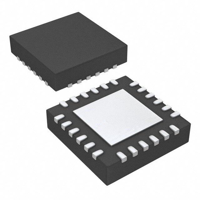
ICGOO电子元器件商城为您提供LM48901RL/NOPB由Texas Instruments设计生产,在icgoo商城现货销售,并且可以通过原厂、代理商等渠道进行代购。 LM48901RL/NOPB价格参考。Texas InstrumentsLM48901RL/NOPB封装/规格:线性 - 音頻放大器, Amplifier IC 4-Channel (Quad) Class D 36-DSBGA (3.5x3.24)。您可以下载LM48901RL/NOPB参考资料、Datasheet数据手册功能说明书,资料中有LM48901RL/NOPB 详细功能的应用电路图电压和使用方法及教程。
LM48901RL/NOPB是德州仪器(Texas Instruments)推出的一款音频功率放大器,属于线性音频放大器类别。该器件专为便携式音频设备设计,适用于需要高效、低功耗且高音质输出的应用场景。

典型应用场景包括:智能手机、平板电脑、便携式媒体播放器、笔记本电脑和小型蓝牙音箱等消费类电子产品。LM48901RL/NOPB采用D类放大架构,在保持高效率的同时提供清晰的音频输出,有效延长电池续航时间。其集成的立体声耳机放大器支持高质量音频回放,适合驱动32Ω耳机负载。

此外,该芯片具备良好的噪声抑制能力,内置爆音与咔嗒声抑制电路,可在开机、关机或切换信号时减少可闻噪声,提升用户体验。工作电压范围较宽,适应单电源供电环境,便于系统电源设计。

由于采用无铅封装(NOPB),符合环保要求,适用于对空间和功耗敏感的紧凑型设备。整体而言,LM48901RL/NOPB是一款高性能、低功耗的音频解决方案,广泛用于现代便携式音频设备中。
| 参数 | 数值 |
| 产品目录 | 集成电路 (IC)半导体 |
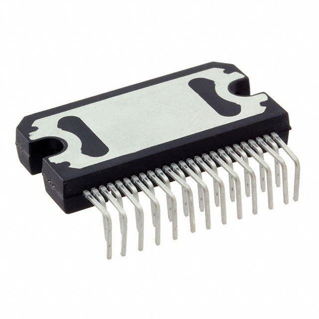
| 描述 | IC AMP AUDIO 2.8W D QUAD 36DSBGA音频放大器 Quad Class D Spatial Array |
| 产品分类 | |
| 品牌 | Texas Instruments |
| 产品手册 | http://www.ti.com/litv/SNAS520C |
| 产品图片 |
|
| rohs | 符合RoHS无铅 / 符合限制有害物质指令(RoHS)规范要求 |
| 产品系列 | 音频 IC,音频放大器,Texas Instruments LM48901RL/NOPBBoomer®, PowerWise® |
| 数据手册 | |
| 产品型号 | LM48901RL/NOPB |
| PCN组件/产地 | |
| THD+噪声 | 0.06 % |
| 不同负载时的最大输出功率x通道数 | 2.8W x 4 @ 4 欧姆 |
| 产品 | Audio Amplifiers |
| 产品种类 | 音频放大器 |
| 供应商器件封装 | 36-DSBGA |
| 共模抑制比—最小值 | 60 dB |
| 其它名称 | LM48901RL/NOPBCT |
| 包装 | 剪切带 (CT) |
| 商标 | Texas Instruments |
| 安装类型 | 表面贴装 |
| 安装风格 | SMD/SMT |
| 封装 | Reel |
| 封装/外壳 | 36-WFBGA |
| 封装/箱体 | uSMD-36 |
| 工作温度 | -40°C ~ 85°C (TA) |
| 工厂包装数量 | 250 |
| 最大工作温度 | + 85 C |
| 标准包装 | 1 |
| 特性 | 无噪音,差分输入,I²C,I²S,短路保护和热保护,关断 |
| 特色产品 | http://www.digikey.com/product-highlights/cn/zh/texas-instruments-lm48901-amplifier/1155 |
| 电压-电源 | 2.7 V ~ 5.5 V |
| 类 | Class-D |
| 类型 | Differential |
| 系列 | LM48901 |
| 输出功率 | 1.7 W |
| 输出类型 | 4-通道(四路) |


- 商务部:美国ITC正式对集成电路等产品启动337调查
- 曝三星4nm工艺存在良率问题 高通将骁龙8 Gen1或转产台积电
- 太阳诱电将投资9.5亿元在常州建新厂生产MLCC 预计2023年完工
- 英特尔发布欧洲新工厂建设计划 深化IDM 2.0 战略
- 台积电先进制程称霸业界 有大客户加持明年业绩稳了
- 达到5530亿美元!SIA预计今年全球半导体销售额将创下新高
- 英特尔拟将自动驾驶子公司Mobileye上市 估值或超500亿美元
- 三星加码芯片和SET,合并消费电子和移动部门,撤换高东真等 CEO
- 三星电子宣布重大人事变动 还合并消费电子和移动部门
- 海关总署:前11个月进口集成电路产品价值2.52万亿元 增长14.8%


PDF Datasheet 数据手册内容提取
LM48901 www.ti.com SNAS520C–OCTOBER2011–REVISEDJANUARY2012 LM48901 Quad Class D Spatial Array CheckforSamples:LM48901 FEATURES • Availableinspace-savingmicroSMDandLLP 1 packages • SpatialSoundProcessing 2 • I2SCompatibleInput APPLICATIONS • Differential-InputStereoADC • Laptops • EdgeRateControlReducesEMIwhile • Tablets PreservingAudioQualityandEfficiency • DesktopComputers • ParalleledOutputMode • SoundBars • ShortCircuitandThermalOverloadProtection • MultimediaDevices • Minimumexternalcomponents • MP3PlayerAccessories • ClickandPopsuppression • DockingStations • Micro-powershutdown DESCRIPTION The LM48901 is a quad Class D amplifier that utilizes Texas Instruments’ proprietary spatial sound processor to create an enhanced sound stage for portable multimedia devices. The Class D output stages feature Texas Instruments’ edge rate control (ERC) PWM architecture that significantly reduces RF emissions while preserving audioqualityandefficiency. TheLM48901’sflexibleI2Sinterfaceiscompatiblewithstandardserialaudiointerfaces.Astereodifferential-input ADCgivesthedevicetheabilitytoprocessanalogstereoaudiosignals. The LM48901 is configured through an I2C compatible interface and is capable of delivering 2.8W/channel of continuous output power into an 4Ω load with less than 10% THD+N. A 2.1 mode pairs two output drivers in parallel,increasingcurrentdrivefor4Ωloads. Output short circuit and thermal overload protection prevent the device from being damaged during fault conditions. Superior click and pop suppression eliminates audible transients on power-up/down and during shutdown.TheLM48901isavailableinspacesavingmicroSMDandLLPpackages. Table1.KeySpecifications VALUE UNIT SNR(A-Weighted) 87 dBA(typ) R =8Ω,THD+N≤10% 1.7 L OutputPower/channel,PV =5V W(typ) DD R =4Ω,THD+N≤10% 2.8 L THD+N 0.06%(typ) Efficiency/Channel 89%(typ) PSRRat217Hz 71 dB(typ) Shutdowncurrent1μA(typ) 1 µA(typ) 1 Pleasebeawarethatanimportantnoticeconcerningavailability,standardwarranty,anduseincriticalapplicationsof TexasInstrumentssemiconductorproductsanddisclaimerstheretoappearsattheendofthisdatasheet. Alltrademarksarethepropertyoftheirrespectiveowners. 2 PRODUCTIONDATAinformationiscurrentasofpublicationdate. Copyright©2011–2012,TexasInstrumentsIncorporated Products conform to specifications per the terms of the Texas Instruments standard warranty. Production processing does not necessarilyincludetestingofallparameters.
LM48901 SNAS520C–OCTOBER2011–REVISEDJANUARY2012 www.ti.com Typical Application 1.62V to 5.5V 2.7V to 5.5V 1.62V to 1.98V 2.7V to 5.5V 2.7V to 5.5V CS CS CS CS CS CS IOVDD PLLVDD DVDD AVDD PVDD PVDD OUT1+ H- INL+ BRIDGE OUT1- INL- INR+ 18-BIT STEREO ADC INR- REF OUT2+ 4.7 PF H- PLL BRIDGE OUT2- MCLK SCLK I2S SPATIAL WS INTERFACE PROCESSOR SDIO OUT3+ H- BRIDGE OUT3- I2C_EN I2C_EX SDA I2C SCL INTERFACE OUT4+ H- SHDN BRIDGE OUT4- IOGND DGND GND GND PGND PGND Figure1. TypicalAudioAmplifierApplicationCircuit 2 SubmitDocumentationFeedback Copyright©2011–2012,TexasInstrumentsIncorporated ProductFolderLinks:LM48901
LM48901 www.ti.com SNAS520C–OCTOBER2011–REVISEDJANUARY2012 1.62V to 5.5V 2.7V to 5.5V 1.62V to 1.98V 2.7V to 5.5V 2.7V to 5.5V CS CS CS CS CS CS IOVDD PLLVDD DVDD AVDD PVDD PVDD OUT1+ H- INL+ BRIDGE OUT1- INL- INR+ 18-BIT STEREO ADC INR- REF 4.7 PF OUT2+ H- PLL BRIDGE OUT2- MCLK SCLK I2S SPATIAL WS INTERFACE PROCESSOR SDIO OUT3+ H- BRIDGE OUT3- I2C_EN I2C_EX SDA I2C SCL INTERFACE OUT4+ H- SHDN BRIDGE OUT4- IOGND DGND GND GND PGND PGND Figure2. ChannelAudioAmplifierApplicationCircuit OnlyOUT2andOUT3canbeconfiguredinparallel.OUT1andOUT4cannotbeconfiguredinparallel. Copyright©2011–2012,TexasInstrumentsIncorporated SubmitDocumentationFeedback 3 ProductFolderLinks:LM48901
LM48901 SNAS520C–OCTOBER2011–REVISEDJANUARY2012 www.ti.com Connection Diagram microSMDPackage A OUT4+ PVDD OUT3+ OUT2+ PVDD OUT1+ B OUT4- PGND OUT3- OUT2- PGND OUT1- C IOVDD DVDD DGND AGND AVDD AVDD D SHDN I2C_EN IOGND AGND PLLVDD AVDD E I2C_EX WS SDA INR- INL- REF F MCLK SCLK SDIO SCL INR+ INL+ 1 2 3 4 5 6 Figure3. TopView 36–BumpmicroSMDMarking XYTT G02 Pin 1 Figure4. TopView XY=Datecode TT=Dietraceability G=BoomerFamily 02=LM48901RL 4 SubmitDocumentationFeedback Copyright©2011–2012,TexasInstrumentsIncorporated ProductFolderLinks:LM48901
LM48901 www.ti.com SNAS520C–OCTOBER2011–REVISEDJANUARY2012 SQPackage PGND OUT4- DGND IOVDD DVDD SHDN I2C_EN I2C_EX 2 1 0 9 8 7 6 5 3 3 3 2 2 2 2 2 OUT4+ 1 24 MCLK PVDD 2 23 WS OUT3- 3 22 SCLK OUT3+ 4 21 SDIO OUT2+ 5 20 SDA OUT2- 6 19 SCL PVDD 7 18 INR- OUT1+ 8 17 INR+ 9 10 11 12 13 14 15 16 PGND OUT1- GND DD1AV DD2AV REF INL- INL+ Figure5. TopView Table2.PinDescriptions BUMP PIN NAME DESCRIPTION A1 1 OUT4+ Channel4Non-InvertingOutput A2,A5 2,7 PVDD ClassDPowerSupply A3 4 OUT3+ Channel3Non-InvertingOutput.ConnecttoOUT2+inParallelMode. A4 5 OUT2+ Channel2Non-InvertingOutput.ConnecttoOUT3+inParallelMode. A6 8 OUT1+ Channel1Non-InvertingOutput B1 31 OUT4- Channel4InvertingOutput B2,B5 9,32 PGND PowerGround B3 3 OUT3- Channel3InvertingOutput.ConnecttoOUT2-inParallelMode. B4 6 OUT2- Channel2InvertingOutput.ConnecttoOUT3-inParallelMode. B6 10 OUT1- Channel1InvertingOutput C1 29 IOVDD DigitalInterfacePowerSupply C2 28 DVDD DigitalPowerSupply C3 30 DGND DigitalGround C4 11 AGND1 ModulatorAnalogGround C5 — AVDD3 ADCReferencePowerSupply C6 12 AVDD1 ModulatorAnalogPowerSupply.SettosamevoltageasPV formaximumheadroom. DD D1 27 SHDN ActiveLowShutdown.ConnecttoV fornormaloperation. DD D2 26 I2C_EN I2CEnableInput D3 30 IOGND DigitalInterfaceGround D4 — AGND2 ADCAnalogGround Copyright©2011–2012,TexasInstrumentsIncorporated SubmitDocumentationFeedback 5 ProductFolderLinks:LM48901
LM48901 SNAS520C–OCTOBER2011–REVISEDJANUARY2012 www.ti.com Table2.PinDescriptions(continued) BUMP PIN NAME DESCRIPTION D5 — PLLV PLLPowerSupply DD D6 13 AVDD2 ADCAnalogPowerSupply E1 25 I2C_EX I2CEnableOutput E2 23 WS I2SWordSelectInput E3 20 SDA I2CSerialDataInput E4 18 INR- RightChannelInvertingAnalogInput E5 15 INL- LeftChannelInvertingAnalogInput E6 14 REF ADCReferenceBypass F1 24 MCLK MasterClock F2 22 SCLK SerialClockInput F3 21 SDIO I2SSerialDataInput/Output F4 19 SCL I2CClockInput F5 17 INR+ RightChannelNon-InvertingAnalogInput F6 16 INL+ LeftChannelNon-InvertingAnalogInput Thesedeviceshavelimitedbuilt-inESDprotection.Theleadsshouldbeshortedtogetherorthedeviceplacedinconductivefoam duringstorageorhandlingtopreventelectrostaticdamagetotheMOSgates. Absolute Maximum Ratings (1) (2) SupplyVoltage AV ,PV ,PLV ,IOV (1) 6.0V DD DD DD DD SupplyVoltage,DV (1) 2.2V DD StorageTemperature −65°Cto+150°C InputVoltage −0.3VtoV +0.3V DD PowerDissipation (3) Internallylimited ESDSusceptibility (4) 2000V ESDSusceptibility (5) 150V JunctionTemperature 150°C ThermalResistance θ (microSMD) 26°C/W JA θ (LLP) 26°C/W JA θ (LLP) 2.6°C/W JC (1) “AbsoluteMaximumRatings”indicatelimitsbeyondwhichdamagetothedevicemayoccur,includinginoperabilityanddegradationof devicereliabilityand/orperformance.Functionaloperationofthedeviceand/ornon-degradationattheAbsoluteMaximumRatingsor otherconditionsbeyondthoseindicatedintheRecommendedOperatingConditionsisnotimplied.TheRecommendedOperating Conditionsindicateconditionsatwhichthedeviceisfunctionalandthedeviceshouldnotbeoperatedbeyondsuchconditions.All voltagesaremeasuredwithrespecttothegroundpin,unlessotherwisespecified. (2) TheElectricalCharacteristicstableslistguaranteedspecificationsunderthelistedRecommendedOperatingConditionsexceptas otherwisemodifiedorspecifiedbytheElectricalCharacteristicsConditionsand/orNotes.Typicalspecificationsareestimationsonlyand arenotguaranteed. (3) ThemaximumpowerdissipationmustbederatedatelevatedtemperaturesandisdictatedbyT ,θ ,andtheambienttemperature, JMAX JA T .ThemaximumallowablepowerdissipationisP =(T −T )/θ orthegiveninAbsoluteMaximumRatings,whicheveris A DMAX JMAX A JA lower. (4) Humanbodymodel,applicablestd.JESD22-A114C. (5) Machinemodel,applicablestd.JESD22-A115-A. Operating Ratings TemperatureRange T ≤T ≤T −40°C≤T ≤+85°C MIN A MAX A SupplyVoltage AV 2.7V≤AV ≤5.5V DD DD 6 SubmitDocumentationFeedback Copyright©2011–2012,TexasInstrumentsIncorporated ProductFolderLinks:LM48901
LM48901 www.ti.com SNAS520C–OCTOBER2011–REVISEDJANUARY2012 Operating Ratings (continued) PV 2.7V≤PV ≤5.5V DD DD PLLV 2.7V≤PLLV ≤5.5V DD DD IOV 1.62V≤IOV ≤5.5V DD DD DV 1.62V≤DV ≤1.98V DD DD Copyright©2011–2012,TexasInstrumentsIncorporated SubmitDocumentationFeedback 7 ProductFolderLinks:LM48901
LM48901 SNAS520C–OCTOBER2011–REVISEDJANUARY2012 www.ti.com ElectricalCharacteristicsPV =AV =5V,IOV =PLLV =3.3V,DV =1.8 (1) (2) DD DD DD DD DD ThefollowingspecificationsapplyforA =0dB,C =4.7µF,R =8Ω,f=1kHz,unlessotherwisespecified.Limitsapplyfor V REF L T =25°C. A LM48901 Units Symbol Parameter Conditions Min Typ Max (Limits) (2) (3) (2) AV AnalogSupplyVoltageRange (4) 2.7 5.5 V DD PV AmplifierSupplyVoltageRange (4) 2.7 5.5 V DD PLLV PLLSupplyVoltageRange 2.7 5.5 V DD IOV InterfaceSupplyVoltageRange 1.62 5.5 V DD DV DigitalSupplyVoltageRange 1.62 1.98 V DD LM48901RL 17.5 21 mA AI AnalogQuiescentSupplyCurrent DD LM48901SQ 19.2 22.3 mA AmplifierQuiescentSupply PI R =8Ω 5.25 8.25 mA DD Current L PLLI PLLQuiescentSupplyCurrent LM48901RL 1.5 mA DD QuiescentDigitalPowerSupply DI 5.5 6.2 mA DD Current ShutdownCurrent(Analog, I ShutdownEnabled 1 5 μA SD AmplifierandPLLSupplies) DI DigitalStandbyCurrent 30 μA STBY DI DigitalShutdownCurrent ShutdownEnabled 2 μA SD V DifferentialOutputOffsetVoltage V =0 –17 0 17 mV OS IN PowerUp(DeviceInitialization) 150 ms T Wake-upTime WU FromShutdown 30 ms f SwitchingFrequency f =48kHz 384 kHz SW S R =4Ω,THD+N=10% L f=1kHz,22kHzBW V =5V 2.8 W DD V =3.6V 1.4 W DD R =4Ω,THD+N=1% L f=1kHz,22kHzBW V =5V 2.2 W DD V =3.6V 1.2 W DD P OutputPower/Channel O R =8Ω,THD+N=10% L f=1kHz,22kHzBW V =5V 1.7 W DD V =3.6V 825 mW DD R =8Ω,THD+N=1% L f=1kHz,22kHzBW V =5V 1.0 1.3 W DD V =3.6V 650 mW DD (1) TheElectricalCharacteristicstableslistguaranteedspecificationsunderthelistedRecommendedOperatingConditionsexceptas otherwisemodifiedorspecifiedbytheElectricalCharacteristicsConditionsand/orNotes.Typicalspecificationsareestimationsonlyand arenotguaranteed. (2) R isaresistiveloadinserieswithtwoinductorstosimulateanactualspeakerload.ForR =8Ω,theloadis15μH+8Ω+15μH.ForR = L L L 4Ω,theloadis15μH+4Ω+15μH. (3) Datasheetmin/maxspecificationlimitsareguaranteedbydesign,test,orstatisticalanalysis. (4) MaintainPV andAV atthesamevoltagepotential. DD DD 8 SubmitDocumentationFeedback Copyright©2011–2012,TexasInstrumentsIncorporated ProductFolderLinks:LM48901
LM48901 www.ti.com SNAS520C–OCTOBER2011–REVISEDJANUARY2012 ElectricalCharacteristicsPV =AV =5V,IOV =PLLV =3.3V,DV =1.8(1)(2)(continued) DD DD DD DD DD ThefollowingspecificationsapplyforA =0dB,C =4.7µF,R =8Ω,f=1kHz,unlessotherwisespecified.Limitsapplyfor V REF L T =25°C. A LM48901 Units Symbol Parameter Conditions Min Typ Max (Limits) (2) (3) (2) R =4Ω,THD+N=10%,f=1kHz,22kHzBW L V =5V 3.2 W DD V =3.6V 1.6 W P OutputPower(ParallelMode) (5) DD O R =4Ω,THD+N=1%,f=1kHz,22kHzBW L V =5V 2.5 W DD V =3.6V 1.2 W DD THD+N TotalHarmonicDistortion+Noise P =500mW,f=1kHz,R =8Ω 0.06 % O L V =200mV sine,InputsACGND,C =1μF RIPPLE P-P IN f =217Hz,AppliedtoPV 67 dB RIPPLE DD f =217Hz,AppliedtoDV 54 dB RIPPLE DD PowerSupplyRejectionRatio PSRR f =1kHz,AppliedtoPV 66 dB (ADCPath) RIPPLE DD f =1kHz,AppliedtoDV 54 dB RIPPLE DD f =10kHz,AppliedtoPV 57 dB RIPPLE DD f =10kHz,AppliedtoDV 52 dB RIPPLE DD V =200mV sine,Inputs–120dBFS RIPPLE P-P f =217Hz,AppliedtoPV 71 dB RIPPLE DD f =217Hz,AppliedtoDV 58 dB RIPPLE DD PowerSupplyRejectionRatio PSRR (I2SPath) fRIPPLE=1kHz,AppliedtoPVDD 69 dB f =1kHz,AppliedtoDV 57 dB RIPPLE DD f =10kHz,AppliedtoPV 70 dB RIPPLE DD f =10kHz,AppliedtoDV 55 dB RIPPLE DD V =1V ,f =217Hz, CMRR CommonModeRejectionRatio RIPPLE P-P RIPPLE 60 dB A =0dB V V =5V,P =1.1W 89 % DD O η Efficiency/Channel V =3.6V,P =400mW 87 % DD O V =5V,P =1.1W 87 % DD O η Efficiency V =3.6V,P =400mW 86 % DD O ADCInput,P =1W 85 dB O SNR Signal-to-Noise-Ratio I2SInput,P =1W 87 dB O CommonModeInputVoltage CMVR 5 V Range InputsACGND,A-weighted, 130 μV εOS OutputNoise AV=0dB I2SInput 72 μV X Crosstalk 75 dB TALK (5) OnlyOUT2andOUT3canbeconfiguredinParallelMode. Copyright©2011–2012,TexasInstrumentsIncorporated SubmitDocumentationFeedback 9 ProductFolderLinks:LM48901
LM48901 SNAS520C–OCTOBER2011–REVISEDJANUARY2012 www.ti.com I2C Interface Characteristics (1) (2) ThefollowingspecificationsapplyforR =1kΩtoIOV ,unlessotherwisespecified.LimitsapplyforT =25°C. PU DD A LM48901 Symbol Parameter Conditions Min Typ Max Units (3) (4) (3) VIH LogicInputHighThreshold SDA,SCL 0.7*IOV V DD VIL LogicInputLowThreshold SDA,SCL 300 mV VOL LogicOutputLowThreshold SDA,ISDA=3.6mA 0.35 V IOH LogicOutputHighCurrent SDA,SCL 2 uA SCLFrequency 400 kHz HoldTime 1 0.6 µs (repeatedSTARTCondition) 2 ClockLowTime 1.3 µs 3 ClockHighTime 600 ns SetupTimeforRepeatedSTART 4 600 ns condition 5 DataHoldTime Output 300 900 ns 6 DataSetupTime 100 ns 7 SDARiseTime 300 ns 8 SDAFallTime 300 ns 9 SetupTimeforSTOPCondition 600 ns BusFreeTimeBetweenSTOP 10 1.3 µs andSTARTCondition (1) “AbsoluteMaximumRatings”indicatelimitsbeyondwhichdamagetothedevicemayoccur,includinginoperabilityanddegradationof devicereliabilityand/orperformance.Functionaloperationofthedeviceand/ornon-degradationattheAbsoluteMaximumRatingsor otherconditionsbeyondthoseindicatedintheRecommendedOperatingConditionsisnotimplied.TheRecommendedOperating Conditionsindicateconditionsatwhichthedeviceisfunctionalandthedeviceshouldnotbeoperatedbeyondsuchconditions.All voltagesaremeasuredwithrespecttothegroundpin,unlessotherwisespecified. (2) TheElectricalCharacteristicstableslistguaranteedspecificationsunderthelistedRecommendedOperatingConditionsexceptas otherwisemodifiedorspecifiedbytheElectricalCharacteristicsConditionsand/orNotes.Typicalspecificationsareestimationsonlyand arenotguaranteed. (3) Datasheetmin/maxspecificationlimitsareguaranteedbydesign,test,orstatisticalanalysis. (4) TypicalvaluesrepresentmostlikelyparametricnormsatT =+25ºC,andattheRecommendedOperationConditionsatthetimeof A productcharacterizationandarenotguaranteed. 10 SubmitDocumentationFeedback Copyright©2011–2012,TexasInstrumentsIncorporated ProductFolderLinks:LM48901
LM48901 www.ti.com SNAS520C–OCTOBER2011–REVISEDJANUARY2012 I2S Timing Characteristics (1) (2) ThefollowingspecificationsapplyforDV =1.8V,unlessotherwisespecified.LimitsapplyforT =25°C. DD A LM48901 Units Symbol Parameter Conditions Min Typ Max (Limits) (3) (4) (3) t MCLKPulseWidthLow 16 ns MCLKL t MCLKPulseWidthHigh 16 ns MCLKH t MCLKPeriod 27 ns MCLKY t SCLKrisetime 3 ns BCLKR t SCLKfalltime 3 ns BCLKCF t SCLKDutyCycle 50 % BCLKDS LRCPropagationDelayfrom T 10 ns DL SCLKfallingedge DATASetupTimetoSCLKRising T 10 ns DST Edge DATAHoldTimefromSCLK T 10 ns DHT RisingEdge (1) TheElectricalCharacteristicstableslistguaranteedspecificationsunderthelistedRecommendedOperatingConditionsexceptas otherwisemodifiedorspecifiedbytheElectricalCharacteristicsConditionsand/orNotes.Typicalspecificationsareestimationsonlyand arenotguaranteed. (2) R isaresistiveloadinserieswithtwoinductorstosimulateanactualspeakerload.ForR =8Ω,theloadis15μH+8Ω+15μH.ForR = L L L 4Ω,theloadis15μH+4Ω+15μH. (3) Datasheetmin/maxspecificationlimitsareguaranteedbydesign,test,orstatisticalanalysis. (4) TypicalvaluesrepresentmostlikelyparametricnormsatT =+25ºC,andattheRecommendedOperationConditionsatthetimeof A productcharacterizationandarenotguaranteed. Copyright©2011–2012,TexasInstrumentsIncorporated SubmitDocumentationFeedback 11 ProductFolderLinks:LM48901
LM48901 SNAS520C–OCTOBER2011–REVISEDJANUARY2012 www.ti.com Typical Performance Characteristics THD+N THD+N vs vs FREQUENCY FREQUENCY V =3.6V,P =500mW, V =5V,P =925mW, DD OUT DD OUT R =8Ω,ADCInput R =8Ω,ADCInput L L 100 100 10 10 %) %) +N ( 1 +N ( 1 D D H H T T 0.1 0.1 SINGLE CHANNEL SINGLE CHANNEL 0.01 0.01 0.01 0.1 1 10 100 0.01 0.1 1 10 100 FREQUENCY (kHz) FREQUENCY (kHz) THD+N THD+N vs vs FREQUENCY FREQUENCY V =3.6V,P =7505mW, V =5V,P =1.3W, DD OUT DD OUT R =4Ω,ADCInput R =4Ω,ADCInput L L 100 100 10 10 %) %) +N ( 1 +N ( 1 D D H H T T 0.1 0.1 SINGLE CHANNEL SINGLE CHANNEL 0.01 0.01 0.01 0.1 1 10 100 0.01 0.1 1 10 100 FREQUENCY (kHz) FREQUENCY (kHz) THD+N THD+N vs vs FREQUENCY FREQUENCY V =3.6V,P =900mW, V =3.6V,P =450mW, DD OUT DD OUT R =4Ω,ADCInput R =8Ω,I2SInput L L 100 100 10 10 %) %) +N ( 1 +N ( 1 D D H H T T 0.1 0.1 PARALLEL MODE SINGLE CHANNEL 0.01 0.01 0.01 0.1 1 10 100 0.01 0.1 1 10 100 FREQUENCY (kHz) FREQUENCY (kHz) 12 SubmitDocumentationFeedback Copyright©2011–2012,TexasInstrumentsIncorporated ProductFolderLinks:LM48901
LM48901 www.ti.com SNAS520C–OCTOBER2011–REVISEDJANUARY2012 Typical Performance Characteristics (continued) THD+N THD+N vs vs FREQUENCY FREQUENCY V =5V,P =950mW, V =3.6V,P =750mW, DD OUT DD OUT R =8Ω,I2SInput R =4Ω,I2SInput L L 100 100 10 10 %) %) +N ( 1 +N ( 1 D D H H T T 0.1 0.1 SINGLE CHANNEL SINGLE CHANNEL 0.01 0.01 0.01 0.1 1 10 100 0.01 0.1 1 10 100 FREQUENCY (kHz) FREQUENCY (kHz) THD+N THD+N vs vs FREQUENCY FREQUENCY V =5V,P =1.65W, V =3.6V,P =850mW, DD OUT DD OUT R =4Ω,I2SInput R =4Ω,I2SInput L L 100 100 10 10 %) %) +N ( 1 +N ( 1 D D H H T T 0.1 0.1 SINGLE CHANNEL PARALLEL MODE 0.01 0.01 0.01 0.1 1 10 100 0.01 0.1 1 10 100 FREQUENCY (kHz) FREQUENCY (kHz) THD+N vs THD+N FREQUENCY vs V =5V,P =1.8W, OUTPUTPOWER DD OUT R =4Ω,I2SInput R =8Ω,f=1kHz,ADCInput L L 100 100 VDD = 5V 10 10 VDD = 3.6V %) %) D+N ( 1 D+N ( 1 H H T T 0.1 0.1 PARALLEL MODE SINGLE CHANNEL 0.01 0.01 0.01 0.1 1 10 100 0.001 0.01 0.1 1 10 FREQUENCY (kHz) OUTPUT POWER (W) Copyright©2011–2012,TexasInstrumentsIncorporated SubmitDocumentationFeedback 13 ProductFolderLinks:LM48901
LM48901 SNAS520C–OCTOBER2011–REVISEDJANUARY2012 www.ti.com Typical Performance Characteristics (continued) THD+N THD+N vs vs OUTPUTPOWER OUTPUTPOWER R =4Ω,f=1kHz,ADCInput,Singlechannel R =8Ω,f=1kHz,ADCInput L L 100 100 VDD = 5V VDD = 5V 10 VDD = 3.6V 10 VDD = 3.6V %) %) +N ( 1 +N ( 1 D D H H T T 0.1 0.1 SINGLE CHANNEL ALL CHANNELS 0.01 0.01 0.001 0.01 0.1 1 10 0.001 0.01 0.1 1 10 OUTPUT POWER (W) OUTPUT POWER (W) THD+N THD+N vs vs OUTPUTPOWER OUTPUTPOWER R =4Ω,f=1kHz,ADCInput,Allchannels R =4Ω,f=1kHz,ADCInput,Parallelmode L L 100 100 VDD = 5V VDD = 5V 10 10 VDD = 3.6V VDD = 3.6V %) %) +N ( 1 +N ( 1 D D H H T T 0.1 0.1 ALL CHANNELS PARALLEL MODE 0.01 0.01 0.001 0.01 0.1 1 10 0.001 0.01 0.1 1 10 OUTPUT POWER (W) OUTPUT POWER (W) THD+N THD+N vs vs OUTPUTPOWER OUTPUTPOWER R =8Ω,f=1kHz,I2SInput,Singlemode R =4Ω,f=1kHz,I2SInput,Singlechannel L L 100 100 VDD = 5V VDD = 5V 10 VDD = 3.6V 10 VDD = 3.6V %) %) +N ( 1 +N ( 1 D D H H T T 0.1 0.1 SINGLE CHANNEL SINGLE CHANNEL 0.01 0.01 0.001 0.01 0.1 1 10 0.001 0.01 0.1 1 10 OUTPUT POWER (W) OUTPUT POWER (W) 14 SubmitDocumentationFeedback Copyright©2011–2012,TexasInstrumentsIncorporated ProductFolderLinks:LM48901
LM48901 www.ti.com SNAS520C–OCTOBER2011–REVISEDJANUARY2012 Typical Performance Characteristics (continued) THD+N THD+N vs vs OUTPUTPOWER OUTPUTPOWER R =8Ω,f=1kHz,I2SInput,Allchannels R =4Ω,f=1kHz,I2SInput,Allchannels L L 100 100 VDD = 5V VDD = 5V 10 10 VDD = 3.6V VDD = 3.6V %) %) +N ( 1 +N ( 1 D D H H T T 0.1 0.1 ALL CHANNELS ALL CHANNELS 0.01 0.01 0.001 0.01 0.1 1 10 0.001 0.01 0.1 1 10 OUTPUT POWER (W) OUTPUT POWER (W) THD+N THD+N vs vs OUTPUTPOWER OUTPUTPOWER R =4Ω,f=1kHz,I2SInput,Allchannels R =4Ω,f=1kHz,I2SInput,Parallelmode L L 100 100 VDD = 5V VDD = 5V 10 10 VDD = 3.6V VDD = 3.6V %) %) +N ( 1 +N ( 1 D D H H T T 0.1 0.1 ALL CHANNELS PARALLEL MODE 0.01 0.01 0.001 0.01 0.1 1 10 0.001 0.01 0.1 1 10 OUTPUT POWER (W) OUTPUT POWER (W) EFFICIENCY EFFICIENCY vs vs OUTPUTPOWER OUTPUTPOWER R =8Ω,f=1kHz,ADCInput,Allchannels R =4Ω,f=1kHz,ADCInput,Allchannels L L 100 100 PVDD = 3.6V PVDD = 5V 90 90 80 80 70 PVDD = 5V 70 %) %) PVDD = 3.6V EFFICIENCY ( 456000 EFFICIENCY ( 456000 30 30 20 20 10 10 0 0 0 500 1000 1500 2000 0 500 1000 1500 2000 2500 OUTPUT POWER (mW) OUTPUT POWER (mW) Copyright©2011–2012,TexasInstrumentsIncorporated SubmitDocumentationFeedback 15 ProductFolderLinks:LM48901
LM48901 SNAS520C–OCTOBER2011–REVISEDJANUARY2012 www.ti.com Typical Performance Characteristics (continued) POWERDISSIPATION POWERDISSIPATION vs vs OUTPUTPOWER OUTPUTPOWER R =8Ω,f=1kHz,ADCInput R =4Ω,f=1kHz,ADCInput L L 1000 3000 W) 890000 VDD = 5V W)2500 VDD = 5V m m ON ( 700 ON (2000 DISSIPATI 456000000 DISSIPATI1500 VDD = 3.6V WER 300 WER 1000 O VDD = 3.6V O P 200 P 500 100 ALL CHANNELS ALL CHANNELS 0 0 0 500 1000 1500 2000 0 500 1000 1500 2000 2500 OUTPUT POWER (mW) OUTPUT POWER (mW) OUTPUTPOWER OUTPUTPOWER vs vs SUPPLYVOLTAGE SUPPLYVOLTAGE R =4Ω,f=1kHz,ADCInput,Singlemode R =4Ω,f=1kHz,ADCInput,Parallelmode L L 4 4 SINGLE CHANNEL PARALLEL MODE 3.5 3.5 W) 3 W) 3 ER ( 2.5 THD + N = 10% ER ( 2.5 THD + N = 10% W W O O P 2 P 2 UT UT UTP 1.5 UTP 1.5 O 1 O 1 THD + N = 1% THD + N = 1% 0.5 0.5 0 0 2.5 3 3.5 4 4.5 5 5.5 2.5 3 3.5 4 4.5 5 5.5 SUPPLY VOLTAGE (V) SUPPLY VOLTAGE (V) PSRR OUTPUTPOWER vs vs FREQUENCY SUPPLYVOLTAGE PV =5V,V =200mV ,R =8Ω, DD RIPPLE P-P L R =8Ω,f=1kHz,ADCInput,Singlechannel ADCMode,ADCinput=ACGND L 2.5 0 SINGLE CHANNEL -10 2 W) -20 R ( THD + N = 10% -30 WE 1.5 B) PUT PO 1 PSRR (d --5400 T U -60 O 0.5 THD + N = 1% -70 -80 0 -90 2.5 3 3.5 4 4.5 5 5.5 0.01 0.1 1 10 100 SUPPLY VOLTAGE (V) FREQUENCY (kHz) 16 SubmitDocumentationFeedback Copyright©2011–2012,TexasInstrumentsIncorporated ProductFolderLinks:LM48901
LM48901 www.ti.com SNAS520C–OCTOBER2011–REVISEDJANUARY2012 Typical Performance Characteristics (continued) PSRR PSRR vs vs FREQUENCY FREQUENCY DV =1.8V,V =200mV ,R =8Ω, PV =5V,V =200mV ,R =8Ω, DD RIPPLE P-P L DD RIPPLE P-P L ADCMode,ADCinput=ACGND I Smode,I Sinput=–120dBFS 2 2 0 0 -10 -10 -20 -20 -30 PSRR (dB) -30 PSRR (dB) --5400 -40 -60 -70 -50 -80 -60 -90 0.01 0.1 1 10 100 0.01 0.1 1 10 100 FREQUENCY (kHz) FREQUENCY (kHz) PSRR PSRR vs vs FREQUENCY FREQUENCY DV =1.8V,V =200mV ,R =8Ω, V =200mV ,R =8Ω, DD RIPPLE P-P L RIPPLE P-P L I Smode,I Sinput=–120dBFS ADCmode 2 2 0 0 -10 -10 -20 -20 PSRR (dB) -30 PSRR (dB) --4300 -40 -50 -50 -60 -60 -70 0.01 0.1 1 10 100 0.01 0.1 1 10 100 FREQUENCY (kHz) FREQUENCY (kHz) SUPPLYCURRENT vs SUPPLYCURRENT SUPPLYVOLTAGE(PV ) vs DD R =Open,ADCmode, SUPPLYVOLTAGE(AV ) L DD Allchannelsenabled R =Open L 5 20 ADC MODE SUPPLY CURRENT (A)P 234 SUPPLY CURRENT (A)P 11505 I2S MODE 1 0 0 2.5 3 3.5 4 4.5 5 5.5 2.5 3 3.5 4 4.5 5 5.5 SUPPLY VOLTAGE (V) SUPPLY VOLTAGE (V) Copyright©2011–2012,TexasInstrumentsIncorporated SubmitDocumentationFeedback 17 ProductFolderLinks:LM48901
LM48901 SNAS520C–OCTOBER2011–REVISEDJANUARY2012 www.ti.com Typical Performance Characteristics (continued) SUPPLYCURRENT SUPPLYCURRENT vs vs SUPPLYVOLTAGE(PLV ) SUPPLYVOLTAGE(DV ) DD DD ADCmode,Allchannelsenabled R =Open L 5 20 A)P 4 A)P 15 T ( T ( N N E 3 E R R R R U U 10 C C ADC MODE LY 2 LY P P UP UP I2S MODE S S 5 1 0 0 2.5 3 3.5 4 4.5 5 5.5 1.6 1.7 1.8 1.9 2 SUPPLY VOLTAGE (V) SUPPLY VOLTAGE (V) SHUTDOWNCURRENT SHUTDOWNCURRENT vs vs SUPPLYVOLTAGE SUPPLYVOLTAGE(DV ) DD 1 2 NT (A)P 0.8 NT (A)P 1.5 RE 0.6 RE R R U U 1 C C SUPPLY 0.4 SUPPLY 0.5 0.2 0 0 2.5 3 3.5 4 4.5 5 5.5 1.6 1.7 1.8 1.9 2 SUPPLY VOLTAGE (V) SUPPLY VOLTAGE (V) OUTPUTNOISE OUTPUTNOISE VS VS FREQUENCY FREQUENCY PV =5V,R =8Ω, DV =1.8V,R =8Ω, DD L DD L ADCmode,ADCInput=ACGND I2Smode,I2SInput=–120dBFS 200 200 150 150 )V )V P P E ( E ( S S OI 100 OI 100 N N T T U U P P T T U U O 50 O 50 0 0 0.01 0.1 1 10 100 0.01 0.1 1 10 100 FREQUENCY (Hz) FREQUENCY (Hz) 18 SubmitDocumentationFeedback Copyright©2011–2012,TexasInstrumentsIncorporated ProductFolderLinks:LM48901
LM48901 www.ti.com SNAS520C–OCTOBER2011–REVISEDJANUARY2012 Application Information I2CCOMPATIBLEINTERFACE TheLM48901iscontrolledthroughanI2Ccompatibleserialinterfacethatconsistsofaserialdataline(SDA)and a serial clock (SCL). The clock and data lines are bi-directional (open drain). The LM48901 can communicate at clock rates up to 400kHz. Figure 6 shows the I2C interface timing diagram. Data on the SDA line must be stable during the HIGH period of SCL. The LM48901 is a transmit/receive device, and can act as the I2C master, generating the SCL signal. Each transmission sequence is framed by a START condition and a STOP condition Figure7. Due to the number of data registers, the LM48901 employs a page mode scheme. Each data write consists of 7, 8 bit data bytes, device address (1 byte), 16 bit register address (2 bytes), and 32 bit register data (4 bytes). Each byte is followed by an acknowledge pulse Figure 8. Single byte read and write commands are ignored. The LM48901deviceaddressis0110000X. Figure6. I2CTimingDiagram SDA SCL S P START condition STOP condition Figure7. StartandStopDiagram WRITESEQUENCE The example write sequence is shown in Figure 8. The START signal, the transition of SDA from HIGH to LOW whileSDAisHIGH,isgenerated,alteringalldevicesonthebusthatadeviceaddressisbeingwrittentothebus. The 7-bit device address is written to the bus, most significant bit (MSB) first, followed by the R/W bit (R/W = 0 indicating the master is writing to the LM48901). The data is latched in on the rising edge of the clock. Each addressbitmustbestablewhileSDAisHIGH.AftertheR/W\bitistransmitted,themasterdevicereleasesSDA, during which time, an acknowledge clock pulse is generated by the slave device. If the LM48901 receives the correctaddress,thedevicepullstheSDAlinelow,generatingandacknowledgebit(ACK). Once the master device registers the ACK bit, the first 8-bit register address word is sent, MSB first [15:8]. Each data bit should be stable while SCL is HIGH. After the first 8-bit register address is sent, the LM48901 sends another ACK bit. Upon receipt of acknowledge, the second 8-bit register address word is sent [7:0], followed by another ACK bit. The register data is sent, 8-bits at a time, MSB first in the following order [7:0], [15:8], [23:16], [31:24]. Each 8-bit word is followed by an ACK, upon receipt of which the successive 8-bit word is sent. Following the acknowledgement of the last register data word [31:24], the master issues a STOP bit, allowing SDAtogohighwhileSDAishigh. Copyright©2011–2012,TexasInstrumentsIncorporated SubmitDocumentationFeedback 19 ProductFolderLinks:LM48901
LM48901 SNAS520C–OCTOBER2011–REVISEDJANUARY2012 www.ti.com SCL SDA START MSB DEVICE ADDRESS LSB W ACK REGISTER ADDRESS [15:8] ACK REGISTER ADDRESS [7:0] ACK SCL SDA REGISTER DATA [7:0] ACK REGISTER DATA [15:8] ACK REGISTER DATA [23:16] ACK SCL SDA REGISTER DATA [31:24] ACK STOP Figure8. ExampleI2CWriteSequence READSEQUENCE The example read sequence is shown in Figure 9. The START signal, the transition of SDA from HIGH to LOW whileSDAisHIGH,isgenerated,alteringalldevicesonthebusthatadeviceaddressisbeingwrittentothebus. The 7-bit device address is written to the bus, followed by the R/W = 0. After the R/W bit is transmitted, the master device releases SDA, during which time, an acknowledge clock pulse is generated by the slave device. If the LM48901 receives the correct address, the device pulls the SDA line low, generating and acknowledge bit (ACK). Once the master device registers the ACK bit, the first 8-bit register address word is sent, MSB first [15:8], followed by and ACK from the LM48901. Upon receipt of the acknowledge, the second 8-bit register address word is sent [7:0], followed by another ACK bit. Following the acknowledgement of the last register address, the master initiates a REPEATED START, followed by the 7-bit device address, followed by R/W = 1 (R/W = 1 indicating the master wants to read data from the LM48901). The LM48901 sends an ACK, followed by the selected register data. The register data is sent, 8-bits at a time, MSB first in the following order [7:0], [15:8], [23:16], [31:24]. Each 8-bit word is followed by an ACK, upon receipt of which the successive 8-bit word is sent. Following the acknowledgement of the last register data word [31:24], the master issues a STOP bit, allowing SDAtogohighwhileSDAishigh. SCL SDA START MSB DEVICE ADDRESS LSB W ACK REGISTER ADDRESS [15:8] ACK REGISTER ADDRESS [7:0] ACK SCL SDA START MSB DEVICE ADDRESS LSB R ACK REGISTER DATA [7:0] ACK REGISTER DATA [15:8] ACK SCL SDA REGISTER DATA [23:16] ACK REGISTER DATA [31:24] ACK STOP Figure9. ExampleI2CReadSequence I2SDATAFORMAT The LM48901 supports three I2S formats: Normal Mode Figure 10, Left Justified Mode Figure 11, and Right Justified Mode Figure 12. In Normal Mode, the audio data is transmitted MSB first, with the unused bits following the LSB. In Left Justified Mode, the audio data format is similar to the Normal Mode, without the delay between the LSB and the change in I2S_WS. In Right Justified Mode, the audio data MSB is transmitted after a delay of a presetnumberofbits. 20 SubmitDocumentationFeedback Copyright©2011–2012,TexasInstrumentsIncorporated ProductFolderLinks:LM48901
LM48901 www.ti.com SNAS520C–OCTOBER2011–REVISEDJANUARY2012 I2S_CLK I2S_WS I2S_DATA X 23 22 21 1 0 X X 23 22 21 1 0 X X LEFT CHANNEL DATA WORD RIGHT CHANNEL DATA WORD Figure10. I2SNormalInputFormat I2S_CLK I2S_WS I2S_DATA 23 22 21 20 2 1 0 X 23 22 21 20 3 2 1 0 X LEFT CHANNEL DATA WORD RIGHT CHANNEL DATA WORD Figure11. I2SLeftJustifiedInputFormat I2S_CLK I2S_WS I2S_DATA X X 23 22 2 1 0 X X 23 22 2 1 0 LEFTCHANNELDATAWORD RIGHTCHANNELDATAWORD Figure12. I2SRightJustifiedInputFormat MEMORYORGANIZATION TheLM48901memoryisorganizedintothreemainregions:a32-bitwideCoefficientSpacethatholdsthespatial coefficients, a 32-bit wide Register Space that holds the device configuration settings, and a 48-bit wide Audio Sample Space that holds the current audio data sampled from either the ADCs or the I2S interface, organized as showninFigure13. 0X7FFh INPUT SAMPLE MEMORY 0x700h - 0x7FFh: Array Filter Sample Memory (48-BIT) 0x600h - 0x67Fh: Pre-Filter Sample Memory 0X600h 0x520h - 0x527h: Analog Control Registers REGISTER SPACE 0x510h - 0x51Fh: System Control Registers (32-BIT) 0x500h - 0x50Fh: Filter Control Registers 0X500h COEFFICIENT SPACE 0x400h - 0x4FFh: Pre-Filter Coefficients (32-BIT) 0x000h - 0x3FFh: Array Coefficients 0X000h Figure13. LM48901MemoryOrganization Copyright©2011–2012,TexasInstrumentsIncorporated SubmitDocumentationFeedback 21 ProductFolderLinks:LM48901
LM48901 SNAS520C–OCTOBER2011–REVISEDJANUARY2012 www.ti.com COEFFICIENTMEMORY The device must be in Debug mode in order to write to the Coefficient memory. Set Bit 7 (DBG_ENABLE) in Filter Debug Register 1 (0x504h) = 1 to enable Debug mode. The Coefficient Memory Space is organized as follows. Table3.CoefficientMemorySpace REGISTERADDRESS REGISTERCONTENTS (31:16) (15:0) 256x16bitArrayTaps 256x16bitArrayTaps 0x000h-0x0FFh (RightInputtoOUT4) (LeftInputtoOUT4) 256x16bitArrayTaps 256x16bitArrayTaps 0x100h-0x1FFh (RightInputtoOUT3) (LeftInputtoOUT3) 256x16bitArrayTaps 256x16bitArrayTaps 0x200h-0x2FFh (RightInputtoOUT2) (LeftInputtoOUT2) 256x16bitArrayTaps 256x16bitArrayTaps 0x300h-0x3FFh (RightInputtoOUT1) (LeftInputtoOUT1) C2128x16bitPrefilterTaps C0128x16bitPrefilterFIRTaps 0x400h-0x47Eh(EVEN) (RighttoRight) (LefttoLeft) C3128x16bitPrefilterTaps C1128x16bitPrefilterFIRTaps 0x441h-0x47Fh(ODD) (RighttoLeft) (LefttoRight) CONTROLREGISTERS Table4.RegisterMap Register Register Default 7 6 5 4 3 2 1 0 Name Address Value 0x500h 0xFFh ARRAY_TAP [7:0] 0x500h[15:8] 0xFFh UNUSED PRE_TAP FILTER CONTROL 0x500h[23:16] 0xE4h CH4_SEL CH3_SEL CH2_SEL CH1_SEL ARRAY_ PRE_ ARRAY_ PRE_ 0x500h[31:24] 0x31h UNUSED ENABLE ENABLE BYPASS BYPASS 0x501h 0x00h G1_GAIN COMP_TH [7:0] FILTER 0x501h[15:8] 0x00h UNUSED POST_GAIN UNUSED COMP_RATIO COMP1 0x501h[23:16] 0x00h ARRAY_COMP_SELECT 0x501h[31:24] 0x00h UNUSED 0x502h G1_GAIN COMP_TH [7:0] 0x00h FILTER 0x502h[15:8] 0x00h UNUSED POST_GAIN UNUSED COMP_RATIO COMP2 0x502h[23:16] 0x00h G1_GAIN COMP_TH 0x502h[31:24] 0x00h UNUSED POST_GAIN UNUSED COMP_RATIO 0x503h 0xFFh DBG_DATA[7:0] [7:0] 0x503h[15:8] 0xFFh DBG_DATA[15:8] FILTER DEBUG0 0x503h[23:16] 0xFFh DBG_DATA[23:16] DBG_ 0x503h[31:24] 0xFFh UNUSED STEP 0x504h DBG_ STEP_ FILTER_ 0xFFh UNUSED ACC_ADDR [7:0] ENABLE ENABLE SELECT FILTER 0x504h[15:8] 0xFFh UNUSED DEBUG1 0x504h[23:16] 0xFFh UNUSED 0x504h[31:24] 0xFFh UNUSED 22 SubmitDocumentationFeedback Copyright©2011–2012,TexasInstrumentsIncorporated ProductFolderLinks:LM48901
LM48901 www.ti.com SNAS520C–OCTOBER2011–REVISEDJANUARY2012 Table4.RegisterMap(continued) Register Register Default 7 6 5 4 3 2 1 0 Name Address Value 0x505h 0x00h COUNT1_MODE CH_SEL [7:0] FILTER 0x505h[15:8] 0x80h CLEAR UNUSED COUNT2_MODE STATS 0x505h[23:16] 0x00h COUNT1_MODE CH_SEL 0x505h[31:24] 0x80h CLEAR UNUSED COUNT2_MODE 0x508h 0x7Fh TAP_LENGTH [7:0] FILTERTAP (READ- 0x508h[15:8] 0x00h UNUSED ONLY) 0x508h[23:16] 0x00h UNUSED 0x508h[31:24] 0x00h UNUSED 0x509h 0x00h DBG_ACCL[7:0] ACCUML [7:0] DEBUG 0x509h[15:8] 0x00h DBG_ACCL[15:8] (READ- ONLY) 0x509h[23:16] 0x00h DBG_ACCL[23:16] 0x509h[31:24] 0x00h DBG_ACCL[31:24] 0x50Ah 0x00h DBG_ACCH ACCUMH [7:0] DEBUG 0x50Ah[15:8] 0x00h BDG_ACCH (READ- ONLY) 0x50Ah[23:16] 0x00h UNUSED 0x50Ah[31:24] 0x00h UNUSED 0x50Bh 0x00h DBG_SAT[7:0] [7:0] DBGSAT (READ- 0x50Bh[15:8] 0x00h DBG_SAT[15:8] ONLY) 0x50Bh[23:16] 0x00h DBG_SAT[23:16] 0x50Bh[31:24] 0x00h UNUSED 0x50Ch 0x00h COUNT[7:0] STAT [7:0] PCNT1 0x50Ch[15:8] 0x00h COUNT[15:8] (READ- ONLY) 0x50Ch[23:16] 0x00h COUNT[23:16] 0x50Ch[31:24] 0x00h OVF COUNT[30:24] 0x50Dh 0x00h COUNT[7:0] STAT [7:0] PCNT2 0x50Dh[15:8] 0x00h COUNT[15:8] (READ- ONLY) 0x50Dh[23:16] 0x00h COUNT[23:16] 0x50Dh[31:24] 0x00h OVF COUNT[30:24] 0x50Eh 0x00h COUNT[7:0] STAT [7:0] ACNT1 0x50Eh[15:8] 0x00h COUNT[15:8] (READ- ONLY) 0x50Eh[23:16] 0x00h COUNT[23:16] 0x50Eh[31:24] 0x00h OVF COUNT[30:24] 0x50Fh 0x00h COUNT[7:0] STAT [7:0] ACNT2 0x50Fh[15:8] 0x00h COUNT[15:8] (READ- ONLY) 0x50Fh[23:16] 0x00h COUNT[23:16] 0x50Fh[31:24] 0x00h OVF COUNT[30:24] CONFIG 0x530h 0x30h _CLK_ DEVICE_ID [7:0] ENABLE ALTID_ SYS 0x530h[15:8] 0x00h ALT_DEVICE_ID CONFIG ENABLE CL_ 0x530h[23:16] 0x8Ch UNUSED CL_PAGE CL_W CL_REQ ENABLE MBIST1_ MBIST0_ 0x530h[31:24] 0x00h UNUSED ENABLE ENABLE Copyright©2011–2012,TexasInstrumentsIncorporated SubmitDocumentationFeedback 23 ProductFolderLinks:LM48901
LM48901 SNAS520C–OCTOBER2011–REVISEDJANUARY2012 www.ti.com Table4.RegisterMap(continued) Register Register Default 7 6 5 4 3 2 1 0 Name Address Value 0x531h 0x00h TRANS_LENGTH[7:0] [7:0] CLREG0 0x531h[15:8] 0x10h TRANS_LENGTH[15:8] 0x531h[23:16] 0x00h REG_START_ADDR[7:0] 0x531h[31:24] 0x00h REG_START_ADDR[16:8] 0x532h 0x00h E2_START_ADDR[7:0] [7:0] CLREG1 0x532h[15:8] 0x00h E2_START_ADDR[15:8] 0x532h[23:16] 0x00h UNUSED 0x532h[31:24] 0x00h UNUSED 0x533h 0x00h UNUSED E2_OFFSET [7:0] E2_ 0x533h[15:8] 0x00h UNUSED OFFSET 0x533h[23:16] 0x00h UNUSED 0x533h[31:24] 0x00h UNUSED 0x534h I2C 0x00h UNUSED E2NXT_OFFSET [7:0] _EnXT I2C_EnXT 0x534h[15:8] 0x00h UNUSED 0x534h[23:16] 0x00h UNUSED 0x534h[31:24] 0x00h UNUSED 0x538h 0x7Fh UNUSED MBIST_EN MBIST_GO MBIST_DONE MBIST [7:0] STAT 0x538h[15:8] 0x80h UNUSED (READ- ONLY) 0x538h[23:16] 0x00h UNUSED 0x538h[31:24] 0x80h UNUSED 0x520h POWER_UP_DELAY[7:0] [7:0] 0x06h DELAY 0x520h[15:8] 0x00h POWER_UP_DELAY[15:8] 0x520h[23:16] 0x20h DEGLITCH_DELAY 0x520h[31:24] 0x09h STATE_DELAY 0x521h VREF_ 0x00h UNUSED PULSE FORCE ENABLE [7:0] DELAY QSA_ PCM_ ENABLE& 0x521h[15:8] 0x00h UNUSED CLK_ HIFI I2S_CLK MCLK_RATE CLK_SEL CLOCKS STOP ADC_ 0x521h[23:16] 0x00h UNUSED SYNC 0x521h[31:24] 0x00h UNUSED 0x522h ZERO_ 0x33h MUTE ADC_LVL [7:0] CROSS DIGITAL 0x522h[15:8] 0x33h UNUSED I2S_LVL MIXER 0x522h[23:16] 0x00h I2SB_ON I2SA_ON I2SB_TX_SEL I2SA_TX_SEL ADC_DSP I2S_DSP 0x522h[31:24] 0x00h OUT4_SEL OUT3_SEL OUT2_SEL OUT1_SEL 0x523h BYPASS_ AUTO ADC ZERO ZERO_ 0x00h PARALLEL ANA_LVL [7:0] MOD _SD TRIM _DIG ANA PMC_ SCKT ANALOG 0x523h[15:8] 0x00h UNUSED SE_MOD TSD_DIS TST_SHT TEST _DIS 0x523h[23:16] 0x00h UNUSED 0x523h[31:24] 0x00h UNUSED 24 SubmitDocumentationFeedback Copyright©2011–2012,TexasInstrumentsIncorporated ProductFolderLinks:LM48901
LM48901 www.ti.com SNAS520C–OCTOBER2011–REVISEDJANUARY2012 Table4.RegisterMap(continued) Register Register Default 7 6 5 4 3 2 1 0 Name Address Value STEREO_S 0x524h 0x01h SYNC_ YNC_ CLOCK_ SYNC CLK_MS TX_ RX_ STEREO [7:0] _MS MODE PHASE PHASE ENABLE ENABLE 0x524h[15:8] 0x00h UNUSED HALF_CYCLE_DIVIDER SYNTH_ 0x524h[23:14] 0x00h UNUSED SYNTH_NUM DENOM 0x524h[31:24] 0x00h UNUSED MONO_SYNC_WIDTH SYNC_RATE I2SPORT 0x525h 0x00h TX_BIT TX_WIDTH RX_WIDTH [7:0] RX_ RX_ RX 0x525h[15:8] 0x02h RX_MSB_POSITION A/µLAW COMPAND _MODE TX_ TX_ TX 0x525h[23:16] 0x02h TX_MSB_POSITION A/µLAW COMPAND _MODE 0x525h[31:24] 0x00h UNUSED 0x526h 0x00h ADC_COMP_COEFF_C0[7:0] [7:0] 0x526h[15:8] 0x00h ADC_COMP_COEFF_C0[15:8] ADCTRIM 0x526h[23:14] 0x00h ADC_COMP_COEFF_C1[7:0] CO-EF FICIENT 0x526h[31:24] 0x00h ADC_COMP_COEFF_C1[15:8] 0x527h 0x00h ADC_COMP_COEFF_C2[7:0] [7:0] 0x527h[15:8] 0x00h ADC_COMP_COEFF_C2[15:8] I2SL I2SR ADCL ADCR 0x528h 0x00h UNUSED _LVL _LVL _LVL _LVL ADCL_ ADCR_ [7:0] READBACK CLIP CLIP CLIP CLIP CLIP CLIP (READ- 0x528h[15:8] 0x00h UNUSED THERMAL SHORT4 SHORT3 SHORT2 SHORT1 ONLY) 0x528h[23:14] 0x00h SPARE 0x528h[31:24] 0x00h UNUSED 0x529h 0x00h UNUSED CE_STATE [7:0] READBACK (READ- 0x529h[15:8] 0x00h SPARE ONLY) 0x529h[23:14] 0x00h UNUSED 0x529h[31:24] 0x00h UNUSED FILTERCONTROLREGISTER(0x500h) Configures the LM48901 Array and Pre-Array filters (Spatial Engine). The Filter Control Register sets the length of the Array and Pre-Array filter taps, and selects the filter channel source for each audio output. Set PRE_BYPASS and ARRAY_BYPASS to 1 to bypass the Spatial Engine, disabling the spatial effect without modifying the coefficients. Set PRE_ENABLE and ARRAY_ENABLE to 1 to enable the Spatial Engine. Set PRE_ENABLE and ARRAY_ENABLE to 0 to disable the spatial engine. Disabling the Spatial Engine does not affecttheregistercontents.DisabletheSpatialEngineduringcoefficientprogramming. Table5.FilterControlRegister BIT NAME VALUE DESCRIPTION 7:0 ARRAY_TAP ArrayFilterTapLength Pre-filterTapLength.Pre-filtertaplengthshouldbeless 14:8 PRE_TAP thanorequaltotheArrayfiltertaplength 15 UNUSED Copyright©2011–2012,TexasInstrumentsIncorporated SubmitDocumentationFeedback 25 ProductFolderLinks:LM48901
LM48901 SNAS520C–OCTOBER2011–REVISEDJANUARY2012 www.ti.com Table5.FilterControlRegister(continued) BIT NAME VALUE DESCRIPTION Channel1OutputRoutingSelection 00 ArrayFilterChannel0OutputSelect 17:16 CH1_SEL 01 ArrayFilterChannel1OutputSelect 10 ArrayFilterChannel2OutputSelect 11 ArrayFilterChannel3OutputSelect Channel2OutputRoutingSelection 00 ArrayFilterChannel0OutputSelect 19:18 CH2_SEL 01 ArrayFilterChannel1OutputSelect 10 ArrayFilterChannel2OutputSelect 11 ArrayFilterChannel3OutputSelect Channel3OutputRoutingSelection 00 ArrayFilterChannel0OutputSelect 21:20 CH3_SEL 01 ArrayFilterChannel1OutputSelect 10 ArrayFilterChannel2OutputSelect 11 ArrayFilterChannel3OutputSelect Channel4OutputRoutingSelection 00 ArrayFilterChannel0OutputSelect 23:22 CH4_SEL 01 ArrayFilterChannel1OutputSelect 10 ArrayFilterChannel2OutputSelect 11 ArrayFilterChannel3OutputSelect 27:24 UNUSED 0 Pre-Arrayfilternotbypassed 28 PRE_BYPASS 1 Pre-Arrayfilterbypassed 0 Arrayfilternotbypassed 29 ARRAY_BYPASS 1 Arrayfilterbypassed Pre-Arrayfilterdisabled.DisablethePre-ArrayFilterduring 0 filterandcoefficientprogramming.DisablingthePre-Array 30 PRE_ENABLE Filterdoesnotaffectthedevicememorycontents. 1 Pre-Arrayfilterenabled Arrayfilterdisabled.DisabletheArrayFilterduringfilterand 0 coefficientprogramming.DisablingtheArrayFilterdoesnot 31 ARRAY_ENABLE affectthedevicememorycontents. 1 Arrayfilterenabled COMPRESSORCONTROLREGISTER1(FILTERCOMP1)(0x501h) Table6.CompressorControlRegister BIT NAME VALUE DESCRIPTION Pre-FilterCompressorThreshold 00000 0 00001 0.3125 00010 0.0625 - - 4:0 COMP_TH 10000 0.5 - - 11000 0.75 - - 11111 0.96875 26 SubmitDocumentationFeedback Copyright©2011–2012,TexasInstrumentsIncorporated ProductFolderLinks:LM48901
LM48901 www.ti.com SNAS520C–OCTOBER2011–REVISEDJANUARY2012 Table6.CompressorControlRegister(continued) BIT NAME VALUE DESCRIPTION Pre-CompressionGain(V/V) 000 2 001 4 010 8 7:5 G1_GAIN 011 16 100 32 101 64 110 128 111 256 CompressionRatio 000 1:1 001 2:1 010 2.66:1 10:8 COMP_RATIO 011 4:1 100 5.33:1 101 8:1 110 10.66:1 111 16:1 11 UNUSED PostCompressionGain(V/V) 000 1 001 1.25 010 1.5 14:12 POST_GAIN 011 2 100 2.5 101 3 110 4 111 8 15 UNUSED ArrayFilterCompressionControlRegisterSelect.TheArray Filterhasfourchannels,eachchannelcanchooseoneoftwo ArrayFilterCompressionThreshold,Pre-CompressionGain, CompressionRatio,andPostCompressionGainsettings 23:16 ARRAY_COMP_SELECT fromtheFILTER_COMP2registerTable4. 0000 SelectSetting0 - - 1111 SelectSetting1 31:24 UNUSED Copyright©2011–2012,TexasInstrumentsIncorporated SubmitDocumentationFeedback 27 ProductFolderLinks:LM48901
LM48901 SNAS520C–OCTOBER2011–REVISEDJANUARY2012 www.ti.com COMPRESSORCONTROLREGISTER2(FILTERCOMP2)(0x502h) Table7.CompressorControlRegister2 BIT NAME VALUE DESCRIPTION ArrayFilterCompressorThreshold(Setting0) 00000 0 00001 0.03125 00010 0.0325 - - 4:0 COMP_TH 10000 0.5 - - 11000 0.75 - - 11111 0.96875 Pre-CompressionGain(V/V)(Setting0) 000 2 001 4 010 8 7:5 G1_GAIN 011 16 100 32 101 64 110 128 111 256 CompressionRatio(Setting0) 000 1:1 001 2:1 010 2.66:1 10:8 COMP_RATIO 011 4:1 100 5.33:1 101 8:1 110 10.66:1 111 16:1 11 UNUSED PostCompressionGain(V/V)(Setting0) 000 1 001 1.25 010 1.5 14:12 POST_GAIN 011 2 100 2.5 101 3 110 4 111 8 15 UNUSED 28 SubmitDocumentationFeedback Copyright©2011–2012,TexasInstrumentsIncorporated ProductFolderLinks:LM48901
LM48901 www.ti.com SNAS520C–OCTOBER2011–REVISEDJANUARY2012 Table7.CompressorControlRegister2(continued) BIT NAME VALUE DESCRIPTION Pre-FilterCompressorThreshold(Setting1) 00000 0 00001 0.03125 00010 0.0325 - - 20:16 COMP_TH 10000 0.5 - - 11000 0.75 - - 11111 0.96875 Pre-CompressionGain(V/V)(Setting1) 000 2 001 4 010 8 23:21 G1_GAIN 011 16 100 32 101 64 110 128 111 256 CompressionRatio(Setting1) 000 1:1 001 2:1 010 2.66:1 24:26 COMP_RATIO 011 4:1 100 5.33:1 101 8:1 110 10.66:1 111 16:1 27 UNUSED PostCompressionGain(V/V)(Setting1) 000 1 001 1.25 010 1.5 30:28 POST_GAIN 011 2 100 2.5 101 3 110 4 111 8 31 UNUSED FILTERDEBUGREGISTER1(FILT_DBG1)(0x504h) Table8.FilterDebugRegister1 BIT NAME VALUE DESCRIPTION AccumulatorAddress.Selectswhichaccumulatorisread 3:0 ACC_ADDR duringdebugmode 0 SelectsPre-FilterAccumulators 4 FILTER_SELECT 1 SelectsArrayFilterAccumulators Copyright©2011–2012,TexasInstrumentsIncorporated SubmitDocumentationFeedback 29 ProductFolderLinks:LM48901
LM48901 SNAS520C–OCTOBER2011–REVISEDJANUARY2012 www.ti.com Table8.FilterDebugRegister1(continued) BIT NAME VALUE DESCRIPTION 5 UNUSED 0 SingleStepDisabled 6 STEP_ENABLE 1 SingleStepEnabled DebugModeDisabled.Coefficientmemoryisinaccessible 0 withDebugmodeisdisabled. 7 DBG_ENABLE DebugModeEnabled.Coefficientmemoryisaccessible 1 whenDebugmodeisenabled. 31:8 UNUSED FILTERSTATISTICSCONTROLREGISTER(FILT_STC)(0x505h) Table9.FilterStatisticsControlRegister BIT NAME VALUE DESCRIPTION PRE-FILTERCounter ChannelSelect 000 Channel0 001 Channel1 010 Channel2 3:0 CH_SEL 011 Channel3 100 Channel4 101 Channel5 110 Channel6 111 Channel7 Counter1ModeSelect.SpecifiesinputofCounter1 0000 SampleCountMode.Everyaudiosampleiscounted 0001 Overflow.Overfloweventscounted FrequencyError.Indicatesinputfrequencynotsufficientfor 0010 givenfilterlength 1000 MAGN[7} 7:4 COUNT1_MODE 1001 MAGN[7:6] 1010 MAGN[7:5} 1011 MAGN[7:4} 1100 MAGN[7:3} 1101 MAGN[7:2] 1110 MAGN[7:1} 1111 MAGN[7:0] Counter2ModeSelect.SpecifiesinputofCounter2 0000 SampleCountMode.Everyaudiosampleiscounted 0001 Overflow.Overfloweventscounted FrequencyError.Indicatesinputfrequencynotsufficientfor 0010 givenfilterlength 1000 MAGN[7} 11:8 COUNT2_MODE 1001 MAGN[7:6] 1010 MAGN[7:5} 1011 MAGN[7:4} 1100 MAGN[7:3} 1101 MAGN[7:2] 1110 MAGN[7:1} 1111 MAGN[7:0] 30 SubmitDocumentationFeedback Copyright©2011–2012,TexasInstrumentsIncorporated ProductFolderLinks:LM48901
LM48901 www.ti.com SNAS520C–OCTOBER2011–REVISEDJANUARY2012 Table9.FilterStatisticsControlRegister(continued) BIT NAME VALUE DESCRIPTION 14:12 UNUSED 0 CounterEnabled 15 CLEAR 1 CounterCleared ARRAY-FILTERCounter ChannelSelect 000 Channel0 001 Channel1 010 Channel2 19:16 CH_SEL 011 Channel3 100 Channel4 101 Channel5 110 Channel6 111 Channel7 Counter1ModeSelect.SpecifiesinputofCounter1 0000 SampleCountMode.Everyaudiosampleiscounted 0001 Overflow.Overfloweventscounted FrequencyError.Indicatesinputfrequencynotsufficientfor 0010 givenfilterlength 1000 MAGN[7} 23:20 COUNT1_MODE 1001 MAGN[7:6] 1010 MAGN[7:5} 1011 MAGN[7:4} 1100 MAGN[7:3} 1101 MAGN[7:2] 1110 MAGN[7:1} 1111 MAGN[7:0] Counter2ModeSelect.SpecifiesinputofCounter2 0000 SampleCountMode.Everyaudiosampleiscounted 0001 Overflow.Overfloweventscounted FrequencyError.Indicatesinputfrequencynotsufficientfor 0010 givenfilterlength 1000 MAGN[7} 27:24 COUNT2_MODE 1001 MAGN[7:6] 1010 MAGN[7:5} 1011 MAGN[7:4} 1100 MAGN[7:3} 1101 MAGN[7:2] 1110 MAGN[7:1} 1111 MAGN[7:0] 30:28 UNUSED 0 CounterEnabled 31 CLEAR 1 CounterCleared DELAYREGISTER(DELAY)(0x520h) Table10.DelayRegister BIT NAME VALUE DESCRIPTION 15:0 POWER_UP_DELAY SetsI2CDelayTime.Default10msdelay. Copyright©2011–2012,TexasInstrumentsIncorporated SubmitDocumentationFeedback 31 ProductFolderLinks:LM48901
LM48901 SNAS520C–OCTOBER2011–REVISEDJANUARY2012 www.ti.com Table10.DelayRegister(continued) BIT NAME VALUE DESCRIPTION 23:16 DEGLITCH_DELAY SetsENABLEBitPollingTimeout.Default32msdelay 31:24 STATE_DELAY SetsDelayBetweenPowerUp/DownStates ENABLEANDCLOCKCONFIGURATIONREGISTER(ENABLE&CLOCKS)(0x521h) Table11.EnableandClockConfigurationRegister BIT NAME VALUE DESCRIPTION 0 DeviceDisabledinI2CMode 0 ENABLE 1 DeviceEnabledinI2CMode 0 DeviceEnabledViaSHDN<<overbar>>Pin 1 FORCE 1 DeviceEnabledViaI2C 0 SHDN<<overbar>>RequiresaStableLogicLevel 2 PULSE 1 SHDN<<overbar>>AcceptsaPulseInput DevicewaitsfordelaytimedeterminedbySTATE_DELAYto 0 3 RELY_ON_VREF enable. 1 DevicewaitsforstableVREF 7:4 UNUSED SelectsPLLInputDivider 000 32fs(1.536MHz) 001 64fs(3.072MHz) 010 128fs(6.114MHz) 10:8 MCLK_RATE 011 256fs(12.288MHz) 100 512fs(24.576MHz) 101 UNUSED 110 UNUSED 111 UNUSED 0 MCLKInputtoPLL 11 I2S_CLK 1 I2S_CLKInputtoPLL 0 OscillatorClockInputtoPowerManagementCircuitry ExternalClocktoPowerManagementCircuitry.Power 12 PMC_CLK_SEL managementcircuitusesMCLKorI2S_CLK.Clocksource 1 dependsonthestateofI2S_CLK.ExternalClockmode disablestheinternaloscillator. 0 HiFiModeDisabled 13 HIFI 1 HiFiModeEnabled.PLLalwaysproducesa4096fsclock. 0 QSAClockEnabled 14 QSA_CLK_STOP 1 QSAClockDisabledFollowingDeviceConfiguration 15 UNUSED 0 NormalOperation 16 ADC_SYNC_SEL ReverseADCSYNCSignalforadditionaltimingmarginatlow 1 supplyvoltages. 31:17 UNUSED 32 SubmitDocumentationFeedback Copyright©2011–2012,TexasInstrumentsIncorporated ProductFolderLinks:LM48901
LM48901 www.ti.com SNAS520C–OCTOBER2011–REVISEDJANUARY2012 DIGITALMIXERCONTROLREGISTER(DIGITALMIXER)(0x522h) Table12.DigitalMixerControlRegister BIT NAME VALUE DESCRIPTION SetstheGainoftheADCPath(dB) 000000 -76.5 000001 -75 - 1.5dBsteps 5:0 ADC_LVL 110010 -1.5 110011 0 110100 1.5 - 1.5dBSteps 111111 18 0 NormalOperation 6 MUTE 1 Mute 0 ZeroCrossingDetectionEnabled 7 ZXD_DISABLE 1 ZeroCrossingDetectionDisabled SetstheGainoftheI2SPath(dB) 000000 -76.5 000001 -75 - 1.5dBsteps 13:8 I2S_LVL 110010 -1.5 110011 0(V =3.36V with0dBFSinput) OUT RMS 110100 1.5 - 1.5dBSteps 111111 18 15:14 UNUSED 0 I2SDataNotPassedtoDSP 16 I2S_DSP 1 I2SDataPassedtoDSP 0 ADCOutputNotPassedtoDSP 17 ADC_DSP 1 ADCOutputPassedtoDSP SelectsInputofPrimaryI2STransmitter 00 None 19:18 ISA_TX_SEL 01 ADC 10 DSP1/2 11 DSP3/4 SelectsInputofSecondaryI2STransmitter 00 None 21:20 ISB_TX_SEL 01 ADC 10 DSP1/2 11 DSP3/4 0 I2SADataNOTOutputonSHDN 22 I2SA_ON 1 I2SADataOutputonSHDN 0 I2SBDataNOTOutputonSHDN 23 I2SB_ON 1 I2SBDataOutputonSHDN Copyright©2011–2012,TexasInstrumentsIncorporated SubmitDocumentationFeedback 33 ProductFolderLinks:LM48901
LM48901 SNAS520C–OCTOBER2011–REVISEDJANUARY2012 www.ti.com Table12.DigitalMixerControlRegister (continued) BIT NAME VALUE DESCRIPTION SelectsOUT1AmplifierInputSource 00 OUT1Disabled 25:24 OUT1_SEL 01 DSP 10 I2S 11 ADC SelectsOUT2AmplifierInputSource 00 OUT2Disabled 27:26 OUT2_SEL 01 DSP 10 I2S 11 ADC SelectsOUT3AmplifierInputSource 00 OUT3Disabled 29:28 OUT3_SEL 01 DSP 10 I2S 11 ADC SelectsOUT4AmplifierInputSource 00 OUT4Disabled 31:30 OUT4_SEL 01 DSP 10 I2S 11 ADC ANALOGCONFIGURATIONREGISTER(ANALOG)(0x523h) Table13. AnalogConfigurationRegister BIT NAME VALUE DESCRIPTION SetsADCPreamplifierGain(dB) 00 0 1:0 ANA_LVL 01 2.4 10 3.5 11 6 NormalOperation.OUT2andOUT3operateasseparate 0 amplifiers. 2 PARALLEL ParallelOperation.OUT2andOUT3operateinparallelasa 1 singleamplifier. 0 NormalOperation 3 ZERO_ANA Auto-ShutdownMode.Automaticallydisablestheamplifiers 1 whennoanaloginputisdetected. 0 NormalOperation 4 ZERO_DIG Auto-ShutdownMode.Automaticallydisablestheamplifiers 1 whenthereisnoI2Sinput. 0 ADCTrimDisabled 5 ADCTRIM ADCTrimEnabled.UseADC_COMP_COEFF_C0-C2totrim 1 ADC. 0 NormalOperation 6 AUTO_SD 1 FaultConditionsDisabletheAmplifiers 0 NormalOperation 7 BYPASS_MOD PulseCorrectionBypass.Amplifieroutputstagesactasa 1 buffer,passingPWMsignalwithoutcorrectiontooutput. 34 SubmitDocumentationFeedback Copyright©2011–2012,TexasInstrumentsIncorporated ProductFolderLinks:LM48901
LM48901 www.ti.com SNAS520C–OCTOBER2011–REVISEDJANUARY2012 Table13. AnalogConfigurationRegister(continued) BIT NAME VALUE DESCRIPTION 0 NormalOperation 8 TST_SHT ShortAmplifierInputs.Setsamplifieroutputsto50%duty 1 cycle,minimizingclickandpopduringpowerup/down. 0 NormalOperation 9 SCKT_DIS 1 OutputShortCircuitProtectionDisabled 0 NormalOperation 10 TSD_DIS 1 ThermalShutdownDisabled 0 NormalOperation 11 PMC_TEST 1 PMCusesPLLSourceClock 0 NormalOperation 12 SE_MOD 1 SingleEdgeModulationMode 31:13 UNUSED I2SPORTCONFIGURATIONREGISTER(I2SPORT)(0x524h/0x525h) BIT NAME VALUE DESCRIPTION 0x524h 0 MonoMode 0 STEREO 1 StereoMode 0 ReceiveModeDisabled 1 RX_ENABLE 1 ReceiveModeEnabled 0 TransmitModeDisabled 2 TX_ENABLE 1 TransmitModeEnabled I2SClockSlave.DevicerequiresanexternalSCLKforproper 0 operation. 3 CLK_MS I2SClockMaster.DevicegeneratesSCLKandtransmitswhen 1 eitherRXorTXmodeareenabled. I2SWSSlave.DevicerequiresanexternalWSforproper 0 operation. 4 SYNC_MS I2SWSMaster.DevicegeneratesWSandtransmitswhen 1 eitherRXorTXmodeareenabled. I2SClockPhase.Transmitonfallingedge,receiveonrising 0 edge. 5 CLOCK_PHASE PCMClockPhase.Transmitonrisingedge,receiveonfalling 1 edge. STEREO_SYNC 0 I2SDataFormat:Left,Right 6 _PHASE 1 I2SDataFormat:Right,Left Mono Risingedgeindicatesstartofdataword. 7 SYNC_MODE 0 SYNClow=Left,SYNChigh=Right 1 SYNClow=Right,SYNChigh=left ConfigurestheI2Sportmasterclockhalf-cycledivider. Programthehalf-cycledividerby:(ReqDiv*2)1 000000 BYPASS 000001 1 000010 1.5 HALF_CYCLE 13:8 _DIVIDER 000011 2 - - 111101 31 111110 31.5 111111 32 Copyright©2011–2012,TexasInstrumentsIncorporated SubmitDocumentationFeedback 35 ProductFolderLinks:LM48901
LM48901 SNAS520C–OCTOBER2011–REVISEDJANUARY2012 www.ti.com BIT NAME VALUE DESCRIPTION 15:14 UNUSED SetstheClockGeneratorNumberator 000 SYNTH_DENOM(1/) 001 100/SYNTH_DENOM 010 96/SYNTH_DENOM 18:16 SYNTH_NUM 011 80/SYNTH_DENOM 100 72/SYNTH_DENOM 101 64/SYNTH_DENOM 110 48/SYNTH_DENOM 111 0/SYNTH_DENOM 0 ClockGeneratorDenominator=128 19 SYNTH_DENOM 1 ClockGeneratorDenominator=125 23:20 UNUSED SetsnumberofclockcyclesbeforeSYNCpatternrepeats. MONOMODE 000 8 001 12 010 16 011 18 100 20 101 24 110 25 26:24 SYNC_RATE 111 32 STEREOMODE 000 16 01 24 010 32 011 36 100 40 101 48 110 50 111 64 SetsSYNCsymbolwidthinMonoMode 000 1 001 2 010 4 29:27 MONO_SYNC_WIDTH 011 7 100 8 101 11 110 15 111 16 31:30 UNUSED 0x525h 36 SubmitDocumentationFeedback Copyright©2011–2012,TexasInstrumentsIncorporated ProductFolderLinks:LM48901
LM48901 www.ti.com SNAS520C–OCTOBER2011–REVISEDJANUARY2012 BIT NAME VALUE DESCRIPTION SetsnumberofvalidRECEIVEbits. 000 24 001 20 010 18 2:0 RX_WIDTH 011 16 100 14 101 13 110 12 111 8 SetsnumberofTRANSMITbits. 000 24 001 20 010 18 5:3 TX_WIDTH 011 16 100 14 101 13 110 12 111 8 SetsnumberofpadbitsafterthevalidTransmitbits. 00 0 7:6 TX_BIT 01 1 10 High-Z 11 High-Z 0 MSBJustifiedReceiveMode 8 RX_MODE 1 LSBJustifiedReceiveMode Copyright©2011–2012,TexasInstrumentsIncorporated SubmitDocumentationFeedback 37 ProductFolderLinks:LM48901
LM48901 SNAS520C–OCTOBER2011–REVISEDJANUARY2012 www.ti.com BIT NAME VALUE DESCRIPTION MSBlocationfromtheframestart(MSBJustified)orLSB locationfromtheframeend(LSBJustified) 00000 0(DSP/PCMLONG) 00001 1(I2S/PCMSHORT) 00010 2 00011 3 00100 4 00101 5 00110 6 00111 7 01000 8 01001 9 01010 10 01011 11 01100 12 01101 13 01110 14 13:9 RX_MSB_POSITION 01111 15 10000 16 10001 17 10010 18 10011 19 10100 20 10101 21 10110 22 10111 23 11000 24 11001 25 11010 26 11011 27 11100 28 11101 29 11110 30 11111 31 0 NormalOperation 14 RX_COMPAND 1 AudioDataCompanded 0 µLawCompandMode 15 RX_A/µLAW 1 A-LawCompandMode 0 MSBJustifiedTransmitMode 16 TX_MODE 1 LSBJustifiedTransmitMode 38 SubmitDocumentationFeedback Copyright©2011–2012,TexasInstrumentsIncorporated ProductFolderLinks:LM48901
LM48901 www.ti.com SNAS520C–OCTOBER2011–REVISEDJANUARY2012 BIT NAME VALUE DESCRIPTION MSBlocationfromtheframestart(MSBJustified)orLSB locationfromtheframeend(LSBJustified) 00000 0(DSP/PCMLONG) 00001 1(I2S/PCMSHORT) 00010 2 00011 3 00100 4 00101 5 00110 6 00111 7 01000 8 01001 9 01010 10 01011 11 01100 12 01101 13 01110 14 21:17 TX_MSB_POSITION 01111 15 10000 16 10001 17 10010 18 10011 19 10100 20 10101 21 10110 22 10111 23 11000 24 11001 25 11010 26 11011 27 11100 28 11101 29 11110 30 11111 31 0 NormalOperation 22 TX_COMPAND 1 AudioDataCompanded 0 µLawCompandMode 23 TX_A/µLAW 1 A-LawCompandMode 31:24 UNUSED ADCTRIMCOEFFICIENTREGISTER(ADC_TRIM)(0x526h/0x527) Table14.ADCTrimCoefficientRegister BIT NAME VALUE DESCRIPTION 0x526h 15:0 ADC_COMP_COEFF_C0 SetsADCTrimCoefficientC0 31:16 ADC_COMP_COEFF_C1 SetsADCTrimCoefficientC1 0x527h 15:0 ADC_COMP_COEFF_C2 SetsADCTrimCoefficientC2 Copyright©2011–2012,TexasInstrumentsIncorporated SubmitDocumentationFeedback 39 ProductFolderLinks:LM48901
LM48901 SNAS520C–OCTOBER2011–REVISEDJANUARY2012 www.ti.com READBACKREGISTER(READBACK)(0x528h)READ-ONLY Table15.ReadbackRegister BIT NAME VALUE DESCRIPTION 0 ADCR_CLIP 1 RightChannelADCInputClipped 1 ADCL_CLIP 1 LeftChannelADCInputClipped 2 ADCR_LVLCLIP 1 RightChannelADCOutputClipped 3 ADCL_LVLCLIP 1 LeftChannelADCOutputClipped 4 I2SR_LVLCLIP 1 RightChannelI2SOutputClipped 5 I2SL_LVLCLIP 1 LeftChannelI2SOutputClipped 7:6 UNUSED 8 SHORT1 1 OUT1OutputShortCircuit 9 SHORT2 1 OUT2OutputShortCircuit 10 SHORT3 1 OUT3OutputShortCircuit 11 SHORT4 1 OUT4OutputShortCircuit 12 THERMAL 1 ThermalShutdownThresholdExceeded 23:13 SPARE 31:24 UNUSED SYSTEMCONFIGURATIONREGISTER(SYS_CONFIG)(0x530h) Table16.SystemConfigurationRegister BIT NAME VALUE DESCRIPTION 6:0 DEVICE_ID SetsLM48901DeviceIDinslavemode CONFIG_CLK 0 ConfigurationLoaderClockDisabled 7 _ENABLE 1 ConfigurationLoaderClockEnabled 14:8 ALT_DEVICE_ID SetsAlternateDeviceIDinSlaveMode. 0 SelectsDEVICE_ID 15 ALTID_ENABLE 1 SelectsALT_DEVICE_ID 0 ConfigurationLoaderAccessnotRequested 16 CL_REQ ConfigurationLoaderAccessRequested.I2CMaster 1 TransactionEnabled 0 ConfigurationLoaderSettoREAD-ONLY 17 CL_W 1 ConfigurationLoaderSettoWRITE SetsI2CPageModeLength 00 SingleByte 20:18 CL_PAGE 01 4Bytes 10 8Bytes 11 16Bytes 22:21 UNUSED 0 DeviceConfiguredasI2CSlave 23 CL_ENABLE 1 DeviceConfiguredasI2CMaster 0 MemoryBISTController0Disabled 24 MBIST0_ENABLE 1 MemoryBISTControl0Enabled. 0 MemoryBISTController1Disabled 25 MBIST1_ENABLE 1 MemoryBISTControl1Enabled. 31:26 UNUSED 40 SubmitDocumentationFeedback Copyright©2011–2012,TexasInstrumentsIncorporated ProductFolderLinks:LM48901
LM48901 www.ti.com SNAS520C–OCTOBER2011–REVISEDJANUARY2012 I2CMASTERCONFIGURATIONLOADERREGISTER0(CL_REG0)(0x531h) Table17.FilterDebugRegister0 BIT NAME VALUE DESCRIPTION 15:0 TRANS_LENGTH SetsI2CMasterTransactionLength 31:16 REG_START_ADDR StartingAddressofLM48901Memory I2CMASTERCONFIGURATIONLOADERREGISTER1(CL_REG1)(0x532h) Table18.FilterDebugRegister1 BIT NAME VALUE DESCRIPTION SetsEEPROMAddress.IndicatesEEPROMstartaddress 15:0 E2_START_ADDR wheredataisstored 31:16 UNUSED EEPROMADDRESSOFFSETREGISTER(E2_OFFSET)(0x533h) Table19.EEPROMAddressOffsetRegister BIT NAME VALUE DESCRIPTION 5:0 E2_OFFSET EEPROMAddressOffsetValue. 31:6 UNUSED I2CEnXTREGISTER(I2CEnXT)(0x534h) Table20.I2CEnXTRegister BIT NAME VALUE DESCRIPTION SetsEEPROMAddressOffsetforFollowingLM48901when 5:0 E2NXT_OFFSET devicesareDaisyChained. 6 UNUSED 0 NextDeviceinDaisyChainDisabled.I2C_EXdrivenLow. 7 I2C_EnXT 1 NextDeviceinDaisyChainEnabled.I2C_EXdrivenHIGH. 31:8 UNUSED READ-ONLYMBISTSTATUSREGISTER(MBIST_STAT)(0x538h) Table21.MBISTStatusRegister BIT NAME VALUE DESCRIPTION 1:0 MBIST_DONE LogicHIGHindicatesmemorytestcomplete LogicLowindicatesmemoryfaultwhenMBIST_DONEis 3:2 BIST_GO HIGH 0 MBISTRead-backDisabled 5:4 MBIST_EN 1 MBISTRead-backEnabled 31:6 UNUSED DAISYCHAINING I2C_EN/I2C_EX The LM48901 supports daisy chaining up to 127 devices from a single I2C bus utilizing I2C_EN and I2C_EX in a chain enable scheme. I2C_EX is a push/pull logic output that drives the I2C_EN of the following device in the chain Figure 14. At power up, I2C_EnXT (bit 8, I2C_EnXT Register [0x534h]) is set to 0, resulting in I2C_EN driven low, disabling the I2C interface of the following device. Once device configuration is complete, and I2C_EnXT is set to 1, I2C_EN is driven high, enabling the I2C interface of the following device. Driving I2C_EN highenablesthedevice’sI2Cinterface,drivingI2C_ENlowdisablesthedevice’sI2Cinterface. Copyright©2011–2012,TexasInstrumentsIncorporated SubmitDocumentationFeedback 41 ProductFolderLinks:LM48901
LM48901 SNAS520C–OCTOBER2011–REVISEDJANUARY2012 www.ti.com DEVICE 0 I2C_EN I2C_EX SDA I2C FROM I2C SCL INTERFACE MASTER DEVICE 1 I2C_EN I2C_EX SDA I2C SCL INTERFACE DEVICE 2 I2C_EN I2C_EX SDA I2C SCL INTERFACE TO OTHER LM48901S Figure14. I2C_EN/I2C_EXDaisyChainingExample DeviceAddress The 0110000X is the default LM48901 I2C address hard coded into the device. Two alternate device addresses can be programmed, via the SYS CONFIG (0x530h) Register. Use the default address during initial device configuration. GENERALAMPLIFIERFUNCTION ClassDAmplifier The LM48901 features four high-efficiency Class D audio power amplifiers that utilizes Texas Instruments’ filterless modulation scheme external component count, conserving board space and reducing system cost. The Class D outputs transition from V to GND with a 384kHz switching frequency. With no signal applied, the DD outputs switch with a 50% duty cycle, in phase, causing the two outputs to cancel. This cancellation results in no netvoltageacrossthespeaker,thusthereisnocurrenttotheloadintheidlestate. Withtheinputsignalapplied,thedutycycle(pulsewidth)oftheLM48901outputschanges.Forincreasingoutput voltage, the duty cycle of OUT_+ increases while the duty cycle of OUT_- decreases. For decreasing output voltages,theconverseoccurs.Thedifferencebetweenthetwopulsewidthsyieldthedifferentialoutputvoltage. EdgeRateControl(ERC) The LM48901 features Texas Instruments’ advanced edge rate control (ERC) that reduces EMI, while maintaining high quality audio reproduction and efficiency. The LM48901 ERC greatly reduces the high frequency components of the output square waves by controlling the output rise and fall times, slowing the transitions to reduce RF emissions, while maximizing THD+N and efficiency performance. The overall result of the E2S system is a filterless Class D amplifier that passes FCC Class B radiated emissions standards with 24in oftwistedpaircable,withexcellent0.06%THD+Nandhigh89%efficiency. 42 SubmitDocumentationFeedback Copyright©2011–2012,TexasInstrumentsIncorporated ProductFolderLinks:LM48901
LM48901 www.ti.com SNAS520C–OCTOBER2011–REVISEDJANUARY2012 POWERDISSIPATIONANDEFFICIENCY The major benefit of a Class D amplifier is increased efficiency versus a Class AB. The efficiency of the LM48901 is attributed to the region of operation of the transistors in the output stage. The Class D output stage acts as current steering switches, consuming negligible amounts of power compared to their Class AB counterparts. Most of the power loss associated with the output stage is due to the IR loss of the MOSFET on- resistance,alongwithswitchinglossesduetogatecharge. ANALOGINPUT The LM48901 features a differential input, stereo ADC for analog systems. A differential amplifier amplifies the difference between the two input signals. Traditional audio power amplifiers have typically offered only single- ended inputs resulting in a 6dB reduction of SNR relative to differential inputs. The LM48901 also offers the possibility of DC input coupling which eliminates the input coupling capacitors. A major benefit of the fully differential amplifier is the improved common mode rejection ratio (CMRR) over single ended input amplifiers. The increased CMRR of the differential amplifier reduces sensitivity to ground offset related noise injection, especiallyimportantinnoisysystems. PARALLELMODE In Parallel mode, channels OUT2 and OUT3 are driven from the same audio source, allowing the two channels to be connected in parallel, increasing output power to 3.2W into 4Ω at 10% THD+N. Set bit 2 (PARALLEL) of the Analog Configuration Register (0x532h) = 1 to configured the device in Parallel mode. After the device is set to Parallel mode, make an external connection between OUT2+ and OUT3+, and a connection between OUT2- and OUT3- (Figure 2). In Parallel mode, the combined channels are driven from the OUT2 source. OUT1 and OUT4areunaffected.Signalrouting,mixing,filtering,andequalizationaredonethroughtheSpatialEngine. Make sure the device is configured in Parallel mode, before connecting OUT2 and OUT3 and enabling the outputs. Do not make a connection between OUT2 and OUT3 together while the outputs are enabled. Disable theoutputsfirst,thenmaketheconnectionsbetweenOUT2andOUT3. GAINSETTING The LM48901 has three gain stages, the ADC preamplifier, and two independent volume controls in the Digital Mixer, one for the ADC path and one for the I2S path. The ADC preamplifier has four gain settings (0dB, 2.4dB, 3.5dB, and 6dB). The preamplifier gain is set by bits 0 and 1 (ANA_LVL) of the Analog Configuration Register (0x523h). The Digital Mixer has two 64 step volume controls. The ADC path volume control is set by bits 5:0 (ADC_LVL) in the Digital Mixer Control Register (0x522h). The I2S path volume control is set by bits 13:8 (I2S_LVL) in the Digital Mixer Control Register (0x522h). Both volume controls have a range of -76.5dB to 18dB in1.5dBincrements. MODULATORPOWERSUPPLY(AV ) DD1 The AV (R package: bump C2, SQ package: pin 12) powers the class D modulators. For maximum output DD1 L swing,setAV andPV tothesamevoltage.Table22showstheoutputvoltagefordifferentAV levels. DD1 DD DD1 Table22.AmplifierOutputVoltagewithVariableAV Voltage DD1 AV (V) V (V )@PV =5V,THD+N=1% V (V )@PV =3.6V,THD+N=1% DD1 OUT RMS DD OUT RMS DD 5 3.3 - 4.5 3.1 - 4.2 2.9 - 4 2.7 - 3.6 2.5 2.4 3.3 2.3 2.2 3 2.1 2.1 2.8 2 1.9 Copyright©2011–2012,TexasInstrumentsIncorporated SubmitDocumentationFeedback 43 ProductFolderLinks:LM48901
LM48901 SNAS520C–OCTOBER2011–REVISEDJANUARY2012 www.ti.com CLOCKREQUIREMENTS The LM48901 requires an external clock source for proper operation, regardless of input source or device configuration. The device derives the ADC, digital mixer, DSP, I2S port, and PWM clocks from the external clock. The clock can be derived from either MCLK or SCLK inputs. Set bit 11 (I2S_CLK) of the Enable and Clock configuration register (0x521h) to 0 to select MCLK, set I2S_CLK to 1 to select SCLK. The LM48901 accepts five different clock frequencies, 1.536, 3.072, 6.114, 12.288, and 24.576MHz. Set bits 10:8 (MCLK_RATE) of the Enable and Clock Configuration Register to the appropriate clock frequency. In systems where both MCLK and SCLKareavailable,choosethelowerfrequencyclockforimprovedpowerconsumption. SHUTDOWNFUNCTION There are two ways to shutdown the LM48901, hardware mode, and software mode. The default is hardware mode. Set bit 1 (FORCE) of the Enable and Clock Configuration Register (0x521h) to 0 to enable hardware shutdown mode. In hardware mode, the device is enabled and disabled through SHDN. Connect SHDN to V for normal DD operation. Connect SHDN to GND to disable the device. Hardware shutdown mode supports a one shot, or momentary switch SHDN input. When bit 2 (PULSE) of the Enable and Clock Configuration Register (0x521h) is set to 1, the LM48901 responds to a rising edge on SHDN to change the device state. When PULSE = 0, the devicerequiresastablelogiclevelonSHDN. Set FORCE = 1 to enable software shutdown mode. In software shutdown mode, the device is enabled and disabled through bit 0 (ENABLE) of the Enable and Clock Configuration Register (0x512h). Set ENABLE = 0 to disabletheLM48901.SetENABLE=1toenabletheLM48901. In either hardware or software mode, the content of the LM48901 memory registers is retained after the device is disabled, as long as power is still applied to the device. Minimize power consumption by disabling the PMC clock oscillator when the LM48901 is shutdown. Set bit 12 (PMC_CLK_SEL) and bit 14 (QSA_CLK_STOP) of the EnableandClockconfigurationRegister(0x521h)=1todisablethePMCclockoscillator. EXTERNALCAPACITORSELECTION PowerSupplyBypassingandFiltering Proper power supply bypassing is critical for low noise performance and high PSRR. Place the supply bypass capacitors as close to the device as possible. Typical applications employ a voltage regulator with 10μF and 0.1μF bypass capacitors that increase supply stability. These capacitors do not eliminate the need for bypassing of the LM48901 supply pins. A 1μF capacitor is recommended for IOV , PLLV , DV , and AV . A 2.2μF DD DD DD DD capacitorisrecommendedforPV . DD REFandBYPASSCapacitorSelection Forbestperformance,bypassREFwitha4.7μFceramiccapacitor. INPUTCAPACITORSELECTION The LM48901 analog inputs require input coupling capacitors. Input capacitors block the DC component of the audio signal, eliminating any conflict between the DC component of the audio source and the bias voltage of the LM48901. The input capacitors create a high-pass filter with the input resistors R . The -3dB point of the high IN passfilterisfoundusingEquation(1)below. f=1/2πR C (1) IN IN WherethevalueofR is20kΩ. IN The input capacitors can also be used to remove low frequency content from the audio signal. Small speakers cannot reproduce, and may even be damaged by low frequencies. High pass filtering the audio signal helps protect the speakers. When the LM48901 is using a single-ended source, power supply noise on the ground is seen as an input signal. Setting the high-pass filter point above the power supply noise frequencies, 217Hz in a GSM phone, for example, filters out the noise such that it is not amplified and heard on the output. Capacitors withatoleranceof10%orbetterarerecommendedforimpedancematchingandimprovedCMRRandPSRR. 44 SubmitDocumentationFeedback Copyright©2011–2012,TexasInstrumentsIncorporated ProductFolderLinks:LM48901
LM48901 www.ti.com SNAS520C–OCTOBER2011–REVISEDJANUARY2012 PCBLAYOUTGUIDELINES As output power increases, interconnect resistance (PCB traces and wires) between the amplifier, load, and power supply create a voltage drop. The voltage loss due to the traces between the LM48901 and the load results in lower output power and decreased efficiency. Higher trace resistance between the supply and the LM48901 has the same effect as a poorly regulated supply, increasing ripple on the supply line, and reducing peak output power. The effects of residual trace resistance increases as output current increases due to higher output power, decreased load impedance or both. To maintain the highest output voltage swing and corresponding peak output power, the PCB traces that connect the output pins to the load and the supply pins to thepowersupplyshouldbeaswideaspossibletominimizetraceresistance. The use of power and ground planes will give the best THD+N performance. In addition to reducing trace resistance,theuseofpowerplanescreatesparasiticcapacitorsthathelptofilterthepowersupplyline. The inductive nature of the transducer load can also result in overshoot on one of both edges, clamped by the parasitic diodes to GND and V in each case. From an EMI standpoint, this is an aggressive waveform that can DD radiate or conduct to other components in the system and cause interference. In is essential to keep the power and output traces short and well shielded if possible. Use of ground planes beads and micros-strip layout techniquesareallusefulinpreventingunwantedinterference. As the distance from the LM48901 and the speaker increases, the amount of EMI radiation increases due to the output wires or traces acting as antennas become more efficient with length. Ferrite chip inductors places close totheLM48901outputsmaybeneededtoreduceEMIradiation. Revision History Rev Date Description 1.0 10/31/11 InitialWebreleased. 1.01 12/02/11 Fixedatypo(LM488901toLM48901)onpage45. 1.02 12/12/11 Addedtwosections“ModulatorPowerSupply”andClockRequirements. 1.03 12/16/11 ChangedNationaltoTexasInstruments. Copyright©2011–2012,TexasInstrumentsIncorporated SubmitDocumentationFeedback 45 ProductFolderLinks:LM48901
PACKAGE OPTION ADDENDUM www.ti.com 11-Apr-2013 PACKAGING INFORMATION Orderable Device Status Package Type Package Pins Package Eco Plan Lead/Ball Finish MSL Peak Temp Op Temp (°C) Top-Side Markings Samples (1) Drawing Qty (2) (3) (4) LM48901RL/NOPB ACTIVE DSBGA YPG 36 250 Green (RoHS SNAG Level-1-260C-UNLIM -40 to 85 GO2 & no Sb/Br) LM48901RLX/NOPB ACTIVE DSBGA YPG 36 1000 Green (RoHS SNAG Level-1-260C-UNLIM -40 to 85 GO2 & no Sb/Br) LM48901SQ/NOPB ACTIVE WQFN RTV 32 1000 Green (RoHS CU SN Level-1-260C-UNLIM -40 to 85 L48901 & no Sb/Br) LM48901SQE/NOPB ACTIVE WQFN RTV 32 250 Green (RoHS CU SN Level-1-260C-UNLIM -40 to 85 L48901 & no Sb/Br) LM48901SQX/NOPB ACTIVE WQFN RTV 32 4500 Green (RoHS CU SN Level-1-260C-UNLIM -40 to 85 L48901 & no Sb/Br) (1) The marketing status values are defined as follows: ACTIVE: Product device recommended for new designs. LIFEBUY: TI has announced that the device will be discontinued, and a lifetime-buy period is in effect. NRND: Not recommended for new designs. Device is in production to support existing customers, but TI does not recommend using this part in a new design. PREVIEW: Device has been announced but is not in production. Samples may or may not be available. OBSOLETE: TI has discontinued the production of the device. (2) Eco Plan - The planned eco-friendly classification: Pb-Free (RoHS), Pb-Free (RoHS Exempt), or Green (RoHS & no Sb/Br) - please check http://www.ti.com/productcontent for the latest availability information and additional product content details. TBD: The Pb-Free/Green conversion plan has not been defined. Pb-Free (RoHS): TI's terms "Lead-Free" or "Pb-Free" mean semiconductor products that are compatible with the current RoHS requirements for all 6 substances, including the requirement that lead not exceed 0.1% by weight in homogeneous materials. Where designed to be soldered at high temperatures, TI Pb-Free products are suitable for use in specified lead-free processes. Pb-Free (RoHS Exempt): This component has a RoHS exemption for either 1) lead-based flip-chip solder bumps used between the die and package, or 2) lead-based die adhesive used between the die and leadframe. The component is otherwise considered Pb-Free (RoHS compatible) as defined above. Green (RoHS & no Sb/Br): TI defines "Green" to mean Pb-Free (RoHS compatible), and free of Bromine (Br) and Antimony (Sb) based flame retardants (Br or Sb do not exceed 0.1% by weight in homogeneous material) (3) MSL, Peak Temp. -- The Moisture Sensitivity Level rating according to the JEDEC industry standard classifications, and peak solder temperature. (4) Multiple Top-Side Markings will be inside parentheses. Only one Top-Side Marking contained in parentheses and separated by a "~" will appear on a device. If a line is indented then it is a continuation of the previous line and the two combined represent the entire Top-Side Marking for that device. Important Information and Disclaimer:The information provided on this page represents TI's knowledge and belief as of the date that it is provided. TI bases its knowledge and belief on information provided by third parties, and makes no representation or warranty as to the accuracy of such information. Efforts are underway to better integrate information from third parties. TI has taken and continues to take reasonable steps to provide representative and accurate information but may not have conducted destructive testing or chemical analysis on incoming materials and chemicals. TI and TI suppliers consider certain information to be proprietary, and thus CAS numbers and other limited information may not be available for release. Addendum-Page 1
PACKAGE OPTION ADDENDUM www.ti.com 11-Apr-2013 In no event shall TI's liability arising out of such information exceed the total purchase price of the TI part(s) at issue in this document sold by TI to Customer on an annual basis. Addendum-Page 2
PACKAGE MATERIALS INFORMATION www.ti.com 21-Mar-2013 TAPE AND REEL INFORMATION *Alldimensionsarenominal Device Package Package Pins SPQ Reel Reel A0 B0 K0 P1 W Pin1 Type Drawing Diameter Width (mm) (mm) (mm) (mm) (mm) Quadrant (mm) W1(mm) LM48901RL/NOPB DSBGA YPG 36 250 178.0 12.4 3.43 3.59 0.76 8.0 12.0 Q1 LM48901RLX/NOPB DSBGA YPG 36 1000 178.0 12.4 3.43 3.59 0.76 8.0 12.0 Q1 LM48901SQ/NOPB WQFN RTV 32 1000 178.0 12.4 5.3 5.3 1.3 8.0 12.0 Q1 LM48901SQE/NOPB WQFN RTV 32 250 178.0 12.4 5.3 5.3 1.3 8.0 12.0 Q1 LM48901SQX/NOPB WQFN RTV 32 4500 330.0 12.4 5.3 5.3 1.3 8.0 12.0 Q1 PackMaterials-Page1
PACKAGE MATERIALS INFORMATION www.ti.com 21-Mar-2013 *Alldimensionsarenominal Device PackageType PackageDrawing Pins SPQ Length(mm) Width(mm) Height(mm) LM48901RL/NOPB DSBGA YPG 36 250 210.0 185.0 35.0 LM48901RLX/NOPB DSBGA YPG 36 1000 210.0 185.0 35.0 LM48901SQ/NOPB WQFN RTV 32 1000 210.0 185.0 35.0 LM48901SQE/NOPB WQFN RTV 32 250 210.0 185.0 35.0 LM48901SQX/NOPB WQFN RTV 32 4500 367.0 367.0 35.0 PackMaterials-Page2
MECHANICAL DATA RTV0032A SQA32A (Rev B) www.ti.com
MECHANICAL DATA YPG0036xxx D 0.650±0.075 E RLA36XXX (Rev A) D: Max = 3.455 mm, Min =3 .395 mm E: Max = 3.231 mm, Min =3 .171 mm 4214895/A 12/12 NOTES: A. All linear dimensions are in millimeters. Dimensioning and tolerancing per ASME Y14.5M-1994. B. This drawing is subject to change without notice. www.ti.com
IMPORTANTNOTICE TexasInstrumentsIncorporatedanditssubsidiaries(TI)reservetherighttomakecorrections,enhancements,improvementsandother changestoitssemiconductorproductsandservicesperJESD46,latestissue,andtodiscontinueanyproductorserviceperJESD48,latest issue.Buyersshouldobtainthelatestrelevantinformationbeforeplacingordersandshouldverifythatsuchinformationiscurrentand complete.Allsemiconductorproducts(alsoreferredtohereinas“components”)aresoldsubjecttoTI’stermsandconditionsofsale suppliedatthetimeoforderacknowledgment. TIwarrantsperformanceofitscomponentstothespecificationsapplicableatthetimeofsale,inaccordancewiththewarrantyinTI’sterms andconditionsofsaleofsemiconductorproducts.TestingandotherqualitycontroltechniquesareusedtotheextentTIdeemsnecessary tosupportthiswarranty.Exceptwheremandatedbyapplicablelaw,testingofallparametersofeachcomponentisnotnecessarily performed. TIassumesnoliabilityforapplicationsassistanceorthedesignofBuyers’products.Buyersareresponsiblefortheirproductsand applicationsusingTIcomponents.TominimizetherisksassociatedwithBuyers’productsandapplications,Buyersshouldprovide adequatedesignandoperatingsafeguards. TIdoesnotwarrantorrepresentthatanylicense,eitherexpressorimplied,isgrantedunderanypatentright,copyright,maskworkright,or otherintellectualpropertyrightrelatingtoanycombination,machine,orprocessinwhichTIcomponentsorservicesareused.Information publishedbyTIregardingthird-partyproductsorservicesdoesnotconstitutealicensetousesuchproductsorservicesorawarrantyor endorsementthereof.Useofsuchinformationmayrequirealicensefromathirdpartyunderthepatentsorotherintellectualpropertyofthe thirdparty,oralicensefromTIunderthepatentsorotherintellectualpropertyofTI. ReproductionofsignificantportionsofTIinformationinTIdatabooksordatasheetsispermissibleonlyifreproductioniswithoutalteration andisaccompaniedbyallassociatedwarranties,conditions,limitations,andnotices.TIisnotresponsibleorliableforsuchaltered documentation.Informationofthirdpartiesmaybesubjecttoadditionalrestrictions. ResaleofTIcomponentsorserviceswithstatementsdifferentfromorbeyondtheparametersstatedbyTIforthatcomponentorservice voidsallexpressandanyimpliedwarrantiesfortheassociatedTIcomponentorserviceandisanunfairanddeceptivebusinesspractice. TIisnotresponsibleorliableforanysuchstatements. Buyeracknowledgesandagreesthatitissolelyresponsibleforcompliancewithalllegal,regulatoryandsafety-relatedrequirements concerningitsproducts,andanyuseofTIcomponentsinitsapplications,notwithstandinganyapplications-relatedinformationorsupport thatmaybeprovidedbyTI.Buyerrepresentsandagreesthatithasallthenecessaryexpertisetocreateandimplementsafeguardswhich anticipatedangerousconsequencesoffailures,monitorfailuresandtheirconsequences,lessenthelikelihoodoffailuresthatmightcause harmandtakeappropriateremedialactions.BuyerwillfullyindemnifyTIanditsrepresentativesagainstanydamagesarisingoutoftheuse ofanyTIcomponentsinsafety-criticalapplications. Insomecases,TIcomponentsmaybepromotedspecificallytofacilitatesafety-relatedapplications.Withsuchcomponents,TI’sgoalisto helpenablecustomerstodesignandcreatetheirownend-productsolutionsthatmeetapplicablefunctionalsafetystandardsand requirements.Nonetheless,suchcomponentsaresubjecttotheseterms. NoTIcomponentsareauthorizedforuseinFDAClassIII(orsimilarlife-criticalmedicalequipment)unlessauthorizedofficersoftheparties haveexecutedaspecialagreementspecificallygoverningsuchuse. OnlythoseTIcomponentswhichTIhasspecificallydesignatedasmilitarygradeor“enhancedplastic”aredesignedandintendedforusein military/aerospaceapplicationsorenvironments.BuyeracknowledgesandagreesthatanymilitaryoraerospaceuseofTIcomponents whichhavenotbeensodesignatedissolelyattheBuyer'srisk,andthatBuyerissolelyresponsibleforcompliancewithalllegaland regulatoryrequirementsinconnectionwithsuchuse. TIhasspecificallydesignatedcertaincomponentsasmeetingISO/TS16949requirements,mainlyforautomotiveuse.Inanycaseofuseof non-designatedproducts,TIwillnotberesponsibleforanyfailuretomeetISO/TS16949. Products Applications Audio www.ti.com/audio AutomotiveandTransportation www.ti.com/automotive Amplifiers amplifier.ti.com CommunicationsandTelecom www.ti.com/communications DataConverters dataconverter.ti.com ComputersandPeripherals www.ti.com/computers DLP®Products www.dlp.com ConsumerElectronics www.ti.com/consumer-apps DSP dsp.ti.com EnergyandLighting www.ti.com/energy ClocksandTimers www.ti.com/clocks Industrial www.ti.com/industrial Interface interface.ti.com Medical www.ti.com/medical Logic logic.ti.com Security www.ti.com/security PowerMgmt power.ti.com Space,AvionicsandDefense www.ti.com/space-avionics-defense Microcontrollers microcontroller.ti.com VideoandImaging www.ti.com/video RFID www.ti-rfid.com OMAPApplicationsProcessors www.ti.com/omap TIE2ECommunity e2e.ti.com WirelessConnectivity www.ti.com/wirelessconnectivity MailingAddress:TexasInstruments,PostOfficeBox655303,Dallas,Texas75265 Copyright©2013,TexasInstrumentsIncorporated