ICGOO在线商城 > 集成电路(IC) > 嵌入式 - 微控制器 > TMS320F28022PTT

 Datasheet下载
- 型号: TMS320F28022PTT
- 制造商: Texas Instruments
- 库位|库存: xxxx|xxxx
- 要求:
| 数量阶梯 | 香港交货 | 国内含税 |
| +xxxx | $xxxx | ¥xxxx |
查看当月历史价格
查看今年历史价格
TMS320F28022PTT产品简介:
ICGOO电子元器件商城为您提供TMS320F28022PTT由Texas Instruments设计生产,在icgoo商城现货销售,并且可以通过原厂、代理商等渠道进行代购。 TMS320F28022PTT价格参考。Texas InstrumentsTMS320F28022PTT封装/规格:嵌入式 - 微控制器, C28x 微控制器 IC C2000™ C28x Piccolo™ 32-位 50MHz 32KB(16K x 16) 闪存 48-LQFP(7x7)。您可以下载TMS320F28022PTT参考资料、Datasheet数据手册功能说明书,资料中有TMS320F28022PTT 详细功能的应用电路图电压和使用方法及教程。
TMS320F28022PTT是德州仪器(Texas Instruments,简称TI)推出的一款高性能嵌入式微控制器,属于C2000系列。该型号主要用于实时控制应用,具有强大的信号处理能力和高效能的外设集成,适用于多种工业和电机控制场景。

 应用场景

1. 电机控制:
   TMS320F28022PTT广泛应用于各种电机控制系统中,如伺服电机、步进电机、无刷直流电机(BLDC)和永磁同步电机(PMSM)。它支持高精度的矢量控制算法(FOC),能够实现高效的电机驱动和精确的速度及位置控制。其内置的PWM模块和ADC模块使得电机控制更加精准和快速响应。

2. 电源管理:
   该微控制器在电源管理系统中有广泛应用,如开关电源(SMPS)、逆变器、不间断电源(UPS)等。它可以实现复杂的电源转换算法,如PWM调制、电压电流反馈控制等,确保电源系统的稳定性和效率。

3. 太阳能逆变器:
   在太阳能光伏发电系统中,TMS320F28022PTT可以用于逆变器的控制,实现最大功率点跟踪(MPPT)算法,优化光伏板的能量输出。其高速ADC和定时器模块有助于实时监测和调整逆变器的工作状态。

4. 工业自动化:
   该微控制器适用于工业自动化设备,如PLC(可编程逻辑控制器)、运动控制器等。它可以处理复杂的工业协议,实现多轴运动控制和实时数据采集,提高生产效率和产品质量。

5. 智能电网:
   在智能电网领域,TMS320F28022PTT可用于智能电表、配电自动化等设备中。它具备强大的通信接口和数据处理能力,能够实现电力参数的精确测量和远程监控。

6. 家电控制:
   家用电器如空调、洗衣机、冰箱等也常使用TMS320F28022PTT进行智能化控制。它可以实现节能模式、故障诊断和用户交互等功能,提升用户体验。

综上所述,TMS320F28022PTT凭借其卓越的性能和丰富的外设资源,在多个领域展现出广泛的应用前景,特别是在需要实时控制和高精度信号处理的场合。
| 参数 | 数值 |
| 产品目录 | 集成电路 (IC)半导体 |
| 描述 | IC MCU 32BIT 32KB FLASH 48LQFP32位微控制器 - MCU Piccolo Micro |
| EEPROM容量 | - |
| 产品分类 | |
| I/O数 | 22 |
| 品牌 | Texas Instruments |
| 产品手册 | http://www.ti.com/lit/gpn/tms320f28022 |
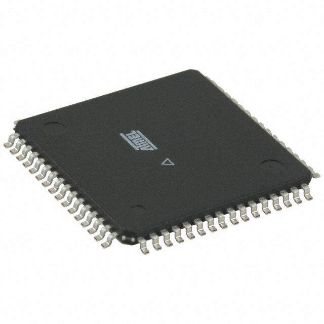
| 产品图片 |
|
| rohs | 符合RoHS无铅 / 符合限制有害物质指令(RoHS)规范要求 |
| 产品系列 | 嵌入式处理器和控制器,微控制器 - MCU,32位微控制器 - MCU,Texas Instruments TMS320F28022PTTC2000™ C28x Piccolo™ |
| 数据手册 | |
| 产品型号 | TMS320F28022PTT |
| PCN组件/产地 | |
| RAM容量 | 6K x 16 |
| 产品培训模块 | http://www.digikey.cn/PTM/IndividualPTM.page?site=cn&lang=zhs&ptm=21690http://www.digikey.cn/PTM/IndividualPTM.page?site=cn&lang=zhs&ptm=25065http://www.digikey.cn/PTM/IndividualPTM.page?site=cn&lang=zhs&ptm=25339http://www.digikey.cn/PTM/IndividualPTM.page?site=cn&lang=zhs&ptm=25870http://www.digikey.cn/PTM/IndividualPTM.page?site=cn&lang=zhs&ptm=26035http://www.digikey.cn/PTM/IndividualPTM.page?site=cn&lang=zhs&ptm=26105http://www.digikey.cn/PTM/IndividualPTM.page?site=cn&lang=zhs&ptm=30354 |
| 产品目录页面 | |
| 产品种类 | 32位微控制器 - MCU |
| 供应商器件封装 | 48-LQFP(7x7) |
| 其它名称 | 296-27541 |
| 制造商产品页 | http://www.ti.com/general/docs/suppproductinfo.tsp?distId=10&orderablePartNumber=TMS320F28022PTT |
| 包装 | 托盘 |
| 可编程输入/输出端数量 | 22 |
| 商标 | Texas Instruments |
| 商标名 | Piccolo |
| 处理器系列 | TMS320F2x |
| 外设 | 欠压检测/复位,POR,PWM,WDT |
| 安装风格 | SMD/SMT |
| 定时器数量 | 3 Timer |
| 封装/外壳 | 48-LQFP |
| 封装/箱体 | LQFP-48 |
| 工作温度 | -40°C ~ 105°C |
| 工作电源电压 | 3.3 V |
| 工厂包装数量 | 250 |
| 振荡器类型 | 内部 |
| 数据RAM大小 | 12 kB |
| 数据总线宽度 | 32 bit |
| 数据转换器 | A/D 13x12b |
| 最大工作温度 | + 105 C |
| 最大时钟频率 | 50 MHz |
| 最小工作温度 | - 40 C |
| 标准包装 | 250 |
| 核心 | C28x |
| 核心处理器 | C28x |
| 核心尺寸 | 32-位 |
| 片上ADC | Yes |
| 电压-电源(Vcc/Vdd) | 1.71 V ~ 1.995 V |
| 程序存储器大小 | 32 kB |
| 程序存储器类型 | 闪存 |
| 程序存储容量 | 32KB(16K x 16) |
| 系列 | TMS320F28022 |
| 输入/输出端数量 | 22 I/O |
| 连接性 | I²C, SCI, SPI, UART/USART |
| 速度 | 50MHz |


- 商务部:美国ITC正式对集成电路等产品启动337调查
- 曝三星4nm工艺存在良率问题 高通将骁龙8 Gen1或转产台积电
- 太阳诱电将投资9.5亿元在常州建新厂生产MLCC 预计2023年完工
- 英特尔发布欧洲新工厂建设计划 深化IDM 2.0 战略
- 台积电先进制程称霸业界 有大客户加持明年业绩稳了
- 达到5530亿美元!SIA预计今年全球半导体销售额将创下新高
- 英特尔拟将自动驾驶子公司Mobileye上市 估值或超500亿美元
- 三星加码芯片和SET,合并消费电子和移动部门,撤换高东真等 CEO
- 三星电子宣布重大人事变动 还合并消费电子和移动部门
- 海关总署:前11个月进口集成电路产品价值2.52万亿元 增长14.8%


PDF Datasheet 数据手册内容提取
Product Order Technical Tools & Support & Folder Now Documents Software Community TMS320F28027,TMS320F28026,TMS320F28023,TMS320F28022 TMS320F28021,TMS320F28020,TMS320F280200 SPRS523M–NOVEMBER2008–REVISEDJANUARY2019 TMS320F2802x Piccolo™ Microcontrollers 1 Device Overview 1.1 Features 1 • High-Efficiency32-BitCPU(TMS320C28x) • On-ChipMemory – 60MHz(16.67-nsCycleTime) – Flash,SARAM,OTP,BootROMAvailable – 50MHz(20-nsCycleTime) • Code-SecurityModule – 40MHz(25-nsCycleTime) • 128-BitSecurityKeyandLock – 16× 16and32×32MACOperations – ProtectsSecureMemoryBlocks – 16× 16DualMAC – PreventsFirmwareReverseEngineering – HarvardBusArchitecture • SerialPortPeripherals – AtomicOperations – OneSerialCommunicationsInterface(SCI) – FastInterruptResponseandProcessing UniversalAsynchronousReceiver/Transmitter (UART)Module – UnifiedMemoryProgrammingModel – OneSerialPeripheralInterface(SPI)Module – Code-Efficient(inC/C++andAssembly) – OneInter-Integrated-Circuit(I2C)Module • Endianness:LittleEndian • EnhancedControlPeripherals • LowCostforBothDeviceandSystem: – ePWM – Single3.3-VSupply – High-ResolutionPWM(HRPWM) – NoPowerSequencingRequirement – EnhancedCapture(eCAP)Module – IntegratedPower-onandBrown-outResets – Analog-to-DigitalConverter(ADC) – SmallPackaging,asLowas38-PinAvailable – On-ChipTemperatureSensor – LowPower – Comparator – NoAnalogSupportPins • AdvancedEmulationFeatures • Clocking: – AnalysisandBreakpointFunctions – TwoInternalZero-PinOscillators – Real-TimeDebugThroughHardware – On-ChipCrystalOscillatorandExternalClock Input • PackageOptions – WatchdogTimerModule – 38-PinDAThinShrinkSmall-OutlinePackage (TSSOP) – MissingClockDetectionCircuitry – 48-PinPTLow-ProfileQuadFlatpack(LQFP) • Upto22IndividuallyProgrammable,Multiplexed GPIOPinsWithInputFiltering • TemperatureOptions • PeripheralInterruptExpansion(PIE)BlockThat – T: –40°Cto105°C SupportsAllPeripheralInterrupts – S: –40°Cto125°C • Three32-BitCPUTimers – Q: –40°Cto125°C • Independent16-BitTimerinEachEnhancedPulse (AECQ100QualificationforAutomotive WidthModulator(ePWM) Applications) 1.2 Applications • Appliances • GridInfrastructure • BuildingAutomation • Medical,HealthcareandFitness • ElectricVehicle/HybridElectricVehicle(EV/HEV) • MotorDrives Powertrain • PowerDelivery • FactoryAutomation • TelecomInfrastructure 1 An IMPORTANT NOTICE at the end of this data sheet addresses availability, warranty, changes, use in safety-critical applications, intellectualpropertymattersandotherimportantdisclaimers.PRODUCTIONDATA.
TMS320F28027,TMS320F28026,TMS320F28023,TMS320F28022 TMS320F28021,TMS320F28020,TMS320F280200 SPRS523M–NOVEMBER2008–REVISEDJANUARY2019 www.ti.com 1.3 Description C2000™ 32-bit microcontrollers are optimized for processing, sensing, and actuation to improve closed- loop performance in real-time control applications such as industrial motor drives; solar inverters and digital power; electrical vehicles and transportation; motor control; and sensing and signal processing. The C2000 line includes the Delfino™ Premium Performance family and the Piccolo™ Entry Performance family. The F2802x Piccolo™ family of microcontrollers provides the power of the C28x core coupled with highly integrated control peripherals in low pin-count devices. This family is code-compatible with previous C28x- basedcode,andalsoprovidesahighlevelofanalogintegration. An internal voltage regulator allows for single-rail operation. Enhancements have been made to the HRPWM to allow for dual-edge control (frequency modulation). Analog comparators with internal 10-bit references have been added and can be routed directly to control the PWM outputs. The ADC converts from 0 to 3.3-V fixed full-scale range and supports ratio-metric V /V references. The ADC REFHI REFLO interfacehasbeenoptimizedforlowoverheadandlatency. TolearnmoreabouttheC2000MCUs,visittheC2000Overviewat www.ti.com/c2000. DeviceInformation(1) PARTNUMBER PACKAGE BODYSIZE TMS320F28027PT LQFP(48) 7.0mm×7.0mm TMS320F28026PT LQFP(48) 7.0mm×7.0mm TMS320F28023PT LQFP(48) 7.0mm×7.0mm TMS320F28022PT LQFP(48) 7.0mm×7.0mm TMS320F28021PT LQFP(48) 7.0mm×7.0mm TMS320F28020PT LQFP(48) 7.0mm×7.0mm TMS320F280200PT LQFP(48) 7.0mm×7.0mm TMS320F28027DA TSSOP(38) 12.5mm×6.2mm TMS320F28026DA TSSOP(38) 12.5mm×6.2mm TMS320F28023DA TSSOP(38) 12.5mm×6.2mm TMS320F28022DA TSSOP(38) 12.5mm×6.2mm TMS320F28021DA TSSOP(38) 12.5mm×6.2mm TMS320F28020DA TSSOP(38) 12.5mm×6.2mm TMS320F280200DA TSSOP(38) 12.5mm×6.2mm (1) Formoreinformationonthesedevices,seeMechanical,Packaging,andOrderableInformation. 2 DeviceOverview Copyright©2008–2019,TexasInstrumentsIncorporated SubmitDocumentationFeedback ProductFolderLinks:TMS320F28027TMS320F28026 TMS320F28023 TMS320F28022 TMS320F28021 TMS320F28020 TMS320F280200
TMS320F28027,TMS320F28026,TMS320F28023,TMS320F28022 TMS320F28021,TMS320F28020,TMS320F280200 www.ti.com SPRS523M–NOVEMBER2008–REVISEDJANUARY2019 1.4 Functional Block Diagram FunctionalBlockDiagramshowsthefunctionalblockdiagramforthedevice. us OTP1K × 16 B Secure M0 ory SARAM 1K × 16 m (0-wait) Me M1 SARAM SARAM 1K × 16 1K/3K/4K × 16 Code FLASH (0-wait) (0-wait) Security 8K/16K/32K × 16 Secure Module Secure Boot-ROM 8K × 16 (0-wait) OTP/Flash PSWD Wrapper Memory Bus TRST TCK COMP1OUT GPIO COMP2OUT us C28x TTMDSI MUX al B 32-Bit CPU TDO GPIO er Mux COMP1A h CCOOMMPP12BA COMP Perip COMP2B Bit PIE 3 External Interrupts 2- 3 CPU Timer 0 OSC1, XCLKIN OSC2, X1 AIO Ext, X2 MUX CPU Timer 1 PLL, LPM Wakeup LPM, XRS CPU Timer 2 WD ADC A7:0 Memory Bus POR/ VREG B7:0 BOR 16-Bit Peripheral Bus 32-Bit Peripheral Bus 32-Bit Peripheral Bus SCI SPI I2C ePWM eCAP (4LFIFO) (4LFIFO) (4LFIFO) HRPWM O SCITXDx SCIRXDx SPISIMOx SPISOMIx SPICLKx SPISTEx SDAx SCLx TZx EPWMxA EPWMxB PWMSYNCI EPWMSYNCCCOOMMFrPPo12mOOUUTT, ECAPx E GPIO MUX Copyright © 2017,Texas Instruments Incorporated A. Notallperipheralpinsareavailableatthesametimeduetomultiplexing. Figure1-1.FunctionalBlockDiagram Copyright©2008–2019,TexasInstrumentsIncorporated DeviceOverview 3 SubmitDocumentationFeedback ProductFolderLinks:TMS320F28027TMS320F28026 TMS320F28023 TMS320F28022 TMS320F28021 TMS320F28020 TMS320F280200
TMS320F28027,TMS320F28026,TMS320F28023,TMS320F28022 TMS320F28021,TMS320F28020,TMS320F280200 SPRS523M–NOVEMBER2008–REVISEDJANUARY2019 www.ti.com Table of Contents 1 DeviceOverview......................................... 1 5.14 FlashTiming........................................ 34 1.1 Features.............................................. 1 6 DetailedDescription................................... 37 ........................................... ............................................ 1.2 Applications 1 6.1 Overview 37 ............................................ ...................................... 1.3 Description 2 6.2 MemoryMaps 45 ........................... ....................................... 1.4 FunctionalBlockDiagram 3 6.3 Register Maps 53 2 Revision History......................................... 5 6.4 DeviceEmulationRegisters......................... 54 3 DeviceComparison ..................................... 6 6.5 VREG/BOR/POR.................................... 55 ..................................... ...................................... 3.1 RelatedProducts 8 6.6 SystemControl 57 4 TerminalConfigurationandFunctions.............. 9 6.7 Low-powerModesBlock............................ 65 ......................................... ............................................ 4.1 PinDiagrams 9 6.8 Interrupts 66 .................................. .......................................... 4.2 SignalDescriptions 11 6.9 Peripherals 71 5 Specifications........................................... 16 7 Applications,Implementation,andLayout...... 122 ........................ .................... 5.1 AbsoluteMaximumRatings 16 7.1 TIDesignorReferenceDesign 122 5.2 ESDRatings–Automotive.......................... 16 8 DeviceandDocumentationSupport.............. 123 ......................... ..................................... 5.3 ESDRatings–Commercial 17 8.1 Getting Started 123 5.4 RecommendedOperatingConditions............... 17 8.2 DeviceandDevelopmentSupportTool ...................................... ...................... Nomenclature 123 5.5 PowerConsumptionSummary 18 ................................ ............................ 8.3 ToolsandSoftware 124 5.6 ElectricalCharacteristics 23 ............................ ................ 8.4 DocumentationSupport 126 5.7 ThermalResistanceCharacteristics 24 ...................................... .................... 8.5 RelatedLinks 127 5.8 ThermalDesignConsiderations 25 ............................. 5.9 EmulatorConnectionWithoutSignalBufferingfor 8.6 CommunityResources 127 ............................................. ........................................ theMCU 25 8.7 Trademarks 127 .............................. ................... 5.10 ParameterInformation 26 8.8 ElectrostaticDischargeCaution 127 ................................... ............................................ 5.11 TestLoadCircuit 26 8.9 Glossary 127 5.12 PowerSequencing.................................. 27 9 Mechanical,Packaging,andOrderable ................................. Information............................................. 128 5.13 ClockSpecifications 30 ............................. 9.1 PackagingInformation 128 4 TableofContents Copyright©2008–2019,TexasInstrumentsIncorporated SubmitDocumentationFeedback ProductFolderLinks:TMS320F28027TMS320F28026 TMS320F28023 TMS320F28022 TMS320F28021 TMS320F28020 TMS320F280200
TMS320F28027,TMS320F28026,TMS320F28023,TMS320F28022 TMS320F28021,TMS320F28020,TMS320F280200 www.ti.com SPRS523M–NOVEMBER2008–REVISEDJANUARY2019 2 Revision History ChangesfromDecember15,2017toJanuary8,2019(fromLRevision(December2017)toMRevision) Page • Global:ReplacedindividualperipheralguideswiththeTMS320F2802x,TMS320F2802xxPiccoloTechnical ReferenceManual.................................................................................................................... 1 • Section1.3(Description):Updatedsection. ...................................................................................... 2 • Section3.1(RelatedProducts):Updatedsection. ............................................................................... 8 • Table4-1(SignalDescriptions):UpdatedDESCRIPTIONofXRS........................................................... 11 • Table5-11(InternalZero-PinOscillator(INTOSC1/INTOSC2)Characteristics):Updated"Oscillatorfrequency willvaryovertemperature..."footnote:ReplacedthecontrolSUITEexamplewithC2000Ware......................... 32 • Section6.1.8(BootROM):Updated"TheBootROMisfactory-programmed..."paragraph............................. 39 • Figure6-13(ExternalandPIEInterruptSources):Updatedfigure........................................................... 66 • Section8.3(ToolsandSoftware):Added"C2000WareforC2000MCUs"and"UniFlashStandaloneFlashTool".. 124 • Section8.4(DocumentationSupport):Replacedindividualperipheralguideswiththe TMS320F2802x,TMS320F2802xxPiccoloTechnicalReferenceManual.Updatedsection............................. 126 Copyright©2008–2019,TexasInstrumentsIncorporated RevisionHistory 5 SubmitDocumentationFeedback ProductFolderLinks:TMS320F28027TMS320F28026 TMS320F28023 TMS320F28022 TMS320F28021 TMS320F28020 TMS320F280200
TMS320F28027,TMS320F28026,TMS320F28023,TMS320F28022 TMS320F28021,TMS320F28020,TMS320F280200 SPRS523M–NOVEMBER2008–REVISEDJANUARY2019 www.ti.com 3 Device Comparison Table3-1liststhefeaturesoftheTMS320F2802xdevices. Table3-1.DeviceComparison 28027 28026 FEATURE TYPE(1) 28027F(2) 28026F(2) 28023 28022 28021 28020 280200 (50MHz) (50MHz) (40MHz) (40MHz) (40MHz) (60MHz) (60MHz) 38-PinDA 48-PinPT 38-PinDA 48-PinPT 38-PinDA 48-PinPT 38-PinDA 48-PinPT 38-PinDA 48-PinPT 38-PinDA 48-PinPT 38-PinDA 48-PinPT PackageType TSSOP LQFP TSSOP LQFP TSSOP LQFP TSSOP LQFP TSSOP LQFP TSSOP LQFP TSSOP LQFP Instructioncycle – 16.67ns 16.67ns 20ns 20ns 25ns 25ns 25ns On-chipflash(16-bitword) – 32K 16K 32K 16K 32K 16K 8K On-chipSARAM(16-bitword) – 6K 6K 6K 6K 5K 3K 3K Codesecurityforon-chip – Yes Yes Yes Yes Yes Yes Yes flash/SARAM/OTPblocks BootROM(8Kx16) – Yes Yes Yes Yes Yes Yes Yes One-timeprogrammable(OTP)ROM(16- – 1K 1K 1K 1K 1K 1K 1K bitword) ePWMchannels 1 8(ePWM1/2/3/4) 8(ePWM1/2/3/4) 8(ePWM1/2/3/4) 8(ePWM1/2/3/4) 8(ePWM1/2/3/4) 8(ePWM1/2/3/4) 8(ePWM1/2/3/4) eCAPinputs 0 1 1 1 1 1 1 – Watchdogtimer – Yes Yes Yes Yes Yes Yes Yes MSPS 4.6 4.6 3 3 2 2 2 ConversionTime 216.67ns 216.67ns 260ns 260ns 500ns 500ns 500ns 12-BitADC Channels 3 7 13 7 13 7 13 7 13 7 13 7 13 7 13 TemperatureSensor Yes Yes Yes Yes Yes Yes Yes DualSample-and-Hold Yes Yes Yes Yes Yes Yes Yes 32-BitCPUtimers – 3 3 3 3 3 3 3 High-resolutionePWMChannels 1 4(ePWM1A/2A/3A/4A) 4(ePWM1A/2A/3A/4A) 4(ePWM1A/2A/3A/4A) 4(ePWM1A/2A/3A/4A) – – – Comparatorsw/IntegratedDACs 0 1 2 1 2 1 2 1 2 1 2 1 2 1 2 Inter-integratedcircuit(I2C) 0 1 1 1 1 1 1 1 SerialPeripheralInterface(SPI) 1 1 1 1 1 1 1 1 SerialCommunicationsInterface(SCI) 0 1 1 1 1 1 1 1 Digital(GPIO) – 20 22 20 22 20 22 20 22 20 22 20 22 20 22 I/Opins(shared) Analog(AIO) – 6 6 6 6 6 6 6 Externalinterrupts – 3 3 3 3 3 3 3 Supplyvoltage(nominal) – 3.3V 3.3V 3.3V 3.3V 3.3V 3.3V 3.3V (1) Atypechangerepresentsamajorfunctionalfeaturedifferenceinaperipheralmodule.Withinaperipheraltype,theremaybeminordifferencesbetweendevicesthatdonotaffectthe basicfunctionalityofthemodule.Thesedevice-specificdifferencesarelistedintheC2000Real-TimeControlPeripheralsReferenceGuideandintheTMS320F2802x,TMS320F2802xx PiccoloTechnicalReferenceManual. (2) TMS320F28027FandTMS320F28026FareInstaSPIN-FOC™-enabledMCUs.Formoreinformation,seeSection8.4foralistofInstaSPINTechnicalReferenceManuals. 6 DeviceComparison Copyright©2008–2019,TexasInstrumentsIncorporated SubmitDocumentationFeedback ProductFolderLinks:TMS320F28027TMS320F28026 TMS320F28023 TMS320F28022 TMS320F28021 TMS320F28020 TMS320F280200
TMS320F28027,TMS320F28026,TMS320F28023,TMS320F28022 TMS320F28021,TMS320F28020,TMS320F280200 www.ti.com SPRS523M–NOVEMBER2008–REVISEDJANUARY2019 Table3-1.DeviceComparison(continued) 28027 28026 FEATURE TYPE(1) 28027F(2) 28026F(2) 28023 28022 28021 28020 280200 (50MHz) (50MHz) (40MHz) (40MHz) (40MHz) (60MHz) (60MHz) 38-PinDA 48-PinPT 38-PinDA 48-PinPT 38-PinDA 48-PinPT 38-PinDA 48-PinPT 38-PinDA 48-PinPT 38-PinDA 48-PinPT 38-PinDA 48-PinPT PackageType TSSOP LQFP TSSOP LQFP TSSOP LQFP TSSOP LQFP TSSOP LQFP TSSOP LQFP TSSOP LQFP T:–40°Cto105°C – Yes Yes Yes Yes Yes Yes Yes Yes Yes Yes Yes Yes Yes Yes Temperature S:–40°Cto125°C – Yes Yes Yes Yes Yes Yes Yes Yes Yes Yes Yes Yes Yes Yes options Q:–40°Cto125°C(3) – Yes Yes Yes Yes Yes Yes Yes Yes – – – – – – (3) TheletterQreferstoAECQ100qualificationforautomotiveapplications. Copyright©2008–2019,TexasInstrumentsIncorporated DeviceComparison 7 SubmitDocumentationFeedback ProductFolderLinks:TMS320F28027TMS320F28026 TMS320F28023 TMS320F28022 TMS320F28021 TMS320F28020 TMS320F280200
TMS320F28027,TMS320F28026,TMS320F28023,TMS320F28022 TMS320F28021,TMS320F28020,TMS320F280200 SPRS523M–NOVEMBER2008–REVISEDJANUARY2019 www.ti.com 3.1 Related Products Forinformationaboutotherdevicesinthe Piccolofamilyofproducts,seethefollowinglinks: OriginalPiccolo™series: TMS320F2802xPiccolo™Microcontrollers The F2802x series is the original Piccolo and offers the lowest pin-count and Flash memory size options. InstaSPIN-FOC™versionsareavailable. TMS320F2803xPiccolo™Microcontrollers The F2803x series increases the pin-count and memory size options. The F2803x series also introduces theparallelcontrollawaccelerator(CLA)option. TMS320F2805xPiccolo™Microcontrollers The F2805x series is similar to the F2803x series but adds on-chip programmable gain amplifiers (PGAs). InstaSPIN-FOCand InstaSPIN-MOTION™versionsareavailable. TMS320F2806xPiccolo™Microcontrollers The F2806x series is the first to include a floating-point unit (FPU). The F2806x series also increases the pin-count, memory size options, and the quantity of peripherals. InstaSPIN-FOC™ and InstaSPIN- MOTION™versionsareavailable. NewestPiccolo™series: TMS320F2807xPiccolo™Microcontrollers TheF2807xseriesisthehighest-endPiccolowiththemostperformance,largestpincounts,flashmemory sizes, and peripheral options. The F2807x series includes the latest generation of accelerators, ePWM peripherals,andanalogtechnology. TMS320F28004xPiccolo™Microcontrollers The F28004x series is a reduced version of the F2807x series with the latest generational enhancements. The F28004x series is the best roadmap option for those using the F2806x series. InstaSPIN-FOC and configurablelogicblock(CLB)versionsareavailable. 8 DeviceComparison Copyright©2008–2019,TexasInstrumentsIncorporated SubmitDocumentationFeedback ProductFolderLinks:TMS320F28027TMS320F28026 TMS320F28023 TMS320F28022 TMS320F28021 TMS320F28020 TMS320F280200
TMS320F28027,TMS320F28026,TMS320F28023,TMS320F28022 TMS320F28021,TMS320F28020,TMS320F280200 www.ti.com SPRS523M–NOVEMBER2008–REVISEDJANUARY2019 4 Terminal Configuration and Functions 4.1 Pin Diagrams Figure 4-1 shows the 48-pin PT low-profile quad flatpack (LQFP) pin assignments. Figure 4-2 shows the 38-pinDAthinshrinksmall-outlinepackage(TSSOP)pinassignments. 1 P O O A B A C C C E O O A/ DCS DCS RXD NCO/A NCI/A OUT /ASCI GPIO33/SCLA/EPWMSYVDDIOVREGENZ VSSVDDGPIO32/SDAA/EPWMSYTESTGPIO0/EPWM1AGPIO1/EPWM1B/COMP1GPIO16/SPISIMOA/TZ2GPIO17/SPISOMIA/TZ3GPIO19/XCLKIN/SPISTE 654321098765 333333322222 GPIO2/EPWM2A 37 24 GPIO18/SPICLKA/SCITXDA/XCLKOUT GPIO3/EPWM2B/COMP2OUT 38 23 GPIO38/XCLKIN (TCK) GPIO4/EPWM3A 39 22 GPIO37 (TDO) GPIO5/EPWM3B/ECAP1 40 21 GPIO36 (TMS) GPIO6/EPWM4A/EPWMSYNCI/EPWMSYNCO 41 20 GPIO35 (TDI) GPIO7/EPWM4B/SCIRXDA 42 19 GPIO34/COMP2OUT VDD 43 18 ADCINB7 VSS 44 17 ADCINB6/AIO14 X1 45 16 ADCINB4/COMP2B/AIO12 X2 46 15 ADCINB3 GPIO12/TZ1/SCITXDA 47 14 ADCINB2/COMP1B/AIO10 GPIO28/SCIRXDA/SDAA/TZ2 48 13 ADCINB1 012 123456789111 DA/SCLA/TZ3 TRST XRSDCINA6/AIO6OMP2A/AIO4ADCINA7ADCINA3ADCINA1OMP1A/AIO2CINA0/VREFHIVDDA/VVSSAREFLO X AC CD T 4/ 2/A CI A A S N N 9/ CI CI 2 D D O A A PI G Figure4-1.2802x48-PinPTLQFP(TopView) Copyright©2008–2019,TexasInstrumentsIncorporated TerminalConfigurationandFunctions 9 SubmitDocumentationFeedback ProductFolderLinks:TMS320F28027TMS320F28026 TMS320F28023 TMS320F28022 TMS320F28021 TMS320F28020 TMS320F280200
TMS320F28027,TMS320F28026,TMS320F28023,TMS320F28022 TMS320F28021,TMS320F28020,TMS320F280200 SPRS523M–NOVEMBER2008–REVISEDJANUARY2019 www.ti.com VDD 1 38 TEST VSS 2 37 GPIO0/EPWM1A VREGENZ 3 36 GPIO1/EPWM1B/COMP1OUT VDDIO 4 35 GPIO16/SPISIMOA/TZ2 GPIO2/EPWM2A 5 34 GPIO17/SPISOMIA/TZ3 GPIO3/EPWM2B 6 33 GPIO19/XCLKIN/SPISTEA/SCIRXDA/ECAP1 GPIO4/EPWM3A 7 32 GPIO18/SPICLKA/SCITXDA/XCLKOUT GPIO5/EPWM3B/ECAP1 8 31 GPIO38/XCLKIN (TCK) GPIO6/EPWM4A/EPWMSYNCI/EPWMSYNCO 9 30 GPIO37 (TDO) GPIO7/EPWM4B/SCIRXDA 10 29 GPIO36 (TMS) VDD 11 28 GPIO35 (TDI) VSS 12 27 GPIO34 GPIO12/TZ1/SCITXDA 13 26 ADCINB6/AIO14 GPIO28/SCIRXDA/SDAA/TZ2 14 25 ADCINB4/AIO12 GPIO29/SCITXDA/SCLA/TZ3 15 24 ADCINB2/COMP1B/AIO10 TRST 16 23 VSSA/VREFLO XRS 17 22 VDDA ADCINA6/AIO6 18 21 ADCINA0/V REFHI ADCINA4/AIO4 19 20 ADCINA2/COMP1A/AIO2 Figure4-2.2802x38-PinDATSSOP(TopView) 10 TerminalConfigurationandFunctions Copyright©2008–2019,TexasInstrumentsIncorporated SubmitDocumentationFeedback ProductFolderLinks:TMS320F28027TMS320F28026 TMS320F28023 TMS320F28022 TMS320F28021 TMS320F28020 TMS320F280200
TMS320F28027,TMS320F28026,TMS320F28023,TMS320F28022 TMS320F28021,TMS320F28020,TMS320F280200 www.ti.com SPRS523M–NOVEMBER2008–REVISEDJANUARY2019 4.2 Signal Descriptions Table 4-1 describes the signals. With the exception of the JTAG pins, the GPIO function is the default at reset, unless otherwise mentioned. The peripheral signals that are listed under them are alternate functions. Some peripheral functions may not be available in all devices. See Table 3-1 for details. Inputs are not 5-V tolerant. All GPIO pins are I/O/Z and have an internal pullup, which can be selectively enabled/disabled on a per-pin basis. This feature only applies to the GPIO pins. The pullups on the PWM pins are not enabled at reset. The pullups on other GPIO pins are enabled upon reset. The AIO pins do nothaveaninternalpullup. NOTE When the on-chip VREG is used, the GPIO19, GPIO34, GPIO35, GPIO36, GPIO37, and GPIO38 pins could glitch during power up. This potential glitch will finish before the boot mode pins are read and will not affect boot behavior. If glitching is unacceptable in an application,1.8Vcouldbesuppliedexternally.Alternatively,addingacurrent-limitingresistor (forexample,470Ω)inserieswiththesepinsandanyexternaldrivercouldbeconsideredto limit the potential for degradation to the pin and/or external circuitry. There is no power- sequencing requirement when using an external 1.8-V supply. However, if the 3.3-V transistors in the level-shifting output buffers of the I/O pins are powered before the 1.8-V transistors,itispossiblefortheoutputbufferstoturnon,causingaglitchtooccuronthepin during power up. To avoid this behavior, power the V pins before or with the V pins, DD DDIO ensuringthattheV pinshavereached0.7VbeforetheV pinsreach0.7V. DD DDIO Table4-1. SignalDescriptions(1) TERMINAL PT DA I/O/Z DESCRIPTION NAME PINNO. PINNO. JTAG JTAGtestresetwithinternalpulldown.TRST,whendrivenhigh,givesthescan systemcontroloftheoperationsofthedevice.Ifthissignalisnotconnectedor drivenlow,thedeviceoperatesinitsfunctionalmode,andthetestresetsignals areignored. NOTE:TRSTisanactivehightestpinandmustbemaintainedlowatalltimes TRST 2 16 I duringnormaldeviceoperation.Anexternalpulldownresistorisrequiredonthis pin.Thevalueofthisresistorshouldbebasedondrivestrengthofthedebugger podsapplicabletothedesign.A2.2-kΩresistorgenerallyoffersadequate protection.Becausethisisapplication-specific,TIrecommendsvalidatingeach targetboardforproperoperationofthedebuggerandtheapplication.(↓) TCK SeeGPIO38 I SeeGPIO38.JTAGtestclockwithinternalpullup(↑) SeeGPIO36.JTAGtest-modeselect(TMS)withinternalpullup.Thisserialcontrol TMS SeeGPIO36 I inputisclockedintotheTAPcontrollerontherisingedgeofTCK.(↑) SeeGPIO35.JTAGtestdatainput(TDI)withinternalpullup.TDIisclockedinto TDI SeeGPIO35 I theselectedregister(instructionordata)onarisingedgeofTCK.(↑) SeeGPIO37.JTAGscanout,testdataoutput(TDO).Thecontentsofthe selectedregister(instructionordata)areshiftedoutofTDOonthefallingedgeof TDO SeeGPIO37 O/Z TCK. (8-mAdrive) FLASH TEST 30 38 I/O TestPin.ReservedforTI.Mustbeleftunconnected. (1) I=Input,O=Output,Z=HighImpedance,OD=OpenDrain,↑=Pullup,↓=Pulldown Copyright©2008–2019,TexasInstrumentsIncorporated TerminalConfigurationandFunctions 11 SubmitDocumentationFeedback ProductFolderLinks:TMS320F28027TMS320F28026 TMS320F28023 TMS320F28022 TMS320F28021 TMS320F28020 TMS320F280200
TMS320F28027,TMS320F28026,TMS320F28023,TMS320F28022 TMS320F28021,TMS320F28020,TMS320F280200 SPRS523M–NOVEMBER2008–REVISEDJANUARY2019 www.ti.com Table4-1. SignalDescriptions(1) (continued) TERMINAL PT DA I/O/Z DESCRIPTION NAME PINNO. PINNO. CLOCK SeeGPIO18.OutputclockderivedfromSYSCLKOUT.XCLKOUTiseitherthe samefrequency,one-halfthefrequency,orone-fourththefrequencyof SYSCLKOUT.Thisiscontrolledbybits1:0(XCLKOUTDIV)intheXCLKregister. XCLKOUT SeeGPIO18 O/Z Atreset,XCLKOUT=SYSCLKOUT/4.TheXCLKOUTsignalcanbeturnedoffby settingXCLKOUTDIVto3.ThemuxcontrolforGPIO18mustalsobesetto XCLKOUTforthissignaltopropogatetothepin. SeeGPIO19andGPIO38.Externaloscillatorinput.Pinsourcefortheclockis controlledbytheXCLKINSELbitintheXCLKregister,GPIO38isthedefault selection.Thispinfeedsaclockfromanexternal3.3-Voscillator.Inthiscase,the X1pin,ifavailable,mustbetiedtoGNDandtheon-chipcrystaloscillatormustbe disabledthroughbit14intheCLKCTLregister.Ifacrystal/resonatorisused,the XCLKIN SeeGPIO19andGPIO38 I XCLKINpathmustbedisabledbybit13intheCLKCTLregister. NOTE:DesignsthatusetheGPIO38/TCK/XCLKINpintosupplyanexternalclock fornormaldeviceoperationmayneedtoincorporatesomehookstodisablethis pathduringdebugusingtheJTAGconnector.Thisistopreventcontentionwith theTCKsignal,whichisactiveduringJTAGdebugsessions.Thezero-pininternal oscillatorsmaybeusedduringthistimetoclockthedevice. On-chip1.8-Vcrystal-oscillatorinput.Tousethisoscillator,aquartzcrystalora ceramicresonatormustbeconnectedacrossX1andX2.Inthiscase,theXCLKIN X1 45 – I pathmustbedisabledbybit13intheCLKCTLregister.Ifthispinisnotused,it mustbetiedtoGND.(I) On-chipcrystal-oscillatoroutput.Aquartzcrystaloraceramicresonatormustbe X2 46 – O connectedacrossX1andX2.IfX2isnotused,itmustbeleftunconnected.(O) RESET DeviceReset(in)andWatchdogReset(out).Piccolodeviceshaveabuilt-in power-onreset(POR)andbrown-outreset(BOR)circuitry.Duringapower-onor brown-outcondition,thispinisdrivenlowbythedevice.Anexternalcircuitmay alsodrivethispintoassertadevicereset.ThispinisalsodrivenlowbytheMCU whenawatchdogresetoccurs.Duringwatchdogreset,theXRSpinisdrivenlow forthewatchdogresetdurationof512OSCCLKcycles.Aresistorwithavalue from2.2kΩto10kΩshouldbeplacedbetweenXRSandV .Ifacapacitoris DDIO placedbetweenXRSandV fornoisefiltering,itshouldbe100nForsmaller. XRS 3 17 I/OD SS ThesevalueswillallowthewatchdogtoproperlydrivetheXRSpintoV within OL 512OSCCLKcycleswhenthewatchdogresetisasserted.Regardlessofthe source,adeviceresetcausesthedevicetoterminateexecution.Theprogram counterpointstotheaddresscontainedatthelocation0x3FFFC0.Whenresetis deactivated,executionbeginsatthelocationdesignatedbytheprogramcounter. Theoutputbufferofthispinisanopen-draindevicewithaninternalpullup.(↑)If thispinisdrivenbyanexternaldevice,itshouldbedoneusinganopen-drain device. ADC,COMPARATOR,ANALOGI/O ADCINA7 6 – I ADCGroupA,Channel7input ADCINA6 I ADCGroupA,Channel6input 4 18 AIO6 I/O DigitalAIO6 ADCINA4 I ADCGroupA,Channel4input COMP2A 5 19 I ComparatorInput2A(availablein48-pindeviceonly) AIO4 I/O DigitalAIO4 ADCINA3 7 – I ADCGroupA,Channel3input ADCINA2 I ADCGroupA,Channel2input COMP1A 9 20 I ComparatorInput1A AIO2 I/O DigitalAIO2 ADCINA1 8 – I ADCGroupA,Channel1input ADCINA0 I ADCGroupA,Channel0input V 10 21 I ADCExternalReferenceHigh–onlyusedwheninADCexternalreferencemode. REFHI SeeSection6.9.1.1,ADC. ADCINB7 18 – I ADCGroupB,Channel7input 12 TerminalConfigurationandFunctions Copyright©2008–2019,TexasInstrumentsIncorporated SubmitDocumentationFeedback ProductFolderLinks:TMS320F28027TMS320F28026 TMS320F28023 TMS320F28022 TMS320F28021 TMS320F28020 TMS320F280200
TMS320F28027,TMS320F28026,TMS320F28023,TMS320F28022 TMS320F28021,TMS320F28020,TMS320F280200 www.ti.com SPRS523M–NOVEMBER2008–REVISEDJANUARY2019 Table4-1. SignalDescriptions(1) (continued) TERMINAL PT DA I/O/Z DESCRIPTION NAME PINNO. PINNO. ADCINB6 I ADCGroupB,Channel6input 17 26 AIO14 I/O DigitalAIO14 ADCINB4 I ADCGroupB,Channel4input COMP2B 16 25 I ComparatorInput2B(availablein48-pindeviceonly) AIO12 I/O DigitalAIO12 ADCINB3 15 – I ADCGroupB,Channel3input ADCINB2 I ADCGroupB,Channel2input COMP1B 14 24 I ComparatorInput1B AIO10 I/O DigitalAIO10 ADCINB1 13 – I ADCGroupB,Channel1input CPUANDI/OPOWER V 11 22 AnalogPowerPin.Tiewitha2.2-µFcapacitor(typical)closetothepin. DDA V AnalogGroundPin SSA 12 23 V I ADCExternalReferenceLow(alwaystiedtoground) REFLO 32 1 CPUandLogicDigitalPowerPins.WhenusinginternalVREG,placeone1.2-µF V capacitorbetweeneachV pinandground.Highervaluecapacitorsmaybe DD DD 43 11 used. DigitalI/OBuffersandFlashMemoryPowerPin.Singlesupplysourcewhen V 35 4 VREGisenabled.Placeadecouplingcapacitoronthispin.Theexactvalue DDIO shouldbedeterminedbythesystemvoltageregulationsolution. 33 2 V DigitalGroundPins SS 44 12 VOLTAGEREGULATORCONTROLSIGNAL InternalVREGEnable/Disable.Pulllowtoenabletheinternalvoltageregulator VREGENZ 34 3 I (VREG),pullhightodisableVREG. GPIOANDPERIPHERALSIGNALS(2) GPIO0 I/O/Z General-purposeinput/output0 EPWM1A O EnhancedPWM1OutputAandHRPWMchannel 29 37 – – – – – – GPIO1 I/O/Z General-purposeinput/output1 EPWM1B O EnhancedPWM1OutputB 28 36 – – COMP1OUT O DirectoutputofComparator1 GPIO2 I/O/Z General-purposeinput/output2 EPWM2A O EnhancedPWM2OutputAandHRPWMchannel 37 5 – – – – GPIO3 I/O/Z General-purposeinput/output3 EPWM2B O EnhancedPWM2OutputB 38 6 – – COMP2OUT O DirectoutputofComparator2(availablein48-pindeviceonly) (2) TheGPIOfunction(showninbolditalics)isthedefaultatreset.Theperipheralsignalsthatarelistedunderthemarealternatefunctions. ForJTAGpinsthathavetheGPIOfunctionalitymultiplexed,theinputpathtotheGPIOblockisalwaysvalid.Theoutputpathfromthe GPIOblockandthepathtotheJTAGblockfromapinisenabled/disabledbasedontheconditionoftheTRSTsignal.SeetheSystem ControlchapterintheTMS320F2802x,TMS320F2802xxPiccoloTechnicalReferenceManualfordetails. Copyright©2008–2019,TexasInstrumentsIncorporated TerminalConfigurationandFunctions 13 SubmitDocumentationFeedback ProductFolderLinks:TMS320F28027TMS320F28026 TMS320F28023 TMS320F28022 TMS320F28021 TMS320F28020 TMS320F280200
TMS320F28027,TMS320F28026,TMS320F28023,TMS320F28022 TMS320F28021,TMS320F28020,TMS320F280200 SPRS523M–NOVEMBER2008–REVISEDJANUARY2019 www.ti.com Table4-1. SignalDescriptions(1) (continued) TERMINAL PT DA I/O/Z DESCRIPTION NAME PINNO. PINNO. GPIO4 I/O/Z General-purposeinput/output4 EPWM3A O EnhancedPWM3outputAandHRPWMchannel 39 7 – – – – GPIO5 I/O/Z General-purposeinput/output5 EPWM3B O EnhancedPWM3outputB 40 8 – – ECAP1 I/O EnhancedCaptureinput/output1 GPIO6 I/O/Z General-purposeinput/output6 EPWM4A O EnhancedPWM4outputAandHRPWMchannel 41 9 EPWMSYNCI I ExternalePWMsyncpulseinput EPWMSYNCO O ExternalePWMsyncpulseoutput GPIO7 I/O/Z General-purposeinput/output7 EPWM4B O EnhancedPWM4outputB 42 10 SCIRXDA I SCI-Areceivedata – – GPIO12 I/O/Z General-purposeinput/output12 TZ1 I TripZoneinput1 47 13 SCITXDA O SCI-Atransmitdata – – GPIO16 I/O/Z General-purposeinput/output16 SPISIMOA I/O SPIslavein,masterout 27 35 – – TZ2 I TripZoneinput2 GPIO17 I/O/Z General-purposeinput/output17 SPISOMIA I/O SPI-Aslaveout,masterin 26 34 – – TZ3 I Tripzoneinput3 GPIO18 I/O/Z General-purposeinput/output18 SPICLKA I/O SPI-Aclockinput/output SCITXDA O SCI-Atransmit XCLKOUT 24 32 O/Z OutputclockderivedfromSYSCLKOUT.XCLKOUTiseitherthesamefrequency, one-halfthefrequency,orone-fourththefrequencyofSYSCLKOUT.Thisis controlledbybits1:0(XCLKOUTDIV)intheXCLKregister.Atreset,XCLKOUT= SYSCLKOUT/4.TheXCLKOUTsignalcanbeturnedoffbysettingXCLKOUTDIV to3.ThemuxcontrolforGPIO18mustalsobesettoXCLKOUTforthissignalto propogatetothepin. GPIO19 I/O/Z General-purposeinput/output19 XCLKIN I ExternalOscillatorInput.Thepathfromthispintotheclockblockisnotgatedby themuxfunctionofthispin.Caremustbetakennottoenablethispathfor clockingifitisbeingusedfortheotherperiperhalfunctions 25 33 SPISTEA I/O SPI-Aslavetransmitenableinput/output SCIRXDA I SCI-Areceive ECAP1 I/O EnhancedCaptureinput/output1 GPIO28 I/O/Z General-purposeinput/output28 SCIRXDA I SCIreceivedata 48 14 SDAA I/OD I2Cdataopen-drainbidirectionalport TZ2 I Tripzoneinput2 14 TerminalConfigurationandFunctions Copyright©2008–2019,TexasInstrumentsIncorporated SubmitDocumentationFeedback ProductFolderLinks:TMS320F28027TMS320F28026 TMS320F28023 TMS320F28022 TMS320F28021 TMS320F28020 TMS320F280200
TMS320F28027,TMS320F28026,TMS320F28023,TMS320F28022 TMS320F28021,TMS320F28020,TMS320F280200 www.ti.com SPRS523M–NOVEMBER2008–REVISEDJANUARY2019 Table4-1. SignalDescriptions(1) (continued) TERMINAL PT DA I/O/Z DESCRIPTION NAME PINNO. PINNO. GPIO29 I/O/Z General-purposeinput/output29. SCITXDA O SCItransmitdata 1 15 SCLA I/OD I2Cclockopen-drainbidirectionalport TZ3 I Tripzoneinput3 GPIO32 I/O/Z General-purposeinput/output32 SDAA I/OD I2Cdataopen-drainbidirectionalport 31 – EPWMSYNCI I EnhancedPWMexternalsyncpulseinput ADCSOCAO O ADCstart-of-conversionA GPIO33 I/O/Z General-PurposeInput/Output33 SCLA I/OD I2Cclockopen-drainbidirectionalport 36 – EPWMSYNCO O EnhancedPWMexternalsynchpulseoutput ADCSOCBO O ADCstart-of-conversionB GPIO34 I/O/Z General-PurposeInput/Output34 DirectoutputofComparator2.COMP2OUTsignalisnotavailableintheDA COMP2OUT O 19 27 package. – – – – GPIO35 I/O/Z General-PurposeInput/Output35 TDI 20 28 I JTAGtestdatainput(TDI)withinternalpullup.TDIisclockedintotheselected register(instructionordata)onarisingedgeofTCK GPIO36 I/O/Z General-PurposeInput/Output36 TMS 21 29 I JTAGtest-modeselect(TMS)withinternalpullup.Thisserialcontrolinputis clockedintotheTAPcontrollerontherisingedgeofTCK. GPIO37 I/O/Z General-PurposeInput/Output37 TDO 22 30 O/Z JTAGscanout,testdataoutput(TDO).Thecontentsoftheselectedregister (instructionordata)areshiftedoutofTDOonthefallingedgeofTCK(8mAdrive) GPIO38 I/O/Z General-PurposeInput/Output38 TCK I JTAGtestclockwithinternalpullup 23 31 XCLKIN I ExternalOscillatorInput.Thepathfromthispintotheclockblockisnotgatedby themuxfunctionofthispin.Caremustbetakentonotenablethispathfor clockingifitisbeingusedfortheotherfunctions. Copyright©2008–2019,TexasInstrumentsIncorporated TerminalConfigurationandFunctions 15 SubmitDocumentationFeedback ProductFolderLinks:TMS320F28027TMS320F28026 TMS320F28023 TMS320F28022 TMS320F28021 TMS320F28020 TMS320F280200
TMS320F28027,TMS320F28026,TMS320F28023,TMS320F28022 TMS320F28021,TMS320F28020,TMS320F280200 SPRS523M–NOVEMBER2008–REVISEDJANUARY2019 www.ti.com 5 Specifications 5.1 Absolute Maximum Ratings(1)(2) overoperatingfree-airtemperaturerange(unlessotherwisenoted) MIN MAX UNIT V (I/OandFlash)withrespecttoV –0.3 4.6 DDIO SS Supplyvoltage V V withrespecttoV –0.3 2.5 DD SS Analogvoltage V withrespecttoV –0.3 4.6 V DDA SSA V (3.3V) –0.3 4.6 IN Inputvoltage V V (X1) –0.3 2.5 IN Outputvoltage V –0.3 4.6 V O Digitalinput(perpin),I (V <V orV >V )(3) –20 20 IK IN SS IN DDIO Analoginput(perpin),I IKANALOG –20 20 Inputclampcurrent (V <V orV >V ) mA IN SSA IN DDA Totalforallinputs,I IKTOTAL –20 20 (V <V /V orV >V /V ) IN SS SSA IN DDIO DDA Outputclampcurrent I (V <0orV >V ) –20 20 mA OK O O DDIO Junctiontemperature(4) T –40 150 °C J Storagetemperature(4) T –65 150 °C stg (1) StressesbeyondthoselistedunderAbsoluteMaximumRatingsmaycausepermanentdamagetothedevice.Thesearestressratings only,andfunctionaloperationofthedeviceattheseoranyotherconditionsbeyondthoseindicatedunderSection5.4isnotimplied. Exposuretoabsolute-maximum-ratedconditionsforextendedperiodsmayaffectdevicereliability. (2) AllvoltagevaluesarewithrespecttoV ,unlessotherwisenoted. SS (3) Continuousclampcurrentperpinis±2mA. (4) Long-termhigh-temperaturestorageorextendeduseatmaximumtemperatureconditionsmayresultinareductionofoveralldevicelife. Foradditionalinformation,seeSemiconductorandICPackageThermalMetrics. 5.2 ESD Ratings – Automotive VALUE UNIT TMS320F28027,TMS320F28027F,TMS320F28026,TMS320F28026F,TMS320F28023,TMS320F28022in48-pinPTpackage Humanbodymodel(HBM),perAECQ100-002(1) Allpins ±2000 Allpinsexceptcorner ±500 Electrostatic pins V V (ESD) discharge Chargeddevicemodel(CDM),perAECQ100-011 Cornerpinson48-pinPT: 1,12,13,24,25,36,37, ±750 48 TMS320F28027,TMS320F28027F,TMS320F28026,TMS320F28026F,TMS320F28023,TMS320F28022in38-pinDApackage Humanbodymodel(HBM),perAECQ100-002(1) Allpins ±2000 Allpinsexceptcorner Electrostatic ±500 V pins V (ESD) discharge Chargeddevicemodel(CDM),perAECQ100-011 Cornerpinson38-pinDA: ±750 1,19,20,38 (1) AECQ100-002indicatesHBMstressingisdoneinaccordancewiththeANSI/ESDA/JEDECJS-001specification. 16 Specifications Copyright©2008–2019,TexasInstrumentsIncorporated SubmitDocumentationFeedback ProductFolderLinks:TMS320F28027TMS320F28026 TMS320F28023 TMS320F28022 TMS320F28021 TMS320F28020 TMS320F280200
TMS320F28027,TMS320F28026,TMS320F28023,TMS320F28022 TMS320F28021,TMS320F28020,TMS320F280200 www.ti.com SPRS523M–NOVEMBER2008–REVISEDJANUARY2019 5.3 ESD Ratings – Commercial VALUE UNIT TMS320F28021,TMS320F28020,TMS320F280200in48-pinPTpackage Human-bodymodel(HBM),perANSI/ESDA/JEDECJS-001(1) ±2000 V(ESD) Electrostaticdischarge Charged-devicemodel(CDM),perJEDECspecificationJESD22- V C101(2) ±500 TMS320F28021,TMS320F28020,TMS320F280200in38-pinDApackage Human-bodymodel(HBM),perANSI/ESDA/JEDECJS-001(1) ±2000 V(ESD) Electrostaticdischarge Charged-devicemodel(CDM),perJEDECspecificationJESD22- V C101(2) ±500 (1) JEDECdocumentJEP155statesthat500-VHBMallowssafemanufacturingwithastandardESDcontrolprocess. (2) JEDECdocumentJEP157statesthat250-VCDMallowssafemanufacturingwithastandardESDcontrolprocess. 5.4 Recommended Operating Conditions MIN NOM MAX UNIT Devicesupplyvoltage,I/O,V (1) 2.97 3.3 3.63 V DDIO DevicesupplyvoltageCPU,V (WheninternalVREGis DD 1.71 1.8 1.995 V disabledand1.8Vissuppliedexternally) Supplyground,V 0 V SS Analogsupplyvoltage,V 2.97 3.3 3.63 V DDA Analogground,V 0 V SSA 28020,28021,280200 2 40 Deviceclockfrequency(systemclock) 28022,28023 2 50 MHz 28026,28027 2 60 High-levelinputvoltage,V (3.3V) 2 V +0.3 V IH DDIO Low-levelinputvoltage,V (3.3V) V –0.3 0.8 V IL SS AllGPIO/AIOpins –4 mA High-leveloutputsourcecurrent,V =V ,I OH OH(MIN) OH Group2(2) –8 mA AllGPIO/AIOpins 4 mA Low-leveloutputsinkcurrent,V =V ,I OL OL(MAX) OL Group2(2) 8 mA Tversion –40 105 Sversion –40 125 Junctiontemperature,T (3) °C J Qversion (AECQ100 –40 125 Qualification) (1) Atoleranceof±10%maybeusedforV iftheBORisnotused.SeetheTMS320F2802x,TMS320F2802xxPiccolo™MCUsSilicon DDIO Errataformoreinformation.V toleranceis±5%iftheBORisenabled. DDIO (2) Group2pinsareasfollows:GPIO16,GPIO17,GPIO18,GPIO19,GPIO28,GPIO29,GPIO36,GPIO37 (3) T (Ambienttemperature)isproduct-andapplication-dependentandcangouptothespecifiedT maxofthedevice.SeeSection5.8, A J ThermalDesignConsiderations. Copyright©2008–2019,TexasInstrumentsIncorporated Specifications 17 SubmitDocumentationFeedback ProductFolderLinks:TMS320F28027TMS320F28026 TMS320F28023 TMS320F28022 TMS320F28021 TMS320F28020 TMS320F280200
TMS320F28027,TMS320F28026,TMS320F28023,TMS320F28022 TMS320F28021,TMS320F28020,TMS320F280200 SPRS523M–NOVEMBER2008–REVISEDJANUARY2019 www.ti.com 5.5 Power Consumption Summary Table5-1.TMS320F2802x/F280200(1) CurrentConsumptionat40-MHzSYSCLKOUT VREGENABLED VREGDISABLED MODE TESTCONDITIONS IDDIO(2) IDDA(3) IDD IDDIO(2) IDDA(3) TYP(4) MAX TYP(4) MAX TYP(4) MAX TYP(4) MAX TYP(4) MAX Thefollowingperipheralclocksare enabled: • ePWM1/2/3/4 • eCAP1 • SCI-A • SPI-A Operational • ADC 70mA 80mA 13mA 18mA 62mA 70mA 15mA 18mA 13mA 18mA (Flash) • I2C • COMP1/2 • CPUTimer0/1/2 AllPWMpinsaretoggledat40kHz. AllI/Opinsareleftunconnected.(5) Codeisrunningoutofflashwith1wait- state. XCLKOUTisturnedoff. Flashispowereddown. IDLE XCLKOUTisturnedoff. 13mA 16mA 53μA 58μA 15mA 17mA 120μA 400μA 53μA 58μA Allperipheralclocksareoff. Flashispowereddown. STANDBY 3mA 6mA 10μA 15μA 3mA 6mA 120μA 400μA 10μA 15μA Peripheralclocksareoff. Flashispowereddown. HALT Peripheralclocksareoff. 50μA 10μA 15μA 15μA 25μA 10μA 15μA Inputclockisdisabled.(6) (1) FortheTMS320F280200device,subtracttheI currentnumberforeCAP(seeTable5-4)fromI (VREGdisabled)/I (VREG DD DD DDIO enabled)currentnumbersshowninTable5-1foroperationalmode. (2) I currentisdependentontheelectricalloadingontheI/Opins. DDIO (3) TorealizetheI currentsshownforIDLE,STANDBY,andHALT,clocktotheADCmodulemustbeturnedoffexplicitlybywritingto DDA thePCLKCR0register. (4) TheTYPnumbersareapplicableoverroomtemperatureandnominalvoltage. (5) Thefollowingisdoneinaloop: • DataiscontinuouslytransmittedoutofSPI-AandSCI-Aports. • Thehardwaremultiplierisexercised. • Watchdogisreset. • ADCisperformingcontinuousconversion. • COMP1/2arecontinuouslyswitchingvoltages. • GPIO17istoggled. (6) Ifaquartzcrystalorceramicresonatorisusedastheclocksource,theHALTmodeshutsdowntheon-chipcrystaloscillator. 18 Specifications Copyright©2008–2019,TexasInstrumentsIncorporated SubmitDocumentationFeedback ProductFolderLinks:TMS320F28027TMS320F28026 TMS320F28023 TMS320F28022 TMS320F28021 TMS320F28020 TMS320F280200
TMS320F28027,TMS320F28026,TMS320F28023,TMS320F28022 TMS320F28021,TMS320F28020,TMS320F280200 www.ti.com SPRS523M–NOVEMBER2008–REVISEDJANUARY2019 Table5-2.TMS320F2802xCurrentConsumptionat50-MHzSYSCLKOUT VREGENABLED VREGDISABLED MODE TESTCONDITIONS IDDIO(1) IDDA(2) IDD IDDIO(1) IDDA(2) TYP(3) MAX TYP(3) MAX TYP(3) MAX TYP(3) MAX TYP(3) MAX Thefollowingperipheralclocksare enabled: • ePWM1/2/3/4 • eCAP1 • SCI-A • SPI-A Operational • ADC 80mA 90mA 13mA 18mA 71mA 80mA 15mA 18mA 13mA 18mA (Flash) • I2C • COMP1/2 • CPUTimer0/1/2 AllPWMpinsaretoggledat40kHz. AllI/Opinsareleftunconnected.(4) Codeisrunningoutofflashwith1wait- state. XCLKOUTisturnedoff. Flashispowereddown. IDLE XCLKOUTisturnedoff. 16mA 19mA 64μA 69μA 17mA 20mA 120μA 400μA 64μA 69μA Allperipheralclocksareoff. Flashispowereddown. STANDBY 4mA 7mA 10μA 15μA 4mA 7mA 120μA 400μA 10μA 15μA Peripheralclocksareoff. Flashispowereddown. HALT Peripheralclocksareoff. 50μA 10μA 15μA 15μA 25μA 10μA 15μA Inputclockisdisabled.(5) (1) I currentisdependentontheelectricalloadingontheI/Opins. DDIO (2) TorealizetheI currentsshownforIDLE,STANDBY,andHALT,clocktotheADCmodulemustbeturnedoffexplicitlybywritingto DDA thePCLKCR0register. (3) TheTYPnumbersareapplicableoverroomtemperatureandnominalvoltage. (4) Thefollowingisdoneinaloop: • DataiscontinuouslytransmittedoutofSPI-AandSCI-Aports. • Thehardwaremultiplierisexercised. • Watchdogisreset. • ADCisperformingcontinuousconversion. • COMP1/2arecontinuouslyswitchingvoltages. • GPIO17istoggled. (5) Ifaquartzcrystalorceramicresonatorisusedastheclocksource,theHALTmodeshutsdowntheon-chipcrystaloscillator. Copyright©2008–2019,TexasInstrumentsIncorporated Specifications 19 SubmitDocumentationFeedback ProductFolderLinks:TMS320F28027TMS320F28026 TMS320F28023 TMS320F28022 TMS320F28021 TMS320F28020 TMS320F280200
TMS320F28027,TMS320F28026,TMS320F28023,TMS320F28022 TMS320F28021,TMS320F28020,TMS320F280200 SPRS523M–NOVEMBER2008–REVISEDJANUARY2019 www.ti.com Table5-3.TMS320F2802x CurrentConsumptionat60-MHzSYSCLKOUT VREGENABLED VREGDISABLED MODE TESTCONDITIONS IDDIO(1) IDDA(2) IDD IDDIO(1) IDDA(2) TYP(3) MAX TYP(3) MAX TYP(3) MAX TYP(3) MAX TYP(3) MAX Thefollowingperipheralclocks areenabled: • ePWM1/2/3/4 • eCAP1 • SCI-A • SPI-A • ADC Operational • I2C 90mA 100mA 13mA 18mA 80mA 90mA 15mA 18mA 13mA 18mA (Flash) • COMP1/2 • CPU-TIMER0/1/2 AllPWMpinsaretoggledat 60kHz. AllI/Opinsareleft unconnected.(4) Codeisrunningoutofflash with2waitstates. XCLKOUTisturnedoff. Flashispowereddown. XCLKOUTisturnedoff. IDLE 18mA 23mA 75μA 80μA 19mA 24mA 120μA 400μA 75μA 80μA Allperipheralclocksareturned off. Flashispowereddown. STANDBY 4mA 7mA 10μA 15μA 4mA 7mA 120μA 400μA 10μA 15μA Peripheralclocksareoff. Flashispowereddown. HALT Peripheralclocksareoff. 50μA 10μA 15μA 15μA 25μA 10μA 15μA Inputclockisdisabled.(5) (1) I currentisdependentontheelectricalloadingontheI/Opins. DDIO (2) TorealizetheI currentsshownforIDLE,STANDBY,andHALT,clocktotheADCmodulemustbeturnedoffexplicitlybywritingto DDA thePCLKCR0register. (3) TheTYPnumbersareapplicableoverroomtemperatureandnominalvoltage. (4) Thefollowingisdoneinaloop: • DataiscontinuouslytransmittedoutofSPI-AandSCI-Aports. • Thehardwaremultiplierisexercised. • Watchdogisreset. • ADCisperformingcontinuousconversion. • COMP1/2arecontinuouslyswitchingvoltages. • GPIO17istoggled. (5) Ifaquartzcrystalorceramicresonatorisusedastheclocksource,theHALTmodeshutsdowntheon-chipcrystaloscillator. NOTE Theperipheral-I/Omultiplexingimplementedinthedevicepreventsallavailableperipherals from being used at the same time. This is because more than one peripheral function may share an I/O pin. It is, however, possible to turn on the clocks to all the peripherals at the same time, although such a configuration is not useful. If this is done, the current drawn by thedevicewillbemorethanthenumbersspecifiedinthecurrentconsumptiontables. 20 Specifications Copyright©2008–2019,TexasInstrumentsIncorporated SubmitDocumentationFeedback ProductFolderLinks:TMS320F28027TMS320F28026 TMS320F28023 TMS320F28022 TMS320F28021 TMS320F28020 TMS320F280200
TMS320F28027,TMS320F28026,TMS320F28023,TMS320F28022 TMS320F28021,TMS320F28020,TMS320F280200 www.ti.com SPRS523M–NOVEMBER2008–REVISEDJANUARY2019 5.5.1 Reducing Current Consumption The 2802x/280200 devices incorporate a method to reduce the device current consumption. Because each peripheral unit has an individual clock-enable bit, significant reduction in current consumption can be achieved by turning off the clock to any peripheral module that is not used in a given application. Furthermore, any one of the three low-power modes could be taken advantage of to reduce the current consumption even further. Table 5-4 indicates the typical reduction in current consumption achieved by turningofftheclocks. Table5-4.TypicalCurrentConsumptionbyVarious Peripherals(at60MHz)(1) PERIPHERAL I CURRENT DD MODULE(2) REDUCTION(mA) ADC 2(3) I2C 3 ePWM 2 eCAP 2 SCI 2 SPI 2 COMP/DAC 1 HRPWM 3 CPU-TIMER 1 Internalzero-pinoscillator 0.5 (1) Allperipheralclocks(exceptCPUTimerclocks)aredisabledupon reset.Writingto/readingfromperipheralregistersispossibleonly aftertheperipheralclocksareturnedon. (2) Forperipheralswithmultipleinstances,thecurrentquotedisper module.Forexample,the2mAvaluequotedforePWMisforone ePWMmodule. (3) Thisnumberrepresentsthecurrentdrawnbythedigitalportionof theADCmodule.TurningofftheclocktotheADCmoduleresultsin theeliminationofthecurrentdrawnbytheanalogportionoftheADC (I )aswell. DDA NOTE I currentconsumptionisreducedby15mA(typical)whenXCLKOUTisturnedoff. DDIO NOTE The baseline I current (current when the core is executing a dummy loop with no DD peripheralsenabled)is45mA,typical.ToarriveattheI currentforagivenapplication,the DD current-drawnbytheperipherals(enabledbythatapplication)mustbeaddedtothebaseline I current. DD Followingareothermethodstoreducepowerconsumptionfurther: • The flash module may be powered down if code is run off SARAM. This results in a current reduction of18mA(typical)intheV railand13mA(typical)intheV rail. DD DDIO • SavingsinI mayberealizedbydisablingthepullupsonpinsthatassumeanoutputfunction. DDIO Copyright©2008–2019,TexasInstrumentsIncorporated Specifications 21 SubmitDocumentationFeedback ProductFolderLinks:TMS320F28027TMS320F28026 TMS320F28023 TMS320F28022 TMS320F28021 TMS320F28020 TMS320F280200
TMS320F28027,TMS320F28026,TMS320F28023,TMS320F28022 TMS320F28021,TMS320F28020,TMS320F280200 SPRS523M–NOVEMBER2008–REVISEDJANUARY2019 www.ti.com 5.5.2 Current Consumption Graphs (VREG Enabled) OperationalCurrentvsFrequency 100 90 A) 80 m ( 70 nt e 60 rr u C 50 al n 40 o ati 30 er p 20 O 10 0 10 15 20 25 30 35 40 45 50 55 60 SYSCLKOUT(MHz) IDDIO(mA) IDDA Figure5-1.TypicalOperationalCurrentVersusFrequency(F2802x/F280200) OperationalPowervsFrequency 450 W) 400 m ( wer 350 o P al n 300 o ati er p 250 O 200 10 15 20 25 30 35 40 45 50 55 60 SYSCLKOUT(MHz) Figure5-2.TypicalOperationalPowerVersusFrequency(F2802x/F280200) 22 Specifications Copyright©2008–2019,TexasInstrumentsIncorporated SubmitDocumentationFeedback ProductFolderLinks:TMS320F28027TMS320F28026 TMS320F28023 TMS320F28022 TMS320F28021 TMS320F28020 TMS320F280200
TMS320F28027,TMS320F28026,TMS320F28023,TMS320F28022 TMS320F28021,TMS320F28020,TMS320F280200 www.ti.com SPRS523M–NOVEMBER2008–REVISEDJANUARY2019 5.6 Electrical Characteristics(1) overrecommendedoperatingconditions(unlessotherwisenoted) PARAMETER TESTCONDITIONS MIN TYP MAX UNIT I =I MAX 2.4 OH OH V High-leveloutputvoltage V OH I =50μA V –0.2 OH DDIO V Low-leveloutputvoltage I =I MAX 0.4 V OL OL OL Pinwithpullup AllGPIO –80 –140 –205 V =3.3V,V =0V Inputcurrent enabled DDIO IN XRSpin –225 –290 –360 I μA IL (lowlevel) Pinwithpulldown V =3.3V,V =0V ±2 enabled DDIO IN Pinwithpullup V =3.3V,V =V ±2 Inputcurrent enabled DDIO IN DDIO I μA IH (highlevel) Pinwithpulldown V =3.3V,V =V 28 50 80 enabled DDIO IN DDIO Outputcurrent,pullupor I V =V or0V ±2 μA OZ pulldowndisabled O DDIO C Inputcapacitance 2 pF I V BORtrippoint FallingV 2.42 2.65 3.135 V DDIO DDIO V BORhysteresis 35 mV DDIO Supervisorresetreleasedelay TimeafterBOR/POR/OVReventisremovedtoXRS 400 800 μs time release VREGV output InternalVREGon 1.9 V DD (1) Whentheon-chipVREGisused,itsoutputismonitoredbythePOR/BORcircuit,whichwillresetthedeviceshouldthecorevoltage (V )gooutofrange. DD Copyright©2008–2019,TexasInstrumentsIncorporated Specifications 23 SubmitDocumentationFeedback ProductFolderLinks:TMS320F28027TMS320F28026 TMS320F28023 TMS320F28022 TMS320F28021 TMS320F28020 TMS320F280200
TMS320F28027,TMS320F28026,TMS320F28023,TMS320F28022 TMS320F28021,TMS320F28020,TMS320F280200 SPRS523M–NOVEMBER2008–REVISEDJANUARY2019 www.ti.com 5.7 Thermal Resistance Characteristics 5.7.1 PT Package °C/W(1) AIRFLOW(lfm)(2) RΘ Junction-to-casethermalresistance 13.6 N/A JC RΘ Junction-to-boardthermalresistance 30.6 N/A JB 64 0 RΘ 50.4 150 JA Junction-to-freeairthermalresistance (HighkPCB) 48.2 250 45 500 0.56 0 0.94 150 Psi Junction-to-packagetop JT 1.1 250 1.38 500 30.1 0 28.7 150 Psi Junction-to-board JB 28.4 250 28 500 (1) ThesevaluesarebasedonaJEDECdefined2S2Psystem(withtheexceptionoftheThetaJC[RΘ ]value,whichisbasedona JC JEDECdefined1S0Psystem)andwillchangebasedonenvironmentaswellasapplication.Formoreinformation,seethese EIA/JEDECstandards: • JESD51-2,IntegratedCircuitsThermalTestMethodEnvironmentalConditions-NaturalConvection(StillAir) • JESD51-3,LowEffectiveThermalConductivityTestBoardforLeadedSurfaceMountPackages • JESD51-7,HighEffectiveThermalConductivityTestBoardforLeadedSurfaceMountPackages • JESD51-9,TestBoardsforAreaArraySurfaceMountPackageThermalMeasurements (2) lfm=linearfeetperminute 5.7.2 DA Package °C/W(1) AIRFLOW(lfm)(2) RΘ Junction-to-casethermalresistance 12.8 N/A JC RΘ Junction-to-boardthermalresistance 33 N/A JB 70.1 0 RΘ 56.4 150 JA Junction-to-freeairthermalresistance (HighkPCB) 53.9 250 50.2 500 0.34 0 0.61 150 Psi Junction-to-packagetop JT 0.74 250 0.98 500 32.5 0 32.1 150 Psi Junction-to-board JB 31.7 250 31.1 500 (1) ThesevaluesarebasedonaJEDECdefined2S2Psystem(withtheexceptionoftheThetaJC[RΘ ]value,whichisbasedona JC JEDECdefined1S0Psystem)andwillchangebasedonenvironmentaswellasapplication.Formoreinformation,seethese EIA/JEDECstandards: • JESD51-2,IntegratedCircuitsThermalTestMethodEnvironmentalConditions-NaturalConvection(StillAir) • JESD51-3,LowEffectiveThermalConductivityTestBoardforLeadedSurfaceMountPackages • JESD51-7,HighEffectiveThermalConductivityTestBoardforLeadedSurfaceMountPackages • JESD51-9,TestBoardsforAreaArraySurfaceMountPackageThermalMeasurements (2) lfm=linearfeetperminute 24 Specifications Copyright©2008–2019,TexasInstrumentsIncorporated SubmitDocumentationFeedback ProductFolderLinks:TMS320F28027TMS320F28026 TMS320F28023 TMS320F28022 TMS320F28021 TMS320F28020 TMS320F280200
TMS320F28027,TMS320F28026,TMS320F28023,TMS320F28022 TMS320F28021,TMS320F28020,TMS320F280200 www.ti.com SPRS523M–NOVEMBER2008–REVISEDJANUARY2019 5.8 Thermal Design Considerations Based on the end application design and operational profile, the I and I currents could vary. DD DDIO Systems that exceed the recommended maximum power dissipation in the end product may require additional thermal enhancements. Ambient temperature (T ) varies with the end application and product A design. The critical factor that affects reliability and functionality is T , the junction temperature, not the J ambient temperature. Hence, care should be taken to keep T within the specified limits. T should be J case measured to estimate the operating junction temperature T . T is normally measured at the center of J case the package top-side surface. The thermal application report Semiconductor and IC Package Thermal Metricshelpstounderstandthethermalmetricsanddefinitions. 5.9 Emulator Connection Without Signal Buffering for the MCU Figure5-3showstheconnectionbetweentheMCUandJTAGheaderforasingle-processorconfiguration. If the distance between the JTAG header and the MCU is greater than 6 inches, the emulation signals must be buffered. If the distance is less than 6 inches, buffering is typically not needed. Figure 5-3 shows the simpler, no-buffering situation. For the pullup/pulldown resistor values, see Section 4.2, Signal Descriptions. 6 inches or less V V DDIO DDIO 13 5 EMU0 PD 14 EMU1 2 4 TRST TRST GND 1 6 TMS TMS GND 3 8 TDI TDI GND 7 10 TDO TDO GND 11 12 TCK TCK GND 9 TCK_RET MCU JTAG Header A. SeeFigure6-39forJTAG/GPIOmultiplexing. Figure5-3.EmulatorConnectionWithoutSignalBufferingfortheMCU NOTE The 2802x devices do not have EMU0/EMU1 pins. For designs that have a JTAG Header onboard, the EMU0/EMU1 pins on the header must be tied to V through a 4.7-kΩ DDIO (typical)resistor. Copyright©2008–2019,TexasInstrumentsIncorporated Specifications 25 SubmitDocumentationFeedback ProductFolderLinks:TMS320F28027TMS320F28026 TMS320F28023 TMS320F28022 TMS320F28021 TMS320F28020 TMS320F280200
TMS320F28027,TMS320F28026,TMS320F28023,TMS320F28022 TMS320F28021,TMS320F28020,TMS320F280200 SPRS523M–NOVEMBER2008–REVISEDJANUARY2019 www.ti.com 5.10 Parameter Information 5.10.1 Timing Parameter Symbology Timing parameter symbols used are created in accordance with JEDEC Standard 100. To shorten the symbols,someofthepinnamesandotherrelatedterminologyhavebeenabbreviatedasfollows: Lowercasesubscriptsandtheir Lettersandsymbolsandtheir meanings: meanings: a accesstime H High c cycletime(period) L Low d delaytime V Valid Unknown,changing,ordon'tcare f falltime X level h holdtime Z Highimpedance r risetime su setuptime t transitiontime v validtime w pulseduration(width) 5.10.2 General Notes on Timing Parameters All output signals from the 28x devices (including XCLKOUT) are derived from an internal clock such that alloutputtransitionsforagivenhalf-cycleoccurwithaminimumofskewingrelativetoeachother. The signal combinations shown in the following timing diagrams may not necessarily represent actual cycles.Foractualcycleexamples,seetheappropriatecycledescriptionsectionofthisdocument. 5.11 Test Load Circuit Thistestloadcircuitisusedtomeasureallswitchingcharacteristicsprovidedinthisdocument. Tester Pin Electronics Data Sheet Timing Reference Point 42W 3.5 nH Output Transmission Line Under Test Z0 = 50W(A) (B) Device Pin 4.0 pF 1.85 pF A. Inputrequirementsinthisdatasheetaretestedwithaninputslewrateof<4Voltspernanosecond(4V/ns)atthe devicepin. B. The data sheet provides timing at the device pin. For output timing analysis, the tester pin electronics and its transmissionlineeffectsmustbetakenintoaccount.Atransmissionlinewithadelayof2nsorlongercanbeusedto producethedesiredtransmission line effect.The transmission line is intendedas a loadonly. Itis notnecessary to addorsubtractthetransmissionlinedelay(2nsorlonger)fromthedatasheettiming. Figure5-4.3.3-VTestLoadCircuit 26 Specifications Copyright©2008–2019,TexasInstrumentsIncorporated SubmitDocumentationFeedback ProductFolderLinks:TMS320F28027TMS320F28026 TMS320F28023 TMS320F28022 TMS320F28021 TMS320F28020 TMS320F280200
TMS320F28027,TMS320F28026,TMS320F28023,TMS320F28022 TMS320F28021,TMS320F28020,TMS320F280200 www.ti.com SPRS523M–NOVEMBER2008–REVISEDJANUARY2019 5.12 Power Sequencing There is no power sequencing requirement needed to ensure the device is in the proper state after reset or to prevent the I/Os from glitching during power up/down (GPIO19, GPIO34–38 do not have glitch-free I/Os). No voltage larger than a diode drop (0.7 V) above V should be applied to any digital pin (for DDIO analogpins,thisvalueis0.7VaboveV )beforepoweringupthedevice.Voltagesappliedtopinsonan DDA unpowereddevicecanbiasinternalp-njunctionsinunintendedwaysandproduceunpredictableresults. VDDIO,VDDA (3.3 V) V (1.8 V) DD INTOSC1 t INTOSCST X1/X2 tOSCST (B) (A) XCLKOUT User-code dependent tw(RSL1) (D) XRS Address/data valid, internal boot-ROM code execution phase Address/Data/ Control (Internal) td(EX) User-code execution phase th(boot-mode)(C) User-code dependent Boot-Mode GPIO pins as input Pins Peripheral/GPIO function Boot-ROM execution starts Based on boot code (E) I/O Pins GPIO pins as input (state depends on internal PU/PD) User-code dependent A. Upon power up, SYSCLKOUT is OSCCLK/4. Because the XCLKOUTDIV bits in the XCLK register come up with a resetstateof0,SYSCLKOUTisfurtherdividedby4beforeitappearsatXCLKOUT.XCLKOUT=OSCCLK/16during thisphase. B. BootROMconfigurestheDIVSELbitsfor/1operation.XCLKOUT=OSCCLK/4duringthisphase.XCLKOUTwillnot bevisibleatthepinuntilexplicitlyconfiguredbyusercode. C. Afterreset,thebootROMcodesamplesBootModepins.BasedonthestatusoftheBootModepin,thebootcode branches to destination memory or boot code function. If boot ROM code executes after power-on conditions (in debuggerenvironment),thebootcodeexecutiontimeisbasedonthecurrentSYSCLKOUTspeed.TheSYSCLKOUT willbebasedonuserenvironmentandcouldbewithorwithoutPLLenabled. D. UsingtheXRSpinisoptionalduetotheon-chippower-onreset(POR)circuitry. E. Theinternalpullup/pulldownwilltakeeffectwhenBORisdrivenhigh. Figure5-5.Power-onReset Copyright©2008–2019,TexasInstrumentsIncorporated Specifications 27 SubmitDocumentationFeedback ProductFolderLinks:TMS320F28027TMS320F28026 TMS320F28023 TMS320F28022 TMS320F28021 TMS320F28020 TMS320F280200
TMS320F28027,TMS320F28026,TMS320F28023,TMS320F28022 TMS320F28021,TMS320F28020,TMS320F280200 SPRS523M–NOVEMBER2008–REVISEDJANUARY2019 www.ti.com Table5-5. Reset(XRS)TimingRequirements MIN MAX UNIT t Holdtimeforboot-modepins 1000t cycles h(boot-mode) c(SCO) t Pulseduration,XRSlowonwarmreset 32t cycles w(RSL2) c(OSCCLK) Table5-6.Reset(XRS)SwitchingCharacteristics overrecommendedoperatingconditions(unlessotherwisenoted) PARAMETER TESTCONDITIONS MIN TYP MAX UNIT t Pulseduration,XRSdrivenbydevice 600 μs w(RSL1) Pulseduration,resetpulsegeneratedby t 512t cycles w(WDRS) watchdog c(OSCCLK) t Delaytime,address/datavalidafterXRShigh 32t cycles d(EX) c(OSCCLK) t Start-uptime,internalzero-pinoscillator 3 μs INTOSCST t (1) On-chipcrystal-oscillatorstart-uptime 1 10 ms OSCST (1) Dependentoncrystal/resonatorandboarddesign. INTOSC1 X1/X2 XCLKOUT User-Code Dependent tw(RSL2) XRS User-Code Execution Phase td(EX) Address/Data/ Control User-Code Execution (Internal) Boot-ROM Execution Starts th(boot-mode)(A) Boot-Mode Peripheral/GPIO Function GPIO Pins as Input Peripheral/GPIO Function Pins User-Code Execution Starts I/O Pins User-Code Dependent GPIO Pins as Input (State Depends on Internal PU/PD) User-Code Dependent A. Afterreset,theBootROMcodesamplesBOOTModepins.BasedonthestatusoftheBootModepin,thebootcode branches to destination memory or boot code function. If Boot ROM code executes after power-on conditions (in debugger environment), the Boot code execution time is based on the current SYSCLKOUT speed. The SYSCLKOUTwillbebasedonuserenvironmentandcouldbewithorwithoutPLLenabled. Figure5-6.WarmReset 28 Specifications Copyright©2008–2019,TexasInstrumentsIncorporated SubmitDocumentationFeedback ProductFolderLinks:TMS320F28027TMS320F28026 TMS320F28023 TMS320F28022 TMS320F28021 TMS320F28020 TMS320F280200
TMS320F28027,TMS320F28026,TMS320F28023,TMS320F28022 TMS320F28021,TMS320F28020,TMS320F280200 www.ti.com SPRS523M–NOVEMBER2008–REVISEDJANUARY2019 Figure 5-7 shows an example for the effect of writing into PLLCR register. In the first phase, PLLCR = 0x0004 and SYSCLKOUT = OSCCLK x 2. The PLLCR is then written with 0x0008. Right after the PLLCR register is written, the PLL lock-up phase begins. During this phase, SYSCLKOUT = OSCCLK/2. After the PLLlock-upiscomplete,SYSCLKOUTreflectsthenewoperatingfrequency,OSCCLKx4. OSCCLK Write to PLLCR SYSCLKOUT OSCCLK * 2 OSCCLK/2 OSCCLK * 4 (Current CPU (CPU frequency while PLLis stabilizing (Changed CPU frequency) Frequency) with the desired frequency. This period (PLLlock-up time t) is 1 ms long.) p Figure5-7.ExampleofEffectofWritingIntoPLLCRRegister Copyright©2008–2019,TexasInstrumentsIncorporated Specifications 29 SubmitDocumentationFeedback ProductFolderLinks:TMS320F28027TMS320F28026 TMS320F28023 TMS320F28022 TMS320F28021 TMS320F28020 TMS320F280200
TMS320F28027,TMS320F28026,TMS320F28023,TMS320F28022 TMS320F28021,TMS320F28020,TMS320F280200 SPRS523M–NOVEMBER2008–REVISEDJANUARY2019 www.ti.com 5.13 Clock Specifications 5.13.1 Device Clock Table This section provides the timing requirements and switching characteristics for the various clock options availableonthe2802xMCUs.Table5-7,Table5-8,andTable5-9listthecycletimesofvariousclocks. Table5-7.2802xClockTableandNomenclature(40-MHzDevices) MIN NOM MAX UNIT t ,Cycletime 25 500 ns c(SCO) SYSCLKOUT Frequency 2 40 MHz t ,Cycletime 25 100(2) ns LSPCLK(1) c(LCO) Frequency 10(2) 40 MHz t ,Cycletime 25 ns c(ADCCLK) ADCclock Frequency 40 MHz (1) LowerLSPCLKwillreducedevicepowerconsumption. (2) ThisisthedefaultresetvalueifSYSCLKOUT=40MHz. Table5-8.2802xClockTableandNomenclature(50-MHzDevices) MIN NOM MAX UNIT t ,Cycletime 20 500 ns c(SCO) SYSCLKOUT Frequency 2 50 MHz t ,Cycletime 20 80(2) ns LSPCLK(1) c(LCO) Frequency 12.5(2) 50 MHz t ,Cycletime 20 ns c(ADCCLK) ADCclock Frequency 50 MHz (1) LowerLSPCLKwillreducedevicepowerconsumption. (2) ThisisthedefaultresetvalueifSYSCLKOUT=50MHz. Table5-9.2802xClockTableandNomenclature(60-MHzDevices) MIN NOM MAX UNIT t ,Cycletime 16.67 500 ns c(SCO) SYSCLKOUT Frequency 2 60 MHz t ,Cycletime 16.67 66.67(2) ns LSPCLK(1) c(LCO) Frequency 15(2) 60 MHz t ,Cycletime 16.67 ns c(ADCCLK) ADCclock Frequency 60 MHz (1) LowerLSPCLKwillreducedevicepowerconsumption. (2) ThisisthedefaultresetvalueifSYSCLKOUT=60MHz. 30 Specifications Copyright©2008–2019,TexasInstrumentsIncorporated SubmitDocumentationFeedback ProductFolderLinks:TMS320F28027TMS320F28026 TMS320F28023 TMS320F28022 TMS320F28021 TMS320F28020 TMS320F280200
TMS320F28027,TMS320F28026,TMS320F28023,TMS320F28022 TMS320F28021,TMS320F28020,TMS320F280200 www.ti.com SPRS523M–NOVEMBER2008–REVISEDJANUARY2019 Table5-10.DeviceClockingRequirements/Characteristics MIN NOM MAX UNIT On-chiposcillator(X1/X2pins) tc(OSC),Cycletime 50 200 ns (Crystal/Resonator) Frequency 5 20 MHz Externaloscillator/clocksource tc(CI),Cycletime(C8) 33.3 200 ns (XCLKINpin)—PLLEnabled Frequency 5 30 MHz Externaloscillator/clocksource tc(CI),Cycletime(C8) 33.33 250 ns (XCLKINpin)—PLLDisabled Frequency 4 30 MHz LimpmodeSYSCLKOUT Frequencyrange 1to5 MHz (with/2enabled) t ,Cycletime(C1) 66.67 2000 ns c(XCO) XCLKOUT Frequency 0.5 15 MHz PLLlocktime(1) t 1 ms p (1) ThePLLLOCKPRDregistermustbeupdatedbasedonthenumberofOSCCLKcycles.Ifthezero-pininternaloscillators(10MHz)are usedastheclocksource,thenthePLLLOCKPRDregistermustbewrittenwithavalueof10,000(minimum). Copyright©2008–2019,TexasInstrumentsIncorporated Specifications 31 SubmitDocumentationFeedback ProductFolderLinks:TMS320F28027TMS320F28026 TMS320F28023 TMS320F28022 TMS320F28021 TMS320F28020 TMS320F280200
TMS320F28027,TMS320F28026,TMS320F28023,TMS320F28022 TMS320F28021,TMS320F28020,TMS320F280200 SPRS523M–NOVEMBER2008–REVISEDJANUARY2019 www.ti.com Table5-11.InternalZero-PinOscillator(INTOSC1/INTOSC2)Characteristics PARAMETER MIN TYP MAX UNIT Internalzero-pinoscillator1(INTOSC1)(1)(2) Frequency 10 MHz Internalzero-pinoscillator2(INTOSC2)(1)(2) Frequency 10 MHz Stepsize(coarsetrim) 55 kHz Stepsize(finetrim) 14 kHz Temperaturedrift(3) 3.03 4.85 kHz/°C Voltage(V )drift(3) 175 Hz/mV DD (1) Oscillatorfrequencywillvaryovertemperature,seeFigure5-8.Tocompensateforoscillatortemperaturedrift,seetheOscillator CompensationGuideandC2000Ware. (2) FrequencyrangeensuredonlywhenVREGisenabled,VREGENZ=V . SS (3) Outputfrequencyoftheinternaloscillatorsfollowsthedirectionofboththetemperaturegradientandvoltage(V )gradient.For DD example: • Increaseintemperaturewillcausetheoutputfrequencytoincreaseperthetemperaturecoefficient. • Decreaseinvoltage(V )willcausetheoutputfrequencytodecreaseperthevoltagecoefficient. DD Zero-Pin Oscillator Frequency Movement With Temperature 10.6 10.5 10.4 z) 10.3 H M y ( 10.2 c n e u 10.1 q e r F ut 10 p ut O 9.9 9.8 9.7 9.6 –40 –30 –20 –10 0 10 20 30 40 50 60 70 80 90 100 110 120 Typical Temperature (°C) Max Figure5-8.Zero-PinOscillatorFrequencyMovementWithTemperature 32 Specifications Copyright©2008–2019,TexasInstrumentsIncorporated SubmitDocumentationFeedback ProductFolderLinks:TMS320F28027TMS320F28026 TMS320F28023 TMS320F28022 TMS320F28021 TMS320F28020 TMS320F280200
TMS320F28027,TMS320F28026,TMS320F28023,TMS320F28022 TMS320F28021,TMS320F28020,TMS320F280200 www.ti.com SPRS523M–NOVEMBER2008–REVISEDJANUARY2019 5.13.2 Clock Requirements and Characteristics Table5-12. XCLKINTimingRequirements – PLLEnabled NO. MIN MAX UNIT C9 t Falltime,XCLKIN 6 ns f(CI) C10 t Risetime,XCLKIN 6 ns r(CI) C11 t Pulseduration,XCLKINlowasapercentageoft 45% 55% w(CIL) c(OSCCLK) C12 t Pulseduration,XCLKINhighasapercentageoft 45% 55% w(CIH) c(OSCCLK) Table5-13.XCLKINTimingRequirements – PLLDisabled NO. MIN MAX UNIT Upto20MHz 6 C9 t Falltime,XCLKIN ns f(Cl) 20MHzto30MHz 2 Upto20MHz 6 C10 t Risetime,XCLKIN ns r(CI) 20MHzto30MHz 2 Pulseduration,XCLKINlowasapercentageof C11 t 45% 55% w(CIL) t c(OSCCLK) Pulseduration,XCLKINhighasapercentageof C12 t 45% 55% w(CIH) t c(OSCCLK) ThepossibleconfigurationmodesareshowninTable6-16. Table5-14.XCLKOUTSwitchingCharacteristics(PLLBypassedorEnabled)(1) (2) overrecommendedoperatingconditions(unlessotherwisenoted) NO. PARAMETER MIN MAX UNIT C3 t Falltime,XCLKOUT 11 ns f(XCO) C4 t Risetime,XCLKOUT 11 ns r(XCO) C5 t Pulseduration,XCLKOUTlow H–2 H+2 ns w(XCOL) C6 t Pulseduration,XCLKOUThigh H–2 H+2 ns w(XCOH) (1) Aloadof40pFisassumedfortheseparameters. (2) H=0.5t c(XCO) C10 C9 C8 XCLKIN(A) C3 C6 C1 C4 C5 XCLKOUT(B) A. TherelationshipofXCLKINtoXCLKOUTdependsonthedividefactorchosen.Thewaveformrelationshipshownis intendedtoillustratethetimingparametersonlyandmaydifferbasedonactualconfiguration. B. XCLKOUTconfiguredtoreflectSYSCLKOUT. Figure5-9.ClockTiming Copyright©2008–2019,TexasInstrumentsIncorporated Specifications 33 SubmitDocumentationFeedback ProductFolderLinks:TMS320F28027TMS320F28026 TMS320F28023 TMS320F28022 TMS320F28021 TMS320F28020 TMS320F280200
TMS320F28027,TMS320F28026,TMS320F28023,TMS320F28022 TMS320F28021,TMS320F28020,TMS320F280200 SPRS523M–NOVEMBER2008–REVISEDJANUARY2019 www.ti.com 5.14 Flash Timing Table5-15.Flash/OTPEnduranceforTTemperatureMaterial(1) ERASE/PROGRAM MIN TYP MAX UNIT TEMPERATURE N Flashenduranceforthearray(write/erasecycles) 0°Cto105°C(ambient) 20000 50000 cycles f N OTPenduranceforthearray(writecycles) 0°Cto30°C(ambient) 1 write OTP (1) Write/eraseoperationsoutsideofthetemperaturerangesindicatedarenotspecifiedandmayaffecttheendurancenumbers. Table5-16.Flash/OTPEnduranceforSTemperatureMaterial(1) ERASE/PROGRAM MIN TYP MAX UNIT TEMPERATURE N Flashenduranceforthearray(write/erasecycles) 0°Cto125°C(ambient) 20000 50000 cycles f N OTPenduranceforthearray(writecycles) 0°Cto30°C(ambient) 1 write OTP (1) Write/eraseoperationsoutsideofthetemperaturerangesindicatedarenotspecifiedandmayaffecttheendurancenumbers. Table5-17.Flash/OTPEnduranceforQTemperatureMaterial(1) ERASE/PROGRAM MIN TYP MAX UNIT TEMPERATURE N Flashenduranceforthearray(write/erasecycles) –40°Cto125°C(ambient) 20000 50000 cycles f N OTPenduranceforthearray(writecycles) –40°Cto30°C(ambient) 1 write OTP (1) Write/eraseoperationsoutsideofthetemperaturerangesindicatedarenotspecifiedandmayaffecttheendurancenumbers. Table5-18.FlashParametersat60-MHzSYSCLKOUT TEST PARAMETER MIN TYP MAX UNIT CONDITIONS I (1) V currentconsumptionduringErase/Programcycle VREGdisabled 80 DDP DD mA I (1) V currentconsumptionduringErase/Programcycle 60 DDIOP DDIO I (1) V currentconsumptionduringErase/Programcycle VREGenabled 120 mA DDIOP DDIO (1) Typicalparametersasseenatroomtemperatureincludingfunctioncalloverhead,withallperipheralsoff.Itisimportanttomaintaina stablepowersupplyduringtheentireflashprogrammingprocess.Itisconceivablethatdevicecurrentconsumptionduringflash programmingcouldbehigherthannormaloperatingconditions.ThepowersupplyusedshouldensureV onthesupplyrailsatall MIN times,asspecifiedintheRecommendedOperatingConditionsofthedatasheet.Anybrown-outorinterruptiontopowerduring erasing/programmingcouldpotentiallycorruptthepasswordlocationsandlockthedevicepermanently.Poweringatargetboard(during flashprogramming)throughtheUSBportisnotrecommended,astheportmaybeunabletorespondtothepowerdemandsplaced duringtheprogrammingprocess. Table5-19.FlashParametersat50-MHzSYSCLKOUT TEST PARAMETER MIN TYP MAX UNIT CONDITIONS I (1) V currentconsumptionduringErase/Programcycle VREGdisabled 70 DDP DD mA I (1) V currentconsumptionduringErase/Programcycle 60 DDIOP DDIO I (1) V currentconsumptionduringErase/Programcycle VREGenabled 110 mA DDIOP DDIO (1) Typicalparametersasseenatroomtemperatureincludingfunctioncalloverhead,withallperipheralsoff.Itisimportanttomaintaina stablepowersupplyduringtheentireflashprogrammingprocess.Itisconceivablethatdevicecurrentconsumptionduringflash programmingcouldbehigherthannormaloperatingconditions.ThepowersupplyusedshouldensureV onthesupplyrailsatall MIN times,asspecifiedintheRecommendedOperatingConditionsofthedatasheet.Anybrown-outorinterruptiontopowerduring erasing/programmingcouldpotentiallycorruptthepasswordlocationsandlockthedevicepermanently.Poweringatargetboard(during flashprogramming)throughtheUSBportisnotrecommended,astheportmaybeunabletorespondtothepowerdemandsplaced duringtheprogrammingprocess. 34 Specifications Copyright©2008–2019,TexasInstrumentsIncorporated SubmitDocumentationFeedback ProductFolderLinks:TMS320F28027TMS320F28026 TMS320F28023 TMS320F28022 TMS320F28021 TMS320F28020 TMS320F280200
TMS320F28027,TMS320F28026,TMS320F28023,TMS320F28022 TMS320F28021,TMS320F28020,TMS320F280200 www.ti.com SPRS523M–NOVEMBER2008–REVISEDJANUARY2019 Table5-20.FlashParametersat40-MHzSYSCLKOUT TEST PARAMETER MIN TYP MAX UNIT CONDITIONS I (1) V currentconsumptionduringErase/Programcycle VREGdisabled 60 DDP DD mA I (1) V currentconsumptionduringErase/Programcycle 60 DDIOP DDIO I (1) V currentconsumptionduringErase/Programcycle VREGenabled 100 mA DDIOP DDIO (1) Typicalparametersasseenatroomtemperatureincludingfunctioncalloverhead,withallperipheralsoff.Itisimportanttomaintaina stablepowersupplyduringtheentireflashprogrammingprocess.Itisconceivablethatdevicecurrentconsumptionduringflash programmingcouldbehigherthannormaloperatingconditions.ThepowersupplyusedshouldensureV onthesupplyrailsatall MIN times,asspecifiedintheRecommendedOperatingConditionsofthedatasheet.Anybrown-outorinterruptiontopowerduring erasing/programmingcouldpotentiallycorruptthepasswordlocationsandlockthedevicepermanently.Poweringatargetboard(during flashprogramming)throughtheUSBportisnotrecommended,astheportmaybeunabletorespondtothepowerdemandsplaced duringtheprogrammingprocess. Table5-21.FlashProgram/EraseTime TEST PARAMETER MIN TYP MAX UNIT CONDITIONS ProgramTime 8KSector 250 ms 4KSector 125 ms 16-BitWord 50 μs EraseTime(1) 8KSector 2 s 4KSector 2 s (1) Theon-chipflashmemoryisinanerasedstatewhenthedeviceisshippedfromTI.Assuch,erasingtheflashmemoryisnotrequired priortoprogramming,whenprogrammingthedeviceforthefirsttime.However,theeraseoperationisneededonallsubsequent programmingoperations. Table5-22.Flash/OTPAccessTiming PARAMETER MIN MAX UNIT t PagedFlashaccesstime 40 ns a(fp) t RandomFlashaccesstime 40 ns a(fr) t OTPaccesstime 60 ns a(OTP) Table5-23.FlashDataRetentionDuration PARAMETER TESTCONDITIONS MIN MAX UNIT t Dataretentionduration T =55°C 15 years retention J Copyright©2008–2019,TexasInstrumentsIncorporated Specifications 35 SubmitDocumentationFeedback ProductFolderLinks:TMS320F28027TMS320F28026 TMS320F28023 TMS320F28022 TMS320F28021 TMS320F28020 TMS320F280200
TMS320F28027,TMS320F28026,TMS320F28023,TMS320F28022 TMS320F28021,TMS320F28020,TMS320F280200 SPRS523M–NOVEMBER2008–REVISEDJANUARY2019 www.ti.com Table5-24.MinimumRequiredFlash/OTPWaitStatesatDifferentFrequencies SYSCLKOUT SYSCLKOUT PAGE RANDOM OTP (MHz) (ns) WAITSTATE(1) WAITSTATE(1) WAITSTATE 60 16.67 2 2 3 55 18.18 2 2 3 50 20 1 1 2 45 22.22 1 1 2 40 25 1 1 2 35 28.57 1 1 2 30 33.33 1 1 1 25 40 0 1 1 (1) Randomwaitstatemustbe≥1. TheequationstocomputetheFlashpagewaitstateandrandomwaitstateinTable5-24 areasfollows: éæ ö ù FlashPageWait State = êç ta(f·p) ÷ -1ú rounduptothenexthighestinteger ç ÷ êëètc(SCO)ø úû éæ ö ù FlashRandomWait State=êç ta(f×r) ÷-1ú rounduptothenexthighestinteger,or1,whicheverislarger ç ÷ êëètc(SCO)ø úû TheequationtocomputetheOTPwaitstateinTable5-24 isasfollows: éæ ö ù t OTPWait State=êç a(OTP)÷-1ú rounduptothenexthighestinteger,or1,whicheverislarger ç ÷ êëètc(SCO)ø úû 36 Specifications Copyright©2008–2019,TexasInstrumentsIncorporated SubmitDocumentationFeedback ProductFolderLinks:TMS320F28027TMS320F28026 TMS320F28023 TMS320F28022 TMS320F28021 TMS320F28020 TMS320F280200
TMS320F28027,TMS320F28026,TMS320F28023,TMS320F28022 TMS320F28021,TMS320F28020,TMS320F280200 www.ti.com SPRS523M–NOVEMBER2008–REVISEDJANUARY2019 6 Detailed Description 6.1 Overview 6.1.1 CPU The 2802x (C28x) family is a member of the TMS320C2000™ microcontroller (MCU) platform. The C28x- based controllers have the same 32-bit fixed-point architecture as existing C28x MCUs. It is a very efficient C/C++ engine, enabling users to develop not only their system control software in a high-level language, but also enabling development of math algorithms using C/C++. The device is as efficient at MCU math tasks as it is at system control tasks that typically are handled by microcontroller devices. This efficiency removes the need for a second processor in many systems. The 32 × 32-bit MAC 64-bit processing capabilities enable the controller to handle higher numerical resolution problems efficiently. Addtothisthefastinterruptresponsewithautomaticcontextsaveofcriticalregisters,resultinginadevice that is capable of servicing many asynchronous events with minimal latency. The device has an 8-level- deep protected pipeline with pipelined memory accesses. This pipelining enables it to execute at high speeds without resorting to expensive high-speed memories. Special branch-look-ahead hardware minimizes the latency for conditional discontinuities. Special store conditional operations further improve performance. 6.1.2 Memory Bus (Harvard Bus Architecture) As with many MCU-type devices, multiple buses are used to move data between the memories and peripherals and the CPU. The memory bus architecture contains a program read bus, data read bus, and data write bus. The program read bus consists of 22 address lines and 32 data lines. The data read and write buses consist of 32 address lines and 32 data lines each. The 32-bit-wide data buses enable single cycle 32-bit operations. The multiple bus architecture, commonly termed Harvard Bus, enables the C28x to fetch an instruction, read a data value and write a data value in a single cycle. All peripherals and memories attached to the memory bus prioritize memory accesses. Generally, the priority of memory bus accessescanbesummarizedasfollows: Highest: DataWrites (Simultaneousdataandprogramwritescannotoccuronthe memorybus.) ProgramWrites (Simultaneousdataandprogramwritescannotoccuronthe memorybus.) DataReads ProgramReads (Simultaneousprogramreadsandfetchescannotoccuronthe memorybus.) Lowest: Fetches (Simultaneousprogramreadsandfetchescannotoccuronthe memorybus.) 6.1.3 Peripheral Bus To enable migration of peripherals between various Texas Instruments (TI) MCU family of devices, the devices adopt a peripheral bus standard for peripheral interconnect. The peripheral bus bridge multiplexes the various buses that make up the processor Memory Bus into a single bus consisting of 16 address lines and 16 or 32 data lines and associated control signals. Three versions of the peripheral bus are supported. One version supports only 16-bit accesses (called peripheral frame 2). Another version supportsboth16-and32-bitaccesses(calledperipheralframe1). Copyright©2008–2019,TexasInstrumentsIncorporated DetailedDescription 37 SubmitDocumentationFeedback ProductFolderLinks:TMS320F28027TMS320F28026 TMS320F28023 TMS320F28022 TMS320F28021 TMS320F28020 TMS320F280200
TMS320F28027,TMS320F28026,TMS320F28023,TMS320F28022 TMS320F28021,TMS320F28020,TMS320F280200 SPRS523M–NOVEMBER2008–REVISEDJANUARY2019 www.ti.com 6.1.4 Real-Time JTAG and Analysis The devices implement the standard IEEE 1149.1 JTAG (1) interface for in-circuit based debug. Additionally, the devices support real-time mode of operation allowing modification of the contents of memory, peripheral, and register locations while the processor is running and executing code and servicing interrupts. The user can also single step through non-time-critical code while enabling time- critical interrupts to be serviced without interference. The device implements the real-time mode in hardware within the CPU. This is a feature unique to the 28x family of devices, requiring no software monitor. Additionally, special analysis hardware is provided that allows setting of hardware breakpoint or data/address watch-points and generating various user-selectable break events when a match occurs. These devices do not support boundary scan; however, IDCODE and BYPASS features are available if the following considerations are taken into account. The IDCODE does not come by default. The user must go through a sequence of SHIFT IR and SHIFT DR state of JTAG to get the IDCODE. For BYPASS instruction,thefirstshiftedDRvaluewouldbe1. 6.1.5 Flash The F280200 device contains 8K × 16 of embedded flash memory, segregated into two 4K × 16 sectors. The F28021/23/27 devices contain 32K × 16 of embedded flash memory, segregated into four 8K × 16 sectors. The F28020/22/26 devices contain 16K × 16 of embedded flash memory, segregated into four 4K×16sectors.Alldevicesalsocontainasingle1K ×16ofOTPmemoryataddressrange0x3D7800to 0x3D 7BFF. The user can individually erase, program, and validate a flash sector while leaving other sectors untouched. However, it is not possible to use one sector of the flash or the OTP to execute flash algorithms that erase/program other sectors. Special memory pipelining is provided to enable the flash module to achieve higher performance. The flash/OTP is mapped to both program and data space; therefore, it can be used to execute code or store data information. Addresses 0x3F 7FF0 to 0x3F 7FF5 arereservedfordatavariablesandshouldnotcontainprogramcode. NOTE TheFlashandOTPwaitstatescanbeconfiguredbytheapplication.Thisallowsapplications runningatslowerfrequenciestoconfiguretheflashtousefewerwaitstates. Flash effective performance can be improved by enabling the flash pipeline mode in the Flash options register. With this mode enabled, effective performance of linear code execution will be much faster than the raw performance indicated by the wait-state configuration alone. The exact performance gain when using the Flash pipeline mode is application-dependent. For more information on the Flash options, Flash wait state, and OTP wait-state registers, see the System Control chapter in the TMS320F2802x,TMS320F2802xx Piccolo Technical ReferenceManual. 6.1.6 M0, M1 SARAMs All devices contain these two blocks of single access memory, each 1K × 16 in size. The stack pointer pointstothebeginningofblockM1onreset.TheM0andM1blocks,likeallothermemoryblocksonC28x devices, are mapped to both program and data space. Hence, the user can use M0 and M1 to execute code or for data variables. The partitioning is performed within the linker. The C28x device presents a unifiedmemorymaptotheprogrammer.Thismakesforeasierprogramminginhigh-levellanguages. 6.1.7 L0 SARAM The device contains up to 4K × 16 of single-access RAM. Refer to the device-specific memory map figures in Section 6.2 to ascertain the exact size for a given device. This block is mapped to both program anddataspace. (1) IEEEStandard1149.1-1990StandardTestAccessPortandBoundaryScanArchitecture 38 DetailedDescription Copyright©2008–2019,TexasInstrumentsIncorporated SubmitDocumentationFeedback ProductFolderLinks:TMS320F28027TMS320F28026 TMS320F28023 TMS320F28022 TMS320F28021 TMS320F28020 TMS320F280200
TMS320F28027,TMS320F28026,TMS320F28023,TMS320F28022 TMS320F28021,TMS320F28020,TMS320F280200 www.ti.com SPRS523M–NOVEMBER2008–REVISEDJANUARY2019 6.1.8 Boot ROM The Boot ROM is factory-programmed with bootloader software. The Boot ROM uses the boot-mode- select GPIO pins to determine what boot mode to use upon power up. The user can select to boot normally to application code, to download new software from an external connection, or to select boot software that is programmed in the internal Flash/ROM. The Boot ROM also contains standard tables, such as SIN/COS waveforms, for use in math-related algorithms. The boot-ROM content, and hence the checksum value, may vary for different silicon revisions. For details, see the Boot ROM chapter in the TMS320F2802x,TMS320F2802xxPiccoloTechnicalReferenceManual. Table6-1.BootModeSelection MODE GPIO37/TDO GPIO34/COMP2OUT TRST MODE 3 1 1 0 GetMode 2 1 0 0 Wait(seeSection6.1.9fordescription) 1 0 1 0 SCI 0 0 0 0 ParallelIO EMU x x 1 EmulationBoot 6.1.8.1 EmulationBoot When the emulator is connected, the GPIO37/TDO pin cannot be used for boot mode selection. In this case, the boot ROM detects that an emulator is connected and uses the contents of two reserved SARAM locations in the PIE vector table to determine the boot mode. If the content of either location is invalid, thentheWait bootoptionisused.Allbootmodeoptionscanbeaccessedinemulationboot. 6.1.8.2 GetMode The default behavior of the GetMode option is to boot to flash. This behavior can be changed to another boot option by programming two locations in the OTP. If the content of either OTP location is invalid, then boottoflashisused. Oneofthefollowingloaderscanbespecified:SCI,SPI,I2C,orOTP. 6.1.8.3 PeripheralPinsUsedbytheBootloader Table 6-2 shows which GPIO pins are used by each peripheral bootloader. Refer to the GPIO mux table toseeiftheseconflictwithanyoftheperipheralsyouwouldliketouseinyourapplication. Table6-2.PeripheralBootloadPins BOOTLOADER PERIPHERALLOADERPINS SCI SCIRXDA(GPIO28) SCITXDA(GPIO29) ParallelBoot Data(GPIO[7:0]) 28xControl(GPIO16) HostControl(GPIO12) SPI SPISIMOA(GPIO16) SPISOMIA(GPIO17) SPICLKA(GPIO18) SPISTEA(GPIO19) I2C SDAA(GPIO32)(1) SCLA(GPIO33)(1) (1) GPIOpins32and33maynotbeavailableonyourdevicepackage.Onthesedevices,thisbootload optionisunavailable. Copyright©2008–2019,TexasInstrumentsIncorporated DetailedDescription 39 SubmitDocumentationFeedback ProductFolderLinks:TMS320F28027TMS320F28026 TMS320F28023 TMS320F28022 TMS320F28021 TMS320F28020 TMS320F280200
TMS320F28027,TMS320F28026,TMS320F28023,TMS320F28022 TMS320F28021,TMS320F28020,TMS320F280200 SPRS523M–NOVEMBER2008–REVISEDJANUARY2019 www.ti.com 6.1.9 Security The devices support high levels of security to protect the user firmware from being reverse engineered. The security features a 128-bit password (hardcoded for 16 wait states), which the user programs into the flash. One code security module (CSM) is used to protect the flash/OTP and the L0/L1 SARAM blocks. The security feature prevents unauthorized users from examining the memory contents through the JTAG port, executing code from external memory or trying to boot-load some undesirable software that would export the secure memory contents. To enable access to the secure blocks, the user must write the correct128-bitKEYvaluethatmatchesthevaluestoredinthepasswordlocationswithintheFlash. In addition to the CSM, the emulation code security logic (ECSL) has been implemented to prevent unauthorizedusersfromsteppingthroughsecurecode. Anycodeordataaccesstoflash,userOTP,orL0 memory while the emulator is connected will trip the ECSL and break the emulation connection. To allow emulation of secure code, while maintaining the CSM protection against secure memory reads, the user must write the correct value into the lower 64 bits of the KEY register, which matches the value stored in the lower 64 bits of the password locations within the flash. Dummy reads of all 128 bits of the password in the flash must still be performed. If the lower 64 bits of the password locations are all ones (unprogrammed),thentheKEYvaluedoesnotneedtomatch. When initially debugging a device with the password locations in flash programmed (that is, secured), the CPU will start running and may execute an instruction that performs an access to a protected ECSL area. Ifthishappens,theECSLwilltripandcausetheemulatorconnectiontobecut. The solution is to use the Wait boot option. This will sit in a loop around a software breakpoint to allow an emulator to be connected without tripping security. The user can then exit this mode once the emulator is connected by using one of the emulation boot options as described in the Boot ROM chapter in the TMS320F2802x,TMS320F2802xx Piccolo Technical Reference Manual. Piccolo devices do not support a hardwarewait-in-resetmode. NOTE • When the code-security passwords are programmed, all addresses from 0x3F7F80 to 0x3F7FF5 cannot be used as program code or data. These locations must be programmedto0x0000. • If thecodesecurity feature is notused, addresses 0x3F7F80to 0x3F7FEF maybe used forcodeordata.Addresses0x3F7FF0to0x3F7FF5arereservedfordataandshouldnot containprogramcode. The 128-bit password (at 0x3F 7FF8 to 0x3F 7FFF) must not be programmed to zeros. Doingsowouldpermanentlylockthedevice. 40 DetailedDescription Copyright©2008–2019,TexasInstrumentsIncorporated SubmitDocumentationFeedback ProductFolderLinks:TMS320F28027TMS320F28026 TMS320F28023 TMS320F28022 TMS320F28021 TMS320F28020 TMS320F280200
TMS320F28027,TMS320F28026,TMS320F28023,TMS320F28022 TMS320F28021,TMS320F28020,TMS320F280200 www.ti.com SPRS523M–NOVEMBER2008–REVISEDJANUARY2019 Disclaimer CodeSecurityModuleDisclaimer THE CODE SECURITY MODULE (CSM) INCLUDED ON THIS DEVICE WAS DESIGNED TO PASSWORD PROTECT THE DATA STORED IN THE ASSOCIATED MEMORY (EITHER ROM OR FLASH) AND IS WARRANTED BY TEXAS INSTRUMENTS (TI), IN ACCORDANCE WITH ITS STANDARD TERMS AND CONDITIONS, TO CONFORM TO TI'S PUBLISHED SPECIFICATIONS FOR THE WARRANTY PERIOD APPLICABLE FOR THISDEVICE. TI DOES NOT, HOWEVER, WARRANT OR REPRESENT THAT THE CSM CANNOT BE COMPROMISED OR BREACHED OR THAT THE DATA STORED IN THE ASSOCIATED MEMORY CANNOT BE ACCESSED THROUGH OTHER MEANS. MOREOVER, EXCEPT AS SET FORTH ABOVE, TI MAKES NO WARRANTIES OR REPRESENTATIONS CONCERNING THE CSM OR OPERATION OF THIS DEVICE, INCLUDING ANY IMPLIED WARRANTIESOFMERCHANTABILITYORFITNESSFORAPARTICULARPURPOSE. IN NO EVENT SHALL TI BE LIABLE FOR ANY CONSEQUENTIAL, SPECIAL, INDIRECT, INCIDENTAL, OR PUNITIVE DAMAGES, HOWEVER CAUSED, ARISING IN ANY WAY OUT OF YOUR USE OF THE CSM OR THIS DEVICE, WHETHER OR NOT TI HAS BEEN ADVISEDOFTHEPOSSIBILITYOFSUCHDAMAGES.EXCLUDEDDAMAGESINCLUDE, BUT ARE NOT LIMITED TO LOSS OF DATA, LOSS OF GOODWILL, LOSS OF USE OR INTERRUPTIONOFBUSINESSOROTHERECONOMICLOSS. 6.1.10 Peripheral Interrupt Expansion (PIE) Block The PIE block serves to multiplex numerous interrupt sources into a smaller set of interrupt inputs. The PIE block can support up to 96 peripheral interrupts. On the F2802x, 33 of the possible 96 interrupts are used by peripherals. The 96 interrupts are grouped into blocks of 8 and each group is fed into 1 of 12CPUinterruptlines(INT1toINT12).Eachofthe96interruptsissupportedbyitsownvectorstoredina dedicated RAM block that can be overwritten by the user. The vector is automatically fetched by the CPU on servicing the interrupt. It takes 8 CPU clock cycles to fetch the vector and save critical CPU registers. Hence the CPU can quickly respond to interrupt events. Prioritization of interrupts is controlled in hardwareandsoftware.Eachindividualinterruptcanbeenabled/disabledwithinthePIEblock. 6.1.11 External Interrupts (XINT1–XINT3) The devices support three masked external interrupts (XINT1–XINT3). Each of the interrupts can be selected for negative, positive, or both negative and positive edge triggering and can also be enabled/disabled. These interrupts also contain a 16-bit free running up counter, which is reset to zero when a valid interrupt edge is detected. This counter can be used to accurately time stamp the interrupt. There are no dedicated pins for the external interrupts. XINT1, XINT2, and XINT3 interrupts can accept inputsfromGPIO0–GPIO31pins. 6.1.12 Internal Zero Pin Oscillators, Oscillator, and PLL The device can be clocked by either of the two internal zero-pin oscillators, an external oscillator, or by a crystal attached to the on-chip oscillator circuit (48-pin devices only). A PLL is provided supporting up to 12 input-clock-scaling ratios. The PLL ratios can be changed on-the-fly in software, enabling the user to scale back on operating frequency if lower power operation is desired. Refer to Section 5, Electrical Specifications,fortimingdetails.ThePLLblockcanbesetinbypassmode. 6.1.13 Watchdog Each device contains two watchdogs: CPU-Watchdog that monitors the core and NMI-Watchdog that is a missing clock-detect circuit. The user software must regularly reset the CPU-watchdog counter within a certain time frame; otherwise, the CPU-watchdog generates a reset to the processor. The CPU-watchdog can be disabled if necessary. The NMI-Watchdog engages only in case of a clock failure and can either generateaninterruptoradevicereset. Copyright©2008–2019,TexasInstrumentsIncorporated DetailedDescription 41 SubmitDocumentationFeedback ProductFolderLinks:TMS320F28027TMS320F28026 TMS320F28023 TMS320F28022 TMS320F28021 TMS320F28020 TMS320F280200
TMS320F28027,TMS320F28026,TMS320F28023,TMS320F28022 TMS320F28021,TMS320F28020,TMS320F280200 SPRS523M–NOVEMBER2008–REVISEDJANUARY2019 www.ti.com 6.1.14 Peripheral Clocking The clocks to each individual peripheral can be enabled/disabled to reduce power consumption when a peripheral is not in use. Additionally, the system clock to the serial ports (except I2C) can be scaled relativetotheCPUclock. 6.1.15 Low-power Modes ThedevicesarefullstaticCMOSdevices.Threelow-powermodesareprovided: IDLE: PlaceCPUinlow-powermode.Peripheralclocksmaybeturnedoffselectivelyand onlythoseperipheralsthatmustfunctionduringIDLEareleftoperating.Anenabled interruptfromanactiveperipheralorthewatchdogtimerwillwaketheprocessorfrom IDLEmode. STANDBY: TurnsoffclocktoCPUandperipherals.ThismodeleavestheoscillatorandPLL functional.Anexternalinterrupteventwillwaketheprocessorandtheperipherals. Executionbeginsonthenextvalidcycleafterdetectionoftheinterruptevent HALT: Thismodebasicallyshutsdownthedeviceandplacesitinthelowestpossiblepower consumptionmode.Iftheinternalzero-pinoscillatorsareusedastheclocksource, theHALTmodeturnsthemoff,bydefault.Tokeeptheseoscillatorsfromshutting down,theINTOSCnHALTIbitsinCLKCTLregistermaybeused.Thezero-pin oscillatorsmaythusbeusedtoclocktheCPU-watchdoginthismode.Iftheon-chip crystaloscillatorisusedastheclocksource,itisshutdowninthismode.Aresetor anexternalsignal(throughaGPIOpin)ortheCPU-watchdogcanwakethedevice fromthismode. The CPU clock (OSCCLK) and WDCLK should be from the same clock source before attempting to put thedeviceintoHALTorSTANDBY. 42 DetailedDescription Copyright©2008–2019,TexasInstrumentsIncorporated SubmitDocumentationFeedback ProductFolderLinks:TMS320F28027TMS320F28026 TMS320F28023 TMS320F28022 TMS320F28021 TMS320F28020 TMS320F280200
TMS320F28027,TMS320F28026,TMS320F28023,TMS320F28022 TMS320F28021,TMS320F28020,TMS320F280200 www.ti.com SPRS523M–NOVEMBER2008–REVISEDJANUARY2019 6.1.16 Peripheral Frames 0, 1, 2 (PFn) Thedevicesegregatesperipheralsintothreesections.Themappingofperipheralsisasfollows: PF0: PIE: PIEInterruptEnableandControlRegistersPlusPIEVectorTable Flash: FlashWaitstateRegisters Timers: CPU-Timers0,1,2Registers CSM: CodeSecurityModuleKEYRegisters ADC: ADCResultRegisters PF1: GPIO: GPIOMUXConfigurationandControlRegisters ePWM: EnhancedPulseWidthModulatorModuleandRegisters eCAP: EnhancedCaptureModuleandRegisters Comparators: ComparatorModules PF2: SYS: SystemControlRegisters SCI: SerialCommunicationsInterface(SCI)ControlandRX/TXRegisters SPI: SerialPortInterface(SPI)ControlandRX/TXRegisters ADC: ADCStatus,Control,andConfigurationRegisters I2C: Inter-IntegratedCircuitModuleandRegisters XINT: ExternalInterruptRegisters 6.1.17 General-Purpose Input/Output (GPIO) Multiplexer Most of the peripheral signals are multiplexed with general-purpose input/output (GPIO) signals. This enables the user to use a pin as GPIO if the peripheral signal or function is not used. On reset, GPIO pins are configured as inputs. The user can individually program each pin for GPIO mode or peripheral signal mode. For specific inputs, the user can also select the number of input qualification cycles. This is to filter unwanted noise glitches. The GPIO signals can also be used to bring the device out of specific low-power modes. 6.1.18 32-Bit CPU-Timers (0, 1, 2) CPU-Timers 0, 1, and 2 are identical 32-bit timers with presettable periods and with 16-bit clock prescaling. The timers have a 32-bit count-down register, which generates an interrupt when the counter reaches zero. The counter is decremented at the CPU clock speed divided by the prescale value setting. Whenthecounterreacheszero,itisautomaticallyreloadedwitha32-bitperiodvalue. CPU-Timer 0 is for general use and is connected to the PIE block. CPU-Timer 1 is also for general use and can be connected to INT13 of the CPU. CPU-Timer 2 is reserved for DSP/BIOS. It is connected to INT14oftheCPU.IfDSP/BIOSisnotbeingused,CPU-Timer2isavailableforgeneraluse. CPU-Timer2canbeclockedbyanyoneofthefollowing: • SYSCLKOUT(default) • Internalzero-pinoscillator1(INTOSC1) • Internalzero-pinoscillator2(INTOSC2) • Externalclocksource Copyright©2008–2019,TexasInstrumentsIncorporated DetailedDescription 43 SubmitDocumentationFeedback ProductFolderLinks:TMS320F28027TMS320F28026 TMS320F28023 TMS320F28022 TMS320F28021 TMS320F28020 TMS320F280200
TMS320F28027,TMS320F28026,TMS320F28023,TMS320F28022 TMS320F28021,TMS320F28020,TMS320F280200 SPRS523M–NOVEMBER2008–REVISEDJANUARY2019 www.ti.com 6.1.19 Control Peripherals Thedevicessupportthefollowingperipheralsthatareusedforembeddedcontrolandcommunication: ePWM: TheenhancedPWMperipheralsupportsindependent/complementaryPWM generation,adjustabledead-bandgenerationforleading/trailingedges, latched/cycle-by-cycletripmechanism.SomeofthePWMpinssupportthe HRPWMhighresolutiondutyandperiodfeatures.Thetype1modulefoundon 2802xdevicesalsosupportsincreaseddead-bandresolution,enhancedSOCand interruptgeneration,andadvancedtriggeringincludingtripfunctionsbasedon comparatoroutputs. eCAP: Theenhancedcaptureperipheralusesa32-bittimebaseandregistersuptofour programmableeventsincontinuous/one-shotcapturemodes. ThisperipheralcanalsobeconfiguredtogenerateanauxiliaryPWMsignal. ADC: TheADCblockisa12-bitconverter.Ithasupto 13single-endedchannelspinned out,dependingonthedevice.Itcontainstwosample-and-holdunitsfor simultaneoussampling. Comparator: Eachcomparatorblockconsistsofoneanalogcomparatoralongwithaninternal 10-bitreferenceforsupplyingoneinputofthecomparator. 6.1.20 Serial Port Peripherals Thedevicessupportthefollowingserialcommunicationperipherals: SPI: TheSPIisahigh-speed,synchronousserialI/Oportthatallowsaserialbitstream ofprogrammedlength(1to16bits)tobeshiftedintoandoutofthedeviceata programmablebit-transferrate.Normally,theSPIisusedforcommunications betweentheMCUandexternalperipheralsoranotherprocessor.Typical applicationsincludeexternalI/Oorperipheralexpansionthroughdevicessuchas shiftregisters,displaydrivers,andADCs.Multidevicecommunicationsare supportedbythemaster/slaveoperationoftheSPI.TheSPIcontainsa4-level receiveandtransmitFIFOforreducinginterruptservicingoverhead. SCI: Theserialcommunicationsinterfaceisatwo-wireasynchronousserialport, commonlyknownasUART.TheSCIcontainsa4-levelreceiveandtransmitFIFO forreducinginterruptservicingoverhead. I2C: Theinter-integratedcircuit(I2C)moduleprovidesaninterfacebetweenanMCU andotherdevicescompliantwithPhilipsSemiconductorsInter-ICbus( I2C-bus®) specificationversion2.1andconnectedbywayofanI2C-bus.External componentsattachedtothis2-wireserialbuscantransmit/receiveupto8-bitdata to/fromtheMCUthroughtheI2Cmodule.TheI2Ccontainsa4-levelreceiveand transmitFIFOforreducinginterruptservicingoverhead. 44 DetailedDescription Copyright©2008–2019,TexasInstrumentsIncorporated SubmitDocumentationFeedback ProductFolderLinks:TMS320F28027TMS320F28026 TMS320F28023 TMS320F28022 TMS320F28021 TMS320F28020 TMS320F280200
TMS320F28027,TMS320F28026,TMS320F28023,TMS320F28022 TMS320F28021,TMS320F28020,TMS320F280200 www.ti.com SPRS523M–NOVEMBER2008–REVISEDJANUARY2019 6.2 Memory Maps InFigure6-1,Figure6-2,Figure6-3,Figure6-4,andFigure6-5,thefollowingapply: • Memoryblocksarenottoscale. • Peripheral Frame 0, Peripheral Frame 1 and Peripheral Frame 2 memory maps are restricted to data memoryonly.Auserprogramcannotaccessthesememorymapsinprogramspace. • Protected means the order of Write-followed-by-Read operations is preserved rather than the pipeline order. • CertainmemoryrangesareEALLOWprotectedagainstspuriouswritesafterconfiguration. • Locations 0x3D7C80 to 0x3D7CC0 contain the internal oscillator and ADC calibration routines. These locationsarenotprogrammablebytheuser. Copyright©2008–2019,TexasInstrumentsIncorporated DetailedDescription 45 SubmitDocumentationFeedback ProductFolderLinks:TMS320F28027TMS320F28026 TMS320F28023 TMS320F28022 TMS320F28021 TMS320F28020 TMS320F280200
TMS320F28027,TMS320F28026,TMS320F28023,TMS320F28022 TMS320F28021,TMS320F28020,TMS320F280200 SPRS523M–NOVEMBER2008–REVISEDJANUARY2019 www.ti.com Data Space Prog Space 0x00 0000 M0 Vector RAM (Enabled if VMAP= 0) 0x00 0040 M0 SARAM (1K´16, 0-Wait) 0x00 0400 M1 SARAM (1K´16, 0-Wait) 0x00 0800 Peripheral Frame 0 0x00 0D00 PIE Vector - RAM (256´16) (Enabled if Reserved VMAP= 1, ENPIE = 1) 0x00 0E00 Peripheral Frame 0 0x00 2000 Reserved 0x00 6000 Peripheral Frame 1 (4K´16, Protected) Reserved 0x00 7000 Peripheral Frame 2 (4K´16, Protected) 0x00 8000 L0 SARAM (4K´16) (0-Wait, Secure Zone + ECSL, Dual Mapped) 0x00 9000 Reserved 0x3D 7800 User OTP(1K´16, Secure Zone + ECSL) 0x3D 7C00 Reserved 0x3D 7C80 Calibration Data 0x3D 7CC0 Get_mode function 0x3D 7CE0 Reserved 0x3D 7E80 Calibration Data 0x3D 7EB0 Reserved 0x3D 7FFF PARTID 0x3D 8000 Reserved 0x3F 0000 FLASH (32K´16, 4 Sectors, Secure Zone + ECSL) 0x3F 7FF8 128-Bit Password 0x3F 8000 L0 SARAM (4K´16) (0-Wait, Secure Zone + ECSL, Dual Mapped) 0x3F 9000 Reserved 0x3F E000 Boot ROM (8K´16, 0-Wait) 0x3F FFC0 Vector (32 Vectors, Enabled if VMAP= 1) A. Memorylocations0x3D7E80–0x3D7EAFarereservedinTMX/TMPsilicon. Figure6-1.28023/28027MemoryMap 46 DetailedDescription Copyright©2008–2019,TexasInstrumentsIncorporated SubmitDocumentationFeedback ProductFolderLinks:TMS320F28027TMS320F28026 TMS320F28023 TMS320F28022 TMS320F28021 TMS320F28020 TMS320F280200
TMS320F28027,TMS320F28026,TMS320F28023,TMS320F28022 TMS320F28021,TMS320F28020,TMS320F280200 www.ti.com SPRS523M–NOVEMBER2008–REVISEDJANUARY2019 Data Space Prog Space 0x00 0000 M0 Vector RAM (Enabled if VMAP= 0) 0x00 0040 M0 SARAM (1K´16, 0-Wait) 0x00 0400 M1 SARAM (1K´16, 0-Wait) 0x00 0800 Peripheral Frame 0 0x00 0D00 PIE Vector - RAM (256´16) (Enabled if Reserved VMAP= 1, ENPIE = 1) 0x00 0E00 Peripheral Frame 0 0x00 2000 Reserved 0x00 6000 Peripheral Frame 1 (4K´16, Protected) Reserved 0x00 7000 Peripheral Frame 2 (4K´16, Protected) 0x00 8000 L0 SARAM (4K´16) (0-Wait, Secure Zone + ECSL, Dual Mapped) 0x00 9000 Reserved 0x3D 7800 User OTP(1K´16, Secure Zone + ECSL) 0x3D 7C00 Reserved 0x3D 7C80 Calibration Data 0x3D 7CC0 Get_mode function 0x3D 7CE0 Reserved 0x3D 7E80 Calibration Data 0x3D 7EB0 Reserved 0x3D 7FFF PARTID 0x3D 8000 Reserved 0x3F 4000 FLASH (16K´16, 4 Sectors, Secure Zone + ECSL) 0x3F 7FF8 128-Bit Password 0x3F 8000 L0 SARAM (4K´16) (0-Wait, Secure Zone + ECSL, Dual Mapped) 0x3F 9000 Reserved 0x3F E000 Boot ROM (8K´16, 0-Wait) 0x3F FFC0 Vector (32 Vectors, Enabled if VMAP= 1) A. Memorylocations0x3D7E80–0x3D7EAFarereservedinTMX/TMPsilicon. Figure6-2.28022/28026MemoryMap Copyright©2008–2019,TexasInstrumentsIncorporated DetailedDescription 47 SubmitDocumentationFeedback ProductFolderLinks:TMS320F28027TMS320F28026 TMS320F28023 TMS320F28022 TMS320F28021 TMS320F28020 TMS320F280200
TMS320F28027,TMS320F28026,TMS320F28023,TMS320F28022 TMS320F28021,TMS320F28020,TMS320F280200 SPRS523M–NOVEMBER2008–REVISEDJANUARY2019 www.ti.com Data Space Prog Space 0x00 0000 M0 Vector RAM (Enabled if VMAP= 0) 0x00 0040 M0 SARAM (1K´16, 0-Wait) 0x00 0400 M1 SARAM (1K´16, 0-Wait) 0x00 0800 Peripheral Frame 0 0x00 0D00 PIE Vector - RAM (256´16) (Enabled if Reserved VMAP= 1, ENPIE = 1) 0x00 0E00 Peripheral Frame 0 0x00 2000 Reserved 0x00 6000 Peripheral Frame 1 (4K´16, Protected) Reserved 0x00 7000 Peripheral Frame 2 (4K´16, Protected) 0x00 8000 L0 SARAM (3K´16) (0-Wait, Secure Zone + ECSL, Dual Mapped) 0x00 8C00 Reserved 0x3D 7800 User OTP(1K´16, Secure Zone + ECSL) 0x3D 7C00 Reserved 0x3D 7C80 Calibration Data 0x3D 7CC0 Get_mode function 0x3D 7CE0 Reserved 0x3D 7E80 Calibration Data 0x3D 7EB0 Reserved 0x3D 7FFF PARTID 0x3D 8000 Reserved 0x3F 0000 FLASH (32K´16, 4 Sectors, Secure Zone + ECSL) 0x3F 7FF8 128-Bit Password 0x3F 8000 L0 SARAM (3K´16) (0-Wait, Secure Zone + ECSL, Dual Mapped) 0x3F 8C00 Reserved 0x3F E000 Boot ROM (8K´16, 0-Wait) 0x3F FFC0 Vector (32 Vectors, Enabled if VMAP= 1) A. Memorylocations0x3D7E80–0x3D7EAFarereservedinTMX/TMPsilicon. Figure6-3.28021MemoryMap 48 DetailedDescription Copyright©2008–2019,TexasInstrumentsIncorporated SubmitDocumentationFeedback ProductFolderLinks:TMS320F28027TMS320F28026 TMS320F28023 TMS320F28022 TMS320F28021 TMS320F28020 TMS320F280200
TMS320F28027,TMS320F28026,TMS320F28023,TMS320F28022 TMS320F28021,TMS320F28020,TMS320F280200 www.ti.com SPRS523M–NOVEMBER2008–REVISEDJANUARY2019 Data Space Prog Space 0x00 0000 M0 Vector RAM (Enabled if VMAP= 0) 0x00 0040 M0 SARAM (1K´16, 0-Wait) 0x00 0400 M1 SARAM (1K´16, 0-Wait) 0x00 0800 Peripheral Frame 0 0x00 0D00 PIE Vector - RAM (256´16) (Enabled if Reserved VMAP= 1, ENPIE = 1) 0x00 0E00 Peripheral Frame 0 0x00 2000 Reserved 0x00 6000 Peripheral Frame 1 (4K´16, Protected) Reserved 0x00 7000 Peripheral Frame 2 (4K´16, Protected) 0x00 8000 L0 SARAM (1K´16) (0-Wait, Secure Zone + ECSL, Dual Mapped) 0x00 8400 Reserved 0x3D 7800 User OTP(1K´16, Secure Zone + ECSL) 0x3D 7C00 Reserved 0x3D 7C80 Calibration Data 0x3D 7CC0 Get_mode function 0x3D 7CE0 Reserved 0x3D 7E80 Calibration Data 0x3D 7EB0 Reserved 0x3D 7FFF PARTID 0x3D 8000 Reserved 0x3F 4000 FLASH (16K´16, 4 Sectors, Secure Zone + ECSL) 0x3F 7FF8 128-Bit Password 0x3F 8000 L0 SARAM (1K´16) (0-Wait, Secure Zone + ECSL, Dual Mapped) 0x3F 8400 Reserved 0x3F E000 Boot ROM (8K´16, 0-Wait) 0x3F FFC0 Vector (32 Vectors, Enabled if VMAP= 1) A. Memorylocations0x3D7E80–0x3D7EAFarereservedinTMX/TMPsilicon. Figure6-4.28020MemoryMap Copyright©2008–2019,TexasInstrumentsIncorporated DetailedDescription 49 SubmitDocumentationFeedback ProductFolderLinks:TMS320F28027TMS320F28026 TMS320F28023 TMS320F28022 TMS320F28021 TMS320F28020 TMS320F280200
TMS320F28027,TMS320F28026,TMS320F28023,TMS320F28022 TMS320F28021,TMS320F28020,TMS320F280200 SPRS523M–NOVEMBER2008–REVISEDJANUARY2019 www.ti.com Data Space Prog Space 0x00 0000 M0 Vector RAM (Enabled if VMAP= 0) 0x00 0040 M0 SARAM (1K´16, 0-Wait) 0x00 0400 M1 SARAM (1K´16, 0-Wait) 0x00 0800 Peripheral Frame 0 0x00 0D00 PIE Vector - RAM (256´16) (Enabled if Reserved VMAP= 1, ENPIE = 1) 0x00 0E00 Peripheral Frame 0 0x00 2000 Reserved 0x00 6000 Peripheral Frame 1 (4K´16, Protected) Reserved 0x00 7000 Peripheral Frame 2 (4K´16, Protected) 0x00 8000 L0 SARAM (1K´16) (0-Wait, Secure Zone + ECSL, Dual Mapped) 0x00 8400 Reserved 0x3D 7800 User OTP(1K´16, Secure Zone + ECSL) 0x3D 7C00 Reserved 0x3D 7C80 Calibration Data 0x3D 7CC0 Get_mode function 0x3D 7CE0 Reserved 0x3D 7E80 Calibration Data 0x3D 7EB0 Reserved 0x3D 7FFF PARTID 0x3D 8000 Reserved 0x3F 6000 FLASH (8K´16, 2 Sectors, Secure Zone + ECSL) 0x3F 7FF8 128-Bit Password 0x3F 8000 L0 SARAM (1K´16) (0-Wait, Secure Zone + ECSL, Dual Mapped) 0x3F 8400 Reserved 0x3F E000 Boot ROM (8K´16, 0-Wait) 0x3F FFC0 Vector (32 Vectors, Enabled if VMAP= 1) A. Memorylocations0x3D7E80–0x3D7EAFarereservedinTMX/TMPsilicon. Figure6-5.280200MemoryMap 50 DetailedDescription Copyright©2008–2019,TexasInstrumentsIncorporated SubmitDocumentationFeedback ProductFolderLinks:TMS320F28027TMS320F28026 TMS320F28023 TMS320F28022 TMS320F28021 TMS320F28020 TMS320F280200
TMS320F28027,TMS320F28026,TMS320F28023,TMS320F28022 TMS320F28021,TMS320F28020,TMS320F280200 www.ti.com SPRS523M–NOVEMBER2008–REVISEDJANUARY2019 Table6-3.AddressesofFlashSectorsinF28021/28023/28027 ADDRESSRANGE PROGRAMANDDATASPACE 0x3F0000to0x3F1FFF SectorD(8K×16) 0x3F2000to0x3F3FFF SectorC(8K×16) 0x3F4000to0x3F5FFF SectorB(8K×16) 0x3F6000to0x3F7F7F SectorA(8K×16) Programto0x0000whenusingthe 0x3F7F80to0x3F7FF5 CodeSecurityModule Boot-to-FlashEntryPoint 0x3F7FF6to0x3F7FF7 (programbranchinstructionhere) SecurityPassword(128-Bit) 0x3F7FF8to0x3F7FFF (Donotprogramtoallzeros) Table6-4.AddressesofFlashSectorsinF28020/28022/28026 ADDRESSRANGE PROGRAMANDDATASPACE 0x3F4000to0x3F4FFF SectorD(4K×16) 0x3F5000to0x3F5FFF SectorC(4K×16) 0x3F6000to0x3F6FFF SectorB(4K×16) 0x3F7000to0x3F7F7F SectorA(4K×16) Programto0x0000whenusingthe 0x3F7F80to0x3F7FF5 CodeSecurityModule Boot-to-FlashEntryPoint 0x3F7FF6to0x3F7FF7 (programbranchinstructionhere) SecurityPassword(128-Bit) 0x3F7FF8to0x3F7FFF (Donotprogramtoallzeros) Table6-5.AddressesofFlashSectorsinF280200 ADDRESSRANGE PROGRAMANDDATASPACE 0x3F6000to0x3F6FFF SectorB(4K×16) 0x3F7000to0x3F7F7F SectorA(4K×16) Programto0x0000whenusingthe 0x3F7F80to0x3F7FF5 CodeSecurityModule Boot-to-FlashEntryPoint 0x3F7FF6to0x3F7FF7 (programbranchinstructionhere) SecurityPassword(128-Bit) 0x3F7FF8to0x3F7FFF (Donotprogramtoallzeros) NOTE • When the code-security passwords are programmed, all addresses from 0x3F 7F80 to 0x3F 7FF5 cannot be used as program code or data. These locations must be programmedto0x0000. • If the code security feature is not used, addresses 0x3F 7F80 to 0x3F 7FEF may be used for code or data. Addresses 0x3F 7FF0 to 0x3F 7FF5 are reserved for data and shouldnotcontainprogramcode. Table6-6showshowtohandlethesememorylocations. Copyright©2008–2019,TexasInstrumentsIncorporated DetailedDescription 51 SubmitDocumentationFeedback ProductFolderLinks:TMS320F28027TMS320F28026 TMS320F28023 TMS320F28022 TMS320F28021 TMS320F28020 TMS320F280200
TMS320F28027,TMS320F28026,TMS320F28023,TMS320F28022 TMS320F28021,TMS320F28020,TMS320F280200 SPRS523M–NOVEMBER2008–REVISEDJANUARY2019 www.ti.com Table6-6.ImpactofUsingtheCodeSecurityModule FLASH ADDRESS CODESECURITYENABLED CODESECURITYDISABLED 0x3F7F80to0x3F7FEF Applicationcodeanddata Fillwith0x0000 0x3F7FF0to0x3F7FF5 Reservedfordataonly Peripheral Frame 1 and Peripheral Frame 2 are grouped together to enable these blocks to be write/read peripheral block protected. The protected mode makes sure that all accesses to these blocks happen as written. Because of the pipeline, a write immediately followed by a read to different memory locations, will appear in reverse order on the memory bus of the CPU. This can cause problems in certain peripheral applications where the user expected the write to occur first (as written). The CPU supports a block protection mode where a region of memory can be protected so that operations occur as written (the penalty is extra cycles are added to align the operations). This mode is programmable and by default, it protectstheselectedzones. ThewaitstatesforthevariousspacesinthememorymapareaarelistedinTable6-7. Table6-7.WaitStates AREA WAITSTATES(CPU) COMMENTS M0andM1SARAMs 0-wait Fixed PeripheralFrame0 0-wait PeripheralFrame1 0-wait(writes) Cyclescanbeextendedbyperipheralgeneratedready. 2-wait(reads) Back-to-backwriteoperationstoPeripheralFrame1registerswillincur a1-cyclestall(1-cycledelay). PeripheralFrame2 0-wait(writes) Fixed.Cyclescannotbeextendedbytheperipheral. 2-wait(reads) L0SARAM 0-waitdataandprogram AssumesnoCPUconflicts OTP Programmable ProgrammedthroughtheFlashregisters. 1-waitminimum 1-waitisminimumnumberofwaitstatesallowed. FLASH Programmable ProgrammedthroughtheFlashregisters. 0-waitPagedmin 1-waitRandommin Random≥Paged FLASHPassword 16-waitfixed Waitstatesofpasswordlocationsarefixed. Boot-ROM 0-wait 52 DetailedDescription Copyright©2008–2019,TexasInstrumentsIncorporated SubmitDocumentationFeedback ProductFolderLinks:TMS320F28027TMS320F28026 TMS320F28023 TMS320F28022 TMS320F28021 TMS320F28020 TMS320F280200
TMS320F28027,TMS320F28026,TMS320F28023,TMS320F28022 TMS320F28021,TMS320F28020,TMS320F280200 www.ti.com SPRS523M–NOVEMBER2008–REVISEDJANUARY2019 6.3 Register Maps Thedevicescontainthreeperipheralregisterspaces.Thespacesarecategorizedasfollows: PeripheralFrame0: TheseareperipheralsthataremappeddirectlytotheCPUmemorybus. See Table6-8. PeripheralFrame1: Theseareperipheralsthataremappedtothe32-bitperipheralbus.See Table6-9. PeripheralFrame2: Theseareperipheralsthataremappedtothe16-bitperipheralbus.See Table6-10. Table6-8.PeripheralFrame0Registers(1) NAME ADDRESSRANGE SIZE(×16) EALLOWPROTECTED(2) DeviceEmulationRegisters 0x000880to0x000984 261 Yes SystemPowerControlRegisters 0x000985to0x000987 3 Yes FLASHRegisters(3) 0x000A80to0x000ADF 96 Yes CodeSecurityModuleRegisters 0x000AE0to0x000AEF 16 Yes ADCregisters(0waitreadonly) 0x000B00to0x000B0F 16 No CPU–TIMER0/1/2Registers 0x000C00to0x000C3F 64 No PIERegisters 0x000CE0to0x000CFF 32 No PIEVectorTable 0x000D00to0x000DFF 256 No (1) RegistersinFrame0support16-bitand32-bitaccesses. (2) IfregistersareEALLOWprotected,thenwritescannotbeperformeduntiltheEALLOWinstructionisexecuted.TheEDISinstruction disableswritestopreventstraycodeorpointersfromcorruptingregistercontents. (3) TheFlashRegistersarealsoprotectedbytheCodeSecurityModule(CSM). Table6-9.PeripheralFrame1Registers NAME ADDRESSRANGE SIZE(×16) EALLOWPROTECTED Comparator1registers 0x006400to0x00641F 32 (1) Comparator2registers 0x006420to0x00643F 32 (1) ePWM1+HRPWM1registers 0x006800to0x00683F 64 (1) ePWM2+HRPWM2registers 0x006840to0x00687F 64 (1) ePWM3+HRPWM3registers 0x006880to0x0068BF 64 (1) ePWM4+HRPWM4registers 0x0068C0to0x0068FF 64 (1) eCAP1registers 0x006A00to0x006A1F 32 No GPIOregisters 0x006F80to0x006FFF 128 (1) (1) SomeregistersareEALLOWprotected.Formoreinformation,seetheTMS320F2802x,TMS320F2802xxPiccoloTechnicalReference Manual. Table6-10.PeripheralFrame2Registers NAME ADDRESSRANGE SIZE(×16) EALLOWPROTECTED SystemControlRegisters 0x007010to0x00702F 32 Yes SPI-ARegisters 0x007040to0x00704F 16 No SCI-ARegisters 0x007050to0x00705F 16 No NMIWatchdogInterruptRegisters 0x007060to0x00706F 16 Yes ExternalInterruptRegisters 0x007070to0x00707F 16 Yes ADCRegisters 0x007100to0x00717F 128 (1) I2C-ARegisters 0x007900to0x00793F 64 (1) (1) SomeregistersareEALLOWprotected.Formoreinformation,seetheTMS320F2802x,TMS320F2802xxPiccoloTechnicalReference Manual. Copyright©2008–2019,TexasInstrumentsIncorporated DetailedDescription 53 SubmitDocumentationFeedback ProductFolderLinks:TMS320F28027TMS320F28026 TMS320F28023 TMS320F28022 TMS320F28021 TMS320F28020 TMS320F280200
TMS320F28027,TMS320F28026,TMS320F28023,TMS320F28022 TMS320F28021,TMS320F28020,TMS320F280200 SPRS523M–NOVEMBER2008–REVISEDJANUARY2019 www.ti.com 6.4 Device Emulation Registers These registers are used to control the protection mode of the C28x CPU and to monitor some critical devicesignals.TheregistersaredefinedinTable6-11 . Table6-11.DeviceEmulationRegisters ADDRESS EALLOW NAME SIZE(x16) DESCRIPTION RANGE PROTECTED 0x0880 DEVICECNF 2 DeviceConfigurationRegister Yes 0x0881 PARTID 0x3D7FFF 1 PartIDRegister TMS320F280200PT 0x00C1 TMS320F280200DA 0x00C0 TMS320F28027PT 0x00CF TMS320F28027DA 0x00CE TMS320F28027FPT 0x00CF TMS320F28027FDA 0x00CE TMS320F28026PT 0x00C7 TMS320F28026DA 0x00C6 TMS320F28026FPT 0x00C7 No TMS320F28026FDA 0x00C6 TMS320F28023PT 0x00CD TMS320F28023DA 0x00CC TMS320F28022PT 0x00C5 TMS320F28022DA 0x00C4 TMS320F28021PT 0x00CB TMS320F28021DA 0x00CA TMS320F28020PT 0x00C3 TMS320F28020DA 0x00C2 CLASSID 0x0882 1 ClassIDRegister TMS320F280200PT/DA 0x00C7 TMS320F28027PT/DA 0x00CF TMS320F28027FPT/DA 0x00CF TMS320F28026PT/DA 0x00C7 TMS320F28026FPT/DA 0x00C7 No TMS320F28023PT/DA 0x00CF TMS320F28022PT/DA 0x00C7 TMS320F28021PT/DA 0x00CF TMS320F28020PT/DA 0x00C7 REVID 0x0883 1 RevisionID 0x0000-SiliconRev.0-TMS Register 0x0001-SiliconRev.A-TMS No 0x0002-SiliconRev.B-TMS 54 DetailedDescription Copyright©2008–2019,TexasInstrumentsIncorporated SubmitDocumentationFeedback ProductFolderLinks:TMS320F28027TMS320F28026 TMS320F28023 TMS320F28022 TMS320F28021 TMS320F28020 TMS320F280200
TMS320F28027,TMS320F28026,TMS320F28023,TMS320F28022 TMS320F28021,TMS320F28020,TMS320F280200 www.ti.com SPRS523M–NOVEMBER2008–REVISEDJANUARY2019 6.5 VREG/BOR/POR Although the core and I/O circuitry operate on two different voltages, these devices have an on-chip voltage regulator (VREG) to generate the V voltage from the V supply. This eliminates the cost and DD DDIO space of a second external regulator on an application board. Additionally, internal power-on reset (POR) andbrown-outreset(BOR)circuitsmonitorboththeV andV railsduringpower-upandrunmode. DD DDIO 6.5.1 On-chip Voltage Regulator (VREG) A linear regulator generates the core voltage (V ) from the V supply. Therefore, although capacitors DD DDIO are required on each V pin to stabilize the generated voltage, power need not be supplied to these pins DD to operate the device. Conversely, the VREG can be disabled, should power or redundancy be the primaryconcernoftheapplication. 6.5.1.1 UsingtheOn-chipVREG To use the on-chip VREG, the VREGENZ pin should be tied low and the appropriate recommended operating voltage should be supplied to the V and V pins. In this case, the V voltage needed by DDIO DDA DD the core logic will be generated by the VREG. Each V pin requires on the order of 1.2 μF (minimum) DD capacitance for proper regulation of the VREG. These capacitors should be located as close as possible totheV pins.DrivinganexternalloadwiththeinternalVREGisnotsupported. DD 6.5.1.2 DisablingtheOn-chipVREG To conserve power, it is also possible to disable the on-chip VREG and supply the core logic voltage to theV pinswithamoreefficientexternalregulator.Toenablethisoption,the VREGENZ pinmustbetied DD high. Copyright©2008–2019,TexasInstrumentsIncorporated DetailedDescription 55 SubmitDocumentationFeedback ProductFolderLinks:TMS320F28027TMS320F28026 TMS320F28023 TMS320F28022 TMS320F28021 TMS320F28020 TMS320F280200
TMS320F28027,TMS320F28026,TMS320F28023,TMS320F28022 TMS320F28021,TMS320F28020,TMS320F280200 SPRS523M–NOVEMBER2008–REVISEDJANUARY2019 www.ti.com 6.5.2 On-chip Power-On Reset (POR) and Brown-Out Reset (BOR) Circuit Two on-chip supervisory circuits, the power-on reset (POR) and the brown-out reset (BOR) remove the burdenofmonitoringtheV andV supplyrailsfromtheapplicationboard.ThepurposeofthePORis DD DDIO to create a clean reset throughout the device during the entire power-up procedure. The trip point is a looser, lower trip point than the BOR, which watches for dips in the V or V rail during device DD DDIO operation. The POR function is present on both V and V rails at all times. After initial device power- DD DDIO up, the BOR function is present on V at all times, and on V when the internal VREG is enabled DDIO DD (VREGENZ pin is tied low). Both functions tie the XRS pin low when one of the voltages is below their respective trip point. V BOR and overvoltage trip points are outside of the recommended operating DD voltages. Proper device operation cannot be ensured. If overvoltage or undervoltage conditions affecting the system is a concern for an application, an external voltage supervisor should be added. Figure 6-6 shows the VREG, POR, and BOR. To disable both the V and V BOR functions, a bit is provided in DD DDIO the BORCFG register. For details, see the System Control chapter in the TMS320F2802x,TMS320F2802xxPiccoloTechnicalReferenceManual. In I/O Pin Out (Force Hi-Z When High) DIR (0 = Input, 1 = Output) Internal SYSRS Weak PU SYSCLKOUT Deglitch Filter WDRST Sync RS C28 Core MCLKRS JTAG TCK PLL Detect XRS + Logic Pin Clocking Logic VREGHALT WDRST(A) PBRS(B) POR/BOR On-Chip Generating Voltage Module VREGENZ Regulator (VREG) A. WDRSTistheresetsignalfromtheCPU-watchdog. B. PBRSistheresetsignalfromthePOR/BORmodule. Figure6-6.VREG+POR+BOR+ResetSignalConnectivity 56 DetailedDescription Copyright©2008–2019,TexasInstrumentsIncorporated SubmitDocumentationFeedback ProductFolderLinks:TMS320F28027TMS320F28026 TMS320F28023 TMS320F28022 TMS320F28021 TMS320F28020 TMS320F280200
TMS320F28027,TMS320F28026,TMS320F28023,TMS320F28022 TMS320F28021,TMS320F28020,TMS320F280200 www.ti.com SPRS523M–NOVEMBER2008–REVISEDJANUARY2019 6.6 System Control This section describes the oscillator and clocking mechanisms, the watchdog function and the low-power modes. Table6-12.PLL,Clocking,Watchdog,andLow-PowerModeRegisters NAME ADDRESS SIZE(x16) DESCRIPTION(1) BORCFG 0x000985 1 BORConfigurationRegister XCLK 0x007010 1 XCLKOUTControl PLLSTS 0x007011 1 PLLStatusRegister CLKCTL 0x007012 1 ClockControlRegister PLLLOCKPRD 0x007013 1 PLLLockPeriod INTOSC1TRIM 0x007014 1 InternalOscillator1TrimRegister INTOSC2TRIM 0x007016 1 InternalOscillator2TrimRegister LOSPCP 0x00701B 1 Low-SpeedPeripheralClockPrescalerRegister PCLKCR0 0x00701C 1 PeripheralClockControlRegister0 PCLKCR1 0x00701D 1 PeripheralClockControlRegister1 LPMCR0 0x00701E 1 Low-PowerModeControlRegister0 PCLKCR3 0x007020 1 PeripheralClockControlRegister3 PLLCR 0x007021 1 PLLControlRegister SCSR 0x007022 1 SystemControlandStatusRegister WDCNTR 0x007023 1 WatchdogCounterRegister WDKEY 0x007025 1 WatchdogResetKeyRegister WDCR 0x007029 1 WatchdogControlRegister (1) AllregistersinthistableareEALLOWprotected. Copyright©2008–2019,TexasInstrumentsIncorporated DetailedDescription 57 SubmitDocumentationFeedback ProductFolderLinks:TMS320F28027TMS320F28026 TMS320F28023 TMS320F28022 TMS320F28021 TMS320F28020 TMS320F280200
TMS320F28027,TMS320F28026,TMS320F28023,TMS320F28022 TMS320F28021,TMS320F28020,TMS320F280200 SPRS523M–NOVEMBER2008–REVISEDJANUARY2019 www.ti.com Figure 6-7 shows the various clock domains that are discussed. Figure 6-8 shows the various clock sources(bothinternalandexternal)thatcanprovideaclockfordeviceoperation. PCLKCR0/1/3 LOSPCP SYSCLKOUT (System Ctrl Regs) (System Ctrl Regs) C28x Core CLKIN Clock Enables LSPCLK Peripheral I/O SPI-A, SCI-A Registers PF2 CClloocckk EEnnaabblleess Peripheral I/O eCAP1 Registers PF1 GPIO CClloocckk EEnnaabblleess Mux Peripheral I/O ePWM1/.../4 Registers PF1 CClloocckk EEnnaabblleess Peripheral I/O I2C-A Registers PF2 CClloocckk EEnnaabblleess ADC PF2 16 Ch 12-BitADC Registers Analog PF0 GPIO Mux CClloocckk EEnnaabblleess COMP 6 COMP1/2 Registers PF1 A. CLKINistheclockintotheCPU.ItispassedoutoftheCPUasSYSCLKOUT(thatis,CLKINisthesamefrequency asSYSCLKOUT). Figure6-7.ClockandResetDomains 58 DetailedDescription Copyright©2008–2019,TexasInstrumentsIncorporated SubmitDocumentationFeedback ProductFolderLinks:TMS320F28027TMS320F28026 TMS320F28023 TMS320F28022 TMS320F28021 TMS320F28020 TMS320F280200
TMS320F28027,TMS320F28026,TMS320F28023,TMS320F28022 TMS320F28021,TMS320F28020,TMS320F280200 www.ti.com SPRS523M–NOVEMBER2008–REVISEDJANUARY2019 CLKCTL[WDCLKSRCSEL] INTOSC1TRIM Reg(A) InOtSeCrn 1al OSC1CLK 0 (10 MHz) OSCCLKSRC1 WDCLK CPU-watchdog (OSC1CLK onXRSreset) OSCE 1 CLKCTL[INTOSC1OFF] 1 = Turn OSC Off CLKCTL[INTOSC1HALT] CLKCTL[OSCCLKSRCSEL] WAKEOSC 1 = Ignore HALT 0 Internal OSC2CLK INTOSC2TRIM Reg(A) OSC 2 OSCCLK PLL (10 MHz) (B) (OSC1CLK onXRSreset) Missing-Clock-Detect Circuit 1 OSCE CLKCTL[TRM2CLKPRESCALE] CLKCTL[TMR2CLKSRCSEL] 1 = Turn OSC Off 10 CLKCTL[INTOSC2OFF] Prescale SYNC 11 /1, /2, /4, Edge /8, /16 Detect 01, 10, 11 1 = Ignore HALT 1 01 CPUTMR2CLK 00 CLKCTL[INTOSC2HALT] SYSCLKOUT OSCCLKSRC2 0 0 = GPIO38 CLKCTL[OSCCLKSRC2SEL] XCLK[XCLKINSEL] 1 = GPIO19 CLKCTL[XCLKINOFF] 0 1 XCLKIN GPIO19 or 0 GPIO38 XCLKIN X1 EXTCLK (Crystal) XTAL OSC WAKEOSC X2 (Oscillators enabled when this signal is high) 0 = OSC on (default on reset) CLKCTL[XTALOSCOFF] 1 = Turn OSC off A. RegisterloadedfromTIOTP-basedcalibrationfunction. B. SeeSection6.6.4fordetailsonmissingclockdetection. Figure6-8.ClockTree Copyright©2008–2019,TexasInstrumentsIncorporated DetailedDescription 59 SubmitDocumentationFeedback ProductFolderLinks:TMS320F28027TMS320F28026 TMS320F28023 TMS320F28022 TMS320F28021 TMS320F28020 TMS320F280200
TMS320F28027,TMS320F28026,TMS320F28023,TMS320F28022 TMS320F28021,TMS320F28020,TMS320F280200 SPRS523M–NOVEMBER2008–REVISEDJANUARY2019 www.ti.com 6.6.1 Internal Zero Pin Oscillators The F2802x devices contain two independent internal zero pin oscillators. By default both oscillators are turned on at power up, and internal oscillator 1 is the default clock source at this time. For power savings, unused oscillators may be powered down by the user. The center frequency of these oscillators is determined by their respective oscillator trim registers, written to in the calibration routine as part of the bootROMexecution.SeeSection5,ElectricalSpecifications,formoreinformationontheseoscillators. 6.6.2 Crystal Oscillator Option The on-chip crystal oscillator X1 and X2 pins are 1.8-V level signals and must never have 3.3-V level signals applied to them. If a system 3.3-V external oscillator is to be used as a clock source, it should be connected to the XCLKIN pin only. The X1 pin is not intended to be used as a single-ended clock input, it shouldbeusedwithX2andacrystal. The typical specifications for the external quartz crystal (fundamental mode, parallel resonant) are listed in Table6-13.Furthermore,ESRrange=30to150 Ω. Table6-13.TypicalSpecificationsforExternalQuartzCrystal(1) FREQUENCY(MHz) R (Ω) C (pF) C (pF) d L1 L2 5 2200 18 18 10 470 15 15 15 0 15 15 20 0 12 12 (1) C shouldbelessthanorequalto5pF. shunt XCLKIN/GPIO19/38 X1 X2 R Turn off d XCLKIN path in CLKCTL register C Crystal C L1 L2 A. X1/X2pinsareavailablein48-pinpackageonly. Figure6-9.UsingtheOn-chipCrystalOscillator NOTE 1. C andC arethetotalcapacitanceofthecircuitboardandcomponentsexcludingthe L1 L2 ICandcrystal.Thevalueisusuallyapproximatelytwicethevalueofthecrystal'sload capacitance. 2. Theloadcapacitanceofthecrystalisdescribedinthecrystalspecificationsofthe manufacturers. 3. TIrecommendsthatcustomershavetheresonator/crystalvendorcharacterizethe operationoftheirdevicewiththeMCUchip.Theresonator/crystalvendorhasthe equipmentandexpertisetotunethetankcircuit.Thevendorcanalsoadvisethe customerregardingthepropertankcomponentvaluesthatwillproduceproperstart-up andstabilityovertheentireoperatingrange. 60 DetailedDescription Copyright©2008–2019,TexasInstrumentsIncorporated SubmitDocumentationFeedback ProductFolderLinks:TMS320F28027TMS320F28026 TMS320F28023 TMS320F28022 TMS320F28021 TMS320F28020 TMS320F280200
TMS320F28027,TMS320F28026,TMS320F28023,TMS320F28022 TMS320F28021,TMS320F28020,TMS320F280200 www.ti.com SPRS523M–NOVEMBER2008–REVISEDJANUARY2019 XCLKIN/GPIO19/38 X1 X2 External Clock Signal NC (Toggling 0−VDDIO) Figure6-10.Usinga3.3-VExternalOscillator 6.6.3 PLL-Based Clock Module The devices have an on-chip, PLL-based clock module. This module provides all the necessary clocking signals for the device, as well as control for low-power mode entry. The PLL has a 4-bit ratio control PLLCR[DIV] to select different CPU clock rates. The watchdog module should be disabled before writing to the PLLCR register. It can be re-enabled (if need be) after the PLL module has stabilized, which takes 1 ms. The input clock and PLLCR[DIV] bits should be chosen in such a way that the output frequency of thePLL(VCOCLK)isatleast50MHz. Table6-14.PLLSettings SYSCLKOUT(CLKIN) PLLCR[DIV]VALUE(1) (2) PLLSTS[DIVSEL]=0or1(3) PLLSTS[DIVSEL]=2 PLLSTS[DIVSEL]=3 0000(PLLbypass) OSCCLK/4(Default)(1) OSCCLK/2 OSCCLK 0001 (OSCCLK*1)/4 (OSCCLK*1)/2 (OSCCLK*1)/1 0010 (OSCCLK*2)/4 (OSCCLK*2)/2 (OSCCLK*2)/1 0011 (OSCCLK*3)/4 (OSCCLK*3)/2 (OSCCLK*3)/1 0100 (OSCCLK*4)/4 (OSCCLK*4)/2 (OSCCLK*4)/1 0101 (OSCCLK*5)/4 (OSCCLK*5)/2 (OSCCLK*5)/1 0110 (OSCCLK*6)/4 (OSCCLK*6)/2 (OSCCLK*6)/1 0111 (OSCCLK*7)/4 (OSCCLK*7)/2 (OSCCLK*7)/1 1000 (OSCCLK*8)/4 (OSCCLK*8)/2 (OSCCLK*8)/1 1001 (OSCCLK*9)/4 (OSCCLK*9)/2 (OSCCLK*9)/1 1010 (OSCCLK*10)/4 (OSCCLK*10)/2 (OSCCLK*10)/1 1011 (OSCCLK*11)/4 (OSCCLK*11)/2 (OSCCLK*11)/1 1100 (OSCCLK*12)/4 (OSCCLK*12)/2 (OSCCLK*12)/1 (1) ThePLLcontrolregister(PLLCR)andPLLStatusRegister(PLLSTS)areresettotheirdefaultstatebytheXRSsignalorawatchdog resetonly.Aresetissuedbythedebuggerorthemissingclockdetectlogichasnoeffect. (2) ThisregisterisEALLOWprotected.SeetheSystemControlchapterintheTMS320F2802x,TMS320F2802xxPiccoloTechnical ReferenceManualformoreinformation. (3) Bydefault,PLLSTS[DIVSEL]isconfiguredfor/4.(ThebootROMchangesthisto/1.)PLLSTS[DIVSEL]mustbe0beforewritingtothe PLLCRandshouldbechangedonlyafterPLLSTS[PLLLOCKS]=1. Table6-15.CLKINDivideOptions PLLSTS[DIVSEL] CLKINDIVIDE 0 /4 1 /4 2 /2 3 /1 Copyright©2008–2019,TexasInstrumentsIncorporated DetailedDescription 61 SubmitDocumentationFeedback ProductFolderLinks:TMS320F28027TMS320F28026 TMS320F28023 TMS320F28022 TMS320F28021 TMS320F28020 TMS320F280200
TMS320F28027,TMS320F28026,TMS320F28023,TMS320F28022 TMS320F28021,TMS320F28020,TMS320F280200 SPRS523M–NOVEMBER2008–REVISEDJANUARY2019 www.ti.com ThePLL-basedclockmoduleprovidesfourmodesofoperation: • INTOSC1 (Internal Zero-pin Oscillator 1): This is the on-chip internal oscillator 1. This can provide theclockfortheWatchdogblock,coreandCPU-Timer2 • INTOSC2 (Internal Zero-pin Oscillator 2): This is the on-chip internal oscillator 2. This can provide the clock for the Watchdog block, core and CPU-Timer 2. Both INTOSC1 and INTOSC2 can be independentlychosenfortheWatchdogblock,coreandCPU-Timer2. • Crystal/Resonator Operation: The on-chip (crystal) oscillator enables the use of an external crystal/resonator attached to the device to provide the time base. The crystal/resonator is connected to theX1/X2pins.SomedevicesmaynothavetheX1/X2pins.SeeTable4-1 fordetails. • External Clock Source Operation: If the on-chip (crystal) oscillator is not used, this mode allows it to be bypassed. The device clocks are generated from an external clock source input on the XCLKIN pin. The XCLKIN is multiplexed with GPIO19 or GPIO38 pin. The XCLKIN input can be selected as GPIO19 or GPIO38 through the XCLKINSEL bit in XCLK register. The CLKCTL[XCLKINOFF] bit disables this clock input (forced low). If the clock source is not used or the respective pins are used as GPIOs,theusershoulddisableatboottime. Before changing clock sources, ensure that the target clock is present. If a clock is not present, then that clocksourcemustbedisabled(usingtheCLKCTLregister)beforeswitchingclocks. Table6-16.PossiblePLLConfigurationModes CLKINAND PLLMODE REMARKS PLLSTS[DIVSEL] SYSCLKOUT InvokedbytheusersettingthePLLOFFbitinthePLLSTSregister.ThePLLblock isdisabledinthismode.Thiscanbeusefultoreducesystemnoiseandforlow- 0,1 OSCCLK/4 PLLOff poweroperation.ThePLLCRregistermustfirstbesetto0x0000(PLLBypass) 2 OSCCLK/2 beforeenteringthismode.TheCPUclock(CLKIN)isderiveddirectlyfromthe 3 OSCCLK/1 inputclockoneitherX1/X2,X1orXCLKIN. PLLBypassisthedefaultPLLconfigurationuponpower-uporafteranexternal 0,1 OSCCLK/4 reset(XRS).ThismodeisselectedwhenthePLLCRregisterissetto0x0000or PLLBypass 2 OSCCLK/2 whilethePLLlockstoanewfrequencyafterthePLLCRregisterhasbeen 3 OSCCLK/1 modified.Inthismode,thePLLisbypassedbutthePLLisnotturnedoff. 0,1 OSCCLK*n/4 AchievedbywritinganonzerovaluenintothePLLCRregister.Uponwritingtothe PLLEnable 2 OSCCLK*n/2 PLLCRthedevicewillswitchtoPLLBypassmodeuntilthePLLlocks. 3 OSCCLK*n/1 6.6.4 Loss of Input Clock (NMI Watchdog Function) The 2802x devices may be clocked from either one of the internal zero-pin oscillators (INTOSC1/INTOSC2), the on-chip crystal oscillator, or from an external clock input. Regardless of the clock source, in PLL-enabled and PLL-bypass mode, if the input clock to the PLL vanishes, the PLL will issue a limp-mode clock at its output. This limp-mode clock continues to clock the CPU and peripherals at atypicalfrequencyof1–5MHz. When the limp mode is activated, a CLOCKFAIL signal is generated that is latched as an NMI interrupt. Depending on how the NMIRESETSEL bit has been configured, a reset to the device can be fired immediately or the NMI watchdog counter can issue a reset when it overflows. In addition to this, the Missing Clock Status (MCLKSTS) bit is set. The NMI interrupt could be used by the application to detect the input clock failure and initiate necessary corrective action such as switching over to an alternative clocksource(ifavailable)orinitiateashut-downprocedureforthesystem. If the software does not respond to the clock-fail condition, the NMI watchdog triggers a reset after a preprogrammedtimeinterval.Figure6-11showstheinterruptmechanismsinvolved. 62 DetailedDescription Copyright©2008–2019,TexasInstrumentsIncorporated SubmitDocumentationFeedback ProductFolderLinks:TMS320F28027TMS320F28026 TMS320F28023 TMS320F28022 TMS320F28021 TMS320F28020 TMS320F280200
TMS320F28027,TMS320F28026,TMS320F28023,TMS320F28022 TMS320F28021,TMS320F28020,TMS320F280200 www.ti.com SPRS523M–NOVEMBER2008–REVISEDJANUARY2019 NMIFLG[NMINT] NMIFLGCLR[NMINT] Clear Latch Set Clear XRS Generate NMIFLG[CLOCKFAIL] 1 0 Interrupt Clear NMIFLGCLR[CLOCKFAIL] NMINT Pulse When 0 Latch SYNC? CLOCKFAIL Input = 1 Set Clear SYSCLKOUT NMICFG[CLOCKFAIL] NMIFLGFRC[CLOCKFAIL] XRS SYSCLKOUT SYSRS NMIWDPRD[15:0] NMIWDCNT[15:0] NMI-watchdog NMIRS See System Control Section Figure6-11.NMI-watchdog 6.6.5 CPU-Watchdog Module The CPU-watchdog module on the 2802x device is similar to the one used on the 281x/280x/283xx devices. This module generates an output pulse, 512 oscillator clocks wide (OSCCLK), whenever the 8-bit watchdog up counter has reached its maximum value. To prevent this, the user must disable the counter or the software must periodically write a 0x55 + 0xAA sequence into the watchdog key register that resets thewatchdogcounter.Figure6-12showsthevariousfunctionalblockswithinthewatchdogmodule. Normally, when the input clocks are present, the CPU-watchdog counter decrements to initiate a CPU- watchdog reset or WDINT interrupt. However, when the external input clock fails, the CPU-watchdog counterstopsdecrementing(thatis,thewatchdogcounterdoesnotchangewiththelimp-modeclock). NOTE The CPU-watchdog is different from the NMI watchdog. It is the legacy watchdog that is presentinall28xdevices. NOTE Applications in which the correct CPU operating frequency is absolutely critical should implementamechanismbywhichtheMCUwillbeheldinreset,shouldtheinputclocksever fail. Forexample,an R-Ccircuitmaybe usedto trigger the XRS pin of theMCU, shouldthe capacitor ever get fully charged. An I/O pin may be used to discharge the capacitor on a periodic basis to prevent it from getting fully charged. Such a circuit would also help in detectingfailureoftheflashmemory. Copyright©2008–2019,TexasInstrumentsIncorporated DetailedDescription 63 SubmitDocumentationFeedback ProductFolderLinks:TMS320F28027TMS320F28026 TMS320F28023 TMS320F28022 TMS320F28021 TMS320F28020 TMS320F280200
TMS320F28027,TMS320F28026,TMS320F28023,TMS320F28022 TMS320F28021,TMS320F28020,TMS320F280200 SPRS523M–NOVEMBER2008–REVISEDJANUARY2019 www.ti.com WDCR (WDPS[2:0]) WDCR (WDDIS) WDCNTR(7:0) WDCLK Watchdog WDCLK 8-Bit /512 Prescaler Watchdog Counter CLR Clear Counter Internal Pullup WDKEY(7:0) WDRST Generate Watchdog Output Pulse WDINT 55 +AA Good Key (512 OSCCLKs) Key Detector XRS Core-reset BWaDdCHK SCSR (WDENINT) Key WDCR (WDCHK[2:0]) 1 0 1 WDRST(A) A. TheWDRSTsignalisdrivenlowfor512OSCCLKcycles. Figure6-12.CPU-watchdogModule TheWDINTsignalenablesthewatchdogtobeusedasawakeupfromIDLE/STANDBYmode. In STANDBY mode, all peripherals are turned off on the device. The only peripheral that remains functional is the CPU-watchdog. This module will run off OSCCLK. The WDINT signal is fed to the LPM block so that it can wake the device from STANDBY (if enabled). See Section 6.7, Low-power Modes Block,formoredetails. In IDLE mode, the WDINT signal can generate an interrupt to the CPU, through the PIE, to take the CPU outofIDLEmode. InHALTmode,theCPU-watchdogcanbeusedtowakeupthedevicethroughadevicereset. 64 DetailedDescription Copyright©2008–2019,TexasInstrumentsIncorporated SubmitDocumentationFeedback ProductFolderLinks:TMS320F28027TMS320F28026 TMS320F28023 TMS320F28022 TMS320F28021 TMS320F28020 TMS320F280200
TMS320F28027,TMS320F28026,TMS320F28023,TMS320F28022 TMS320F28021,TMS320F28020,TMS320F280200 www.ti.com SPRS523M–NOVEMBER2008–REVISEDJANUARY2019 6.7 Low-power Modes Block Table6-17summarizesthevariousmodes. Table6-17.Low-powerModes MODE LPMCR0(1:0) OSCCLK CLKIN SYSCLKOUT EXIT(1) XRS,CPU-watchdoginterrupt,any IDLE 00 On On On enabledinterrupt On XRS,CPU-watchdoginterrupt,GPIO STANDBY 01 (CPU-watchdogstillrunning) Off Off PortAsignal,debugger(2) Off HALT(3) 1X PL(oLnt-ucrhniepdcoryffs,tazelroos-cpiilnlatoosrcailnladtor Off Off XRS,GPIOPortAsignal,debugger(2), CPU-watchdog andCPU-watchdogstate dependentonusercode.) (1) TheEXITcolumnlistswhichsignalsorunderwhatconditionsthelow-powermodeisexited.Alowsignal,onanyofthesignals,exits thelow-powercondition.Thissignalmustbekeptlowlongenoughforaninterrupttoberecognizedbythedevice.Otherwise,thelow- powermodewillnotbeexitedandthedevicewillgobackintotheindicatedlow-powermode. (2) TheJTAGportcanstillfunctioneveniftheCPUclock(CLKIN)isturnedoff. (3) TheWDCLKmustbeactiveforthedevicetogointoHALTmode. Thevariouslow-powermodesoperateasfollows: IDLEMode: Thismodeisexitedbyanyenabledinterruptthatisrecognizedbythe processor.TheLPMblockperformsnotasksduringthismodeaslongas theLPMCR0(LPM)bitsaresetto0,0. STANDBYMode: AnyGPIOportAsignal(GPIO[31:0])canwakethedevicefromSTANDBY mode.Theusermustselectwhichsignal(s)willwakethedeviceinthe GPIOLPMSELregister.Theselectedsignal(s)arealsoqualifiedbythe OSCCLKbeforewakingthedevice.ThenumberofOSCCLKsisspecifiedin theLPMCR0register. HALTMode: CPU-watchdog, XRS,andanyGPIOportAsignal(GPIO[31:0])canwake thedevicefromHALTmode.Theuserselectsthesignalinthe GPIOLPMSELregister. NOTE The low-power modes do not affect the state of the output pins (PWM pins included). They will be in whatever state the code left them in when the IDLE instruction was executed. See the System Control chapter in the TMS320F2802x,TMS320F2802xx Piccolo Technical ReferenceManualformoredetails. Copyright©2008–2019,TexasInstrumentsIncorporated DetailedDescription 65 SubmitDocumentationFeedback ProductFolderLinks:TMS320F28027TMS320F28026 TMS320F28023 TMS320F28022 TMS320F28021 TMS320F28020 TMS320F280200
TMS320F28027,TMS320F28026,TMS320F28023,TMS320F28022 TMS320F28021,TMS320F28020,TMS320F280200 SPRS523M–NOVEMBER2008–REVISEDJANUARY2019 www.ti.com 6.8 Interrupts Figure6-13showshowthevariousinterruptsourcesaremultiplexed. Peripherals 2 (SPI, SCI, ePWM, I C, HRPWM, eCAP,ADC) WDINT WAKEINT Watchdog Sync LPMINT Low-Power Modes SYSCLKOUT XINT1 XINT1 X Interrupt Control U M XINT1CR(15:0) XINT1CTR(15:0) s pt GPIOXINT1SEL(4:0) u r XINT2SOC r INT1 e ADC INT1to2 PIE 96 Int XINT2 Interrupt Control XINT2 UX o M p t XINT2CR(15:0) C28 U XINT2CTR(15:0) Core GPIOXINT2SEL(4:0) GPIO0.int XINT3 XINT3 X GPIO Interrupt Control U M MUX XINT3CR(15:0) GPIO31.int XINT3CTR(15:0) GPIOXINT3SEL(4:0) TINT0 CPU TIMER 0 TINT1 INT13 CPU TIMER 1 TINT2 INT14 CPU TIMER 2 CPUTMR2CLK CLOCKFAIL System Control NMI interrupt with watchdog function NMI (See the NMI Watchdog section.) NMIRS (See the System Control section.) Figure6-13.ExternalandPIEInterruptSources 66 DetailedDescription Copyright©2008–2019,TexasInstrumentsIncorporated SubmitDocumentationFeedback ProductFolderLinks:TMS320F28027TMS320F28026 TMS320F28023 TMS320F28022 TMS320F28021 TMS320F28020 TMS320F280200
TMS320F28027,TMS320F28026,TMS320F28023,TMS320F28022 TMS320F28021,TMS320F28020,TMS320F280200 www.ti.com SPRS523M–NOVEMBER2008–REVISEDJANUARY2019 Eight PIE block interrupts are grouped into one CPU interrupt. In total, 12 CPU interrupt groups, with 8 interrupts per group equals 96 possible interrupts. Table 6-18 shows the interrupts used by 2802x devices. The TRAP #VectorNumber instruction transfers program control to the interrupt service routine corresponding to the vector specified. The TRAP #0 instruction attempts to transfer program control to the address pointed to by the reset vector. The PIE vector table does not, however, include a reset vector. Therefore, the TRAP #0 instruction should not be used when the PIE is enabled. Doing so will result in undefinedbehavior. When the PIE is enabled, the TRAP #1 to TRAP #12 instructions will transfer program control to the interrupt service routine corresponding to the first vector within the PIE group. For example: the TRAP #1 instruction fetches the vector from INT1.1, the TRAP #2 instruction fetches the vector from INT2.1, and so forth. IFR[12:1] IER[12:1] INTM INT1 INT2 1 MUX CPU 0 INT11 INT12 Global (Flag) (Enable) Enable INTx.1 INTx.2 INTx.3 From INTx.4 Peripherals INTx MUX INTx.5 or External INTx.6 Interrupts INTx.7 PIEACKx INTx.8 (Enable) (Flag) (Enable/Flag) PIEIERx[8:1] PIEIFRx[8:1] Figure6-14.MultiplexingofInterruptsUsingthePIEBlock Copyright©2008–2019,TexasInstrumentsIncorporated DetailedDescription 67 SubmitDocumentationFeedback ProductFolderLinks:TMS320F28027TMS320F28026 TMS320F28023 TMS320F28022 TMS320F28021 TMS320F28020 TMS320F280200
TMS320F28027,TMS320F28026,TMS320F28023,TMS320F28022 TMS320F28021,TMS320F28020,TMS320F280200 SPRS523M–NOVEMBER2008–REVISEDJANUARY2019 www.ti.com Table6-18.PIEMUXedPeripheralInterruptVectorTable(1) INTx.8 INTx.7 INTx.6 INTx.5 INTx.4 INTx.3 INTx.2 INTx.1 INT1.y WAKEINT TINT0 ADCINT9 XINT2 XINT1 Reserved ADCINT2 ADCINT1 (LPM/WD) (TIMER0) (ADC) Ext.int.2 Ext.int.1 – (ADC) (ADC) 0xD4E 0xD4C 0xD4A 0xD48 0xD46 0xD44 0xD42 0xD40 INT2.y Reserved Reserved Reserved Reserved EPWM4_TZINT EPWM3_TZINT EPWM2_TZINT EPWM1_TZINT – – – – (ePWM4) (ePWM3) (ePWM2) (ePWM1) 0xD5E 0xD5C 0xD5A 0xD58 0xD56 0xD54 0xD52 0xD50 INT3.y Reserved Reserved Reserved Reserved EPWM4_INT EPWM3_INT EPWM2_INT EPWM1_INT – – – – (ePWM4) (ePWM3) (ePWM2) (ePWM1) 0xD6E 0xD6C 0xD6A 0xD68 0xD66 0xD64 0xD62 0xD60 INT4.y Reserved Reserved Reserved Reserved Reserved Reserved Reserved ECAP1_INT – – – – – – – (eCAP1) 0xD7E 0xD7C 0xD7A 0xD78 0xD76 0xD74 0xD72 0xD70 INT5.y Reserved Reserved Reserved Reserved Reserved Reserved Reserved Reserved – – – – – – – – 0xD8E 0xD8C 0xD8A 0xD88 0xD86 0xD84 0xD82 0xD80 INT6.y Reserved Reserved Reserved Reserved Reserved Reserved SPITXINTA SPIRXINTA – – – – – – (SPI-A) (SPI-A) 0xD9E 0xD9C 0xD9A 0xD98 0xD96 0xD94 0xD92 0xD90 INT7.y Reserved Reserved Reserved Reserved Reserved Reserved Reserved Reserved – – – – – – – – 0xDAE 0xDAC 0xDAA 0xDA8 0xDA6 0xDA4 0xDA2 0xDA0 INT8.y Reserved Reserved Reserved Reserved Reserved Reserved I2CINT2A I2CINT1A – – – – – – (I2C-A) (I2C-A) 0xDBE 0xDBC 0xDBA 0xDB8 0xDB6 0xDB4 0xDB2 0xDB0 INT9.y Reserved Reserved Reserved Reserved Reserved Reserved SCITXINTA SCIRXINTA – – – – – – (SCI-A) (SCI-A) 0xDCE 0xDCC 0xDCA 0xDC8 0xDC6 0xDC4 0xDC2 0xDC0 INT10.y ADCINT8 ADCINT7 ADCINT6 ADCINT5 ADCINT4 ADCINT3 ADCINT2 ADCINT1 (ADC) (ADC) (ADC) (ADC) (ADC) (ADC) (ADC) (ADC) 0xDDE 0xDDC 0xDDA 0xDD8 0xDD6 0xDD4 0xDD2 0xDD0 INT11.y Reserved Reserved Reserved Reserved Reserved Reserved Reserved Reserved – – – – – – – – 0xDEE 0xDEC 0xDEA 0xDE8 0xDE6 0xDE4 0xDE2 0xDE0 INT12.y Reserved Reserved Reserved Reserved Reserved Reserved Reserved XINT3 – – – – – – – Ext.Int.3 0xDFE 0xDFC 0xDFA 0xDF8 0xDF6 0xDF4 0xDF2 0xDF0 (1) Outof96possibleinterrupts,someinterruptsarenotused.Theseinterruptsarereservedforfuturedevices.Theseinterruptscanbe usedassoftwareinterruptsiftheyareenabledatthePIEIFRxlevel,providednoneoftheinterruptswithinthegroupisbeingusedbya peripheral.Otherwise,interruptscominginfromperipheralsmaybelostbyaccidentallyclearingtheirflagwhilemodifyingthePIEIFR. Tosummarize,therearetwosafecaseswhenthereservedinterruptscouldbeusedassoftwareinterrupts: • Noperipheralwithinthegroupisassertinginterrupts. • Noperipheralinterruptsareassignedtothegroup(forexample,PIEgroups5,7,or11). 68 DetailedDescription Copyright©2008–2019,TexasInstrumentsIncorporated SubmitDocumentationFeedback ProductFolderLinks:TMS320F28027TMS320F28026 TMS320F28023 TMS320F28022 TMS320F28021 TMS320F28020 TMS320F280200
TMS320F28027,TMS320F28026,TMS320F28023,TMS320F28022 TMS320F28021,TMS320F28020,TMS320F280200 www.ti.com SPRS523M–NOVEMBER2008–REVISEDJANUARY2019 Table6-19.PIEConfigurationandControlRegisters NAME ADDRESS SIZE(x16) DESCRIPTION(1) PIECTRL 0x0CE0 1 PIE,ControlRegister PIEACK 0x0CE1 1 PIE,AcknowledgeRegister PIEIER1 0x0CE2 1 PIE,INT1GroupEnableRegister PIEIFR1 0x0CE3 1 PIE,INT1GroupFlagRegister PIEIER2 0x0CE4 1 PIE,INT2GroupEnableRegister PIEIFR2 0x0CE5 1 PIE,INT2GroupFlagRegister PIEIER3 0x0CE6 1 PIE,INT3GroupEnableRegister PIEIFR3 0x0CE7 1 PIE,INT3GroupFlagRegister PIEIER4 0x0CE8 1 PIE,INT4GroupEnableRegister PIEIFR4 0x0CE9 1 PIE,INT4GroupFlagRegister PIEIER5 0x0CEA 1 PIE,INT5GroupEnableRegister PIEIFR5 0x0CEB 1 PIE,INT5GroupFlagRegister PIEIER6 0x0CEC 1 PIE,INT6GroupEnableRegister PIEIFR6 0x0CED 1 PIE,INT6GroupFlagRegister PIEIER7 0x0CEE 1 PIE,INT7GroupEnableRegister PIEIFR7 0x0CEF 1 PIE,INT7GroupFlagRegister PIEIER8 0x0CF0 1 PIE,INT8GroupEnableRegister PIEIFR8 0x0CF1 1 PIE,INT8GroupFlagRegister PIEIER9 0x0CF2 1 PIE,INT9GroupEnableRegister PIEIFR9 0x0CF3 1 PIE,INT9GroupFlagRegister PIEIER10 0x0CF4 1 PIE,INT10GroupEnableRegister PIEIFR10 0x0CF5 1 PIE,INT10GroupFlagRegister PIEIER11 0x0CF6 1 PIE,INT11GroupEnableRegister PIEIFR11 0x0CF7 1 PIE,INT11GroupFlagRegister PIEIER12 0x0CF8 1 PIE,INT12GroupEnableRegister PIEIFR12 0x0CF9 1 PIE,INT12GroupFlagRegister Reserved 0x0CFA– 6 Reserved 0x0CFF (1) ThePIEconfigurationandcontrolregistersarenotprotectedbyEALLOWmode.ThePIEvectortable isprotected. Copyright©2008–2019,TexasInstrumentsIncorporated DetailedDescription 69 SubmitDocumentationFeedback ProductFolderLinks:TMS320F28027TMS320F28026 TMS320F28023 TMS320F28022 TMS320F28021 TMS320F28020 TMS320F280200
TMS320F28027,TMS320F28026,TMS320F28023,TMS320F28022 TMS320F28021,TMS320F28020,TMS320F280200 SPRS523M–NOVEMBER2008–REVISEDJANUARY2019 www.ti.com 6.8.1 External Interrupts Table6-20.ExternalInterruptRegisters NAME ADDRESS SIZE(x16) DESCRIPTION XINT1CR 0x007070 1 XINT1configurationregister XINT2CR 0x007071 1 XINT2configurationregister XINT3CR 0x007072 1 XINT3configurationregister XINT1CTR 0x007078 1 XINT1counterregister XINT2CTR 0x007079 1 XINT2counterregister XINT3CTR 0x00707A 1 XINT3counterregister Each external interrupt can be enabled/disabled or qualified using positive, negative, or both positive and negative edge. For more information, see the System Control chapter in the TMS320F2802x,TMS320F2802xxPiccoloTechnicalReferenceManual. 6.8.1.1 ExternalInterruptElectricalData/Timing Table6-21.ExternalInterruptTimingRequirements(1) MIN MAX UNIT Synchronous 1t cycles t (2) Pulseduration,INTinputlow/high c(SCO) w(INT) Withqualifier 1t +t cycles c(SCO) w(IQSW) (1) Foranexplanationoftheinputqualifierparameters,seeTable6-55. (2) ThistimingisapplicabletoanyGPIOpinconfiguredforADCSOCfunctionality. Table6-22. ExternalInterruptSwitchingCharacteristics(1) overrecommendedoperatingconditions(unlessotherwisenoted) PARAMETER MIN MAX UNIT t Delaytime,INTlow/hightointerrupt-vectorfetch t +12t cycles d(INT) w(IQSW) c(SCO) (1) Foranexplanationoftheinputqualifierparameters,seeTable6-55. tw(INT) XINT1, XINT2, XINT3 td(INT) Address bus Interrupt Vector (internal) Figure6-15.ExternalInterruptTiming 70 DetailedDescription Copyright©2008–2019,TexasInstrumentsIncorporated SubmitDocumentationFeedback ProductFolderLinks:TMS320F28027TMS320F28026 TMS320F28023 TMS320F28022 TMS320F28021 TMS320F28020 TMS320F280200
TMS320F28027,TMS320F28026,TMS320F28023,TMS320F28022 TMS320F28021,TMS320F28020,TMS320F280200 www.ti.com SPRS523M–NOVEMBER2008–REVISEDJANUARY2019 6.9 Peripherals 6.9.1 Analog Block A 12-bit ADC core is implemented that has different timings than the 12-bit ADC used on F280x/F2833x. The ADC wrapper is modified to incorporate the new timings and also other enhancements to improve the timing control of start of conversions. Figure 6-16 shows the interaction of the analog module with the rest oftheF2802xsystem. For more information on the ADC, see the Analog-to-Digital Converter and Comparator chapter in the TMS320F2802x,TMS320F2802xxPiccoloTechnicalReferenceManual. 38-Pin 48-Pin (3.3 V) VDDA (Agnd) VSSA VDDA VDDA VREFLO VREFLO VREFLO Tied To Tied To Interface Reference VSSA VSSA Diff VREFHI VREFHI Tied To Tied To VREFHI A0 A0 A0 B0 A1 A1 A2 A2 B1 A3 A2 COMP1OUT A4 A4 AIO2 10-Bit Comp1 AIO10 DAC s B2 A6 A6 nel A7 an A3 ADC Ch B3 g B1 n A4 COMP2OUT B2 BB32 Sampli B4 AAIOIO142 1D0A-BCit Comp2 (See NoteA) B4 B4 us o e n B5 a B6 B6 ult Temperature Sensor B7 m A5 Si Signal Pinout A6 AIO6 AIO14 B6 A7 B7 A. Comparator2isavailableonlyonthe48-pinPTpackage. Figure6-16.AnalogPinConfigurations Copyright©2008–2019,TexasInstrumentsIncorporated DetailedDescription 71 SubmitDocumentationFeedback ProductFolderLinks:TMS320F28027TMS320F28026 TMS320F28023 TMS320F28022 TMS320F28021 TMS320F28020 TMS320F280200
TMS320F28027,TMS320F28026,TMS320F28023,TMS320F28022 TMS320F28021,TMS320F28020,TMS320F280200 SPRS523M–NOVEMBER2008–REVISEDJANUARY2019 www.ti.com 6.9.1.1 Analog-to-DigitalConverter(ADC) 6.9.1.1.1 Features The core of the ADC contains a single 12-bit converter fed by two sample-and-hold circuits. The sample- and-hold circuits can be sampled simultaneously or sequentially. These, in turn, are fed by a total of up to 13 analog input channels. The converter can be configured to run with an internal band-gap reference to create true-voltage based conversions or with a pair of external voltage references (V /V ) to REFHI REFLO createratiometric-basedconversions. Contrary to previous ADC types, this ADC is not sequencer-based. It is easy for the user to create a series of conversions from a single trigger. However, the basic principle of operation is centered around theconfigurationsofindividualconversions,calledSOCs,orStart-Of-Conversions. FunctionsoftheADCmoduleinclude: • 12-bitADCcorewithbuilt-indualsample-and-hold(S/H) • Simultaneoussamplingorsequentialsamplingmodes • Full range analog input: 0 V to 3.3 V fixed, or V /V ratiometric. The digital value of the input REFHI REFLO analogvoltageisderivedby: – Internal Reference (V = V . V must not exceed V when using either internal or REFLO SSA REFHI DDA externalreferencemodes.) DigitalValue =0, wheninput £0V DigitalValue =4096´InputAnalogVoltage-VREFLO when 0V <input<3.3V 3.3 DigitalValue =4095, wheninput ³3.3V – External Reference (V /V connected to external references. V must not exceed V REFHI REFLO REFHI DDA whenusingeitherinternalorexternalreferencemodes.) DigitalValue =0, wheninput £0V DigitalValue =4096´InputAnalogVoltage-VREFLO when 0V <input< V - REFHI V V REFHI REFLO DigitalValue =4095, wheninput ³ V REFHI • Upto16-channel,multiplexedinputs • 16SOCs,configurablefortrigger,samplewindow,andchannel • 16resultregisters(individuallyaddressable)tostoreconversionvalues • Multipletriggersources – S/W – softwareimmediatestart – ePWM1–4 – GPIOXINT2 – CPUTimers0/1/2 – ADCINT1/2 • 9flexiblePIEinterrupts,canconfigureinterruptrequestafteranyconversion 72 DetailedDescription Copyright©2008–2019,TexasInstrumentsIncorporated SubmitDocumentationFeedback ProductFolderLinks:TMS320F28027TMS320F28026 TMS320F28023 TMS320F28022 TMS320F28021 TMS320F28020 TMS320F280200
TMS320F28027,TMS320F28026,TMS320F28023,TMS320F28022 TMS320F28021,TMS320F28020,TMS320F280200 www.ti.com SPRS523M–NOVEMBER2008–REVISEDJANUARY2019 Table6-23.ADCConfigurationandControlRegisters SIZE EALLOW REGISTERNAME ADDRESS DESCRIPTION (x16) PROTECTED ADCCTL1 0x7100 1 Yes Control1Register ADCCTL2 0x7101 1 Yes Control2Register ADCINTFLG 0x7104 1 No InterruptFlagRegister ADCINTFLGCLR 0x7105 1 No InterruptFlagClearRegister ADCINTOVF 0x7106 1 No InterruptOverflowRegister ADCINTOVFCLR 0x7107 1 No InterruptOverflowClearRegister INTSEL1N2 0x7108 1 Yes Interrupt1and2SelectionRegister INTSEL3N4 0x7109 1 Yes Interrupt3and4SelectionRegister INTSEL5N6 0x710A 1 Yes Interrupt5and6SelectionRegister INTSEL7N8 0x710B 1 Yes Interrupt7and8SelectionRegister INTSEL9N10 0x710C 1 Yes Interrupt9SelectionRegister(reservedInterrupt10Selection) SOCPRICTL 0x7110 1 Yes SOCPriorityControlRegister ADCSAMPLEMODE 0x7112 1 Yes SamplingModeRegister ADCINTSOCSEL1 0x7114 1 Yes InterruptSOCSelection1Register(for8channels) ADCINTSOCSEL2 0x7115 1 Yes InterruptSOCSelection2Register(for8channels) ADCSOCFLG1 0x7118 1 No SOCFlag1Register(for16channels) ADCSOCFRC1 0x711A 1 No SOCForce1Register(for16channels) ADCSOCOVF1 0x711C 1 No SOCOverflow1Register(for16channels) ADCSOCOVFCLR1 0x711E 1 No SOCOverflowClear1Register(for16channels) ADCSOC0CTLto 0x7120– 1 Yes SOC0ControlRegistertoSOC15ControlRegister ADCSOC15CTL 0x712F ADCREFTRIM 0x7140 1 Yes ReferenceTrimRegister ADCOFFTRIM 0x7141 1 Yes OffsetTrimRegister COMPHYSTCTL 0x714C 1 Yes ComparatorHysteresisControlRegister ADCREV 0x714F 1 No RevisionRegister Table6-24.ADCResultRegisters(MappedtoPF0) SIZE EALLOW REGISTERNAME ADDRESS DESCRIPTION (x16) PROTECTED ADCRESULT0toADCRESULT15 0xB00to0xB0F 1 No ADCResult0RegistertoADCResult15 Register Copyright©2008–2019,TexasInstrumentsIncorporated DetailedDescription 73 SubmitDocumentationFeedback ProductFolderLinks:TMS320F28027TMS320F28026 TMS320F28023 TMS320F28022 TMS320F28021 TMS320F28020 TMS320F280200
TMS320F28027,TMS320F28026,TMS320F28023,TMS320F28022 TMS320F28021,TMS320F28020,TMS320F280200 SPRS523M–NOVEMBER2008–REVISEDJANUARY2019 www.ti.com 0-Wait Result PF0 (CPU) Registers PF2 (CPU) SYSCLKOUT ADCENCLK ADCINT 1 PIE ADCINT 9 ADC TINT 0 AIO ADC ADCTRIG 1 CPUTIMER 0 MUX Channels 1C2o-Breit ADCTRIG 2 TINT 1 CPUTIMER 1 TINT 2 ADCTRIG 3 CPUTIMER 2 XINT 2SOC ADCTRIG 4 XINT 2 SOCA1 ADCTRIG 5 SOCB 1 ePWM 1 ADCTRIG 6 SOCA2 ADCTRIG 7 SOCB 2 ePWM 2 ADCTRIG 8 SOCA3 ADCTRIG 9 SOCB 3 ePWM 3 ADCTRIG 10 SOCA4 ADCTRIG 11 SOCB 4 ePWM 4 ADCTRIG 12 Figure6-17.ADCConnections ADCConnectionsiftheADCisNotUsed TIrecommendskeepingtheconnectionsfortheanalogpowerpins,eveniftheADCisnotused.Following isasummaryofhowtheADCpinsshouldbeconnected,iftheADCisnotusedinanapplication: • V –ConnecttoV DDA DDIO • V –ConnecttoV SSA SS • V –ConnecttoV REFLO SS • ADCINAn,ADCINBn,V –ConnecttoV REFHI SSA When the ADC module is used in an application, unused ADC input pins should be connected to analog ground(V ). SSA NOTE Unused ADCIN pins that are multiplexed with AIO function should not be directly connected to analog ground. They should be grounded through a 1-kΩ resistor. This is to prevent an errant codefromconfiguringthese pins asAIOoutputsanddriving groundedpins to alogic- highstate. When the ADC is not used, be sure that the clock to the ADC module is not turned on to realize power savings. 74 DetailedDescription Copyright©2008–2019,TexasInstrumentsIncorporated SubmitDocumentationFeedback ProductFolderLinks:TMS320F28027TMS320F28026 TMS320F28023 TMS320F28022 TMS320F28021 TMS320F28020 TMS320F280200
TMS320F28027,TMS320F28026,TMS320F28023,TMS320F28022 TMS320F28021,TMS320F28020,TMS320F280200 www.ti.com SPRS523M–NOVEMBER2008–REVISEDJANUARY2019 6.9.1.1.2 ADCStart-of-ConversionElectricalData/Timing Table6-25. ExternalADCStart-of-ConversionSwitchingCharacteristics overrecommendedoperatingconditions(unlessotherwisenoted) PARAMETER MIN MAX UNIT t Pulseduration,ADCSOCxOlow 32t cycles w(ADCSOCL) c(HCO) t w(ADCSOCL) ADCSOCAO or ADCSOCBO Figure6-18. ADCSOCAOor ADCSOCBOTiming Copyright©2008–2019,TexasInstrumentsIncorporated DetailedDescription 75 SubmitDocumentationFeedback ProductFolderLinks:TMS320F28027TMS320F28026 TMS320F28023 TMS320F28022 TMS320F28021 TMS320F28020 TMS320F280200
TMS320F28027,TMS320F28026,TMS320F28023,TMS320F28022 TMS320F28021,TMS320F28020,TMS320F280200 SPRS523M–NOVEMBER2008–REVISEDJANUARY2019 www.ti.com 6.9.1.1.3 On-ChipAnalog-to-DigitalConverter(ADC)ElectricalData/Timing Table6-26.ADCElectricalCharacteristics PARAMETER MIN TYP MAX UNIT DCSPECIFICATIONS Resolution 12 Bits ADCclock 60-MHzdevice 0.001 60 MHz SampleWindow 28027/26/23/22 7 64 ADC 28021/20/200 14 64 Clocks ACCURACY INL(Integralnonlinearity)atADCClock≤30MHz(1) –4 4 LSB DNL(Differentialnonlinearity)atADCClock≤30MHz, –1 1 LSB nomissingcodes Offseterror (2) ExecutingDevice_Cal –20 0 20 function LSB Executingperiodicself- recalibration(3) –4 0 4 Overallgainerrorwithinternalreference –60 60 LSB Overallgainerrorwithexternalreference –40 40 LSB Channel-to-channeloffsetvariation –4 4 LSB Channel-to-channelgainvariation –4 4 LSB ADCtemperaturecoefficientwithinternalreference –50 ppm/°C ADCtemperaturecoefficientwithexternalreference –20 ppm/°C V –100 µA REFLO V 100 µA REFHI ANALOGINPUT Analoginputvoltagewithinternalreference 0 3.3 V Analoginputvoltagewithexternalreference V V V REFLO REFHI V inputvoltage(4) V V V REFLO SSA SSA V inputvoltage(5) withV =V 1.98 V V REFHI REFLO SSA DDA Inputcapacitance 5 pF Inputleakagecurrent ±5 μA (1) INLwilldegradewhentheADCinputvoltagegoesaboveV . DDA (2) 1LSBhastheweightedvalueoffull-scalerange(FSR)/4096.FSRis3.3VwithinternalreferenceandV -V forexternal REFHI REFLO reference. (3) Periodicself-recalibrationwillremovesystem-levelandtemperaturedependenciesontheADCzerooffseterror.Thiscanbeperformed asneededintheapplicationwithoutsacrificinganADCchannelbyusingtheprocedurelistedinthe"ADCZeroOffsetCalibration" sectionoftheAnalog-to-DigitalConverterandComparatorchapterintheTMS320F2802x,TMS320F2802xxPiccoloTechnicalReference Manual. (4) V isalwaysconnectedtoV . REFLO SSA (5) V mustnotexceedV whenusingeitherinternalorexternalreferencemodes.BecauseV istiedtoADCINA0,theinput REFHI DDA REFHI signalonADCINA0mustnotexceedV . DDA 76 DetailedDescription Copyright©2008–2019,TexasInstrumentsIncorporated SubmitDocumentationFeedback ProductFolderLinks:TMS320F28027TMS320F28026 TMS320F28023 TMS320F28022 TMS320F28021 TMS320F28020 TMS320F280200
TMS320F28027,TMS320F28026,TMS320F28023,TMS320F28022 TMS320F28021,TMS320F28020,TMS320F280200 www.ti.com SPRS523M–NOVEMBER2008–REVISEDJANUARY2019 Table6-27.ADCPowerModes ADCOPERATINGMODE CONDITIONS I UNITS DDA ADCClockEnabled BandgapOn(ADCBGPWD=1) ModeA–OperatingMode 13 mA ReferenceOn(ADCREFPWD=1) ADCPoweredUp(ADCPWDN=1) ADCClockEnabled BandgapOn(ADCBGPWD=1) ModeB–QuickWakeMode 4 mA ReferenceOn(ADCREFPWD=1) ADCPoweredUp(ADCPWDN=0) ADCClockEnabled BandgapOn(ADCBGPWD=1) ModeC–Comparator-OnlyMode 1.5 mA ReferenceOn(ADCREFPWD=0) ADCPoweredUp(ADCPWDN=0) ADCClockEnabled BandgapOn(ADCBGPWD=0) ModeD–OffMode 0.075 mA ReferenceOn(ADCREFPWD=0) ADCPoweredUp(ADCPWDN=0) 6.9.1.1.3.1 InternalTemperatureSensor Table6-28. TemperatureSensorCoefficient PARAMETER(1) MIN TYP MAX UNIT TSLOPE DegreesCoftemperaturemovementpermeasuredADCLSBchange 0.18(2)(3) °C/LSB ofthetemperaturesensor T ADCoutputat0°Cofthetemperaturesensor 1750 LSB OFFSET (1) ThetemperaturesensorslopeandoffsetaregivenintermsofADCLSBsusingtheinternalreferenceoftheADC.Valuesmustbe adjustedaccordinglyinexternalreferencemodetotheexternalreferencevoltage. (2) ADCtemperaturecoeffieicientisaccountedforinthisspecification (3) Outputofthetemperaturesensor(intermsofLSBs)issign-consistentwiththedirectionofthetemperaturemovement.Increasing temperatureswillgiveincreasingADCvaluesrelativetoaninitialvalue;decreasingtemperatureswillgivedecreasingADCvalues relativetoaninitialvalue. 6.9.1.1.3.2 ADCPower-UpControlBitTiming Table6-29. ADCPower-UpDelays PARAMETER(1) MIN MAX UNIT t DelaytimefortheADCtobestableafterpowerup 1 ms d(PWD) (1) TimingsmaintaincompatibilitytotheADCmodule.The2802xADCsupportsdrivingall3bitsatthesametimet msbeforefirst d(PWD) conversion. ADCPWDN/ ADCBGPWD/ ADCREFPWD/ ADCENABLE td(PWD) Request forADC Conversion Figure6-19.ADCConversionTiming Copyright©2008–2019,TexasInstrumentsIncorporated DetailedDescription 77 SubmitDocumentationFeedback ProductFolderLinks:TMS320F28027TMS320F28026 TMS320F28023 TMS320F28022 TMS320F28021 TMS320F28020 TMS320F280200
TMS320F28027,TMS320F28026,TMS320F28023,TMS320F28022 TMS320F28021,TMS320F28020,TMS320F280200 SPRS523M–NOVEMBER2008–REVISEDJANUARY2019 www.ti.com Ron Switch R ADCIN 3.4 kW s Source ac Cp Ch Signal 5 pF 1.6 pF 28x DSP Typical Values of the Input Circuit Components: Switch Resistance (R ): 3.4 kW on Sampling Capacitor (C ): 1.6 pF h Parasitic Capacitance (C ): 5 pF p Source Resistance (R ): 50W s Figure6-20.ADCInputImpedanceModel 78 DetailedDescription Copyright©2008–2019,TexasInstrumentsIncorporated SubmitDocumentationFeedback ProductFolderLinks:TMS320F28027TMS320F28026 TMS320F28023 TMS320F28022 TMS320F28021 TMS320F28020 TMS320F280200
TMS320F28027,TMS320F28026,TMS320F28023,TMS320F28022 TMS320F28021,TMS320F28020,TMS320F280200 www.ti.com SPRS523M–NOVEMBER2008–REVISEDJANUARY2019 6.9.1.1.3.3 ADCSequentialandSimultaneousTimings Analog Input SOC0Sample SOC1Sample SOC2Sample Window Window Window 0 2 9 15 22 24 37 ADCCLK ADCCTL1.INTPULSEPOS ADCSOCFLG1.SOC0 ADCSOCFLG1.SOC1 ADCSOCFLG1.SOC2 S/H Window Pulse to Core SOC0 SOC1 SOC2 ADCRESULT0 2ADCCLKs Result0Latched ADCRESULT1 EOC0Pulse EOC1Pulse ADCINTFLG.ADCINTx Minimum Conversion 0 1ADCCLK 7ADCCLKs 13ADC Clocks 6 Minimum Conversion 1 ADCCLKs 7ADCCLKs 13ADC Clocks Figure6-21.TimingExampleforSequentialMode/LateInterruptPulse Copyright©2008–2019,TexasInstrumentsIncorporated DetailedDescription 79 SubmitDocumentationFeedback ProductFolderLinks:TMS320F28027TMS320F28026 TMS320F28023 TMS320F28022 TMS320F28021 TMS320F28020 TMS320F280200
TMS320F28027,TMS320F28026,TMS320F28023,TMS320F28022 TMS320F28021,TMS320F28020,TMS320F280200 SPRS523M–NOVEMBER2008–REVISEDJANUARY2019 www.ti.com Analog Input SOC0Sample SOC1Sample SOC2Sample Window Window Window 0 2 9 15 22 24 37 ADCCLK ADCCTL1.INTPULSEPOS ADCSOCFLG1.SOC0 ADCSOCFLG1.SOC1 ADCSOCFLG1.SOC2 S/H Window Pulse to Core SOC0 SOC1 SOC2 ADCRESULT0 Result0Latched ADCRESULT1 EOC0Pulse EOC1Pulse EOC2Pulse ADCINTFLG.ADCINTx Minimum Conversion 0 2ADCCLKs 7ADCCLKs 13ADC Clocks 6 Minimum Conversion 1 ADCCLKs 7ADCCLKs 13ADC Clocks Figure6-22.TimingExampleforSequentialMode/EarlyInterruptPulse 80 DetailedDescription Copyright©2008–2019,TexasInstrumentsIncorporated SubmitDocumentationFeedback ProductFolderLinks:TMS320F28027TMS320F28026 TMS320F28023 TMS320F28022 TMS320F28021 TMS320F28020 TMS320F280200
TMS320F28027,TMS320F28026,TMS320F28023,TMS320F28022 TMS320F28021,TMS320F28020,TMS320F280200 www.ti.com SPRS523M–NOVEMBER2008–REVISEDJANUARY2019 Analog InputA SOC0Sample SOC2Sample AWindow AWindow Analog Input B SOC0Sample SOC2Sample B Window B Window 0 2 9 22 24 37 50 ADCCLK ADCCTL1.INTPULSEPOS ADCSOCFLG1.SOC0 ADCSOCFLG1.SOC1 ADCSOCFLG1.SOC2 S/H Window Pulse to Core SOC0(A/B) SOC2(A/B) ADCRESULT0 2ADCCLKs Result0(A)Latched ADCRESULT1 Result0(B)Latched ADCRESULT2 EOC0Pulse EOC1Pulse 1ADCCLK EOC2Pulse ADCINTFLG.ADCINTx Minimum Conversion0(A) Conversion0(B) 2ADCCLKs 7ADCCLKs 13ADC Clocks 13ADC Clocks 19 Minimum Conversion1(A) ADCCLKs 7ADCCLKs 13ADC Clocks Figure6-23.TimingExampleforSimultaneousMode/LateInterruptPulse Copyright©2008–2019,TexasInstrumentsIncorporated DetailedDescription 81 SubmitDocumentationFeedback ProductFolderLinks:TMS320F28027TMS320F28026 TMS320F28023 TMS320F28022 TMS320F28021 TMS320F28020 TMS320F280200
TMS320F28027,TMS320F28026,TMS320F28023,TMS320F28022 TMS320F28021,TMS320F28020,TMS320F280200 SPRS523M–NOVEMBER2008–REVISEDJANUARY2019 www.ti.com Analog InputA SOC0 Sample SOC2 Sample AWindow AWindow Analog Input B SOC0 Sample SOC2 Sample B Window B Window 0 2 9 22 24 37 50 ADCCLK ADCCTL1.INTPULSEPOS ADCSOCFLG1.SOC0 ADCSOCFLG1.SOC1 ADCSOCFLG1.SOC2 S/H Window Pulse to Core SOC0 (A/B) SOC2 (A/B) ADCRESULT0 2ADCCLKs Result 0 (A) Latched ADCRESULT1 Result 0 (B) Latched ADCRESULT2 EOC0 Pulse EOC1 Pulse EOC2 Pulse ADCINTFLG.ADCINTx Minimum Conversion 0 (A) Conversion 0 (B) 2ADCCLKs 7ADCCLKs 13ADC Clocks 13ADC Clocks 19 Minimum Conversion 1 (A) ADCCLKs 7ADCCLKs 13ADC Clocks Figure6-24.TimingExampleforSimultaneousMode/EarlyInterruptPulse 82 DetailedDescription Copyright©2008–2019,TexasInstrumentsIncorporated SubmitDocumentationFeedback ProductFolderLinks:TMS320F28027TMS320F28026 TMS320F28023 TMS320F28022 TMS320F28021 TMS320F28020 TMS320F280200
TMS320F28027,TMS320F28026,TMS320F28023,TMS320F28022 TMS320F28021,TMS320F28020,TMS320F280200 www.ti.com SPRS523M–NOVEMBER2008–REVISEDJANUARY2019 6.9.1.2 ADCMUX To COMPyAor B input ToADC Channel X Logic implemented in GPIO MUX block AIOx Pin SYSCLK AIOxIN 1 AIOxINE AIODAT Reg SYNC (Read) 0 AIODAT Reg (Latch) AIOMUX 1 Reg AIOSET, AIOxDIR(1 = Input,0 = Output) AAIIOORTCOeLgGEsGALRE, AIODIR Reg 1 (Latch) (0 = Input, 1 = Output) 0 0 Figure6-25.AIOxPinMultiplexing The ADC channel and Comparator functions are always available. The digital I/O function is available only when the respective bit in the AIOMUX1 register is 0. In this mode, reading the AIODAT register reflects theactualpinstate. The digital I/O function is disabled when the respective bit in the AIOMUX1 register is 1. In this mode, readingtheAIODATregisterreflectstheoutputlatchoftheAIODATregisterandtheinputdigitalI/Obuffer isdisabledtopreventanalogsignalsfromgeneratingnoise. On reset, the digital function is disabled. If the pin is used as an analog input, users should keep the AIO functiondisabledforthatpin. Copyright©2008–2019,TexasInstrumentsIncorporated DetailedDescription 83 SubmitDocumentationFeedback ProductFolderLinks:TMS320F28027TMS320F28026 TMS320F28023 TMS320F28022 TMS320F28021 TMS320F28020 TMS320F280200
TMS320F28027,TMS320F28026,TMS320F28023,TMS320F28022 TMS320F28021,TMS320F28020,TMS320F280200 SPRS523M–NOVEMBER2008–REVISEDJANUARY2019 www.ti.com 6.9.1.3 ComparatorBlock Figure6-26showstheinteractionoftheComparatormoduleswiththerestofthesystem. COMPxA + COMPx B COMP - GPIO TZ1/2/3 MUX COMPx + DAC x ePWM AIO Wrapper MUX COMPxOUT DAC Core 10-Bit Figure6-26.ComparatorBlockDiagram Table6-30.ComparatorControlRegisters COMP1 COMP2 SIZE EALLOW REGISTERNAME ADDRESS ADDRESS(1) (x16) PROTECTED DESCRIPTION COMPCTL 0x6400 0x6420 1 Yes ComparatorControlRegister COMPSTS 0x6402 0x6422 1 No ComparatorStatusRegister DACCTL 0x6404 0x6424 1 Yes DACControlRegister DACVAL 0x6406 0x6426 1 No DACValueRegister RAMPMAXREF_ACTIVE RampGeneratorMaximum 0x6408 0x6428 1 No Reference(Active)Register RAMPMAXREF_SHDW RampGeneratorMaximum 0x640A 0x642A 1 No Reference(Shadow)Register RAMPDECVAL_ACTIVE RampGeneratorDecrementValue 0x640C 0x642C 1 No (Active)Register RAMPDECVAL_SHDW RampGeneratorDecrementValue 0x640E 0x642E 1 No (Shadow)Register RAMPSTS 0x6410 0x6430 1 No RampGeneratorStatusRegister (1) Comparator2isavailableonlyonthe48-pinPTpackage. 84 DetailedDescription Copyright©2008–2019,TexasInstrumentsIncorporated SubmitDocumentationFeedback ProductFolderLinks:TMS320F28027TMS320F28026 TMS320F28023 TMS320F28022 TMS320F28021 TMS320F28020 TMS320F280200
TMS320F28027,TMS320F28026,TMS320F28023,TMS320F28022 TMS320F28021,TMS320F28020,TMS320F280200 www.ti.com SPRS523M–NOVEMBER2008–REVISEDJANUARY2019 6.9.1.3.1 On-ChipComparator/DACElectricalData/Timing Table6-31.ElectricalCharacteristicsoftheComparator/DAC PARAMETER MIN TYP MAX UNITS Comparator ComparatorInputRange V –V V SSA DDA ComparatorresponsetimetoPWMTripZone(Async) 30 ns InputOffset ±5 mV InputHysteresis(1) 35 mV DAC DACOutputRange V –V V SSA DDA DACresolution 10 bits DACsettlingtime SeeFigure6-27 DACGain –1.5% DACOffset 10 mV Monotonic Yes INL ±3 LSB (1) HysteresisonthecomparatorinputsisachievedwithaSchmidttriggerconfiguration.Thisresultsinaneffective100-kΩfeedback resistancebetweentheoutputofthecomparatorandthenoninvertinginputofthecomparator.Thereisanoptiontodisablethe hysteresisand,withit,thefeedbackresistance;seetheAnalog-to-DigitalConverterandComparatorchapterinthe TMS320F2802x,TMS320F2802xxPiccoloTechnicalReferenceManualformoreinformationonthisoptionifneededinyoursystem. 1100 1000 900 800 700 s) n e ( 600 m Ti g n 500 ettli S 400 300 200 100 0 0 50 100 150 200 250 300 350 400 450 500 DAC Step Size (Codes) DACAccuracy 15 Codes 7 Codes 3 Codes 1 Code Figure6-27.DACSettlingTime Copyright©2008–2019,TexasInstrumentsIncorporated DetailedDescription 85 SubmitDocumentationFeedback ProductFolderLinks:TMS320F28027TMS320F28026 TMS320F28023 TMS320F28022 TMS320F28021 TMS320F28020 TMS320F280200
TMS320F28027,TMS320F28026,TMS320F28023,TMS320F28022 TMS320F28021,TMS320F28020,TMS320F280200 SPRS523M–NOVEMBER2008–REVISEDJANUARY2019 www.ti.com 6.9.2 Detailed Descriptions IntegralNonlinearity Integral nonlinearity refers to the deviation of each individual code from a line drawn from zero to full scale. The point used as zero occurs one-half LSB before the first code transition. The full-scale point is defined as level one-half LSB beyond the last code transition. The deviation is measured from the center ofeachparticularcodetothetruestraightlinebetweenthesetwopoints. DifferentialNonlinearity An ideal ADC exhibits code transitions that are exactly 1 LSB apart. DNL is the deviation from this ideal value.Adifferentialnonlinearityerroroflessthan ±1LSBensuresnomissingcodes. ZeroOffset The major carry transition should occur when the analog input is at zero volts. Zero error is defined as the deviationoftheactualtransitionfromthatpoint. GainError The first code transition should occur at an analog value one-half LSB above negative full scale. The last transitionshouldoccuratananalogvalueoneandone-halfLSBbelowthenominalfullscale.Gainerroris the deviation of the actual difference between first and last code transitions and the ideal difference betweenfirstandlastcodetransitions. Signal-to-NoiseRatio+Distortion(SINAD) SINAD is the ratio of the rms value of the measured input signal to the rms sum of all other spectral components below the Nyquist frequency, including harmonics but excluding dc. The value for SINAD is expressedindecibels. EffectiveNumberofBits(ENOB) For a sine wave, SINAD can be expressed in terms of the number of bits. Using the following formula, (SINAD-1.76) N= 6.02 itispossibletogetameasureofperformanceexpressedasN,theeffectivenumberof bits. Thus, effective number of bits for a device for sine wave inputs at a given input frequency can be calculateddirectlyfromitsmeasuredSINAD. TotalHarmonicDistortion(THD) THD is the ratio of the rms sum of the first nine harmonic components to the rms value of the measured inputsignalandisexpressedasapercentageorindecibels. SpuriousFreeDynamicRange(SFDR) SFDRisthedifferenceindBbetweenthermsamplitudeoftheinputsignalandthepeakspurioussignal. 86 DetailedDescription Copyright©2008–2019,TexasInstrumentsIncorporated SubmitDocumentationFeedback ProductFolderLinks:TMS320F28027TMS320F28026 TMS320F28023 TMS320F28022 TMS320F28021 TMS320F28020 TMS320F280200
TMS320F28027,TMS320F28026,TMS320F28023,TMS320F28022 TMS320F28021,TMS320F28020,TMS320F280200 www.ti.com SPRS523M–NOVEMBER2008–REVISEDJANUARY2019 6.9.3 Serial Peripheral Interface (SPI) Module The device includes the four-pin serial peripheral interface (SPI) module. One SPI module (SPI-A) is available. The SPI is a high-speed, synchronous serial I/O port that allows a serial bit stream of programmed length (1 to 16 bits) to be shifted into and out of the device at a programmable bit-transfer rate. Normally, the SPI is used for communications between the MCU and external peripherals or another processor. Typical applications include external I/O or peripheral expansion through devices such as shift registers, display drivers, and ADCs. Multidevice communications are supported by the master/slave operationoftheSPI. TheSPImodulefeaturesinclude: • Fourexternalpins: – SPISOMI:SPIslave-output/master-inputpin – SPISIMO:SPIslave-input/master-outputpin – SPISTE:SPIslavetransmit-enablepin – SPICLK:SPIserial-clockpin NOTE AllfourpinscanbeusedasGPIOiftheSPImoduleisnotused. • Twooperationalmodes:masterandslave Baudrate:125differentprogrammablerates. LSPCLK Baudrate= whenSPIBRR=3to127 (SPIBRR+1) LSPCLK Baudrate= whenSPIBRR=0,1,2 4 • Datawordlength:1to16databits • Fourclockingschemes(controlledbyclockpolarityandclockphasebits)include: – Falling edge without phase delay: SPICLK active-high. SPI transmits data on the falling edge of the SPICLKsignalandreceivesdataontherisingedgeoftheSPICLKsignal. – Falling edge with phase delay: SPICLK active-high. SPI transmits data one half-cycle ahead of the fallingedgeoftheSPICLKsignalandreceivesdataonthefallingedgeoftheSPICLKsignal. – Rising edge without phase delay: SPICLK inactive-low. SPI transmits data on the rising edge of the SPICLKsignalandreceivesdataonthefallingedgeoftheSPICLKsignal. – Rising edge with phase delay: SPICLK inactive-low. SPI transmits data one half-cycle ahead of the risingedgeoftheSPICLKsignalandreceivesdataontherisingedgeoftheSPICLKsignal. • Simultaneousreceiveandtransmitoperation(transmitfunctioncanbedisabledinsoftware) • Transmitter and receiver operations are accomplished through either interrupt-driven or polled algorithms. • NineSPImodulecontrolregisters:Incontrolregisterframebeginningataddress7040h. NOTE All registers in this module are 16-bit registers that are connected to Peripheral Frame 2. When aregister is accessed, theregister data is inthelowerbyte(7–0),andtheupperbyte (15–8)isreadaszeros.Writingtotheupperbytehasnoeffect. Copyright©2008–2019,TexasInstrumentsIncorporated DetailedDescription 87 SubmitDocumentationFeedback ProductFolderLinks:TMS320F28027TMS320F28026 TMS320F28023 TMS320F28022 TMS320F28021 TMS320F28020 TMS320F280200
TMS320F28027,TMS320F28026,TMS320F28023,TMS320F28022 TMS320F28021,TMS320F28020,TMS320F280200 SPRS523M–NOVEMBER2008–REVISEDJANUARY2019 www.ti.com Enhancedfeature: • 4-leveltransmit/receiveFIFO • Delayedtransmitcontrol • Bidirectional3wireSPImodesupport TheSPIportoperationisconfiguredandcontrolledbytheregisterslistedinTable6-32. Table6-32.SPI-ARegisters NAME ADDRESS SIZE(x16) EALLOWPROTECTED DESCRIPTION(1) SPICCR 0x7040 1 No SPI-AConfigurationControlRegister SPICTL 0x7041 1 No SPI-AOperationControlRegister SPISTS 0x7042 1 No SPI-AStatusRegister SPIBRR 0x7044 1 No SPI-ABaudRateRegister SPIRXEMU 0x7046 1 No SPI-AReceiveEmulationBufferRegister SPIRXBUF 0x7047 1 No SPI-ASerialInputBufferRegister SPITXBUF 0x7048 1 No SPI-ASerialOutputBufferRegister SPIDAT 0x7049 1 No SPI-ASerialDataRegister SPIFFTX 0x704A 1 No SPI-AFIFOTransmitRegister SPIFFRX 0x704B 1 No SPI-AFIFOReceiveRegister SPIFFCT 0x704C 1 No SPI-AFIFOControlRegister SPIPRI 0x704F 1 No SPI-APriorityControlRegister (1) RegistersinthistablearemappedtoPeripheralFrame2.Thisspaceonlyallows16-bitaccesses.32-bitaccessesproduceundefined results. For more information on the SPI, see the Serial Peripheral Interface (SPI) chapter in the TMS320F2802x,TMS320F2802xxPiccoloTechnicalReferenceManual. 88 DetailedDescription Copyright©2008–2019,TexasInstrumentsIncorporated SubmitDocumentationFeedback ProductFolderLinks:TMS320F28027TMS320F28026 TMS320F28023 TMS320F28022 TMS320F28021 TMS320F28020 TMS320F280200
TMS320F28027,TMS320F28026,TMS320F28023,TMS320F28022 TMS320F28021,TMS320F28020,TMS320F280200 www.ti.com SPRS523M–NOVEMBER2008–REVISEDJANUARY2019 Figure6-28isablockdiagramoftheSPIinslavemode. SPIFFENA Receiver Overrun SPIFFTX.14 Overrun Flag INT ENA RX FIFO Registers SPISTS.7 SPICTL.4 SPIRXBUF RX FIFO _0 RX FIFO _1 ----- SPIINT RX FIFO Interrupt RX FIFO _3 RX Interrupt Logic 16 SPIRXBUF SPIFFOVF Buffer Register FLAG SPIFFRX.15 To CPU TX FIFO Registers SPITXBUF TX FIFO _3 TX Interrupt ----- TX FIFO Interrupt Logic TX FIFO _1 SPITX TX FIFO _0 SPI INT 16 16 SPI INT FLAG ENA SPITXBUF SPISTS.6 Buffer Register SPICTL.0 TRIWIRE 16 SPIPRI.0 M M SPIDAT S TW Data Register S SW1 SPISIMO SPIDAT.15 - 0 M M TW TW S S SW2 SPISOMI Talk SPICTL.1 SPISTE State Control Master/Slave SPI Char SPICCR.3 - 0 SPICTL.2 S SW3 3 2 1 0 Clock Clock M SPI Bit Rate S Polarity Phase LSPCLK SPIBRR.6 - 0 SPICCR.6 SPICTL.3 SPICLK 6 5 4 3 2 1 0 M A. SPISTEisdrivenlowbythemasterforaslavedevice. Figure6-28.SPIModuleBlockDiagram(SlaveMode) Copyright©2008–2019,TexasInstrumentsIncorporated DetailedDescription 89 SubmitDocumentationFeedback ProductFolderLinks:TMS320F28027TMS320F28026 TMS320F28023 TMS320F28022 TMS320F28021 TMS320F28020 TMS320F280200
TMS320F28027,TMS320F28026,TMS320F28023,TMS320F28022 TMS320F28021,TMS320F28020,TMS320F280200 SPRS523M–NOVEMBER2008–REVISEDJANUARY2019 www.ti.com 6.9.3.1 SPIMasterModeElectricalData/Timing Table 6-33 lists the master mode timing (clock phase = 0) and Table 6-34 lists the master mode timing (clockphase=1).Figure6-29andFigure6-30showthetimingwaveforms. Table6-33.SPIMasterModeExternalTiming(ClockPhase=0)(1)(2)(3)(4)(5) BRREVEN BRRODD NO. PARAMETER UNIT MIN MAX MIN MAX 1 tc(SPC)M Cycletime,SPICLK 4tc(LSPCLK) 128tc(LSPCLK) 5tc(LSPCLK) 127tc(LSPCLK) ns 2 tw(SPC1)M Ppuullsseeduration,SPICLKfirst 0.5tc(SPC)M–10 0.5tc(SPC)M+10 0.5tc(0L.S5PtCc(LSKP)C–)M1+0 0.5tc(0L.S5PtCc(LSKP)C+)M1+0 ns 3 tw(SPC2)M Ppuullsseeduration,SPICLKsecond 0.5tc(SPC)M–10 0.5tc(SPC)M+10 0.5tc(0L.S5PtCc(LSKP)C–)M10– 0.5tc(0LS.5PtCcL(SKP)C+)M1–0 ns Delaytime,SPICLKto 4 td(SIMO)M SPISIMOvalid 10 10 ns 5 tv(SIMO)M VSaPlIiCdLtiKme,SPISIMOvalidafter 0.5tc(SPC)M–10 0.5tc(0L.S5PtCc(LSKP)C–)M10– ns Setuptime,SPISOMIbefore 8 tsu(SOMI)M SPICLK 26 26 ns Holdtime,SPISOMIvalidafter 9 th(SOMI)M SPICLK 0 0 ns 23 td(SPC)M DSPelIaCyLtKime,SPISTEactiveto tc(SPC)M–10 0.5tc(0L.S5PtCc(LSKP)C–)M10– ns 24 td(STE)M Dinealcatyivetime,SPICLKtoSPISTE 0.5tc(SPC)M–10 0.5tc(0L.S5PtCc(LSKP)C–)M10– ns (1) TheMASTER/SLAVEbit(SPICTL.2)issetandtheCLOCKPHASEbit(SPICTL.3)iscleared. (2) t =SPIclockcycletime=LSPCLK/4orLSPCLK/(SPIBRR+1) c(SPC) (3) t =LSPCLKcycletime c(LCO) (4) InternalclockprescalersmustbeadjustedsuchthattheSPIclockspeedislimitedtothefollowingSPIclockrate: Mastermodetransmit25-MHzMAX,mastermodereceive12.5-MHzMAX Slavemodetransmit12.5-MAX,slavemodereceive12.5-MHzMAX. (5) TheactiveedgeoftheSPICLKsignalreferencediscontrolledbytheclockpolaritybit(SPICCR.6). 1 SPICLK (clock polarity = 0) 2 3 SPICLK (clock polarity = 1) 4 5 SPISIMO Master Out Data Is Valid 8 9 Master In Data SPISOMI Must Be Valid 23 24 SPISTE Figure6-29.SPIMasterModeExternalTiming(ClockPhase=0) 90 DetailedDescription Copyright©2008–2019,TexasInstrumentsIncorporated SubmitDocumentationFeedback ProductFolderLinks:TMS320F28027TMS320F28026 TMS320F28023 TMS320F28022 TMS320F28021 TMS320F28020 TMS320F280200
TMS320F28027,TMS320F28026,TMS320F28023,TMS320F28022 TMS320F28021,TMS320F28020,TMS320F280200 www.ti.com SPRS523M–NOVEMBER2008–REVISEDJANUARY2019 Table6-34.SPIMasterModeExternalTiming(ClockPhase=1)(1)(2)(3)(4)(5) BRREVEN BRRODD NO. PARAMETER UNIT MIN MAX MIN MAX 1 tc(SPC)M Cycletime,SPICLK 4tc(LSPCLK) 128tc(LSPCLK) 5tc(LSPCLK) 127tc(LSPCLK) ns 2 tw(SPC1)M Ppuullsseeduration,SPICLKfirst 0.5tc(SPC)M–10 0.5tc(SPC)M+10 0.5tc(0L.S5PtCc(LSKP)C–)M10– 0.5tc(0LS.5PtCcL(SKP)C+)M1–0 ns 3 tw(SPC2)M Ppuullsseeduration,SPICLKsecond 0.5tc(SPC)M–10 0.5tc(SPC)M+10 0.5tc(0L.S5PtCc(LSKP)C–)M1+0 0.5tc(0L.S5PtCc(LSKP)C+)M1+0 ns 6 td(SIMO)M DSPelIaCyLtKime,SPISIMOvalidto 0.5tc(SPC)M–10 0.5tc(0L.S5PtCc(LSKP)C–)M1+0 ns 7 tv(SIMO)M VSaPlIiCdLtiKme,SPISIMOvalidafter 0.5tc(SPC)M–10 0.5tc(0L.S5PtCc(LSKP)C–)M10– ns Setuptime,SPISOMIbefore 10 tsu(SOMI)M SPICLK 26 26 ns Holdtime,SPISOMIvalidafter 11 th(SOMI)M SPICLK 0 0 ns Delaytime,SPISTEactiveto 23 td(SPC)M SPICLK tc(SPC)–10 tc(SPC)–10 ns 24 td(STE)M Dinealcatyivetime,SPICLKtoSPISTE 0.5tc(SPC)–10 0.5tc(LS0P.5CtLcK(S)P–C1)0– ns (1) TheMASTER/SLAVEbit(SPICTL.2)issetandtheCLOCKPHASEbit(SPICTL.3)isset. (2) t =SPIclockcycletime=LSPCLK/4orLSPCLK/(SPIBRR+1) c(SPC) (3) InternalclockprescalersmustbeadjustedsuchthattheSPIclockspeedislimitedtothefollowingSPIclockrate: Mastermodetransmit25MHzMAX,mastermodereceive12.5MHzMAX Slavemodetransmit12.5MHzMAX,slavemodereceive12.5MHzMAX. (4) t =LSPCLKcycletime c(LCO) (5) TheactiveedgeoftheSPICLKsignalreferencediscontrolledbytheCLOCKPOLARITYbit(SPICCR.6). 1 SPICLK (clock polarity = 0) 2 3 SPICLK (clock polarity = 1) 6 7 SPISIMO Master Out Data Is Valid 10 11 SPISOMI Master In Data Must Be Valid 24 23 SPISTE Figure6-30.SPIMasterModeExternalTiming(ClockPhase=1) Copyright©2008–2019,TexasInstrumentsIncorporated DetailedDescription 91 SubmitDocumentationFeedback ProductFolderLinks:TMS320F28027TMS320F28026 TMS320F28023 TMS320F28022 TMS320F28021 TMS320F28020 TMS320F280200
TMS320F28027,TMS320F28026,TMS320F28023,TMS320F28022 TMS320F28021,TMS320F28020,TMS320F280200 SPRS523M–NOVEMBER2008–REVISEDJANUARY2019 www.ti.com 6.9.3.2 SPISlaveModeElectricalData/Timing Table 6-35 lists the slave mode timing (clock phase = 0) and Table 6-36 lists the slave mode timing (clock phase=1).Figure6-31andFigure6-32showthetimingwaveforms. Table6-35.SPISlaveModeExternalTiming(ClockPhase=0)(1)(2)(3)(4)(5) NO. PARAMETER MIN MAX UNIT 12 t Cycletime,SPICLK 4t ns c(SPC)S c(SYSCLK) 13 t Pulseduration,SPICLKfirstpulse 2t –1 ns w(SPC1)S c(SYSCLK) 14 t Pulseduration,SPICLKsecondpulse 2t –1 ns w(SPC2)S c(SYSCLK) 15 t Delaytime,SPICLKtoSPISOMIvalid 21 ns d(SOMI)S 16 t Validtime,SPISOMIdatavalidafterSPICLK 0 ns v(SOMI)S 19 t Setuptime,SPISIMOvalidbeforeSPICLK 1.5t ns su(SIMO)S c(SYSCLK) 20 t Holdtime,SPISIMOdatavalidafterSPICLK 1.5t ns h(SIMO)S c(SYSCLK) 25 t Setuptime,SPISTEactivebeforeSPICLK 1.5t ns su(STE)S c(SYSCLK) 26 t Holdtime,SPISTEinactiveafterSPICLK 1.5t ns h(STE)S c(SYSCLK) (1) TheMASTER/SLAVEbit(SPICTL.2)isclearedandtheCLOCKPHASEbit(SPICTL.3)iscleared. (2) t =SPIclockcycletime=LSPCLK/4orLSPCLK/(SPIBRR+1) c(SPC) (3) InternalclockprescalersmustbeadjustedsuchthattheSPIclockspeedislimitedtothefollowingSPIclockrate: Mastermodetransmit25-MHzMAX,mastermodereceive12.5-MHzMAX Slavemodetransmit12.5-MHzMAX,slavemodereceive12.5-MHzMAX. (4) t =LSPCLKcycletime c(LCO) (5) TheactiveedgeoftheSPICLKsignalreferencediscontrolledbytheCLOCKPOLARITYbit(SPICCR.6). 12 SPICLK (clock polarity = 0) 13 14 SPICLK (clock polarity = 1) 15 16 SPISOMI SPISOMI Data Is Valid 19 20 SPISIMO Data SPISIMO Must Be Valid 25 26 SPISTE Figure6-31.SPISlaveModeExternalTiming(ClockPhase=0) 92 DetailedDescription Copyright©2008–2019,TexasInstrumentsIncorporated SubmitDocumentationFeedback ProductFolderLinks:TMS320F28027TMS320F28026 TMS320F28023 TMS320F28022 TMS320F28021 TMS320F28020 TMS320F280200
TMS320F28027,TMS320F28026,TMS320F28023,TMS320F28022 TMS320F28021,TMS320F28020,TMS320F280200 www.ti.com SPRS523M–NOVEMBER2008–REVISEDJANUARY2019 Table6-36.SPISlaveModeExternalTiming(ClockPhase=1)(1)(2)(3)(4) NO. PARAMETER MIN MAX UNIT 12 t Cycletime,SPICLK 4t ns c(SPC)S c(SYSCLK) 13 t Pulseduration,SPICLKfirstpulse 2t –1 ns w(SPC1)S c(SYSCLK) 14 t Pulseduration,SPICLKsecondpulse 2t –1 ns w(SPC2)S c(SYSCLK) 17 t Delaytime,SPICLKtoSPISOMIvalid 21 ns d(SOMI)S 18 t Validtime,SPISOMIdatavalidafterSPICLK 0 ns v(SOMI)S 21 t Setuptime,SPISIMOvalidbeforeSPICLK 1.5t ns su(SIMO)S c(SYSCLK) 22 t Holdtime,SPISIMOdatavalidafterSPICLK 1.5t ns h(SIMO)S c(SYSCLK) 25 t Setuptime,SPISTEactivebeforeSPICLK 1.5t ns su(STE)S c(SYSCLK) 26 t Holdtime,SPISTEinactiveafterSPICLK 1.5t ns h(STE)S c(SYSCLK) (1) TheMASTER/SLAVEbit(SPICTL.2)isclearedandtheCLOCKPHASEbit(SPICTL.3)iscleared. (2) t =SPIclockcycletime=LSPCLK/4orLSPCLK/(SPIBRR+1) c(SPC) (3) InternalclockprescalersmustbeadjustedsuchthattheSPIclockspeedislimitedtothefollowingSPIclockrate: Mastermodetransmit25-MHzMAX,mastermodereceive12.5-MHzMAX Slavemodetransmit12.5-MHzMAX,slavemodereceive12.5-MHzMAX. (4) TheactiveedgeoftheSPICLKsignalreferencediscontrolledbytheCLOCKPOLARITYbit(SPICCR.6). 12 SPICLK (clock polarity = 0) 13 14 SPICLK (clock polarity = 1) 17 SPISOMI SPISOMI Data Is Valid Data Valid Data Valid 21 18 22 SPISIMO SPISIMO Data Must Be Valid 25 26 SPISTE Figure6-32.SPISlaveModeExternalTiming(ClockPhase=1) Copyright©2008–2019,TexasInstrumentsIncorporated DetailedDescription 93 SubmitDocumentationFeedback ProductFolderLinks:TMS320F28027TMS320F28026 TMS320F28023 TMS320F28022 TMS320F28021 TMS320F28020 TMS320F280200
TMS320F28027,TMS320F28026,TMS320F28023,TMS320F28022 TMS320F28021,TMS320F28020,TMS320F280200 SPRS523M–NOVEMBER2008–REVISEDJANUARY2019 www.ti.com 6.9.4 Serial Communications Interface (SCI) Module The devices include one serial communications interface (SCI) module (SCI-A). The SCI module supports digital communications between the CPU and other asynchronous peripherals that use the standard nonreturn-to-zero (NRZ) format. The SCI receiver and transmitter are double-buffered, and each has its own separate enable and interrupt bits. Both can be operated independently or simultaneously in the full- duplex mode. To ensure data integrity, the SCI checks received data for break detection, parity, overrun, and framing errors. The bit rate is programmable to over 65000 different speeds through a 16-bit baud- selectregister. FeaturesofeachSCImoduleinclude: • Twoexternalpins: – SCITXD:SCItransmit-outputpin – SCIRXD:SCIreceive-inputpin NOTE BothpinscanbeusedasGPIOifnotusedforSCI. – Baudrateprogrammableto64Kdifferentrates: LSPCLK Baudrate= whenBRR¹0 (BRR+1)*8 LSPCLK Baudrate= whenBRR=0 16 • Data-wordformat – Onestartbit – Data-wordlengthprogrammablefrom1to8bits – Optionaleven/odd/noparitybit – Oneor2stopbits • Fourerror-detectionflags:parity,overrun,framing,andbreakdetection • Twowake-upmultiprocessormodes:idle-lineandaddressbit • Half-orfull-duplexoperation • Double-bufferedreceiveandtransmitfunctions • Transmitter and receiver operations can be accomplished through interrupt-driven or polled algorithms withstatusflags. – Transmitter: TXRDY flag (transmitter-buffer register is ready to receive another character) and TX EMPTYflag(transmitter-shiftregisterisempty) – Receiver: RXRDY flag (receiver-buffer register is ready to receive another character), BRKDT flag (breakconditionoccurred),andRXERRORflag(monitoringfourinterruptconditions) • Separateenablebitsfortransmitterandreceiverinterrupts(exceptBRKDT) • NRZ(nonreturn-to-zero)format NOTE All registers in this module are 8-bit registers that are connected to Peripheral Frame 2. When aregister is accessed, theregister data is inthelowerbyte(7–0),andtheupperbyte (15–8)isreadaszeros.Writingtotheupperbytehasnoeffect. Enhancedfeatures: • Autobaud-detecthardwarelogic • 4-leveltransmit/receiveFIFO 94 DetailedDescription Copyright©2008–2019,TexasInstrumentsIncorporated SubmitDocumentationFeedback ProductFolderLinks:TMS320F28027TMS320F28026 TMS320F28023 TMS320F28022 TMS320F28021 TMS320F28020 TMS320F280200
TMS320F28027,TMS320F28026,TMS320F28023,TMS320F28022 TMS320F28021,TMS320F28020,TMS320F280200 www.ti.com SPRS523M–NOVEMBER2008–REVISEDJANUARY2019 TheSCIportoperationisconfiguredandcontrolledbytheregisterslistedinTable6-37. Table6-37.SCI-ARegisters(1) EALLOW NAME ADDRESS SIZE(x16) DESCRIPTION PROTECTED SCICCRA 0x7050 1 No SCI-ACommunicationsControlRegister SCICTL1A 0x7051 1 No SCI-AControlRegister1 SCIHBAUDA 0x7052 1 No SCI-ABaudRegister,HighBits SCILBAUDA 0x7053 1 No SCI-ABaudRegister,LowBits SCICTL2A 0x7054 1 No SCI-AControlRegister2 SCIRXSTA 0x7055 1 No SCI-AReceiveStatusRegister SCIRXEMUA 0x7056 1 No SCI-AReceiveEmulationDataBufferRegister SCIRXBUFA 0x7057 1 No SCI-AReceiveDataBufferRegister SCITXBUFA 0x7059 1 No SCI-ATransmitDataBufferRegister SCIFFTXA(2) 0x705A 1 No SCI-AFIFOTransmitRegister SCIFFRXA(2) 0x705B 1 No SCI-AFIFOReceiveRegister SCIFFCTA(2) 0x705C 1 No SCI-AFIFOControlRegister SCIPRIA 0x705F 1 No SCI-APriorityControlRegister (1) RegistersinthistablearemappedtoPeripheralFrame2space.Thisspaceonlyallows16-bitaccesses.32-bitaccessesproduce undefinedresults. (2) TheseregistersarenewregistersfortheFIFOmode. Copyright©2008–2019,TexasInstrumentsIncorporated DetailedDescription 95 SubmitDocumentationFeedback ProductFolderLinks:TMS320F28027TMS320F28026 TMS320F28023 TMS320F28022 TMS320F28021 TMS320F28020 TMS320F280200
TMS320F28027,TMS320F28026,TMS320F28023,TMS320F28022 TMS320F28021,TMS320F28020,TMS320F280200 SPRS523M–NOVEMBER2008–REVISEDJANUARY2019 www.ti.com For more information on the SCI, see the Serial Communications Interface (SCI) chapter in the TMS320F2802x,TMS320F2802xxPiccoloTechnicalReferenceManual. Figure6-33showstheSCImoduleblockdiagram. SCICTL1.1 Frame Format and Mode SCITXD SCITXD TXSHF Parity Register TXENA TX EMPTY Even/Odd Enable SCICCR.6 SCICCR.5 8 SCICTL2.6 TXRDY TX INT ENA Transmitter-Data SCICTL2.7 TXWAKE Buffer Register SCICTL2.0 SCICTL1.3 TX FI8FO _0 InTtXer FruIFpOts TXINT 1 -T-X- F-I-FO _1 TX LInotgeircrupt To CPU TX FIFO _3 WUT SCITXBUF.7-0 SCI TX Interrupt select logic TX FIFO registers SCIFFENA AutoBaud Detect logic SCIFFTX.14 SCIHBAUD. 15 - 8 SCIRXD BMauSdb yRtaete RReXgSisHtFer SCIRXD Register RXWAKE LSPCLK SCIRXST.1 SCILBAUD. 7 - 0 RXENA Baud Rate 8 SCICTL1.0 LSbyte SCICTL2.1 Register Receive Data RXRDY Buffer register RX/BK INT ENA SCIRXBUF.7-0 SCIRXST.6 8 BRKDT RX FIFO _3 ----- SCIRXST.5 RX FIFO RX FIFO_1 Interrupts RX FIFO _0 RXINT RX Interrupt SCIRXBUF.7-0 Logic RX FIFO registers To CPU RXFFOVF SCIRXST.7 SCIRXST.4 - 2 SCIFFRX.15 RX Error FEOE PE RX Error RX ERR INT ENA SCI RX Interrupt select logic SCICTL1.6 Figure6-33.SerialCommunicationsInterface(SCI)ModuleBlockDiagram 96 DetailedDescription Copyright©2008–2019,TexasInstrumentsIncorporated SubmitDocumentationFeedback ProductFolderLinks:TMS320F28027TMS320F28026 TMS320F28023 TMS320F28022 TMS320F28021 TMS320F28020 TMS320F280200
TMS320F28027,TMS320F28026,TMS320F28023,TMS320F28022 TMS320F28021,TMS320F28020,TMS320F280200 www.ti.com SPRS523M–NOVEMBER2008–REVISEDJANUARY2019 6.9.5 Inter-Integrated Circuit (I2C) The device contains one I2C Serial Port. Figure 6-34 shows how the I2C peripheral module interfaces withinthedevice. TheI2Cmodulehasthefollowingfeatures: • CompliancewiththePhilipsSemiconductorsI2C-busspecification(version2.1): – Supportfor1-bitto8-bitformattransfers – 7-bitand10-bitaddressingmodes – Generalcall – STARTbytemode – Supportformultiplemaster-transmittersandslave-receivers – Supportformultipleslave-transmittersandmaster-receivers – Combinedmastertransmit/receiveandreceive/transmitmode – Datatransferrateoffrom10kbpsupto400kbps(I2CFast-moderate) • One4-wordreceiveFIFOandone4-wordtransmitFIFO • One interrupt that can be used by the CPU. This interrupt can be generated as a result of one of the followingconditions: – Transmit-dataready – Receive-dataready – Register-accessready – No-acknowledgmentreceived – Arbitrationlost – Stopconditiondetected – Addressedasslave • AnadditionalinterruptthatcanbeusedbytheCPUwheninFIFOmode • Moduleenable/disablecapability • Freedataformatmode For more information on the I2C, see the Inter-Integrated Circuit Module (I2C) chapter in the TMS320F2802x,TMS320F2802xxPiccoloTechnicalReferenceManual. Copyright©2008–2019,TexasInstrumentsIncorporated DetailedDescription 97 SubmitDocumentationFeedback ProductFolderLinks:TMS320F28027TMS320F28026 TMS320F28023 TMS320F28022 TMS320F28021 TMS320F28020 TMS320F280200
TMS320F28027,TMS320F28026,TMS320F28023,TMS320F28022 TMS320F28021,TMS320F28020,TMS320F280200 SPRS523M–NOVEMBER2008–REVISEDJANUARY2019 www.ti.com I2C Module I2CXSR I2CDXR TX FIFO SDA FIFO Interrupt to CPU/PIE RX FIFO Peripheral Bus I2CRSR I2CDRR Control/Status Clock Registers CPU SCL Synchronizer Prescaler Noise Filters Interrupt to I2C INT CPU/PIE Arbitrator A. TheI2CregistersareaccessedattheSYSCLKOUTrate.TheinternaltimingandsignalwaveformsoftheI2Cportare alsoattheSYSCLKOUTrate. B. The clock enable bit (I2CAENCLK) in the PCLKCRO register turns off the clock to the I2C port for low-power operation.Uponreset,I2CAENCLKisclear,whichindicatestheperipheralinternalclocksareoff. Figure6-34.I2CPeripheralModuleInterfaces TheregistersinTable6-38configureandcontroltheI2Cportoperation. Table6-38.I2C-ARegisters EALLOW NAME ADDRESS DESCRIPTION PROTECTED I2COAR 0x7900 No I2Cownaddressregister I2CIER 0x7901 No I2Cinterruptenableregister I2CSTR 0x7902 No I2Cstatusregister I2CCLKL 0x7903 No I2Cclocklow-timedividerregister I2CCLKH 0x7904 No I2Cclockhigh-timedividerregister I2CCNT 0x7905 No I2Cdatacountregister I2CDRR 0x7906 No I2Cdatareceiveregister I2CSAR 0x7907 No I2Cslaveaddressregister I2CDXR 0x7908 No I2Cdatatransmitregister I2CMDR 0x7909 No I2Cmoderegister I2CISRC 0x790A No I2Cinterruptsourceregister I2CPSC 0x790C No I2Cprescalerregister I2CFFTX 0x7920 No I2CFIFOtransmitregister I2CFFRX 0x7921 No I2CFIFOreceiveregister I2CRSR – No I2Creceiveshiftregister(notaccessibletotheCPU) I2CXSR – No I2Ctransmitshiftregister(notaccessibletotheCPU) 98 DetailedDescription Copyright©2008–2019,TexasInstrumentsIncorporated SubmitDocumentationFeedback ProductFolderLinks:TMS320F28027TMS320F28026 TMS320F28023 TMS320F28022 TMS320F28021 TMS320F28020 TMS320F280200
TMS320F28027,TMS320F28026,TMS320F28023,TMS320F28022 TMS320F28021,TMS320F28020,TMS320F280200 www.ti.com SPRS523M–NOVEMBER2008–REVISEDJANUARY2019 6.9.5.1 I2CElectricalData/Timing Table6-39showstheI2Ctimingrequirements.Table6-40 showstheI2Cswitchingcharacteristics. Table6-39.I2CTimingRequirements MIN MAX UNIT Holdtime,STARTcondition,SCLfalldelay t 0.6 µs h(SDA-SCL)START afterSDAfall Setuptime,RepeatedSTART,SCLrisebefore t 0.6 µs su(SCL-SDA)START SDAfalldelay t Holdtime,dataafterSCLfall 0 µs h(SCL-DAT) t Setuptime,databeforeSCLrise 100 ns su(DAT-SCL) t Risetime,SDA Inputtolerance 20 300 ns r(SDA) t Risetime,SCL Inputtolerance 20 300 ns r(SCL) t Falltime,SDA Inputtolerance 11.4 300 ns f(SDA) t Falltime,SCL Inputtolerance 11.4 300 ns f(SCL) Setuptime,STOPcondition,SCLrisebefore t 0.6 µs su(SCL-SDA)STOP SDArisedelay Table6-40.I2CSwitchingCharacteristics overrecommendedoperatingconditions(unlessotherwisenoted) PARAMETER TESTCONDITIONS MIN MAX UNIT I2Cclockmodulefrequencyisfrom7MHzto f SCLclockfrequency 12MHzandI2Cprescalerandclockdivider 400 kHz SCL registersareconfiguredappropriately. V Lowlevelinputvoltage 0.3V V il DDIO V Highlevelinputvoltage 0.7V V ih DDIO V Inputhysteresis 0.05V V hys DDIO V Lowleveloutputvoltage 3-mAsinkcurrent 0 0.4 V ol I2Cclockmodulefrequencyisfrom7MHzto t LowperiodofSCLclock 12MHzandI2Cprescalerandclockdivider 1.3 μs LOW registersareconfiguredappropriately. I2Cclockmodulefrequencyisfrom7MHzto t HighperiodofSCLclock 12MHzandI2Cprescalerandclockdivider 0.6 μs HIGH registersareconfiguredappropriately. Inputcurrentwithaninputvoltagefrom l –10 10 μA I 0.1V to0.9V MAX DDIO DDIO Copyright©2008–2019,TexasInstrumentsIncorporated DetailedDescription 99 SubmitDocumentationFeedback ProductFolderLinks:TMS320F28027TMS320F28026 TMS320F28023 TMS320F28022 TMS320F28021 TMS320F28020 TMS320F280200
TMS320F28027,TMS320F28026,TMS320F28023,TMS320F28022 TMS320F28021,TMS320F28020,TMS320F280200 SPRS523M–NOVEMBER2008–REVISEDJANUARY2019 www.ti.com 6.9.6 Enhanced PWM Modules (ePWM1/2/3/4) The devices contain up to four enhanced PWM Modules (ePWM). Figure 6-35 shows a block diagram of multiple ePWM modules. Figure 6-36 shows the signal interconnections with the ePWM. For more details, see the Enhanced Pulse Width Modulator (ePWM) chapter in the TMS320F2802x,TMS320F2802xx PiccoloTechnicalReferenceManual. Table6-41showsthecompleteePWMregistersetpermodule. 100 DetailedDescription Copyright©2008–2019,TexasInstrumentsIncorporated SubmitDocumentationFeedback ProductFolderLinks:TMS320F28027TMS320F28026 TMS320F28023 TMS320F28022 TMS320F28021 TMS320F28020 TMS320F280200
TMS320F28027,TMS320F28026,TMS320F28023,TMS320F28022 TMS320F28021,TMS320F28020,TMS320F280200 www.ti.com SPRS523M–NOVEMBER2008–REVISEDJANUARY2019 EPWMSYNCI EPWM1SYNCI EPWM1B EPWM1TZINT EPWM1INT ePWM1 TZ1toTZ3 Module EPWM2TZINT PIE EPWM2INT CLOCKFAIL TZ5 EPWMxTZINT EMUSTOP TZ6 EPWMxINT EPWM1ENCLK TBCLKSYNC eCAPI EPWM1SYNCO EPWM1SYNCO COMPOUT1 EPWM2SYNCI TZ1toTZ3 COMPOUT2 EPWM2B ePWM2 Module COMP CLOCKFAIL TZ5 EPWM1A EMUSTOP H TZ6 EPWM2A R EPWM2ENCLK P W TBCLKSYNC M EPWMxA G EPWM2SYNCO P I us O B al M ADC SSOOCCAB11 eripher UX SOCA2 P EPWMxSYNCI EPWMxB SOCB2 SOCAx ePWMx TZ1toTZ3 SOCBx Module CLOCKFAIL TZ5 EMUSTOP TZ6 EPWMxENCLK TBCLKSYNC System Control C28x CPU SOCA1 SOCA2 Pulse Stretch ADCSOCAO SPCAx (32 SYSCLKOUT Cycles,Active-Low Output) SOCB1 SOCB2 Pulse Stretch ADCSOCBO SPCBx (32 SYSCLKOUT Cycles,Active-Low Output) Copyright © 2017,Texas Instruments Incorporated Figure6-35.ePWM Copyright©2008–2019,TexasInstrumentsIncorporated DetailedDescription 101 SubmitDocumentationFeedback ProductFolderLinks:TMS320F28027TMS320F28026 TMS320F28023 TMS320F28022 TMS320F28021 TMS320F28020 TMS320F280200
TMS320F28027,TMS320F28026,TMS320F28023,TMS320F28022 TMS320F28021,TMS320F28020,TMS320F280200 SPRS523M–NOVEMBER2008–REVISEDJANUARY2019 www.ti.com Table6-41. ePWM ControlandStatusRegisters SIZE(x16)/ NAME ePWM1 ePWM2 ePWM3 ePWM4 DESCRIPTION #SHADOW TBCTL 0x6800 0x6840 0x6880 0x68C0 1/0 TimeBaseControlRegister TBSTS 0x6801 0x6841 0x6881 0x68C1 1/0 TimeBaseStatusRegister TBPHSHR 0x6802 0x6842 0x6882 0x68C2 1/0 TimeBasePhaseHRPWMRegister TBPHS 0x6803 0x6843 0x6883 0x68C3 1/0 TimeBasePhaseRegister TBCTR 0x6804 0x6844 0x6884 0x68C4 1/0 TimeBaseCounterRegister TBPRD 0x6805 0x6845 0x6885 0x68C5 1/1 TimeBasePeriodRegisterSet TBPRDHR 0x6806 0x6846 0x6886 0x68C6 1/1 TimeBasePeriodHighResolutionRegister(1) CMPCTL 0x6807 0x6847 0x6887 0x68C7 1/0 CounterCompareControlRegister CMPAHR 0x6808 0x6848 0x6888 0x68C8 1/1 TimeBaseCompareAHRPWMRegister CMPA 0x6809 0x6849 0x6889 0x68C9 1/1 CounterCompareARegisterSet CMPB 0x680A 0x684A 0x688A 0x68CA 1/1 CounterCompareBRegisterSet AQCTLA 0x680B 0x684B 0x688B 0x68CB 1/0 ActionQualifierControlRegisterForOutputA AQCTLB 0x680C 0x684C 0x688C 0x68CC 1/0 ActionQualifierControlRegisterForOutputB AQSFRC 0x680D 0x684D 0x688D 0x68CD 1/0 ActionQualifierSoftwareForceRegister AQCSFRC 0x680E 0x684E 0x688E 0x68CE 1/1 ActionQualifierContinuousS/WForceRegisterSet DBCTL 0x680F 0x684F 0x688F 0x68CF 1/1 Dead-BandGeneratorControlRegister DBRED 0x6810 0x6850 0x6890 0x68D0 1/0 Dead-BandGeneratorRisingEdgeDelayCountRegister DBFED 0x6811 0x6851 0x6891 0x68D1 1/0 Dead-BandGeneratorFallingEdgeDelayCountRegister TZSEL 0x6812 0x6852 0x6892 0x68D2 1/0 TripZoneSelectRegister(1) TZDCSEL 0x6813 0x6853 0x6893 0x98D3 1/0 TripZoneDigitalCompareRegister TZCTL 0x6814 0x6854 0x6894 0x68D4 1/0 TripZoneControlRegister(1) TZEINT 0x6815 0x6855 0x6895 0x68D5 1/0 TripZoneEnableInterruptRegister(1) TZFLG 0x6816 0x6856 0x6896 0x68D6 1/0 TripZoneFlagRegister (1) TZCLR 0x6817 0x6857 0x6897 0x68D7 1/0 TripZoneClearRegister(1) TZFRC 0x6818 0x6858 0x6898 0x68D8 1/0 TripZoneForceRegister(1) ETSEL 0x6819 0x6859 0x6899 0x68D9 1/0 EventTriggerSelectionRegister ETPS 0x681A 0x685A 0x689A 0x68DA 1/0 EventTriggerPrescaleRegister ETFLG 0x681B 0x685B 0x689B 0x68DB 1/0 EventTriggerFlagRegister ETCLR 0x681C 0x685C 0x689C 0x68DC 1/0 EventTriggerClearRegister ETFRC 0x681D 0x685D 0x689D 0x68DD 1/0 EventTriggerForceRegister PCCTL 0x681E 0x685E 0x689E 0x68DE 1/0 PWMChopperControlRegister HRCNFG 0x6820 0x6860 0x68A0 0x68E0 1/0 HRPWMConfigurationRegister(1) (1) RegistersthatareEALLOWprotected. 102 DetailedDescription Copyright©2008–2019,TexasInstrumentsIncorporated SubmitDocumentationFeedback ProductFolderLinks:TMS320F28027TMS320F28026 TMS320F28023 TMS320F28022 TMS320F28021 TMS320F28020 TMS320F280200
TMS320F28027,TMS320F28026,TMS320F28023,TMS320F28022 TMS320F28021,TMS320F28020,TMS320F280200 www.ti.com SPRS523M–NOVEMBER2008–REVISEDJANUARY2019 Table6-41. ePWM ControlandStatusRegisters (continued) SIZE(x16)/ NAME ePWM1 ePWM2 ePWM3 ePWM4 DESCRIPTION #SHADOW HRPWR 0x6821 - - - 1/0 HRPWMPowerRegister HRMSTEP 0x6826 - - - 1/0 HRPWMMEPStepRegister HRPCTL 0x6828 0x6868 0x68A8 0x68E8 1/0 HighresolutionPeriodControlRegister(1) TBPRDHRM 0x682A 0x686A 0x68AA 0x68EA 1/W(2) TimeBasePeriodHRPWMRegisterMirror TBPRDM 0x682B 0x686B 0x68AB 0x68EB 1/W(2) TimeBasePeriodRegisterMirror CMPAHRM 0x682C 0x686C 0x68AC 0x68EC 1/W(2) CompareAHRPWMRegisterMirror CMPAM 0x682D 0x686D 0x68AD 0x68ED 1/W(2) CompareARegisterMirror DCTRIPSEL 0x6830 0x6870 0x68B0 0x68F0 1/0 DigitalCompareTripSelectRegister (1) DCACTL 0x6831 0x6871 0x68B1 0x68F1 1/0 DigitalCompareAControlRegister(1) DCBCTL 0x6832 0x6872 0x68B2 0x68F2 1/0 DigitalCompareBControlRegister(1) DCFCTL 0x6833 0x6873 0x68B3 0x68F3 1/0 DigitalCompareFilterControlRegister(1) DCCAPCT 0x6834 0x6874 0x68B4 0x68F4 1/0 DigitalCompareCaptureControlRegister(1) DCFOFFSET 0x6835 0x6875 0x68B5 0x68F5 1/1 DigitalCompareFilterOffsetRegister DCFOFFSETCNT 0x6836 0x6876 0x68B6 0x68F6 1/0 DigitalCompareFilterOffsetCounterRegister DCFWINDOW 0x6837 0x6877 0x68B7 0x68F7 1/0 DigitalCompareFilterWindowRegister DCFWINDOWCNT 0x6838 0x6878 0x68B8 0x68F8 1/0 DigitalCompareFilterWindowCounterRegister DCCAP 0x6839 0x6879 0x68B9 0x68F9 1/1 DigitalCompareCounterCaptureRegister (2) W=Writetoshadowregister Copyright©2008–2019,TexasInstrumentsIncorporated DetailedDescription 103 SubmitDocumentationFeedback ProductFolderLinks:TMS320F28027TMS320F28026 TMS320F28023 TMS320F28022 TMS320F28021 TMS320F28020 TMS320F280200
TMS320F28027,TMS320F28026,TMS320F28023,TMS320F28022 TMS320F28021,TMS320F28020,TMS320F280200 SPRS523M–NOVEMBER2008–REVISEDJANUARY2019 www.ti.com Time-Base (TB) CTR=ZERO Sync TBPRD Shadow (24) CTR=CMPB SIne/Oleuctt EPWMxSYNCO TBPRDHR (8) TBPRDActive (24) Disabled Mux 8 CTR=PRD TBCTL[PHSEN] TBCTL[SYNCOSEL] EPWMxSYNCI Counter DCAEVT1.sync Up/Down DCBEVT1.sync TBCTL[SWFSYNC] (16 Bit) (Software Forced CTR=ZERO Sync) TCBNT Active (16) CTR_Dir CTR=PRD CTR=ZERO TBPHSHR (8) CTR=PRD or ZERO EPWMxINT 16 8 CTR=CMPA Event Trigger EPWMxSOCA TBPHSActive (24) Phase CTR=CMPB and Control CTR_Dir Interrupt EPWMxSOCB DCAEVT1.soc(A) (ET) EPWMxSOCA (A) ADC DCBEVT1.soc EPWMxSOCB Action Qualifier CTR=CMPA (AQ) CMPAHR (8) 16 High-resolution PWM (HRPWM) CMPAActive (24) CMPAShadow (24) EPWMA EPWMxA Dead PWM Trip CTR=CMPB Band Chopper Zone (DB) (PC) (TZ) 16 CMPBActive (16) EPWMB EPWMxB EPWMxTZINT CMPB Shadow (16) TZ1toTZ3 CTR=ZERO EMUSTOP DCAEVT1.inter CLOCKFAIL DCBEVT1.inter (A) DCAEVT1.force DCAEVT2.inter (A) DCBEVT2.inter DCAEVT2.force (A) DCBEVT1.force (A) DCBEVT2.force A. These events are generated by the Type 1 ePWM digital compare (DC) submodule based on the levels of theCOMPxOUTandTZsignals. Figure6-36.ePWMSubmodulesShowingCriticalInternalSignalInterconnections 104 DetailedDescription Copyright©2008–2019,TexasInstrumentsIncorporated SubmitDocumentationFeedback ProductFolderLinks:TMS320F28027TMS320F28026 TMS320F28023 TMS320F28022 TMS320F28021 TMS320F28020 TMS320F280200
TMS320F28027,TMS320F28026,TMS320F28023,TMS320F28022 TMS320F28021,TMS320F28020,TMS320F280200 www.ti.com SPRS523M–NOVEMBER2008–REVISEDJANUARY2019 6.9.6.1 ePWMElectricalData/Timing PWM refers to PWM outputs on ePWM1–4. Table 6-42shows the PWM timing requirements and Table 6- 43,switchingcharacteristics. Table6-42.ePWMTimingRequirements(1) MIN MAX UNIT Asynchronous 2t cycles c(SCO) t Syncinputpulsewidth Synchronous 2t cycles w(SYCIN) c(SCO) Withinputqualifier 1t +t cycles c(SCO) w(IQSW) (1) Foranexplanationoftheinputqualifierparameters,seeTable6-55. Table6-43.ePWMSwitchingCharacteristics overrecommendedoperatingconditions(unlessotherwisenoted) PARAMETER TESTCONDITIONS MIN MAX UNIT t Pulseduration,PWMxoutputhigh/low 33.33 ns w(PWM) t Syncoutputpulsewidth 8t cycles w(SYNCOUT) c(SCO) Delaytime,tripinputactivetoPWMforcedhigh t nopinload 25 ns d(PWM)tza Delaytime,tripinputactivetoPWMforcedlow t Delaytime,tripinputactivetoPWMHi-Z 20 ns d(TZ-PWM)HZ 6.9.6.2 Trip-ZoneInputTiming Table6-44.Trip-ZoneInputTimingRequirements(1) MIN MAX UNIT Asynchronous 2t cycles c(TBCLK) t Pulseduration,TZxinputlow Synchronous 2t cycles w(TZ) c(TBCLK) Withinputqualifier 2t +t cycles c(TBCLK) w(IQSW) (1) Foranexplanationoftheinputqualifierparameters,seeTable6-55. SYSCLK t w(TZ) (A) TZ t d(TZ-PWM)HZ (B) PWM A. TZ-TZ1,TZ2,TZ3 B. PWMreferstoallthePWMpinsinthedevice.ThestateofthePWMpinsafterTZistakenhighdependsonthePWM recoverysoftware. Figure6-37.PWMHi-ZCharacteristics Copyright©2008–2019,TexasInstrumentsIncorporated DetailedDescription 105 SubmitDocumentationFeedback ProductFolderLinks:TMS320F28027TMS320F28026 TMS320F28023 TMS320F28022 TMS320F28021 TMS320F28020 TMS320F280200
TMS320F28027,TMS320F28026,TMS320F28023,TMS320F28022 TMS320F28021,TMS320F28020,TMS320F280200 SPRS523M–NOVEMBER2008–REVISEDJANUARY2019 www.ti.com 6.9.7 High-Resolution PWM (HRPWM) This module combines multiple delay lines in a single module and a simplified calibration system by using adedicatedcalibrationdelayline.ForeachePWMmodulethereisoneHRdelayline. The HRPWM module offers PWM resolution (time granularity) that is significantly better than what can be achievedusingconventionallyderiveddigitalPWMmethods.ThekeypointsfortheHRPWMmoduleare: • SignificantlyextendsthetimeresolutioncapabilitiesofconventionallyderiveddigitalPWM • This capability can be used in both single edge (duty cycle and phase-shift control) as well as dual edgecontrolforfrequency/periodmodulation. • Finer time granularity control or edge positioning is controlled through extensions to the Compare A andPhaseregistersoftheePWMmodule. • HRPWM capabilities, when available on a particular device, are offered only on the A signal path of an ePWMmodule(thatis,ontheEPWMxAoutput).EPWMxBoutputhasconventionalPWMcapabilities. NOTE TheminimumSYSCLKOUTfrequencyallowedforHRPWMis50MHz. NOTE Whendual-edgehigh-resolutionisenabled(high-resolutionperiodmode),thePWMxBoutput isnotavailableforuse. 6.9.7.1 HRPWMElectricalData/Timing Table6-45showsthehigh-resolutionPWMswitchingcharacteristics. Table6-45.High-ResolutionPWMCharacteristics atSYSCLKOUT=50MHz(1)–60MHz PARAMETER MIN TYP MAX UNIT MicroEdgePositioning(MEP)stepsize(2) 150 310 ps (1) TheHRPWMoperatesataminimumSYSCLKOUTfrequencyof50MHz.Below50MHz,withdeviceprocessvariation,theMEPstep sizemaydecreaseundercoldtemperatureandhighcorevoltageconditionstosuchapointthat255MEPstepswillnotspananentire SYSCLKOUTcycle. (2) TheMEPstepsizewillbelargestathightemperatureandminimumvoltageonV .MEPstepsizewillincreasewithhigher DD temperatureandlowervoltageanddecreasewithlowertemperatureandhighervoltage. ApplicationsthatusetheHRPWMfeatureshoulduseMEPScaleFactorOptimizer(SFO)estimationsoftwarefunctions.SeetheTI softwarelibrariesfordetailsofusingSFOfunctioninendapplications.SFOfunctionshelptoestimatethenumberofMEPstepsper SYSCLKOUTperioddynamicallywhiletheHRPWMisinoperation. 106 DetailedDescription Copyright©2008–2019,TexasInstrumentsIncorporated SubmitDocumentationFeedback ProductFolderLinks:TMS320F28027TMS320F28026 TMS320F28023 TMS320F28022 TMS320F28021 TMS320F28020 TMS320F280200
TMS320F28027,TMS320F28026,TMS320F28023,TMS320F28022 TMS320F28021,TMS320F28020,TMS320F280200 www.ti.com SPRS523M–NOVEMBER2008–REVISEDJANUARY2019 6.9.8 Enhanced Capture Module (eCAP1) The device contains an enhanced capture (eCAP) module. Figure 6-38 shows a functional block diagram ofamodule. CTRPHS (phase register−32 bit) APWM mode SYNCIn C N Y OVF CTR_OVF SYNCOut S TSCTR CTR [0−31] PWM (counter−32 bit) Delta−mode PRD [0−31] compare RST logic CMP[0−31] 32 CTR=PRD CTR [0−31] CTR=CMP 32 PRD [0−31] eCAPx T 32 (APRCDA Pac1tive) LD LD1 Psoelalercitty ELEC S E APRD D 32 O shadow32 CMP[0−31] M 32 CAP2 LD2 Polarity LD (ACMPactive) select 32 ACMP Event Event qualifier shadow Prescale Polarity 32 CAP3 LD3 LD select (APRD shadow) 32 CAP4 LD LD4 Polarity (ACMPshadow) select 4 Capture events 4 CEVT[1:4] Interrupt Continuous / to PIE Trigger Oneshot and CTR_OVF Capture Control Flag CTR=PRD control CTR=CMP Copyright © 2017,Texas Instruments Incorporated Figure6-38.eCAPFunctionalBlockDiagram TheeCAPmoduleisclockedattheSYSCLKOUTrate. Theclockenablebits(ECAP1ENCLK)inthePCLKCR1registerturnofftheeCAPmoduleindividually(for low-poweroperation).Uponreset,ECAP1ENCLKissettolow,indicatingthattheperipheralclockisoff. Copyright©2008–2019,TexasInstrumentsIncorporated DetailedDescription 107 SubmitDocumentationFeedback ProductFolderLinks:TMS320F28027TMS320F28026 TMS320F28023 TMS320F28022 TMS320F28021 TMS320F28020 TMS320F280200
TMS320F28027,TMS320F28026,TMS320F28023,TMS320F28022 TMS320F28021,TMS320F28020,TMS320F280200 SPRS523M–NOVEMBER2008–REVISEDJANUARY2019 www.ti.com Table6-46.eCAPControlandStatusRegisters NAME eCAP1 SIZE(x16) EALLOWPROTECTED DESCRIPTION TSCTR 0x6A00 2 Time-StampCounter CTRPHS 0x6A02 2 CounterPhaseOffsetValueRegister CAP1 0x6A04 2 Capture1Register CAP2 0x6A06 2 Capture2Register CAP3 0x6A08 2 Capture3Register CAP4 0x6A0A 2 Capture4Register Reserved 0x6A0Cto0x6A12 8 Reserved ECCTL1 0x6A14 1 CaptureControlRegister1 ECCTL2 0x6A15 1 CaptureControlRegister2 ECEINT 0x6A16 1 CaptureInterruptEnableRegister ECFLG 0x6A17 1 CaptureInterruptFlagRegister ECCLR 0x6A18 1 CaptureInterruptClearRegister ECFRC 0x6A19 1 CaptureInterruptForceRegister Reserved 0x6A1Ato0x6A1F 6 Reserved For more information on the eCAP, see the Enhanced Capture (eCAP) Module chapter in the TMS320F2802x,TMS320F2802xxPiccoloTechnicalReferenceManual. 6.9.8.1 eCAPElectricalData/Timing Table6-47showstheeCAPtimingrequirementandTable6-48showstheeCAPswitchingcharacteristics. Table6-47.EnhancedCapture(eCAP)TimingRequirement(1) MIN MAX UNIT Asynchronous 2t cycles c(SCO) t Captureinputpulsewidth Synchronous 2t cycles w(CAP) c(SCO) Withinputqualifier 1t +t cycles c(SCO) w(IQSW) (1) Foranexplanationoftheinputqualifierparameters,seeTable6-55. Table6-48.eCAPSwitchingCharacteristics overrecommendedoperatingconditions(unlessotherwisenoted) PARAMETER TESTCONDITIONS MIN MAX UNIT t Pulseduration,APWMxoutputhigh/low 20 ns w(APWM) 108 DetailedDescription Copyright©2008–2019,TexasInstrumentsIncorporated SubmitDocumentationFeedback ProductFolderLinks:TMS320F28027TMS320F28026 TMS320F28023 TMS320F28022 TMS320F28021 TMS320F28020 TMS320F280200
TMS320F28027,TMS320F28026,TMS320F28023,TMS320F28022 TMS320F28021,TMS320F28020,TMS320F280200 www.ti.com SPRS523M–NOVEMBER2008–REVISEDJANUARY2019 6.9.9 JTAG Port On the 2802x device, the JTAG port is reduced to 5 pins (TRST, TCK, TDI, TMS, TDO). TCK, TDI, TMS and TDO pins are also GPIO pins. The TRST signal selects either JTAG or GPIO operating mode for the pins in Figure 6-39. During emulation/debug, the GPIO function of these pins are not available. If the GPIO38/TCK/XCLKIN pin is used to provide an external clock, an alternate clock source should be used toclockthedeviceduringemulation/debugbecausethispinwillbeneededfortheTCKfunction. NOTE In 2802x devices, the JTAG pins may also be used as GPIO pins. Care should be taken in the board design to ensure that the circuitry connected to these pins do not affect the emulation capabilities of theJTAG pin function.Any circuitry connected to these pins should not prevent the emulator from driving (or being driven by) the JTAG pins for successful debug. TRST= 0: JTAG Disabled (GPIO Mode) TRST= 1: JTAG Mode TRST TRST XCLKIN GPIO38_in TCK TCK/GPIO38 GPIO38_out C28x Core GPIO37_in TDO TDO/GPIO37 1 0 GPIO37_out GPIO36_in 1 TMS TMS/GPIO36 GPIO36_out 1 0 GPIO35_in 1 TDI TDI/GPIO35 GPIO35_out 1 0 Figure6-39.JTAG/GPIOMultiplexing Copyright©2008–2019,TexasInstrumentsIncorporated DetailedDescription 109 SubmitDocumentationFeedback ProductFolderLinks:TMS320F28027TMS320F28026 TMS320F28023 TMS320F28022 TMS320F28021 TMS320F28020 TMS320F280200
TMS320F28027,TMS320F28026,TMS320F28023,TMS320F28022 TMS320F28021,TMS320F28020,TMS320F280200 SPRS523M–NOVEMBER2008–REVISEDJANUARY2019 www.ti.com 6.9.10 General-Purpose Input/Output (GPIO) MUX The GPIO MUX can multiplex up to three independent peripheral signals on a single GPIO pin in addition toprovidingindividualpinbit-bangingI/Ocapability. The device supports 22 GPIO pins. The GPIO control and data registers are mapped to Peripheral Frame 1 to enable 32-bit operations on the registers (along with 16-bit operations). Table 6-49 shows the GPIOregistermapping. Table6-49.GPIORegisters NAME ADDRESS SIZE(x16) DESCRIPTION GPIOCONTROLREGISTERS(EALLOWPROTECTED) GPACTRL 0x6F80 2 GPIOAControlRegister(GPIO0to31) GPAQSEL1 0x6F82 2 GPIOAQualifierSelect1Register(GPIO0to15) GPAQSEL2 0x6F84 2 GPIOAQualifierSelect2Register(GPIO16to31) GPAMUX1 0x6F86 2 GPIOAMUX1Register(GPIO0to15) GPAMUX2 0x6F88 2 GPIOAMUX2Register(GPIO16to31) GPADIR 0x6F8A 2 GPIOADirectionRegister(GPIO0to31) GPAPUD 0x6F8C 2 GPIOAPullupDisableRegister(GPIO0to31) GPBCTRL 0x6F90 2 GPIOBControlRegister(GPIO32to38) GPBQSEL1 0x6F92 2 GPIOBQualifierSelect1Register(GPIO32to38) GPBMUX1 0x6F96 2 GPIOBMUX1Register(GPIO32to38) GPBDIR 0x6F9A 2 GPIOBDirectionRegister(GPIO32to38) GPBPUD 0x6F9C 2 GPIOBPullupDisableRegister(GPIO32to38) AIOMUX1 0x6FB6 2 Analog,I/Omux1register(AIO0toAIO15) AIODIR 0x6FBA 2 Analog,I/ODirectionRegister(AIO0toAIO15) GPIODATAREGISTERS(NOTEALLOWPROTECTED) GPADAT 0x6FC0 2 GPIOADataRegister(GPIO0to31) GPASET 0x6FC2 2 GPIOADataSetRegister(GPIO0to31) GPACLEAR 0x6FC4 2 GPIOADataClearRegister(GPIO0to31) GPATOGGLE 0x6FC6 2 GPIOADataToggleRegister(GPIO0to31) GPBDAT 0x6FC8 2 GPIOBDataRegister(GPIO32to38) GPBSET 0x6FCA 2 GPIOBDataSetRegister(GPIO32to38) GPBCLEAR 0x6FCC 2 GPIOBDataClearRegister(GPIO32to38) GPBTOGGLE 0x6FCE 2 GPIOBDataToggleRegister(GPIO32to38) AIODAT 0x6FD8 2 AnalogI/ODataRegister(AIO0toAIO15) AIOSET 0x6FDA 2 AnalogI/ODataSetRegister(AIO0toAIO15) AIOCLEAR 0x6FDC 2 AnalogI/ODataClearRegister(AIO0toAIO15) AIOTOGGLE 0x6FDE 2 AnalogI/ODataToggleRegister(AIO0toAIO15) GPIOINTERRUPTANDLOW-POWERMODESSELECTREGISTERS(EALLOWPROTECTED) GPIOXINT1SEL 0x6FE0 1 XINT1GPIOInputSelectRegister(GPIO0to31) GPIOXINT2SEL 0x6FE1 1 XINT2GPIOInputSelectRegister(GPIO0to31) GPIOXINT3SEL 0x6FE2 1 XINT3GPIOInputSelectRegister(GPIO0to31) GPIOLPMSEL 0x6FE8 2 LPMGPIOSelectRegister(GPIO0to31) NOTE There is a two-SYSCLKOUT cycle delay from when the write to the GPxMUXn/AIOMUXn andGPxQSELnregistersoccurstowhentheactionisvalid. 110 DetailedDescription Copyright©2008–2019,TexasInstrumentsIncorporated SubmitDocumentationFeedback ProductFolderLinks:TMS320F28027TMS320F28026 TMS320F28023 TMS320F28022 TMS320F28021 TMS320F28020 TMS320F280200
TMS320F28027,TMS320F28026,TMS320F28023,TMS320F28022 TMS320F28021,TMS320F28020,TMS320F280200 www.ti.com SPRS523M–NOVEMBER2008–REVISEDJANUARY2019 Table6-50.GPIOAMUX(1)(2) DEFAULTATRESET PERIPHERAL PERIPHERAL PERIPHERAL PRIMARYI/O SELECTION1 SELECTION2 SELECTION3 FUNCTION GPAMUX1REGISTER (GPAMUX1BITS=00) (GPAMUX1BITS=01) (GPAMUX1BITS=10) (GPAMUX1BITS=11) BITS 1-0 GPIO0 EPWM1A(O) Reserved Reserved 3-2 GPIO1 EPWM1B(O) Reserved COMP1OUT(O) 5-4 GPIO2 EPWM2A(O) Reserved Reserved 7-6 GPIO3 EPWM2B(O) Reserved COMP2OUT(3)(O) 9-8 GPIO4 EPWM3A(O) Reserved Reserved 11-10 GPIO5 EPWM3B(O) Reserved ECAP1(I/O) 13-12 GPIO6 EPWM4A(O) EPWMSYNCI(I) EPWMSYNCO(O) 15-14 GPIO7 EPWM4B(O) SCIRXDA(I) Reserved 17-16 Reserved Reserved Reserved Reserved 19-18 Reserved Reserved Reserved Reserved 21-20 Reserved Reserved Reserved Reserved 23-22 Reserved Reserved Reserved Reserved 25-24 GPIO12 TZ1(I) SCITXDA(O) Reserved 27-26 Reserved Reserved Reserved Reserved 29-28 Reserved Reserved Reserved Reserved 31-30 Reserved Reserved Reserved Reserved GPAMUX2REGISTER (GPAMUX2BITS=00) (GPAMUX2BITS=01) (GPAMUX2BITS=10) (GPAMUX2BITS=11) BITS 1-0 GPIO16 SPISIMOA(I/O) Reserved TZ2(I) 3-2 GPIO17 SPISOMIA(I/O) Reserved TZ3(I) 5-4 GPIO18 SPICLKA(I/O) SCITXDA(O) XCLKOUT(O) 7-6 GPIO19/XCLKIN SPISTEA(I/O) SCIRXDA(I) ECAP1(I/O) 9-8 Reserved Reserved Reserved Reserved 11-10 Reserved Reserved Reserved Reserved 13-12 Reserved Reserved Reserved Reserved 15-14 Reserved Reserved Reserved Reserved 17-16 Reserved Reserved Reserved Reserved 19-18 Reserved Reserved Reserved Reserved 21-20 Reserved Reserved Reserved Reserved 23-22 Reserved Reserved Reserved Reserved 25-24 GPIO28 SCIRXDA(I) SDAA(I/OD) TZ2(I) 27-26 GPIO29 SCITXDA(O) SCLA(I/OD) TZ3(I) 29-28 Reserved Reserved Reserved Reserved 31-30 Reserved Reserved Reserved Reserved (1) ThewordreservedmeansthatthereisnoperipheralassignedtothisGPxMUX1/2registersetting.Shoulditbeselected,thestateofthe pinwillbeundefinedandthepinmaybedriven.Thisselectionisareservedconfigurationforfutureexpansion. (2) I=Input,O=Output,OD=OpenDrain (3) Thesefunctionsarenotavailableinthe38-pinpackage. Copyright©2008–2019,TexasInstrumentsIncorporated DetailedDescription 111 SubmitDocumentationFeedback ProductFolderLinks:TMS320F28027TMS320F28026 TMS320F28023 TMS320F28022 TMS320F28021 TMS320F28020 TMS320F280200
TMS320F28027,TMS320F28026,TMS320F28023,TMS320F28022 TMS320F28021,TMS320F28020,TMS320F280200 SPRS523M–NOVEMBER2008–REVISEDJANUARY2019 www.ti.com Table6-51.GPIOBMUX(1) DEFAULTATRESET PERIPHERAL PERIPHERAL PERIPHERAL PRIMARYI/OFUNCTION SELECTION1 SELECTION2 SELECTION3 GPBMUX1REGISTER (GPBMUX1BITS=00) (GPBMUX1BITS=01) (GPBMUX1BITS=10) (GPBMUX1BITS=11) BITS 1-0 GPIO32(2) SDAA(2)(I/OD) EPWMSYNCI(2)(I) ADCSOCAO (2)(O) 3-2 GPIO33(2) SCLA(2)(I/OD) EPWMSYNCO(2)(O) ADCSOCBO (2)(O) 5-4 GPIO34 COMP2OUT(O) Reserved Reserved 7-6 GPIO35(TDI) Reserved Reserved Reserved 9-8 GPIO36(TMS) Reserved Reserved Reserved 11-10 GPIO37(TDO) Reserved Reserved Reserved 13-12 GPIO38/XCLKIN(TCK) Reserved Reserved Reserved 15-14 Reserved Reserved Reserved Reserved 17-16 Reserved Reserved Reserved Reserved 19-18 Reserved Reserved Reserved Reserved 21-20 Reserved Reserved Reserved Reserved 23-22 Reserved Reserved Reserved Reserved 25-24 Reserved Reserved Reserved Reserved 27-26 Reserved Reserved Reserved Reserved 29-28 Reserved Reserved Reserved Reserved 31-30 Reserved Reserved Reserved Reserved (1) I=Input,O=Output,OD=OpenDrain (2) Thesepinsarenotavailableinthe38-pinpackage. Table6-52.AnalogMUXfor48-PinPTPackage(1) DEFAULTATRESET PERIPHERALSELECTION2AND AIOxANDPERIPHERALSELECTION1 PERIPHERALSELECTION3 AIOMUX1REGISTERBITS AIOMUX1BITS=0,x AIOMUX1BITS=1,x 1-0 ADCINA0(I),V (I) ADCINA0(I),V (I) REFHI REFHI 3-2 ADCINA1(I) ADCINA1(I) 5-4 AIO2(I/O) ADCINA2(I),COMP1A(I) 7-6 ADCINA3(I) ADCINA3(I) 9-8 AIO4(I/O) ADCINA4(I),COMP2A(I) 11-10 – – 13-12 AIO6(I/O) ADCINA6(I) 15-14 ADCINA7(I) ADCINA7(I) 17-16 – – 19-18 ADCINB1(I) ADCINB1(I) 21-20 AIO10(I/O) ADCINB2(I),COMP1B(I) 23-22 ADCINB3(I) ADCINB3(I) 25-24 AIO12(I/O) ADCINB4(I),COMP2B(I) 27-26 – – 29-28 AIO14(I/O) ADCINB6(I) 31-30 ADCINB7(I) ADCINB7(I) (1) I=Input,O=Output 112 DetailedDescription Copyright©2008–2019,TexasInstrumentsIncorporated SubmitDocumentationFeedback ProductFolderLinks:TMS320F28027TMS320F28026 TMS320F28023 TMS320F28022 TMS320F28021 TMS320F28020 TMS320F280200
TMS320F28027,TMS320F28026,TMS320F28023,TMS320F28022 TMS320F28021,TMS320F28020,TMS320F280200 www.ti.com SPRS523M–NOVEMBER2008–REVISEDJANUARY2019 Table6-53.AnalogMUXfor38-PinDAPackage(1) DEFAULTATRESET PERIPHERALSELECTION2AND AIOxANDPERIPHERALSELECTION1 PERIPHERALSELECTION3 AIOMUX1REGISTERBITS AIOMUX1BITS=0,x AIOMUX1BITS=1,x 1-0 ADCINA0(I),V (I) ADCINA0(I),V (I) REFHI REFHI 3-2 – – 5-4 AIO2(I/O) ADCINA2(I),COMP1A(I) 7-6 – – 9-8 AIO4(I/O) ADCINA4(I) 11-10 – – 13-12 AIO6(I/O) ADCINA6(I) 15-14 – – 17-16 – – 19-18 – – 21-20 AIO10(I/O) ADCINB2(I),COMP1B(I) 23-22 – – 25-24 AIO12(I/O) ADCINB4(I) 27-26 – – 29-28 AIO14(I/O) ADCINB6(I) 31-30 – – (1) I=Input,O=Output The user can select the type of input qualification for each GPIO pin through the GPxQSEL1/2 registers fromfourchoices: • SynchronizationToSYSCLKOUTOnly(GPxQSEL1/2=0,0):ThisisthedefaultmodeofallGPIOpins atresetanditsimplysynchronizestheinputsignaltothesystemclock(SYSCLKOUT). • Qualification Using Sampling Window (GPxQSEL1/2 = 0, 1 and 1, 0): In this mode the input signal, after synchronization to the system clock (SYSCLKOUT), is qualified by a specified number of cycles beforetheinputisallowedtochange. • The sampling period is specified by the QUALPRD bits in the GPxCTRL register and is configurable in groups of 8 signals. It specifies a multiple of SYSCLKOUT cycles for sampling the input signal. The sampling window is either 3-samples or 6-samples wide and the output is only changed when ALL samplesarethesame(all0sorall1s)asshowninFigure6-42(for6samplemode). • No Synchronization (GPxQSEL1/2 = 1,1): This mode is used for peripherals where synchronization is notrequired(synchronizationisperformedwithintheperipheral). Due to the multilevel multiplexing that is required on the device, there may be cases where a peripheral input signal can be mapped to more then one GPIO pin. Also, when an input signal is not selected, the inputsignalwilldefaulttoeithera0or1state,dependingontheperipheral. Copyright©2008–2019,TexasInstrumentsIncorporated DetailedDescription 113 SubmitDocumentationFeedback ProductFolderLinks:TMS320F28027TMS320F28026 TMS320F28023 TMS320F28022 TMS320F28021 TMS320F28020 TMS320F280200
TMS320F28027,TMS320F28026,TMS320F28023,TMS320F28022 TMS320F28021,TMS320F28020,TMS320F280200 SPRS523M–NOVEMBER2008–REVISEDJANUARY2019 www.ti.com GPIOXINT1SEL GPIOLMPSEL GPIOXINT2SEL LPMCR0 GPIOXINT3SEL Low-Power External Interrupt PIE Modes Block MUX Asynchronous path GPxDAT(read) GPxQSEL1/2 GPxCTRL GPxPUD 00 N/C 01 Peripheral 1 Input Input Internal Qualification Pullup 10 Peripheral 2 Input 11 Peripheral 3 Input Asynchronous path GPxTOGGLE GPIOx pin GPxCLEAR GPxSET 00 GPxDAT(latch) 01 Peripheral 1 Output 10 Peripheral 2 Output 11 Peripheral 3 Output High Impedance Output Control 00 GPxDIR (latch) 0 = Input, 1 = Output 01 Peripheral 1 Output Enable 10 Peripheral 2 Output Enable XRS 11 Peripheral 3 Output Enable = Default at Reset GPxMUX1/2 A. x stands for the port, either A or B. For example, GPxDIR refers to either the GPADIR and GPBDIR register dependingontheparticularGPIOpinselected. B. GPxDATlatch/readareaccessedatthesamememorylocation. C. This is a generic GPIO MUX block diagram. Not all options may be applicable for all GPIO pins. For pin-specific variations, see the System Control chapter in the TMS320F2802x,TMS320F2802xx Piccolo Technical Reference Manual. Figure6-40.GPIOMultiplexing 114 DetailedDescription Copyright©2008–2019,TexasInstrumentsIncorporated SubmitDocumentationFeedback ProductFolderLinks:TMS320F28027TMS320F28026 TMS320F28023 TMS320F28022 TMS320F28021 TMS320F28020 TMS320F280200
TMS320F28027,TMS320F28026,TMS320F28023,TMS320F28022 TMS320F28021,TMS320F28020,TMS320F280200 www.ti.com SPRS523M–NOVEMBER2008–REVISEDJANUARY2019 6.9.10.1 GPIOElectricalData/Timing 6.9.10.1.1 GPIO-OutputTiming Table6-54.General-PurposeOutputSwitchingCharacteristics overrecommendedoperatingconditions(unlessotherwisenoted) PARAMETER MIN MAX UNIT t Risetime,GPIOswitchinglowtohigh AllGPIOs 13(1) ns r(GPO) t Falltime,GPIOswitchinghightolow AllGPIOs 13(1) ns f(GPO) t Togglingfrequency 15 MHz fGPO (1) RisetimeandfalltimevarywithelectricalloadingonI/Opins.ValuesgiveninTable6-54areapplicablefora40-pFloadonI/Opins. GPIO tr(GPO) tf(GPO) Figure6-41. General-PurposeOutputTiming Copyright©2008–2019,TexasInstrumentsIncorporated DetailedDescription 115 SubmitDocumentationFeedback ProductFolderLinks:TMS320F28027TMS320F28026 TMS320F28023 TMS320F28022 TMS320F28021 TMS320F28020 TMS320F280200
TMS320F28027,TMS320F28026,TMS320F28023,TMS320F28022 TMS320F28021,TMS320F28020,TMS320F280200 SPRS523M–NOVEMBER2008–REVISEDJANUARY2019 www.ti.com 6.9.10.1.2 GPIO-InputTiming Table6-55. General-PurposeInputTimingRequirements MIN MAX UNIT QUALPRD=0 1t cycles c(SCO) t Samplingperiod w(SP) QUALPRD≠0 2t *QUALPRD cycles c(SCO) t Inputqualifiersamplingwindow t *(n(1)–1) cycles w(IQSW) w(SP) Synchronousmode 2t cycles t (2) Pulseduration,GPIOlow/high c(SCO) w(GPI) Withinputqualifier t +t +1t cycles w(IQSW) w(SP) c(SCO) (1) "n"representsthenumberofqualificationsamplesasdefinedbyGPxQSELnregister. (2) Fort ,pulsewidthismeasuredfromV toV foranactivelowsignalandV toV foranactivehighsignal. w(GPI) IL IL IH IH (A) GPIO Signal GPxQSELn = 1,0 (6 samples) 1 1 0 0 0 0 0 0 0 1 0 0 0 1 1 1 1 1 1 1 1 1 t Sampling Period determined w(SP) (B) by GPxCTRL[QUALPRD] t w(IQSW) (C) Sampling Window [(SYSCLKOUT cycle * 2 * QUALPRD) * 5 ] SYSCLKOUT QUALPRD = 1 (SYSCLKOUT/2) (D) Output From Qualifier A. Thisglitchwillbeignoredbytheinputqualifier.TheQUALPRDbitfieldspecifiesthequalificationsamplingperiod.It canvaryfrom00to0xFF.IfQUALPRD=00,thenthesamplingperiodis1SYSCLKOUTcycle.Foranyothervalue "n", thequalificationsampling periodin2n SYSCLKOUT cycles(thatis,atevery2n SYSCLKOUT cycles,theGPIO pinwillbesampled). B. ThequalificationperiodselectedthroughtheGPxCTRLregisterappliestogroupsof8GPIOpins. C. Thequalificationblockcantakeeitherthreeorsixsamples.TheGPxQSELnRegisterselectswhichsamplemodeis used. D. Intheexampleshown,forthequalifiertodetectthechange,theinputshouldbestablefor10SYSCLKOUTcyclesor greater.Inotherwords,theinputsshouldbestablefor(5xQUALPRDx2)SYSCLKOUTcycles.Thiswouldensure 5samplingperiodsfordetectiontooccur.Becauseexternalsignalsaredrivenasynchronously,an13-SYSCLKOUT- widepulseensuresreliablerecognition. Figure6-42.SamplingMode 116 DetailedDescription Copyright©2008–2019,TexasInstrumentsIncorporated SubmitDocumentationFeedback ProductFolderLinks:TMS320F28027TMS320F28026 TMS320F28023 TMS320F28022 TMS320F28021 TMS320F28020 TMS320F280200
TMS320F28027,TMS320F28026,TMS320F28023,TMS320F28022 TMS320F28021,TMS320F28020,TMS320F280200 www.ti.com SPRS523M–NOVEMBER2008–REVISEDJANUARY2019 6.9.10.1.3 SamplingWindowWidthforInputSignals The following section summarizes the sampling window width for input signals for various input qualifier configurations. SamplingfrequencydenoteshowoftenasignalissampledwithrespecttoSYSCLKOUT. Samplingfrequency=SYSCLKOUT/(2 × QUALPRD),ifQUALPRD ≠0 Samplingfrequency=SYSCLKOUT,ifQUALPRD=0 Samplingperiod=SYSCLKOUTcycle × 2× QUALPRD,ifQUALPRD ≠ 0 Intheaboveequations,SYSCLKOUTcycleindicatesthetimeperiodofSYSCLKOUT. Samplingperiod=SYSCLKOUTcycle,ifQUALPRD=0 In a given sampling window, either 3 or 6 samples of the input signal are taken to determine the validity of thesignal.ThisisdeterminedbythevaluewrittentoGPxQSELnregister. Case1: Qualificationusing3samples Samplingwindowwidth=(SYSCLKOUTcycle × 2× QUALPRD)× 2,ifQUALPRD ≠ 0 Samplingwindowwidth=(SYSCLKOUTcycle) ×2,ifQUALPRD=0 Case2: Qualificationusing6samples Samplingwindowwidth=(SYSCLKOUTcycle × 2× QUALPRD)× 5,ifQUALPRD ≠ 0 Samplingwindowwidth=(SYSCLKOUTcycle) ×5,ifQUALPRD=0 SYSCLK GPIOxn t w(GPI) Figure6-43.General-PurposeInputTiming V DDIO > 1 MS 2 pF V V SS SS Figure6-44.InputResistanceModelforaGPIOPinWithanInternalPullup Copyright©2008–2019,TexasInstrumentsIncorporated DetailedDescription 117 SubmitDocumentationFeedback ProductFolderLinks:TMS320F28027TMS320F28026 TMS320F28023 TMS320F28022 TMS320F28021 TMS320F28020 TMS320F280200
TMS320F28027,TMS320F28026,TMS320F28023,TMS320F28022 TMS320F28021,TMS320F28020,TMS320F280200 SPRS523M–NOVEMBER2008–REVISEDJANUARY2019 www.ti.com 6.9.10.1.4 Low-PowerModeWakeupTiming Table 6-56 shows the timing requirements, Table 6-57 shows the switching characteristics, and Figure 6- 45showsthetimingdiagramforIDLEmode. Table6-56.IDLEModeTimingRequirements(1) MIN MAX UNIT Withoutinputqualifier 2t c(SCO) t Pulseduration,externalwake-upsignal cycles w(WAKE-INT) Withinputqualifier 5t +t c(SCO) w(IQSW) (1) Foranexplanationoftheinputqualifierparameters,seeTable6-55. Table6-57.IDLEModeSwitchingCharacteristics(1) overrecommendedoperatingconditions(unlessotherwisenoted) PARAMETER TESTCONDITIONS MIN MAX UNIT Delaytime,externalwakesignaltoprogramexecutionresume (2) cycles • WakeupfromFlash Withoutinputqualifier 20tc(SCO) cycles – Flashmoduleinactivestate Withinputqualifier 20t +t c(SCO) w(IQSW) td(WAKE-IDLE) • WakeupfromFlash Withoutinputqualifier 1050tc(SCO) cycles – Flashmoduleinsleepstate Withinputqualifier 1050t +t c(SCO) w(IQSW) Withoutinputqualifier 20t c(SCO) • WakeupfromSARAM cycles Withinputqualifier 20t +t c(SCO) w(IQSW) (1) Foranexplanationoftheinputqualifierparameters,seeTable6-55. (2) ThisisthetimetakentobeginexecutionoftheinstructionthatimmediatelyfollowstheIDLEinstruction.ExecutionofanISR(triggered bythewake-upsignal)involvesadditionallatency. td(WAKE−IDLE) Address/Data (internal) XCLKOUT tw(WAKE−INT) WAKE INT(A)(B) A. WAKEINTcanbeanyenabledinterrupt,WDINTorXRS. B. FromthetimetheIDLEinstructionisexecutedtoplacethedeviceintolow-powermode(LPM),wakeupshouldnotbe initiateduntilatleast4OSCCLKcycleshaveelapsed. Figure6-45.IDLEEntryandExitTiming 118 DetailedDescription Copyright©2008–2019,TexasInstrumentsIncorporated SubmitDocumentationFeedback ProductFolderLinks:TMS320F28027TMS320F28026 TMS320F28023 TMS320F28022 TMS320F28021 TMS320F28020 TMS320F280200
TMS320F28027,TMS320F28026,TMS320F28023,TMS320F28022 TMS320F28021,TMS320F28020,TMS320F280200 www.ti.com SPRS523M–NOVEMBER2008–REVISEDJANUARY2019 Table6-58.STANDBYModeTimingRequirements MIN MAX UNIT Pulseduration,external Withoutinputqualification 3tc(OSCCLK) t cycles w(WAKE-INT) wake-upsignal Withinputqualification(1) (2+QUALSTDBY)*t c(OSCCLK) (1) QUALSTDBYisa6-bitfieldintheLPMCR0register. Table6-59.STANDBYModeSwitchingCharacteristics overrecommendedoperatingconditions(unlessotherwisenoted) PARAMETER TESTCONDITIONS MIN MAX UNIT Delaytime,IDLEinstruction t 32t 45t cycles d(IDLE-XCOL) executedtoXCLKOUTlow c(SCO) c(SCO) Delaytime,externalwakesignaltoprogramexecution resume(1) cycles • Wakeupfromflash Withoutinputqualifier 100tc(SCO) cycles – Flashmoduleinactivestate Withinputqualifier 100t +t c(SCO) w(WAKE-INT) t d(WAKE-STBY) • Wakeupfromflash Withoutinputqualifier 1125tc(SCO) cycles – Flashmoduleinsleepstate Withinputqualifier 1125t +t c(SCO) w(WAKE-INT) Withoutinputqualifier 100t c(SCO) • WakeupfromSARAM cycles Withinputqualifier 100t +t c(SCO) w(WAKE-INT) (1) ThisisthetimetakentobeginexecutionoftheinstructionthatimmediatelyfollowstheIDLEinstruction.ExecutionofanISR(triggered bythewake-upsignal)involvesadditionallatency. Copyright©2008–2019,TexasInstrumentsIncorporated DetailedDescription 119 SubmitDocumentationFeedback ProductFolderLinks:TMS320F28027TMS320F28026 TMS320F28023 TMS320F28022 TMS320F28021 TMS320F28020 TMS320F280200
TMS320F28027,TMS320F28026,TMS320F28023,TMS320F28022 TMS320F28021,TMS320F28020,TMS320F280200 SPRS523M–NOVEMBER2008–REVISEDJANUARY2019 www.ti.com (A) (C) (F) (B) (D)(E) (G) Device STANDBY STANDBY Normal Execution Status Flushing Pipeline Wake-up Signal(H) tw(WAKE-INT) td(WAKE-STBY) X1/X2 or XCLKIN XCLKOUT td(IDLE−XCOL) A. IDLEinstructionisexecutedtoputthedeviceintoSTANDBYmode. B. The PLL block responds to the STANDBY signal. SYSCLKOUT is held for the number of cycles indicated below beforebeingturnedoff: • 16cycles,whenDIVSEL=00or01 • 32cycles,whenDIVSEL=10 • 64cycles,whenDIVSEL=11 ThisdelayenablestheCPUpipelineandanyotherpendingoperationstoflushproperly. C. Clock to the peripherals are turned off. However, the PLL and watchdog are not shut down. The device is now in STANDBYmode. D. Theexternalwake-upsignalisdrivenactive. E. The wake-up signal fed to a GPIO pin to wake up the device must meet the minimum pulse width requirement. Furthermore,thissignalmustbefreeofglitches.IfanoisysignalisfedtoaGPIOpin,thewake-upbehaviorofthe devicewillnotbedeterministicandthedevicemaynotexitlow-powermodeforsubsequentwake-uppulses. F. Afteralatencyperiod,theSTANDBYmodeisexited. G. Normalexecutionresumes.Thedevicewillrespondtotheinterrupt(ifenabled). H. FromthetimetheIDLEinstructionisexecutedtoplacethedeviceintolow-powermode(LPM),wakeupshouldnotbe initiateduntilatleast4OSCCLKcycleshaveelapsed. Figure6-46.STANDBYEntryandExitTimingDiagram Table6-60.HALTModeTimingRequirements MIN MAX UNIT t Pulseduration,GPIOwake-upsignal t +2t cycles w(WAKE-GPIO) oscst c(OSCCLK) t Pulseduration,XRSwake-upsignal t +8t cycles w(WAKE-XRS) oscst c(OSCCLK) Table6-61.HALTModeSwitchingCharacteristics overrecommendedoperatingconditions(unlessotherwisenoted) PARAMETER MIN MAX UNIT t Delaytime,IDLEinstructionexecutedtoXCLKOUTlow 32t 45t cycles d(IDLE-XCOL) c(SCO) c(SCO) t PLLlock-uptime 1 ms p Delaytime,PLLlocktoprogramexecutionresume • Wakeupfromflash 1125tc(SCO) cycles t d(WAKE-HALT) – Flashmoduleinsleepstate • WakeupfromSARAM 35tc(SCO) cycles 120 DetailedDescription Copyright©2008–2019,TexasInstrumentsIncorporated SubmitDocumentationFeedback ProductFolderLinks:TMS320F28027TMS320F28026 TMS320F28023 TMS320F28022 TMS320F28021 TMS320F28020 TMS320F280200
TMS320F28027,TMS320F28026,TMS320F28023,TMS320F28022 TMS320F28021,TMS320F28020,TMS320F280200 www.ti.com SPRS523M–NOVEMBER2008–REVISEDJANUARY2019 (A) (C) (F) (H) (B) (D)(E) (G) Device HALT HALT Status Flushing Pipeline PLLLock-up Time Normal Wake-up Latency Execution GPIOn(I) td(WAKE−HALT) tw(WAKE-GPIO) t p X1/X2 or XCLKIN Oscillator Start-up Time XCLKOUT td(IDLE−XCOL) A. IDLEinstructionisexecutedtoputthedeviceintoHALTmode. B. The PLL block responds to the HALT signal. SYSCLKOUT is held for the number of cycles indicated below before oscillatoristurnedoffandtheCLKINtothecoreisstopped: • 16cycles,whenDIVSEL=00or01 • 32cycles,whenDIVSEL=10 • 64cycles,whenDIVSEL=11 ThisdelayenablestheCPUpipelineandanyotherpendingoperationstoflushproperly. C. ClockstotheperipheralsareturnedoffandthePLLisshutdown.Ifaquartzcrystalorceramicresonatorisusedas the clock source, the internal oscillator is shut down as well. The device is now in HALT mode and consumes absolute minimum power. It is possible to keep the zero-pin internal oscillators (INTOSC1 and INTOSC2) and the watchdogaliveinHALTmode.ThisisdonebywritingtotheappropriatebitsintheCLKCTLregister. D. WhentheGPIOnpin(usedtobringthedeviceoutofHALT)isdrivenlow,theoscillatoristurnedonandtheoscillator wake-up sequence is initiated. The GPIO pin should be driven high only after the oscillator has stabilized. This enablestheprovisionofacleanclocksignalduringthePLLlocksequence.BecausethefallingedgeoftheGPIOpin asynchronously begins the wake-up procedure, care should be taken to maintain a low noise environment prior to enteringandduringHALTmode. E. The wake-up signal fed to a GPIO pin to wake up the device must meet the minimum pulse width requirement. Furthermore,thissignalmustbefreeofglitches.IfanoisysignalisfedtoaGPIOpin,thewake-upbehaviorofthe devicewillnotbedeterministicandthedevicemaynotexitlow-powermodeforsubsequentwake-uppulses. F. Oncetheoscillatorhasstabilized,thePLLlocksequenceisinitiated,whichtakes1ms. G. When CLKIN to the core is enabled, the device will respond to the interrupt (if enabled), after a latency. The HALT modeisnowexited. H. Normaloperationresumes. I. FromthetimetheIDLEinstructionisexecutedtoplacethedeviceintolow-powermode(LPM),wakeupshouldnotbe initiateduntilatleast4OSCCLKcycleshaveelapsed. Figure6-47.HALTModeWakeupUsingGPIOn Copyright©2008–2019,TexasInstrumentsIncorporated DetailedDescription 121 SubmitDocumentationFeedback ProductFolderLinks:TMS320F28027TMS320F28026 TMS320F28023 TMS320F28022 TMS320F28021 TMS320F28020 TMS320F280200
TMS320F28027,TMS320F28026,TMS320F28023,TMS320F28022 TMS320F28021,TMS320F28020,TMS320F280200 SPRS523M–NOVEMBER2008–REVISEDJANUARY2019 www.ti.com 7 Applications, Implementation, and Layout NOTE Information in the following sections is not part of the TI component specification, and TI does not warrant its accuracy or completeness. TI’s customers are responsible for determining suitability of components for their purposes. Customers should validate and test theirdesignimplementationtoconfirmsystemfunctionality. 7.1 TI Design or Reference Design The TI Designs Reference Design Library is a robust reference design library spanning analog, embedded processor, and connectivity. Created by TI experts to help you jump start your system design, all TI Designs include schematic or block diagrams, BOMs, and design files to speed your time to market. Searchanddownloaddesignsatti.com/tidesigns. 36V/1kWBrushlessDCMotorDrivewithStallCurrentLimitof <1usResponseTimeReferenceDesign This reference design is a power stage for brushless motors in battery-powered garden and power tools rated up to 1 kW, operating from a 10-cell lithium-ion battery with a voltage range from 36 V to 42 V. The design uses 60-V, N-channel NexFET™ technology featuring a very low drain-to-source resistance (RDS_ON) of 1.8 mΩ in a SON5x6 SMD package, which results in a very small PCB form factor of 57 mm × 59 mm. The 3-phase gate-driver is used to drive a 3-phase MOSFET bridge, which can operate from 6 V to 60 V and supports programmable gate current with a maximum setting of 2.3-A sink/1.7-A source. The C2000™ Piccolo LaunchPad™ Development Kit (LAUNCHXL-F28027) is used with this power stage, and 120-degree trapezoidal control of BLDC motor with Hall sensors is implemented in software. The cycle-by-cycle current limit feature in the gate-driver protects the board from excessive current that is caused during motor stalls, by limiting the maximum current allowed in the power stage to a safelevel. Single-EndedSignalConditioningCircuitforCurrentandVoltageMeasurementUsingFluxgateSensors Thisdesignprovidesa4-channelsignalconditioningsolutionforsingle-endedSARADCsintegratedintoa microcontroller measuring motor current using fluxgate sensors. Also provided is an alternative measurement circuit with external SAR ADCs as well as circuits for high-speed overcurrent and earth fault detection. Proper signal conditioning improves noise immunity on critical current measurements in motor drives. This reference design can help increase the effective resolution of the analog-to-digital conversion, improvingmotordriveefficiency. 122 Applications,Implementation,andLayout Copyright©2008–2019,TexasInstrumentsIncorporated SubmitDocumentationFeedback ProductFolderLinks:TMS320F28027TMS320F28026 TMS320F28023 TMS320F28022 TMS320F28021 TMS320F28020 TMS320F280200
TMS320F28027,TMS320F28026,TMS320F28023,TMS320F28022 TMS320F28021,TMS320F28020,TMS320F280200 www.ti.com SPRS523M–NOVEMBER2008–REVISEDJANUARY2019 8 Device and Documentation Support 8.1 Getting Started Keylinksinclude: 1. GettingStartedwithC2000Real-timeControlMCUs 2. Motordriveandcontrol 3. Digitalpower 4. Tools& softwareforPerformanceMCUs 8.2 Device and Development Support Tool Nomenclature To designate the stages in the product development cycle, TI assigns prefixes to the part numbers of all TMS320™ MCU devices and support tools. Each TMS320 MCU commercial family member has one of three prefixes: TMX, TMP, or TMS (for example, TMS320F28023). Texas Instruments recommends two of three possible prefix designators for its support tools: TMDX and TMDS. These prefixes represent evolutionary stages of product development from engineering prototypes (TMX/TMDX) through fully qualifiedproductiondevices/tools(TMS/TMDS). Devicedevelopmentevolutionaryflow: TMX Experimentaldevicethatisnotnecessarilyrepresentativeofthefinaldevice'selectrical specifications TMP Finalsilicondiethatconformstothedevice'selectricalspecificationsbuthasnot completedqualityandreliabilityverification TMS Fullyqualifiedproductiondevice Supporttooldevelopmentevolutionaryflow: TMDX Development-supportproductthathasnotyetcompletedTexasInstrumentsinternal qualificationtesting TMDS Fullyqualifieddevelopment-supportproduct TMX and TMP devices and TMDX development-support tools are shipped against the following disclaimer: "Developmentalproductisintendedforinternalevaluationpurposes." TMS devices and TMDS development-support tools have been characterized fully, and the quality and reliabilityofthedevicehavebeendemonstratedfully.TI'sstandardwarrantyapplies. Predictions show that prototype devices (TMX or TMP) have a greater failure rate than the standard production devices. Texas Instruments recommends that these devices not be used in any production systembecausetheirexpectedend-usefailureratestillisundefined.Onlyqualifiedproductiondevicesare tobeused. TI device nomenclature also includes a suffix with the device family name. This suffix indicates the package type (for example, PT) and temperature range (for example, S). Figure 8-1 provides a legend for readingthecompletedevicenameforanyfamilymember. For device part numbers and further ordering information, see the TI website (www.ti.com) or contact your TIsalesrepresentative. For additional description of the device nomenclature markings on the die, see the TMS320F2802x, TMS320F2802xxPiccolo™MCUsSiliconErrata. Copyright©2008–2019,TexasInstrumentsIncorporated DeviceandDocumentationSupport 123 SubmitDocumentationFeedback ProductFolderLinks:TMS320F28027TMS320F28026 TMS320F28023 TMS320F28022 TMS320F28021 TMS320F28020 TMS320F280200
TMS320F28027,TMS320F28026,TMS320F28023,TMS320F28022 TMS320F28021,TMS320F28020,TMS320F280200 SPRS523M–NOVEMBER2008–REVISEDJANUARY2019 www.ti.com TMS 320 F 28023 PT S PREFIX TEMPERATURE RANGE TMX=experimental device T = −40°C to 105°C TMP=prototype device S = −40°C to 125°C TMS=qualified device Q = −40°C to 125°C (Q refers toAEC Q100 qualification for automotive applications.) DEVICE FAMILY PACKAGE TYPE 320 = TMS320 MCU Family 48-Pin PTLow-Profile Quad Flatpack (LQFP) 38-Pin DAThin Shrink Small-Outline Package (TSSOP) DEVICE TECHNOLOGY 28027 28027F 28026 28026F F = Flash 28023 28022 28021 28020 280200 A. Formoreinformationonperipheral,temperature,andpackageavailabilityforaspecificdevice,seeTable3-1. Figure8-1.DeviceNomenclature 8.3 Tools and Software TI offers an extensive line of development tools. Some of the tools and software to evaluate the performance of the device, generate code, and develop solutions are listed below. To view all available tools and software for C2000™ real-time control MCUs, visit the Tools & software for C2000™ real-time controlMCUspage. DevelopmentTools CodeComposerStudio(CCS)IntegratedDevelopmentEnvironment(IDE)forC2000Microcontrollers Code Composer Studio is an integrated development environment (IDE) that supports TI's Microcontroller and Embedded Processors portfolio. CCS comprises a suite of tools used to develop and debug embedded applications. It includes an optimizing C/C++ compiler, source code editor, project build environment, debugger, profiler, and many other features. The intuitive IDE provides a single user interface taking you through each step of the application development flow. Familiar tools and interfaces allow users to get started faster than ever before. CCS combines the advantages of the Eclipse software framework with advanced embedded debug capabilities from TI resulting in a compelling feature-rich developmentenvironmentforembeddeddevelopers. C2000PiccoloLaunchPad The C2000 Piccolo LaunchPad is an inexpensive, modular, and fun evaluation platform, enabling you to dive into real-time, closed-loop control development with Texas Instruments’ C2000 32-bit microcontroller family. This platform provides a great starting point for development of many common power electronics applications, including motor control, digital power supplies, solar inverters, digital LED lighting, precision sensing,andmore. To view all available C2000 LaunchPad development kits and BoosterPack™ plug-in modules, visit the C2000LaunchPadsite. SoftwareTools powerSUITE-DigitalPowerSupplyDesignSoftwareToolsforC2000™MCUs powerSUITE is a suite of digital power supply design software tools for Texas Instruments' C2000 real- time microcontroller (MCU) family. powerSUITE helps power supply engineers drastically reduce development time as they design digitally-controlled power supplies based on C2000 real-time control MCUs. 124 DeviceandDocumentationSupport Copyright©2008–2019,TexasInstrumentsIncorporated SubmitDocumentationFeedback ProductFolderLinks:TMS320F28027TMS320F28026 TMS320F28023 TMS320F28022 TMS320F28021 TMS320F28020 TMS320F280200
TMS320F28027,TMS320F28026,TMS320F28023,TMS320F28022 TMS320F28021,TMS320F28020,TMS320F280200 www.ti.com SPRS523M–NOVEMBER2008–REVISEDJANUARY2019 C2000WareforC2000MCUs C2000Ware for C2000™ microcontrollers is a cohesive set of development software and documentation designed to minimize software development time. From device-specific drivers and libraries to device peripheralexamples,C2000Wareprovidesasolidfoundationtobegindevelopmentandevaluationofyour product. UniFlashStandaloneFlashTool UniFlash is a standalone tool used to program on-chip flash memory through a GUI, command line, or scriptinginterface. Models Various models are available for download from the product Tools & Software pages. These include I/O Buffer Information Specification (IBIS) Models and Boundary-Scan Description Language (BSDL) Models. To view all available models, visit the Models section of the Tools & Software page for each device, which canbefoundinTable8-1. Training InstaSPIN-FOCLaunchPadandBoosterPack This 6-part series provides information about the C2000 InstaSPIN-FOC Motor Control LaunchPad DevelopmentKitandBoosterPackPlug-inModule. The InstaSPIN-FOC enabled C2000 Piccolo LaunchPad is an inexpensive evaluation platform designed to helpyouleaprightintotheworldofsensorlessmotorcontrolusingtheInstaSPIN-FOCsolution. • Part1:IntroductionandOverview • Part2:IdentifyingYourMotor • Part3:ZeroSpeed,LowSpeed, & Tuning • Part4:Accelerations &SpeedReversalswithTexasInstruments • Part5:High,Higher,HighestSpeedswithTexasInstruments • BOOSTXL-DRV8301BoosterPackwithTexasInstruments C2000™ArchitectureandPeripherals The C2000 family of microcontrollers contains a unique mix of innovative and cutting-edge peripherals along with a very capable C28x core. This video describes the core architecture and every peripheral offeredonC2000devices. Copyright©2008–2019,TexasInstrumentsIncorporated DeviceandDocumentationSupport 125 SubmitDocumentationFeedback ProductFolderLinks:TMS320F28027TMS320F28026 TMS320F28023 TMS320F28022 TMS320F28021 TMS320F28020 TMS320F280200
TMS320F28027,TMS320F28026,TMS320F28023,TMS320F28022 TMS320F28021,TMS320F28020,TMS320F280200 SPRS523M–NOVEMBER2008–REVISEDJANUARY2019 www.ti.com 8.4 Documentation Support To receive notification of documentation updates, navigate to the device product folder on ti.com. In the upperrightcorner,clickon Alertmetoregisterandreceiveaweeklydigestofanyproductinformationthat haschanged.Forchangedetails,reviewtherevisionhistoryincludedinanyreviseddocument. The current documentation that describes the processor, related peripherals, and other technical collateral islistedbelow. Errata TMS320F2802x, TMS320F2802xx Piccolo™ MCUs Silicon Errata describes known advisories on silicon andprovidesworkarounds. TechnicalReferenceManual TMS320F2802x,TMS320F2802xx Piccolo Technical Reference Manual details the integration, the environment, the functional description, and the programming models for each peripheral and subsystem inthedevice. InstaSPINTechnicalReferenceManuals InstaSPIN-FOC™ and InstaSPIN-MOTION™ User's Guide describes the InstaSPIN-FOC and InstaSPIN- MOTIONdevices. TMS320F28026F, TMS320F28027F InstaSPIN™-FOC Software Technical Reference Manual describes theTMS320F28026FandTMS320F28027FInstaSPIN-FOCsoftware. CPUUser'sGuides TMS320C28x CPU and Instruction Set Reference Guide describes the central processing unit (CPU) and the assembly language instructions of the TMS320C28x fixed-point digital signal processors (DSPs). This referenceguidealsodescribesemulationfeaturesavailableontheseDSPs. PeripheralGuides C2000 Real-Time Control Peripherals Reference Guide describes the peripheral reference guides of the 28xdigitalsignalprocessors(DSPs). ToolsGuides TMS320C28x Assembly Language Tools v18.9.0.STS User's Guide describes the assembly language tools(assemblerandothertoolsusedtodevelopassemblylanguagecode),assemblerdirectives,macros, commonobjectfileformat,andsymbolicdebuggingdirectivesfortheTMS320C28xdevice. TMS320C28x Optimizing C/C++ Compiler v18.9.0.STS User's Guide describes the TMS320C28x C/C++ compiler. This compiler accepts ANSI standard C/C++ source code and produces TMS320 DSP assembly languagesourcecodefortheTMS320C28xdevice. ApplicationReports Semiconductor Packing Methodology describes the packing methodologies employed to prepare semiconductordevicesforshipmenttoendusers. Calculating Useful Lifetimes of Embedded Processors provides a methodology for calculating the useful lifetime of TI embedded processors (EPs) under power when used in electronic systems. It is aimed at general engineers who wish to determine if the reliability of the TI EP meets the end system reliability requirement. Semiconductor and IC Package Thermal Metrics describes traditional and new thermal metrics and puts theirapplicationinperspectivewithrespecttosystem-leveljunctiontemperatureestimation. Oscillator Compensation Guide describes a factory supplied method for compensating the Piccolo internal oscillatorsforfrequencydriftcausedbytemperature. 126 DeviceandDocumentationSupport Copyright©2008–2019,TexasInstrumentsIncorporated SubmitDocumentationFeedback ProductFolderLinks:TMS320F28027TMS320F28026 TMS320F28023 TMS320F28022 TMS320F28021 TMS320F28020 TMS320F280200
TMS320F28027,TMS320F28026,TMS320F28023,TMS320F28022 TMS320F28021,TMS320F28020,TMS320F280200 www.ti.com SPRS523M–NOVEMBER2008–REVISEDJANUARY2019 An Introduction to IBIS (I/O Buffer Information Specification) Modeling discusses various aspects of IBIS including its history, advantages, compatibility, model generation flow, data requirements in modeling the input/outputstructuresandfuturetrends. Serial Flash Programming of C2000™ Microcontrollers discusses using a flash kernel and ROM loaders forserialprogrammingadevice. 8.5 Related Links The table below lists quick access links. Categories include technical documents, support and community resources,toolsandsoftware,andquickaccesstosampleorbuy. Table8-1.RelatedLinks TECHNICAL TOOLS& SUPPORT& PARTS PRODUCTFOLDER SAMPLE&BUY DOCUMENTS SOFTWARE COMMUNITY TMS320F28027 Clickhere Clickhere Clickhere Clickhere Clickhere TMS320F28026 Clickhere Clickhere Clickhere Clickhere Clickhere TMS320F28023 Clickhere Clickhere Clickhere Clickhere Clickhere TMS320F28022 Clickhere Clickhere Clickhere Clickhere Clickhere TMS320F28021 Clickhere Clickhere Clickhere Clickhere Clickhere TMS320F28020 Clickhere Clickhere Clickhere Clickhere Clickhere TMS320F280200 Clickhere Clickhere Clickhere Clickhere Clickhere 8.6 Community Resources The following links connect to TI community resources. Linked contents are provided "AS IS" by the respective contributors. They do not constitute TI specifications and do not necessarily reflect TI's views; seeTI's TermsofUse. TIE2E™OnlineCommunity The TI engineer-to-engineer (E2E) community was created to foster collaboration among engineers. At e2e.ti.com, you can ask questions, share knowledge, exploreideasandhelpsolveproblemswithfellowengineers. TIEmbeddedProcessorsWiki Established to help developers get started with Embedded Processors from Texas Instruments and to foster innovation and growth of general knowledge about the hardwareandsoftwaresurroundingthesedevices. 8.7 Trademarks Piccolo,InstaSPIN-FOC,TMS320C2000,NexFET,C2000,LaunchPad,TMS320,BoosterPack, InstaSPIN-MOTION,E2EaretrademarksofTexasInstruments. I2C-busisaregisteredtrademarkofNXPB.V.Corporation. Allothertrademarksarethepropertyoftheirrespectiveowners. 8.8 Electrostatic Discharge Caution This integrated circuit can be damaged by ESD. Texas Instruments recommends that all integrated circuits be handled with appropriateprecautions.Failuretoobserveproperhandlingandinstallationprocedurescancausedamage. ESDdamagecanrangefromsubtleperformancedegradationtocompletedevicefailure.Precisionintegratedcircuitsmaybemore susceptibletodamagebecauseverysmallparametricchangescouldcausethedevicenottomeetitspublishedspecifications. 8.9 Glossary TIGlossary Thisglossarylistsandexplainsterms,acronyms,anddefinitions. Copyright©2008–2019,TexasInstrumentsIncorporated DeviceandDocumentationSupport 127 SubmitDocumentationFeedback ProductFolderLinks:TMS320F28027TMS320F28026 TMS320F28023 TMS320F28022 TMS320F28021 TMS320F28020 TMS320F280200
TMS320F28027,TMS320F28026,TMS320F28023,TMS320F28022 TMS320F28021,TMS320F28020,TMS320F280200 SPRS523M–NOVEMBER2008–REVISEDJANUARY2019 www.ti.com 9 Mechanical, Packaging, and Orderable Information 9.1 Packaging Information The following pages include mechanical, packaging, and orderable information. This information is the most current data available for the designated devices. This data is subject to change without notice and revisionofthisdocument.Forbrowser-basedversionsofthisdatasheet,refertotheleft-handnavigation. 128 Mechanical,Packaging,andOrderableInformation Copyright©2008–2019,TexasInstrumentsIncorporated SubmitDocumentationFeedback ProductFolderLinks:TMS320F28027TMS320F28026 TMS320F28023 TMS320F28022 TMS320F28021 TMS320F28020 TMS320F280200
PACKAGE OPTION ADDENDUM www.ti.com 6-Feb-2020 PACKAGING INFORMATION Orderable Device Status Package Type Package Pins Package Eco Plan Lead/Ball Finish MSL Peak Temp Op Temp (°C) Device Marking Samples (1) Drawing Qty (2) (6) (3) (4/5) TMS320F280200DAS ACTIVE TSSOP DA 38 40 Green (RoHS NIPDAU Level-2-260C-1 YEAR -40 to 125 F280200DAS & no Sb/Br) S320 TMS320F280200DAT ACTIVE TSSOP DA 38 40 Green (RoHS NIPDAU Level-2-260C-1 YEAR -40 to 105 F280200DAT & no Sb/Br) S320 TMS320F280200PTT ACTIVE LQFP PT 48 250 Green (RoHS NIPDAU Level-2-260C-1 YEAR -40 to 105 S320 980 & no Sb/Br) F280200PTT TMS320F28020DAS ACTIVE TSSOP DA 38 40 Green (RoHS NIPDAU Level-2-260C-1 YEAR -40 to 125 F28020DAS & no Sb/Br) S320 TMS320F28020DAT ACTIVE TSSOP DA 38 40 Green (RoHS NIPDAU Level-2-260C-1 YEAR -40 to 105 F28020DAT & no Sb/Br) S320 TMS320F28020PTS ACTIVE LQFP PT 48 250 Green (RoHS NIPDAU Level-2-260C-1 YEAR -40 to 125 S320 980 & no Sb/Br) F28020PTS TMS320F28020PTT ACTIVE LQFP PT 48 250 Green (RoHS NIPDAU Level-2-260C-1 YEAR -40 to 105 S320 980 & no Sb/Br) F28020PTT TMS320F28021DAS ACTIVE TSSOP DA 38 40 Green (RoHS NIPDAU Level-2-260C-1 YEAR -40 to 125 F28021DAS & no Sb/Br) S320 TMS320F28021DAT ACTIVE TSSOP DA 38 40 Green (RoHS NIPDAU Level-2-260C-1 YEAR -40 to 105 F28021DAT & no Sb/Br) S320 TMS320F28021PTS ACTIVE LQFP PT 48 250 Green (RoHS NIPDAU Level-2-260C-1 YEAR -40 to 125 S320 980 & no Sb/Br) F28021PTS TMS320F28021PTT ACTIVE LQFP PT 48 250 Green (RoHS NIPDAU Level-2-260C-1 YEAR -40 to 105 S320 980 & no Sb/Br) F28021PTT TMS320F28022DAQ ACTIVE TSSOP DA 38 40 Green (RoHS NIPDAU Level-2-260C-1 YEAR -40 to 125 F28022DAQ & no Sb/Br) S320 TMS320F28022DAQR ACTIVE TSSOP DA 38 2000 Green (RoHS NIPDAU Level-2-260C-1 YEAR F28022DAQ & no Sb/Br) S320 TMS320F28022DAS ACTIVE TSSOP DA 38 40 Green (RoHS NIPDAU Level-2-260C-1 YEAR -40 to 125 F28022DAS & no Sb/Br) S320 TMS320F28022DAT ACTIVE TSSOP DA 38 40 Green (RoHS NIPDAU Level-2-260C-1 YEAR -40 to 105 F28022DAT & no Sb/Br) S320 TMS320F28022PTQ ACTIVE LQFP PT 48 250 Green (RoHS NIPDAU Level-2-260C-1 YEAR -40 to 125 S320 980 & no Sb/Br) F28022PTQ TMS320F28022PTS ACTIVE LQFP PT 48 250 Green (RoHS NIPDAU Level-2-260C-1 YEAR -40 to 125 S320 980 & no Sb/Br) F28022PTS Addendum-Page 1
PACKAGE OPTION ADDENDUM www.ti.com 6-Feb-2020 Orderable Device Status Package Type Package Pins Package Eco Plan Lead/Ball Finish MSL Peak Temp Op Temp (°C) Device Marking Samples (1) Drawing Qty (2) (6) (3) (4/5) TMS320F28022PTT ACTIVE LQFP PT 48 250 Green (RoHS NIPDAU Level-2-260C-1 YEAR -40 to 105 S320 980 & no Sb/Br) F28022PTT TMS320F28023DAQ ACTIVE TSSOP DA 38 40 Green (RoHS NIPDAU Level-2-260C-1 YEAR -40 to 125 F28023DAQ & no Sb/Br) S320 TMS320F28023DAS ACTIVE TSSOP DA 38 40 Green (RoHS NIPDAU Level-2-260C-1 YEAR -40 to 125 F28023DAS & no Sb/Br) S320 TMS320F28023DAT ACTIVE TSSOP DA 38 40 Green (RoHS NIPDAU Level-2-260C-1 YEAR -40 to 105 F28023DAT & no Sb/Br) S320 TMS320F28023PTQ ACTIVE LQFP PT 48 250 Green (RoHS NIPDAU Level-2-260C-1 YEAR -40 to 125 S320 980 & no Sb/Br) F28023PTQ TMS320F28023PTS ACTIVE LQFP PT 48 250 Green (RoHS NIPDAU Level-2-260C-1 YEAR -40 to 125 S320 980 & no Sb/Br) F28023PTS TMS320F28023PTT ACTIVE LQFP PT 48 250 Green (RoHS NIPDAU Level-2-260C-1 YEAR -40 to 105 S320 980 & no Sb/Br) F28023PTT TMS320F28026DAQ ACTIVE TSSOP DA 38 40 Green (RoHS NIPDAU Level-2-260C-1 YEAR -40 to 125 F28026DAQ & no Sb/Br) S320 TMS320F28026DAS ACTIVE TSSOP DA 38 40 Green (RoHS NIPDAU Level-2-260C-1 YEAR -40 to 125 F28026DAS & no Sb/Br) S320 TMS320F28026DAT ACTIVE TSSOP DA 38 40 Green (RoHS NIPDAU Level-2-260C-1 YEAR -40 to 105 F28026DAT & no Sb/Br) S320 TMS320F28026FPTQ ACTIVE LQFP PT 48 250 Green (RoHS NIPDAU Level-2-260C-1 YEAR -40 to 125 S320F 980 & no Sb/Br) 28026FPTQ TMS320F28026FPTT ACTIVE LQFP PT 48 250 Green (RoHS NIPDAU Level-2-260C-1 YEAR -40 to 105 S320 980 & no Sb/Br) F28026FPTT TMS320F28026PTQ ACTIVE LQFP PT 48 250 Green (RoHS NIPDAU Level-2-260C-1 YEAR -40 to 125 S320 980 & no Sb/Br) F28026PTQ TMS320F28026PTS ACTIVE LQFP PT 48 250 Green (RoHS NIPDAU Level-2-260C-1 YEAR -40 to 125 S320 980 & no Sb/Br) F28026PTS TMS320F28026PTT ACTIVE LQFP PT 48 250 Green (RoHS NIPDAU Level-2-260C-1 YEAR -40 to 105 S320 980 & no Sb/Br) F28026PTT TMS320F28027DAQ ACTIVE TSSOP DA 38 40 Green (RoHS NIPDAU Level-2-260C-1 YEAR -40 to 125 F28027DAQ & no Sb/Br) S320 TMS320F28027DAS ACTIVE TSSOP DA 38 40 Green (RoHS NIPDAU Level-2-260C-1 YEAR -40 to 125 F28027DAS & no Sb/Br) S320 TMS320F28027DASR ACTIVE TSSOP DA 38 2000 Green (RoHS NIPDAU Level-2-260C-1 YEAR -40 to 125 F28027DAS & no Sb/Br) S320 Addendum-Page 2
PACKAGE OPTION ADDENDUM www.ti.com 6-Feb-2020 Orderable Device Status Package Type Package Pins Package Eco Plan Lead/Ball Finish MSL Peak Temp Op Temp (°C) Device Marking Samples (1) Drawing Qty (2) (6) (3) (4/5) TMS320F28027DAT ACTIVE TSSOP DA 38 40 Green (RoHS NIPDAU Level-2-260C-1 YEAR -40 to 105 F28027DAT & no Sb/Br) S320 TMS320F28027DATR ACTIVE TSSOP DA 38 2000 Green (RoHS NIPDAU Level-2-260C-1 YEAR -40 to 105 F28027DAT & no Sb/Br) S320 TMS320F28027FPTQ ACTIVE LQFP PT 48 250 Green (RoHS NIPDAU Level-2-260C-1 YEAR -40 to 125 S320 980 & no Sb/Br) F28027FPTQ TMS320F28027FPTT ACTIVE LQFP PT 48 250 Green (RoHS NIPDAU Level-2-260C-1 YEAR -40 to 105 S320 980 & no Sb/Br) F28027FPTT TMS320F28027PTQ ACTIVE LQFP PT 48 250 Green (RoHS NIPDAU Level-2-260C-1 YEAR -40 to 125 S320 980 & no Sb/Br) F28027PTQ TMS320F28027PTQR ACTIVE LQFP PT 48 1000 Green (RoHS NIPDAU Level-2-260C-1 YEAR -40 to 125 S320 980 & no Sb/Br) F28027PTQ TMS320F28027PTR ACTIVE LQFP PT 48 1000 Green (RoHS NIPDAU Level-2-260C-1 YEAR -40 to 105 S320 980 & no Sb/Br) F28027PTT TMS320F28027PTS ACTIVE LQFP PT 48 250 Green (RoHS NIPDAU Level-2-260C-1 YEAR -40 to 125 S320 980 & no Sb/Br) F28027PTS TMS320F28027PTT ACTIVE LQFP PT 48 250 Green (RoHS NIPDAU Level-2-260C-1 YEAR -40 to 105 S320 980 & no Sb/Br) F28027PTT (1) The marketing status values are defined as follows: ACTIVE: Product device recommended for new designs. LIFEBUY: TI has announced that the device will be discontinued, and a lifetime-buy period is in effect. NRND: Not recommended for new designs. Device is in production to support existing customers, but TI does not recommend using this part in a new design. PREVIEW: Device has been announced but is not in production. Samples may or may not be available. OBSOLETE: TI has discontinued the production of the device. (2) RoHS: TI defines "RoHS" to mean semiconductor products that are compliant with the current EU RoHS requirements for all 10 RoHS substances, including the requirement that RoHS substance do not exceed 0.1% by weight in homogeneous materials. Where designed to be soldered at high temperatures, "RoHS" products are suitable for use in specified lead-free processes. TI may reference these types of products as "Pb-Free". RoHS Exempt: TI defines "RoHS Exempt" to mean products that contain lead but are compliant with EU RoHS pursuant to a specific EU RoHS exemption. Green: TI defines "Green" to mean the content of Chlorine (Cl) and Bromine (Br) based flame retardants meet JS709B low halogen requirements of <=1000ppm threshold. Antimony trioxide based flame retardants must also meet the <=1000ppm threshold requirement. (3) MSL, Peak Temp. - The Moisture Sensitivity Level rating according to the JEDEC industry standard classifications, and peak solder temperature. (4) There may be additional marking, which relates to the logo, the lot trace code information, or the environmental category on the device. Addendum-Page 3
PACKAGE OPTION ADDENDUM www.ti.com 6-Feb-2020 (5) Multiple Device Markings will be inside parentheses. Only one Device Marking contained in parentheses and separated by a "~" will appear on a device. If a line is indented then it is a continuation of the previous line and the two combined represent the entire Device Marking for that device. (6) Lead/Ball Finish - Orderable Devices may have multiple material finish options. Finish options are separated by a vertical ruled line. Lead/Ball Finish values may wrap to two lines if the finish value exceeds the maximum column width. Important Information and Disclaimer:The information provided on this page represents TI's knowledge and belief as of the date that it is provided. TI bases its knowledge and belief on information provided by third parties, and makes no representation or warranty as to the accuracy of such information. Efforts are underway to better integrate information from third parties. TI has taken and continues to take reasonable steps to provide representative and accurate information but may not have conducted destructive testing or chemical analysis on incoming materials and chemicals. TI and TI suppliers consider certain information to be proprietary, and thus CAS numbers and other limited information may not be available for release. In no event shall TI's liability arising out of such information exceed the total purchase price of the TI part(s) at issue in this document sold by TI to Customer on an annual basis. Addendum-Page 4
PACKAGE MATERIALS INFORMATION www.ti.com 15-Feb-2019 TAPE AND REEL INFORMATION *Alldimensionsarenominal Device Package Package Pins SPQ Reel Reel A0 B0 K0 P1 W Pin1 Type Drawing Diameter Width (mm) (mm) (mm) (mm) (mm) Quadrant (mm) W1(mm) TMS320F28022DAQR TSSOP DA 38 2000 330.0 24.4 8.6 13.0 1.8 12.0 24.0 Q1 TMS320F28027DASR TSSOP DA 38 2000 330.0 24.4 8.6 13.0 1.8 12.0 24.0 Q1 TMS320F28027DATR TSSOP DA 38 2000 330.0 24.4 8.6 13.0 1.8 12.0 24.0 Q1 PackMaterials-Page1
PACKAGE MATERIALS INFORMATION www.ti.com 15-Feb-2019 *Alldimensionsarenominal Device PackageType PackageDrawing Pins SPQ Length(mm) Width(mm) Height(mm) TMS320F28022DAQR TSSOP DA 38 2000 350.0 350.0 43.0 TMS320F28027DASR TSSOP DA 38 2000 350.0 350.0 43.0 TMS320F28027DATR TSSOP DA 38 2000 350.0 350.0 43.0 PackMaterials-Page2
MECHANICAL DATA MTQF003A – OCTOBER 1994 – REVISED DECEMBER 1996 PT (S-PQFP-G48) PLASTIC QUAD FLATPACK 0,27 0,50 0,08 M 0,17 36 25 37 24 48 13 0,13 NOM 1 12 5,50 TYP 7,20 SQ 6,80 Gage Plane 9,20 SQ 8,80 0,25 1,45 0,05 MIN 0°–7° 1,35 0,75 Seating Plane 0,45 1,60 MAX 0,10 4040052/C 11/96 NOTES: A. All linear dimensions are in millimeters. B. This drawing is subject to change without notice. C. Falls within JEDEC MS-026 D. This may also be a thermally enhanced plastic package with leads conected to the die pads. POST OFFICE BOX 655303 • DALLAS, TEXAS 75265 1
None
None
IMPORTANTNOTICEANDDISCLAIMER TI PROVIDES TECHNICAL AND RELIABILITY DATA (INCLUDING DATASHEETS), DESIGN RESOURCES (INCLUDING REFERENCE DESIGNS), APPLICATION OR OTHER DESIGN ADVICE, WEB TOOLS, SAFETY INFORMATION, AND OTHER RESOURCES “AS IS” AND WITH ALL FAULTS, AND DISCLAIMS ALL WARRANTIES, EXPRESS AND IMPLIED, INCLUDING WITHOUT LIMITATION ANY IMPLIED WARRANTIES OF MERCHANTABILITY, FITNESS FOR A PARTICULAR PURPOSE OR NON-INFRINGEMENT OF THIRD PARTY INTELLECTUAL PROPERTY RIGHTS. These resources are intended for skilled developers designing with TI products. You are solely responsible for (1) selecting the appropriate TI products for your application, (2) designing, validating and testing your application, and (3) ensuring your application meets applicable standards, and any other safety, security, or other requirements. These resources are subject to change without notice. TI grants you permission to use these resources only for development of an application that uses the TI products described in the resource. Other reproduction and display of these resources is prohibited. No license is granted to any other TI intellectual property right or to any third party intellectual property right. TI disclaims responsibility for, and you will fully indemnify TI and its representatives against, any claims, damages, costs, losses, and liabilities arising out of your use of these resources. TI’s products are provided subject to TI’s Terms of Sale (www.ti.com/legal/termsofsale.html) or other applicable terms available either on ti.com or provided in conjunction with such TI products. TI’s provision of these resources does not expand or otherwise alter TI’s applicable warranties or warranty disclaimers for TI products. Mailing Address: Texas Instruments, Post Office Box 655303, Dallas, Texas 75265 Copyright © 2020, Texas Instruments Incorporated