ICGOO在线商城 > 集成电路(IC) > 嵌入式 - 微控制器 > ATMEGA128A-AU

 Datasheet下载
- 型号: ATMEGA128A-AU
- 制造商: Atmel
- 库位|库存: xxxx|xxxx
- 要求:
| 数量阶梯 | 香港交货 | 国内含税 |
| +xxxx | $xxxx | ¥xxxx |
查看当月历史价格
查看今年历史价格
ATMEGA128A-AU产品简介:
ICGOO电子元器件商城为您提供ATMEGA128A-AU由Atmel设计生产,在icgoo商城现货销售,并且可以通过原厂、代理商等渠道进行代购。 ATMEGA128A-AU价格参考¥49.87-¥59.84。AtmelATMEGA128A-AU封装/规格:嵌入式 - 微控制器, AVR 微控制器 IC AVR® ATmega 8-位 16MHz 128KB(64K x 16) 闪存 64-TQFP(14x14)。您可以下载ATMEGA128A-AU参考资料、Datasheet数据手册功能说明书,资料中有ATMEGA128A-AU 详细功能的应用电路图电压和使用方法及教程。
ATMEGA128A-AU是由Microchip Technology公司生产的嵌入式微控制器,属于AVR系列。它具有高性能、低功耗的特点,适用于多种应用场景,特别是在需要较强处理能力和丰富外设资源的场合。

 1. 工业自动化
ATMEGA128A-AU在工业自动化领域有着广泛的应用。它可以通过其丰富的I/O接口和定时器资源,控制各种传感器、执行器和通信模块。例如,在PLC(可编程逻辑控制器)中,它可以用于数据采集、过程控制和设备监控。此外,它还可以通过SPI、I²C等通信接口与其他设备进行数据交换,实现分布式控制系统。

 2. 智能家居
智能家居系统中,ATMEGA128A-AU可以作为核心控制器,管理家中的各种智能设备。它可以通过红外、蓝牙或Wi-Fi模块与家电设备通信,实现远程控制和自动化操作。例如,它可以用于智能门锁、智能照明系统、环境监测设备等,提供高效、稳定的控制功能。

 3. 医疗设备
在医疗设备领域,ATMEGA128A-AU可以用于便携式医疗仪器的设计。它的低功耗特性使其适合电池供电的设备,如血糖仪、心率监测仪等。同时,它可以通过ADC(模数转换器)实时采集生理信号,并通过LCD或LED显示结果。此外,它还可以通过USB或无线通信模块将数据上传到云端,便于医生远程监控患者的健康状况。

 4. 消费电子
消费电子产品中,ATMEGA128A-AU可以用于音频播放器、游戏机、玩具等。它可以通过内置的PWM(脉宽调制)模块驱动电机或产生音频信号,提供丰富的多媒体体验。此外,它还可以通过UART、SPI等接口与外部存储设备通信,实现数据读取和写入。

 5. 教育与科研
在教育和科研领域,ATMEGA128A-AU是一个理想的实验平台。学生和研究人员可以利用其丰富的开发工具和开源社区资源,进行嵌入式系统的开发和调试。它支持多种编程语言和开发环境,如C、汇编语言等,帮助用户快速上手并完成复杂的项目。

总之,ATMEGA128A-AU凭借其强大的性能和灵活的外设配置,适用于多个领域的应用开发,能够满足不同场景下的需求。
| 参数 | 数值 |
| A/D位大小 | 10 bit |
| 产品目录 | 集成电路 (IC)半导体 |
| 描述 | IC MCU 8BIT 128KB FLASH 64TQFP8位微控制器 -MCU 128K Flash 4K EEPROM 4K SRAM 53 IO Pins |
| EEPROM容量 | 4K x 8 |
| 产品分类 | |
| I/O数 | 53 |
| 品牌 | Atmel |
| 产品手册 | |
| 产品图片 |
|
| rohs | 符合RoHS无铅 / 符合限制有害物质指令(RoHS)规范要求 |
| 产品系列 | 嵌入式处理器和控制器,微控制器 - MCU,8位微控制器 -MCU,Atmel ATmega128A-AUAVR® ATmega |
| 数据手册 | |
| 产品型号 | ATmega128A-AU |
| RAM容量 | 4K x 8 |
| 产品培训模块 | http://www.digikey.cn/PTM/IndividualPTM.page?site=cn&lang=zhs&ptm=24997http://www.digikey.cn/PTM/IndividualPTM.page?site=cn&lang=zhs&ptm=25692http://www.digikey.cn/PTM/IndividualPTM.page?site=cn&lang=zhs&ptm=26162http://www.digikey.cn/PTM/IndividualPTM.page?site=cn&lang=zhs&ptm=26159http://www.digikey.cn/PTM/IndividualPTM.page?site=cn&lang=zhs&ptm=26180 |
| 产品目录页面 | |
| 产品种类 | 8位微控制器 -MCU |
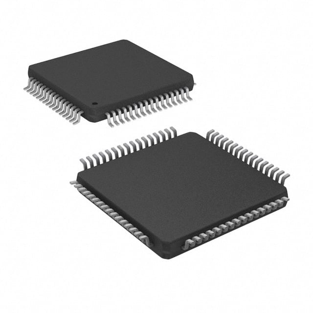
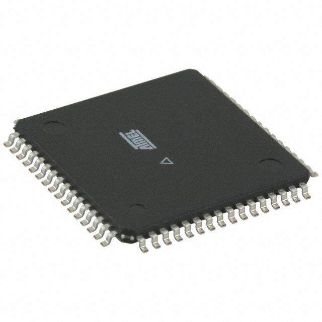
| 供应商器件封装 | 64-TQFP(14x14) |
| 其它名称 | ATMEGA128AAU |
| 包装 | 托盘 |
| 可用A/D通道 | 8 |
| 可编程输入/输出端数量 | 53 |
| 商标 | Atmel |
| 商标名 | ATMEGA |
| 处理器系列 | megaAVR |
| 外设 | 欠压检测/复位,POR,PWM,WDT |
| 安装风格 | SMD/SMT |
| 定时器数量 | 4 Timer |
| 封装/外壳 | 64-TQFP |
| 封装/箱体 | TQFP-64 |
| 工作温度 | -40°C ~ 85°C |
| 工作电源电压 | 2.7 V to 5.5 V |
| 工厂包装数量 | 90 |
| 振荡器类型 | 内部 |
| 接口类型 | JTAG |
| 数据RAM大小 | 4 kB |
| 数据Ram类型 | SRAM |
| 数据ROM大小 | 4 kB |
| 数据Rom类型 | EEPROM |
| 数据总线宽度 | 8 bit |
| 数据转换器 | A/D 8x10b |
| 最大工作温度 | + 85 C |
| 最大时钟频率 | 16 MHz |
| 最小工作温度 | - 40 C |
| 标准包装 | 90 |
| 核心 | AVR |
| 核心处理器 | AVR |
| 核心尺寸 | 8-位 |
| 片上ADC | Yes |
| 电压-电源(Vcc/Vdd) | 2.7 V ~ 5.5 V |
| 程序存储器大小 | 128 kB |
| 程序存储器类型 | Flash |
| 程序存储容量 | 128KB(64K x 16) |
| 系列 | ATMEGA 128A |
| 输入/输出端数量 | 53 I/O |
| 连接性 | EBI/EMI, I²C, SPI, UART/USART |
| 速度 | 16MHz |
| 配用 | /product-detail/zh/ATSTK600-RC09/ATSTK600-RC09-ND/2271089 |


- 商务部:美国ITC正式对集成电路等产品启动337调查
- 曝三星4nm工艺存在良率问题 高通将骁龙8 Gen1或转产台积电
- 太阳诱电将投资9.5亿元在常州建新厂生产MLCC 预计2023年完工
- 英特尔发布欧洲新工厂建设计划 深化IDM 2.0 战略
- 台积电先进制程称霸业界 有大客户加持明年业绩稳了
- 达到5530亿美元!SIA预计今年全球半导体销售额将创下新高
- 英特尔拟将自动驾驶子公司Mobileye上市 估值或超500亿美元
- 三星加码芯片和SET,合并消费电子和移动部门,撤换高东真等 CEO
- 三星电子宣布重大人事变动 还合并消费电子和移动部门
- 海关总署:前11个月进口集成电路产品价值2.52万亿元 增长14.8%


PDF Datasheet 数据手册内容提取
8-bit AVR Microcontroller ATmega128A DATASHEET COMPLETE Introduction The Atmel® ATmega128A is a low-power CMOS 8-bit microcontroller based on the AVR® enhanced RISC architecture. By executing powerful instructions in a single clock cycle, the ATmega128A achieves throughputs close to 1MIPS per MHz. This empowers system designer to optimize the device for power consumption versus processing speed. Features • High-performance, Low-power Atmel AVR 8-bit Microcontroller • Advanced RISC Architecture – 133 Powerful Instructions - Most Single-clock Cycle Execution – 32 × 8 General Purpose Working Registers + Peripheral Control Registers – Fully Static Operation – Up to 16MIPS Throughput at 16MHz – On-chip 2-cycle Multiplier • High Endurance Non-volatile Memory segments – 128Kbytes of In-System Self-programmable Flash program memory – 4Kbytes EEPROM – 4Kbytes Internal SRAM – Write/Erase cycles: 10,000 Flash/100,000 EEPROM – Data retention: 20 years at 85°C/100 years at 25°C(1) – Optional Boot Code Section with Independent Lock Bits • In-System Programming by On-chip Boot Program • True Read-While-Write Operation – Up to 64 Kbytes Optional External Memory Space – Programming Lock for Software Security – SPI Interface for In-System Programming • JTAG (IEEE std. 1149.1 Compliant) Interface – Boundary-scan Capabilities According to the JTAG Standard – Extensive On-chip Debug Support Atmel-8151J-8-bit AVR Microcontroller_Datasheet_Complete-09/2015
– Programming of Flash, EEPROM, Fuses and Lock Bits through the JTAG Interface • Atmel QTouch® library support – Capacitive touch buttons, sliders and wheels – Atmel QTouch and QMatrix acquisition – Up to 64 sense channels • Peripheral Features – Two 8-bit Timer/Counters with Separate Prescalers and Compare Modes – Two Expanded 16-bit Timer/Counters with Separate Prescaler, Compare Mode and Capture Mode – Real Time Counter with Separate Oscillator – Two 8-bit PWM Channels – 6 PWM Channels with Programmable Resolution from 2 to 16 Bits – Output Compare Modulator – 8-channel, 10-bit ADC • 8 Single-ended Channels • 7 Differential Channels • 2 Differential Channels with Programmable Gain at 1x, 10x, or 200x – Byte-oriented Two-wire Serial Interface – Dual Programmable Serial USARTs – Master/Slave SPI Serial Interface – Programmable Watchdog Timer with On-chip Oscillator – On-chip Analog Comparator • Special Microcontroller Features – Power-on Reset and Programmable Brown-out Detection – Internal Calibrated RC Oscillator – External and Internal Interrupt Sources – Six Sleep Modes: Idle, ADC Noise Reduction, Power-save, Power-down, Standby, and Extended Standby – Software Selectable Clock Frequency – ATmega103 Compatibility Mode Selected by a Fuse – Global Pull-up Disable • I/O and Packages – 53 Programmable I/O Lines – 64-lead TQFP and 64-pad QFN/MLF • Operating Voltages – 2.7 - 5.5V • Speed Grades – 0 - 16MHz Atmel ATmega128A [DATASHEET] 2 Atmel-8151J-8-bit AVR Microcontroller_Datasheet_Complete-09/2015
Table of Contents Introduction......................................................................................................................1 Features..........................................................................................................................1 1. Description.................................................................................................................9 2. Configuration Summary...........................................................................................10 3. Ordering Information................................................................................................11 4. Block Diagram.........................................................................................................12 5. ATmega103 and ATmega128A Compatibility..........................................................13 5.1. ATmega103 Compatibility Mode.................................................................................................13 6. Pin Configurations...................................................................................................14 6.1. Pin Descriptions..........................................................................................................................14 7. Resources................................................................................................................18 8. Data Retention.........................................................................................................19 9. About Code Examples.............................................................................................20 10.Capacitive Touch Sensing.......................................................................................21 11. AVR CPU Core........................................................................................................22 11.1. Overview.....................................................................................................................................22 11.2. ALU – Arithmetic Logic Unit........................................................................................................23 11.3. Status Register...........................................................................................................................23 11.4. General Purpose Register File...................................................................................................25 11.5. Stack Pointer..............................................................................................................................26 11.6. Instruction Execution Timing......................................................................................................28 11.7. Reset and Interrupt Handling.....................................................................................................29 12.AVR Memories.........................................................................................................32 12.1. Overview.....................................................................................................................................32 12.2. In-System Reprogrammable Flash Program Memory................................................................32 12.3. SRAM Data Memory...................................................................................................................33 12.4. EEPROM Data Memory.............................................................................................................35 12.5. I/O Memory.................................................................................................................................36 12.6. External Memory Interface.........................................................................................................36 12.7. Register Description...................................................................................................................43 13.System Clock and Clock Options............................................................................54 13.1. Clock Systems and their Distribution..........................................................................................54 13.2. Clock Sources............................................................................................................................55
13.3. Default Clock Source..................................................................................................................56 13.4. Crystal Oscillator........................................................................................................................56 13.5. Low-frequency Crystal Oscillator................................................................................................57 13.6. External RC Oscillator................................................................................................................58 13.7. Calibrated Internal RC Oscillator................................................................................................58 13.8. External Clock............................................................................................................................59 13.9. Timer/Counter Oscillator.............................................................................................................60 13.10.Register Description...................................................................................................................60 14.Power Management and Sleep Modes...................................................................63 14.1. Sleep Modes...............................................................................................................................63 14.2. Idle Mode....................................................................................................................................64 14.3. ADC Noise Reduction Mode.......................................................................................................64 14.4. Power-down Mode......................................................................................................................64 14.5. Power-save Mode.......................................................................................................................64 14.6. Standby Mode............................................................................................................................65 14.7. Extended Standby Mode............................................................................................................65 14.8. Minimizing Power Consumption.................................................................................................65 14.9. Register Description...................................................................................................................67 15.System Control and Reset.......................................................................................69 15.1. Resetting the AVR......................................................................................................................69 15.2. Reset Sources............................................................................................................................69 15.3. Internal Voltage Reference.........................................................................................................73 15.4. Watchdog Timer.........................................................................................................................73 15.5. Timed Sequences for Changing the Configuration of the Watchdog Timer...............................74 15.6. Register Description...................................................................................................................75 16.Interrupts.................................................................................................................79 16.1. Interrupt Vectors in ATmega128A...............................................................................................79 16.2. Register Description...................................................................................................................84 17.External Interrupts...................................................................................................87 17.1. Register Description...................................................................................................................87 18.I/O Ports..................................................................................................................94 18.1. Overview.....................................................................................................................................94 18.2. Ports as General Digital I/O........................................................................................................95 18.3. Alternate Port Functions.............................................................................................................99 18.4. Register Description.................................................................................................................113 19.Timer/Counter3, Timer/Counter2, and Timer/Counter1 Prescalers.......................136 19.1. Overview...................................................................................................................................136 19.2. Internal Clock Source...............................................................................................................136 19.3. Prescaler Reset........................................................................................................................136 19.4. External Clock Source..............................................................................................................136 19.5. Register Description.................................................................................................................137 20.16-bit Timer/Counter (Timer/Counter1 and Timer/Counter3).................................139 Atmel ATmega128A [DATASHEET] 4 Atmel-8151J-8-bit AVR Microcontroller_Datasheet_Complete-09/2015
20.1. Features...................................................................................................................................139 20.2. Overview...................................................................................................................................139 20.3. Accessing 16-bit Registers.......................................................................................................142 20.4. Timer/Counter Clock Sources..................................................................................................144 20.5. Counter Unit.............................................................................................................................144 20.6. Input Capture Unit....................................................................................................................145 20.7. Output Compare Units..............................................................................................................148 20.8. Compare Match Output Unit.....................................................................................................149 20.9. Modes of Operation..................................................................................................................150 20.10.Timer/Counter Timing Diagrams..............................................................................................158 20.11.Register Description.................................................................................................................159 21.8-bit Timer/Counter0 with PWM and Asynchronous Operation.............................194 21.1. Features...................................................................................................................................194 21.2. Overview...................................................................................................................................194 21.3. Timer/Counter Clock Sources..................................................................................................195 21.4. Counter Unit.............................................................................................................................195 21.5. Output Compare Unit................................................................................................................196 21.6. Compare Match Output Unit.....................................................................................................198 21.7. Modes of Operation..................................................................................................................199 21.8. Timer/Counter Timing Diagrams...............................................................................................203 21.9. Asynchronous Operation of the Timer/Counter........................................................................205 21.10.Timer/Counter Prescaler..........................................................................................................206 21.11.Register Description.................................................................................................................207 22.8-bit Timer/Counter2 with PWM.............................................................................217 22.1. Features...................................................................................................................................217 22.2. Overview...................................................................................................................................217 22.3. Timer/Counter Clock Sources..................................................................................................218 22.4. Counter Unit.............................................................................................................................218 22.5. Output Compare Unit................................................................................................................219 22.6. Compare Match Output Unit.....................................................................................................221 22.7. Modes of Operation..................................................................................................................222 22.8. Timer/Counter Timing Diagrams...............................................................................................226 22.9. Register Description.................................................................................................................227 23.Output Compare Modulator (OCM1C2).................................................................235 23.1. Overview...................................................................................................................................235 23.2. Description................................................................................................................................235 24.SPI – Serial Peripheral Interface...........................................................................237 24.1. Features...................................................................................................................................237 24.2. Overview...................................................................................................................................237 24.3. SS Pin Functionality.................................................................................................................240 24.4. Data Modes..............................................................................................................................241 24.5. Register Description.................................................................................................................242 25.USART...................................................................................................................247 25.1. Features...................................................................................................................................247 Atmel ATmega128A [DATASHEET] 5 Atmel-8151J-8-bit AVR Microcontroller_Datasheet_Complete-09/2015
25.2. Overview...................................................................................................................................247 25.3. Clock Generation......................................................................................................................249 25.4. Frame Formats.........................................................................................................................252 25.5. USART Initialization..................................................................................................................253 25.6. Data Transmission – The USART Transmitter.........................................................................254 25.7. Data Reception – The USART Receiver..................................................................................257 25.8. Asynchronous Data Reception.................................................................................................260 25.9. Multi-Processor Communication Mode.....................................................................................263 25.10.Examples of Baud Rate Setting...............................................................................................264 25.11.Register Description.................................................................................................................267 26.TWI - Two-wire Serial Interface.............................................................................276 26.1. Features...................................................................................................................................276 26.2. Overview...................................................................................................................................276 26.3. Two-Wire Serial Interface Bus Definition..................................................................................278 26.4. Data Transfer and Frame Format.............................................................................................279 26.5. Multi-master Bus Systems, Arbitration and Synchronization....................................................282 26.6. Using the TWI...........................................................................................................................283 26.7. Multi-master Systems and Arbitration.......................................................................................300 26.8. Register Description.................................................................................................................301 27.Analog Comparator...............................................................................................308 27.1. Overview...................................................................................................................................308 27.2. Analog Comparator Multiplexed Input......................................................................................308 27.3. Register Description.................................................................................................................309 28.ADC - Analog to Digital Converter.........................................................................313 28.1. Features...................................................................................................................................313 28.2. Overview...................................................................................................................................313 28.3. Starting a Conversion...............................................................................................................315 28.4. Prescaling and Conversion Timing...........................................................................................315 28.5. Changing Channel or Reference Selection..............................................................................317 28.6. ADC Noise Canceler................................................................................................................319 28.7. ADC Conversion Result............................................................................................................322 28.8. Register Description.................................................................................................................324 29.JTAG Interface and On-chip Debug System..........................................................334 29.1. Features...................................................................................................................................334 29.2. Overview...................................................................................................................................334 29.3. TAP – Test Access Port............................................................................................................335 29.4. TAP Controller..........................................................................................................................336 29.5. Using the Boundary-scan Chain...............................................................................................337 29.6. Using the On-chip Debug System............................................................................................337 29.7. On-chip Debug Specific JTAG Instructions..............................................................................338 29.8. Using the JTAG Programming Capabilities..............................................................................339 29.9. Bibliography..............................................................................................................................339 29.10.IEEE 1149.1 (JTAG) Boundary-scan........................................................................................339 29.11.Data Registers..........................................................................................................................340 29.12.Boundry-scan Specific JTAG Instructions................................................................................342 Atmel ATmega128A [DATASHEET] 6 Atmel-8151J-8-bit AVR Microcontroller_Datasheet_Complete-09/2015
29.13.Boundary-scan Chain...............................................................................................................343 29.14.ATmega128A Boundary-scan Order........................................................................................353 29.15.Boundary-scan Description Language Files............................................................................362 29.16.Register Description.................................................................................................................362 30.Boot Loader Support – Read-While-Write Self-Programming...............................365 30.1. Features...................................................................................................................................365 30.2. Overview...................................................................................................................................365 30.3. Application and Boot Loader Flash Sections............................................................................365 30.4. Read-While-Write and No Read-While-Write Flash Sections...................................................366 30.5. Boot Loader Lock Bits..............................................................................................................368 30.6. Entering the Boot Loader Program...........................................................................................369 30.7. Addressing the Flash During Self-Programming......................................................................370 30.8. Self-Programming the Flash.....................................................................................................371 30.9. Register Description.................................................................................................................379 31.Memory Programming...........................................................................................382 31.1. Program and Data Memory Lock Bits.......................................................................................382 31.2. Fuse Bits...................................................................................................................................383 31.3. Signature Bytes........................................................................................................................385 31.4. Calibration Byte........................................................................................................................385 31.5. Page Size.................................................................................................................................386 31.6. Parallel Programming Parameters, Pin Mapping, and Commands..........................................386 31.7. Parallel Programming...............................................................................................................388 31.8. Serial Downloading...................................................................................................................395 31.9. Serial Programming Pin Mapping.............................................................................................396 31.10.Programming Via the JTAG Interface.......................................................................................400 32.Electrical Characteristics.......................................................................................414 32.1. DC Characteristics....................................................................................................................414 32.2. Speed Grades..........................................................................................................................416 32.3. Clock Characteristics................................................................................................................416 32.4. System and Reset Characteristics...........................................................................................417 32.5. Two-wire Serial Interface Characteristics.................................................................................418 32.6. Parallel Programming Characteristics......................................................................................419 32.7. SPI Timing Characteristics.......................................................................................................421 32.8. ADC Characteristics.................................................................................................................423 32.9. External Data Memory Timing..................................................................................................426 33.Typical Characteristics...........................................................................................432 33.1. Active Supply Current...............................................................................................................432 33.2. Idle Supply Current...................................................................................................................436 33.3. Power-down Supply Current.....................................................................................................439 33.4. Power-save Supply Current......................................................................................................440 33.5. Standby Supply Current...........................................................................................................441 33.6. Pin Pull-up................................................................................................................................442 33.7. Pin Driver Strength...................................................................................................................443 33.8. Pin Thresholds and Hysteresis.................................................................................................445 33.9. BOD Thresholds and Analog Comparator Offset.....................................................................446 Atmel ATmega128A [DATASHEET] 7 Atmel-8151J-8-bit AVR Microcontroller_Datasheet_Complete-09/2015
33.10.Internal Oscillator Speed..........................................................................................................448 33.11.Current Consumption of Peripheral Units.................................................................................454 33.12.Current Consumption in Reset and Reset Pulse width............................................................457 34.Register Summary.................................................................................................461 35.Instruction Set Summary.......................................................................................464 36.Packaging Information...........................................................................................469 36.1. 64A...........................................................................................................................................469 36.2. 64M1.........................................................................................................................................470 37.Errata.....................................................................................................................471 37.1. ATmega128A Rev. U................................................................................................................471 38.Datasheet Revision History...................................................................................473 38.1. Rev. 8151J – 07/2015...............................................................................................................473 38.2. Rev. 8151I – 08/2014...............................................................................................................473 38.3. Rev. 8151H – 02/11..................................................................................................................473 38.4. Rev. 8151G – 07/10..................................................................................................................473 38.5. Rev. 8151F – 06/10..................................................................................................................473 38.6. Rev. 8151E – 02/10..................................................................................................................473 38.7. Rev. 8151D – 07/09..................................................................................................................473 38.8. Rev. 8151C – 05/09..................................................................................................................474 38.9. Rev. 8151B – 03/09..................................................................................................................474 38.10.Rev. 8151A – 08/08..................................................................................................................474 Atmel ATmega128A [DATASHEET] 8 Atmel-8151J-8-bit AVR Microcontroller_Datasheet_Complete-09/2015
1. Description The Atmel AVR core combines a rich instruction set with 32 general purpose working registers. All the 32 registers are directly connected to the Arithmetic Logic Unit (ALU), allowing two independent registers to be accessed in one single instruction executed in one clock cycle. The resulting architecture is more code efficient while achieving throughputs up to ten times faster than conventional CISC microcontrollers. The ATmega128A provides the following features: 128Kbytes of In-System Programmable Flash with Read- While-Write capabilities, 4Kbytes EEPROM, 4Kbytes SRAM, 53 general purpose I/O lines, 32 general purpose working registers, Real Time Counter (RTC), four flexible Timer/Counters with compare modes and PWM, 2 USARTs, one byte oriented Two-wire Serial Interface, an 8-channel, 10-bit ADC with optional differential input stage with programmable gain, programmable Watchdog Timer with Internal Oscillator, one SPI serial port, IEEE std. 1149.1 compliant JTAG test interface, also used for accessing the On-chip Debug system and programming and six software selectable power saving modes. The Idle mode stops the CPU while allowing the SRAM, Timer/Counters, SPI port, and interrupt system to continue functioning. The Power-down mode saves the register contents but freezes the Oscillator, disabling all other chip functions until the next interrupt or Hardware Reset. In Power-save mode, the asynchronous timer continues to run, allowing the user to maintain a timer base while the rest of the device is sleeping. The ADC Noise Reduction mode stops the CPU and all I/O modules except Asynchronous Timer and ADC, to minimize switching noise during ADC conversions. In Standby mode, the Crystal/Resonator Oscillator is running while the rest of the device is sleeping. This allows very fast start-up combined with low power consumption. In Extended Standby mode, both the main Oscillator and the Asynchronous Timer continue to run. The device is manufactured using Atmel’s high-density nonvolatile memory technology. The On-chip ISP Flash allows the program memory to be reprogrammed in-system through an SPI serial interface, by a conventional nonvolatile memory programmer, or by an On-chip Boot program running on the AVR core. The boot program can use any interface to download the application program in the application Flash memory. Software in the Boot Flash section will continue to run while the Application Flash section is updated, providing true Read- While-Write operation. By combining an 8-bit RISC CPU with In-System Self-Programmable Flash on a monolithic chip, the Atmel ATmega128A is a powerful microcontroller that provides a highly flexible and cost effective solution to many embedded control application The ATmega128A AVR is supported with a full suite of program and system development tools including: C compilers, macro assemblers, program debugger/simulators, in-circuit emulators, and evaluation kits. Atmel ATmega128A [DATASHEET] 9 Atmel-8151J-8-bit AVR Microcontroller_Datasheet_Complete-09/2015
2. Configuration Summary Features ATmega128A Pin count 64 Flash (KB) 128 SRAM (KB) 4 EEPROM (KB) 4 External Memory (KB) 64 General Purpose I/O pins 53 SPI 1 TWI (I2C) 1 USART 2 ADC 10-bit, up to 76.9ksps (15ksps at max resolution) ADC channels 6 (8 in TQFP and QFN/MLF packages) AC propagation delay Typ 400ns 8-bit Timer/Counters 2 16-bit Timer/Counters 2 PWM channels 6 RC Oscillator +/-3% VREF Bandgap Operating voltage 2.7 - 5.5V Max operating frequency 16MHz Temperature range -55°C to +125°C JTAG Yes Atmel ATmega128A [DATASHEET] 10 Atmel-8151J-8-bit AVR Microcontroller_Datasheet_Complete-09/2015
3. Ordering Information Speed (MHz) Power Supply Ordering Code(2) Package(1) Operational Range ATmega128A-AU 64A ATmega128A-AUR(3) 64A 16 2.7 - 5.5V Industrial (-40oC to 85oC) ATmega128A-MU 64M1 ATmega128A-MUR(3) 64M1 Note: 1. This device can also be supplied in wafer form. Please contact your local Atmel sales office for detailed ordering information and minimum quantities. 2. Pb-free packaging, complies to the European Directive for Restriction of Hazardous Substances (RoHS directive). Also Halide free and fully Green. 3. Tape and Reel Package Type 64A 64-lead, 14 × 14 × 1.0 mm, Thin Profile Plastic Quad Flat Package (TQFP) 64M1 64-pad, 9 × 9 × 1.0 mm, Quad Flat No-Lead/Micro Lead Frame Package (QFN/MLF) Atmel ATmega128A [DATASHEET] 11 Atmel-8151J-8-bit AVR Microcontroller_Datasheet_Complete-09/2015
4. Block Diagram Figure 4-1 Block Diagram SRAM TCK CPU TTMDSI JTAG OCD FLASH TDO PARPROG NVM PEN programming EEPROM PDI EEPROMIF SERPROG PDO SCK AD[7:0] ExtMem A[15:8] Clock generation RD/WR/ALE XTAL1 8MHz 8MHz Power D A Crystal Osc Calib RC management T PA[7:0] PB[7:0] XTAL2 ER1xC2tMe OrHnszacl Exctloercnkal ancdo nctlrooclk AB POI/ROTS PPCD[[77::00]] TOSC1 U PE[7:0] 32.768kHz 1MHz int S PF[7:0] XOSC osc PG[4:0] TOSC2 ExtInt INT[7:0] VCC Power Watchdog Supervision Timer RESET ADC ADC[7:0] POR/BOD & AREF RESET GND Internal AIN0 Reference AC AIN1 ACO ADCMUX MISO MOSI SPI TC 0 SCK (8-bit async) OC0 SS SSDCAL TWI (1T6C-bi t)1 OT1C1A/B/C ICP1 RTxxDD00 USART 0 TC 2 T2 (8-bit) OC2 XCK0 RxD1 TC 3 OC3A/B TxD1 USART 1 (16-bit) T3 XCK1 ICP3 Atmel ATmega128A [DATASHEET] 12 Atmel-8151J-8-bit AVR Microcontroller_Datasheet_Complete-09/2015
5. ATmega103 and ATmega128A Compatibility The ATmega128A is a highly complex microcontroller where the number of I/O locations supersedes the 64 I/O locations reserved in the AVR instruction set. To ensure backward compatibility with the ATmega103, all I/O locations present in ATmega103 have the same location in ATmega128A. Most additional I/O locations are added in an Extended I/O space starting from 0x60 to 0xFF, (that is, in the ATmega103 internal RAM space). These locations can be reached by using LD/LDS/LDD and ST/STS/STD instructions only, not by using IN and OUT instructions. The relocation of the internal RAM space may still be a problem for ATmega103 users. Also, the increased number of interrupt vectors might be a problem if the code uses absolute addresses. To solve these problems, an ATmega103 compatibility mode can be selected by programming the fuse M103C. In this mode, none of the functions in the Extended I/O space are in use, so the internal RAM is located as in ATmega103. Also, the Extended Interrupt vectors are removed. The Atmel AVR ATmega128A is 100% pin compatible with ATmega103, and can replace the ATmega103 on current Printed Circuit Boards. The application note “Replacing ATmega103 by ATmega128A” describes what the user should be aware of replacing the ATmega103 by an ATmega128A. 5.1. ATmega103 Compatibility Mode By programming the M103C fuse, the ATmega128A will be compatible with the ATmega103 regards to RAM, I/O pins and interrupt vectors as described above. However, some new features in ATmega128A are not available in this compatibility mode, these features are listed below: • One USART instead of two, Asynchronous mode only. Only the eight least significant bits of the Baud Rate Register is available. • One 16 bits Timer/Counter with two compare registers instead of two 16-bit Timer/Counters with three compare registers. • Two-wire serial interface is not supported. • Port C is output only. • Port G serves alternate functions only (not a general I/O port). • Port F serves as digital input only in addition to analog input to the ADC. • Boot Loader capabilities is not supported. • It is not possible to adjust the frequency of the internal calibrated RC Oscillator. • The External Memory Interface can not release any Address pins for general I/O, neither configure different wait-states to different External Memory Address sections. • In addition, there are some other minor differences to make it more compatible to ATmega103: • Only EXTRF and PORF exists in MCUCSR. • Timed sequence not required for Watchdog Time-out change. • External Interrupt pins 3 - 0 serve as level interrupt only. • USART has no FIFO buffer, so data overrun comes earlier. Unused I/O bits in ATmega103 should be written to 0 to ensure same operation in ATmega128A. Atmel ATmega128A [DATASHEET] 13 Atmel-8151J-8-bit AVR Microcontroller_Datasheet_Complete-09/2015
6. Pin Configurations Figure 6-1 Pinout ATmega128A Power Ground Programming/debug Digital Analog CK) MS) DO) DI) T T T T Crystal/Osc C0) C1) C2) C3) C4/ C5/ C6/ C7/ 0) 1) 2) D D D D D D D D D D D External Memory VCC ND REF F0 (A F1 (A F2 (A F3 (A F4 (A F5 (A F6 (A F7 (A ND CC A0 (A A1 (A A2 (A A G A P P P P P P P P G V P P P 4 3 2 1 0 9 8 7 6 5 4 3 2 1 0 9 6 6 6 6 6 5 5 5 5 5 5 5 5 5 5 4 PEN 1 48 PA3 (AD3) (RXD0/PDI) PE0 2 47 PA4 (AD4) (TXD0/PDO) PE1 3 46 PA5 (AD5) (XCK0/AIN0) PE2 4 45 PA6 (AD6) (OC3A/AIN1) PE3 5 44 PA7 (AD7) (OC3B/INT4) PE4 6 43 PG2 (ALE) (OC3C/INT5) PE5 7 42 PC7 (A15) (T3/INT6) PE6 8 41 PC6 (A14) (ICP3/INT7) PE7 9 40 PC5 (A13) (SS) PB0 10 39 PC4 (A12) (SCK) PB1 11 38 PC3 (A11) (MOSI) PB2 12 37 PC2 (A10) (MISO) PB3 13 36 PC1 (A9) (OC0) PB4 14 35 PC0 (A8) (OC1A) PB5 15 34 PG1 (RD) (OC1B) PB6 16 33 PG0 (WR) 7 8 9 0 1 2 3 4 5 6 7 8 9 0 1 2 1 1 1 2 2 2 2 2 2 2 2 2 2 3 3 3 7 3 4 T C D 2 1 0 1 2 3 4 5 6 7 B G G E C N L L D D D D D D D D C) P 2) P 1) P RES V G XTA XTA 0) P 1) P 2) P 3) P 1) P 1) P 1) P 2) P 1 C C T T T T P K T T C S S N N N N C C ( ( C2/O (TO (TO CL/I DA/I D1/I D1/I (I (X (O (S (S (RX (TX Note: The Pinout figure applies to both TQFP and MLF packages. The bottom pad under the QFN/MLF package should be soldered to ground. 6.1. Pin Descriptions 6.1.1. V CC Digital supply voltage. Atmel ATmega128A [DATASHEET] 14 Atmel-8151J-8-bit AVR Microcontroller_Datasheet_Complete-09/2015
6.1.2. GND Ground. 6.1.3. Port A (PA7:PA0) Port A is an 8-bit bi-directional I/O port with internal pull-up resistors (selected for each bit). The Port A output buffers have symmetrical drive characteristics with both high sink and source capability. As inputs, Port A pins that are externally pulled low will source current if the pull-up resistors are activated. The Port A pins are tristated when a reset condition becomes active, even if the clock is not running. Port A also serves the functions of various special features of the ATmega128A as listed in Alternate Functions of Port A. Related Links Alternate Functions of Port A on page 100 6.1.4. Port B (PB7:PB0) Port B is an 8-bit bi-directional I/O port with internal pull-up resistors (selected for each bit). The Port B output buffers have symmetrical drive characteristics with both high sink and source capability. As inputs, Port B pins that are externally pulled low will source current if the pull-up resistors are activated. The Port B pins are tristated when a reset condition becomes active, even if the clock is not running. Port B also serves the functions of various special features of the ATmega128A as listed in Alternate Functions of Port B. Related Links Alternate Functions of Port B on page 102 6.1.5. Port C (PC7:PC0) Port C is an 8-bit bi-directional I/O port with internal pull-up resistors (selected for each bit). The Port C output buffers have symmetrical drive characteristics with both high sink and source capability. As inputs, Port C pins that are externally pulled low will source current if the pull-up resistors are activated. The Port C pins are tristated when a reset condition becomes active, even if the clock is not running. Port C also serves the functions of special features of the ATmega128A as listed in Alternate Functions of Port C. In ATmega103 compatibility mode, Port C is output only, and the port C pins are not tri-stated when a reset condition becomes active. Note: The Atmel AVR ATmega128A is by default shipped in ATmega103 compatibility mode. Thus, if the parts are not programmed before they are put on the PCB, PORTC will be output during first power up, and until the ATmega103 compatibility mode is disabled. Related Links Alternate Functions of Port C on page 104 6.1.6. Port D (PD7:PD0) Port D is an 8-bit bi-directional I/O port with internal pull-up resistors (selected for each bit). The Port D output buffers have symmetrical drive characteristics with both high sink and source capability. As inputs, Port D pins that are externally pulled low will source current if the pull-up resistors are activated. The Port D pins are tristated when a reset condition becomes active, even if the clock is not running. Port D also serves the functions of various special features of the ATmega128A as listed in Alternate Functions of Port D. Related Links Alternate Functions of Port D on page 106 Atmel ATmega128A [DATASHEET] 15 Atmel-8151J-8-bit AVR Microcontroller_Datasheet_Complete-09/2015
6.1.7. Port E (PE7:PE0) Port E is an 8-bit bi-directional I/O port with internal pull-up resistors (selected for each bit). The Port E output buffers have symmetrical drive characteristics with both high sink and source capability. As inputs, Port E pins that are externally pulled low will source current if the pull-up resistors are activated. The Port E pins are tristated when a reset condition becomes active, even if the clock is not running. Port E also serves the functions of various special features of the ATmega128A as listed in Alternate Functions of Port E. Related Links Alternate Functions of Port E on page 108 6.1.8. Port F (PF7:PF0) Port F serves as the analog inputs to the A/D Converter. Port F also serves as an 8-bit bi-directional I/O port, if the A/D Converter is not used. Port pins can provide internal pull-up resistors (selected for each bit). The Port F output buffers have symmetrical drive characteristics with both high sink and source capability. As inputs, Port F pins that are externally pulled low will source current if the pull-up resistors are activated. The Port F pins are tri-stated when a reset condition becomes active, even if the clock is not running. If the JTAG interface is enabled, the pull-up resistors on pins PF7(TDI), PF5(TMS), and PF4(TCK) will be activated even if a Reset occurs. The TDO pin is tri-stated unless TAP states that shift out data are entered. Port F also serves the functions of the JTAG interface. In ATmega103 compatibility mode, Port F is an input Port only. 6.1.9. Port G (PG4:PG0) Port G is a 5-bit bi-directional I/O port with internal pull-up resistors (selected for each bit). The Port G output buffers have symmetrical drive characteristics with both high sink and source capability. As inputs, Port G pins that are externally pulled low will source current if the pull-up resistors are activated. The Port G pins are tristated when a reset condition becomes active, even if the clock is not running. Port G also serves the functions of various special features. The port G pins are tri-stated when a reset condition becomes active, even if the clock is not running. In Atmel AVR ATmega103 compatibility mode, these pins only serves as strobes signals to the external memory as well as input to the 32kHz Oscillator, and the pins are initialized to PG0 = 1, PG1 = 1, and PG2 = 0 asynchronously when a reset condition becomes active, even if the clock is not running. PG3 and PG4 are oscillator pins. 6.1.10. RESET Reset input. A low level on this pin for longer than the minimum pulse length will generate a reset, even if the clock is not running. The minimum pulse length is given in System and Reset Characteristics. Shorter pulses are not guaranteed to generate a reset. Related Links System and Reset Characteristics on page 417 6.1.11. XTAL1 Input to the inverting Oscillator amplifier and input to the internal clock operating circuit. 6.1.12. XTAL2 Output from the inverting Oscillator amplifier. Atmel ATmega128A [DATASHEET] 16 Atmel-8151J-8-bit AVR Microcontroller_Datasheet_Complete-09/2015
6.1.13. AV CC AV is the supply voltage pin for Port F and the A/D Converter. It should be externally connected to V , CC CC even if the ADC is not used. If the ADC is used, it should be connected to V through a low-pass filter. CC 6.1.14. AREF AREF is the analog reference pin for the A/D Converter. 6.1.15. PEN PEN is a programming enable pin for the SPI Serial Programming mode, and is internally pulled high. By holding this pin low during a Power-on Reset, the device will enter the SPI Serial Programming mode. PEN has no function during normal operation. Atmel ATmega128A [DATASHEET] 17 Atmel-8151J-8-bit AVR Microcontroller_Datasheet_Complete-09/2015
7. Resources A comprehensive set of development tools, application notes and datasheets are available for download on http://www.atmel.com/avr. Atmel ATmega128A [DATASHEET] 18 Atmel-8151J-8-bit AVR Microcontroller_Datasheet_Complete-09/2015
8. Data Retention Reliability Qualification results show that the projected data retention failure rate is much less than 1 PPM over 20 years at 85°C or 100 years at 25°C. Atmel ATmega128A [DATASHEET] 19 Atmel-8151J-8-bit AVR Microcontroller_Datasheet_Complete-09/2015
9. About Code Examples This datasheet contains simple code examples that briefly show how to use various parts of the device. These code examples assume that the part specific header file is included before compilation. Be aware that not all C compiler vendors include bit definitions in the header files and interrupt handling in C is compiler dependent. Please confirm with the C compiler documentation for more details. For I/O registers located in extended I/O map, “IN”, “OUT”, “SBIS”, “SBIC”, “CBI”, and “SBI” instructions must be replaced with instructions that allow access to extended I/O. Typically “LDS” and “STS” combined with “SBRS”, “SBRC”, “SBR”, and “CBR”. Atmel ATmega128A [DATASHEET] 20 Atmel-8151J-8-bit AVR Microcontroller_Datasheet_Complete-09/2015
10. Capacitive Touch Sensing The Atmel QTouch Library provides a simple to use solution to realize touch sensitive interfaces on most Atmel AVR microcontrollers. The QTouch Library includes support for the QTouch and QMatrix® acquisition methods. Touch sensing can be added to any application by linking the appropriate Atmel QTouch Library for the AVR Microcontroller. This is done by using a simple set of APIs to define the touch channels and sensors, and then calling the touch sensing API’s to retrieve the channel information and determine the touch sensor states. The QTouch Library is FREE and downloadable from the Atmel website at the following location: www.atmel.com/qtouchlibrary. For implementation details and other information, refer to the Atmel QTouch Library User Guide - also available for download from the Atmel website. Atmel ATmega128A [DATASHEET] 21 Atmel-8151J-8-bit AVR Microcontroller_Datasheet_Complete-09/2015
11. AVR CPU Core 11.1. Overview This section discusses the Atmel AVR core architecture in general. The main function of the CPU core is to ensure correct program execution. The CPU must therefore be able to access memories, perform calculations, control peripherals, and handle interrupts. Figure 11-1 Block Diagram of the AVR MCU Architecture Data Bus 8-bit Program Status Flash Counter and Control Program Memory Interrupt 32 x 8 Unit Instruction General Register Purpose SPI Registrers Unit Instruction Watchdog Decoder Timer g Control Lines Direct Addressing Indirect Addressin ALU Ci/OoAm Mnpaoaldoruaglteo1r Data i/O Module 2 SRAM i/O Module n EEPROM I/O Lines In order to maximize performance and parallelism, the AVR uses a Harvard architecture – with separate memories and buses for program and data. Instructions in the Program memory are executed with a single level pipelining. While one instruction is being executed, the next instruction is pre-fetched from the Program memory. This concept enables instructions to be executed in every clock cycle. The Program memory is In-System Reprogrammable Flash memory. The fast-access Register File contains 32 x 8-bit general purpose working registers with a single clock cycle access time. This allows single-cycle Arithmetic Logic Unit (ALU) operation. In a typical ALU operation, two operands are output from the Register File, the operation is executed, and the result is stored back in the Register File – in one clock cycle. Six of the 32 registers can be used as three 16-bit indirect address register pointers for Data Space addressing – enabling efficient address calculations. One of the these address pointers can also be used as an address pointer for look up tables in Flash Program memory. These added function registers are the 16-bit X-, Y-, and Z-register, described later in this section. The ALU supports arithmetic and logic operations between registers or between a constant and a register. Single register operations can also be executed in the ALU. After an arithmetic operation, the Status Register is updated to reflect information about the result of the operation. Atmel ATmega128A [DATASHEET] 22 Atmel-8151J-8-bit AVR Microcontroller_Datasheet_Complete-09/2015
The Program flow is provided by conditional and unconditional jump and call instructions, able to directly address the whole address space. Most AVR instructions have a single 16-bit word format. Every Program memory address contains a 16- or 32-bit instruction. Program Flash memory space is divided in two sections, the Boot program section and the Application program section. Both sections have dedicated Lock Bits for write and read/write protection. The SPM instruction that writes into the Application Flash memory section must reside in the Boot program section. During interrupts and subroutine calls, the return address Program Counter (PC) is stored on the Stack. The Stack is effectively allocated in the general data SRAM, and consequently the Stack size is only limited by the total SRAM size and the usage of the SRAM. All user programs must initialize the SP in the reset routine (before subroutines or interrupts are executed). The Stack Pointer SP is read/write accessible in the I/O space. The data SRAM can easily be accessed through the five different addressing modes supported in the AVR architecture. The memory spaces in the AVR architecture are all linear and regular memory maps. A flexible interrupt module has its control registers in the I/O space with an additional global interrupt enable bit in the Status Register. All interrupts have a separate Interrupt Vector in the Interrupt Vector table. The interrupts have priority in accordance with their Interrupt Vector position. The lower the Interrupt Vector address, the higher the priority. The I/O memory space contains 64 addresses for CPU peripheral functions as Control Registers, SPI, and other I/O functions. The I/O Memory can be accessed directly, or as the Data Space locations following those of the Register File, 0x20 - 0x5F. In addition, the ATmega128A has Extended I/O space from $60 in SRAM where only the ST/STS/STD and LD/LDS/LDD instructions can be used. 11.2. ALU – Arithmetic Logic Unit The high-performance Atmel AVR ALU operates in direct connection with all the 32 general purpose working registers. Within a single clock cycle, arithmetic operations between general purpose registers or between a register and an immediate are executed. The ALU operations are divided into three main categories – arithmetic, logical, and bit-functions. Some implementations of the architecture also provide a powerful multiplier supporting both signed/unsigned multiplication and fractional format. See the “Instruction Set” section for a detailed description. 11.3. Status Register The Status Register contains information about the result of the most recently executed arithmetic instruction. This information can be used for altering program flow in order to perform conditional operations. Note that the Status Register is updated after all ALU operations, as specified in the Instruction Set Reference. This will in many cases remove the need for using the dedicated compare instructions, resulting in faster and more compact code. The Status Register is not automatically stored when entering an interrupt routine and restored when returning from an interrupt. This must be handled by software. Atmel ATmega128A [DATASHEET] 23 Atmel-8151J-8-bit AVR Microcontroller_Datasheet_Complete-09/2015
11.3.1. SREG – The AVR Status Register When using the I/O specific commands IN and OUT, the I/O addresses 0x00 - 0x3F must be used. When addressing I/O Registers as data space using LD and ST instructions, 0x20 must be added to these offset addresses. The device is a complex microcontroller with more peripheral units than can be supported within the 64 location reserved in Opcode for the IN and OUT instructions. For the Extended I/O space from 0x60 in SRAM, only the ST/STS/STD and LD/LDS/LDD instructions can be used. Name: SREG Offset: 0x3F Reset: 0x00 Property:When addressing I/O Registers as data space the offset address is 0x5F Bit 7 6 5 4 3 2 1 0 I T H S V N Z C Access R/W R/W R/W R/W R/W R/W R/W R/W Reset 0 0 0 0 0 0 0 0 Bit 7 – I: Global Interrupt Enable The Global Interrupt Enable bit must be set for the interrupts to be enabled. The individual interrupt enable control is then performed in separate control registers. If the Global Interrupt Enable Register is cleared, none of the interrupts are enabled independent of the individual interrupt enable settings. The I- bit is cleared by hardware after an interrupt has occurred, and is set by the RETI instruction to enable subsequent interrupts. The I-bit can also be set and cleared by the application with the SEI and CLI instructions, as described in the Instruction Set Reference. Bit 6 – T: Bit Copy Storage The Bit Copy instructions BLD (Bit LoaD) and BST (Bit STore) use the T-bit as source or destination for the operated bit. A bit from a register in the Register File can be copied into T by the BST instruction, and a bit in T can be copied into a bit in a register in the Register File by the BLD instruction. Bit 5 – H: Half Carry Flag The Half Carry Flag H indicates a Half Carry in some arithmetic operations. Half Carry is useful in BCD arithmetic. See the “Instruction Set Description” for detailed information. Bit 4 – S: Sign Bit, S = N ⊕ V The S-bit is always an exclusive or between the Negative Flag N and the Two’s Complement Overflow Flag V. See the “Instruction Set Description” for detailed information. Bit 3 – V: Two’s Complement Overflow Flag The Two’s Complement Overflow Flag V supports two’s complement arithmetics. See the “Instruction Set Description” for detailed information. Bit 2 – N: Negative Flag The Negative Flag N indicates a negative result in an arithmetic or logic operation. See the “Instruction Set Description” for detailed information. Bit 1 – Z: Zero Flag The Zero Flag Z indicates a zero result in an arithmetic or logic operation. See the “Instruction Set Description” for detailed information. Atmel ATmega128A [DATASHEET] 24 Atmel-8151J-8-bit AVR Microcontroller_Datasheet_Complete-09/2015
Bit 0 – C: Carry Flag The Carry Flag C indicates a Carry in an arithmetic or logic operation. See the “Instruction Set Description” for detailed information. 11.4. General Purpose Register File The Register File is optimized for the Atmel AVR Enhanced RISC instruction set. In order to achieve the required performance and flexibility, the following input/output schemes are supported by the Register File: • One 8-bit output operand and one 8-bit result input. • Two 8-bit output operands and one 8-bit result input. • Two 8-bit output operands and one 16-bit result input. • One 16-bit output operand and one 16-bit result input. The following figure shows the structure of the 32 general purpose working registers in the CPU. Figure 11-2 AVR CPU General Purpose Working Registers 7 0 Addr. R0 0x00 R1 0x01 R2 0x02 … R13 0x0D General R14 0x0E Purpose R15 0x0F Working R16 0x10 Registers R17 0x11 … R26 0x1A X-register Low Byte R27 0x1B X-register High Byte R28 0x1C Y-register Low Byte R29 0x1D Y-register High Byte R30 0x1E Z-register Low Byte R31 0x1F Z-register High Byte Most of the instructions operating on the Register File have direct access to all registers, and most of them are single cycle instructions. As shown in the figure above, each register is also assigned a Data memory address, mapping them directly into the first 32 locations of the user Data Space. Although not being physically implemented as SRAM locations, this memory organization provides great flexibility in access of the registers, as the X-, Y-, and Z-pointer Registers can be set to index any register in the file. 11.4.1. The X-register, Y-register and Z-register The registers R26:R31 have some added functions to their general purpose usage. These registers are 16-bit address pointers for indirect addressing of the Data Space. The three indirect address registers X, Y and Z are defined as described in the following figure. Atmel ATmega128A [DATASHEET] 25 Atmel-8151J-8-bit AVR Microcontroller_Datasheet_Complete-09/2015
Figure 11-3 The X-, Y- and Z-Registers 15 XH XL 0 X-register 7 0 7 0 R27 (0x1B) R26 (0x1A) 15 YH YL 0 Y-register 7 0 7 0 R29 (0x1D) R28 (0x1C) 15 ZH ZL 0 Z-register 7 0 7 0 R31 (0x1F) R30 (0x1E) In the different addressing modes these address registers have functions as fixed displacement, automatic increment, and automatic decrement (see the Instruction Set Reference for details). 11.5. Stack Pointer The Stack is mainly used for storing temporary data, for storing local variables and for storing return addresses after interrupts and subroutine calls. Note that the Stack is implemented as growing from higher to lower memory locations. The Stack Pointer Register always points to the top of the Stack. The Stack Pointer points to the data SRAM Stack area where the Subroutine and Interrupt Stacks are located. A Stack PUSH command will decrease the Stack Pointer. The Stack in the data SRAM must be defined by the program before any subroutine calls are executed or interrupts are enabled. Initial Stack Pointer value equals the last address of the internal SRAM and the Stack Pointer must be set to point above start of the SRAM, see Figure Data Memory Map in SRAM Data Memory. See table below for Stack Pointer details. Table 11-1 Stack Pointer instructions Instruction Stack pointer Description PUSH Decremented by 1 Data is pushed onto the stack CALL Decremented by 2 Return address is pushed onto the stack with a subroutine call or ICALL interrupt RCALL POP Incremented by 1 Data is popped from the stack RET Incremented by 2 Return address is popped from the stack with return from subroutine or RETI return from interrupt The Atmel AVR Stack Pointer is implemented as two 8-bit registers in the I/O space. The number of bits actually used is implementation dependent. Note that the data space in some implementations of the AVR architecture is so small that only SPL is needed. In this case, the SPH Register will not be present. Related Links SRAM Data Memory on page 33 Atmel ATmega128A [DATASHEET] 26 Atmel-8151J-8-bit AVR Microcontroller_Datasheet_Complete-09/2015
11.5.1. SPH and SPL - Stack Pointer High and Stack Pointer Low Register Bit 15 14 13 12 11 10 9 8 0x3E SP15 SP14 SP13 SP12 SP11 SP10 SP9 SP8 SPH 0x3D SP7 SP6 SP5 SP4 SP3 SP2 SP1 SP0 SPL 7 6 5 4 3 2 1 0 Read/Write R/W R/W R/W R/W R/W R/W R/W R/W R/W R/W R/W R/W R/W R/W R/W R/W Initial Value 0 0 0 0 0 0 0 0 0 0 0 0 0 0 0 0 Atmel ATmega128A [DATASHEET] 27 Atmel-8151J-8-bit AVR Microcontroller_Datasheet_Complete-09/2015
11.5.2. RAMPZ – RAM Page Z Select Register When using the I/O specific commands IN and OUT, the I/O addresses 0x00 - 0x3F must be used. When addressing I/O Registers as data space using LD and ST instructions, 0x20 must be added to these offset addresses. The device is a complex microcontroller with more peripheral units than can be supported within the 64 location reserved in Opcode for the IN and OUT instructions. For the Extended I/O space from 0x60 in SRAM, only the ST/STS/STD and LD/LDS/LDD instructions can be used. Name: RAMPZ Offset: 0x3B Reset: 0x00 Property:When addressing I/O Registers as data space the offset address is 0x5B Bit 7 6 5 4 3 2 1 0 RAMPZ0 Access R/W Reset 0 Bit 0 – RAMPZ0: Extended RAM Page Z-pointer The RAMPZ Register is normally used to select which 64K RAM Page is accessed by the Z-pointer. As the Atmel AVR ATmega128A does not support more than 64K of SRAM memory, this register is used only to select which page in the program memory is accessed when the ELPM/SPM instruction is used. The different settings of the RAMPZ0 bit have the following effects: • RAMPZ0 = 0: Program memory address 0x0000 - 0x7FFF (lower 64Kbytes) is accessed by ELPM/SPM • RAMPZ0 = 1: Program memory address 0x8000 - 0xFFFF (higher 64Kbytes) is accessed by ELPM/SPM Note that LPM is not affected by the RAMPZ setting. 11.6. Instruction Execution Timing This section describes the general access timing concepts for instruction execution. The Atmel AVR CPU is driven by the CPU clock clk , directly generated from the selected clock source for the chip. No CPU internal clock division is used. The following figure shows the parallel instruction fetches and instruction executions enabled by the Harvard architecture and the fast-access Register File concept. This is the basic pipelining concept to obtain up to 1 MIPS per MHz with the corresponding unique results for functions per cost, functions per clocks, and functions per power-unit. Atmel ATmega128A [DATASHEET] 28 Atmel-8151J-8-bit AVR Microcontroller_Datasheet_Complete-09/2015
Figure 11-4 The Parallel Instruction Fetches and Instruction Executions T1 T2 T3 T4 clk CPU 1st Instruction Fetch 1st Instruction Execute 2nd Instruction Fetch 2nd Instruction Execute 3rd Instruction Fetch 3rd Instruction Execute 4th Instruction Fetch The next figure shows the internal timing concept for the Register File. In a single clock cycle an ALU operation using two register operands is executed, and the result is stored back to the destination register. Figure 11-5 Single Cycle ALU Operation T1 T2 T3 T4 clk CPU Total Execution Time Register Operands Fetch ALU Operation Execute Result Write Back 11.7. Reset and Interrupt Handling The Atmel AVR provides several different interrupt sources. These interrupts and the separate Reset Vector each have a separate Program Vector in the Program memory space. All interrupts are assigned individual enable bits which must be written logic one together with the Global Interrupt Enable bit in the Status Register in order to enable the interrupt. Depending on the Program Counter value, interrupts may be automatically disabled when Boot Lock Bits BLB02 or BLB12 are programmed. This feature improves software security. See the section Memory Programming for details. The lowest addresses in the Program memory space are by default defined as the Reset and Interrupt Vectors. The complete list of Vectors is shown in Interrupts . The list also determines the priority levels of the different interrupts. The lower the address the higher is the priority level. RESET has the highest priority, and next is INT0 – the External Interrupt Request 0. The Interrupt Vectors can be moved to the start of the boot Flash section by setting the Interrupt Vector Select (IVSEL) bit in the MCU Control Register (MCUCR). Refer to Interrupts for more information. The Reset Vector can also be moved to the start of the boot Flash section by programming the BOOTRST Fuse, see Boot Loader Support – Read- While-Write Self-Programming. When an interrupt occurs, the Global Interrupt Enable I-bit is cleared and all interrupts are disabled. The user software can write logic one to the I-bit to enable nested interrupts. All enabled interrupts can then interrupt the current interrupt routine. The I-bit is automatically set when a Return from Interrupt instruction – RETI – is executed. There are basically two types of interrupts. The first type is triggered by an event that sets the Interrupt Flag. For these interrupts, the Program Counter is vectored to the actual Interrupt Vector in order to Atmel ATmega128A [DATASHEET] 29 Atmel-8151J-8-bit AVR Microcontroller_Datasheet_Complete-09/2015
execute the interrupt handling routine, and hardware clears the corresponding Interrupt Flag. Interrupt Flags can also be cleared by writing a logic one to the flag bit position(s) to be cleared. If an interrupt condition occurs while the corresponding interrupt enable bit is cleared, the Interrupt Flag will be set and remembered until the interrupt is enabled, or the flag is cleared by software. Similarly, if one or more interrupt conditions occur while the global interrupt enable bit is cleared, the corresponding Interrupt Flag(s) will be set and remembered until the global interrupt enable bit is set, and will then be executed by order of priority. The second type of interrupts will trigger as long as the interrupt condition is present. These interrupts do not necessarily have Interrupt Flags. If the interrupt condition disappears before the interrupt is enabled, the interrupt will not be triggered. When the AVR exits from an interrupt, it will always return to the main program and execute one more instruction before any pending interrupt is served. Note that the Status Register is not automatically stored when entering an interrupt routine, nor restored when returning from an interrupt routine. This must be handled by software. When using the CLI instruction to disable interrupts, the interrupts will be immediately disabled. No interrupt will be executed after the CLI instruction, even if it occurs simultaneously with the CLI instruction. The following example shows how this can be used to avoid interrupts during the timed EEPROM write sequence. Assembly Code Example in r16, SREG ; store SREG value cli ; disable interrupts during timed sequence sbi EECR, EEMWE ; start EEPROM write sbi EECR, EEWE out SREG, r16 ; restore SREG value (I-bit) C Code Example char cSREG; cSREG = SREG; /* store SREG value */ /* disable interrupts during timed sequence */ _CLI(); EECR |= (1<<EEMWE); /* start EEPROM write */ EECR |= (1<<EEWE); SREG = cSREG; /* restore SREG value (I-bit) */ When using the SEI instruction to enable interrupts, the instruction following SEI will be executed before any pending interrupts, as shown in the following example. Assembly Code Example sei ; set global interrupt enable sleep ; enter sleep, waiting for interrupt ; note: will enter sleep before any pending ; interrupt(s) Atmel ATmega128A [DATASHEET] 30 Atmel-8151J-8-bit AVR Microcontroller_Datasheet_Complete-09/2015
C Code Example _enable_interrupt(); /* set global interrupt enable */ _SLEEP(); /* enter sleep, waiting for interrupt */ /* note: will enter sleep before any pending interrupt(s) */ Related Links Memory Programming on page 382 Interrupts on page 79 Boot Loader Support – Read-While-Write Self-Programming on page 365 11.7.1. Interrupt Response Time The interrupt execution response for all the enabled Atmel AVR interrupts is four clock cycles minimum. After four clock cycles, the Program Vector address for the actual interrupt handling routine is executed. During this 4-clock cycle period, the Program Counter is pushed onto the Stack. The Vector is normally a jump to the interrupt routine, and this jump takes three clock cycles. If an interrupt occurs during execution of a multi-cycle instruction, this instruction is completed before the interrupt is served. If an interrupt occurs when the MCU is in sleep mode, the interrupt execution response time is increased by four clock cycles. This increase comes in addition to the start-up time from the selected sleep mode. A return from an interrupt handling routine takes four clock cycles. During these four clock cycles, the Program Counter (2 bytes) is popped back from the Stack, the Stack Pointer is incremented by 2, and the I-bit in SREG is set. Atmel ATmega128A [DATASHEET] 31 Atmel-8151J-8-bit AVR Microcontroller_Datasheet_Complete-09/2015
12. AVR Memories 12.1. Overview This section describes the different memories in the Atmel AVR ATmega128A. The AVR architecture has two main memory spaces, the Data memory and the Program Memory space. In addition, the ATmega128A features an EEPROM Memory for data storage. All three memory spaces are linear and regular. 12.2. In-System Reprogrammable Flash Program Memory The ATmega128A contains 128K bytes On-chip In-System Reprogrammable Flash memory for program storage. Since all AVR instructions are 16- or 32-bits wide, the Flash is organized as 64K x 16 bits. For software security, the Flash Program memory space is divided into two sections, Boot Program section and Application Program section. The Flash memory has an endurance of at least 10,000 write/erase cycles. The ATmega128A Program Counter (PC) is 16 bits wide, thus addressing the 64K Program memory locations. The operation of Boot Program section and associated Boot Lock Bits for software protection are described in detail in Boot Loader Support – Read-While-Write Self-Programming. Memory Programming contains a detailed description on Flash Programming in SPI, JTAG, or Parallel Programming mode. Constant tables can be allocated within the entire Program memory address space (see the LPM – Load Program memory instruction description). Timing diagrams for instruction fetch and execution are presented in Instruction Execution Timing. Figure 12-1 Program Memory Map $0000 Application Flash Section Boot Flash Section $FFFF Related Links Boot Loader Support – Read-While-Write Self-Programming on page 365 Memory Programming on page 382 Instruction Execution Timing on page 28 Atmel ATmega128A [DATASHEET] 32 Atmel-8151J-8-bit AVR Microcontroller_Datasheet_Complete-09/2015
12.3. SRAM Data Memory The Atmel AVR ATmega128A supports two different configurations for the SRAM data memory as listed in the table below Table 12-1 Memory Configurations Configuration Internal SRAM Data Memory External SRAM Data Memory Normal mode 4096 up to 64K ATmega103 Compatibility mode 4000 up to 64K Figure 12-2 Data Memory Map on page 34 shows how the ATmega128A SRAM Memory is organized. The ATmega128A is a complex microcontroller with more peripheral units than can be supported within the 64 location reserved in the Opcode for the IN and OUT instructions. For the Extended I/O space from 0x60 - 0xFF in SRAM, only the ST/STS/STD and LD/LDS/LDD instructions can be used. The Extended I/O space does not exist when the ATmega128A is in the ATmega103 compatibility mode. In normal mode, the first 4352 Data Memory locations address both the Register file, the I/O Memory, Extended I/O Memory, and the internal data SRAM. The first 32 locations address the Register file, the next 64 location the standard I/O memory, then 160 locations of Extended I/O memory, and the next 4096 locations address the internal data SRAM. In ATmega103 compatibility mode, the first 4096 Data Memory locations address both the Register file, the I/O Memory and the internal data SRAM. The first 32 locations address the Register file, the next 64 location the standard I/O memory, and the next 4000 locations address the internal data SRAM. An optional external data SRAM can be used with the ATmega128A. This SRAM will occupy an area in the remaining address locations in the 64K address space. This area starts at the address following the internal SRAM. The Register file, I/O, Extended I/O and Internal SRAM occupies the lowest 4352bytes in normal mode, and the lowest 4096 bytes in the ATmega103 compatibility mode (Extended I/O not present), so when using 64 Kbytes (65536 bytes) of External Memory, 61184 bytes of External Memory are available in normal mode, and 61440 bytes in ATmega103 compatibility mode. Refer to External Memory Interface on page 36 for details on how to take advantage of the external memory map. When the addresses accessing the SRAM memory space exceeds the internal data memory locations, the external data SRAM is accessed using the same instructions as for the internal data memory access. When the internal data memories are accessed, the read and write strobe pins (PG0 and PG1) are inactive during the whole access cycle. External SRAM operation is enabled by setting the SRE bit in the MCUCR Register. Accessing external SRAM takes one additional clock cycle per byte compared to access of the internal SRAM. This means that the commands LD, ST, LDS, STS, LDD, STD, PUSH, and POP take one additional clock cycle. If the Stack is placed in external SRAM, interrupts, subroutine calls and returns take three clock cycles extra because the two-byte program counter is pushed and popped, and external memory access does not take advantage of the internal pipe-line memory access. When external SRAM interface is used with wait-state, onebyte external access takes two, three, or four additional clock cycles for one, two, and three wait-states respectively. Interrupts, subroutine calls and returns will need five, seven, or nine clock cycles more than specified in the instruction set manual for one, two, and three wait- states. The five different addressing modes for the data memory cover: Direct, Indirect with Displacement, Indirect, Indirect with Pre-decrement, and Indirect with Post-increment. In the Register file, registers R26 to R31 feature the indirect addressing pointer registers. Atmel ATmega128A [DATASHEET] 33 Atmel-8151J-8-bit AVR Microcontroller_Datasheet_Complete-09/2015
The direct addressing reaches the entire data space. The Indirect with Displacement mode reaches 63 address locations from the base address given by the Y- or Zregister. When using register indirect addressing modes with automatic pre-decrement and post-increment, the address registers X, Y, and Z are decremented or incremented. The 32 general purpose working registers, 64 I/O registers, and the 4096 bytes of internal data SRAM in the Atmel AVR ATmega128A are all accessible through all these addressing modes. The Register file is described in General Purpose Register File. Figure 12-2 Data Memory Map Memory Configuration A Memory Configuration B Data Memory Data Memory 32 Registers $0000 - $001F 32 Registers $0000 - $001F 64 I/O Registers $0020 - $005F 64 I/O Registers $0020 - $005F 160 Ext I/O Reg. $0060 - $00FF $0060 $0100 Internal SRAM Internal SRAM (4000 x 8) (4096 x 8) $0FFF $1000 $10FF $1100 External SRAM External SRAM (0 - 64K x 8) (0 - 64K x 8) $FFFF $FFFF Related Links General Purpose Register File on page 25 12.3.1. Data Memory Access Times This section describes the general access timing concepts for internal memory access. The internal data SRAM access is performed in two clk cycles as described in the figure below. CPU Atmel ATmega128A [DATASHEET] 34 Atmel-8151J-8-bit AVR Microcontroller_Datasheet_Complete-09/2015
Figure 12-3 On-chip Data SRAM Access Cycles T1 T2 T3 clk CPU Address Compute Address Address Valid Data e Writ WR Data d a e RD R Memory Vccess Instruction Next Instruction 12.4. EEPROM Data Memory The Atmel AVR ATmega128A contains 4Kbytes of data EEPROM memory. It is organized as a separate data space, in which single bytes can be read and written. The EEPROM has an endurance of at least 100,000 write/erase cycles. The access between the EEPROM and the CPU is described below, specifying the EEPROM Address Registers, the EEPROM Data Register, and the EEPROM Control Register. Memory Programming contains a detailed description on EEPROM Programming in SPI, JTAG, or Parallel Programming mode. Related Links Memory Programming on page 382 12.4.1. EEPROM Read/Write Access The EEPROM Access Registers are accessible in the I/O space. The write access time for the EEPROM is given in Table 12-2 EEPROM Programming Time on page 48. A self-timing function, however, lets the user software detect when the next byte can be written. If the user code contains instructions that write the EEPROM, some precautions must be taken. In heavily filtered power supplies, V is likely to rise or fall slowly on Power-up/down. This causes the device for CC some period of time to run at a voltage lower than specified as minimum for the clock frequency used. See Preventing EEPROM Corruption on page 36 for details on how to avoid problems in these situations. In order to prevent unintentional EEPROM writes, a specific write procedure must be followed. Refer to the description of the EEPROM Control Register for details on this. When the EEPROM is read, the CPU is halted for four clock cycles before the next instruction is executed. When the EEPROM is written, the CPU is halted for two clock cycles before the next instruction is executed. 12.4.2. EEPROM Write during Power-down Sleep Mode When entering Power-down sleep mode while an EEPROM write operation is active, the EEPROM write operation will continue, and will complete before the Write Access time has passed. However, when the write operation is completed, the Oscillator continues running, and as a consequence, the device does Atmel ATmega128A [DATASHEET] 35 Atmel-8151J-8-bit AVR Microcontroller_Datasheet_Complete-09/2015
not enter Power-down entirely. It is therefore recommended to verify that the EEPROM write operation is completed before entering Power-down. 12.4.3. Preventing EEPROM Corruption During periods of low V the EEPROM data can be corrupted because the supply voltage is too low for CC, the CPU and the EEPROM to operate properly. These issues are the same as for board level systems using EEPROM, and the same design solutions should be applied. An EEPROM data corruption can be caused by two situations when the voltage is too low. First, a regular write sequence to the EEPROM requires a minimum voltage to operate correctly. Second, the CPU itself can execute instructions incorrectly, if the supply voltage is too low. EEPROM data corruption can easily be avoided by following this design recommendation: Keep the AVR RESET active (low) during periods of insufficient power supply voltage. This can be done by enabling the internal Brown-out Detector (BOD). If the detection level of the internal BOD does not match the needed detection level, an external low V Reset Protection circuit can be used. If a reset CC occurs while a write operation is in progress, the write operation will be completed provided that the power supply voltage is sufficient. 12.5. I/O Memory The I/O space definition of the ATmega128A is shown in Register Summary. All ATmega128A I/Os and peripherals are placed in the I/O space. The I/O locations are accessed by the IN and OUT instructions, transferring data between the 32 general purpose working registers and the I/O space. I/O Registers within the address range 0x00 - 0x1F are directly bit-accessible using the SBI and CBI instructions. In these registers, the value of single bits can be checked by using the SBIS and SBIC instructions. Refer to the instruction set section for more details. When using the I/O specific commands IN and OUT, the I/O addresses 0x00 - 0x3F must be used. When addressing I/O Registers as data space using LD and ST instructions, 0x20 must be added to these addresses. The ATmega128A is a complex microcontroller with more peripheral units than can be supported within the 64 location reserved in Opcode for the IN and OUT instructions. For the Extended I/O space from 0x60 - 0xFF in SRAM, only the ST/STS/STD and LD/LDS/LDD instructions can be used. The Extended I/O space is replaced with SRAM locations when the ATmega128A is in the ATmega103 compatibility mode. For compatibility with future devices, reserved bits should be written to zero if accessed. Reserved I/O memory addresses should never be written. Some of the Status Flags are cleared by writing a logical one to them. Note that the CBI and SBI instructions will operate on all bits in the I/O Register, writing a one back into any flag read as set, thus clearing the flag. The CBI and SBI instructions work with registers 0x00 to 0x1F only. The I/O and Peripherals Control Registers are explained in later sections. Related Links Register Summary on page 461 12.6. External Memory Interface 12.6.1. Features • Four different wait-state settings (including no wait-state). • Independent wait-state setting for different external Memory sectors (configurable sector size). Atmel ATmega128A [DATASHEET] 36 Atmel-8151J-8-bit AVR Microcontroller_Datasheet_Complete-09/2015
• The number of bits dedicated to address high byte is selectable. • Bus-keepers on data lines to minimize current consumption (optional). 12.6.2. Overview With all the features the External Memory Interface provides, it is well suited to operate as an interface to memory devices such as External SRAM and Flash, and peripherals such as LCD-display, A/D, and D/A. When the eXternal MEMory (XMEM) is enabled, address space outside the internal SRAM becomes available using the dedicated External Memory pins (refer to figure in Pin Configurations, table Port A Pins Alternate Functions in section Alternate Functions of Port A, table Port C Pins Alternate Functions in section Alternate Functions of Port C and table Port G Pins Alternate Functions in section Alternate Functions of Port G). The memory configuration is shown in the figure below. Figure 12-4 External Memory with Sector Select Memory Configuration A Memory Configuration B 0x0000 0x0000 Internal memory Internal memory 0x0FFF 0x1000 0x10FF 0x1100 Lower sector SRW01 SRW00 SRW10 SRL[2..0] External Memory External Memory Upper sector (0-60K x 8) (0-60K x 8) SRW11 SRW10 0xFFFF 0xFFFF Note: Atmel AVR ATmega128A in non ATmega103 compatibility mode: Memory Configuration A is available (Memory Configuration B N/A) ATmega128A in ATmega103 compatibility mode: Memory Configuration B is available (Memory Configuration A N/A) Related Links Pin Configurations on page 14 Alternate Functions of Port A on page 100 Alternate Functions of Port C on page 104 Atmel ATmega128A [DATASHEET] 37 Atmel-8151J-8-bit AVR Microcontroller_Datasheet_Complete-09/2015
Alternate Functions of Port G on page 112 12.6.3. ATmega103 Compatibility Both External Memory Control Registers (XMCRA and XMCRB) are placed in Extended I/O space. In ATmega103 compatibility mode, these registers are not available, and the features selected by these registers are not available. The device is still ATmega103 compatible, as these features did not exist in ATmega103. The limitations in ATmega103 compatibility mode are: • Only two wait-states settings are available (SRW1n = 0b00 and SRW1n = 0b01). • The number of bits that are assigned to address high byte are fixed. • The External Memory section can not be divided into sectors with different wait-state settings. • Bus-keeper is not available. • RD, WR and ALE pins are output only (Port G in ATmega128A). 12.6.4. Using the External Memory Interface The interface consists of: • AD7:0: Multiplexed low-order address bus and data bus. • A15:8: High-order address bus (configurable number of bits). • ALE: Address latch enable. • RD: Read strobe. • WR: Write strobe. The control bits for the External Memory Interface are located in three registers, the MCU Control Register – MCUCR, the External Memory Control Register A – XMCRA, and the External Memory Control Register B – XMCRB. When the XMEM interface is enabled, the XMEM interface will override the setting in the data direction registers that corresponds to the ports dedicated to the XMEM interface. For details about the port override, see the alternate functions in section I/O Ports. The XMEM interface will auto-detect whether an access is internal or external. If the access is external, the XMEM interface will output address, data, and the control signals on the ports according to Figure 12-6 External Data Memory Cycles without Wait-state (SRWn1=0 and SRWn0=0) on page 40 (this figure shows the wave forms without wait-states). When ALE goes from high-to-low, there is a valid address on AD7:0. ALE is low during a data transfer. When the XMEM interface is enabled, also an internal access will cause activity on address, data and ALE ports, but the RD and WR strobes will not toggle during internal access. When the External Memory Interface is disabled, the normal pin and data direction settings are used. Note that when the XMEM interface is disabled, the address space above the internal SRAM boundary is not mapped into the internal SRAM. Figure 12-5 External SRAM Connected to the Atmel AVR on page 39 illustrates how to connect an external SRAM to the AVR using an octal latch (typically “74 × 573” or equivalent) which is transparent when G is high. Related Links I/O Ports on page 94 12.6.5. Address Latch Requirements Due to the high-speed operation of the XRAM interface, the address latch must be selected with care for system frequencies above 8MHz @ 4V and 4MHz @ 2.7V. When operating at conditions above these frequencies, the typical old style 74HC series latch becomes inadequate. The External Memory Interface is designed in compliance to the 74AHC series latch. However, most latches can be used as long they comply with the main timing parameters. The main parameters for the address latch are: Atmel ATmega128A [DATASHEET] 38 Atmel-8151J-8-bit AVR Microcontroller_Datasheet_Complete-09/2015
• D to Q propagation delay (t ). PD • Data setup time before G low (t ). SU • Data (address) hold time after G low ( ). TH The External Memory Interface is designed to guaranty minimum address hold time after G is asserted low of th = 5ns. Refer to t /t in all the tables in section External Data Memory Timing. The LAXX_LD LLAXX_ST D-to-Q propagation delay (t ) must be taken into consideration when calculating the access time PD requirement of the external component. The data setup time before G low (t ) must not exceed address SU valid to ALE low (t ) minus PCB wiring delay (dependent on the capacitive load). AVLLC Figure 12-5 External SRAM Connected to the Atmel AVR D[7:0] AD7:0 D Q A[7:0] ALE G SRAM AVR A15:8 A[15:8] RD RD WR WR Related Links External Data Memory Timing on page 426 12.6.6. Pull-up and Bus-keeper The pull-ups on the AD7:0 ports may be activated if the corresponding Port register is written to one. To reduce power consumption in sleep mode, it is recommended to disable the pull-ups by writing the Port register to zero before entering sleep. The XMEM interface also provides a bus-keeper on the AD7:0 lines. The bus-keeper can be disabled and enabled in software as described in XMCRB on page 53. When enabled, the bus-keeper will ensure a defined logic level (zero or one) on the AD7:0 bus when these lines would otherwise be tri-stated by the XMEM interface. 12.6.7. Timing External Memory devices have different timing requirements. To meet these requirements, the Atmel AVR ATmega128A XMEM interface provides four different wait-states as shown in Table 12-4 Wait States(1) on page 52. It is important to consider the timing specification of the External Memory device before selecting the wait-state. The most important parameters are the access time for the external memory compared to the set-up requirement of the ATmega128A. The access time for the External Memory is defined to be the time from receiving the chip select/address until the data of this address actually is driven on the bus. The access time cannot exceed the time from the ALE pulse must be asserted low until data is stable during a read sequence (See t + t - t in the tables in section External Data LLRL RLRH DVRH Memory Timing). The different wait-states are set up in software. As an additional feature, it is possible to divide the external memory space in two sectors with individual wait-state settings. This makes it possible to connect two different memory devices with different timing requirements to the same XMEM interface. For XMEM interface timing details, please refer to the tables and figures in section External Data Memory Timing. Atmel ATmega128A [DATASHEET] 39 Atmel-8151J-8-bit AVR Microcontroller_Datasheet_Complete-09/2015
Note that the XMEM interface is asynchronous and that the waveforms in the following figures are related to the internal system clock. The skew between the internal and external clock (XTAL1) is not guaranteed (varies between devices temperature, and supply voltage). Consequently, the XMEM interface is not suited for synchronous operation. Figure 12-6 External Data Memory Cycles without Wait-state (SRWn1=0 and SRWn0=0) T1 T2 T3 T4 System Clock (CLK ) CPU ALE A15:8 Prev. addr. Address DA7:0 Prev. data Address XX Data e Writ WR DA7:0 (XMBK = 0) Prev. data Address Data d DA7:0 (XMBK = 1) Prev. data Address XXXXX Data XXXXXXXX ea R RD Note: 1. SRWn1 = SRW11 (upper sector) or SRW01 (lower sector), SRWn0 = SRW10 (upper sector) or SRW00 (lower sector). The ALE pulse in period T4 is only present if the next instruction accesses the RAM (internal or external). Figure 12-7 External Data Memory Cycles with SRWn1 = 0 and SRWn0 = 1(1) T1 T2 T3 T4 T5 System Clock (CLK ) CPU ALE A15:8 Prev. addr. Address DA7:0 Prev. data Address XX Data e Writ WR DA7:0 (XMBK = 0) Prev. data Address Data d DA7:0 (XMBK = 1) Prev. data Address Data ea R RD Note: 1. SRWn1 = SRW11 (upper sector) or SRW01 (lower sector), SRWn0 = SRW10 (upper sector) or SRW00 (lower sector). Atmel ATmega128A [DATASHEET] 40 Atmel-8151J-8-bit AVR Microcontroller_Datasheet_Complete-09/2015
The ALE pulse in period T5 is only present if the next instruction accesses the RAM (internal or external). Figure 12-8 External Data Memory Cycles with SRWn1 = 1 and SRWn0 = 0(1) T1 T2 T3 T4 T5 T6 System Clock (CLKCPU) ALE A15:8 Prev. addr. Address DA7:0 Prev. data Address XX Data Write WR DA7:0 (XMBK = 0) Prev. data Address Data d DA7:0 (XMBK = 1) Prev. data Address Data ea R RD Note: 1. SRWn1 = SRW11 (upper sector) or SRW01 (lower sector), SRWn0 = SRW10 (upper sector) or SRW00 (lower sector). The ALE pulse in period T6 is only present if the next instruction accesses the RAM (internal or external). Figure 12-9 External Data Memory Cycles with SRWn1 = 1 and SRWn0 = 1(1) T1 T2 T3 T4 T5 T6 T7 System Clock (CLKCPU) ALE A15:8 Prev. addr. Address DA7:0 Prev. data Address XX Data Write WR DA7:0 (XMBK = 0) Prev. data Address Data d DA7:0 (XMBK = 1) Prev. data Address Data Rea RD Note: 1. SRWn1 = SRW11 (upper sector) or SRW01 (lower sector), SRWn0 = SRW10 (upper sector) or SRW00 (lower sector). The ALE pulse in period T7 is only present if the next instruction accesses the RAM (internal or external). Related Links External Data Memory Timing on page 426 12.6.8. Using all Locations of External Memory Smaller than 64 Kbytes Since the external memory is mapped after the internal memory as shown in Figure 12-4 External Memory with Sector Select on page 37, the external memory is not addressed when addressing the first 4,352 bytes of data space. It may appear that the first 4,352 bytes of the external memory are inaccessible (external memory addresses 0x0000 to 0x10FF). However, when connecting an external memory smaller than 64K bytes, for example 32K bytes, these locations are easily accessed simply by addressing from address 0x8000 to 0x90FF. Since the External Memory Address bit A15 is not connected to the external memory, addresses 0x8000 to 0x90FF will appear as addresses 0x0000 to 0x10FF for the Atmel ATmega128A [DATASHEET] 41 Atmel-8151J-8-bit AVR Microcontroller_Datasheet_Complete-09/2015
external memory. Addressing above address 0x90FF is not recommended, since this will address an external memory location that is already accessed by another (lower) address. To the Application software, the external 32K bytes memory will appear as one linear 32K bytes address space from 0x1100 to 0x90FF. This is illustrated in the figure below. Memory configuration B refers to the ATmega103 compatibility mode, configuration A to the non-compatible mode. When the device is set in Atmel AVR ATmega103 compatibility mode, the internal address space is 4,096 bytes. This implies that the first 4,096 bytes of the external memory can be accessed at addresses 0x8000 to 0x8FFF. To the Application software, the external 32 Kbytes memory will appear as one linear 32 Kbytes address space from 0x1000 to 0x8FFF. Figure 12-10 Address Map with 32Kbytes External Memory Memory Configuration A Memory Configuration B AVR Memory Map External 32K SRAM AVR Memory Map External 32K SRAM 0x0000 0x0000 0x0000 0x0000 Internal Memory Internal Memory 0x0FFF 0x0FFF 0x10FF 0x10FF 0x1000 0x1000 0x1100 0x1100 0x7FFF External 0x7FFF 0x7FFF External 0x7FFF 0x8000 Memory 0x8000 Memory 0x90FF 0x8FFF 0x9100 0x9000 (Unused) (Unused) 0xFFFF 0xFFFF 12.6.9. Using all 64 Kbytes Locations of External Memory Since the External Memory is mapped after the Internal Memory as shown in Figure 12-4 External Memory with Sector Select on page 37, only 60Kbytes of External Memory is available by default (address space 0x0000 to 0x10FF is reserved for internal memory). However, it is possible to take advantage of the entire External Memory by masking the higher address bits to zero. This can be done by using the XMMn bits and control by software the most significant bits of the address. By setting Port C to output 0x00, and releasing the most significant bits for normal Port Pin operation, the Memory Interface will address 0x0000 - 0x1FFF. See the following code examples. Assembly Code Example(1) ; OFFSET is defined to 0x2000 to ensure ; external memory access ; Configure Port C (address high byte) to ; output 0x00 when the pins are released ; for normal Port Pin operation ldi r16, 0xFF Atmel ATmega128A [DATASHEET] 42 Atmel-8151J-8-bit AVR Microcontroller_Datasheet_Complete-09/2015
out DDRC, r16 ldi r16, 0x00 out PORTC, r16 ; release PC7:5 ldi r16, (1<<XMM1)|(1<<XMM0) sts XMCRB, r16 ; write 0xAA to address 0x0001 of external ; memory ldi r16, 0xaa sts 0x0001+OFFSET, r16 ; re-enable PC7:5 for external memory ldi r16, (0<<XMM1)|(0<<XMM0) sts XMCRB, r16 ; store 0x55 to address (OFFSET + 1) of ; external memory ldi r16, 0x55 sts 0x0001+OFFSET, r16 C Code Example(1) #define OFFSET 0x2000 void XRAM_example(void) { unsigned char *p = (unsigned char *) (OFFSET + 1); DDRC = 0xFF; PORTC = 0x00; XMCRB = (1<<XMM1) | (1<<XMM0); *p = 0xaa; XMCRB = 0x00; *p = 0x55; } Note: 1. See About Code Examples. Care must be exercised using this option as most of the memory is masked away. Related Links About Code Examples on page 20 12.7. Register Description Atmel ATmega128A [DATASHEET] 43 Atmel-8151J-8-bit AVR Microcontroller_Datasheet_Complete-09/2015
12.7.1. EEARL – The EEPROM Address Register Low When using the I/O specific commands IN and OUT, the I/O addresses 0x00 - 0x3F must be used. When addressing I/O Registers as data space using LD and ST instructions, 0x20 must be added to these offset addresses. The device is a complex microcontroller with more peripheral units than can be supported within the 64 location reserved in Opcode for the IN and OUT instructions. For the Extended I/O space from 0x60 in SRAM, only the ST/STS/STD and LD/LDS/LDD instructions can be used. Name: EEARL Offset: 0x1E Reset: 0xXX Property:When addressing I/O Registers as data space the offset address is 0x3E Bit 7 6 5 4 3 2 1 0 EEAR7 EEAR6 EEAR5 EEAR4 EEAR3 EEAR2 EEAR1 EEAR0 Access R/W R/W R/W R/W R/W R/W R/W R/W Reset x x x x x x x x Bits 7:0 – EEARn: EEPROM Address [n = 7:0] The EEPROM Address Registers – EEARH and EEARL – specify the EEPROM address in the 4Kbytes EEPROM space. The EEPROM data bytes are addressed linearly between 0 and 4096. The initial value of EEAR is undefined. A proper value must be written before the EEPROM may be accessed. . Atmel ATmega128A [DATASHEET] 44 Atmel-8151J-8-bit AVR Microcontroller_Datasheet_Complete-09/2015
12.7.2. EEARH – The EEPROM Address Register High When using the I/O specific commands IN and OUT, the I/O addresses 0x00 - 0x3F must be used. When addressing I/O Registers as data space using LD and ST instructions, 0x20 must be added to these offset addresses. The device is a complex microcontroller with more peripheral units than can be supported within the 64 location reserved in Opcode for the IN and OUT instructions. For the Extended I/O space from 0x60 in SRAM, only the ST/STS/STD and LD/LDS/LDD instructions can be used. Name: EEARH Offset: 0x1F Reset: 0xXX Property:When addressing I/O Registers as data space the offset address is 0x3F Bit 7 6 5 4 3 2 1 0 EEAR10 EEAR9 EEAR8 Access R/W R/W R/W Reset x x x Bit 2 – EEAR10: EEPROM Address Bit 1 – EEAR9: EEPROM Address Bit 0 – EEAR8: EEPROM Address Refer to EEARL on page 44. Atmel ATmega128A [DATASHEET] 45 Atmel-8151J-8-bit AVR Microcontroller_Datasheet_Complete-09/2015
12.7.3. EEDR – The EEPROM Data Register When using the I/O specific commands IN and OUT, the I/O addresses 0x00 - 0x3F must be used. When addressing I/O Registers as data space using LD and ST instructions, 0x20 must be added to these offset addresses. The device is a complex microcontroller with more peripheral units than can be supported within the 64 location reserved in Opcode for the IN and OUT instructions. For the Extended I/O space from 0x60 in SRAM, only the ST/STS/STD and LD/LDS/LDD instructions can be used. Name: EEDR Offset: 0x1D Reset: 0x00 Property:When addressing I/O Registers as data space the offset address is 0x3D Bit 7 6 5 4 3 2 1 0 EEDR7 EEDR6 EEDR5 EEDR4 EEDR3 EEDR2 EEDR1 EEDR0 Access R/W R/W R/W R/W R/W R/W R/W R/W Reset 0 0 0 0 0 0 0 0 Bits 7:0 – EEDRn: EEPROM Data [n = 7:0] For the EEPROM write operation, the EEDR Register contains the data to be written to the EEPROM in the address given by the EEAR Register. For the EEPROM read operation, the EEDR contains the data read out from the EEPROM at the address given by EEAR. • EEDR[7] is MSB • EEDR[0] is LSB Atmel ATmega128A [DATASHEET] 46 Atmel-8151J-8-bit AVR Microcontroller_Datasheet_Complete-09/2015
12.7.4. EECR – The EEPROM Control Register When using the I/O specific commands IN and OUT, the I/O addresses 0x00 - 0x3F must be used. When addressing I/O Registers as data space using LD and ST instructions, 0x20 must be added to these offset addresses. The device is a complex microcontroller with more peripheral units than can be supported within the 64 location reserved in Opcode for the IN and OUT instructions. For the Extended I/O space from 0x60 in SRAM, only the ST/STS/STD and LD/LDS/LDD instructions can be used. Name: EECR Offset: 0x1C Reset: 0x00 Property:When addressing I/O Registers as data space the offset address is 0x3C Bit 7 6 5 4 3 2 1 0 EERIE EEMWE EEWE EERE Access R/W R/W R/W R/W Reset 0 0 x 0 Bit 3 – EERIE: EEPROM Ready Interrupt Enable Writing EERIE to one enables the EEPROM Ready Interrupt if the I-bit in SREG is set. Writing EERIE to zero disables the interrupt. The EEPROM Ready interrupt generates a constant interrupt when EEWE is cleared. Bit 2 – EEMWE: EEPROM Master Write Enable The EEMWE bit determines whether setting EEWE to one causes the EEPROM to be written. When EEMWE is set, setting EEWE within four clock cycles will write data to the EEPROM at the selected address. If EEMWE is zero, setting EEWE will have no effect. When EEMWE has been written to one by software, hardware clears the bit to zero after four clock cycles. See the description of the EEWE bit for an EEPROM write procedure. Bit 1 – EEWE: EEPROM Write Enable The EEPROM Write Enable Signal EEWE is the write strobe to the EEPROM. When address and data are correctly set up, the EEWE bit must be written to one to write the value into the EEPROM. The EEMWE bit must be written to one before a logical one is written to EEWE, otherwise no EEPROM write takes place. The following procedure should be followed when writing the EEPROM (the order of steps 3 and 4 is not essential): 1. Wait until EEWE becomes zero. 2. Wait until SPMEN in SPMCSR becomes zero. 3. Write new EEPROM address to EEAR (optional). 4. Write new EEPROM data to EEDR (optional). 5. Write a logical one to the EEMWE bit while writing a zero to EEWE in EECR. 6. Within four clock cycles after setting EEMWE, write a logical one to EEWE. The EEPROM can not be programmed during a CPU write to the Flash memory. The software must check that the Flash programming is completed before initiating a new EEPROM write. Step 2 is only relevant if the software contains a boot loader allowing the CPU to program the Flash. If the Flash is never being updated by the CPU, step 2 can be omitted. See Boot Loader Support – Read-While-Write Self-Programming for details about boot programming. Caution: An interrupt between step 5 and step 6 will make the write cycle fail, since the EEPROM Master Write Enable will time-out. If an interrupt routine accessing the EEPROM is interrupting another EEPROM Atmel ATmega128A [DATASHEET] 47 Atmel-8151J-8-bit AVR Microcontroller_Datasheet_Complete-09/2015
access, the EEAR or EEDR Register will be modified, causing the interrupted EEPROM access to fail. It is recommended to have the Global Interrupt Flag cleared during all the steps to avoid these problems. When the write access time has elapsed, the EEWE bit is cleared by hardware. The user software can poll this bit and wait for a zero before writing the next byte. When EEWE has been set, the CPU is halted for two cycles before the next instruction is executed. Bit 0 – EERE: EEPROM Read Enable The EEPROM Read Enable Signal EERE is the read strobe to the EEPROM. When the correct address is set up in the EEAR Register, the EERE bit must be written to a logic one to trigger the EEPROM read. The EEPROM read access takes one instruction, and the requested data is available immediately. When the EEPROM is read, the CPU is halted for four cycles before the next instruction is executed. The user should poll the EEWE bit before starting the read operation. If a write operation is in progress, it is neither possible to read the EEPROM, nor to change the EEAR Register. The calibrated Oscillator is used to time the EEPROM accesses. The following table lists the typical programming time for EEPROM access from the CPU. Table 12-2 EEPROM Programming Time Symbol Number of Calibrated RC Oscillator Cycles(1) Typ Programming Time EEPROM Write (from CPU) 8448 8.5ms Note: 1. Uses 1MHz clock, independent of CKSEL Fuse settings. The following code examples show one assembly and one C function for writing to the EEPROM. The examples assume that interrupts are controlled (for example by disabling interrupts globally) so that no interrupts will occur during execution of these functions. The examples also assume that no Flash boot loader is present in the software. If such code is present, the EEPROM write function must also wait for any ongoing SPM command to finish. Assembly Code Example EEPROM_write: ; Wait for completion of previous write sbic EECR,EEWE rjmp EEPROM_write ; Set up address (r18:r17) in address register out EEARH, r18 out EEARL, r17 ; Write data (r16) to data register out EEDR,r16 ; Write logical one to EEMWE sbi EECR,EEMWE ; Start eeprom write by setting EEWE sbi EECR,EEWE ret Atmel ATmega128A [DATASHEET] 48 Atmel-8151J-8-bit AVR Microcontroller_Datasheet_Complete-09/2015
C Code Example void EEPROM_write(unsigned int uiAddress, unsigned char ucData) { /* Wait for completion of previous write */ while(EECR & (1<<EEWE)) ; /* Set up address and data registers */ EEAR = uiAddress; EEDR = ucData; /* Write logical one to EEMWE */ EECR |= (1<<EEMWE); /* Start eeprom write by setting EEWE */ EECR |= (1<<EEWE); } The next code examples show assembly and C functions for reading the EEPROM. The examples assume that interrupts are controlled so that no interrupts will occur during execution of these functions. Assembly Code Example EEPROM_read: ; Wait for completion of previous write sbic EECR,EEWE rjmp EEPROM_read ; Set up address (r18:r17) in address register out EEARH, r18 out EEARL, r17 ; Start eeprom read by writing EERE sbi EECR,EERE ; Read data from data register in r16,EEDR ret C Code Example unsigned char EEPROM_read(unsigned int uiAddress) { /* Wait for completion of previous write */ while(EECR & (1<<EEWE)) ; /* Set up address register */ EEAR = uiAddress; /* Start eeprom read by writing EERE */ EECR |= (1<<EERE); /* Return data from data register */ return EEDR; } Atmel ATmega128A [DATASHEET] 49 Atmel-8151J-8-bit AVR Microcontroller_Datasheet_Complete-09/2015
12.7.5. MCUCR – MCU Control Register When using the I/O specific commands IN and OUT, the I/O addresses 0x00 - 0x3F must be used. When addressing I/O Registers as data space using LD and ST instructions, 0x20 must be added to these offset addresses. The device is a complex microcontroller with more peripheral units than can be supported within the 64 location reserved in Opcode for the IN and OUT instructions. For the Extended I/O space from 0x60 in SRAM, only the ST/STS/STD and LD/LDS/LDD instructions can be used. Name: MCUCR Offset: 0x35 Reset: 0x00 Property:When addressing I/O Registers as data space the offset address is 0x55 Bit 7 6 5 4 3 2 1 0 SRE SRW10 Access R/W R/W Reset 0 0 Bit 7 – SRE: External SRAM/XMEM Enable Writing SRE to one enables the External Memory Interface. The pin functions AD7:0, A15:8, ALE, WR, and RD are activated as the alternate pin functions. The SRE bit overrides any pin direction settings in the respective data direction registers. Writing SRE to zero, disables the External Memory Interface and the normal pin and data direction settings are used. Bit 6 – SRW10: Wait-state Select Bit For a detailed description in non-ATmega103 compatibility mode, see common description for the SRWn bits below (XMCRA description). In ATmega103 compatibility mode, writing SRW10 to one enables the wait-state and one extra cycle is added during read/write strobe as shown in Figure 12-7 External Data Memory Cycles with SRWn1 = 0 and SRWn0 = 1(1) on page 40. Atmel ATmega128A [DATASHEET] 50 Atmel-8151J-8-bit AVR Microcontroller_Datasheet_Complete-09/2015
12.7.6. XMCRA – External Memory Control Register A Name: XMCRA Offset: 0x6D Reset: 0x00 Property:– Bit 7 6 5 4 3 2 1 0 SRL2 SRL1 SRL0 SRW01 SRW00 SRW11 Access R/W R/W R/W R/W R/W R/W Reset 0 0 0 0 0 0 Bits 6:4 – SRLn: Wait-state Sector Limit [n = 2:0] It is possible to configure different wait-states for different External Memory addresses. The external memory address space can be divided in two sectors that have separate wait-state bits. The SRL2, SRL1, and SRL0 bits select the split of the sectors, refer to the next table and Table 12-4 Wait States(1) on page 52. By default, the SRL2, SRL1, and SRL0 bits are set to zero and the entire external memory address space is treated as one sector. When the entire SRAM address space is configured as one sector, the wait-states are configured by the SRW11 and SRW10 bits. Table 12-3 Sector limits with different settings of SRL2:0 SRL2 SRL1 SRL0 Sector Limits 0 0 0 Lower sector = N/A Upper sector = 0x1100 - 0xFFFF 0 0 1 Lower sector = 0x1100 - 0x1FFF Upper sector = 0x2000 - 0xFFFF 0 1 0 Lower sector = 0x1100 - 0x3FFF Upper sector = 0x4000 - 0xFFFF 0 1 1 Lower sector = 0x1100 - 0x5FFF Upper sector = 0x6000 - 0xFFFF 1 0 0 Lower sector = 0x1100 - 0x7FFF Upper sector = 0x8000 - 0xFFFF 1 0 1 Lower sector = 0x1100 - 0x9FFF Upper sector = 0xA000 - 0xFFFF 1 1 0 Lower sector = 0x1100 - 0xBFFF Upper sector = 0xC000 - 0xFFFF 1 1 1 Lower sector = 0x1100 - 0xDFFF Upper sector = 0xE000 - 0xFFFF Bits 3:2 – SRW0n: Wait-state Select Bits for Lower Sector [n = 1:0] The SRW01 and SRW00 bits control the number of wait-states for the lower sector of the external memory address space, see table below. Atmel ATmega128A [DATASHEET] 51 Atmel-8151J-8-bit AVR Microcontroller_Datasheet_Complete-09/2015
Table 12-4 Wait States(1) SRWn1 SRWn0 Wait States 0 0 No wait-states 0 1 Wait one cycle during read/write strobe 1 0 Wait two cycles during read/write strobe 1 1 Wait two cycles during read/write and wait one cycle before driving out new address Note: 1. n = 0 or 1 (lower/upper sector). For further details of the timing and wait-states of the External Memory Interface, see Figures 13-6 through Figures 13-9 for how the setting of the SRW bits affects the timing. Bit 1 – SRW11: Wait-state Select Bits for Upper Sector The SRW11 and SRW10 (bit 6 in MCUCR) bits control the number of wait-states for the upper sector of the external memory address space, see Table 12-4 Wait States(1) on page 52. Atmel ATmega128A [DATASHEET] 52 Atmel-8151J-8-bit AVR Microcontroller_Datasheet_Complete-09/2015
12.7.7. XMCRB – External Memory Control Register B Name: XMCRB Offset: 0x6C Reset: 0x00 Property:– Bit 7 6 5 4 3 2 1 0 XMBK XMM2 XMM1 XMM0 Access R/W R/W R/W R/W Reset 0 0 0 0 Bit 7 – XMBK: External Memory Bus-keeper Enable Writing XMBK to one enables the bus keeper on the AD7:0 lines. When the bus keeper is enabled, it will ensure a defined logic level (zero or one) on AD7:0 when they would otherwise be tri-stated. Writing XMBK to zero disables the bus keeper. XMBK is not qualified with SRE, so even if the XMEM interface is disabled, the bus keepers are still activated as long as XMBK is one. Bits 2:0 – XMMn: External Memory High Mask [n = 2:0] When the External Memory is enabled, all Port C pins are default used for the high address byte. If the full 60Kbytes address space is not required to access the External Memory, some, or all, Port C pins can be released for normal Port Pin function as described in the table below. As described in Using all 64 Kbytes Locations of External Memory on page 42, it is possible to use the XMMn bits to access all 64Kbytes locations of the External Memory. Table 12-5 Port C Pins Released as Normal Port Pins when the External Memory is Enabled XMM2 XMM1 XMM0 # Bits for External Memory Address Released Port Pins 0 0 0 8 (Full 60 Kbytes space) None 0 0 1 7 PC7 0 1 0 6 PC7 - PC6 0 1 1 5 PC7 - PC5 1 0 0 4 PC7 - PC4 1 0 1 3 PC7 - PC3 1 1 0 2 PC7 - PC2 1 1 1 No Address high bits Full Port C Atmel ATmega128A [DATASHEET] 53 Atmel-8151J-8-bit AVR Microcontroller_Datasheet_Complete-09/2015
13. System Clock and Clock Options 13.1. Clock Systems and their Distribution The figure below presents the principal clock systems in the AVR and their distribution. All of the clocks need not be active at a given time. In order to reduce power consumption, the clocks to modules not being used can be halted by using different sleep modes, as described in Power Management and Sleep Modes on page 63. The clock systems are detailed in the following figure. Figure 13-1 Clock Distribution Asynchronous General I/O Flash and ADC CPU Core RAM Timer/Counter Modules EEPROM clk ADC clkI/O AVR Clock clkCPU Control Unit clk clk ASY FLASH Reset Logic Watchdog Timer Source Clock Watchdog Clock Clock Watchdog Multiplexer Oscillator Timer/Counter External RC Crystal Low-Frequency Calibrated RC Oscillator Oscillator External Clock Oscillator Crystal Oscillator Oscillator 13.1.1. CPU Clock – clk CPU The CPU clock is routed to parts of the system concerned with operation of the AVR core. Examples of such modules are the General Purpose Register File, the Status Register and the Data memory holding the Stack Pointer. Halting the CPU clock inhibits the core from performing general operations and calculations. 13.1.2. I/O Clock – clk I/O The I/O clock is used by the majority of the I/O modules, like Timer/Counters, SPI, and USART. The I/O clock is also used by the External Interrupt module, but note that some external interrupts are detected by asynchronous logic, allowing such interrupts to be detected even if the I/O clock is halted. Also note that address recognition in the TWI module is carried out asynchronously when clk is halted, enabling TWI I/O address reception in all sleep modes. Atmel ATmega128A [DATASHEET] 54 Atmel-8151J-8-bit AVR Microcontroller_Datasheet_Complete-09/2015
13.1.3. Flash Clock – clk FLASH The Flash clock controls operation of the Flash interface. The Flash clock is usually active simultaneously with the CPU clock. 13.1.4. Asynchronous Timer Clock – clk ASY The Asynchronous Timer clock allows the Asynchronous Timer/Counter to be clocked directly from an external 32kHz clock crystal. The dedicated clock domain allows using this Timer/Counter as a real-time counter even when the device is in sleep mode. 13.1.5. ADC Clock – clk ADC The ADC is provided with a dedicated clock domain. This allows halting the CPU and I/O clocks in order to reduce noise generated by digital circuitry. This gives more accurate ADC conversion results. 13.2. Clock Sources The device has the following clock source options, selectable by Flash Fuse Bits as shown below. The clock from the selected source is input to the AVR clock generator, and routed to the appropriate modules. Table 13-1 Device Clocking Options Select Device Clocking Option CKSEL3:0(1) External Crystal/Ceramic Resonator 1111 - 1010 External Low-frequency Crystal 1001 External RC Oscillator 1000 - 0101 Calibrated Internal RC Oscillator 0100 - 0001 External Clock 0000 Note: 1. For all fuses “1” means unprogrammed while “0” means programmed. The various choices for each clocking option is given in the following sections. When the CPU wakes up from Power-down or Power-save, the selected clock source is used to time the start-up, ensuring stable Oscillator operation before instruction execution starts. When the CPU starts from reset, there is as an additional delay allowing the power to reach a stable level before commencing normal operation. The Watchdog Oscillator is used for timing this real-time part of the start-up time. The number of WDT Oscillator cycles used for each time-out is shown in the table below. The frequency of the Watchdog Oscillator is voltage dependent as shown in Typical Characteristics. Table 13-2 Number of Watchdog Oscillator Cycles Typical Time-out (V = 5.0V) Typical Time-out (V = 3.0V) Number of Cycles CC CC 4.1ms 4.3ms 4K (4,096) 65ms 69ms 64K (65,536) Related Links Typical Characteristics on page 432 Atmel ATmega128A [DATASHEET] 55 Atmel-8151J-8-bit AVR Microcontroller_Datasheet_Complete-09/2015
13.3. Default Clock Source The device is shipped with CKSEL = “0001” and SUT = “10”. The default clock source setting is therefore the Internal RC Oscillator with longest startup time. This default setting ensures that all users can make their desired clock source setting using an In-System or Parallel Programmer. 13.4. Crystal Oscillator XTAL1 and XTAL2 are input and output, respectively, of an inverting amplifier which can be configured for use as an On-chip Oscillator, as shown in the figure below. Either a quartz crystal or a ceramic resonator may be used. The CKOPT Fuse selects between two different Oscillator amplifier modes. When CKOPT is programmed, the Oscillator output will oscillate a full rail-to-rail swing on the output. This mode is suitable when operating in a very noisy environment or when the output from XTAL2 drives a second clock buffer. This mode has a wide frequency range. When CKOPT is unprogrammed, the Oscillator has a smaller output swing. This reduces power consumption considerably. This mode has a limited frequency range and it cannot be used to drive other clock buffers. For resonators, the maximum frequency is 8MHz with CKOPT unprogrammed and 16MHz with CKOPT programmed. C1 and C2 should always be equal for both crystals and resonators. The optimal value of the capacitors depends on the crystal or resonator in use, the amount of stray capacitance, and the electromagnetic noise of the environment. Some initial guidelines for choosing capacitors for use with crystals are given in the next table. For ceramic resonators, the capacitor values given by the manufacturer should be used. Figure 13-2 Crystal Oscillator Connections C2 XTAL2 C1 XTAL1 GND The Oscillator can operate in three different modes, each optimized for a specific frequency range. The operating mode is selected by the fuses CKSEL3:1 as shown in the following table. Table 13-3 Crystal Oscillator Operating Modes CKOPT(1) CKSEL3:1 Frequency Range(MHz) Recommended Range for Capacitors C1 and C2 for Use with Crystals (pF) 1 101(2) 0.4 - 0.9 – 1 110 0.9 - 3.0 12 - 22 1 111 3.0 - 8.0 12 - 22 0 101, 110, 111 1.0 -16.0 12 - 22 Note: 1. When CKOPT is programmed (0), the oscillator output will be a full rail-to-rail swing on the output. 2. This option should not be used with crystals, only with ceramic resonators. Atmel ATmega128A [DATASHEET] 56 Atmel-8151J-8-bit AVR Microcontroller_Datasheet_Complete-09/2015
The CKSEL0 Fuse together with the SUT1:0 Fuses select the start-up times as shown in the next table. Table 13-4 Start-up Times for the Crystal Oscillator Clock Selection CKSEL0 SUT1:0 Start-up Time Additional Delay Recommended Usage from Power-down from Reset and Power-save (V = 5.0V) CC 0 00 258 CK(1) 4.1ms Ceramic resonator, fast rising power 0 01 258 CK(1) 65ms Ceramic resonator, slowly rising power 0 10 1K CK(2) – Ceramic resonator, BOD enabled 0 11 1K CK(2) 4.1ms Ceramic resonator, fast rising power 1 00 1K CK(2) 65ms Ceramic resonator, slowly rising power 1 01 16K CK – Crystal Oscillator, BOD enabled 1 10 16K CK 4.1ms Crystal Oscillator, fast rising power 1 11 16K CK 65ms Crystal Oscillator, slowly rising power Note: 1. These options should only be used when not operating close to the maximum frequency of the device, and only if frequency stability at start-up is not important for the application. These options are not suitable for crystals. 2. These options are intended for use with ceramic resonators and will ensure frequency stability at start-up. They can also be used with crystals when not operating close to the maximum frequency of the device, and if frequency stability at start-up is not important for the application. 13.5. Low-frequency Crystal Oscillator To use a 32.768kHz watch crystal as the clock source for the device, the Low-frequency Crystal Oscillator must be selected by setting the CKSEL Fuses to “1001”. The crystal should be connected as shown in Figure 13-2 Crystal Oscillator Connections on page 56. By programming the CKOPT Fuse, the user can enable internal capacitors on XTAL1 and XTAL2, thereby removing the need for external capacitors. The internal capacitors have a nominal value of 36pF. When this Oscillator is selected, start-up times are determined by the SUT Fuses as shown in the table below. Table 13-5 Start-up Times for the Low-frequency Crystal Oscillator Clock Selection SUT1:0 Start-up Time from Additional Delay Recommended Usage Power-down and from Reset Power-save (V = 5.0V) CC 00 1K CK(1) 4.1ms Fast rising power or BOD enabled 01 1K CK(1) 65ms Slowly rising power 10 32K CK 65ms Stable frequency at start-up 11 Reserved Note: 1. These options should only be used if frequency stability at start-up is not important for the application. Atmel ATmega128A [DATASHEET] 57 Atmel-8151J-8-bit AVR Microcontroller_Datasheet_Complete-09/2015
13.6. External RC Oscillator For timing insensitive applications, the external RC configuration shown in the figure below can be used. The frequency is roughly estimated by the equation f = 1/(3RC). C should be at least 22pF. By programming the CKOPT Fuse, the user can enable an internal 36pF capacitor between XTAL1 and GND, thereby removing the need for an external capacitor. Figure 13-3 External RC Configuration V CC NC XTAL2 R XTAL1 C GND The Oscillator can operate in four different modes, each optimized for a specific frequency range. The operating mode is selected by the fuses CKSEL3:0 as shown in the following table. Table 13-6 External RC Oscillator Operating Modes CKSEL3:0 Frequency Range (MHz) 0101 0.1 - 0.9 0110 0.9 - 3.0 0111 3.0 - 8.0 1000 8.0 - 12.0 When this Oscillator is selected, start-up times are determined by the SUT Fuses as shown in the table below. Table 13-7 Start-up Times for the External RC Oscillator Clock Selection SUT1:0 Start-up Time from Additional Delay Recommended Usage Power-down and from Reset Power-save (V = 5.0V) CC 00 18 CK – BOD enabled 01 18 CK 4.1ms Fast rising power 10 18 CK 65ms Slowly rising power 11 6 CK(1) 4.1ms Fast rising power or BOD enabled Note: 1. This option should not be used when operating close to the maximum frequency of the device. 13.7. Calibrated Internal RC Oscillator The calibrated internal RC Oscillator provides a fixed 1.0, 2.0, 4.0, or 8.0MHz clock. All frequencies are nominal values at 5V and 25°C. This clock may be selected as the system clock by programming the CKSEL Fuses as shown in the following table. If selected, it will operate with no external components. Atmel ATmega128A [DATASHEET] 58 Atmel-8151J-8-bit AVR Microcontroller_Datasheet_Complete-09/2015
The CKOPT Fuse should always be unprogrammed when using this clock option. During reset, hardware loads the 1MHz calibration byte into the OSCCAL Register and thereby automatically calibrates the RC Oscillator. At 5V, 25°C and 1.0MHz Oscillator frequency selected, this calibration gives a frequency within ± 3% of the nominal frequency. Using calibration methods as described in application notes available at www.atmel.com/avr it is possible to achieve ± 1% accuracy at any given V and Temperature. When this CC Oscillator is used as the chip clock, the Watchdog Oscillator will still be used for the Watchdog Timer and for the Reset Time-out. For more information on the pre-programmed calibration value, see the section Calibration Byte. Table 13-8 Internal Calibrated RC Oscillator Operating Modes CKSEL3:0 Nominal Frequency (MHz) 0001(1) 1.0 0010 2.0 0011 4.0 0100 8.0 Note: 1. The device is shipped with this option selected. When this Oscillator is selected, start-up times are determined by the SUT Fuses as shown in the following table. XTAL1 and XTAL2 should be left unconnected (NC). Table 13-9 Start-up Times for the Internal Calibrated RC Oscillator Clock Selection SUT1:0 Start-up Time from Power-down Additional Delay from Reset Recommended Usage and Power-save (V = 5.0V) CC 00 6 CK – BOD enabled 01 6 CK 4.1ms Fast rising power 10(1) 6 CK 65ms Slowly rising power 11 Reserved Note: 1. The device is shipped with this option selected. Related Links Calibration Byte on page 385 13.8. External Clock To drive the device from an external clock source, XTAL1 should be driven as shown in the figure below. To run the device on an external clock, the CKSEL Fuses must be programmed to “0000”. By programming the CKOPT Fuse, the user can enable an internal 36pF capacitor between XTAL1 and GND. Atmel ATmega128A [DATASHEET] 59 Atmel-8151J-8-bit AVR Microcontroller_Datasheet_Complete-09/2015
Figure 13-4 External Clock Drive Configuration EXTERNAL CLOCK SIGNAL When this clock source is selected, start-up times are determined by the SUT Fuses as shown in the following table. Table 13-10 Start-up Times for the External Clock Selection SUT1:0 Start-up Time from Additional Delay Recommended Usage Power-down and from Reset Power-save (V = 5.0V) CC 00 6 CK – BOD enabled 01 6 CK 4.1ms Fast rising power 10 6 CK 65ms Slowly rising power 11 Reserved When applying an external clock, it is required to avoid sudden changes in the applied clock frequency to ensure stable operation of the MCU. A variation in frequency of more than 2% from one clock cycle to the next can lead to unpredictable behavior. It is required to ensure that the MCU is kept in Reset during such changes in the clock frequency. 13.9. Timer/Counter Oscillator For AVR microcontrollers with Timer/Counter Oscillator pins (TOSC1 and TOSC2), the crystal is connected directly between the pins. No external capacitors are needed. The Oscillator is optimized for use with a 32.768kHz watch crystal. Applying an external clock source to TOSC1 is not recommended. Note: 1. The Timer/Counter Oscillator uses the same type of crystal oscillator as Low-Frequency Oscillator and the internal capacitors have the same nominal value of 36pF. 13.10. Register Description Atmel ATmega128A [DATASHEET] 60 Atmel-8151J-8-bit AVR Microcontroller_Datasheet_Complete-09/2015
13.10.1. XDIV – XTAL Divide Control Register When using the I/O specific commands IN and OUT, the I/O addresses 0x00 - 0x3F must be used. When addressing I/O Registers as data space using LD and ST instructions, 0x20 must be added to these offset addresses. The device is a complex microcontroller with more peripheral units than can be supported within the 64 location reserved in Opcode for the IN and OUT instructions. For the Extended I/O space from 0x60 in SRAM, only the ST/STS/STD and LD/LDS/LDD instructions can be used. The XTAL Divide Control Register is used to divide the Source clock frequency by a number in the range 2 - 129. This feature can be used to decrease power consumption when the requirement for processing power is low. Name: XDIV Offset: 0x3C Reset: 0x00 Property:When addressing I/O Registers as data space the offset address is 0x5C Bit 7 6 5 4 3 2 1 0 XDIVEN XDIV6 XDIV5 XDIV4 XDIV3 XDIV2 XDIV1 XDIV0 Access R/W R/W R/W R/W R/W R/W R/W R/W Reset 0 0 0 0 0 0 0 0 Bit 7 – XDIVEN: XTAL Divide Enable When the XDIVEN bit is written one, the clock frequency of the CPU and all peripherals (clk , clk , I/O ADC clk , clk ) is divided by the factor defined by the setting of XDIV6 - XDIV0. This bit can be written CPU FLASH run-time to vary the clock frequency as suitable to the application. Bits 6:0 – XDIVn: XTAL Divide Select Bits [n = 6:0] These bits define the division factor that applies when the XDIVEN bit is set (one). If the value of these bits is denoted d, the following formula defines the resulting CPU and peripherals clock frequency f : CLK Source clock TChLeK v=alue of these bits can only be changed when XDIVEN is zero. When XDIVEN is written to one, the 129 – d value written simultaneously into XDIV6:XDIV0 is taken as the division factor. When XDIVEN is written to zero, the value written simultaneously into XDIV6:XDIV0 is rejected. As the divider divides the master clock input to the MCU, the speed of all peripherals is reduced when a division factor is used. When the system clock is divided, Timer/Counter0 can be used with Asynchronous clock only. The frequency of the asynchronous clock must be lower than 1/4th of the frequency of the scaled down Source clock. Otherwise, interrupts may be lost, and accessing the Timer/Counter0 registers may fail. Atmel ATmega128A [DATASHEET] 61 Atmel-8151J-8-bit AVR Microcontroller_Datasheet_Complete-09/2015
13.10.2. OSCCAL – The Oscillator Calibration Register When using the I/O specific commands IN and OUT, the I/O addresses 0x00 - 0x3F must be used. When addressing I/O Registers as data space using LD and ST instructions, 0x20 must be added to these offset addresses. The device is a complex microcontroller with more peripheral units than can be supported within the 64 location reserved in Opcode for the IN and OUT instructions. For the Extended I/O space from 0x60 in SRAM, only the ST/STS/STD and LD/LDS/LDD instructions can be used. Name: OSCCAL Offset: 0x31 Reset: 0x00 Property: Bit 7 6 5 4 3 2 1 0 CAL7 CAL6 CAL5 CAL4 CAL3 CAL2 CAL1 CAL0 Access R/W R/W R/W R/W R/W R/W R/W R/W Reset x x x x x x x x Bits 7:0 – CALn: Oscillator Calibration Value [n = 7:0] Writing the calibration byte to this address will trim the Internal Oscillator to remove process variations from the Oscillator frequency. During Reset, the 1MHz calibration value which is located in the signature row High byte (address 0x00) is automatically loaded into the OSCCAL Register. If the internal RC is used at other frequencies, the calibration values must be loaded manually. This can be done by first reading the signature row by a programmer, and then store the calibration values in the Flash or EEPROM. Then the value can be read by software and loaded into the OSCCAL Register. When OSCCAL is zero, the lowest available frequency is chosen. Writing non-zero values to this register will increase the frequency of the Internal Oscillator. Writing 0xFF to the register gives the highest available frequency. The calibrated Oscillator is used to time EEPROM and Flash access. If EEPROM or Flash is written, do not calibrate to more than 10% above the nominal frequency. Otherwise, the EEPROM or Flash write may fail. Note that the Oscillator is intended for calibration to 1.0, 2.0, 4.0, or 8.0MHz. Tuning to other values is not guaranteed, as indicated in the following table. Table 13-11 Internal RC Oscillator Frequency Range OSCCAL Value Min Frequency in Percentage of Max Frequency in Percentage of Nominal Frequency (%) Nominal Frequency (%) 0x00 50 100 0x7F 75 150 0xFF 100 200 Atmel ATmega128A [DATASHEET] 62 Atmel-8151J-8-bit AVR Microcontroller_Datasheet_Complete-09/2015
14. Power Management and Sleep Modes 14.1. Sleep Modes Sleep modes enable the application to shut down unused modules in the MCU, thereby saving power. The AVR provides various sleep modes allowing the user to tailor the power consumption to the application’s requirements. Figure Clock Distribution in section Clock Systems and their Distribution presents the different clock systems in the ATmega128A, and their distribution. The figure is helpful in selecting an appropriate sleep mode. The table below shows the different clock options and their wake-up sources. Table 14-1 Active Clock Domains and Wake-up Sources in the Different Sleep Modes Active Clock Domains Oscillators Wake-up Sources Sleep clkCPU clkFLASH clkIO clkADC clkASY Main Timer INT1/ TWIAddress Timer0 SPM/ ADC Other Mode Clock Osc. INT0 Match EEPROM I/O Source Enabled Ready Enabled Idle X X X X X(2) X X X X X X ADC X X X X(2) X(3) X X X X Noise Reduction Power- X(3) X down Power- X(2) X(2) X(3) X X(2) save Standby(1 X X(3) X ) Extended X(2) X X(2) X(3) X X(2) Standby(1 ) Note: 1. External Crystal or resonator selected as clock source. 2. If AS0 bit in ASSR is set. 3. Only INT3:0 or level interrupt INT7:4. To enter any of the six sleep modes, the SE bit in MCUCR must be written to logic one and a SLEEP instruction must be executed. The SM2, SM1, and SM0 bits in the MCUCR Register select which sleep mode (Idle, ADC Noise Reduction, Power-down, Power-save, Standby, or Extended Standby) will be activated by the SLEEP instruction. See Table 14-2 Sleep Mode Select on page 68 for a summary. If an enabled interrupt occurs while the MCU is in a sleep mode, the MCU wakes up. The MCU is then halted for four cycles in addition to the start-up time, it executes the interrupt routine, and resumes execution from the instruction following SLEEP. The contents of the Register File and SRAM are unaltered when the device wakes up from sleep. If a reset occurs during sleep mode, the MCU wakes up and executes from the Reset Vector. Related Links Clock Systems and their Distribution on page 54 Atmel ATmega128A [DATASHEET] 63 Atmel-8151J-8-bit AVR Microcontroller_Datasheet_Complete-09/2015
14.2. Idle Mode When the SM2:0 bits are written to 000, the SLEEP instruction makes the MCU enter Idle mode, stopping the CPU but allowing SPI, USART, Analog Comparator, ADC, Two-wire Serial Interface, Timer/Counters, Watchdog, and the interrupt system to continue operating. This sleep mode basically halts clk and CPU clk , while allowing the other clocks to run. FLASH Idle mode enables the MCU to wake up from external triggered interrupts as well as internal ones like the Timer Overflow and USART Transmit Complete interrupts. If wake-up from the Analog Comparator interrupt is not required, the Analog Comparator can be powered down by setting the ACD bit in the Analog Comparator Control and Status Register – ACSR. This will reduce power consumption in Idle mode. If the ADC is enabled, a conversion starts automatically when this mode is entered. 14.3. ADC Noise Reduction Mode When the SM2:0 bits are written to 001, the SLEEP instruction makes the MCU enter ADC Noise Reduction mode, stopping the CPU but allowing the ADC, the external interrupts, the Two-wire Serial Interface address watch, Timer/Counter0 and the Watchdog to continue operating (if enabled). This sleep mode basically halts clk , clk , and clk , while allowing the other clocks to run. I/O CPU FLASH This improves the noise environment for the ADC, enabling higher resolution measurements. If the ADC is enabled, a conversion starts automatically when this mode is entered. Apart form the ADC Conversion Complete interrupt, only an External Reset, a Watchdog Reset, a Brown-out Reset, a Two-wire Serial Interface address match interrupt, a Timer/Counter0 interrupt, an SPM/EEPROM ready interrupt, an External Level Interrupt on INT7:4, or an External Interrupt on INT3:0 can wake up the MCU from ADC Noise Reduction mode. 14.4. Power-down Mode When the SM2:0 bits are written to 010, the SLEEP instruction makes the MCU enter Power-down mode. In this mode, the External Oscillator is stopped, while the External Interrupts, the Two-wire Serial Interface address watch, and the Watchdog continue operating (if enabled). Only an External Reset, a Watchdog Reset, a Brownout Reset, a Two-wire Serial Interface address match interrupt, an External Level Interrupt on INT7:4, or an External Interrupt on INT3:0 can wake up the MCU. This sleep mode basically halts all generated clocks, allowing operation of asynchronous modules only. Note that if a level triggered interrupt is used for wake-up from Power-down mode, the changed level must be held for some time to wake up the MCU. Refer to External Interrupts for details. When waking up from Power-down mode, there is a delay from the wake-up condition occurs until the wake-up becomes effective. This allows the clock to restart and become stable after having been stopped. The wake-up period is defined by the same CKSEL Fuses that define the Reset Time-out period, as described in Clock Sources. Related Links External Interrupts on page 87 Clock Sources on page 55 14.5. Power-save Mode When the SM2:0 bits are written to 011, the SLEEP instruction makes the MCU enter Power-save mode. This mode is identical to Power-down, with one exception: Atmel ATmega128A [DATASHEET] 64 Atmel-8151J-8-bit AVR Microcontroller_Datasheet_Complete-09/2015
• If Timer/Counter0 is clocked asynchronously, i.e. the AS0 bit in ASSR is set, Timer/Counter0 will run during sleep. The device can wake up from either Timer Overflow or Output Compare event from Timer/Counter0 if the corresponding Timer/Counter0 interrupt enable bits are set in TIMSK, and the global interrupt enable bit in SREG is set. If the asynchronous timer is NOT clocked asynchronously, Power-down mode is recommended instead of Power-save mode because the contents of the registers in the asynchronous timer should be considered undefined after wake-up in Power-save mode if AS0 is 0. This sleep mode basically halts all clocks except clk , allowing operation only of asynchronous ASY modules, including Timer/Counter0 if clocked asynchronously. 14.6. Standby Mode When the SM2:0 bits are 110 and an external crystal/resonator clock option is selected, the SLEEP instruction makes the MCU enter Standby mode. This mode is identical to Power-down with the exception that the Oscillator is kept running. From Standby mode, the device wakes up in 6 clock cycles. 14.7. Extended Standby Mode When the SM2:0 bits are 111 and an external crystal/resonator clock option is selected, the SLEEP instruction makes the MCU enter Extended Standby mode. This mode is identical to Power-save mode with the exception that the Oscillator is kept running. From Extended Standby mode, the device wakes up in six clock cycles. 14.8. Minimizing Power Consumption There are several issues to consider when trying to minimize the power consumption in an AVR controlled system. In general, sleep modes should be used as much as possible, and the sleep mode should be selected so that as few as possible of the device’s functions are operating. All functions not needed should be disabled. In particular, the following modules may need special consideration when trying to achieve the lowest possible power consumption. Related Links System Clock and Clock Options on page 54 14.8.1. Analog-to-Digital Converter (ADC) If enabled, the ADC will be enabled in all sleep modes. To save power, the ADC should be disabled before entering any sleep mode. When the ADC is turned off and on again, the next conversion will be an extended conversion. Refer to Analog-to-Digital Converter for details on ADC operation. Related Links ADC - Analog to Digital Converter on page 313 14.8.2. Analog Comparator When entering Idle mode, the Analog Comparator should be disabled if not used. When entering ADC Noise Reduction mode, the Analog Comparator should be disabled. In the other sleep modes, the Analog Comparator is automatically disabled. However, if the Analog Comparator is set up to use the Internal Voltage Reference as input, the Analog Comparator should be disabled in all sleep modes. Otherwise, the Internal Voltage Reference will be enabled, independent of sleep mode. Refer to Analog Comparator for details on how to configure the Analog Comparator. Related Links Atmel ATmega128A [DATASHEET] 65 Atmel-8151J-8-bit AVR Microcontroller_Datasheet_Complete-09/2015
Analog Comparator on page 308 14.8.3. Brown-out Detector If the Brown-out Detector is not needed in the application, this module should be turned off. If the Brown- out Detector is enabled by the BODEN Fuse, it will be enabled in all sleep modes, and hence, always consume power. In the deeper sleep modes, this will contribute significantly to the total current consumption. Refer to Brown-out Detection for details on how to configure the Brown-out Detector. Related Links Brown-out Detection on page 72 14.8.4. Internal Voltage Reference The Internal Voltage Reference will be enabled when needed by the Brown-out Detector, the Analog Comparator or the ADC. If these modules are disabled as described in the sections above, the internal voltage reference will be disabled and it will not be consuming power. When turned on again, the user must allow the reference to start up before the output is used. If the reference is kept on in sleep mode, the output can be used immediately. Refer to Internal Voltage Reference for details on the start-up time. Related Links Internal Voltage Reference on page 73 14.8.5. Watchdog Timer If the Watchdog Timer is not needed in the application, this module should be turned off. If the Watchdog Timer is enabled, it will be enabled in all sleep modes, and hence, always consume power. In the deeper sleep modes, this will contribute significantly to the total current consumption. Refer to Watchdog Timer for details on how to configure the Watchdog Timer. Related Links Watchdog Timer on page 73 14.8.6. Port Pins When entering a sleep mode, all port pins should be configured to use minimum power. The most important thing is then to ensure that no pins drive resistive loads. In sleep modes where the both the I/O clock (clk ) and the ADC clock (clk ) are stopped, the input buffers of the device will be disabled. This I/O ADC ensures that no power is consumed by the input logic when not needed. In some cases, the input logic is needed for detecting wake-up conditions, and it will then be enabled. Refer to the section Digital Input Enable and Sleep Modes for details on which pins are enabled. If the input buffer is enabled and the input signal is left floating or have an analog signal level close to V /2, the input buffer will use excessive CC power. Related Links Digital Input Enable and Sleep Modes on page 98 14.8.7. JTAG Interface and On-chip Debug System If the On-chip debug system is enabled by the OCDEN Fuse and the chip enter Power down or Power save sleep mode, the main clock source remains enabled. In these sleep modes, this will contribute significantly to the total current consumption. There are three alternative ways to avoid this: • Disable OCDEN Fuse. • Disable JTAGEN Fuse. • Write one to the JTD bit in MCUCSR. The TDO pin is left floating when the JTAG interface is enabled while the JTAG TAP controller is not shifting data. If the hardware connected to the TDO pin does not pull up the logic level, power Atmel ATmega128A [DATASHEET] 66 Atmel-8151J-8-bit AVR Microcontroller_Datasheet_Complete-09/2015
consumption will increase. Note that the TDI pin for the next device in the scan chain contains a pull-up that avoids this problem. Writing the JTD bit in the MCUCSR register to one or leaving the JTAG fuse unprogrammed disables the JTAG interface. 14.9. Register Description Atmel ATmega128A [DATASHEET] 67 Atmel-8151J-8-bit AVR Microcontroller_Datasheet_Complete-09/2015
14.9.1. MCUCR – MCU Control Register The MCU Control Register contains control bits for power management. When using the I/O specific commands IN and OUT, the I/O addresses 0x00 - 0x3F must be used. When addressing I/O Registers as data space using LD and ST instructions, 0x20 must be added to these offset addresses. The device is a complex microcontroller with more peripheral units than can be supported within the 64 location reserved in Opcode for the IN and OUT instructions. For the Extended I/O space from 0x60 in SRAM, only the ST/STS/STD and LD/LDS/LDD instructions can be used. Name: MCUCR Offset: 0x35 Reset: 0x00 Property:When addressing I/O Registers as data space the offset address is 0x55 Bit 7 6 5 4 3 2 1 0 SE SM1 SM0 SM2 Access R/W R/W R/W R/W Reset 0 0 0 0 Bit 5 – SE: Sleep Enable The SE bit must be written to logic one to make the MCU enter the sleep mode when the SLEEP instruction is executed. To avoid the MCU entering the sleep mode unless it is the programmer’s purpose, it is recommended to set the Sleep Enable (SE) bit to one just before the execution of the SLEEP instruction. Bits 4:3 – SMn: Sleep Mode n Select Bits [n=1:0] These bits select between the five available sleep modes as shown in the table. Table 14-2 Sleep Mode Select SM2 SM1 SM0 Sleep Mode 0 0 0 Idle 0 0 1 ADC Noise Reduction 0 1 0 Power-down 0 1 1 Power-save 1 0 0 Reserved 1 0 1 Reserved 1 1 0 Standby(1) 1 1 0 Extended Standby (1) Note: 1. Standby mode is only available with external crystals or resonators. Bit 2 – SM2: Sleep Mode Select Bit 2 Refer to SMn: Sleep Mode n Select Bits above. Atmel ATmega128A [DATASHEET] 68 Atmel-8151J-8-bit AVR Microcontroller_Datasheet_Complete-09/2015
15. System Control and Reset 15.1. Resetting the AVR During Reset, all I/O Registers are set to their initial values, and the program starts execution from the Reset Vector. If the program never enables an interrupt source, the Interrupt Vectors are not used, and regular program code can be placed at these locations. This is also the case if the Reset Vector is in the Application section while the Interrupt Vectors are in the boot section or vice versa. The circuit diagram in the following section shows the Reset Logic. The Table in System and Reset Characteristics defines the electrical parameters of the reset circuitry. The I/O ports of the AVR are immediately reset to their initial state when a reset source goes active. This does not require any clock source to be running. After all reset sources have gone inactive, a delay counter is invoked, stretching the internal reset. This allows the power to reach a stable level before normal operation starts. The time-out period of the delay counter is defined by the user through the CKSEL Fuses. The different selections for the delay period are presented in Clock Sources. Related Links System and Reset Characteristics on page 417 Clock Sources on page 55 15.2. Reset Sources The ATmega128A has five sources of reset: • Power-on Reset. The MCU is reset when the supply voltage is below the Power-on Reset threshold (V ). POT • External Reset. The MCU is reset when a low level is present on the RESET pin for longer than the minimum pulse length. • Watchdog Reset. The MCU is reset when the Watchdog Timer period expires and the Watchdog is enabled. • Brown-out Reset. The MCU is reset when the supply voltage V is below the Brown-out Reset CC threshold (V ) and the Brown-out Detector is enabled. BOT • JTAG AVR Reset. The MCU is reset as long as there is a logic one in the Reset Register, one of the scan chains of the JTAG system. Refer to the section IEEE 1149.1 (JTAG) Boundary-scan for details. Atmel ATmega128A [DATASHEET] 69 Atmel-8151J-8-bit AVR Microcontroller_Datasheet_Complete-09/2015
Figure 15-1 Reset Logic DATA BUS PEN D Q MCU Control and Status Register (MCUCSR) L Q FFF FF RRR RR OOT DT PBX WJ Pull-up Resistor E Power-On Reset Circuit Brown-Out BODEN Reset Circuit BODLEVEL Pull-up Resistor SPIKE RESET Reset Circuit FILTER T E S E JTAG Reset Watchdog R Register Timer R E T N U O Watchdog C Oscillator Clock CK Delay Counters Generator TIMEOUT CKSEL[3:0] SUT[1:0] Related Links IEEE 1149.1 (JTAG) Boundary-scan on page 339 15.2.1. Power-on Reset A Power-on Reset (POR) pulse is generated by an On-chip detection circuit. The detection level is defined in the table in System and Reset Characteristics. The POR is activated whenever V is below CC the detection level. The POR circuit can be used to trigger the Start-up Reset, as well as to detect a failure in supply voltage. A Power-on Reset (POR) circuit ensures that the device is reset from Power-on. Reaching the Power-on Reset threshold voltage invokes the delay counter, which determines how long the device is kept in RESET after V rise. The RESET signal is activated again, without any delay, when V decreases CC CC below the detection level. Atmel ATmega128A [DATASHEET] 70 Atmel-8151J-8-bit AVR Microcontroller_Datasheet_Complete-09/2015
Figure 15-2 MCU Start-up, RESET Tied to V CC V V POT CC V RESET RST t TIME-OUT TOUT INTERNAL RESET Figure 15-3 Figure: MCU Start-up, RESET Extended Externally V POT V CC V RESET RST t TIME-OUT TOUT INTERNAL RESET Related Links System and Reset Characteristics on page 417 15.2.2. External Reset An External Reset is generated by a low level on the RESET pin. Reset pulses longer than the minimum pulse width (see table in System and Reset Characteristics) will generate a reset, even if the clock is not running. Shorter pulses are not guaranteed to generate a reset. When the applied signal reaches the Reset Threshold Voltage – V on its positive edge, the delay counter starts the MCU after the time-out RST period t has expired. TOUT Figure 15-4 External Reset During Operation CC Related Links System and Reset Characteristics on page 417 Atmel ATmega128A [DATASHEET] 71 Atmel-8151J-8-bit AVR Microcontroller_Datasheet_Complete-09/2015
15.2.3. Brown-out Detection ATmega128A has an On-chip Brown-out Detection (BOD) circuit for monitoring the V level during CC operation by comparing it to a fixed trigger level. The trigger level for the BOD can be selected by the fuse BODLEVEL to be 2.7V (BODLEVEL unprogrammed), or 4.0V (BODLEVEL programmed). The trigger level has a hysteresis to ensure spike free Brown-out Detection. The hysteresis on the detection level should be interpreted as V = V + V /2 and V = V - V /2. BOT+ BOT HYST BOT- BOT HYST The BOD circuit can be enabled/disabled by the fuse BODEN. When the BOD is enabled (BODEN programmed), and V decreases to a value below the trigger level (V in the figure below), the CC BOT- Brown-out Reset is immediately activated. When V increases above the trigger level (V in the CC BOT+ figure below), the delay counter starts the MCU after the time-out period t has expired. TOUT The BOD circuit will only detect a drop in V if the voltage stays below the trigger level for longer than CC t given in the table in System and Reset Characteristics. BOD Figure 15-5 Brown-out Reset During Operation VCC V VBOT+ BOT- RESET TIME-OUT tTOUT INTERNAL RESET Related Links System and Reset Characteristics on page 417 15.2.4. Watchdog Reset When the Watchdog times out, it will generate a short reset pulse of 1 CK cycle duration. On the falling edge of this pulse, the delay timer starts counting the time-out period t . Refer to Watchdog Timer for TOUT details on operation of the Watchdog Timer. Figure 15-6 Watchdog Reset During Operation CC CK Atmel ATmega128A [DATASHEET] 72 Atmel-8151J-8-bit AVR Microcontroller_Datasheet_Complete-09/2015
15.3. Internal Voltage Reference ATmega128A features an internal bandgap reference. This reference is used for Brown-out Detection, and it can be used as an input to the Analog Comparator or the ADC. The 2.56V reference to the ADC is generated from the internal bandgap reference. 15.3.1. Voltage Reference Enable Signals and Start-up Time The voltage reference has a start-up time that may influence the way it should be used. The start-up time is given in the table in System and Reset Characteristics. To save power, the reference is not always turned on. The reference is on during the following situations: 1. When the BOD is enabled (by programming the BODEN Fuse). 2. When the bandgap reference is connected to the Analog Comparator (by setting the ACBG bit in ACSR). 3. When the ADC is enabled. Thus, when the BOD is not enabled, after setting the ACBG bit or enabling the ADC, the user must always allow the reference to start up before the output from the Analog Comparator or ADC is used. To reduce power consumption in Power-down mode, the user can avoid the three conditions above to ensure that the reference is turned off before entering Power-down mode. Related Links System and Reset Characteristics on page 417 15.4. Watchdog Timer The Watchdog Timer is clocked from a separate On-chip Oscillator which runs at 1MHz. This is the typical value at V = 5V. See characterization data for typical values at other V levels. By controlling the CC CC Watchdog Timer prescaler, the Watchdog Reset interval can be adjusted as shown in Table 15-2 Watchdog Timer Prescale Select on page 77. The WDR – Watchdog Reset – instruction resets the Watchdog Timer. The Watchdog Timer is also reset when it is disabled and when a Chip Reset occurs. Eight different clock cycle periods can be selected to determine the reset period. If the reset period expires without another Watchdog Reset, the ATmega128A resets and executes from the Reset Vector. For timing details on the Watchdog Reset, refer to Watchdog Reset on page 72. To prevent unintentional disabling of the Watchdog or unintentional change of time-out period, 3 different safety levels are selected by the Fuses M103C and WDTON as shown in the table. Safety level 0 corresponds to the setting in ATmega103. There is no restriction on enabling the WDT in any of the safety levels. Refer Timed Sequences for Changing the Configuration of the Watchdog Timer on page 74 details. Table 15-1 WDT Configuration as a Function of the Fuse Settings of M103C and WDTON. M103C WDTON Safety WDT Initial How to Disable How to Level State the WDT Change Time- out Unprogrammed Unprogrammed 1 Disabled Timed sequence Timed sequence Unprogrammed Programmed 2 Enabled Always enabled Timed sequence Atmel ATmega128A [DATASHEET] 73 Atmel-8151J-8-bit AVR Microcontroller_Datasheet_Complete-09/2015
M103C WDTON Safety WDT Initial How to Disable How to Level State the WDT Change Time- out Programmed Unprogrammed 0 Disabled Timed sequence No restriction Programmed Programmed 2 Enabled Always enabled Timed sequence Figure 15-7 Watchdog Timer WATCHDOG OSCILLATOR 15.5. Timed Sequences for Changing the Configuration of the Watchdog Timer The sequence for changing configuration differs slightly between the three safety levels. Separate procedures are described for each level. 15.5.1. Safety Level 0 This mode is compatible with the Watchdog operation found in ATmega103. The Watchdog Timer is initially disabled, but can be enabled by writing the WDE bit to 1 without any restriction. The time-out period can be changed at any time without restriction. To disable an enabled Watchdog Timer, the procedure described in the bit description for WDE in the WDTCR on page 77 must be followed. 15.5.2. Safety Level 1 In this mode, the Watchdog Timer is initially disabled, but can be enabled by writing the WDE bit to 1 without any restriction. A timed sequence is needed when changing the Watchdog Time-out period or disabling an enabled Watchdog Timer. To disable an enabled Watchdog Timer, and/or changing the Watchdog Time-out, the following procedure must be followed: 1. In the same operation, write a logic one to WDCE and WDE. A logic one must be written to WDE regardless of the previous value of the WDE bit. 2. Within the next four clock cycles, in the same operation, write the WDE and WDP bits as desired, but with the WDCE bit cleared. 15.5.3. Safety Level 2 In this mode, the Watchdog Timer is always enabled, and the WDE bit will always read as one. A timed sequence is needed when changing the Watchdog Time-out period. To change the Watchdog Time-out, the following procedure must be followed: Atmel ATmega128A [DATASHEET] 74 Atmel-8151J-8-bit AVR Microcontroller_Datasheet_Complete-09/2015
1. In the same operation, write a logical one to WDCE and WDE. Even though the WDE always is set, the WDE must be written to one to start the timed sequence. 2. Within the next four clock cycles, in the same operation, write the WDP bits as desired, but with the WDCE bit cleared. The value written to the WDE bit is irrelevant. 15.6. Register Description Atmel ATmega128A [DATASHEET] 75 Atmel-8151J-8-bit AVR Microcontroller_Datasheet_Complete-09/2015
15.6.1. MCUCSR – MCU Control and Status Register When using the I/O specific commands IN and OUT, the I/O addresses 0x00 - 0x3F must be used. When addressing I/O Registers as data space using LD and ST instructions, 0x20 must be added to these offset addresses. The device is a complex microcontroller with more peripheral units than can be supported within the 64 location reserved in Opcode for the IN and OUT instructions. For the Extended I/O space from 0x60 in SRAM, only the ST/STS/STD and LD/LDS/LDD instructions can be used. The MCU Control and Status Register provides information on which reset source caused an MCU Reset. Note: 1. Only EXTRF and PORF are available in ATmega103 compatibility mode. 2. For Reset value, see bit description. Name: MCUCSR Offset: 0x34 Reset: 0x00 Property:When addressing I/O Registers as data space the offset address is 0x54 Bit 7 6 5 4 3 2 1 0 JTRF WDRF BORF EXTRF PORF Access R/W R/W R/W R/W R/W Reset - - - - - Bit 4 – JTRF: JTAG Reset Flag This bit is set if a reset is being caused by a logic one in the JTAG Reset Register selected by the JTAG instruction AVR_RESET. This bit is reset by a Power-on Reset, or by writing a logic zero to the flag. Bit 3 – WDRF: Watchdog Reset Flag This bit is set if a Watchdog Reset occurs. The bit is reset by a Power-on Reset, or by writing a logic zero to the flag. Bit 2 – BORF: Brown-out Reset Flag This bit is set if a Brown-out Reset occurs. The bit is reset by a Power-on Reset, or by writing a logic zero to the flag. Bit 1 – EXTRF: External Reset Flag This bit is set if an External Reset occurs. The bit is reset by a Power-on Reset, or by writing a logic zero to the flag. Bit 0 – PORF: Power-on Reset Flag This bit is set if a Power-on Reset occurs. The bit is reset only by writing a logic zero to the flag. To make use of the Reset Flags to identify a reset condition, the user should read and then reset the MCUCSR as early as possible in the program. If the register is cleared before another reset occurs, the source of the reset can be found by examining the Reset Flags. Atmel ATmega128A [DATASHEET] 76 Atmel-8151J-8-bit AVR Microcontroller_Datasheet_Complete-09/2015
15.6.2. WDTCR – Watchdog Timer Control Register When using the I/O specific commands IN and OUT, the I/O addresses 0x00 - 0x3F must be used. When addressing I/O Registers as data space using LD and ST instructions, 0x20 must be added to these offset addresses. The device is a complex microcontroller with more peripheral units than can be supported within the 64 location reserved in Opcode for the IN and OUT instructions. For the Extended I/O space from 0x60 in SRAM, only the ST/STS/STD and LD/LDS/LDD instructions can be used. Name: WDTCR Offset: 0x21 Reset: 0x00 Property:When addressing I/O Registers as data space the offset address is 0x41 Bit 7 6 5 4 3 2 1 0 WDCE WDE WDP2 WDP1 WDP0 Access R/W R/W R/W R/W R/W Reset 0 0 0 0 0 Bit 4 – WDCE: Watchdog Change Enable This bit must be set when the WDE bit is written to logic zero. Otherwise, the Watchdog will not be disabled. Once written to one, hardware will clear this bit after four clock cycles. Refer to the description of the WDE bit for a Watchdog disable procedure. In Safety Level 1 and 2, this bit must also be set when changing the prescaler bits. Refer to Timed Sequences for Changing the Configuration of the Watchdog Timer on page 74. Bit 3 – WDE: Watchdog Enable When the WDE is written to logic one, the Watchdog Timer is enabled, and if the WDE is written to logic zero, the Watchdog Timer function is disabled. WDE can only be cleared if the WDCE bit has logic level one. To disable an enabled Watchdog Timer, the following procedure must be followed: 1. In the same operation, write a logic one to WDCE and WDE. A logic one must be written to WDE even though it is set to one before the disable operation starts. 2. Within the next four clock cycles, write a logic 0 to WDE. This disables the Watchdog. In safety level 2, it is not possible to disable the Watchdog Timer, even with the algorithm described above. Refer to Timed Sequences for Changing the Configuration of the Watchdog Timer on page 74. Bits 2:0 – WDPn: Watchdog Timer Prescaler 2, 1, and 0 [n = 2:0] The WDP2, WDP1, and WDP0 bits determine the Watchdog Timer prescaling when the Watchdog Timer is enabled. The different prescaling values and their corresponding Timeout Periods are shown in the table below. Table 15-2 Watchdog Timer Prescale Select WDP2 WDP1 WDP0 Number of WDT Oscillator Typical Typical Cycles Time-out at Time-out at V = 3.0V V = 5.0V CC CC 0 0 0 16K (16,384) 14.8ms 14.0ms 0 0 1 32K (32,768) 29.6ms 28.1ms 0 1 0 64K (65,536) 59.1ms 56.2ms 0 1 1 128K (131,072) 0.12s 0.11s Atmel ATmega128A [DATASHEET] 77 Atmel-8151J-8-bit AVR Microcontroller_Datasheet_Complete-09/2015
WDP2 WDP1 WDP0 Number of WDT Oscillator Typical Typical Cycles Time-out at Time-out at V = 3.0V V = 5.0V CC CC 1 0 0 256K (262,144) 0.24s 0.22s 1 0 1 512K (524,288) 0.47s 0.45s 1 1 0 1,024K (1,048,576) 0.95s 0.9s 1 1 1 2,048K (2,097,152) 1.9s 1.8s The following code example shows one assembly and one C function for turning off the WDT. The example assumes that interrupts are controlled (for example by disabling interrupts globally) so that no interrupts will occur during execution of these functions. Assembly Code Example WDT_off: ; Reset WDT wdr in r16, WDTCR ; Write logical one to WDCE and WDE ori r16, (1<<WDCE)|(1<<WDE) out WDTCR, r16 ; Turn off WDT ldi r16, (0<<WDE) out WDTCR, r16 ret C Code Example void WDT_off(void) { /* Reset WDT*/ __watchdog_reset(); /* Write logical one to WDCE and WDE */ WDTCR |= (1<<WDCE) | (1<<WDE); /* Turn off WDT */ WDTCR = 0x00; } Atmel ATmega128A [DATASHEET] 78 Atmel-8151J-8-bit AVR Microcontroller_Datasheet_Complete-09/2015
16. Interrupts This section describes the specifics of the interrupt handling performed by the ATmega128A. For a general explanation of the AVR interrupt handling, refer to Reset and Interrupt Handling. Related Links Reset and Interrupt Handling on page 29 16.1. Interrupt Vectors in ATmega128A Table 16-1 Reset and Interrupt Vectors Vector No. Program Source Interrupt Definition Address(2) 1 0x0000(1) RESET External Pin, Power-on Reset, Brown-out Reset, and Watchdog Reset 2 0x0002 INT0 External Interrupt Request 0 3 0x0004 INT1 External Interrupt Request 1 4 0x0006 INT2 External Interrupt Request 2 5 0x0008 INT3 External Interrupt Request 3 6 0x000A INT4 External Interrupt Request 4 7 0x000C INT5 External Interrupt Request 5 8 0x000E INT6 External Interrupt Request 6 9 0x0010 INT7 External Interrupt Request 7 10 0x0012 TIMER2 COMP Timer/Counter2 Compare Match 11 0x0014 TIMER2 OVF Timer/Counter2 Overflow 12 0x0016 TIMER1 CAPT Timer/Counter1 Capture Event 13 0x0018 TIMER1 COMPA Timer/Counter1 Compare Match A 14 0x001A TIMER1 COMPB Timer/Counter1 Compare Match B 15 0x001C TIMER1 OVF Timer/Counter1 Overflow 16 0x001E TIMER0 COMP Timer/Counter0 Compare Match 17 0x0020 TIMER0 OVF Timer/Counter0 Overflow 18 0x0022 SPI, STC SPI Serial Transfer Complete 19 0x0024 USART0, RX USART0, Rx Complete 20 0x0026 USART0, UDRE USART0 Data Register Empty 21 0x0028 USART0, TX USART0, Tx Complete 22 0x002A ADC ADC Conversion Complete 23 0x002C EE READY EEPROM Ready Atmel ATmega128A [DATASHEET] 79 Atmel-8151J-8-bit AVR Microcontroller_Datasheet_Complete-09/2015
Vector No. Program Source Interrupt Definition Address(2) 24 0x002E ANALOG COMP Analog Comparator 25 0x0030(3) TIMER1 COMPC Timer/Counter1 Compare Match C 26 0x0032(3) TIMER3 CAPT Timer/Counter3 Capture Even 27 0x0034(3) TIMER3 COMPA Timer/Counter3 Compare Match A 28 0x0036(3) TIMER3 COMPB Timer/Counter3 Compare Match B 29 0x0038(3) TIMER3 COMPC Timer/Counter3 Compare Match C 30 0x003A(3) TIMER3 OVF Timer/Counter3 Overflow 31 0x003C(3) USART1, RX USART1, Rx Complete 32 0x003E(3) USART1, UDRE USART1 Data Register Empty 33 0x0040(3) USART1, TX USART1, Tx Complete 34 0x0042(3) TWI Two-wire Serial Interface 35 0x0044(3) SPM READY Store Program Memory Ready Note: 1. When the BOOTRST fuse is programmed, the device will jump to the Boot Loader address at reset, see Boot Loader Support – Read-While-Write Self-Programming. 2. When the IVSEL bit in MCUCR is set, interrupt vectors will be moved to the start of the Boot Flash section. The address of each interrupt vector will then be address in this table added to the start address of the boot Flash section. 3. The Interrupts on address 0x0030 - 0x0044 do not exist in ATmega103 compatibility mode. The next table shows Reset and interrupt vectors placement for the various combinations of BOOTRST and IVSEL settings. If the program never enables an interrupt source, the interrupt vectors are not used, and regular program code can be placed at these locations. This is also the case if the Reset Vector is in the Application section while the interrupt vectors are in the Boot section or vice versa. Table 16-2 Reset and Interrupt Vectors Placement BOOTRST(1) IVSEL Reset Address Interrupt Vectors Start Address 1 0 0x0000 0x0002 1 1 0x0000 Boot Reset Address + 0x0002 0 0 Boot Reset Address 0x0002 0 1 Boot Reset Address Boot Reset Address + 0x0002 Note: 1. The Boot Reset Address is shown in table Boot Size Configuration in the Boot Loader Parameters section. For the BOOTRST Fuse “1” means unprogrammed while “0” means programmed. The most typical and general program setup for the Reset and Interrupt Vector Addresses in ATmega128A is: Atmel ATmega128A [DATASHEET] 80 Atmel-8151J-8-bit AVR Microcontroller_Datasheet_Complete-09/2015
address Labels Code Comments $0000 jmp RESET ; Reset Handler $0002 jmp EXT_INT0 ; IRQ0 Handler $0004 jmp EXT_INT1 ; IRQ1 Handler $0006 jmp EXT_INT2 ; IRQ2 Handler $0008 jmp EXT_INT3 ; IRQ3 Handler $000A jmp EXT_INT4 ; IRQ4 Handler $000C jmp EXT_INT5 ; IRQ5 Handler $000E jmp EXT_INT6 ; IRQ6 Handler $0010 jmp EXT_INT7 ; IRQ7 Handler $0012 jmp TIM2_COMP ; Timer2 Compare Handler $0014 jmp TIM2_OVF ; Timer2 Overflow Handler $0016 jmp TIM1_CAPT ; Timer1 Capture Handler $0018 jmp TIM1_COMPA ; Timer1 CompareA Handler $001A jmp TIM1_COMPB ; Timer1 CompareB Handler $001C jmp TIM1_OVF ; Timer1 Overflow Handler $001E jmp TIM0_COMP ; Timer0 Compare Handler $0020 jmp TIM0_OVF ; Timer0 Overflow Handler $0022 jmp SPI_STC ; SPI Transfer Complete Handler $0024 jmp USART0_RXC ; USART0 RX Complete Handler $0026 jmp USART0_DRE ; USART0,UDR Empty Handler $0028 jmp USART0_TXC ; USART0 TX Complete Handler $002A jmp ADC ; ADC Conversion Complete Handler $002C jmp EE_RDY ; EEPROM Ready Handler Atmel ATmega128A [DATASHEET] 81 Atmel-8151J-8-bit AVR Microcontroller_Datasheet_Complete-09/2015
address Labels Code Comments $002E jmp ANA_COMP ; Analog Comparator Handler $0030 jmp TIM1_COMPC ; Timer1 CompareC Handler $0032 jmp TIM3_CAPT ; Timer3 Capture Handler $0034 jmp TIM3_COMPA ; Timer3 CompareA Handler $0036 jmp TIM3_COMPB ; Timer3 CompareB Handler $0038 jmp TIM3_COMPC ; Timer3 CompareC Handler $003A jmp TIM3_OVF ; Timer3 Overflow Handler $003C jmp USART1_RXC ; USART1 RX Complete Handler $003E jmp USART1_DRE ; USART1,UDR Empty Handler $0040 jmp USART1_TXC ; USART1 TX Complete Handler $0042 jmp TWI ; Two-wire Serial Interface Interrupt Handler $0044 jmp SPM_RDY ; SPM Ready Handler ; $0046 RESET: ldi r16, high(RAMEND) ; Main program start $0047 out SPH,r16 ; Set stack pointer to top of RAM $0048 ldi r16, low(RAMEND) $0049 out SPL,r16 $004A sei ; Enable interrupts $004B <instr> xxx :. :. :. :. :. Atmel ATmega128A [DATASHEET] 82 Atmel-8151J-8-bit AVR Microcontroller_Datasheet_Complete-09/2015
When the BOOTRST fuse is unprogrammed, the Boot section size set to 8 Kbytes and the IVSEL bit in the MCUCR Register is set before any interrupts are enabled, the most typical and general program setup for the Reset and Interrupt Vector Addresses is: Adddress Labels Code Comments $0000 RESET: ldi r16,high(RAMEND) ; Main program start $0001 out SPH,r16 ; Set stack pointer to top of RAM $0002 RESET: ldi r16,low(RAMEND) $0003 out SPL,r16 $0004 sei ; Enable interrupts $0005 <instr> xxx ; .org $F002 $F002 jmp EXT_INT0 ; IRQ0 Handler $F004 jmp EXT_INT1 ; IRQ1 Handler :. :. :. ; $F044 jmp SPM_RDY ; Store Program Memory Ready Handler When the BOOTRST fuse is programmed and the Boot section size set to 8K bytes, the most typical and general program setup for the Reset and Interrupt Vector Addresses is: Address Labels Code Comments .org $0002 $0002 jmp EXT_INT0 ; IRQ0 Handler $0004 jmp EXT_INT1 ; IRQ1 Handler :. :. :. ; $0044 jmp SPM_RDY ; Store Program Memory Handler ; .org $F000 $F000 RESET: ldi r16,high(RAMEND) ; Main program start $F001 out SPH,r16 ; Set stack pointer to top of RAM Atmel ATmega128A [DATASHEET] 83 Atmel-8151J-8-bit AVR Microcontroller_Datasheet_Complete-09/2015
Address Labels Code Comments $F002 ldi r16,low(RAMEND) $F003 out SPL,r16 $F004 sei ; Enable interrupts $F005 <instr> xxx When the BOOTRST fuse is programmed, the Boot section size set to 8K bytes and the IVSEL bit in the MCUCR Register is set before any interrupts are enabled, the most typical and general program setup for the Reset and Interrupt Vector Addresses is: Address Labels Code Comments ; .org $F000 $F000 jmp RESET ; Reset handler $F002 jmp EXT_INT0 ; IRQ0 Handler $F004 jmp EXT_INT1 ; IRQ1 Handler :. :. :. ; $F044 jmp SPM_RDY ; Store Program Memory Ready Handler $F046 RESET: ldi r16,high(RAMEND) ; Main program start $F047 out SPH,r16 ; Set Stack Pointer to top of RAM $F048 ldi r16,low(RAMEND) $F049 out SPL,r16 $F04A sei ; Enable interrupts $F04B <instr> XXX Related Links Boot Loader Support – Read-While-Write Self-Programming on page 365 ATmega128A Boot Loader Parameters on page 378 16.1.1. Moving Interrupts Between Application and Boot Space The General Interrupt Control Register controls the placement of the Interrupt Vector table. 16.2. Register Description Atmel ATmega128A [DATASHEET] 84 Atmel-8151J-8-bit AVR Microcontroller_Datasheet_Complete-09/2015
16.2.1. MCUCR – MCU Control Register When using the I/O specific commands IN and OUT, the I/O addresses 0x00 - 0x3F must be used. When addressing I/O Registers as data space using LD and ST instructions, 0x20 must be added to these offset addresses. The device is a complex microcontroller with more peripheral units than can be supported within the 64 location reserved in Opcode for the IN and OUT instructions. For the Extended I/O space from 0x60 in SRAM, only the ST/STS/STD and LD/LDS/LDD instructions can be used. Name: MCUCR Offset: 0x35 Reset: 0x00 Property:When addressing I/O Registers as data space the offset address is 0x55 Bit 7 6 5 4 3 2 1 0 IVSEL IVCE Access R/W R/W Reset 0 0 Bit 1 – IVSEL: Interrupt Vector Select When the IVSEL bit is cleared (zero), the interrupt vectors are placed at the start of the Flash memory. When this bit is set (one), the interrupt vectors are moved to the beginning of the Boot Loader section of the flash. The actual address of the start of the Boot Flash section is determined by the BOOTSZ fuses. Refer to the section Boot Loader Support – Read-While-Write Self-Programming for details. To avoid unintentional changes of interrupt vector tables, a special write procedure must be followed to change the IVSEL bit: 1. Write the Interrupt Vector Change Enable (IVCE) bit to one. 2. Within four cycles, write the desired value to IVSEL while writing a zero to IVCE. Interrupts will automatically be disabled while this sequence is executed. Interrupts are disabled in the cycle IVCE is set, and they remain disabled until after the instruction following the write to IVSEL. If IVSEL is not written, interrupts remain disabled for four cycles. The I-bit in the Status Register is unaffected by the automatic disabling. Note: If interrupt vectors are placed in the Boot Loader section and Boot Lock bit BLB02 is programmed, interrupts are disabled while executing from the Application section. If interrupt vectors are placed in the Application section and Boot Lock bit BLB12 is programed, interrupts are disabled while executing from the Boot Loader section. Refer to the section Boot Loader Support – Read-While-Write Self-Programming for details on Boot Lock bits. Bit 0 – IVCE: Interrupt Vector Change Enable The IVCE bit must be written to logic one to enable change of the IVSEL bit. IVCE is cleared by hardware four cycles after it is written or when IVSEL is written. Setting the IVCE bit will disable interrupts, as explained in the IVSEL description above. See Code Example below. Atmel ATmega128A [DATASHEET] 85 Atmel-8151J-8-bit AVR Microcontroller_Datasheet_Complete-09/2015
Assembly Code Example Move_interrupts: ; Enable change of Interrupt Vectors ldi r16, (1<<IVCE) out MCUCR, r16 ; Move interrupts to boot Flash section ldi r16, (1<<IVSEL) out MCUCR, r16 ret C Code Example void Move_interrupts(void) { /* Enable change of Interrupt Vectors */ MCUCR = (1<<IVCE); /* Move interrupts to boot Flash section */ MCUCR = (1<<IVSEL); } Atmel ATmega128A [DATASHEET] 86 Atmel-8151J-8-bit AVR Microcontroller_Datasheet_Complete-09/2015
17. External Interrupts The External Interrupts are triggered by the INT7:0 pins. Observe that, if enabled, the interrupts will trigger even if the INT7:0 pins are configured as outputs. This feature provides a way of generating a software interrupt. The External Interrupts can be triggered by a falling or rising edge or a low level. This is set up as indicated in the specification for the External Interrupt Control Registers – EICRA (INT3:0) and EICRB (INT7:4). When the external interrupt is enabled and is configured as level triggered, the interrupt will trigger as long as the pin is held low. Note that recognition of falling or rising edge interrupts on INT7:4 requires the presence of an I/O clock, described in Clock Systems and their Distribution. Low level interrupts and the edge interrupt on INT3:0 are detected asynchronously. This implies that these interrupts can be used for waking the part also from sleep modes other than Idle mode. The I/O clock is halted in all sleep modes except Idle mode. Note that if a level triggered interrupt is used for wake-up from Power-down mode, the changed level must be held for some time to wake up the MCU. This makes the MCU less sensitive to noise. The changed level is sampled twice by the Watchdog Oscillator clock. The period of the Watchdog Oscillator is 1μs (nominal) at 5.0V and 25°C. The frequency of the Watchdog Oscillator is voltage dependent as shown in the Electrical Characteristics. The MCU will wake up if the input has the required level during this sampling or if it is held until the end of the start-up time. The start-up time is defined by the SUT fuses as described in Clock Systems and their Distribution. If the level is sampled twice by the Watchdog Oscillator clock but disappears before the end of the start-up time, the MCU will still wake up, but no interrupt will be generated. The required level must be held long enough for the MCU to complete the wake up to trigger the level interrupt. Related Links Clock Systems and their Distribution on page 54 Electrical Characteristics on page 414 17.1. Register Description Atmel ATmega128A [DATASHEET] 87 Atmel-8151J-8-bit AVR Microcontroller_Datasheet_Complete-09/2015
17.1.1. EICRA – External Interrupt Control Register A This Register can not be reached in ATmega103 compatibility mode, but the initial value defines INT3:0 as low level interrupts, as in ATmega103. Name: EICRA Offset: 0x6A Reset: 0x00 Property:– Bit 7 6 5 4 3 2 1 0 ISC31 ISC30 ISC21 ISC20 ISC11 ISC10 ISC01 ISC00 Access R/W R/W R/W R/W R/W R/W R/W R/W Reset 0 0 0 0 0 0 0 0 Bits 7:6 – ISC3n: External Interrupt 3 Sense Control Bits [n = 1:0] The External Interrupts 3 - 0 are activated by the external pins INT3:0 if the SREG I-flag and the corresponding interrupt mask in the EIMSK is set. The level and edges on the external pins that activate the interrupts are defined in table Interrupt Sense Control below. Edges on INT3:INT0 are registered asynchronously. Pulses on INT3:0 pins wider than the minimum pulse width given in table Asynchronous External Interrupt Characteristics below will generate an interrupt. Shorter pulses are not guaranteed to generate an interrupt. If low level interrupt is selected, the low level must be held until the completion of the currently executing instruction to generate an interrupt. If enabled, a level triggered interrupt will generate an interrupt request as long as the pin is held low. When changing the ISCn bit, an interrupt can occur. Therefore, it is recommended to first disable INTn by clearing its Interrupt Enable bit in the EIMSK Register. Then, the ISCn bit can be changed. Finally, the INTn interrupt flag should be cleared by writing a logical one to its Interrupt Flag bit (INTFn) in the EIFR Register before the interrupt is re-enabled. Table 17-1 Interrupt Sense Control(1) ISCn1 ISCn0 Description 0 0 The low level of INTn generates an interrupt request. 0 1 Reserved. 1 0 The falling edge of INTn generates asynchronously an interrupt request. 1 1 The rising edge of INTn generates asynchronously an interrupt request. Note: 1. n = 3, 2, 1 or 0. When changing the ISCn1/ISCn0 bits, the interrupt must be disabled by clearing its Interrupt Enable bit in the EIMSK Register. Otherwise an interrupt can occur when the bits are changed. Table 17-2 Asynchronous External Interrupt Characteristics Symbol Parameter Condition Min Typ Max Units t Minimum pulse width for 50 ns INT asynchronous external interrupt Bits 5:4 – ISC2n: External Interrupt 2 Sense Control Bits [n = 1:0] Refer to ISC3n bit description above. Atmel ATmega128A [DATASHEET] 88 Atmel-8151J-8-bit AVR Microcontroller_Datasheet_Complete-09/2015
Bits 3:2 – ISC1n: External Interrupt 1 Sense Control Bits [n = 1:0] Refer to ISC3n bit description above. Bits 1:0 – ISC0n: External Interrupt 0 Sense Control Bits [n = 1:0] Refer to ISC3n bit description above. Atmel ATmega128A [DATASHEET] 89 Atmel-8151J-8-bit AVR Microcontroller_Datasheet_Complete-09/2015
17.1.2. EICRB – External Interrupt Control Register B When using the I/O specific commands IN and OUT, the I/O addresses 0x00 - 0x3F must be used. When addressing I/O Registers as data space using LD and ST instructions, 0x20 must be added to these offset addresses. The device is a complex microcontroller with more peripheral units than can be supported within the 64 location reserved in Opcode for the IN and OUT instructions. For the Extended I/O space from 0x60 in SRAM, only the ST/STS/STD and LD/LDS/LDD instructions can be used. This Register can not be reached in ATmega103 compatibility mode, but the initial value defines INT3:0 as low level interrupts, as in ATmega103. Name: EICRB Offset: 0x3A Reset: 0x00 Property:When addressing I/O Registers as data space the offset address is 0x5A Bit 7 6 5 4 3 2 1 0 ISC71 ISC70 ISC61 ISC60 ISC51 ISC50 ISC41 ISC40 Access R/W R/W R/W R/W R/W R/W R/W R/W Reset 0 0 0 0 0 0 0 0 Bits 7:6 – ISC7n: External Interrupt 7 Sense Control Bits [n = 1:0] The External Interrupts 7 - 4 are activated by the external pins INT7:4 if the SREG I-flag and the corresponding interrupt mask in the EIMSK is set. The level and edges on the external pins that activate the interrupts are defined in table Interrupt Sense Control below. The value on the INT7:4 pins are sampled before detecting edges. If edge or toggle interrupt is selected, pulses that last longer than one clock period will generate an interrupt. Shorter pulses are not guaranteed to generate an interrupt. Observe that CPU clock frequency can be lower than the XTAL frequency if the XTAL divider is enabled. If low level interrupt is selected, the low level must be held until the completion of the currently executing instruction to generate an interrupt. If enabled, a level triggered interrupt will generate an interrupt request as long as the pin is held low. Table 17-3 Interrupt Sense Control(1) ISCn1 ISCn0 Description 0 0 The low level of INTn generates an interrupt request. 0 1 Reserved. 1 0 The falling edge of INTn generates an interrupt request. 1 1 The rising edge of INTn generates an interrupt request. Note: 1. n = 7, 6, 5 or 4. When changing the ISCn1/ISCn0 bits, the interrupt must be disabled by clearing its Interrupt Enable bit in the EIMSK Register. Otherwise an interrupt can occur when the bits are changed. Bits 5:4 – ISC6n: External Interrupt 6 Sense Control Bits [n = 1:0] Refer to ISC7n bit description above. Bits 3:2 – ISC5n: External Interrupt 5 Sense Control Bits [n = 1:0] Refer to ISC7n bit description above. Atmel ATmega128A [DATASHEET] 90 Atmel-8151J-8-bit AVR Microcontroller_Datasheet_Complete-09/2015
Bits 1:0 – ISC4n: External Interrupt 4 Sense Control Bits [n = 1:0] Refer to ISC7n bit description above. Atmel ATmega128A [DATASHEET] 91 Atmel-8151J-8-bit AVR Microcontroller_Datasheet_Complete-09/2015
17.1.3. EIMSK – External Interrupt Mask Register When using the I/O specific commands IN and OUT, the I/O addresses 0x00 - 0x3F must be used. When addressing I/O Registers as data space using LD and ST instructions, 0x20 must be added to these offset addresses. The device is a complex microcontroller with more peripheral units than can be supported within the 64 location reserved in Opcode for the IN and OUT instructions. For the Extended I/O space from 0x60 in SRAM, only the ST/STS/STD and LD/LDS/LDD instructions can be used. Name: EIMSK Offset: 0x39 Reset: 0x00 Property:When addressing I/O Registers as data space the offset address is 0x59 Bit 7 6 5 4 3 2 1 0 INT7 INT6 INT5 INT4 INT3 INT2 INT1 INT0 Access R/W R/W R/W R/W R/W R/W R/W R/W Reset 0 0 0 0 0 0 0 0 Bits 7:0 – INTn: External Interrupt Request n Enable [n = 7:0] When an INT7 – INT0 bit is written to one and the I-bit in the Status Register (SREG) is set (one), the corresponding external pin interrupt is enabled. The Interrupt Sense Control bits in the External Interrupt Control Registers – EICRA and EICRB – defines whether the external interrupt is activated on rising or falling edge or level sensed. Activity on any of these pins will trigger an interrupt request even if the pin is enabled as an output. This provides a way of generating a software interrupt. Atmel ATmega128A [DATASHEET] 92 Atmel-8151J-8-bit AVR Microcontroller_Datasheet_Complete-09/2015
17.1.4. EIFR – External Interrupt Flag Register When using the I/O specific commands IN and OUT, the I/O addresses 0x00 - 0x3F must be used. When addressing I/O Registers as data space using LD and ST instructions, 0x20 must be added to these offset addresses. The device is a complex microcontroller with more peripheral units than can be supported within the 64 location reserved in Opcode for the IN and OUT instructions. For the Extended I/O space from 0x60 in SRAM, only the ST/STS/STD and LD/LDS/LDD instructions can be used. Name: EIFR Offset: 0x38 Reset: 0x00 Property:When addressing I/O Registers as data space the offset address is 0x58 Bit 7 6 5 4 3 2 1 0 INTF7 INTF6 INTF5 INTF4 INTF3 INTF2 INTF1 INTF0 Access R/W R/W R/W R/W R/W R/W R/W R/W Reset 0 0 0 0 0 0 0 0 Bits 7:0 – INTFn: External Interrupt Flags n [n = 7:0] When an edge or logic change on the INT7:0 pin triggers an interrupt request, INTF7:0 becomes set (one). If the I-bit in SREG and the corresponding interrupt enable bit, INT7:0 in EIMSK, are set (one), the MCU will jump to the interrupt vector. The flag is cleared when the interrupt routine is executed. Alternatively, the flag can be cleared by writing a logical one to it. These flags are always cleared when INT7:0 are configured as level interrupt. Note that when entering sleep mode with the INT3:0 interrupts disabled, the input buffers on these pins will be disabled. This may cause a logic change in internal signals which will set the INTF3:0 flags. Refer to Digital Input Enable and Sleep Modes on page 98 for more information. Atmel ATmega128A [DATASHEET] 93 Atmel-8151J-8-bit AVR Microcontroller_Datasheet_Complete-09/2015
18. I/O Ports Related Links Scanning the Digital Port Pins on page 343 18.1. Overview All AVR ports have true Read-Modify-Write functionality when used as general digital I/O ports. This means that the direction of one port pin can be changed without unintentionally changing the direction of any other pin with the SBI and CBI instructions. The same applies when changing drive value (if configured as output) or enabling/disabling of pull-up resistors (if configured as input). Each output buffer has symmetrical drive characteristics with both high sink and source capability. The pin driver is strong enough to drive LED displays directly. All port pins have individually selectable pull-up resistors with a supply-voltage invariant resistance. All I/O pins have protection diodes to both V and Ground as CC indicated in the following figure. Refer to Electrical Characteristics – TA = -40°C to 85°C for a complete list of parameters. Figure 18-1 I/O Pin Equivalent Schematic R pu Logic Pxn C pin See Figure "General Digital I/O" for Details All registers and bit references in this section are written in general form. A lower case “x” represents the numbering letter for the port, and a lower case “n” represents the bit number. However, when using the register or bit defines in a program, the precise form must be used (i.e., PORTB3 for bit 3 in Port B, here documented generally as PORTxn). The physical I/O Registers and bit locations are listed in Register Description on page 113. Three I/O memory address locations are allocated for each port, one each for the Data Register – PORTx, Data Direction Register – DDRx, and the Port Input Pins – PINx. The Port Input Pins I/O location is read only, while the Data Register and the Data Direction Register are read/write. In addition, the Pull- up Disable – PUD bit in SFIOR disables the pull-up function for all pins in all ports when set. Using the I/O port as General Digital I/O is described in Ports as General Digital I/O on page 95. Most port pins are multiplexed with alternate functions for the peripheral features on the device. How each alternate function interferes with the port pin is described in Alternate Port Functions on page 99. Refer to the individual module sections for a full description of the alternate functions. Atmel ATmega128A [DATASHEET] 94 Atmel-8151J-8-bit AVR Microcontroller_Datasheet_Complete-09/2015
Note that enabling the alternate function of some of the port pins does not affect the use of the other pins in the port as general digital I/O. Related Links Electrical Characteristics on page 414 18.2. Ports as General Digital I/O The ports are bi-directional I/O ports with optional internal pull-ups. The following figure shows a functional description of one I/O-port pin, here generically called Pxn. Figure 18-2 General Digital I/O(1) PUD Q D DDxn QCLR WDx RESET RDx S U Pxn Q D B PORTxn A QCLR AT RESET WPx D SLEEP RRx SYNCHRONIZER RPx D Q D Q PINxn L Q Q clkI/O WDx: WRITE DDRx PUD: PULLUP DISABLE RDx: READ DDRx SLEEP: SLEEP CONTROL RRx: READ PORTx REGISTER clk : I/O CLOCK RPx: READ PORTx PIN I/O WPx: WRITE PINx REGISTER Note: 1. WPx, WDx, RRx, RPx, and RDx are common to all pins within the same port. clk , SLEEP, I/O and PUD are common to all ports 18.2.1. Configuring the Pin Each port pin consists of three register bits: DDxn, PORTxn, and PINxn. As shown in Register Description on page 113, the DDxn bits are accessed at the DDRx I/O address, the PORTxn bits at the PORTx I/O address, and the PINxn bits at the PINx I/O address. The DDxn bit in the DDRx Register selects the direction of this pin. If DDxn is written logic one, Pxn is configured as an output pin. If DDxn is written logic zero, Pxn is configured as an input pin. If PORTxn is written logic one when the pin is configured as an input pin, the pull-up resistor is activated. To switch the pull-up resistor off, PORTxn has to be written logic zero or the pin has to be configured as an output pin. The port pins are tri-stated when reset condition becomes active, even if no clocks are running. Atmel ATmega128A [DATASHEET] 95 Atmel-8151J-8-bit AVR Microcontroller_Datasheet_Complete-09/2015
If PORTxn is written logic one when the pin is configured as an output pin, the port pin is driven high (one). If PORTxn is written logic zero when the pin is configured as an output pin, the port pin is driven low (zero). When switching between tri-state ({DDxn, PORTxn} = 0b00) and output high ({DDxn, PORTxn} = 0b11), an intermediate state with either pull-up enabled ({DDxn, PORTxn} = 0b01) or output low ({DDxn, PORTxn} = 0b10) must occur. Normally, the pull-up enabled state is fully acceptable, as a high-impedant environment will not notice the difference between a strong high driver and a pull-up. If this is not the case, the PUD bit in the SFIOR Register can be set to disable all pull-ups in all ports. Switching between input with pull-up and output low generates the same problem. The user must use either the tristate ({DDxn, PORTxn} = 0b00) or the output high state ({DDxn, PORTxn} = 0b11) as an intermediate step. The table below summarizes the control signals for the pin value. Table 18-1 Port Pin Configurations DDxn PORTxn PUD (in I/O Pull-up Comment SFIOR) 0 0 x Input No Tri-state (Hi-Z) 0 1 0 Input Yes Pxn will source current if external pulled low. 0 1 1 Input No Tri-state (Hi-Z) 1 0 x Output No Output Low (Sink) 1 1 x Output No Output High (Source) 18.2.2. Reading the Pin Value Independent of the setting of Data Direction bit DDxn, the port pin can be read through the PINxn Register Bit. As shown in Figure 18-2 General Digital I/O(1) on page 95, the PINxn Register bit and the preceding latch constitute a synchronizer. This is needed to avoid metastability if the physical pin changes value near the edge of the internal clock, but it also introduces a delay. The next figure shows a timing diagram of the synchronization when reading an externally applied pin value. The maximum and minimum propagation delays are denoted t and t respectively. pd,max pd,min Atmel ATmega128A [DATASHEET] 96 Atmel-8151J-8-bit AVR Microcontroller_Datasheet_Complete-09/2015
Figure 18-3 Synchronization when Reading an Externally Applied Pin value SYSTEM CLK INSTRUCTIONS XXX XXX in r17, PINx SYNC LATCH PINxn r17 0x00 0xFF t pd, max tpd, min Consider the clock period starting shortly after the first falling edge of the system clock. The latch is closed when the clock is low, and goes transparent when the clock is high, as indicated by the shaded region of the “SYNC LATCH” signal. The signal value is latched when the system clock goes low. It is clocked into the PINxn Register at the succeeding positive clock edge. As indicated by the two arrows t and t , a single signal transition on the pin will be delayed between ½ and 1-½ system clock pd,max pd,min period depending upon the time of assertion. When reading back a software assigned pin value, a nop instruction must be inserted as indicated in the figure below. The out instruction sets the “SYNC LATCH” signal at the positive edge of the clock. In this case, the delay t through the synchronizer is 1 system clock period. pd Figure 18-4 Synchronization when Reading a Software Assigned Pin Value SYSTEM CLK r16 0xFF INSTRUCTIONS out PORTx, r16 nop in r17, PINx SYNC LATCH PINxn r17 0x00 0xFF t pd The following code example shows how to set port B pins 0 and 1 high, 2 and 3 low, and define the port pins from 4 to 7 as input with pull-ups assigned to port pins 6 and 7. The resulting pin values are read back again, but as previously discussed, a nop instruction is included to be able to read back the value recently assigned to some of the pins. Atmel ATmega128A [DATASHEET] 97 Atmel-8151J-8-bit AVR Microcontroller_Datasheet_Complete-09/2015
Assembly Code Example(1) :. ; Define pull-ups and set outputs high ; Define directions for port pins ldi r16,(1<<PB7)|(1<<PB6)|(1<<PB1)|(1<<PB0) ldi r17,(1<<DDB3)|(1<<DDB2)|(1<<DDB1)|(1<<DDB0) out PORTB,r16 out DDRB,r17 ; Insert nop for synchronization nop ; Read port pins in r16,PINB :. C Code Example(1) unsigned char i; :. /* Define pull-ups and set outputs high */ /* Define directions for port pins */ PORTB = (1<<PB7)|(1<<PB6)|(1<<PB1)|(1<<PB0); DDRB = (1<<DDB3)|(1<<DDB2)|(1<<DDB1)|(1<<DDB0); /* Insert nop for synchronization*/ _NOP(); /* Read port pins */ i = PINB; :. Note: 1. For the assembly program, two temporary registers are used to minimize the time from pull-ups are set on pins 0, 1, 6, and 7, until the direction bits are correctly set, defining bit 2 and 3 as low and redefining bits 0 and 1 as strong high drivers. 18.2.3. Digital Input Enable and Sleep Modes As shown in figure Figure 18-2 General Digital I/O(1) on page 95, the digital input signal can be clamped to ground at the input of the Schmitt Trigger. The signal denoted SLEEP in the figure, is set by the MCU Sleep Controller in Power-down mode, Power-save mode, and Standby mode to avoid high power consumption if some input signals are left floating, or have an analog signal level close to V /2. CC SLEEP is overridden for port pins enabled as external interrupt pins. If the external interrupt request is not enabled, SLEEP is active also for these pins. SLEEP is also overridden by various other alternate functions as described in Alternate Port Functions on page 99. If a logic high level (“one”) is present on an Asynchronous External Interrupt pin configured as “Interrupt on Rising Edge, Falling Edge, or Any Logic Change on Pin” while the external interrupt is not enabled, the corresponding External Interrupt Flag will be set when resuming from the above mentioned sleep modes, as the clamping in these sleep modes produces the requested logic change. 18.2.4. Unconnected Pins If some pins are unused, it is recommended to ensure that these pins have a defined level. Even though most of the digital inputs are disabled in the deep sleep modes as described above, floating inputs should be avoided to reduce current consumption in all other modes where the digital inputs are enabled (Reset, Active mode and Idle mode). The simplest method to ensure a defined level of an unused pin, is to enable the internal pull-up. In this case, the pull-up will be disabled during reset. If low power consumption during reset is important, it is Atmel ATmega128A [DATASHEET] 98 Atmel-8151J-8-bit AVR Microcontroller_Datasheet_Complete-09/2015
recommended to use an external pull-up or pull-down. Connecting unused pins directly to V or GND is CC not recommended, since this may cause excessive currents if the pin is accidentally configured as an output. 18.3. Alternate Port Functions Most port pins have alternate functions in addition to being general digital I/Os. The following figure shows how the port pin control signals from the simplified Figure 18-2 General Digital I/O(1) on page 95 can be overridden by alternate functions. The overriding signals may not be present in all port pins, but the figure serves as a generic description applicable to all port pins in the AVR microcontroller family. Figure 18-5 Alternate Port Functions(1) PUOExn PUOVxn 1 PUD 0 DDOExn DDOVxn 1 0 Q D DDxn QCLR WDx PVOExn RESET RDx PVOVxn S U 1 B Pxn 0 Q D A PORTxn T A DIEOExn QCLR D WPx DIEOVxn RESET 1 RRx 0 SLEEP SYNCHRONIZER RPx DSETQ D Q PINxn LCLRQ CLRQ clkI/O DIxn AIOxn PUOExn: Pxn PULL-UP OVERRIDE ENABLE WDx: WRITE DDRx PUOVxn: Pxn PULL-UP OVERRIDE VALUE RDx: READ DDRx DDOExn: Pxn DATA DIRECTION OVERRIDE ENABLE RRx: READ PORTx REGISTER DDOVxn: Pxn DATA DIRECTION OVERRIDE VALUE RPx: READ PORTx PIN PVOExn: Pxn PORT VALUE OVERRIDE ENABLE WPx: WRITE PINx PVOVxn: Pxn PORT VALUE OVERRIDE VALUE clk : I/O CLOCK DIEOExn: Pxn DIGITAL INPUT-ENABLE OVERRIDE ENABLE DIxI/nO: DIGITAL INPUT PIN n ON PORTx DIEOVxn: Pxn DIGITAL INPUT-ENABLE OVERRIDE VALUE AIOxn: ANALOG INPUT/OUTPUT PIN n ON PORTx SLEEP: SLEEP CONTROL PUD: PULLUP DISABLE Note: 1. WPx, WDx, RRx, RPx, and RDx are common to all pins within the same port. clk , SLEEP, I/O and PUD are common to all ports. All other signals are unique for each pin. The following table summarizes the function of the overriding signals. The pin and port indexes from the figure above are not shown in the succeeding tables. The overriding signals are generated internally in the modules having the alternate function. Atmel ATmega128A [DATASHEET] 99 Atmel-8151J-8-bit AVR Microcontroller_Datasheet_Complete-09/2015
Table 18-2 Generic Description of Overriding Signals for Alternate Functions Signal Name Full Name Description PUOE Pull-up Override If this signal is set, the pull-up enable is controlled by the PUOV signal. Enable If this signal is cleared, the pull-up is enabled when {DDxn, PORTxn, PUD} = 0b010. PUOV Pull-up Override Value If PUOE is set, the pull-up is enabled/disabled when PUOV is set/ cleared, regardless of the setting of the DDxn, PORTxn, and PUD Register bits. DDOE Data Direction If this signal is set, the Output Driver Enable is controlled by the DDOV Override Enable signal. If this signal is cleared, the Output driver is enabled by the DDxn Register bit. DDOV Data Direction If DDOE is set, the Output Driver is enabled/disabled when DDOV is Override Value set/cleared, regardless of the setting of the DDxn Register bit. PVOE Port Value Override If this signal is set and the Output Driver is enabled, the port value is Enable controlled by the PVOV signal. If PVOE is cleared, and the Output Driver is enabled, the port Value is controlled by the PORTxn Register bit. PVOV Port Value Override If PVOE is set, the port value is set to PVOV, regardless of the setting of Value the PORTxn Register bit. DIEOE Digital Input Enable If this bit is set, the Digital Input Enable is controlled by the DIEOV Override Enable signal. If this signal is cleared, the Digital Input Enable is determined by MCU state (Normal mode, sleep mode). DIEOV Digital Input Enable If DIEOE is set, the Digital Input is enabled/disabled when DIEOV is set/ Override Value cleared, regardless of the MCU state (Normal mode, sleep mode). DI Digital Input This is the Digital Input to alternate functions. In the figure, the signal is connected to the output of the Schmitt Trigger but before the synchronizer. Unless the Digital Input is used as a clock source, the module with the alternate function will use its own synchronizer. AIO Analog Input/Output This is the Analog Input/output to/from alternate functions. The signal is connected directly to the pad, and can be used bi-directionally. The following subsections shortly describe the alternate functions for each port, and relate the overriding signals to the alternate function. Refer to the alternate function description for further details. 18.3.1. Alternate Functions of Port A The Port A has an alternate function as the address low byte and data lines for the External Memory Interface. Table 18-3 Port A Pins Alternate Functions Port Pin Alternate Functions PA7 AD7 (External memory interface address and data bit 7) PA6 AD6 (External memory interface address and data bit 6) PA5 AD5 (External memory interface address and data bit 5) Atmel ATmega128A [DATASHEET] 100 Atmel-8151J-8-bit AVR Microcontroller_Datasheet_Complete-09/2015
Port Pin Alternate Functions PA4 AD4 (External memory interface address and data bit 4) PA3 AD3 (External memory interface address and data bit 3) PA2 AD2 (External memory interface address and data bit 2) PA1 AD1 (External memory interface address and data bit 1) PA0 AD0 (External memory interface address and data bit 0) The two tables below relates the alternate functions of Port A to the overriding signals shown in the figure in section Alternate Port Functions on page 99. Table 18-4 Overriding Signals for Alternate Functions in PA7:PA4 Signal PA7/AD7 PA6/AD6 PA5/AD5 PA4/AD4 Name PUOE SRE SRE SRE SRE PUOV ~(WR | ADA(1)) • ~(WR | ADA(1)) • ~(WR | ADA(1)) • ~(WR | ADA(1)) • PORTA7 • PUD PORTA6 • PUD PORTA5 • PUD PORTA4 • PUD DDOE SRE SRE SRE SRE DDOV WR | ADA WR | ADA WR | ADA WR | ADA PVOE SRE SRE SRE SRE PVOV A7 • ADA | D7 A6 • ADA | D6 A5 • ADA | D5 A4 • ADA | D4 OUTPUT • WR OUTPUT • WR OUTPUT • WR OUTPUT • WR DIEOE 0 0 0 0 DIEOV 0 0 0 0 DI D7 INPUT D6 INPUT D5 INPUT D4 INPUT AIO – – – – Note: 1. ADA is short for ADdress Active and represents the time when address is output. See External Memory Interface for details. Table 18-5 Overriding Signals for Alternate Functions in PA3:PA0 Signal PA3/AD3 PA2/AD2 PA1/AD1 PA0/AD0 Name PUOE SRE SRE SRE SRE PUOV ~(WR | ADA(1)) • ~(WR | ADA(1)) • ~(WR | ADA(1)) • ~(WR | ADA(1)) • PORTA3 • PUD PORTA2 • PUD PORTA1 • PUD PORTA0 • PUD DDOE SRE SRE SRE SRE DDOV WR | ADA WR | ADA WR | ADA WR | ADA PVOE SRE SRE SRE SRE PVOV A3 • ADA | D3 A2 • ADA | D2 A1 • ADA | D1 A0 • ADA | D0 OUTPUT • WR OUTPUT • WR OUTPUT • WR OUTPUT • WR Atmel ATmega128A [DATASHEET] 101 Atmel-8151J-8-bit AVR Microcontroller_Datasheet_Complete-09/2015
Signal PA3/AD3 PA2/AD2 PA1/AD1 PA0/AD0 Name DIEOE 0 0 0 0 DIEOV 0 0 0 0 DI D3 INPUT D2 INPUT D1 INPUT D0 INPUT AIO – – – – Related Links External Memory Interface on page 36 18.3.2. Alternate Functions of Port B The Port B pins with alternate functions are shown in the table below: Table 18-6 Port B Pins Alternate Functions Port Pin Alternate Functions PB7 OC2/OC1C(1) (Output Compare and PWM Output for Timer/Counter2 or Output Compare and PWM Output C for Timer/Counter1) PB6 OC1B (Output Compare and PWM Output B for Timer/Counter1) PB5 OC1A (Output Compare and PWM Output A for Timer/Counter1) PB4 OC0 (Output Compare and PWM Output for Timer/Counter0) PB3 MISO (SPI Bus Master Input/Slave Output) PB2 MOSI (SPI Bus Master Output/Slave Input) PB1 SCK (SPI Bus Serial Clock) PB0 SS (SPI Slave Select input) Note: 1. OC1C not applicable in ATmega103 compatibility mode. The alternate pin configuration is as follows: • OC2/OC1C – Port B, Bit 7 OC2, Output Compare Match output: The PB7 pin can serve as an external output for the Timer/Counter2 Output Compare. The pin has to be configured as an output (DDB7 set “one”) to serve this function. The OC2 pin is also the output pin for the PWM mode timer function. OC1C, Output Compare Match C output: The PB7 pin can serve as an external output for the Timer/ Counter1 Output Compare C. The pin has to be configured as an output (DDB7 set (one)) to serve this function. The OC1C pin is also the output pin for the PWM mode timer function. • OC1B – Port B, Bit 6 OC1B, Output Compare Match B output: The PB6 pin can serve as an external output for the Timer/ Counter1 Output Compare B. The pin has to be configured as an output (DDB6 set (one)) to serve this function. The OC1B pin is also the output pin for the PWM mode timer function. • OC1A – Port B, Bit 5 Atmel ATmega128A [DATASHEET] 102 Atmel-8151J-8-bit AVR Microcontroller_Datasheet_Complete-09/2015
OC1A, Output Compare Match A output: The PB5 pin can serve as an external output for the Timer/ Counter1 Output Compare A. The pin has to be configured as an output (DDB5 set (one)) to serve this function. The OC1A pin is also the output pin for the PWM mode timer function. • OC0 – Port B, Bit 4 OC0, Output Compare Match output: The PB4 pin can serve as an external output for the Timer/Counter0 Output Compare. The pin has to be configured as an output (DDB4 set (one)) to serve this function. The OC0 pin is also the output pin for the PWM mode timer function. • MISO – Port B, Bit 3 MISO: Master Data input, Slave Data output pin for SPI channel. When the SPI is enabled as a master, this pin is configured as an input regardless of the setting of DDB3. When the SPI is enabled as a slave, the data direction of this pin is controlled by DDB3. When the pin is forced to be an input, the pull-up can still be controlled by the PORTB3 bit. • MOSI – Port B, Bit 2 MOSI: SPI Master Data output, Slave Data input for SPI channel. When the SPI is enabled as a slave, this pin is configured as an input regardless of the setting of DDB2. When the SPI is enabled as a master, the data direction of this pin is controlled by DDB2. When the pin is forced to be an input, the pull-up can still be controlled by the PORTB2 bit. • SCK – Port B, Bit 1 SCK: Master Clock output, Slave Clock input pin for SPI channel. When the SPI is enabled as a slave, this pin is configured as an input regardless of the setting of DDB1. When the SPI is enabled as a master, the data direction of this pin is controlled by DDB1. When the pin is forced to be an input, the pull-up can still be controlled by the PORTB1 bit. • SS – Port B, Bit 0 SS: Slave Port Select input. When the SPI is enabled as a slave, this pin is configured as an input regardless of the setting of DDB0. As a slave, the SPI is activated when this pin is driven low. When the SPI is enabled as a master, the data direction of this pin is controlled by DDB0. When the pin is forced to be an input, the pull-up can still be controlled by the PORTB0 bit. The tables below relate the alternate functions of Port B to the overriding signals shown in the figure in section Alternate Port Functions on page 99. SPI MSTR INPUT and SPI SLAVE OUTPUT constitute the MISO signal, while MOSI is divided into SPI MSTR OUTPUT and SPI SLAVE INPUT. Table 18-7 Overriding Signals for Alternate Functions in PB7:PB4 Signal PB7/OC2/OC1C PB6/OC1B PB5/OC1A PB4/OC0 Name PUOE 0 0 0 0 PUOV 0 0 0 0 DDOE 0 0 0 0 DDOV 0 0 0 0 PVOE OC2/OC1C ENABLE(1) OC1B ENABLE OC1A ENABLE OC0 ENABLE PVOV OC2/OC1C(1) OC1B OC1A OC0B DIEOE 0 0 0 0 Atmel ATmega128A [DATASHEET] 103 Atmel-8151J-8-bit AVR Microcontroller_Datasheet_Complete-09/2015
Signal PB7/OC2/OC1C PB6/OC1B PB5/OC1A PB4/OC0 Name DIEOV 0 0 0 0 DI – – – – AIO – – – – Note: 1. See Output Compare Modulator (OCM1C2) for details. OC1C does not exist in ATmega103 compatibility mode. Table 18-8 Overriding Signals for Alternate Functions in PB3:PB0 Signal PB3/MISO PB2/MOSI PB1/SCK PB0/SS Name PUOE SPE • MSTR SPE • MSTR SPE • MSTR SPE • MSTR PUOV PORTB3 • PUD PORTB2 • PUD PORTB1 • PUD PORTB0 • PUD DDOE SPE • MSTR SPE • MSTR SPE • MSTR SPE • MSTR DDOV 0 0 0 0 PVOE SPE • MSTR SPE • MSTR SPE • MSTR 0 PVOV SPI SLAVE OUTPUT SPI MSTR OUTPUT SCK OUTPUT 0 DIEOE 0 0 0 0 DIEOV 0 0 0 0 DI SPI MSTR INPUT SPI SLAVE INPUT SCK INPUT SPI SS AIO – – – – Related Links Output Compare Modulator (OCM1C2) on page 235 18.3.3. Alternate Functions of Port C In ATmega103 compatibility mode, Port C is output only. The ATmega128A is by default shipped in compatibility mode. Thus, if the parts are not programmed before they are put on the PCB, PORTC will be output during first power up, and until the ATmega103 compatibility mode is disabled. The Port C has an alternate function as the address high byte for the External Memory Interface. Table 18-9 Port C Pins Alternate Functions Port Pin Alternate Function PC7 A15 PC6 A14 PC5 A13 PC4 A12 PC3 A11 PC2 A10 Atmel ATmega128A [DATASHEET] 104 Atmel-8151J-8-bit AVR Microcontroller_Datasheet_Complete-09/2015
Port Pin Alternate Function PC1 A9 PC0 A8 The two following tables relate the alternate functions of Port C to the overriding signals shown in the figure in section Alternate Port Functions on page 99. The alternate pin configuration is as follows: Table 18-10 Overriding Signals for Alternate Functions in PC7:PC4 Signal PC7/A15 PC6/A14 PC5/A13 PC4/A12 Name PUOE SRE • (XMM(1)<1) SRE • (XMM<2) SRE • (XMM<3) SRE • (XMM<4) PUOV 0 0 0 0 DDOE SRE • (XMM<1) SRE • (XMM<2) SRE • (XMM<3) SRE • (XMM<4) DDOV 1 1 1 1 PVOE SRE • (XMM<1) SRE • (XMM<2) SRE • (XMM<3) SRE • (XMM<4) PVOV A15 A14 A13 A12 DIEOE 0 0 0 0 DIEOV 0 0 0 0 DI – – – – AIO – – – – Note: 1. XMM = 0 in ATmega103 compatibility mode. Table 18-11 Overriding Signals for Alternate Functions in PC3:PC0(1) Signal PC3/A11 PC2/A10 PC1/A9 PC0/A8 Name PUOE SRE • (XMM<5) SRE • (XMM<6) SRE • (XMM<7) SRE • (XMM<7) PUOV 0 0 0 0 DDOE SRE • (XMM<5) SRE • (XMM<6) SRE • (XMM<7) SRE • (XMM<7) DDOV 1 1 1 1 PVOE SRE • (XMM<5) SRE • (XMM<6) SRE • (XMM<7) SRE • (XMM<7) PVOV A11 A10 A9 A8 DIEOE 0 0 0 0 DIEOV 0 0 0 0 DI – – – – AIO – – – – Note: 1. XMM = 0 in ATmega103 compatibility mode. Atmel ATmega128A [DATASHEET] 105 Atmel-8151J-8-bit AVR Microcontroller_Datasheet_Complete-09/2015
18.3.4. Alternate Functions of Port D The Port D pins with alternate functions are shown in the table below: Table 18-12 Port D Pins Alternate Functions Port Pin Alternate Function PD7 T2 (Timer/Counter2 Clock Input) PD6 T1 (Timer/Counter1 Clock Input) PD5 XCK1(1) (USART1 External Clock Input/Output) PD4 ICP1 (Timer/Counter1 Input Capture Pin) PD3 INT3/TXD1(1) (External Interrupt3 Input or UART1 Transmit Pin) PD2 INT2/RXD1(1) (External Interrupt2 Input or UART1 Receive Pin) PD1 INT1/SDA(1) (External Interrupt1 Input or TWI Serial Data) PD0 INT0/SCL(1) (External Interrupt0 Input or TWI Serial Clock) Note: 1. XCK1, TXD1, RXD1, SDA, and SCL not applicable in ATmega103 compatibility mode. The alternate pin configuration is as follows: • T2 – Port D, Bit 7 T2, Timer/Counter2 counter source. • T1 – Port D, Bit 6 T1, Timer/Counter1 counter source. • XCK1 – Port D, Bit 5 XCK1, USART1 External clock. The Data Direction Register (DDD5) controls whether the clock is output (DDD5 set) or input (DDD5 cleared). The XCK1 pin is active only when the USART1 operates in Synchronous mode. • ICP1 – Port D, Bit 4 ICP1 – Input Capture Pin1: The PD4 pin can act as an Input Capture Pin for Timer/Counter1. • INT3/TXD1 – Port D, Bit 3 INT3, External Interrupt source 3: The PD3 pin can serve as an external interrupt source to the MCU. TXD1, Transmit Data (Data output pin for the USART1). When the USART1 Transmitter is enabled, this pin is configured as an output regardless of the value of DDD3. • INT2/RXD1 – Port D, Bit 2 INT2, External Interrupt source 2. The PD2 pin can serve as an External Interrupt source to the MCU. RXD1, Receive Data (Data input pin for the USART1). When the USART1 receiver is enabled this pin is configured as an input regardless of the value of DDD2. When the USART forces this pin to be an input, the pull-up can still be controlled by the PORTD2 bit. •INT1/SDA – Port D, Bit 1 INT1, External Interrupt source 1. The PD1 pin can serve as an external interrupt source to the MCU. Atmel ATmega128A [DATASHEET] 106 Atmel-8151J-8-bit AVR Microcontroller_Datasheet_Complete-09/2015
SDA, Two-wire Serial Interface Data: When the TWEN bit in TWCR is set (one) to enable the Two-wire Serial Interface, pin PD1 is disconnected from the port and becomes the Serial Data I/O pin for the Two- wire Serial Interface. In this mode, there is a spike filter on the pin to suppress spikes shorter than 50 ns on the input signal, and the pin is driven by an open drain driver with slew-rate limitation. • INT0/SCL – Port D, Bit 0 INT0, External Interrupt source 0. The PD0 pin can serve as an external interrupt source to the MCU. SCL, Two-wire Serial Interface Clock: When the TWEN bit in TWCR is set (one) to enable the Two-wire Serial Interface, pin PD0 is disconnected from the port and becomes the Serial Clock I/O pin for the Two- wire Serial Interface. In this mode, there is a spike filter on the pin to suppress spikes shorter than 50 ns on the input signal, and the pin is driven by an open drain driver with slew-rate limitation. The tables below relate the alternate functions of Port D to the overriding signals shown in the figure in section Alternate Port Functions on page 99. Table 18-13 Overriding Signals for Alternate Functions PD7:PD4 Signal PD7/T2 PD6/T1 PD5/XCK1 PD4/ICP1 Name PUOE 0 0 0 0 PUOV 0 0 0 0 DDOE 0 0 0 0 DDOV 0 0 0 0 PVOE 0 0 UMSEL1 0 PVOV 0 0 XCK1 OUTPUT 0 DIEOE 0 0 0 0 DIEOV 0 0 0 0 DI T2 INPUT T1 INPUT XCK1 INPUT ICP1 INPUT AIO – – – – Table 18-14 Overriding Signals for Alternate Functions in PD3:PD0(1) Signal PD3/INT3/TXD1 PD2/INT2/RXD1 PD1/INT1/SDA PD0/INT0/SCL Name PUOE TXEN1 RXEN1 TWEN TWEN PUOV 0 PORTD2 • PUD PORTD1 • PUD PORTD0 • PUD DDOE TXEN1 RXEN1 TWEN TWEN DDOV 1 0 SDA_OUT SCL_OUT PVOE TXEN1 0 TWEN TWEN PVOV TXD1 0 0 0 DIEOE INT3 ENABLE INT2 ENABLE INT1 ENABLE INT0 ENABLE DIEOV 1 1 1 1 Atmel ATmega128A [DATASHEET] 107 Atmel-8151J-8-bit AVR Microcontroller_Datasheet_Complete-09/2015
Signal PD3/INT3/TXD1 PD2/INT2/RXD1 PD1/INT1/SDA PD0/INT0/SCL Name DI INT2 INPUT/RXD1 INT1 INPUT INT0 INPUT INT3 INPUT AIO – – SDA INPUT SCL INPUT Note: 1. When enabled, the Two-wire Serial Interface enables Slew-Rate controls on the output pins PD0 and PD1. This is not shown in this table. In addition, spike filters are connected between the AIO outputs shown in the port figure and the digital logic of the TWI module. 18.3.5. Alternate Functions of Port E The Port E pins with alternate functions are shown in the table below: Table 18-15 Port E Pins Alternate Functions Port Pin Alternate Function PE7 INT7/ICP3(1) (External Interrupt 7 Input or Timer/Counter3 Input Capture Pin) PE6 INT6/ T3(1) (External Interrupt 6 Input or Timer/Counter3 Clock Input) PE5 INT5/OC3C(1) (External Interrupt 5 Input or Output Compare and PWM Output C for Timer/ Counter3) PE4 INT4/OC3B(1) (External Interrupt4 Input or Output Compare and PWM Output B for Timer/ Counter3) PE3 AIN1/OC3A (1) (Analog Comparator Negative Input or Output Compare and PWM Output A for Timer/Counter3) PE2 AIN0/XCK0(1) (Analog Comparator Positive Input or USART0 external clock input/output) PE1 PDO/TXD0 (Programming Data Output or UART0 Transmit Pin) PE0 PDI/RXD0 (Programming Data Input or UART0 Receive Pin) Note: 1. ICP3, T3, OC3C, OC3B, OC3B, OC3A, and XCK0 not applicable in ATmega103 compatibility mode. • INT7/ICP3 – Port E, Bit 7 INT7, External Interrupt source 7: The PE7 pin can serve as an external interrupt source. ICP3 – Input Capture Pin3: The PE7 pin can act as an Input Capture Pin for Timer/Counter3. • INT6/T3 – Port E, Bit 6 INT6, External Interrupt source 6: The PE6 pin can serve as an external interrupt source. T3, Timer/Counter3 counter source. • INT5/OC3C – Port E, Bit 5 INT5, External Interrupt source 5: The PE5 pin can serve as an External Interrupt source. OC3C, Output Compare Match C output: The PE5 pin can serve as an External output for the Timer/ Counter3 Output Compare C. The pin has to be configured as an output (DDE5 set “one”) to serve this function. The OC3C pin is also the output pin for the PWM mode timer function. • INT4/OC3B – Port E, Bit 4 Atmel ATmega128A [DATASHEET] 108 Atmel-8151J-8-bit AVR Microcontroller_Datasheet_Complete-09/2015
INT4, External Interrupt source 4: The PE4 pin can serve as an External Interrupt source. OC3B, Output Compare Match B output: The PE4 pin can serve as an External output for the Timer/ Counter3 Output Compare B. The pin has to be configured as an output (DDE4 set (one)) to serve this function. The OC3B pin is also the output pin for the PWM mode timer function. • AIN1/OC3A – Port E, Bit 3 AIN1 – Analog Comparator Negative input. This pin is directly connected to the negative input of the Analog Comparator. OC3A, Output Compare Match A output: The PE3 pin can serve as an External output for the Timer/ Counter3 Output Compare A. The pin has to be configured as an output (DDE3 set “one”) to serve this function. The OC3A pin is also the output pin for the PWM mode timer function. • AIN0/XCK0 – Port E, Bit 2 AIN0 – Analog Comparator Positive input. This pin is directly connected to the positive input of the Analog Comparator. XCK0, USART0 External clock. The Data Direction Register (DDE2) controls whether the clock is output (DDE2 set) or input (DDE2 cleared). The XCK0 pin is active only when the USART0 operates in Synchronous mode. • PDO/TXD0 – Port E, Bit 1 PDO, SPI Serial Programming Data Output. During Serial Program Downloading, this pin is used as data output line for the ATmega128A. TXD0, UART0 Transmit pin. • PDI/RXD0 – Port E, Bit 0 PDI, SPI Serial Programming Data Input. During Serial Program Downloading, this pin is used as data input line for the ATmega128A. RXD0, USART0 Receive Pin. Receive Data (Data input pin for the USART0). When the USART0 receiver is enabled this pin is configured as an input regardless of the value of DDRE0. When the USART0 forces this pin to be an input, a logical one in PORTE0 will turn on the internal pull-up. The tables below relates the alternate functions of Port E to the overriding signals shown in the figure in section Alternate Port Functions on page 99. Table 18-16 Overriding Signals for Alternate Functions PE7:PE4 Signal PE7/INT7/ICP3 PE6/INT6/T3 PE5/INT5/OC3C PE4/INT4/OC3B Name PUOE 0 0 0 0 PUOV 0 0 0 0 DDOE 0 0 0 0 DDOV 0 0 0 0 PVOE 0 0 OC3C ENABLE OC3B ENABLE PVOV 0 0 OC3C OC3B DIEOE INT7 ENABLE INT6 ENABLE INT5 ENABLE INT4 ENABLE DIEOV 1 1 1 1 Atmel ATmega128A [DATASHEET] 109 Atmel-8151J-8-bit AVR Microcontroller_Datasheet_Complete-09/2015
Signal PE7/INT7/ICP3 PE6/INT6/T3 PE5/INT5/OC3C PE4/INT4/OC3B Name DI INT7 INPUT/ICP3 INPUT INT7 INPUT/T3 INPUT INT5 INPUT INT4 INPUT AIO – – – – Table 18-17 Overriding Signals for Alternate Functions in PE3:PE0 Signal PE3/AIN1/OC3A PE2/AIN0/XCK0 PE1/PDO/TXD0 PE0/PDI/RXD0 Name PUOE 0 0 TXEN0 RXEN0 PUOV 0 0 0 PORTE0 • PUD DDOE 0 0 TXEN0 RXEN0 DDOV 0 0 1 0 PVOE OC3B ENABLE UMSEL0 TXEN0 0 PVOV OC3B XCK0 OUTPUT TXD0 0 DIEOE 0 0 0 0 DIEOV 0 0 0 0 DI 0 XCK0 INPUT – RXD0 AIO AIN1 INPUT AIN0 INPUT – – 18.3.6. Alternate Functions of Port F The Port F pins with alternate functions are shown in the table below. If some Port F pins are configured as outputs, it is essential that these do not switch when a conversion is in progress. This might corrupt the result of the conversion. In ATmega103 compatibility mode Port F is input only. If the JTAG interface is enabled, the pull-up resistors on pins PF7(TDI), PF5(TMS), and PF4(TCK) will be activated even if a Reset occurs. Table 18-18 Port F Pins Alternate Functions Port Pin Alternate Function PF7 ADC7/TDI (ADC input channel 7 or JTAG Test Data Input) PF6 ADC6/TDO (ADC input channel 6 or JTAG Test Data Output) PF5 ADC5/TMS (ADC input channel 5 or JTAG Test Mode Select) PF4 ADC4/TCK (ADC input channel 4 or JTAG Test Clock) PF3 ADC3 (ADC input channel 3) PF2 ADC2 (ADC input channel 2) PF1 ADC1 (ADC input channel 1) PF0 ADC0 (ADC input channel 0) • TDI, ADC7 – Port F, Bit 7 ADC7, Analog to Digital Converter, Channel 7. Atmel ATmega128A [DATASHEET] 110 Atmel-8151J-8-bit AVR Microcontroller_Datasheet_Complete-09/2015
TDI, JTAG Test Data In: Serial input data to be shifted in to the Instruction Register or Data Register (scan chains). When the JTAG interface is enabled, this pin can not be used as an I/O pin. • TDO, ADC6 – Port F, Bit 6 ADC6, Analog to Digital Converter, Channel 6. TDO, JTAG Test Data Out: Serial output data from Instruction Register or Data Register. When the JTAG interface is enabled, this pin can not be used as an I/O pin. The TDO pin is tri-stated unless TAP states that shift out data are entered. • TMS, ADC5 – Port F, Bit 5 ADC5, Analog to Digital Converter, Channel 5. TMS, JTAG Test Mode Select: This pin is used for navigating through the TAP-controller state machine. When the JTAG interface is enabled, this pin can not be used as an I/O pin. • TCK, ADC4 – Port F, Bit 4 ADC4, Analog to Digital Converter, Channel 4. TCK, JTAG Test Clock: JTAG operation is synchronous to TCK. When the JTAG interface is enabled, this pin can not be used as an I/O pin. • ADC3 – ADC0 – Port F, Bit 3:0 Analog to Digital Converter, Channel 3:0. Table 18-19 Overriding Signals for Alternate Functions PF7:PF4 Signal PF7/ADC7/TDI PF6/ADC6/TDO PF5/ADC5/TMS PF4/ADC4/TCK Name PUOE JTAGEN JTAGEN JTAGEN JTAGEN PUOV 1 0 1 1 DDOE JTAGEN JTAGEN JTAGEN JTAGEN DDOV 0 SHIFT_IR + SHIFT_DR 0 0 PVOE 0 JTAGEN 0 0 PVOV 0 TDO 0 0 DIEOE JTAGEN JTAGEN JTAGEN JTAGEN DIEOV 0 0 0 0 DI – – – – AIO TDI/ADC7 INPUT ADC6 INPUT TMS/ADC5 INPUT TCKADC4 INPUT Table 18-20 Overriding Signals for Alternate Functions in PF3:PF0 Signal PF3/ADC3 PF2/ADC2 PF1/ADC1 PF0/ADC0 Name PUOE 0 0 0 0 PUOV 0 0 0 0 DDOE 0 0 0 0 Atmel ATmega128A [DATASHEET] 111 Atmel-8151J-8-bit AVR Microcontroller_Datasheet_Complete-09/2015
Signal PF3/ADC3 PF2/ADC2 PF1/ADC1 PF0/ADC0 Name DDOV 0 0 0 0 PVOE 0 0 0 0 PVOV 0 0 0 0 DIEOE 0 0 0 0 DIEOV 0 0 0 0 DI – – – – AIO ADC3 INPUT ADC2 INPUT ADC1 INPUT ADC0 INPUT 18.3.7. Alternate Functions of Port G In ATmega103 compatibility mode, only the alternate functions are the defaults for Port G, and Port G cannot be used as General Digital Port Pins. The alternate pin configuration is as follows: Table 18-21 Port G Pins Alternate Functions Port Pin Alternate Function PG4 TOSC1 (RTC Oscillator Timer/Counter0) PG3 TOSC2 (RTC Oscillator Timer/Counter0) PG2 ALE (Address Latch Enable to external memory) PG1 RD (Read strobe to external memory) PG0 WR (Write strobe to external memory) • TOSC1 – Port G, Bit 4 TOSC1, Timer Oscillator pin 1: When the AS0 bit in ASSR is set (one) to enable asynchronous clocking of Timer/Counter0, pin PG4 is disconnected from the port, and becomes the input of the inverting Oscillator amplifier. In this mode, a Crystal Oscillator is connected to this pin, and the pin can not be used as an I/O pin. • TOSC2 – Port G, Bit 3 TOSC2, Timer Oscillator pin 2: When the AS0 bit in ASSR is set (one) to enable asynchronous clocking of Timer/Counter0, pin PG3 is disconnected from the port, and becomes the inverting output of the Oscillator amplifier. In this mode, a Crystal Oscillator is connected to this pin, and the pin can not be used as an I/O pin. • ALE – Port G, Bit 2 ALE is the external data memory Address Latch Enable signal. • RD – Port G, Bit 1 RD is the external data memory read control strobe. • WR – Port G, Bit 0 WR is the external data memory write control strobe. The tables below relate the alternate functions of Port G to the overriding signals shown in the figure in section Alternate Port Functions on page 99. Atmel ATmega128A [DATASHEET] 112 Atmel-8151J-8-bit AVR Microcontroller_Datasheet_Complete-09/2015
Table 18-22 Overriding Signals for Alternate Functions in PG4:PG1 Signal PG4/TOSC1 PG3/TOSC2 PG2/ALE PG1/RD Name PUOE AS0 AS0 SRE SRE PUOV 0 0 0 0 DDOE AS0 AS0 SRE SRE DDOV 0 0 1 1 PVOE 0 0 SRE SRE PVOV 0 0 ALE RD DIEOE AS0 AS0 0 0 DIEOV 0 0 0 0 DI – – – – AIO T/C0 OSC INPUT T/C0 OSC OUTPUT – – Table 18-23 Overriding Signals for Alternate Functions in PG0 Signal PG0/WR Name PUOE SRE PUOV 0 DDOE SRE DDOV 1 PVOE SRE PVOV WR DIEOE 0 DIEOV 0 DI – AIO – 18.4. Register Description Atmel ATmega128A [DATASHEET] 113 Atmel-8151J-8-bit AVR Microcontroller_Datasheet_Complete-09/2015
18.4.1. SFIOR – Special Function IO Register When using the I/O specific commands IN and OUT, the I/O addresses 0x00 - 0x3F must be used. When addressing I/O Registers as data space using LD and ST instructions, 0x20 must be added to these offset addresses. The device is a complex microcontroller with more peripheral units than can be supported within the 64 location reserved in Opcode for the IN and OUT instructions. For the Extended I/O space from 0x60 in SRAM, only the ST/STS/STD and LD/LDS/LDD instructions can be used. Name: SFIOR Offset: 0x20 Reset: 0 Property:When addressing I/O Registers as data space the offset address is 0x40 Bit 7 6 5 4 3 2 1 0 PUD Access R/W Reset 0 Bit 2 – PUD: Pull-up Disable When this bit is written to one, the pull-ups in the I/O ports are disabled even if the DDxn and PORTxn Registers are configured to enable the pull-ups ({DDxn, PORTxn} = 0b01). See Configuring the Pin on page 95 for more details about this feature. Atmel ATmega128A [DATASHEET] 114 Atmel-8151J-8-bit AVR Microcontroller_Datasheet_Complete-09/2015
18.4.2. PORTA – Port A Data Register When using the I/O specific commands IN and OUT, the I/O addresses 0x00 - 0x3F must be used. When addressing I/O Registers as data space using LD and ST instructions, 0x20 must be added to these offset addresses. The device is a complex microcontroller with more peripheral units than can be supported within the 64 location reserved in Opcode for the IN and OUT instructions. For the Extended I/O space from 0x60 in SRAM, only the ST/STS/STD and LD/LDS/LDD instructions can be used. Name: PORTA Offset: 0x1B Reset: 0 Property:When addressing I/O Registers as data space the offset address is 0x3B Bit 7 6 5 4 3 2 1 0 PORTA7 PORTA6 PORTA5 PORTA4 PORTA3 PORTA2 PORTA1 PORTA0 Access R/W R/W R/W R/W R/W R/W R/W R/W Reset 0 0 0 0 0 0 0 0 Bits 7:0 – PORTAn: Port A Data Register [n = 7:0] Atmel ATmega128A [DATASHEET] 115 Atmel-8151J-8-bit AVR Microcontroller_Datasheet_Complete-09/2015
18.4.3. DDRA – Port A Data Direction Register When using the I/O specific commands IN and OUT, the I/O addresses 0x00 - 0x3F must be used. When addressing I/O Registers as data space using LD and ST instructions, 0x20 must be added to these offset addresses. The device is a complex microcontroller with more peripheral units than can be supported within the 64 location reserved in Opcode for the IN and OUT instructions. For the Extended I/O space from 0x60 in SRAM, only the ST/STS/STD and LD/LDS/LDD instructions can be used. Name: DDRA Offset: 0x1A Reset: 0 Property:When addressing I/O Registers as data space the offset address is 0x3A Bit 7 6 5 4 3 2 1 0 DDA7 DDA6 DDA5 DDA4 DDA3 DDA2 DDA1 DDA0 Access R/W R/W R/W R/W R/W R/W R/W R/W Reset 0 0 0 0 0 0 0 0 Bits 7:0 – DDAn: Port A Data Direction Register [n = 7:0] Atmel ATmega128A [DATASHEET] 116 Atmel-8151J-8-bit AVR Microcontroller_Datasheet_Complete-09/2015
18.4.4. PINA – Port A Input Pins Address When using the I/O specific commands IN and OUT, the I/O addresses 0x00 - 0x3F must be used. When addressing I/O Registers as data space using LD and ST instructions, 0x20 must be added to these offset addresses. The device is a complex microcontroller with more peripheral units than can be supported within the 64 location reserved in Opcode for the IN and OUT instructions. For the Extended I/O space from 0x60 in SRAM, only the ST/STS/STD and LD/LDS/LDD instructions can be used. Name: PINA Offset: 0x19 Reset: 0 Property:When addressing I/O Registers as data space the offset address is 0x39 Bit 7 6 5 4 3 2 1 0 PINA7 PINA6 PINA5 PINA4 PINA3 PINA2 PINA1 PINA0 Access R R R R R R R R Reset 0 0 0 0 0 0 0 0 Bits 7:0 – PINAn: Port A Input Pins Address [n = 7:0] Atmel ATmega128A [DATASHEET] 117 Atmel-8151J-8-bit AVR Microcontroller_Datasheet_Complete-09/2015
18.4.5. PORTB – The Port B Data Register When using the I/O specific commands IN and OUT, the I/O addresses 0x00 - 0x3F must be used. When addressing I/O Registers as data space using LD and ST instructions, 0x20 must be added to these offset addresses. The device is a complex microcontroller with more peripheral units than can be supported within the 64 location reserved in Opcode for the IN and OUT instructions. For the Extended I/O space from 0x60 in SRAM, only the ST/STS/STD and LD/LDS/LDD instructions can be used. Name: PORTB Offset: 0x18 Reset: 0x00 Property:When addressing I/O Registers as data space the offset address is 0x38 Bit 7 6 5 4 3 2 1 0 PORTB7 PORTB6 PORTB5 PORTB4 PORTB3 PORTB2 PORTB1 PORTB0 Access R/W R/W R/W R/W R/W R/W R/W R/W Reset 0 0 0 0 0 0 0 0 Bits 7:0 – PORTBn: Port B Data [n = 7:0] Atmel ATmega128A [DATASHEET] 118 Atmel-8151J-8-bit AVR Microcontroller_Datasheet_Complete-09/2015
18.4.6. DDRB – The Port B Data Direction Register When using the I/O specific commands IN and OUT, the I/O addresses 0x00 - 0x3F must be used. When addressing I/O Registers as data space using LD and ST instructions, 0x20 must be added to these offset addresses. The device is a complex microcontroller with more peripheral units than can be supported within the 64 location reserved in Opcode for the IN and OUT instructions. For the Extended I/O space from 0x60 in SRAM, only the ST/STS/STD and LD/LDS/LDD instructions can be used. Name: DDRB Offset: 0x17 Reset: 0x00 Property:When addressing I/O Registers as data space the offset address is 0x37 Bit 7 6 5 4 3 2 1 0 DDB7 DDB6 DDB5 DDB4 DDB3 DDB2 DDB1 DDB0 Access R/W R/W R/W R/W R/W R/W R/W R/W Reset 0 0 0 0 0 0 0 0 Bits 7:0 – DDBn: Port B Data Direction [n = 7:0] Atmel ATmega128A [DATASHEET] 119 Atmel-8151J-8-bit AVR Microcontroller_Datasheet_Complete-09/2015
18.4.7. PINB – The Port B Input Pins Address When using the I/O specific commands IN and OUT, the I/O addresses 0x00 - 0x3F must be used. When addressing I/O Registers as data space using LD and ST instructions, 0x20 must be added to these offset addresses. The device is a complex microcontroller with more peripheral units than can be supported within the 64 location reserved in Opcode for the IN and OUT instructions. For the Extended I/O space from 0x60 in SRAM, only the ST/STS/STD and LD/LDS/LDD instructions can be used. Name: PINB Offset: 0x16 Reset: N/A Property:When addressing I/O Registers as data space the offset address is 0x36 Bit 7 6 5 4 3 2 1 0 PINB7 PINB6 PINB5 PINB4 PINB3 PINB2 PINB1 PINB0 Access R R R R R R R R Reset x x x x x x x x Bits 7:0 – PINBn: Port B Input Pins Address [n = 7:0] Atmel ATmega128A [DATASHEET] 120 Atmel-8151J-8-bit AVR Microcontroller_Datasheet_Complete-09/2015
18.4.8. PORTC – The Port C Data Register When using the I/O specific commands IN and OUT, the I/O addresses 0x00 - 0x3F must be used. When addressing I/O Registers as data space using LD and ST instructions, 0x20 must be added to these offset addresses. The device is a complex microcontroller with more peripheral units than can be supported within the 64 location reserved in Opcode for the IN and OUT instructions. For the Extended I/O space from 0x60 in SRAM, only the ST/STS/STD and LD/LDS/LDD instructions can be used. Name: PORTC Offset: 0x15 Reset: 0x00 Property:When addressing I/O Registers as data space the offset address is 0x35 Bit 7 6 5 4 3 2 1 0 PORTC7 PORTC6 PORTC5 PORTC4 PORTC3 PORTC2 PORTC1 PORTC0 Access R/W R/W R/W R/W R/W R/W R/W R/W Reset 0 0 0 0 0 0 0 0 Bits 7:0 – PORTCn: Port C Data [n = 7:0] Atmel ATmega128A [DATASHEET] 121 Atmel-8151J-8-bit AVR Microcontroller_Datasheet_Complete-09/2015
18.4.9. DDRC – The Port C Data Direction Register When using the I/O specific commands IN and OUT, the I/O addresses 0x00 - 0x3F must be used. When addressing I/O Registers as data space using LD and ST instructions, 0x20 must be added to these offset addresses. The device is a complex microcontroller with more peripheral units than can be supported within the 64 location reserved in Opcode for the IN and OUT instructions. For the Extended I/O space from 0x60 in SRAM, only the ST/STS/STD and LD/LDS/LDD instructions can be used. Name: DDRC Offset: 0x14 Reset: 0x00 Property:When addressing I/O Registers as data space the offset address is 0x34 Bit 7 6 5 4 3 2 1 0 DDC7 DDC6 DDC5 DDC4 DDC3 DDC2 DDC1 DDC0 Access R/W R/W R/W R/W R/W R/W R/W R/W Reset 0 0 0 0 0 0 0 0 Bits 7:0 – DDCn: Port C Data Direction [n = 7:0] Atmel ATmega128A [DATASHEET] 122 Atmel-8151J-8-bit AVR Microcontroller_Datasheet_Complete-09/2015
18.4.10. PINC – The Port C Input Pins Address When using the I/O specific commands IN and OUT, the I/O addresses 0x00 - 0x3F must be used. When addressing I/O Registers as data space using LD and ST instructions, 0x20 must be added to these offset addresses. The device is a complex microcontroller with more peripheral units than can be supported within the 64 location reserved in Opcode for the IN and OUT instructions. For the Extended I/O space from 0x60 in SRAM, only the ST/STS/STD and LD/LDS/LDD instructions can be used. In ATmega103 compatibility mode, DDRC and PINC Registers are initialized to being Push-Pull Zero Output. The port pins assumes their initial value, even if the clock is not running. Note that the DDRC and PINC Registers are available in ATmega103 compatibility mode, and should not be used for 100% back- ward compatibility. Name: PINC Offset: 0x13 Reset: N/A Property:When addressing I/O Registers as data space the offset address is 0x33 Bit 7 6 5 4 3 2 1 0 PINC7 PINC6 PINC5 PINC4 PINC3 PINC2 PINC1 PINC0 Access R R R R R R R R Reset 0 x x x x x x x Bits 7:0 – PINCn: Port C Input Pins Address [n = 7:0] Atmel ATmega128A [DATASHEET] 123 Atmel-8151J-8-bit AVR Microcontroller_Datasheet_Complete-09/2015
18.4.11. PORTD – The Port D Data Register When using the I/O specific commands IN and OUT, the I/O addresses 0x00 - 0x3F must be used. When addressing I/O Registers as data space using LD and ST instructions, 0x20 must be added to these offset addresses. The device is a complex microcontroller with more peripheral units than can be supported within the 64 location reserved in Opcode for the IN and OUT instructions. For the Extended I/O space from 0x60 in SRAM, only the ST/STS/STD and LD/LDS/LDD instructions can be used. Name: PORTD Offset: 0x12 Reset: 0x00 Property:When addressing I/O Registers as data space the offset address is 0x32 Bit 7 6 5 4 3 2 1 0 PORTD7 PORTD6 PORTD5 PORTD4 PORTD3 PORTD2 PORTD1 PORTD0 Access R/W R/W R/W R/W R/W R/W R/W R/W Reset 0 0 0 0 0 0 0 0 Bits 7:0 – PORTDn: Port D Data [n = 7:0] Atmel ATmega128A [DATASHEET] 124 Atmel-8151J-8-bit AVR Microcontroller_Datasheet_Complete-09/2015
18.4.12. DDRD – The Port D Data Direction Register When using the I/O specific commands IN and OUT, the I/O addresses 0x00 - 0x3F must be used. When addressing I/O Registers as data space using LD and ST instructions, 0x20 must be added to these offset addresses. The device is a complex microcontroller with more peripheral units than can be supported within the 64 location reserved in Opcode for the IN and OUT instructions. For the Extended I/O space from 0x60 in SRAM, only the ST/STS/STD and LD/LDS/LDD instructions can be used. Name: DDRD Offset: 0x11 Reset: 0x00 Property:When addressing I/O Registers as data space the offset address is 0x31 Bit 7 6 5 4 3 2 1 0 DDD7 DDD6 DDD5 DDD4 DDD3 DDD2 DDD1 DDD0 Access R/W R/W R/W R/W R/W R/W R/W R/W Reset 0 0 0 0 0 0 0 0 Bits 7:0 – DDDn: Port D Data Direction [n = 7:0] Atmel ATmega128A [DATASHEET] 125 Atmel-8151J-8-bit AVR Microcontroller_Datasheet_Complete-09/2015
18.4.13. PIND – The Port D Input Pins Address When using the I/O specific commands IN and OUT, the I/O addresses 0x00 - 0x3F must be used. When addressing I/O Registers as data space using LD and ST instructions, 0x20 must be added to these offset addresses. The device is a complex microcontroller with more peripheral units than can be supported within the 64 location reserved in Opcode for the IN and OUT instructions. For the Extended I/O space from 0x60 in SRAM, only the ST/STS/STD and LD/LDS/LDD instructions can be used. Name: PIND Offset: 0x10 Reset: N/A Property:When addressing I/O Registers as data space the offset address is 0x30 Bit 7 6 5 4 3 2 1 0 PIND7 PIND6 PIND5 PIND4 PIND3 PIND2 PIND1 PIND0 Access R R R R R R R R Reset x x x x x x x x Bits 7:0 – PINDn: Port D Input Pins Address [n = 7:0] Atmel ATmega128A [DATASHEET] 126 Atmel-8151J-8-bit AVR Microcontroller_Datasheet_Complete-09/2015
18.4.14. PORTE – The Port E Data Register When using the I/O specific commands IN and OUT, the I/O addresses 0x00 - 0x3F must be used. When addressing I/O Registers as data space using LD and ST instructions, 0x20 must be added to these offset addresses. The device is a complex microcontroller with more peripheral units than can be supported within the 64 location reserved in Opcode for the IN and OUT instructions. For the Extended I/O space from 0x60 in SRAM, only the ST/STS/STD and LD/LDS/LDD instructions can be used. Name: PORTE Offset: 0x03 Reset: 0x00 Property:When addressing I/O Registers as data space the offset address is 0x23 Bit 7 6 5 4 3 2 1 0 PORTE7 PORTE6 PORTE5 PORTE4 PORTE3 PORTE2 PORTE1 PORTE0 Access R/W R/W R/W R/W R/W R/W R/W R/W Reset 0 0 0 0 0 0 0 0 Bits 7:0 – PORTEn: Port E Data [n = 7:0] Atmel ATmega128A [DATASHEET] 127 Atmel-8151J-8-bit AVR Microcontroller_Datasheet_Complete-09/2015
18.4.15. DDRE – The Port E Data Direction Register When using the I/O specific commands IN and OUT, the I/O addresses 0x00 - 0x3F must be used. When addressing I/O Registers as data space using LD and ST instructions, 0x20 must be added to these offset addresses. The device is a complex microcontroller with more peripheral units than can be supported within the 64 location reserved in Opcode for the IN and OUT instructions. For the Extended I/O space from 0x60 in SRAM, only the ST/STS/STD and LD/LDS/LDD instructions can be used. Name: DDRE Offset: 0x02 Reset: 0x00 Property:When addressing I/O Registers as data space the offset address is 0x22 Bit 7 6 5 4 3 2 1 0 DDRE7 DDRE6 DDRE5 DDRE4 DDRE3 DDRE2 DDRE1 DDRE0 Access R/W R/W R/W R/W R/W R/W R/W R/W Reset 0 0 0 0 0 0 0 0 Bits 7:0 – DDREn: Port E Data Direction [n = 7:0] Atmel ATmega128A [DATASHEET] 128 Atmel-8151J-8-bit AVR Microcontroller_Datasheet_Complete-09/2015
18.4.16. PINE – The Port E Input Pins Address When using the I/O specific commands IN and OUT, the I/O addresses 0x00 - 0x3F must be used. When addressing I/O Registers as data space using LD and ST instructions, 0x20 must be added to these offset addresses. The device is a complex microcontroller with more peripheral units than can be supported within the 64 location reserved in Opcode for the IN and OUT instructions. For the Extended I/O space from 0x60 in SRAM, only the ST/STS/STD and LD/LDS/LDD instructions can be used. Name: PINE Offset: 0x01 Reset: N/A Property:When addressing I/O Registers as data space the offset address is 0x21 Bit 7 6 5 4 3 2 1 0 PINE7 PINE6 PINE5 PINE4 PINE3 PINE2 PINE1 PINE0 Access R R R R R R R R Reset x x x x x x x x Bits 7:0 – PINEn: Port E Input Pins Address [n = 7:0] Atmel ATmega128A [DATASHEET] 129 Atmel-8151J-8-bit AVR Microcontroller_Datasheet_Complete-09/2015
18.4.17. PORTF – The Port F Data Register Name: PORTF Offset: 0x62 Reset: 0x00 Property:– Bit 7 6 5 4 3 2 1 0 PORTF7 PORTF6 PORTF5 PORTF4 PORTF3 PORTF2 PORTF1 PORTF0 Access R/W R/W R/W R/W R/W R/W R/W R/W Reset 0 0 0 0 0 0 0 0 Bits 7:0 – PORTFn: Port F Data [n = 7:0] Atmel ATmega128A [DATASHEET] 130 Atmel-8151J-8-bit AVR Microcontroller_Datasheet_Complete-09/2015
18.4.18. DDRF – The Port F Data Direction Register Name: DDRF Offset: 0x61 Reset: 0x00 Property:– Bit 7 6 5 4 3 2 1 0 DDRF7 DDRF6 DDRF5 DDRF4 DDRF3 DDRF2 DDRF1 DDRF0 Access R/W R/W R/W R/W R/W R/W R/W R/W Reset 0 0 0 0 0 0 0 0 Bits 7:0 – DDRFn: Port F Data Direction [n = 7:0] Atmel ATmega128A [DATASHEET] 131 Atmel-8151J-8-bit AVR Microcontroller_Datasheet_Complete-09/2015
18.4.19. PINF – The Port F Input Pins Address When using the I/O specific commands IN and OUT, the I/O addresses 0x00 - 0x3F must be used. When addressing I/O Registers as data space using LD and ST instructions, 0x20 must be added to these offset addresses. The device is a complex microcontroller with more peripheral units than can be supported within the 64 location reserved in Opcode for the IN and OUT instructions. For the Extended I/O space from 0x60 in SRAM, only the ST/STS/STD and LD/LDS/LDD instructions can be used. Note: PORTF and DDRF Registers are not available in ATmega103 compatibility mode where Port F serves as digital input only. Name: PINF Offset: 0x00 Reset: N/A Property:When addressing I/O Registers as data space the offset address is 0x20 Bit 7 6 5 4 3 2 1 0 PINF7 PINF6 PINF5 PINF4 PINF3 PINF2 PINF1 PINF0 Access R R R R R R R R Reset x x x x x x x x Bits 7:0 – PINFn: Port F Input Pins Address [n = 7:0] Atmel ATmega128A [DATASHEET] 132 Atmel-8151J-8-bit AVR Microcontroller_Datasheet_Complete-09/2015
18.4.20. PORTG – The Port G Data Register Name: PORTG Offset: 0x65 Reset: 0x00 Property:– Bit 7 6 5 4 3 2 1 0 PORTG4 PORTG3 PORTG2 PORTG1 PORTG0 Access R/W R/W R/W R/W R/W Reset 0 0 0 0 0 Bits 4:0 – PORTGn: Port G Data [n = 4:0] Atmel ATmega128A [DATASHEET] 133 Atmel-8151J-8-bit AVR Microcontroller_Datasheet_Complete-09/2015
18.4.21. DDRG – The Port G Data Direction Register Name: DDRG Offset: 0x64 Reset: 0x00 Property:– Bit 7 6 5 4 3 2 1 0 DDRG4 DDRG3 DDRG2 DDRG1 DDRG0 Access R/W R/W R/W R/W R/W Reset 0 0 0 0 0 Bits 4:0 – DDRGn: Port G Data Direction [n = 4:0] Atmel ATmega128A [DATASHEET] 134 Atmel-8151J-8-bit AVR Microcontroller_Datasheet_Complete-09/2015
18.4.22. PING – The Port G Input Pins Address Note: PORTG and DDRG Registers are not available in ATmega103 compatibility mode where Port G serves as digital input only. Name: PING Offset: 0x63 Reset: N/A Property:– Bit 7 6 5 4 3 2 1 0 PING4 PING3 PING2 PING1 PING0 Access R R R R R Reset x x x x x Bits 4:0 – PINGn: Port G Input Pins Address [n = 4:0] Atmel ATmega128A [DATASHEET] 135 Atmel-8151J-8-bit AVR Microcontroller_Datasheet_Complete-09/2015
19. Timer/Counter3, Timer/Counter2, and Timer/Counter1 Prescalers 19.1. Overview Timer/Counter3, Timer/Counter2, and Timer/Counter1 share the same prescaler module, but the Timer/ Counters can have different prescaler settings. The description below applies to Timer/Counter3, Timer/ Counter2, and Timer/Counter1. 19.2. Internal Clock Source The Timer/Counter can be clocked directly by the system clock (by setting the CSn2:0 = 1). This provides the fastest operation, with a maximum Timer/Counter clock frequency equal to system clock frequency (f ). Alternatively, one of four taps from the prescaler can be used as a clock source. The prescaled CLK_I/O clock has a frequency of either f /8, f /64, f /256, or f /1024. CLK_I/O CLK_I/O CLK_I/O CLK_I/O 19.3. Prescaler Reset The prescaler is free running (i.e., operates independently of the clock select logic of the Timer/Counter) and it is shared by Timer/Counter3, Timer/Counter2, and Timer/Counter1. Since the prescaler is not affected by the Timer/Counter’s clock select, the state of the prescaler will have implications for situations where a prescaled clock is used. One example of prescaling artifacts occurs when the timer is enabled and clocked by the prescaler (6 > CSn2:0 > 1). The number of system clock cycles from when the timer is enabled to the first count occurs can be from 1 to N+1 system clock cycles, where N equals the prescaler divisor (8, 64, 256, or 1024). It is possible to use the prescaler reset for synchronizing the Timer/Counter to program execution. However, care must be taken if the other Timer/Counter that shares the same prescaler also uses prescaling. A prescaler reset will affect the prescaler period for all Timer/Counters it is connected to. 19.4. External Clock Source An external clock source applied to the T3/T2/T1 pin can be used as Timer/Counter clock (clk /clk / T3 T2 clk ). The T3/T2/T1 pin is sampled once every system clock cycle by the pin synchronization logic. The T1 synchronized (sampled) signal is then passed through the edge detector. The figure below shows a functional equivalent block diagram of the T3/T2/T1 synchronization and edge detector logic. The registers are clocked at the positive edge of the internal system clock (clk ). The latch is transparent in I/O the high period of the internal system clock. The edge detector generates one clk /clk /clk pulse for each positive (CSn2:0 = 7) or negative T3 T2 T1 (CSn2:0 = 6) edge it detects. Figure 19-1 T3/T2/T1 Pin Sampling Tn D Q D Q D Q Tn_sync (To Clock Select Logic) LE clk I/O Synchronization Edge Detector Atmel ATmega128A [DATASHEET] 136 Atmel-8151J-8-bit AVR Microcontroller_Datasheet_Complete-09/2015
The synchronization and edge detector logic introduces a delay of 2.5 to 3.5 system clock cycles from an edge has been applied to the T3/T2/T1 pin to the counter is updated. Enabling and disabling of the clock input must be done when T3/T2/T1 has been stable for at least one system clock cycle, otherwise it is a risk that a false Timer/Counter clock pulse is generated. Each half period of the external clock applied must be longer than one system clock cycle to ensure correct sampling. The external clock must be guaranteed to have less than half the system clock frequency (f < f /2) given a 50/50% duty cycle. Since the edge detector uses sampling, the ExtClk clk_I/O maximum frequency of an external clock it can detect is half the sampling frequency (Nyquist sampling theorem). However, due to variation of the system clock frequency and duty cycle caused by Oscillator source (crystal, resonator, and capacitors) tolerances, it is recommended that maximum frequency of an external clock source is less than f /2.5. clk_I/O An external clock source can not be prescaled. Figure 19-2 Prescaler for Timer/Counter3, Timer/Counter2, and Timer/Counter1(1) clk 10-BIT T/C PRESCALER I/O Clear 8 4 6 4 PSR10 K/ 6 5 2 C K/ /2 10 C K / C K C OFF Tn Synchronization CSn0 CSn1 CSn2 TIMER/COUNTERn CLOCK SOURCE clk Tn Note: 1. The synchronization logic on the input pins (T3/T2/T1) is shown in figure T3/T2/T1 Pin Sampling in this section. 19.5. Register Description Atmel ATmega128A [DATASHEET] 137 Atmel-8151J-8-bit AVR Microcontroller_Datasheet_Complete-09/2015
19.5.1. SFIOR – Special Function IO Register When using the I/O specific commands IN and OUT, the I/O addresses 0x00 - 0x3F must be used. When addressing I/O Registers as data space using LD and ST instructions, 0x20 must be added to these offset addresses. The device is a complex microcontroller with more peripheral units than can be supported within the 64 location reserved in Opcode for the IN and OUT instructions. For the Extended I/O space from 0x60 in SRAM, only the ST/STS/STD and LD/LDS/LDD instructions can be used. Name: SFIOR Offset: 0x20 Reset: 0 Property:When addressing I/O Registers as data space the offset address is 0x40 Bit 7 6 5 4 3 2 1 0 TSM PSR321 Access R/W R/W Reset 0 0 Bit 7 – TSM: Timer/Counter Synchronization Mode Writing the TSM bit to one activates the Timer/Counter Synchronization mode. In this mode, the value that is written to the PSR0 and PSR321 bits is kept, hence keeping the corresponding prescaler reset signals asserted. This ensures that the corresponding Timer/Counters are halted and can be configured to the same value without the risk of one of them advancing during configuration. When the TSM bit is written to zero, the PSR0 and PSR321 bits are cleared by hardware, and the Timer/Counters start counting simultaneously. Bit 0 – PSR321: Prescaler Reset Timer/Counter3, Timer/Counter2, and Timer/Counter1 When this bit is one, the Timer/Counter3, Timer/Counter1, and Timer/Counter2 prescaler will be reset. This bit is normally cleared immediately by hardware, except if the TSM bit is set. Note that Timer/ Counter3, Timer/Counter1, and Timer/Counter2 share the same prescaler and a reset of this prescaler will affect all three timers. Atmel ATmega128A [DATASHEET] 138 Atmel-8151J-8-bit AVR Microcontroller_Datasheet_Complete-09/2015
20. 16-bit Timer/Counter (Timer/Counter1 and Timer/Counter3) 20.1. Features • True 16-bit Design (i.e., allows 16-bit PWM) • Three independent Output Compare Units • Double Buffered Output Compare Registers • One Input Capture Unit • Input Capture Noise Canceler • Clear Timer on Compare Match (Auto Reload) • Glitch-free, Phase Correct Pulse Width Modulator (PWM) • Variable PWM Period • Frequency Generator • External Event Counter • Ten Independent Interrupt Sources (TOV1, OCF1A, OCF1B, OCF1C, ICF1, TOV3, OCF3A, OCF3B, OCF3C, and ICF3) 20.1.1. Restrictions in ATmega103 Compatibility Mode Note that in ATmega103 compatibility mode, only one 16-bit Timer/Counter is available (Timer/Counter1). Also note that in ATmega103 compatibility mode, the Timer/Counter1 has two Compare Registers (Compare A and Compare B) only. 20.2. Overview The 16-bit Timer/Counter unit allows accurate program execution timing (event management), wave generation, and signal timing measurement. Most register and bit references in this document are written in general form. A lower case “n” replaces the Timer/Counter number, and a lower case “x” replaces the Output Compare unit channel. However, when using the register or bit defines in a program, the precise form must be used i.e., TCNT1 for accessing Timer/Counter1 counter value and so on. A simplified block diagram of the 16-bit Timer/Counter is shown below. For the actual placement of I/O pins, refer to Pin Configurations. CPU accessible I/O Registers, including I/O bits and I/O pins, are shown in bold. The device-specific I/O Register and bit locations are listed in the Register Description on page 159. Atmel ATmega128A [DATASHEET] 139 Atmel-8151J-8-bit AVR Microcontroller_Datasheet_Complete-09/2015
Figure 20-1 16-bit Timer/Counter Block Diagram(1) Count TOVn Clear (Int.Req.) Control Logic Direction clk Clock Select Tn Edge Tn Detector TOP BOTTOM ( From Prescaler ) Timer/Counter TCNTn = = 0 OCFnA (Int.Req.) = Waveform OCnA Generation OCRnA Fixed OCFnB S TOP (Int.Req.) U Values B = Waveform OCnB A Generation T A D OCRnB OCFnC (Int.Req.) = Waveform OCnC Generation ( From Analog OCRnC Comparator Ouput ) ICFn (Int.Req.) Edge Noise ICRn Detector Canceler ICPn TCCRnA TCCRnB TCCRnC Note: 1. Refer to Pin Configurations, table Port B Pins Alternate Functions in Alternate Functions of Port B, and Port E Pins Alternate Functions in Alternate Functions of Port E for Timer/Counter1 and 3 pin placement and description. Related Links Pin Configurations on page 14 Alternate Functions of Port B on page 102 Alternate Functions of Port E on page 108 20.2.1. Registers The Timer/Counter (TCNTn), Output Compare Registers (OCRnA/B/C), and Input Capture Register (ICRn) are all 16-bit registers. Special procedures must be followed when accessing the 16-bit registers. These procedures are described in the section Accessing 16-bit Registers on page 142. The Timer/ Counter Control Registers (TCCRnA/B/C) are 8-bit registers and have no CPU access restrictions. Interrupt requests (abbreviated to Int.Req. in the figure) signals are all visible in the Timer Interrupt Flag Register (TIFR) and Extended Timer Interrupt Flag Register (ETIFR). All interrupts are individually masked with the Timer Interrupt Mask Register (TIMSK) and Extended Timer Interrupt Mask Register (ETIMSK). (E)TIFR and (E)TIMSK are not shown in the figure since these registers are shared by other timer units. Atmel ATmega128A [DATASHEET] 140 Atmel-8151J-8-bit AVR Microcontroller_Datasheet_Complete-09/2015
The Timer/Counter can be clocked internally, via the prescaler, or by an external clock source on the Tn pin. The Clock Select logic block controls which clock source and edge the Timer/Counter uses to increment (or decrement) its value. The Timer/Counter is inactive when no clock source is selected. The output from the clock select logic is referred to as the timer clock (clk ). Tn The double buffered Output Compare Registers (OCRnA/B/C) are compared with the Timer/Counter value at all time. The result of the compare can be used by the waveform generator to generate a PWM or variable frequency output on the Output Compare Pin (OCnA/B/C). See Output Compare Units on page 148. The Compare Match event will also set the Compare Match Flag (OCFnA/B/C) which can be used to generate an Output Compare interrupt request. The Input Capture Register can capture the Timer/Counter value at a given external (edge triggered) event on either the Input Capture Pin (ICPn) or on the Analog Comparator pins (see Analog Comparator). The Input Capture unit includes a digital filtering unit (Noise Canceler) for reducing the chance of capturing noise spikes. The TOP value, or maximum Timer/Counter value, can in some modes of operation be defined by either the OCRnA Register, the ICRn Register, or by a set of fixed values. When using OCRnA as TOP value in a PWM mode, the OCRnA Register can not be used for generating a PWM output. However, the TOP value will in this case be double buffered allowing the TOP value to be changed in run time. If a fixed TOP value is required, the ICRn Register can be used as an alternative, freeing the OCRnA to be used as PWM output. Related Links Analog Comparator on page 308 20.2.2. Definitions The following definitions are used extensively throughout the document: Table 20-1 Definitions BOTTOM The counter reaches the BOTTOM when it becomes 0x0000. MAX The counter reaches its MAXimum when it becomes 0xFFFF (decimal 65535). TOP The counter reaches the TOP when it becomes equal to the highest value in the count sequence. The TOP value can be assigned to be one of the fixed values: 0x00FF, 0x01FF, or 0x03FF, or to the value stored in the OCRnA or ICRn Register. The assignment is dependent of the mode of operation. 20.2.3. Compatibility The 16-bit Timer/Counter has been updated and improved from previous versions of the 16-bit AVR Timer/Counter. This 16-bit Timer/Counter is fully compatible with the earlier version regarding: • All 16-bit Timer/Counter related I/O Register address locations, including Timer Interrupt Registers. • Bit locations inside all 16-bit Timer/Counter Registers, including Timer Interrupt Registers. • Interrupt Vectors. The following control bits have changed name, but have same functionality and register location: • PWMn0 is changed to WGMn0. • PWMn1 is changed to WGMn1. • CTCn is changed to WGMn2. The following registers are added to the 16-bit Timer/Counter: Atmel ATmega128A [DATASHEET] 141 Atmel-8151J-8-bit AVR Microcontroller_Datasheet_Complete-09/2015
• Timer/Counter Control Register C (TCCRnC). • Output Compare Register C, OCRnCH and OCRnCL, combined OCRnC. The following bits are added to the 16-bit Timer/Counter Control Registers: • COM1C1:0 are added to TCCR1A. • FOCnA, FOCnB, and FOCnC are added in the new TCCRnC Register. • WGMn3 is added to TCCRnB. Interrupt flag and mask bits for output compare unit C are added. The 16-bit Timer/Counter has improvements that will affect the compatibility in some special cases. 20.3. Accessing 16-bit Registers The TCNTn, OCRnA/B/C, and ICRn are 16-bit registers that can be accessed by the AVR CPU via the 8- bit data bus. A 16-bit register must be byte accessed using two read or write operations. The 16-bit timer has a single 8-bit register for temporary storing of the High byte of the 16-bit access. The same temporary register is shared between all 16-bit registers within the 16-bit timer. Accessing the Low byte triggers the 16-bit read or write operation. When the Low byte of a 16-bit register is written by the CPU, the High byte stored in the temporary register, and the Low byte written are both copied into the 16-bit register in the same clock cycle. When the Low byte of a 16-bit register is read by the CPU, the High byte of the 16-bit register is copied into the temporary register in the same clock cycle as the Low byte is read. Not all 16-bit accesses uses the temporary register for the High byte. Reading the OCRnA/B/C 16-bit registers does not involve using the temporary register. To do a 16-bit write, the High byte must be written before the Low byte. For a 16-bit read, the Low byte must be read before the High byte. The following code examples show how to access the 16-bit Timer Registers assuming that no interrupts updates the temporary register. The same principle can be used directly for accessing the OCRnA/B/C and ICRn Registers. Note that when using “C”, the compiler handles the 16-bit access. Assembly Code Example(1) :. ; Set TCNTn to 0x01FF ldi r17,0x01 ldi r16,0xFF out TCNTnH,r17 out TCNTnL,r16 ; Read TCNTn into r17:r16 in r16,TCNTnL in r17,TCNTnH :. C Code Example(1) unsigned int i; :. /* Set TCNTn to 0x01FF */ TCNTn = 0x1FF; /* Read TCNTn into i */ i = TCNTn; :. Atmel ATmega128A [DATASHEET] 142 Atmel-8151J-8-bit AVR Microcontroller_Datasheet_Complete-09/2015
Note: 1. See About Code Examples. The assembly code example returns the TCNTn value in the r17:r16 Register pair. It is important to notice that accessing 16-bit registers are atomic operations. If an interrupt occurs between the two instructions accessing the 16-bit register, and the interrupt code updates the temporary register by accessing the same or any other of the 16-bit Timer Registers, then the result of the access outside the interrupt will be corrupted. Therefore, when both the main code and the interrupt code update the temporary register, the main code must disable the interrupts during the 16-bit access. The following code examples show how to do an atomic read of the TCNTn Register contents. Reading any of the OCRnA/B/C or ICRn Registers can be done by using the same principle. Asesmbly Code Example(1) TIM16_ReadTCNTn: ; Save global interrupt flag in r18,SREG ; Disable interrupts cli ; Read TCNTn into r17:r16 in r16,TCNTnL in r17,TCNTnH ; Restore global interrupt flag out SREG,r18 ret C Code Example(1) unsigned int TIM16_ReadTCNTn( void ) { unsigned char sreg; unsigned int i; /* Save global interrupt flag */ sreg = SREG; /* Disable interrupts */ _CLI(); /* Read TCNTn into i */ i = TCNTn; /* Restore global interrupt flag */ SREG = sreg; return i; } Note: 1. See About Code Examples. The assembly code example returns the TCNTn value in the r17:r16 Register pair. The following code examples show how to do an atomic write of the TCNTn Register contents. Writing any of the OCRnA/B/C or ICRn Registers can be done by using the same principle. Assembly Code Example(1) TIM16_WriteTCNTn: ; Save global interrupt flag in r18,SREG ; Disable interrupts cli ; Set TCNTn to r17:r16 out TCNTnH,r17 Atmel ATmega128A [DATASHEET] 143 Atmel-8151J-8-bit AVR Microcontroller_Datasheet_Complete-09/2015
out TCNTnL,r16 ; Restore global interrupt flag out SREG,r18 ret C Code Example(1) void TIM16_WriteTCNTn( unsigned int i ) { unsigned char sreg; unsigned int i; /* Save global interrupt flag */ sreg = SREG; /* Disable interrupts */ _CLI(); /* Set TCNTn to i */ TCNTn = i; /* Restore global interrupt flag */ SREG = sreg; } Note: 1. See About Code Examples. The assembly code example requires that the r17:r16 Register pair contains the value to be written to TCNTn. Related Links About Code Examples on page 20 20.3.1. Reusing the Temporary High Byte Register If writing to more than one 16-bit register where the High byte is the same for all registers written, then the High byte only needs to be written once. However, note that the same rule of atomic operation described previously also applies in this case. 20.4. Timer/Counter Clock Sources The Timer/Counter can be clocked by an internal or an external clock source. The clock source is selected by the clock select logic which is controlled by the clock select (CSn2:0) bits located in the Timer/Counter Control Register B (TCCRnB). For details on clock sources and prescaler, see Timer/ Counter3, Timer/Counter2, and Timer/Counter1 Prescalers. Related Links Timer/Counter3, Timer/Counter2, and Timer/Counter1 Prescalers on page 136 20.5. Counter Unit The main part of the 16-bit Timer/Counter is the programmable 16-bit bi-directional counter unit. The figure below shows a block diagram of the counter and its surroundings. Atmel ATmega128A [DATASHEET] 144 Atmel-8151J-8-bit AVR Microcontroller_Datasheet_Complete-09/2015
Figure 20-2 Counter Unit Block Diagram DATA BUS (8-bit) TOVn (Int.Req.) TEMP (8-bit) Clock Select Count Edge Tn TCNTnH (8-bit) TCNTnL (8-bit) Clear clk Detector Control Logic Tn Direction TCNTn (16-bit Counter) ( From Prescaler ) TOP BOTTOM Signal description (internal signals): count Increment or decrement TCNTn by 1. direction Select between increment and decrement. clear Clear TCNTn (set all bits to zero). clk Timer/Counter clock. Tn TOP Signalize that TCNTn has reached maximum value. BOTTOM Signalize that TCNTn has reached minimum value (zero). The 16-bit counter is mapped into two 8-bit I/O memory locations: counter high (TCNTnH) containing the upper eight bits of the counter, and Counter Low (TCNTnL) containing the lower eight bits. The TCNTnH Register can only be indirectly accessed by the CPU. When the CPU does an access to the TCNTnH I/O location, the CPU accesses the High byte temporary register (TEMP). The temporary register is updated with the TCNTnH value when the TCNTnL is read, and TCNTnH is updated with the temporary register value when TCNTnL is written. This allows the CPU to read or write the entire 16-bit counter value within one clock cycle via the 8-bit data bus. It is important to notice that there are special cases of writing to the TCNTn Register when the counter is counting that will give unpredictable results. The special cases are described in the sections where they are of importance. Depending on the mode of operation used, the counter is cleared, incremented, or decremented at each timer clock (clk ). The clk can be generated from an external or internal clock source, selected by the Tn Tn clock select bits (CSn2:0). When no clock source is selected (CSn2:0 = 0) the timer is stopped. However, the TCNTn value can be accessed by the CPU, independent of whether clk is present or not. A CPU Tn write overrides (has priority over) all counter clear or count operations. The counting sequence is determined by the setting of the Waveform Generation mode bits (WGMn3:0) located in the Timer/Counter Control Registers A and B (TCCRnA and TCCRnB). There are close connections between how the counter behaves (counts) and how waveforms are generated on the Output Compare Outputs OCnx. For more details about advanced counting sequences and waveform generation, refer to Modes of Operation on page 150. The Timer/Counter Overflow (TOVn) flag is set according to the mode of operation selected by the WGMn3:0 bits. TOVn can be used for generating a CPU interrupt. 20.6. Input Capture Unit The Timer/Counter incorporates an Input Capture unit that can capture external events and give them a timestamp indicating time of occurrence. The external signal indicating an event, or multiple events, can Atmel ATmega128A [DATASHEET] 145 Atmel-8151J-8-bit AVR Microcontroller_Datasheet_Complete-09/2015
be applied via the ICPn pin or alternatively, for the Timer/Counter1 only, via the Analog Comparator unit. The time-stamps can then be used to calculate frequency, duty-cycle, and other features of the signal applied. Alternatively the time-stamps can be used for creating a log of the events. The Input Capture unit is illustrated by the block diagram below. The elements of the block diagram that are not directly a part of the Input Capture unit are gray shaded. The small “n” in register and bit names indicates the Timer/Counter number. Figure 20-3 Input Capture Unit Block Diagram DATA BUS (8-bit) TEMP (8-bit) ICRnH (8-bit) ICRnL (8-bit) TCNTnH (8-bit) TCNTnL (8-bit) WRITE ICRn (16-bit Register) TCNTn (16-bit Counter) ACO* ACIC* ICNC ICES Analog Comparator Noise Edge ICFn (Int.Req.) Canceler Detector ICPn Note: The Analog Comparator Output (ACO) can only trigger the Timer/Counter1 ICP – not Timer/ Counter3. When a change of the logic level (an event) occurs on the Input Capture Pin (ICPn), alternatively on the Analog Comparator Output (ACO), and this change confirms to the setting of the edge detector, a capture will be triggered. When a capture is triggered, the 16-bit value of the counter (TCNTn) is written to the Input Capture Register (ICRn). The Input Capture Flag (ICFn) is set at the same system clock as the TCNTn value is copied into ICRn Register. If enabled (TICIEn = 1), the Input Capture Flag generates an Input Capture interrupt. The ICFn Flag is automatically cleared when the interrupt is executed. Alternatively the ICFn Flag can be cleared by software by writing a logical one to its I/O bit location. Reading the 16-bit value in the Input Capture Register (ICRn) is done by first reading the Low byte (ICRnL) and then the High byte (ICRnH). When the Low byte is read the High byte is copied into the High byte temporary register (TEMP). When the CPU reads the ICRnH I/O location it will access the TEMP Register. The ICRn Register can only be written when using a Waveform Generation mode that utilizes the ICRn Register for defining the counter’s TOP value. In these cases the Waveform Generation mode (WGMn3:0) bits must be set before the TOP value can be written to the ICRn Register. When writing the ICRn Register the High byte must be written to the ICRnH I/O location before the Low byte is written to ICRnL. Atmel ATmega128A [DATASHEET] 146 Atmel-8151J-8-bit AVR Microcontroller_Datasheet_Complete-09/2015
For more information on how to access the 16-bit registers refer to Accessing 16-bit Registers on page 142. 20.6.1. Input Capture Pin Source The main trigger source for the Input Capture unit is the Input Capture Pin (ICPn). Timer/Counter 1 can alternatively use the Analog Comparator Output as trigger source for the Input Capture unit. The Analog Comparator is selected as trigger source by setting the Analog Comparator Input Capture (ACIC) bit in the Analog Comparator Control and Status Register (ACSR). Be aware that changing trigger source can trigger a capture. The Input Capture Flag must therefore be cleared after the change. Both the Input Capture Pin (ICPn) and the Analog Comparator Output (ACO) inputs are sampled using the same technique as for the Tn pin (see figure Tn Pin Sampling in section External Clock Source). The edge detector is also identical. However, when the noise canceler is enabled, additional logic is inserted before the edge detector, which increases the delay by four system clock cycles. Note that the input of the noise canceler and edge detector is always enabled unless the Timer/Counter is set in a Waveform Generation mode that uses ICRn to define TOP. An Input Capture can be triggered by software by controlling the port of the ICPn pin. Related Links External Clock Source on page 136 20.6.2. Noise Canceler The noise canceler improves noise immunity by using a simple digital filtering scheme. The noise canceler input is monitored over four samples, and all four must be equal for changing the output that in turn is used by the edge detector. The noise canceler is enabled by setting the Input Capture Noise Canceler (ICNCn) bit in Timer/Counter Control Register B (TCCRnB). When enabled the noise canceler introduces additional four system clock cycles of delay from a change applied to the input, to the update of the ICRn Register. The noise canceler uses the system clock and is therefore not affected by the prescaler. 20.6.3. Using the Input Capture Unit The main challenge when using the Input Capture unit is to assign enough processor capacity for handling the incoming events. The time between two events is critical. If the processor has not read the captured value in the ICRn Register before the next event occurs, the ICRn will be overwritten with a new value. In this case the result of the capture will be incorrect. When using the Input Capture interrupt, the ICRn Register should be read as early in the interrupt handler routine as possible. Even though the Input Capture interrupt has relatively high priority, the maximum interrupt response time is dependent on the maximum number of clock cycles it takes to handle any of the other interrupt requests. Using the Input Capture unit in any mode of operation when the TOP value (resolution) is actively changed during operation, is not recommended. Measurement of an external signal’s duty cycle requires that the trigger edge is changed after each capture. Changing the edge sensing must be done as early as possible after the ICRn Register has been read. After a change of the edge, the Input Capture Flag (ICFn) must be cleared by software (writing a logical one to the I/O bit location). For measuring frequency only, the clearing of the ICFn Flag is not required (if an interrupt handler is used). Atmel ATmega128A [DATASHEET] 147 Atmel-8151J-8-bit AVR Microcontroller_Datasheet_Complete-09/2015
20.7. Output Compare Units The 16-bit comparator continuously compares TCNTn with the Output Compare Register (OCRnx). If TCNT equals OCRnx the comparator signals a match. A match will set the Output Compare Flag (OCFnx) at the next timer clock cycle. If enabled (OCIEnx = 1), the Output Compare Flag generates an Output Compare interrupt. The OCFnx Flag is automatically cleared when the interrupt is executed. Alternatively the OCFnx Flag can be cleared by software by writing a logical one to its I/O bit location. The waveform generator uses the match signal to generate an output according to operating mode set by the Waveform Generation mode (WGMn3:0) bits and Compare Output mode (COMnx1:0) bits. The TOP and BOTTOM signals are used by the waveform generator for handling the special cases of the extreme values in some modes of operation (Refer to Modes of Operation on page 150.) A special feature of Output Compare unit A allows it to define the Timer/Counter TOP value (i.e. counter resolution). In addition to the counter resolution, the TOP value defines the period time for waveforms generated by the waveform generator. The figure below shows a block diagram of the Output Compare unit. The small “n” in the register and bit names indicates the device number (n = n for Timer/Counter n), and the “x” indicates Output Compare unit (A/B/C). The elements of the block diagram that are not directly a part of the Output Compare unit are gray shaded. Figure 20-4 Output Compare Unit, Block Diagram DATA BUS (8-bit) TEMP (8-bit) OCRnxH Buf. (8-bit) OCRnxL Buf. (8-bit) TCNTnH (8-bit) TCNTnL (8-bit) OCRnx Buffer (16-bit Register) TCNTn (16-bit Counter) OCRnxH (8-bit) OCRnxL (8-bit) OCRnx (16-bit Register) = (16-bit Comparator ) OCFnx (Int.Req.) TOP Waveform Generator OCnx BOTTOM WGMn3:0 COMnx1:0 The OCRnx Register is double buffered when using any of the twelve Pulse Width Modulation (PWM) modes. For the normal and Clear Timer on Compare (CTC) modes of operation, the double buffering is disabled. The double buffering synchronizes the update of the OCRnx Compare Register to either TOP or BOTTOM of the counting sequence. The synchronization prevents the occurrence of odd-length, non- symmetrical PWM pulses, thereby making the output glitch-free. The OCRnx Register access may seem complex, but this is not case. When the double buffering is enabled, the CPU has access to the OCRnx Buffer Register, and if double buffering is disabled the CPU Atmel ATmega128A [DATASHEET] 148 Atmel-8151J-8-bit AVR Microcontroller_Datasheet_Complete-09/2015
will access the OCRnx directly. The content of the OCR1x (Buffer or Compare) Register is only changed by a write operation (the Timer/Counter does not update this register automatically as the TCNTn and ICRn Register). Therefore OCRnx is not read via the High byte temporary register (TEMP). However, it is a good practice to read the Low byte first as when accessing other 16-bit registers. Writing the OCRnx Registers must be done via the TEMP Register since the compare of all 16-bit is done continuously. The High byte (OCRnxH) has to be written first. When the High byte I/O location is written by the CPU, the TEMP Register will be updated by the value written. Then when the Low byte (OCRnxL) is written to the lower eight bits, the High byte will be copied into the upper 8-bits of either the OCRnx buffer or OCRnx Compare Register in the same system clock cycle. For more information of how to access the 16-bit registers refer to Accessing 16-bit Registers on page 142. 20.7.1. Force Output Compare In non-PWM Waveform Generation modes, the match output of the comparator can be forced by writing a one to the Force Output Compare (FOCnx) bit. Forcing Compare Match will not set the OCFnx Flag or reload/clear the timer, but the OCnx pin will be updated as if a real Compare Match had occurred (the COMn1:0 bits settings define whether the OCnx pin is set, cleared or toggled). 20.7.2. Compare Match Blocking by TCNTn Write All CPU writes to the TCNTn Register will block any Compare Match that occurs in the next timer clock cycle, even when the timer is stopped. This feature allows OCRnx to be initialized to the same value as TCNTn without triggering an interrupt when the Timer/Counter clock is enabled. 20.7.3. Using the Output Compare Unit Since writing TCNTn in any mode of operation will block all compare matches for one timer clock cycle, there are risks involved when changing TCNTn when using any of the Output Compare channels, independent of whether the Timer/Counter is running or not. If the value written to TCNTn equals the OCRnx value, the Compare Match will be missed, resulting in incorrect waveform generation. Do not write the TCNTn equal to TOP in PWM modes with variable TOP values. The Compare Match for the TOP will be ignored and the counter will continue to 0xFFFF. Similarly, do not write the TCNTn value equal to BOTTOM when the counter is downcounting. The setup of the OCnx should be performed before setting the Data Direction Register for the port pin to output. The easiest way of setting the OCnx value is to use the Force Output Compare (FOCnx) strobe bits in Normal mode. The OCnx Register keeps its value even when changing between Waveform Generation modes. Be aware that the COMnx1:0 bits are not double buffered together with the compare value. Changing the COMnx1:0 bits will take effect immediately. 20.8. Compare Match Output Unit The Compare Output mode (COMnx1:0) bits have two functions. The waveform generator uses the COMnx1:0 bits for defining the Output Compare (OCnx) state at the next Compare Match. Secondly the COMnx1:0 bits control the OCnx pin output source. The figure below shows a simplified schematic of the logic affected by the COMnx1:0 bit setting. The I/O Registers, I/O bits, and I/O pins in the figure are shown in bold. Only the parts of the general I/O Port Control Registers (DDR and PORT) that are affected by the COMnx1:0 bits are shown. When referring to the OCnx state, the reference is for the internal OCnx Register, not the OCnx pin. If a System Reset occur, the OCnx Register is reset to “0”. Atmel ATmega128A [DATASHEET] 149 Atmel-8151J-8-bit AVR Microcontroller_Datasheet_Complete-09/2015
Figure 20-5 Compare Match Output Unit, Schematic COMnx1 COMnx0 Waveform D Q FOCnx Generator 1 OCnx OCnx Pin 0 D Q S U B PORT A T A D D Q DDR clk I/O The general I/O port function is overridden by the Output Compare (OCnx) from the waveform generator if either of the COMnx1:0 bits are set. However, the OCnx pin direction (input or output) is still controlled by the Data Direction Register (DDR) for the port pin. The Data Direction Register bit for the OCnx pin (DDR_OCnx) must be set as output before the OCnx value is visible on the pin. The port override function is generally independent of the Waveform Generation mode, but there are some exceptions. Refer to tables Table 20-2 Compare Output Mode, non-PWM on page 161, Table 20-3 Compare Output Mode, Fast PWM on page 162 and Table 20-4 Compare Output Mode, Phase Correct and Phase and Frequency Correct PWM on page 162 for details. The design of the Output Compare Pin logic allows initialization of the OCnx state before the output is enabled. Note that some COMnx1:0 bit settings are reserved for certain modes of operation. See Register Description on page 159. The COMnx1:0 bits have no effect on the Input Capture unit. 20.8.1. Compare Output Mode and Waveform Generation The waveform generator uses the COMnx1:0 bits differently in normal, CTC, and PWM modes. For all modes, setting the COMnx1:0 = 0 tells the waveform generator that no action on the OCnx Register is to be performed on the next Compare Match. For compare output actions in the non-PWM modes refer to Table 20-2 Compare Output Mode, non-PWM on page 161. For fast PWM mode refer to Table 20-3 Compare Output Mode, Fast PWM on page 162, and for phase correct and phase and frequency correct PWM refer to Table 20-4 Compare Output Mode, Phase Correct and Phase and Frequency Correct PWM on page 162. A change of the COMnx1:0 bits state will have effect at the first Compare Match after the bits are written. For nonPWM modes, the action can be forced to have immediate effect by using the FOCnx strobe bits. 20.9. Modes of Operation The mode of operation (i.e., the behavior of the Timer/Counter and the Output Compare pins) is defined by the combination of the Waveform Generation mode (WGMn3:0) and Compare Output mode (COMnx1:0) bits. The Compare Output mode bits do not affect the counting sequence, while the Waveform Generation mode bits do. The COMnx1:0 bits control whether the PWM output generated should be inverted or not (inverted or non-inverted PWM). For non-PWM modes the COMnx1:0 bits Atmel ATmega128A [DATASHEET] 150 Atmel-8151J-8-bit AVR Microcontroller_Datasheet_Complete-09/2015
control whether the output should be set, cleared or toggle at a Compare Match. See Compare Match Output Unit on page 149. For detailed timing information refer to Timer/Counter Timing Diagrams on page 158. 20.9.1. Normal Mode The simplest mode of operation is the Normal mode (WGMn3:0 = 0). In this mode the counting direction is always up (incrementing), and no counter clear is performed. The counter simply overruns when it passes its maximum 16-bit value (MAX = 0xFFFF) and then restarts from the BOTTOM (0x0000). In normal operation the Timer/Counter Overflow Flag (TOVn) will be set in the same timer clock cycle as the TCNTn becomes zero. The TOVn Flag in this case behaves like a 17th bit, except that it is only set, not cleared. However, combined with the timer overflow interrupt that automatically clears the TOVn Flag, the timer resolution can be increased by software. There are no special cases to consider in the Normal mode, a new counter value can be written anytime. The Input Capture unit is easy to use in Normal mode. However, observe that the maximum interval between the external events must not exceed the resolution of the counter. If the interval between events are too long, the timer overflow interrupt or the prescaler must be used to extend the resolution for the capture unit. The Output Compare units can be used to generate interrupts at some given time. Using the Output Compare to generate waveforms in Normal mode is not recommended, since this will occupy too much of the CPU time. 20.9.2. Clear Timer on Compare Match (CTC) Mode In Clear Timer on Compare or CTC mode (WGMn3:0 = 4 or 12), the OCRnA or ICRn Register are used to manipulate the counter resolution. In CTC mode the counter is cleared to zero when the counter value (TCNTn) matches either the OCRnA (WGMn3:0 = 4) or the ICRn (WGMn3:0 = 12). The OCRnA or ICRn define the top value for the counter, hence also its resolution. This mode allows greater control of the Compare Match output frequency. It also simplifies the operation of counting external events. The timing diagram for the CTC mode is shown below. The counter value (TCNTn) increases until a Compare Match occurs with either OCRnA or ICRn, and then counter (TCNTn) is cleared. Figure 20-6 CTC Mode, Timing Diagram OCnA Interrupt Flag Set or ICFn Interrupt Flag Set (Interrupt on TOP) TCNTn OCnA (COMnA1:0 = 1) (Toggle) Period 1 2 3 4 An interrupt can be generated at each time the counter value reaches the TOP value by either using the OCFnA or ICFn Flag according to the register used to define the TOP value. If the interrupt is enabled, the interrupt handler routine can be used for updating the TOP value. However, changing the TOP to a value close to BOTTOM when the counter is running with none or a low prescaler value must be done with care since the CTC mode does not have the double buffering feature. If the new value written to OCRnA or ICRn is lower than the current value of TCNTn, the counter will miss the Compare Match. The counter will then have to count to its maximum value (0xFFFF) and wrap around starting at 0x0000 before the Compare Match can occur. In many cases this feature is not desirable. An alternative will then be to Atmel ATmega128A [DATASHEET] 151 Atmel-8151J-8-bit AVR Microcontroller_Datasheet_Complete-09/2015
use the fast PWM mode using OCRnA for defining TOP (WGMn3:0 = 15) since the OCRnA then will be double buffered. For generating a waveform output in CTC mode, the OCnA output can be set to toggle its logical level on each Compare Match by setting the Compare Output mode bits to toggle mode (COMnA1:0 = 1). The OCnA value will not be visible on the port pin unless the data direction for the pin is set to output (DDR_OCnA = 1). The waveform generated will have a maximum frequency of f = f /2 when OCnA clk_I/O OCRnA is set to zero (0x0000). The waveform frequency is defined by the following equation: clk_I/O NO rCenpAr=esents the prescaler factor (1, 8, 64, 256, or 1024). 2⋅⋅ 1+OCRnA As for the Normal mode of operation, the Timer Counter TOVn Flag is set in the same timer clock cycle that the counter counts from MAX to 0x0000. 20.9.3. Fast PWM Mode The fast Pulse Width Modulation or fast PWM mode (WGMn3:0 = 5, 6, 7, 14, or 15) provides a high frequency PWM waveform generation option. The fast PWM differs from the other PWM options by its single-slope operation. The counter counts from BOTTOM to TOP then restarts from BOTTOM. In non- inverting Compare Output mode, the Output Compare (OCnx) is cleared on the Compare Match between TCNTn and OCRnx, and set at BOTTOM. In inverting Compare Output mode output is set on Compare Match and cleared at BOTTOM. Due to the singleslope operation, the operating frequency of the fast PWM mode can be twice as high as the phase correct and phase and frequency correct PWM modes that use dual-slope operation. This high frequency makes the fast PWM mode well suited for power regulation, rectification, and DAC applications. High frequency allows physically small sized external components (coils, capacitors), hence reduces total system cost. The PWM resolution for fast PWM can be fixed to 8-, 9-, or 10-bit, or defined by either ICRn or OCRnA. The minimum resolution allowed is 2-bit (ICRn or OCRnA set to 0x0003), and the maximum resolution is 16-bit (ICRn or OCRnA set to MAX). The PWM resolution in bits can be calculated by using the following equation: log TOP+1 InF PfaWsMt P=WM mode the counter is incremented until the counter value matches either one of the fixed log 2 values 0x00FF, 0x01FF, or 0x03FF (WGMn3:0 = 5, 6, or 7), the value in ICRn (WGMn3:0 = 14), or the value in OCRnA (WGMn3:0 = 15). The counter is then cleared at the following timer clock cycle. The timing diagram for the fast PWM mode is shown in the figure below. The figure shows fast PWM mode when OCRnA or ICRn is used to define TOP. The TCNTn value is in the timing diagram shown as a histogram for illustrating the single-slope operation. The diagram includes non-inverted and inverted PWM outputs. The small horizontal line marks on the TCNTn slopes represent compare matches between OCRnx and TCNTn. The OCnx Interrupt Flag will be set when a Compare Match occurs. Atmel ATmega128A [DATASHEET] 152 Atmel-8151J-8-bit AVR Microcontroller_Datasheet_Complete-09/2015
Figure 20-7 Fast PWM Mode, Timing Diagram OCRnx/TOP Update and TOVn Interrupt Flag Set and OCnA Interrupt Flag Set or ICFn Interrupt Flag Set (Interrupt on TOP) TCNTn OCnx (COMnx1:0 = 2) OCnx (COMnx1:0 = 3) Period 1 2 3 4 5 6 7 8 The Timer/Counter Overflow Flag (TOVn) is set each time the counter reaches TOP. In addition the OCnA or ICFn Flag is set at the same timer clock cycle as TOVn is set when either OCRnA or ICRn is used for defining the TOP value. If one of the interrupts are enabled, the interrupt handler routine can be used for updating the TOP and compare values. When changing the TOP value the program must ensure that the new TOP value is higher or equal to the value of all of the Compare Registers. If the TOP value is lower than any of the Compare Registers, a Compare Match will never occur between the TCNTn and the OCRnx. Note that when using fixed TOP values the unused bits are masked to zero when any of the OCRnx Registers are written. The procedure for updating ICRn differs from updating OCRnA when used for defining the TOP value. The ICRn Register is not double buffered. This means that if ICRn is changed to a low value when the counter is running with none or a low prescaler value, there is a risk that the new ICRn value written is lower than the current value of TCNTn. The result will then be that the counter will miss the Compare Match at the TOP value. The counter will then have to count to the MAX value (0xFFFF) and wrap around starting at 0x0000 before the Compare Match can occur. The OCRnA Register, however, is double buffered. This feature allows the OCRnA I/O location to be written anytime. When the OCRnA I/O location is written the value written will be put into the OCRnA Buffer Register. The OCRnA Compare Register will then be updated with the value in the Buffer Register at the next timer clock cycle the TCNTn matches TOP. The update is done at the same timer clock cycle as the TCNTn is cleared and the TOVn Flag is set. Using the ICRn Register for defining TOP works well when using fixed TOP values. By using ICRn, the OCRnA Register is free to be used for generating a PWM output on OCnA. However, if the base PWM frequency is actively changed (by changing the TOP value), using the OCRnA as TOP is clearly a better choice due to its double buffer feature. In fast PWM mode, the compare units allow generation of PWM waveforms on the OCnx pins. Setting the COMnx1:0 bits to 2 will produce a non-inverted PWM and an inverted PWM output can be generated by setting the COMnx1:0 to 3. Refer to Table 20-3 Compare Output Mode, Fast PWM on page 162. The actual OCnx value will only be visible on the port pin if the data direction for the port pin is set as output (DDR_OCnx). The PWM waveform is generated by setting (or clearing) the OCnx Register at the Compare Match between OCRnx and TCNTn, and clearing (or setting) the OCnx Register at the timer clock cycle the counter is cleared (changes from TOP to BOTTOM). The PWM frequency for the output can be calculated by the following equation: clk_I/O OCnxPWM= ⋅ 1+TOP Atmel ATmega128A [DATASHEET] 153 Atmel-8151J-8-bit AVR Microcontroller_Datasheet_Complete-09/2015
N represents the prescale divider (1, 8, 64, 256, or 1024). The extreme values for the OCRnx Register represents special cases when generating a PWM waveform output in the fast PWM mode. If the OCRnx is set equal to BOTTOM (0x0000) the output will be a narrow spike for each TOP+1 timer clock cycle. Setting the OCRnx equal to TOP will result in a constant high or low output (depending on the polarity of the output set by the COMnx1:0 bits.) A frequency (with 50% duty cycle) waveform output in fast PWM mode can be achieved by setting OCnA to toggle its logical level on each Compare Match (COMnA1:0 = 1). This applies only if OCRnA is used to define the TOP value (WGMn3:0 = 15). The waveform generated will have a maximum frequency of f OCnA = f /2 when OCRnA is set to zero (0x0000). This feature is similar to the OCnA toggle in CTC mode, clk_I/O except the double buffer feature of the Output Compare unit is enabled in the fast PWM mode. 20.9.4. Phase Correct PWM Mode The phase correct Pulse Width Modulation or phase correct PWM mode (WGMn3:0 = 1, 2, 3, 10, or 11) provides a high resolution phase correct PWM waveform generation option. The phase correct PWM mode is, like the phase and frequency correct PWM mode, based on a dual-slope operation. The counter counts repeatedly from BOTTOM (0x0000) to TOP and then from TOP to BOTTOM. In non-inverting Compare Output mode, the Output Compare (OCnx) is cleared on the Compare Match between TCNTn and OCRnx while upcounting, and set on the Compare Match while downcounting. In inverting Output Compare mode, the operation is inverted. The dual-slope operation has lower maximum operation frequency than single slope operation. However, due to the symmetric feature of the dual-slope PWM modes, these modes are preferred for motor control applications. The PWM resolution for the phase correct PWM mode can be fixed to 8-, 9-, or 10-bit, or defined by either ICRn or OCRnA. The minimum resolution allowed is 2-bit (ICRn or OCRnA set to 0x0003), and the maximum resolution is 16-bit (ICRn or OCRnA set to MAX). The PWM resolution in bits can be calculated by using the following equation: log TOP+1 InP CpPhWaMse= correct PWM mode the counter is incremented until the counter value matches either one of the log 2 fixed values 0x00FF, 0x01FF, or 0x03FF (WGMn3:0 = 1, 2, or 3), the value in ICRn (WGMn3:0 = 10), or the value in OCRnA (WGMn3:0 = 11). The counter has then reached the TOP and changes the count direction. The TCNTn value will be equal to TOP for one timer clock cycle. The timing diagram for the phase correct PWM mode is shown in the figure below. The figure shows phase correct PWM mode when OCRnA or ICRn is used to define TOP. The TCNTn value is in the timing diagram shown as a histogram for illustrating the dual-slope operation. The diagram includes non-inverted and inverted PWM outputs. The small horizontal line marks on the TCNTn slopes represent compare matches between OCRnx and TCNTn. The OCnx Interrupt Flag will be set when a Compare Match occurs. Atmel ATmega128A [DATASHEET] 154 Atmel-8151J-8-bit AVR Microcontroller_Datasheet_Complete-09/2015
Figure 20-8 Phase Correct PWM Mode, Timing Diagram OCRnx/TOP Update and OCnA Interrupt Flag Set or ICFn Interrupt Flag Set (Interrupt on TOP) TOVn Interrupt Flag Set (Interrupt on Bottom) TCNTn OCnx (COMnx1:0 = 2) OCnx (COMnx1:0 = 3) Period 1 2 3 4 The Timer/Counter Overflow Flag (TOVn) is set each time the counter reaches BOTTOM. When either OCRnA or ICRn is used for defining the TOP value, the OCnA or ICFn Flag is set accordingly at the same timer clock cycle as the OCRnx Registers are updated with the double buffer value (at TOP). The Interrupt Flags can be used to generate an interrupt each time the counter reaches the TOP or BOTTOM value. When changing the TOP value the program must ensure that the new TOP value is higher or equal to the value of all of the Compare Registers. If the TOP value is lower than any of the Compare Registers, a Compare Match will never occur between the TCNTn and the OCRnx. Note that when using fixed TOP values, the unused bits are masked to zero when any of the OCRnx Registers are written. As the third period shown in the timing diagram above illustrates, changing the TOP actively while the Timer/Counter is running in the Phase Correct mode can result in an unsymmetrical output. The reason for this can be found in the time of update of the OCRnx Register. Since the OCRnx update occurs at TOP, the PWM period starts and ends at TOP. This implies that the length of the falling slope is determined by the previous TOP value, while the length of the rising slope is determined by the new TOP value. When these two values differ the two slopes of the period will differ in length. The difference in length gives the unsymmetrical result on the output. It is recommended to use the Phase and Frequency Correct mode instead of the Phase Correct mode when changing the TOP value while the Timer/Counter is running. When using a static TOP value there are practically no differences between the two modes of operation. In phase correct PWM mode, the compare units allow generation of PWM waveforms on the OCnx pins. Setting the COMnx1:0 bits to 2 will produce a non-inverted PWM and an inverted PWM output can be generated by setting the COMnx1:0 to 3. Refer to Table 20-4 Compare Output Mode, Phase Correct and Phase and Frequency Correct PWM on page 162. The actual OCnx value will only be visible on the port pin if the data direction for the port pin is set as output (DDR_OCnx). The PWM waveform is generated by setting (or clearing) the OCnx Register at the Compare Match between OCRnx and TCNTn when the counter increments, and clearing (or setting) the OCnx Register at Compare Match between OCRnx and TCNTn when the counter decrements. The PWM frequency for the output when using phase correct PWM can be calculated by the following equation: clk_I/O NO vCanxrPiaCbPlWeM re=presents the prescale divider (1, 8, 64, 256, or 1024). 2⋅⋅TOP Atmel ATmega128A [DATASHEET] 155 Atmel-8151J-8-bit AVR Microcontroller_Datasheet_Complete-09/2015
The extreme values for the OCRnx Register represent special cases when generating a PWM waveform output in the phase correct PWM mode. If the OCRnx is set equal to BOTTOM the output will be continuously low and if set equal to TOP the output will be continuously high for non-inverted PWM mode. For inverted PWM the output will have the opposite logic values. If OCRnA is used to define the TOP value (WGMn3:0 = 11) and COMnA1:0 = 1, the OCnA output will toggle with a 50% duty cycle. 20.9.5. Phase and Frequency Correct PWM Mode The phase and frequency correct Pulse Width Modulation, or phase and frequency correct PWM mode (WGMn3:0 = 8 or 9) provides a high resolution phase and frequency correct PWM waveform generation option. The phase and frequency correct PWM mode is, like the phase correct PWM mode, based on a dual-slope operation. The counter counts repeatedly from BOTTOM (0x0000) to TOP and then from TOP to BOTTOM. In non-inverting Compare Output mode, the Output Compare (OCnx) is cleared on the Compare Match between TCNTn and OCRnx while upcounting, and set on the Compare Match while downcounting. In inverting Compare Output mode, the operation is inverted. The dual-slope operation gives a lower maximum operation frequency compared to the single-slope operation. However, due to the symmetric feature of the dual-slope PWM modes, these modes are preferred for motor control applications. The main difference between the phase correct, and the phase and frequency correct PWM mode is the time the OCRnx Register is updated by the OCRnx Buffer Register, (refer to Figure 20-8 Phase Correct PWM Mode, Timing Diagram on page 155 and the timing diagram below). The PWM resolution for the phase and frequency correct PWM mode can be defined by either ICRn or OCRnA. The minimum resolution allowed is 2-bit (ICRn or OCRnA set to 0x0003), and the maximum resolution is 16-bit (ICRn or OCRnA set to MAX). The PWM resolution in bits can be calculated using the following equation: log TOP+1 InP FpChPaWsMe =and frequency correct PWM mode the counter is incremented until the counter value matches log 2 either the value in ICRn (WGMn3:0 = 8), or the value in OCRnA (WGMn3:0 = 9). The counter has then reached the TOP and changes the count direction. The TCNTn value will be equal to TOP for one timer clock cycle. The timing diagram for the phase correct and frequency correct PWM mode is shown on timing diagram below. The figure shows phase and frequency correct PWM mode when OCRnA or ICRn is used to define TOP. The TCNTn value is in the timing diagram shown as a histogram for illustrating the dual-slope operation. The diagram includes non-inverted and inverted PWM outputs. The small horizontal line marks on the TCNTn slopes represent compare matches between OCRnx and TCNTn. The OCnx Interrupt Flag will be set when a Compare Match occurs. Atmel ATmega128A [DATASHEET] 156 Atmel-8151J-8-bit AVR Microcontroller_Datasheet_Complete-09/2015
Figure 20-9 Phase and Frequency Correct PWM Mode, Timing Diagram OCnA Interrupt Flag Set or ICFn Interrupt Flag Set (Interrupt on TOP) OCRnx/TOP Updateand TOVn Interrupt Flag Set (Interrupt on Bottom) TCNTn OCnx (COMnx1:0 = 2) OCnx (COMnx1:0 = 3) Period 1 2 3 4 The Timer/Counter Overflow Flag (TOVn) is set at the same timer clock cycle as the OCRnx Registers are updated with the double buffer value (at BOTTOM). When either OCRnA or ICRn is used for defining the TOP value, the OCnA or ICFn Flag set when TCNTn has reached TOP. The Interrupt Flags can then be used to generate an interrupt each time the counter reaches the TOP or BOTTOM value. When changing the TOP value the program must ensure that the new TOP value is higher or equal to the value of all of the Compare Registers. If the TOP value is lower than any of the Compare Registers, a Compare Match will never occur between the TCNTn and the OCRnx. As the timing diagram above shows the output generated is, in contrast to the Phase Correct mode, symmetrical in all periods. Since the OCRnx Registers are updated at BOTTOM, the length of the rising and the falling slopes will always be equal. This gives symmetrical output pulses and is therefore frequency correct. Using the ICRn Register for defining TOP works well when using fixed TOP values. By using ICRn, the OCRnA Register is free to be used for generating a PWM output on OCnA. However, if the base PWM frequency is actively changed by changing the TOP value, using the OCRnA as TOP is clearly a better choice due to its double buffer feature. In phase and frequency correct PWM mode, the compare units allow generation of PWM waveforms on the OCnx pins. Setting the COMnx1:0 bits to 2 will produce a non-inverted PWM and an inverted PWM output can be generated by setting the COMnx1:0 to 3. Refer to Table 20-4 Compare Output Mode, Phase Correct and Phase and Frequency Correct PWM on page 162. The actual OCnx value will only be visible on the port pin if the data direction for the port pin is set as output (DDR_OCnx). The PWM waveform is generated by setting (or clearing) the OCnx Register at the Compare Match between OCRnx and TCNTn when the counter increments, and clearing (or setting) the OCnx Register at Compare Match between OCRnx and TCNTn when the counter decrements. The PWM frequency for the output when using phase and frequency correct PWM can be calculated by the following equation: clk_I/O TOhCen xNP FvCaPrWiaMbl=e represents the prescaler divider (1, 8, 64, 256, or 1024). 2⋅⋅TOP The extreme values for the OCRnx Register represents special cases when generating a PWM waveform output in the phase correct PWM mode. If the OCRnx is set equal to BOTTOM the output will be Atmel ATmega128A [DATASHEET] 157 Atmel-8151J-8-bit AVR Microcontroller_Datasheet_Complete-09/2015
continuously low and if set equal to TOP the output will be set to high for non-inverted PWM mode. For inverted PWM the output will have the opposite logic values. If OCnA is used to define the TOP value (WGMn3:0 = 9) and COMnA1:0 = 1, the OCnA output will toggle with a 50% duty cycle. 20.10. Timer/Counter Timing Diagrams The Timer/Counter is a synchronous design and the timer clock (clk ) is therefore shown as a clock Tn enable signal in the following figures. The figures include information on when Interrupt Flags are set, and when the OCRnx Register is updated with the OCRnx buffer value (only for modes utilizing double buffering). The next figure shows a timing diagram for the setting of OCFnx. Figure 20-10 Timer/Counter Timing Diagram, Setting of OCFnx, no Prescaling clk I/O clk Tn (clk /1) I/O TCNTn OCRnx - 1 OCRnx OCRnx + 1 OCRnx + 2 OCRnx OCRnx Value OCFnx The next figure shows the same timing data, but with the prescaler enabled. Figure 20-11 Timer/Counter Timing Diagram, Setting of OCFnx, with Prescaler (f /8) clk_I/O clk I/O clk Tn (clk /8) I/O TCNTn OCRnx - 1 OCRnx OCRnx + 1 OCRnx + 2 OCRnx OCRnx Value OCFnx The next figure shows the count sequence close to TOP in various modes. When using phase and frequency correct PWM mode the OCRnx Register is updated at BOTTOM. The timing diagrams will be the same, but TOP should be replaced by BOTTOM, TOP-1 by BOTTOM+1 and so on. The same renaming applies for modes that set the TOVn Flag at BOTTOM. Atmel ATmega128A [DATASHEET] 158 Atmel-8151J-8-bit AVR Microcontroller_Datasheet_Complete-09/2015
Figure 20-12 Timer/Counter Timing Diagram, no Prescaling. clk I/O clk Tn (clk /1) I/O TCNTn TOP - 1 TOP BOTTOM BOTTOM + 1 (CTC and FPWM) TCNTn TOP - 1 TOP TOP - 1 TOP - 2 (PC and PFC PWM) TOVn (FPWM) and ICFn (if used as TOP) OCRnx Old OCRnx Value New OCRnx Value (Update at TOP) The next figure shows the same timing data, but with the prescaler enabled. Figure 20-13 Timer/Counter Timing Diagram, with Prescaler (f /8) clk_I/O clk I/O clk Tn (clk/8) I/O TCNTn TOP - 1 TOP BOTTOM BOTTOM + 1 (CTC and FPWM) TCNTn TOP - 1 TOP TOP - 1 TOP - 2 (PC and PFC PWM) TOVn (FPWM) and ICF n (ifused as TOP) OCRnx Old OCRnx Value New OCRnx Value (Update at TOP) 20.11. Register Description Atmel ATmega128A [DATASHEET] 159 Atmel-8151J-8-bit AVR Microcontroller_Datasheet_Complete-09/2015
20.11.1. TCCR1A – Timer/Counter1 Control Register A When using the I/O specific commands IN and OUT, the I/O addresses 0x00 - 0x3F must be used. When addressing I/O Registers as data space using LD and ST instructions, 0x20 must be added to these offset addresses. The device is a complex microcontroller with more peripheral units than can be supported within the 64 location reserved in Opcode for the IN and OUT instructions. For the Extended I/O space from 0x60 in SRAM, only the ST/STS/STD and LD/LDS/LDD instructions can be used. Name: TCCR1A Offset: 0x2F Reset: 0x00 Property:When addressing I/O Registers as data space the offset address is 0x4F Bit 7 6 5 4 3 2 1 0 COM1A1 COM1A0 COM1B1 COM1B0 COM1C1 COM1C0 WGM11 WGM10 Access R/W R/W R/W R/W R/W R/W R/W R/W Reset 0 0 0 0 0 0 0 0 Bits 7:6 – COM1An: Compare Output Mode for Channel A [n = 1:0] Bits 5:4 – COM1Bn: Compare Output Mode for Channel B [n = 1:0] Bits 3:2 – COM1Cn: Compare Output Mode for Channel C [n = 1:0] Bits 1:0 – WGM1n: Waveform Generation Mode [n = 1:0] Atmel ATmega128A [DATASHEET] 160 Atmel-8151J-8-bit AVR Microcontroller_Datasheet_Complete-09/2015
20.11.2. TCCR3A – Timer/Counter3 Control Register A Name: TCCR3A Offset: 0x8B Reset: 0x00 Property:When addressing I/O Registers as data space the offset address is 0x4F Bit 7 6 5 4 3 2 1 0 COM3A1 COM3A0 COM3B1 COM3B0 COM3C1 COM3C0 WGM11 WGM10 Access R/W R/W R/W R/W R/W R/W R/W R/W Reset 0 0 0 0 0 0 0 0 Bits 7:6 – COM3An: Compare Output Mode for Channel A [n = 1:0] Bits 5:4 – COM3Bn: Compare Output Mode for Channel B [n = 1:0] Bits 3:2 – COM3Cn: Compare Output Mode for Channel C [n = 1:0] The COMnA1:0, COMnB1:0, and COMnC1:0 control the output compare pins (OCnA, OCnB, and OCnC respectively) behavior. If one or both of the COMnA1:0 bits are written to one, the OCnA output overrides the normal port functionality of the I/O pin it is connected to. If one or both of the COMnB1:0 bits are written to one, the OCnB output overrides the normal port functionality of the I/O pin it is connected to. If one or both of the COMnC1:0 bits are written to one, the OCnC output overrides the normal port functionality of the I/O pin it is connected to. However, note that the Data Direction Register (DDR) bit corresponding to the OCnA, OCnB or OCnC pin must be set in order to enable the output driver. When the OCnA, OCnB or OCnC is connected to the pin, the function of the COMnx1:0 bits is dependent of the WGMn3:0 bits setting. The table below shows the COMnx1:0 bit functionality when the WGMn3:0 bits are set to a normal or a CTC mode (non-PWM). Table 20-2 Compare Output Mode, non-PWM COMnA1/COMnB1/ COMnA0/COMnB0/ Description COMnC1 COMnC0 0 0 Normal port operation, OCnA/OCnB/OCnC disconnected. 0 1 Toggle OCnA/OCnB/OCnC on compare match. 1 0 Clear OCnA/OCnB/OCnC on compare match (set output to low level). 1 1 Set OCnA/OCnB/OCnC on compare match (set output to high level). The next table shows the COMnx1:0 bit functionality when the WGMn3:0 bits are set to the fast PWM mode. Atmel ATmega128A [DATASHEET] 161 Atmel-8151J-8-bit AVR Microcontroller_Datasheet_Complete-09/2015
Table 20-3 Compare Output Mode, Fast PWM COMnA1/ COMnA0/ Description COMnB1/ COMnB0/ COMnC1 COMnC0 0 0 Normal port operation, OCnA/OCnB/OCnC disconnected. 0 1 WGMn3:0 = 15: Toggle OCnA on Compare Match, OCnB/OCnC disconnected (normal port operation). For all other WGMn settings, normal port operation, OCnA/OCnB/OCnC disconnected. 1 0 Clear OCnA/OCnB/OCnC on compare match, set OCnA/OCnB/ OCnC at BOTTOM, (non-inverting mode) 1 1 Set OCnA/OCnB/OCnC on compare match, clear OCnA/OCnB/ OCnC at BOTTOM, (inverting mode) Note: 1. A special case occurs when OCRnA/OCRnB/OCRnC equals TOP and COMnA1/COMnB1/ COMnC1 is set. In this case the compare match is ignored, but the set or clear is done at BOTTOM. Refer to Fast PWM Mode on page 152 for details. The table below shows the COMnx1:0 bit functionality when the WGMn3:0 bits are set to the phase correct and frequency correct PWM mode. Table 20-4 Compare Output Mode, Phase Correct and Phase and Frequency Correct PWM COMnA1/ COMnA0/ Description COMnB1/ COMnB0/ COMnC1 COMnC0 0 0 Normal port operation, OCnA/OCnB/OCnC disconnected. 0 1 WGMn3:0 = 9 or 11: Toggle OCnA on Compare Match, OCnB/ OCnC disconnected (normal port operation). For all other WGMn settings, normal port operation, OCnA/OCnB/OCnC disconnected. 1 0 Clear OCnA/OCnB/OCnC on compare match when up-counting. Set OCnA/OCnB/OCnC on compare match when downcounting. 1 1 Set OCnA/OCnB/OCnC on compare match when up-counting. Clear OCnA/OCnB/OCnC on compare match when downcounting. Note: 1. A special case occurs when OCRnA/OCRnB/OCRnC equals TOP and COMnA1/COMnB1/ COMnC1 is set. Refer to Phase Correct PWM Mode on page 154 for details. Bits 1:0 – WGM1n: Waveform Generation Mode [n = 1:0] Combined with the WGMn3:2 bits found in the TCCRnB Register, these bits control the counting sequence of the counter, the source for maximum (TOP) counter value, and what type of waveform generation to be used, refer to the table below. Modes of operation supported by the Timer/Counter unit are: Normal mode (counter), Clear Timer on Compare match (CTC) mode, and three types of Pulse Width Modulation (PWM) modes. (Refer to Modes of Operation on page 150). Atmel ATmega128A [DATASHEET] 162 Atmel-8151J-8-bit AVR Microcontroller_Datasheet_Complete-09/2015
Table 20-5 Waveform Generation Mode Bit Description Mode WGMn3 WGMn2 WGMn1 WGMn0 Timer/Counter TOP Update of TOVn Flag (CTCn) (PWMn1) (PWMn0) Mode of Operation(1) OCRnx at Set on 0 0 0 0 0 Normal 0xFFFF Immediate MAX 1 0 0 0 1 PWM, Phase Correct, 8-bit 0x00FF TOP BOTTOM 2 0 0 1 0 PWM, Phase Correct, 9-bit 0x01FF TOP BOTTOM 3 0 0 1 1 PWM, Phase Correct, 10-bit 0x03FF TOP BOTTOM 4 0 1 0 0 CTC OCRnA Immediate MAX 5 0 1 0 1 Fast PWM, 8-bit 0x00FF BOTTOM TOP 6 0 1 1 0 Fast PWM, 9-bit 0x01FF BOTTOM TOP 7 0 1 1 1 Fast PWM, 10-bit 0x03FF BOTTOM TOP 8 1 0 0 0 PWM, Phase and Frequency ICRn BOTTOM BOTTOM Correct 9 1 0 0 1 PWM, Phase and Frequency OCRnA BOTTOM BOTTOM Correct 10 1 0 1 0 PWM, Phase Correct ICRn TOP BOTTOM 11 1 0 1 1 PWM, Phase Correct OCRnA TOP BOTTOM 12 1 1 0 0 CTC ICRn Immediate MAX 13 1 1 0 1 Reserved - - - 14 1 1 1 0 Fast PWM ICRn BOTTOM TOP 15 1 1 1 1 Fast PWM OCRnA BOTTOM TOP Note: 1. The CTCn and PWMn1:0 bit definition names are obsolete. Use the WGMn2:0 definitions. However, the functionality and location of these bits are compatible with previous versions of the timer. Atmel ATmega128A [DATASHEET] 163 Atmel-8151J-8-bit AVR Microcontroller_Datasheet_Complete-09/2015
20.11.3. TCCR1B – Timer/Counter1 Control Register B When using the I/O specific commands IN and OUT, the I/O addresses 0x00 - 0x3F must be used. When addressing I/O Registers as data space using LD and ST instructions, 0x20 must be added to these offset addresses. The device is a complex microcontroller with more peripheral units than can be supported within the 64 location reserved in Opcode for the IN and OUT instructions. For the Extended I/O space from 0x60 in SRAM, only the ST/STS/STD and LD/LDS/LDD instructions can be used. Name: TCCR1B Offset: 0x2E Reset: 0x00 Property:When addressing I/O Registers as data space the offset address is 0x4E Bit 7 6 5 4 3 2 1 0 ICNC1 ICES1 WGM13 WGM12 CS12 CS11 CS10 Access R/W R/W R/W R/W R/W R/W R/W Reset 0 0 0 0 0 0 0 Bit 7 – ICNC1: Input Capture Noise Canceler Bit 6 – ICES1: Input Capture Edge Select Bit 4 – WGM13: Waveform Generation Mode Bit 3 – WGM12: Waveform Generation Mode Bits 2:0 – CS1n: Clock Select [n = 0:2] Atmel ATmega128A [DATASHEET] 164 Atmel-8151J-8-bit AVR Microcontroller_Datasheet_Complete-09/2015
20.11.4. TCCR3B – Timer/Counter3 Control Register B Name: TCCR3B Offset: 0x8A Reset: 0x00 Property:– Bit 7 6 5 4 3 2 1 0 ICNC3 ICES3 WGM33 WGM32 CS32 CS31 CS30 Access R/W R/W R/W R/W R/W R/W R/W Reset 0 0 0 0 0 0 0 Bit 7 – ICNC3: Input Capture Noise Canceler Setting this bit (to one) activates the Input Capture Noise Canceler. When the Noise Canceler is activated, the input from the Input Capture Pin (ICPn) is filtered. The filter function requires four successive equal valued samples of the ICPn pin for changing its output. The Input Capture is therefore delayed by four Oscillator cycles when the noise canceler is enabled. Bit 6 – ICES3: Input Capture Edge Select This bit selects which edge on the Input Capture Pin (ICPn) that is used to trigger a capture event. When the ICESn bit is written to zero, a falling (negative) edge is used as trigger, and when the ICESn bit is written to one, a rising (positive) edge will trigger the capture. When a capture is triggered according to the ICESn setting, the counter value is copied into the Input Capture Register (ICRn). The event will also set the Input Capture Flag (ICFn), and this can be used to cause an Input Capture Interrupt, if this interrupt is enabled. When the ICRn is used as TOP value (see description of the WGMn3:0 bits located in the TCCRnA and the TCCRnB Register), the ICPn is disconnected and consequently the Input Capture function is disabled. Bit 4 – WGM33: Waveform Generation Mode Refer to TCCR3A. Bit 3 – WGM32: Waveform Generation Mode Refer to TCCR3A. Bits 2:0 – CS3n: Clock Select [n = 0:2] The three Clock Select bits select the clock source to be used by the Timer/Counter. Refer to Figure 20-10 Timer/Counter Timing Diagram, Setting of OCFnx, no Prescaling on page 158 and Figure 20-11 Timer/Counter Timing Diagram, Setting of OCFnx, with Prescaler (fclk_I/O/8) on page 158. Table 20-6 Clock Select Bit Description CA12 CA11 CS10 Description 0 0 0 No clock source (Timer/Counter stopped). 0 0 1 clk /1 (No prescaling) I/O 0 1 0 clk /8 (From prescaler) I/O 0 1 1 clk /64 (From prescaler) I/O Atmel ATmega128A [DATASHEET] 165 Atmel-8151J-8-bit AVR Microcontroller_Datasheet_Complete-09/2015
CA12 CA11 CS10 Description 1 0 0 clkI/O/256 (From prescaler) 1 0 1 clk /1024 (From prescaler) I/O 1 1 0 External clock source on Tn pin. Clock on falling edge. 1 1 1 External clock source on Tn pin. Clock on rising edge. If external pin modes are used for the Timer/Countern, transitions on the Tn pin will clock the counter even if the pin is configured as an output. This feature allows software control of the counting. Atmel ATmega128A [DATASHEET] 166 Atmel-8151J-8-bit AVR Microcontroller_Datasheet_Complete-09/2015
20.11.5. TCCR1C – Timer/Counter1 Control Register C Name: TCCR1C Offset: 0x7A Reset: 0x00 Property:– Bit 7 6 5 4 3 2 1 0 FOC1A FOC1B FOC1C Access W W W Reset 0 0 0 Bit 7 – FOC1A: Force Output Compare for channel A Bit 6 – FOC1B: Force Output Compare for channel B Bit 5 – FOC1C: Force Output Compare for channel C Atmel ATmega128A [DATASHEET] 167 Atmel-8151J-8-bit AVR Microcontroller_Datasheet_Complete-09/2015
20.11.6. TCCR3C – Timer/Counter3 Control Register C Name: TCCR3C Offset: 0x8C Reset: 0x00 Property:– Bit 7 6 5 4 3 2 1 0 FOC3A FOC3B FOC3C Access W W W Reset 0 0 0 Bit 7 – FOC3A: Force Output Compare for channel A Bit 6 – FOC3B: Force Output Compare for channel B Bit 5 – FOC3C: Force Output Compare for channel C The FOCnA/FOCnB/FOCnC bits are only active when the WGMn3:0 bits specifies a non-PWM mode. When writing a logical one to the FOCnA/FOCnB/FOCnC bit, an immediate compare match is forced on the waveform generation unit. The OCnA/OCnB/OCnC output is changed according to its COMnx1:0 bits setting. Note that the FOCnA/FOCnB/FOCnC bits are implemented as strobes. Therefore it is the value present in the COMnx1:0 bits that determine the effect of the forced compare. A FOCnA/FOCnB/FOCnC strobe will not generate any interrupt nor will it clear the timer in Clear Timer on Compare Match (CTC) mode using OCRnA as TOP. The FOCnA/FOCnB/FOCnB bits are always read as zero. Atmel ATmega128A [DATASHEET] 168 Atmel-8151J-8-bit AVR Microcontroller_Datasheet_Complete-09/2015
20.11.7. TCNT1L – Timer/Counter1 Low byte When using the I/O specific commands IN and OUT, the I/O addresses 0x00 - 0x3F must be used. When addressing I/O Registers as data space using LD and ST instructions, 0x20 must be added to these offset addresses. The device is a complex microcontroller with more peripheral units than can be supported within the 64 location reserved in Opcode for the IN and OUT instructions. For the Extended I/O space from 0x60 in SRAM, only the ST/STS/STD and LD/LDS/LDD instructions can be used. Name: TCNT1L Offset: 0x2C Reset: 0x00 Property:When addressing I/O Registers as data space the offset address is 0x4C Bit 7 6 5 4 3 2 1 0 TCNT1L[7:0] Access R/W R/W R/W R/W R/W R/W R/W R/W Reset 0 0 0 0 0 0 0 0 Bits 7:0 – TCNT1L[7:0]: Timer/Counter 1 Low byte Refer to TCNT3H. Atmel ATmega128A [DATASHEET] 169 Atmel-8151J-8-bit AVR Microcontroller_Datasheet_Complete-09/2015
20.11.8. TCNT1H – Timer/Counter1 High byte When using the I/O specific commands IN and OUT, the I/O addresses 0x00 - 0x3F must be used. When addressing I/O Registers as data space using LD and ST instructions, 0x20 must be added to these offset addresses. The device is a complex microcontroller with more peripheral units than can be supported within the 64 location reserved in Opcode for the IN and OUT instructions. For the Extended I/O space from 0x60 in SRAM, only the ST/STS/STD and LD/LDS/LDD instructions can be used. Name: TCNT1H Offset: 0x2D Reset: 0x00 Property:When addressing I/O Registers as data space the offset address is 0x4D Bit 7 6 5 4 3 2 1 0 TCNT1H[7:0] Access R/W R/W R/W R/W R/W R/W R/W R/W Reset 0 0 0 0 0 0 0 0 Bits 7:0 – TCNT1H[7:0]: Timer/Counter 1 High byte Refer to TCNT3H. Atmel ATmega128A [DATASHEET] 170 Atmel-8151J-8-bit AVR Microcontroller_Datasheet_Complete-09/2015
20.11.9. TCNT3L – Timer/Counter3 Low byte Name: TCNT3L Offset: 0x88 Reset: 0x00 Property:– Bit 7 6 5 4 3 2 1 0 TCNT3L[7:0] Access R/W R/W R/W R/W R/W R/W R/W R/W Reset 0 0 0 0 0 0 0 0 Bits 7:0 – TCNT3L[7:0]: Timer/Counter 3 Low byte Refer to TCNT3H. Atmel ATmega128A [DATASHEET] 171 Atmel-8151J-8-bit AVR Microcontroller_Datasheet_Complete-09/2015
20.11.10. TCNT3H – Timer/Counter3 High byte Name: TCNT3H Offset: 0x89 Reset: 0x00 Property:– Bit 7 6 5 4 3 2 1 0 TCNT1H[7:0] Access R/W R/W R/W R/W R/W R/W R/W R/W Reset 0 0 0 0 0 0 0 0 Bits 7:0 – TCNT1H[7:0]: Timer/Counter 1 High byte The two Timer/Counter I/O locations (TCNTnH and TCNTnL, combined TCNTn) give direct access, both for read and for write operations, to the Timer/Counter unit 16-bit counter. To ensure that both the high and low bytes are read and written simultaneously when the CPU accesses these registers, the access is performed using an 8-bit temporary High Byte Register (TEMP). This Temporary Register is shared by all the other 16-bit registers. Refer to Accessing 16-bit Registers for details. Modifying the counter (TCNTn) while the counter is running introduces a risk of missing a compare match between TCNTn and one of the OCRnx Registers. Writing to the TCNTn Register blocks (removes) the compare match on the following timer clock for all compare units. Atmel ATmega128A [DATASHEET] 172 Atmel-8151J-8-bit AVR Microcontroller_Datasheet_Complete-09/2015
20.11.11. OCR1AL – Output Compare Register 1 A Low byte When using the I/O specific commands IN and OUT, the I/O addresses 0x00 - 0x3F must be used. When addressing I/O Registers as data space using LD and ST instructions, 0x20 must be added to these offset addresses. The device is a complex microcontroller with more peripheral units than can be supported within the 64 location reserved in Opcode for the IN and OUT instructions. For the Extended I/O space from 0x60 in SRAM, only the ST/STS/STD and LD/LDS/LDD instructions can be used. Name: OCR1AL Offset: 0x2A Reset: 0x00 Property:When addressing I/O Registers as data space the offset address is 0x4A Bit 7 6 5 4 3 2 1 0 OCR1AL[7:0] Access R/W R/W R/W R/W R/W R/W R/W R/W Reset 0 0 0 0 0 0 0 0 Bits 7:0 – OCR1AL[7:0]: Output Compare 1 A Low byte Refer to OCR3CH on page 184. Atmel ATmega128A [DATASHEET] 173 Atmel-8151J-8-bit AVR Microcontroller_Datasheet_Complete-09/2015
20.11.12. OCR1AH – Output Compare Register 1 A High byte When using the I/O specific commands IN and OUT, the I/O addresses 0x00 - 0x3F must be used. When addressing I/O Registers as data space using LD and ST instructions, 0x20 must be added to these offset addresses. The device is a complex microcontroller with more peripheral units than can be supported within the 64 location reserved in Opcode for the IN and OUT instructions. For the Extended I/O space from 0x60 in SRAM, only the ST/STS/STD and LD/LDS/LDD instructions can be used. Name: OCR1AH Offset: 0x2B Reset: 0x00 Property:When addressing I/O Registers as data space the offset address is 0x4B Bit 7 6 5 4 3 2 1 0 OCR1AH[7:0] Access R/W R/W R/W R/W R/W R/W R/W R/W Reset 0 0 0 0 0 0 0 0 Bits 7:0 – OCR1AH[7:0]: Output Compare 1 A High byte Refer to OCR3CH on page 184. Atmel ATmega128A [DATASHEET] 174 Atmel-8151J-8-bit AVR Microcontroller_Datasheet_Complete-09/2015
20.11.13. OCR1BL – Output Compare Register 1 B Low byte When using the I/O specific commands IN and OUT, the I/O addresses 0x00 - 0x3F must be used. When addressing I/O Registers as data space using LD and ST instructions, 0x20 must be added to these offset addresses. The device is a complex microcontroller with more peripheral units than can be supported within the 64 location reserved in Opcode for the IN and OUT instructions. For the Extended I/O space from 0x60 in SRAM, only the ST/STS/STD and LD/LDS/LDD instructions can be used. Name: OCR1BL Offset: 0x28 Reset: 0x00 Property:When addressing I/O Registers as data space the offset address is 0x48 Bit 7 6 5 4 3 2 1 0 OCR1BL[7:0] Access R/W R/W R/W R/W R/W R/W R/W R/W Reset 0 0 0 0 0 0 0 0 Bits 7:0 – OCR1BL[7:0]: Output Compare 1 B Low byte Refer to OCR3CH on page 184. Atmel ATmega128A [DATASHEET] 175 Atmel-8151J-8-bit AVR Microcontroller_Datasheet_Complete-09/2015
20.11.14. OCR1BH – Output Compare Register 1 B High byte When using the I/O specific commands IN and OUT, the I/O addresses 0x00 - 0x3F must be used. When addressing I/O Registers as data space using LD and ST instructions, 0x20 must be added to these offset addresses. The device is a complex microcontroller with more peripheral units than can be supported within the 64 location reserved in Opcode for the IN and OUT instructions. For the Extended I/O space from 0x60 in SRAM, only the ST/STS/STD and LD/LDS/LDD instructions can be used. Name: OCR1BH Offset: 0x29 Reset: 0x00 Property:When addressing I/O Registers as data space the offset address is 0x49 Bit 7 6 5 4 3 2 1 0 OCR1BH[7:0] Access R/W R/W R/W R/W R/W R/W R/W R/W Reset 0 0 0 0 0 0 0 0 Bits 7:0 – OCR1BH[7:0]: Output Compare 1 B High byte Refer to OCR3CH on page 184. Atmel ATmega128A [DATASHEET] 176 Atmel-8151J-8-bit AVR Microcontroller_Datasheet_Complete-09/2015
20.11.15. OCR1CL – Output Compare Register 1 C Low byte Name: OCR1CL Offset: 0x78 Reset: 0x00 Property:– Bit 7 6 5 4 3 2 1 0 OCR1CL[7:0] Access R/W R/W R/W R/W R/W R/W R/W R/W Reset 0 0 0 0 0 0 0 0 Bits 7:0 – OCR1CL[7:0]: Output Compare 1 C Low byte Refer to OCR3CH on page 184. Atmel ATmega128A [DATASHEET] 177 Atmel-8151J-8-bit AVR Microcontroller_Datasheet_Complete-09/2015
20.11.16. OCR1CH – Output Compare Register 1 C High byte Name: OCR1CH Offset: 0x79 Reset: 0x00 Property:– Bit 7 6 5 4 3 2 1 0 OCR1CH[7:0] Access R/W R/W R/W R/W R/W R/W R/W R/W Reset 0 0 0 0 0 0 0 0 Bits 7:0 – OCR1CH[7:0]: Output Compare 1 C High byte Refer to OCR3CH on page 184. Atmel ATmega128A [DATASHEET] 178 Atmel-8151J-8-bit AVR Microcontroller_Datasheet_Complete-09/2015
20.11.17. OCR3AL – Output Compare Register 3 A Low byte Name: OCR3AL Offset: 0x86 Reset: 0x00 Property:– Bit 7 6 5 4 3 2 1 0 OCR3AL[7:0] Access R/W R/W R/W R/W R/W R/W R/W R/W Reset 0 0 0 0 0 0 0 0 Bits 7:0 – OCR3AL[7:0]: Output Compare 3 A Low byte Refer to OCR3CH on page 184. Atmel ATmega128A [DATASHEET] 179 Atmel-8151J-8-bit AVR Microcontroller_Datasheet_Complete-09/2015
20.11.18. OCR3AH – Output Compare Register 3 A High byte Name: OCR3AH Offset: 0x87 Reset: 0x00 Property:– Bit 7 6 5 4 3 2 1 0 OCR1AH[7:0] Access R/W R/W R/W R/W R/W R/W R/W R/W Reset 0 0 0 0 0 0 0 0 Bits 7:0 – OCR1AH[7:0]: Output Compare 3 A High byte Refer to OCR3CH on page 184. Atmel ATmega128A [DATASHEET] 180 Atmel-8151J-8-bit AVR Microcontroller_Datasheet_Complete-09/2015
20.11.19. OCR3BL – Output Compare Register 3 B Low byte Name: OCR3BL Offset: 0x84 Reset: 0x00 Property:– Bit 7 6 5 4 3 2 1 0 OCR3BL[7:0] Access R/W R/W R/W R/W R/W R/W R/W R/W Reset 0 0 0 0 0 0 0 0 Bits 7:0 – OCR3BL[7:0]: Output Compare 3 B Low byte Refer to OCR3CH on page 184. Atmel ATmega128A [DATASHEET] 181 Atmel-8151J-8-bit AVR Microcontroller_Datasheet_Complete-09/2015
20.11.20. OCR3BH – Output Compare Register 3 B High byte Name: OCR3BH Offset: 0x85 Reset: 0x00 Property:– Bit 7 6 5 4 3 2 1 0 OCR3BH[7:0] Access R/W R/W R/W R/W R/W R/W R/W R/W Reset 0 0 0 0 0 0 0 0 Bits 7:0 – OCR3BH[7:0]: Output Compare 3 B High byte Refer to OCR3CH on page 184. Atmel ATmega128A [DATASHEET] 182 Atmel-8151J-8-bit AVR Microcontroller_Datasheet_Complete-09/2015
20.11.21. OCR3CL – Output Compare Register 3 C Low byte Name: OCR3CL Offset: 0x82 Reset: 0x00 Property:– Bit 7 6 5 4 3 2 1 0 OCR3CL[7:0] Access R/W R/W R/W R/W R/W R/W R/W R/W Reset 0 0 0 0 0 0 0 0 Bits 7:0 – OCR3CL[7:0]: Output Compare 3 C Low byte Refer to OCR3CH on page 184. Atmel ATmega128A [DATASHEET] 183 Atmel-8151J-8-bit AVR Microcontroller_Datasheet_Complete-09/2015
20.11.22. OCR3CH – Output Compare Register 3 C High byte Name: OCR3CH Offset: 0x83 Reset: 0x00 Property:– Bit 7 6 5 4 3 2 1 0 OCR3CH[7:0] Access R/W R/W R/W R/W R/W R/W R/W R/W Reset 0 0 0 0 0 0 0 0 Bits 7:0 – OCR3CH[7:0]: Output Compare 3 C High byte The Input Capture is updated with the counter (TCNTn) value each time an event occurs on the ICPn pin (or optionally on the Analog Comparator Output for Timer/Counter1). The Input Capture can be used for defining the counter TOP value. The Input Capture Register is 16-bit in size. To ensure that both the high and low bytes are read simultaneously when the CPU accesses these registers, the access is performed using an 8-bit temporary High Byte Register (TEMP). This Temporary Register is shared by all the other 16-bit registers. Refer to Accessing 16-bit Registers on page 142 for details. Atmel ATmega128A [DATASHEET] 184 Atmel-8151J-8-bit AVR Microcontroller_Datasheet_Complete-09/2015
20.11.23. ICR1L – Input Capture Register 1 Low byte When using the I/O specific commands IN and OUT, the I/O addresses 0x00 - 0x3F must be used. When addressing I/O Registers as data space using LD and ST instructions, 0x20 must be added to these offset addresses. The device is a complex microcontroller with more peripheral units than can be supported within the 64 location reserved in Opcode for the IN and OUT instructions. For the Extended I/O space from 0x60 in SRAM, only the ST/STS/STD and LD/LDS/LDD instructions can be used. Name: ICR1L Offset: 0x26 Reset: 0x00 Property:When addressing I/O Registers as data space the offset address is 0x46 Bit 7 6 5 4 3 2 1 0 ICR1L[7:0] Access R/W R/W R/W R/W R/W R/W R/W R/W Reset 0 0 0 0 0 0 0 0 Bits 7:0 – ICR1L[7:0]: Input Capture 1 Low byte Refer to ICR3H on page 188. Atmel ATmega128A [DATASHEET] 185 Atmel-8151J-8-bit AVR Microcontroller_Datasheet_Complete-09/2015
20.11.24. ICR1H – Input Capture Register 1 High byte When using the I/O specific commands IN and OUT, the I/O addresses 0x00 - 0x3F must be used. When addressing I/O Registers as data space using LD and ST instructions, 0x20 must be added to these offset addresses. The device is a complex microcontroller with more peripheral units than can be supported within the 64 location reserved in Opcode for the IN and OUT instructions. For the Extended I/O space from 0x60 in SRAM, only the ST/STS/STD and LD/LDS/LDD instructions can be used. Name: ICR1H Offset: 0x27 Reset: 0x00 Property:When addressing I/O Registers as data space the offset address is 0x47 Bit 7 6 5 4 3 2 1 0 ICR1H[7:0] Access R/W R/W R/W R/W R/W R/W R/W R/W Reset 0 0 0 0 0 0 0 0 Bits 7:0 – ICR1H[7:0]: Input Capture 1 High byte Refer to ICR3H on page 188. Atmel ATmega128A [DATASHEET] 186 Atmel-8151J-8-bit AVR Microcontroller_Datasheet_Complete-09/2015
20.11.25. ICR3L – Input Capture Register 3 Low byte Name: ICR3L Offset: 0x80 Reset: 0x00 Property:– Bit 7 6 5 4 3 2 1 0 ICR3L[7:0] Access R/W R/W R/W R/W R/W R/W R/W R/W Reset 0 0 0 0 0 0 0 0 Bits 7:0 – ICR3L[7:0]: Input Capture 3 Low byte Refer to ICR3H on page 188. Atmel ATmega128A [DATASHEET] 187 Atmel-8151J-8-bit AVR Microcontroller_Datasheet_Complete-09/2015
20.11.26. ICR3H – Input Capture Register 3 High byte Name: ICR3H Offset: 0x81 Reset: 0x00 Property:– Bit 7 6 5 4 3 2 1 0 ICR3H[7:0] Access R/W R/W R/W R/W R/W R/W R/W R/W Reset 0 0 0 0 0 0 0 0 Bits 7:0 – ICR3H[7:0]: Input Capture 3 High byte The Input Capture is updated with the counter (TCNTn) value each time an event occurs on the ICPn pin (or optionally on the Analog Comparator Output for Timer/Counter1). The Input Capture can be used for defining the counter TOP value. The Input Capture Register is 16-bit in size. To ensure that both the high and low bytes are read simultaneously when the CPU accesses these registers, the access is performed using an 8-bit temporary High Byte Register (TEMP). This Temporary Register is shared by all the other 16-bit registers. Refer to Accessing 16-bit Registers on page 142 for details. Atmel ATmega128A [DATASHEET] 188 Atmel-8151J-8-bit AVR Microcontroller_Datasheet_Complete-09/2015
20.11.27. TIMSK – Timer/Counter Interrupt Mask Register When using the I/O specific commands IN and OUT, the I/O addresses 0x00 - 0x3F must be used. When addressing I/O Registers as data space using LD and ST instructions, 0x20 must be added to these offset addresses. The device is a complex microcontroller with more peripheral units than can be supported within the 64 location reserved in Opcode for the IN and OUT instructions. For the Extended I/O space from 0x60 in SRAM, only the ST/STS/STD and LD/LDS/LDD instructions can be used. Note: 1. This register contains interrupt control bits for several Timer/Counters, but only Timer1 bits are described in this section. The remaining bits are described in their respective timer sections. Name: TIMSK Offset: 0x37 Reset: 0x00 Property:When addressing I/O Registers as data space the offset address is 0x57 Bit 7 6 5 4 3 2 1 0 TICIE1 OCIE1A OCIE1B TOIE1 Access R/W R/W R/W R/W Reset 0 0 0 0 Bit 5 – TICIE1: Timer/Counter1, Input Capture Interrupt Enable When this bit is written to one, and the I-flag in the Status Register is set (interrupts globally enabled), the Timer/Counter1 Input Capture interrupt is enabled. The corresponding Interrupt Vector (refer to Interrupts on page 79) is executed when the ICF1 Flag, located in TIFR, is set. Bit 4 – OCIE1A: Timer/Counter1, Output Compare A Match Interrupt Enable When this bit is written to one, and the I-flag in the Status Register is set (interrupts globally enabled), the Timer/Counter1 Output Compare A match interrupt is enabled. The corresponding Interrupt Vector (refer to Interrupts on page 79) is executed when the OCF1A Flag, located in TIFR, is set. Bit 3 – OCIE1B: Timer/Counter1, Output Compare B Match Interrupt Enable When this bit is written to one, and the I-flag in the Status Register is set (interrupts globally enabled), the Timer/Counter1 Output Compare B match interrupt is enabled. The corresponding Interrupt Vector(refer to Interrupts on page 79) is executed when the OCF1B Flag, located in TIFR, is set. Bit 2 – TOIE1: Timer/Counter1, Overflow Interrupt Enable When this bit is written to one, and the I-flag in the Status Register is set (interrupts globally enabled), the Timer/Counter1 Overflow Interrupt is enabled. The corresponding Interrupt Vector (refer to Interrupts on page 79) is executed when the TOV1 Flag, located in TIFR, is set. Atmel ATmega128A [DATASHEET] 189 Atmel-8151J-8-bit AVR Microcontroller_Datasheet_Complete-09/2015
20.11.28. ETIMSK – Extended Timer/Counter Interrupt Mask Register Note: 1. This register is not available in ATmega103 compatibility mode. Name: ETIMSK Offset: 0x7D Reset: 0x00 Property:– Bit 7 6 5 4 3 2 1 0 TICIE3 OCIE3A OCIE3B TOIE3 OCIE3C OCIE1C Access R/W R/W R/W R/W R/W R/W Reset 0 0 0 0 0 0 Bit 5 – TICIE3: Timer/Counter3, Input Capture Interrupt Enable When this bit is written to one, and the I-flag in the Status Register is set (interrupts globally enabled), the Timer/Counter3 Input Capture Interrupt is enabled. The corresponding interrupt vector (refer to Interrupts on page 79) is executed when the ICF3 flag, located in ETIFR, is set. Bit 4 – OCIE3A: Timer/Counter3, Output Compare A Match Interrupt Enable When this bit is written to one, and the I-flag in the Status Register is set (interrupts globally enabled), the Timer/Counter3 Output Compare A Match Interrupt is enabled. The corresponding interrupt vector (refer to Interrupts on page 79) is executed when the OCF3A flag, located in ETIFR, is set. Bit 3 – OCIE3B: Timer/Counter3, Output Compare B Match Interrupt Enable When this bit is written to one, and the I-flag in the Status Register is set (interrupts globally enabled), the Timer/Counter3 Output Compare B Match Interrupt is enabled. The corresponding interrupt vector (refer to Interrupts on page 79) is executed when the OCF3B flag, located in ETIFR, is set. Bit 2 – TOIE3: Timer/Counter3, Overflow Interrupt Enable When this bit is written to one, and the I-flag in the Status Register is set (interrupts globally enabled), the Timer/Counter3 Overflow Interrupt is enabled. The corresponding interrupt vector (refer to Interrupts on page 79) is executed when the TOV3 flag, located in ETIFR, is set. Bit 1 – OCIE3C: Timer/Counter3, Output Compare C Match Interrupt Enable When this bit is written to one, and the I-flag in the Status Register is set (interrupts globally enabled), the Timer/Counter3 Output Compare C Match Interrupt is enabled. The corresponding interrupt vector (refer to Interrupts on page 79) is executed when the OCF3C flag, located in ETIFR, is set. Bit 0 – OCIE1C: Timer/Counter1, Output Compare C Match Interrupt Enable When this bit is written to one, and the I-flag in the Status Register is set (interrupts globally enabled), the Timer/Counter1 Output Compare C Match Interrupt is enabled. The corresponding interrupt vector (refer to Interrupts on page 79) is executed when the OCF1C flag, located in ETIFR, is set. Atmel ATmega128A [DATASHEET] 190 Atmel-8151J-8-bit AVR Microcontroller_Datasheet_Complete-09/2015
20.11.29. TIFR – Timer/Counter Interrupt Flag Register When using the I/O specific commands IN and OUT, the I/O addresses 0x00 - 0x3F must be used. When addressing I/O Registers as data space using LD and ST instructions, 0x20 must be added to these offset addresses. The device is a complex microcontroller with more peripheral units than can be supported within the 64 location reserved in Opcode for the IN and OUT instructions. For the Extended I/O space from 0x60 in SRAM, only the ST/STS/STD and LD/LDS/LDD instructions can be used. Note: 1. This register contains flag bits for several Timer/Counters, but only Timer1 bits are described in this section. The remaining bits are described in their respective timer sections. Name: TIFR Offset: 0x36 Reset: 0x00 Property:When addressing I/O Registers as data space the offset address is 0x56 Bit 7 6 5 4 3 2 1 0 ICF1 OCF1A OCF1B TOV1 Access R/W R/W R/W R/W Reset 0 0 0 0 Bit 5 – ICF1: Timer/Counter1, Input Capture Flag This flag is set when a capture event occurs on the ICP1 pin. When the Input Capture Register (ICR1) is set by the WGMn3:0 to be used as the TOP value, the ICF1 Flag is set when the counter reaches the TOP value. ICF1 is automatically cleared when the Input Capture Interrupt Vector is executed. Alternatively, ICF1 can be cleared by writing a logic one to its bit location. Bit 4 – OCF1A: Timer/Counter1, Output Compare A Match Flag This flag is set in the timer clock cycle after the counter (TCNT1) value matches the Output Compare Register A (OCR1A). Note that a Forced Output Compare (FOC1A) strobe will not set the OCF1A Flag. OCF1A is automatically cleared when the Output Compare Match A Interrupt Vector is executed. Alternatively, OCF1A can be cleared by writing a logic one to its bit location. Bit 3 – OCF1B: Timer/Counter1, Output Compare B Match Flag This flag is set in the timer clock cycle after the counter (TCNT1) value matches the Output Compare Register B (OCR1B). Note that a Forced Output Compare (FOC1B) strobe will not set the OCF1B Flag. OCF1B is automatically cleared when the Output Compare Match B Interrupt Vector is executed. Alternatively, OCF1B can be cleared by writing a logic one to its bit location. Bit 2 – TOV1: Timer/Counter1, Overflow Flag The setting of this flag is dependent of the WGMn3:0 bits setting. In Normal and CTC modes, the TOV1 Flag is set when the timer overflows. Refer to Table 20-5 Waveform Generation Mode Bit Description on page 163 for the TOV1 Flag behavior when using another WGMn3:0 bit setting. • TOV1 is automatically cleared when the Timer/Counter1 Overflow Interrupt Vector is executed. Alternatively, TOV1 can be cleared by writing a logic one to its bit location. Atmel ATmega128A [DATASHEET] 191 Atmel-8151J-8-bit AVR Microcontroller_Datasheet_Complete-09/2015
20.11.30. ETIFR – Extended Timer/Counter Interrupt Flag Register Name: ETIFR Offset: 0x7C Reset: 0x00 Property:– Bit 7 6 5 4 3 2 1 0 ICF3 OCF3A OCF3B TOV3 OCF3C OCF1C Access R/W R/W R/W R/W R/W R/W Reset 0 0 0 0 0 0 Bit 5 – ICF3: Timer/Counter3, Input Capture Flag This flag is set when a capture event occurs on the ICP3 pin. When the Input Capture Register (ICR3) is set by the WGM3:0 to be used as the TOP value, the ICF3 flag is set when the counter reaches the TOP value. ICF3 is automatically cleared when the Input Capture 3 interrupt vector is executed. Alternatively, ICF3 can be cleared by writing a logic one to its bit location. Bit 4 – OCF3A: Timer/Counter3, Output Compare A Match Flag This flag is set in the timer clock cycle after the counter (TCNT3) value matches the Output Compare Register A (OCR3A). Note that a forced output compare (FOC3A) strobe will not set the OCF3A flag. OCF3A is automatically cleared when the Output Compare Match 3 A interrupt vector is executed. Alternatively, OCF3A can be cleared by writing a logic one to its bit location. Bit 3 – OCF3B: Timer/Counter3, Output Compare B Match Flag This flag is set in the timer clock cycle after the counter (TCNT3) value matches the Output Compare Register B (OCR3B). Note that a forced output compare (FOC3B) strobe will not set the OCF3B flag. OCF3B is automatically cleared when the Output Compare Match 3 B interrupt vector is executed. Alternatively, OCF3B can be cleared by writing a logic one to its bit location. Bit 2 – TOV3: Timer/Counter3, Overflow Flag The setting of this flag is dependent of the WGM3:0 bits setting. In normal and CTC modes, the TOV3 flag is set when the timer overflows. Refer to Table 22-2 Waveform Generation Mode Bit Description on page 228 for the TOV3 flag behavior when using another WGM3:0 bit setting. TOV3 is automatically cleared when the Timer/Counter3 Overflow interrupt vector is executed. Alternatively, TOV3 can be cleared by writing a logic one to its bit location. Bit 1 – OCF3C: Timer/Counter3, Output Compare C Match Flag This flag is set in the timer clock cycle after the counter (TCNT3) value matches the Output Compare Register C (OCR3C). Note that a forced output compare (FOC3C) strobe will not set the OCF3C flag. OCF3C is automatically cleared when the Output Compare Match 3 C interrupt vector is executed. Alternatively, OCF3C can be cleared by writing a logic one to its bit location. Atmel ATmega128A [DATASHEET] 192 Atmel-8151J-8-bit AVR Microcontroller_Datasheet_Complete-09/2015
Bit 0 – OCF1C: Timer/Counter1, Output Compare C Match Flag This flag is set in the timer clock cycle after the counter (TCNT1) value matches the Output Compare Register C (OCR1C). Note that a forced output compare (FOC1C) strobe will not set the OCF1C flag. OCF1C is automatically cleared when the Output Compare Match 1 C interrupt vector is executed. Alternatively, OCF1C can be cleared by writing a logic one to its bit location. Atmel ATmega128A [DATASHEET] 193 Atmel-8151J-8-bit AVR Microcontroller_Datasheet_Complete-09/2015
21. 8-bit Timer/Counter0 with PWM and Asynchronous Operation 21.1. Features • Single Channel Counter • Clear Timer on Compare Match (Auto Reload) • Glitch-free, phase Correct Pulse Width Modulator (PWM) • Frequency Generator • 10-bit Clock Prescaler • Overflow and Compare Match Interrupt Sources (TOV0 and OCF0) • Allows Clocking from External 32kHz Watch Crystal Independent of the I/O Clock 21.2. Overview Timer/Counter0 is a general purpose, single channel, 8-bit Timer/Counter module. A simplified block diagram of the 8-bit Timer/Counter is shown in the figure below. For the actual placement of I/O pins, refer to Pin Configurations. CPU accessible I/O Registers, including I/O bits and I/O pins, are shown in bold. The device-specific I/O Register and bit locations are listed in the Register Description on page 207. Figure 21-1 8-bit Timer/Counter Block Diagram TCCRn count TOVn clear (Int. Req.) Control Logic direction clkTn TOSC1 BOTTOM TOP T/C Prescaler Oscillator TOSC2 Timer/Counter TCNTn = 0 = 0xFF OCn clkI/O (Int. Req.) = GWeanveerfaotrimon OCn OCRn S U B A T A D Synchronized Status Flags clkI/O Synchronization Unit clkASY Status Flags ASSRn asynchronous Mode Select (ASn) Related Links Pin Configurations on page 14 Atmel ATmega128A [DATASHEET] 194 Atmel-8151J-8-bit AVR Microcontroller_Datasheet_Complete-09/2015
21.2.1. Registers The Timer/Counter (TCNT0) and Output Compare Register (OCR0) are 8-bit registers. Interrupt request (shorten as Int.Req.) signals are all visible in the Timer Interrupt Flag Register (TIFR). All interrupts are individually masked with the Timer Interrupt Mask Register (TIMSK). TIFR and TIMSK are not shown in the figure since these registers are shared by other timer units. The Timer/Counter can be clocked internally, via the prescaler, or by an external clock source on the T0 pin. The Clock Select logic block controls which clock source and edge the Timer/Counter uses to increment (or decrement) its value. The Timer/Counter is inactive when no clock source is selected. The output from the clock select logic is referred to as the timer clock (clk ). T0 The double buffered Output Compare Register (OCR0) is compared with the Timer/Counter value at all times. The result of the compare can be used by the waveform generator to generate a PWM or variable frequency output on the Output Compare Pin (OC0). Refer to Output Compare Unit on page 196 for details. The Compare Match event will also set the Compare Flag (OCF0) which can be used to generate an Output Compare interrupt request. 21.2.2. Definitions Many register and bit references in this document are written in general form. A lower case “n” replaces the Timer/Counter number, in this case 0. However, when using the register or bit defines in a program, the precise form must be used (i.e., TCNT0 for accessing Timer/Counter0 counter value and so on). The definitions in the following table are also used extensively throughout the document. Table 21-1 Definitions BOTTOM The counter reaches the BOTTOM when it becomes zero (0x00). MAX The counter reaches its MAXimum when it becomes 0xFF (decimal 255). TOP The counter reaches the TOP when it becomes equal to the highest value in the count sequence. The TOP value can be assigned to be the fixed value 0xFF (MAX) or the value stored in the OCR0 Register. The assignment is dependent on the mode of operation. 21.3. Timer/Counter Clock Sources The Timer/Counter can be clocked by an internal synchronous or an external asynchronous clock source. The clock source clk is by default equal to the MCU clock, clk . When the AS0 bit in the ASSR T0 I/O Register is written to logic one, the clock source is taken from the Timer/Counter Oscillator connected to TOSC1 and TOSC2. For details on asynchronous operation, refer to Asynchronous Operation of the Timer/Counter on page 205. For details on clock sources and prescaler, refer to Timer/Counter Prescaler on page 206. 21.4. Counter Unit The main part of the 8-bit Timer/Counter is the programmable bi-directional counter unit. The following figure shows a block diagram of the counter and its surrounding environment. Atmel ATmega128A [DATASHEET] 195 Atmel-8151J-8-bit AVR Microcontroller_Datasheet_Complete-09/2015
Figure 21-2 Counter Unit Block Diagram TOVn DATA BUS (Int. Req.) TOSC1 count T/C TCNTn clear Control Logic clkTn Prescaler Oscillator direction TOSC2 BOTTOM TOP clk I/O Signal description (internal signals): count Increment or decrement TCNT0 by 1. direction Selects between increment and decrement. clear Clear TCNT0 (set all bits to zero). clk Timer/Counter clock. T0 TOP Signalizes that TCNT0 has reached maximum value. BOTTOM Signalizes that TCNT0 has reached minimum value (zero). Depending on the mode of operation used, the counter is cleared, incremented, or decremented at each timer clock (clk ). clk can be generated from an external or internal clock source, selected by the clock T0 T0 select bits (CS02:0). When no clock source is selected (CS02:0 = 0) the timer is stopped. However, the TCNT0 value can be accessed by the CPU, regardless of whether clk is present or not. A CPU write T0 overrides (has priority over) all counter clear or count operations. The counting sequence is determined by the setting of the WGM01 and WGM00 bits located in the Timer/ Counter Control Register (TCCR0). There are close connections between how the counter behaves (counts) and how waveforms are generated on the Output Compare Output OC0. For more details about advanced counting sequences and waveform generation, refer to Modes of Operation on page 199 . The Timer/Counter Overflow (TOV0) Flag is set according to the mode of operation selected by the WGM01:0 bits. TOV0 can be used for generating a CPU interrupt. 21.5. Output Compare Unit The 8-bit comparator continuously compares TCNT0 with the Output Compare Register (OCR0). Whenever TCNT0 equals OCR0, the comparator signals a match. A match will set the Output Compare Flag (OCF0) at the next timer clock cycle. If enabled (OCIE0 = 1), the Output Compare Flag generates an Output Compare interrupt. The OCF0 Flag is automatically cleared when the interrupt is executed. Alternatively, the OCF0 Flag can be cleared by software by writing a logical one to its I/O bit location. The waveform generator uses the match signal to generate an output according to operating mode set by the WGM01:0 bits and Compare Output mode (COM01:0) bits. The max and bottom signals are used by the waveform generator for handling the special cases of the extreme values in some modes of operation (refer to Modes of Operation on page 199). The following figure shows a block diagram of the Output Compare unit. Atmel ATmega128A [DATASHEET] 196 Atmel-8151J-8-bit AVR Microcontroller_Datasheet_Complete-09/2015
Figure 21-3 Output Compare Unit, Block Diagram DATA BUS OCRn TCNTn =(8-bit Comparator ) OCFn(Int. Req.) TOP BOTTOM Waveform Generator OCxy FOCn WGMn1:0 COMn1:0 The OCR0 Register is double buffered when using any of the Pulse Width Modulation (PWM) modes. For the normal and Clear Timer on Compare (CTC) modes of operation, the double buffering is disabled. The double buffering synchronizes the update of the OCR0 Compare Register to either top or bottom of the counting sequence. The synchronization prevents the occurrence of odd-length, non-symmetrical PWM pulses, thereby making the output glitch-free. The OCR0 Register access may seem complex, but this is not case. When the double buffering is enabled, the CPU has access to the OCR0 Buffer Register, and if double buffering is disabled the CPU will access the OCR0 directly. 21.5.1. Force Output Compare In non-PWM Waveform Generation modes, the match output of the comparator can be forced by writing a one to the Force Output Compare (FOC0) bit. Forcing Compare Match will not set the OCF0 Flag or reload/clear the timer, but the OC0 pin will be updated as if a real Compare Match had occurred (the COM01:0 bits settings define whether the OC0 pin is set, cleared or toggled). 21.5.2. Compare Match Blocking by TCNT0 Write All CPU write operations to the TCNT0 Register will block any Compare Match that occurs in the next timer clock cycle, even when the timer is stopped. This feature allows OCR0 to be initialized to the same value as TCNT0 without triggering an interrupt when the Timer/Counter clock is enabled. 21.5.3. Using the Output Compare Unit Since writing TCNT0 in any mode of operation will block all compare matches for one timer clock cycle, there are risks involved when changing TCNT0 when using the Output Compare channel, independently of whether the Timer/Counter is running or not. If the value written to TCNT0 equals the OCR0 value, the Atmel ATmega128A [DATASHEET] 197 Atmel-8151J-8-bit AVR Microcontroller_Datasheet_Complete-09/2015
Compare Match will be missed, resulting in incorrect waveform generation. Similarly, do not write the TCNT0 value equal to BOTTOM when the counter is downcounting. The setup of the OC0 should be performed before setting the Data Direction Register for the port pin to output. The easiest way of setting the OC0 value is to use the Force Output Compare (FOC0) strobe bit in Normal mode. The OC0 Register keeps its value even when changing between waveform generation modes. Be aware that the COM01:0 bits are not double buffered together with the compare value. Changing the COM01:0 bits will take effect immediately. 21.6. Compare Match Output Unit The Compare Output mode (COM01:0) bits have two functions. The waveform generator uses the COM01:0 bits for defining the Output Compare (OC0) state at the next Compare Match. Also, the COM01:0 bits control the OC0 pin output source. The figure below shows a simplified schematic of the logic affected by the COM01:0 bit setting. The I/O Registers, I/O bits, and I/O pins in the figure are shown in bold. Only the parts of the general I/O Port Control Registers (DDR and PORT) that are affected by the COM01:0 bits are shown. When referring to the OC0 state, the reference is for the internal OC0 Register, not the OC0 pin. Figure 21-4 Compare Match Output Unit, Schematic COMn1 Waveform COMn0 D Q Generator FOCn 1 OCn OCn Pin 0 D Q S U PORT B A T A D D Q DDR clk I/O The general I/O port function is overridden by the Output Compare (OC0) from the waveform generator if either of the COM01:0 bits are set. However, the OC0 pin direction (input or output) is still controlled by the Data Direction Register (DDR) for the port pin. The Data Direction Register bit for the OC0 pin (DDR_OC0) must be set as output before the OC0 value is visible on the pin. The port override function is independent of the Waveform Generation mode. Atmel ATmega128A [DATASHEET] 198 Atmel-8151J-8-bit AVR Microcontroller_Datasheet_Complete-09/2015
The design of the Output Compare Pin logic allows initialization of the OC0 state before the output is enabled. Note that some COM01:0 bit settings are reserved for certain modes of operation. See Register Description. 21.6.1. Compare Output Mode and Waveform Generation The Waveform Generator uses the COM01:0 bits differently in normal, CTC, and PWM modes. For all modes, setting the COM01:0 = 0 tells the waveform generator that no action on the OC0 Register is to be performed on the next Compare Match. For compare output actions in the non-PWM modes refer to Table 21-3 Compare Output Mode, Non-PWM Mode on page 208. For fast PWM mode, refer to Table 21-4 Compare Output Mode, Fast PWM Mode(1) on page 209, and for phase correct PWM refer to Table 21-5 Compare Output Mode, Phase Correct PWM Mode(1) on page 209. A change of the COM01:0 bits state will have effect at the first Compare Match after the bits are written. For non-PWM modes, the action can be forced to have immediate effect by using the FOC0 strobe bits. 21.7. Modes of Operation The mode of operation (i.e., the behavior of the Timer/Counter and the Output Compare pins) is defined by the combination of the Waveform Generation mode (WGM01:0) and Compare Output mode (COM01:0) bits. The Compare Output mode bits do not affect the counting sequence, while the Waveform Generation mode bits do. The COM01:0 bits control whether the PWM output generated should be inverted or not (inverted or non-inverted PWM). For non-PWM modes the COM01:0 bits control whether the output should be set, cleared, or toggled at a Compare Match (refer to Compare Match Output Unit on page 198). For detailed timing information refer to Timer/Counter Timing Diagrams on page 203. 21.7.1. Normal Mode The simplest mode of operation is the Normal mode (WGM01:0 = 0). In this mode the counting direction is always up (incrementing), and no counter clear is performed. The counter simply overruns when it passes its maximum 8-bit value (TOP = 0xFF) and then restarts from the bottom (0x00). In normal operation the Timer/Counter Overflow Flag (TOV0) will be set in the same timer clock cycle as the TCNT0 becomes zero. The TOV0 Flag in this case behaves like a ninth bit, except that it is only set, not cleared. However, combined with the timer overflow interrupt that automatically clears the TOV0 Flag, the timer resolution can be increased by software. There are no special cases to consider in the Normal mode, a new counter value can be written anytime. The Output Compare unit can be used to generate interrupts at some given time. Using the Output Compare to generate waveforms in Normal mode is not recommended, since this will occupy too much of the CPU time. 21.7.2. Clear Timer on Compare Match (CTC) Mode In Clear Timer on Compare or CTC mode (WGM01:0 = 2), the OCR0 Register is used to manipulate the counter resolution. In CTC mode the counter is cleared to zero when the counter value (TCNT0) matches the OCR0. The OCR0 defines the top value for the counter, hence also its resolution. This mode allows greater control of the Compare Match output frequency. It also simplifies the operation of counting external events. The timing diagram for the CTC mode is shown in the figure below. The counter value (TCNT0) increases until a Compare Match occurs between TCNT0 and OCR0, and then counter (TCNT0) is cleared. Atmel ATmega128A [DATASHEET] 199 Atmel-8151J-8-bit AVR Microcontroller_Datasheet_Complete-09/2015
Figure 21-5 CTC Mode, Timing Diagram OCn Interrupt Flag Set TCNTn OCn (COMn1:0 = 1) (Toggle) Period 1 2 3 4 An interrupt can be generated each time the counter value reaches the TOP value by using the OCF0 Flag. If the interrupt is enabled, the interrupt handler routine can be used for updating the TOP value. However, changing the TOP to a value close to BOTTOM when the counter is running with none or a low prescaler value must be done with care since the CTC mode does not have the double buffering feature. If the new value written to OCR0 is lower than the current value of TCNT0, the counter will miss the Compare Match. The counter will then have to count to its maximum value (0xFF) and wrap around starting at 0x00 before the Compare Match can occur. For generating a waveform output in CTC mode, the OC0 output can be set to toggle its logical level on each Compare Match by setting the Compare Output mode bits to toggle mode (COM01:0 = 1). The OC0 value will not be visible on the port pin unless the data direction for the pin is set to output. The waveform generated will have a maximum frequency of f = f /2 when OCR0 is set to zero (0x00). The OC0 clk_I/O waveform frequency is defined by the following equation: clk_I/O TOhCen N= variable represents the prescaler factor (1, 8, 32, 64, 128, 256, or 1024). 2⋅⋅ 1+OCRn As for the Normal mode of operation, the TOV0 Flag is set in the same timer clock cycle that the counter counts from MAX to 0x00. 21.7.3. Fast PWM Mode The fast Pulse Width Modulation or fast PWM mode (WGM01:0 = 3) provides a high frequency PWM waveform generation option. The fast PWM differs from the other PWM option by its single-slope operation. The counter counts from BOTTOM to MAX then restarts from BOTTOM. In non-inverting Compare Output mode, the Output Compare (OC0) is cleared on the Compare Match between TCNT0 and OCR0, and set at BOTTOM. In inverting Compare Output mode, the output is set on Compare Match and cleared at BOTTOM. Due to the single-slope operation, the operating frequency of the fast PWM mode can be twice as high as the phase correct PWM mode that uses dual-slope operation. This high frequency makes the fast PWM mode well suited for power regulation, rectification, and DAC applications. High frequency allows physically small sized external components (coils, capacitors), and therefore reduces total system cost. In fast PWM mode, the counter is incremented until the counter value matches the MAX value. The counter is then cleared at the following timer clock cycle. The timing diagram for the fast PWM mode is shown in the following figure. The TCNT0 value is in the timing diagram shown as a histogram for illustrating the single-slope operation. The diagram includes non-inverted and inverted PWM outputs. The Atmel ATmega128A [DATASHEET] 200 Atmel-8151J-8-bit AVR Microcontroller_Datasheet_Complete-09/2015
small horizontal line marks on the TCNT0 slopes represent compare matches between OCR0 and TCNT0. Figure 21-6 Fast PWM Mode, Timing Diagram OCRn Interrupt Flag Set OCRn Update and TOVn Interrupt Flag Set TCNTn OCn (COMn1:0 = 2) OCn (COMn1:0 = 3) Period 1 2 3 4 5 6 7 The Timer/Counter Overflow Flag (TOV0) is set each time the counter reaches MAX. If the interrupt is enabled, the interrupt handler routine can be used for updating the compare value. In fast PWM mode, the compare unit allows generation of PWM waveforms on the OC0 pin. Setting the COM01:0 bits to 2 will produce a non-inverted PWM and an inverted PWM output can be generated by setting the COM01:0 to 3. The actual OC0 value will only be visible on the port pin if the data direction for the port pin is set as output. The PWM waveform is generated by setting (or clearing) the OC0 Register at the Compare Match between OCR0 and TCNT0, and clearing (or setting) the OC0 Register at the timer clock cycle the counter is cleared (changes from MAX to BOTTOM). The PWM frequency for the output can be calculated by the following equation: clk_I/O TOhCen PNW vMar=iable represents the prescaler factor (1, 8, 32, 64, 128, 256, or 1024). ⋅256 The extreme values for the OCR0 Register represent special cases when generating a PWM waveform output in the fast PWM mode. If the OCR0 is set equal to BOTTOM, the output will be a narrow spike for each MAX+1 timer clock cycle. Setting the OCR0 equal to MAX will result in a constantly high or low output (depending on the polarity of the output set by the COM01:0 bits.) A frequency (with 50% duty cycle) waveform output in fast PWM mode can be achieved by setting OC0 to toggle its logical level on each Compare Match (COM01:0 = 1). The waveform generated will have a maximum frequency of f = f /2 when OCR0 is set to zero. This feature is similar to the OC0 toggle oc0 clk_I/O in CTC mode, except the double buffer feature of the Output Compare unit is enabled in the fast PWM mode. Related Links TCCR0 on page 208 Page Size on page 386 Atmel ATmega128A [DATASHEET] 201 Atmel-8151J-8-bit AVR Microcontroller_Datasheet_Complete-09/2015
21.7.4. Phase Correct PWM Mode The phase correct PWM mode (WGM01:0 = 1) provides a high resolution phase correct PWM waveform generation option. The phase correct PWM mode is based on a dual-slope operation. The counter counts repeatedly from BOTTOM to MAX and then from MAX to BOTTOM. In non-inverting Compare Output mode, the Output Compare (OC0) is cleared on the Compare Match between TCNT0 and OCR0 while upcounting, and set on the Compare Match while downcounting. In inverting Output Compare mode, the operation is inverted. The dual-slope operation has lower maximum operation frequency than single slope operation. However, due to the symmetric feature of the dual-slope PWM modes, these modes are preferred for motor control applications. The PWM resolution for the phase correct PWM mode is fixed to eight bits. In phase correct PWM mode the counter is incremented until the counter value matches MAX. When the counter reaches MAX, it changes the count direction. The TCNT0 value will be equal to MAX for one timer clock cycle. The timing diagram for the phase correct PWM mode is shown on the following figure. The TCNT0 value is in the timing diagram shown as a histogram for illustrating the dual-slope operation. The diagram includes non- inverted and inverted PWM outputs. The small horizontal line marks on the TCNT0 slopes represent compare matches between OCR0 and TCNT0. Figure 21-7 Phase Correct PWM Mode, Timing Diagram OCn Interrupt Flag Set OCRn Update TOVn Interrupt Flag Set TCNTn OCn (COMn1:0 = 2) OCn (COMn1:0 = 3) Period 1 2 3 The Timer/Counter Overflow Flag (TOV0) is set each time the counter reaches BOTTOM. The Interrupt Flag can be used to generate an interrupt each time the counter reaches the BOTTOM value. In phase correct PWM mode, the compare unit allows generation of PWM waveforms on the OC0 pin. Setting the COM01:0 bits to 2 will produce a non-inverted PWM. An inverted PWM output can be generated by setting the COM01:0 to 3 (refer to table Compare Output Mode, Phase Correct PWM Mode). The actual OC0 value will only be visible on the port pin if the data direction for the port pin is set as output. The PWM waveform is generated by clearing (or setting) the OC0 Register at the Compare Match between OCR0 and TCNT0 when the counter increments, and setting (or clearing) the OC0 Register at Compare Match between OCR0 and TCNT0 when the counter decrements. The PWM frequency for the output when using phase correct PWM can be calculated by the following equation: clk_I/O OCnPCPWM= ⋅510 Atmel ATmega128A [DATASHEET] 202 Atmel-8151J-8-bit AVR Microcontroller_Datasheet_Complete-09/2015
The N variable represents the prescaler factor (1, 8, 32, 64, 128, 256, or 1024). The extreme values for the OCR0 Register represent special cases when generating a PWM waveform output in the phase correct PWM mode. If the OCR0 is set equal to BOTTOM, the output will be continuously low and if set equal to MAX the output will be continuously high for non-inverted PWM mode. For inverted PWM the output will have the opposite logic values. At the very start of period 2 in the timing diagram above OCn has a transition from high to low even though there is no Compare Match. The point of this transition is to guarantee symmetry around BOTTOM. There are two cases that give a transition without Compare Match: • OCR0 changes its value from MAX, like in the timing diagram above. When the OCR0 value is MAX the OCn pin value is the same as the result of a down-counting Compare Match. To ensure symmetry around BOTTOM the OCn value at MAX must correspond to the result of an up-counting Compare Match. • The timer starts counting from a value higher than the one in OCR0, and for that reason misses the Compare Match and hence the OCn change that would have happened on the way up. 21.8. Timer/Counter Timing Diagrams The following figures show the Timer/Counter in Synchronous mode, and the timer clock (clk ) is T0 therefore shown as a clock enable signal. In Asynchronous mode, clk should be replaced by the Timer/ I/O Counter Oscillator clock. The figures include information on when Interrupt Flags are set. The following figure contains timing data for basic Timer/Counter operation. The figure shows the count sequence close to the MAX value in all modes other than phase correct PWM mode. Figure 21-8 Timer/Counter Timing Diagram, no Prescaling clk I/O clk Tn (clk /1) I/O TCNTn MAX - 1 MAX BOTTOM BOTTOM + 1 TOVn The next figure shows the same timing data, but with the prescaler enabled. Atmel ATmega128A [DATASHEET] 203 Atmel-8151J-8-bit AVR Microcontroller_Datasheet_Complete-09/2015
Figure 21-9 Timer/Counter Timing Diagram, with Prescaler (f /8) clk_I/O clk I/O clk Tn (clk /8) I/O TCNTn MAX - 1 MAX BOTTOM BOTTOM + 1 TOVn The next figure shows the setting of OCF0 in all modes except CTC mode. Figure 21-10 Timer/Counter Timing Diagram, Setting of OCF0, with Prescaler (f /8) clk_I/O clk I/O clk Tn (clk /8) I/O TCNTn OCRn - 1 OCRn OCRn + 1 OCRn + 2 OCRn OCRn Value OCFn The figure below shows the setting of OCF0 and the clearing of TCNT0 in CTC mode. Figure 21-11 Timer/Counter Timing Diagram, Clear Timer on Compare Match Mode, with Prescaler (f /8) clk_I/O clk I/O clk Tn (clk /8) I/O TCNTn TOP - 1 TOP BOTTOM BOTTOM + 1 (CTC) OCRn TOP OCFn Atmel ATmega128A [DATASHEET] 204 Atmel-8151J-8-bit AVR Microcontroller_Datasheet_Complete-09/2015
21.9. Asynchronous Operation of the Timer/Counter 21.9.1. Asynchronous Operation of Timer/Counter0 When Timer/Counter0 operates asynchronously, some considerations must be taken. • Warning: When switching between asynchronous and synchronous clocking of Timer/Counter0, the Timer Registers TCNT0, OCR0, and TCCR0 might be corrupted. A safe procedure for switching clock source is: 1. Disable the Timer/Counter0 interrupts by clearing OCIE0 and TOIE0. 2. Select clock source by setting AS0 as appropriate. 3. Write new values to TCNT0, OCR0, and TCCR0. 4. To switch to asynchronous operation: Wait for TCN0UB, OCR0UB, and TCR0UB. 5. Clear the Timer/Counter0 Interrupt Flags. 6. Enable interrupts, if needed. • The Oscillator is optimized for use with a 32.768kHz watch crystal. Applying an external clock to the TOSC1 pin may result in incorrect Timer/Counter0 operation. The CPU main clock frequency must be more than four times the Oscillator frequency. • When writing to one of the registers TCNT0, OCR0, or TCCR0, the value is transferred to a temporary register, and latched after two positive edges on TOSC1. The user should not write a new value before the contents of the temporary register have been transferred to its destination. Each of the three mentioned registers have their individual temporary register, which means that e.g. writing to TCNT0 does not disturb an OCR0 write in progress. To detect that a transfer to the destination register has taken place, the Asynchronous Status Register – ASSR has been implemented. • When entering Power-save mode after having written to TCNT0, OCR0, or TCCR0, the user must wait until the written register has been updated if Timer/Counter0 is used to wake up the device. Otherwise, the MCU will enter sleep mode before the changes are effective. This is particularly important if the Output Compare0 interrupt is used to wake up the device, since the Output Compare function is disabled during writing to OCR0 or TCNT0. If the write cycle is not finished, and the MCU enters sleep mode before the OCR0UB bit returns to zero, the device will never receive a Compare Match interrupt, and the MCU will not wake up. • If Timer/Counter0 is used to wake the device up from Power-save or Extended Standby mode, precautions must be taken if the user wants to re-enter one of these modes: The interrupt logic needs one TOSC1 cycle to be reset. If the time between wake-up and re-entering sleep mode is less than one TOSC1 cycle, the interrupt will not occur, and the device will fail to wake up. If the user is in doubt whether the time before re-entering Power-save or Extended Standby mode is sufficient, the following algorithm can be used to ensure that one TOSC1 cycle has elapsed: 1. Write a value to TCCR0, TCNT0, or OCR0. 2. Wait until the corresponding Update Busy Flag in ASSR returns to zero. 3. Enter Power-save or Extended Standby mode. • When the asynchronous operation is selected, the 32.768kHz Oscillator for Timer/Counter0 is always running, except in Power-down and Standby modes. After a Power-up Reset or Wake-up from Power-down or Standby mode, the user should be aware of the fact that this Oscillator might take as long as one second to stabilize. The user is advised to wait for at least one second before using Timer/Counter0 after Power-up or Wake-up from Power-down or Standby mode. The contents of all Timer/Counter0 Registers must be considered lost after a wake-up from Power-down Atmel ATmega128A [DATASHEET] 205 Atmel-8151J-8-bit AVR Microcontroller_Datasheet_Complete-09/2015
or Standby mode due to unstable clock signal upon start-up, no matter whether the Oscillator is in use or a clock signal is applied to the TOSC1 pin. • Description of wake up from Power-save or Extended Standby mode when the timer is clocked asynchronously: When the interrupt condition is met, the wake up process is started on the following cycle of the timer clock, that is, the timer is always advanced by at least one before the processor can read the counter value. After wake-up, the MCU is halted for four cycles, it executes the interrupt routine, and resumes execution from the instruction following SLEEP. • Reading of the TCNT0 Register shortly after wake-up from Power-save may give an incorrect result. Since TCNT0 is clocked on the asynchronous TOSC clock, reading TCNT0 must be done through a register synchronized to the internal I/O clock domain. Synchronization takes place for every rising TOSC1 edge. When waking up from Power-save mode, and the I/O clock (clk ) again I/O becomes active, TCNT0 will read as the previous value (before entering sleep) until the next rising TOSC1 edge. The phase of the TOSC clock after waking up from Power-save mode is essentially unpredictable, as it depends on the wake-up time. The recommended procedure for reading TCNT0 is thus as follows: 1. Write any value to either of the registers OCR0 or TCCR0. 2. Wait for the corresponding Update Busy Flag to be cleared. 3. Read TCNT0. • During asynchronous operation, the synchronization of the Interrupt Flags for the asynchronous timer takes three processor cycles plus one timer cycle. The timer is therefore advanced by at least one before the processor can read the timer value causing the setting of the Interrupt Flag. The Output Compare Pin is changed on the timer clock and is not synchronized to the processor clock. 21.10. Timer/Counter Prescaler Figure 21-12 Prescaler for Timer/Counter0 clk I/O clk T2S 10-BIT T/C PRESCALER Clear TOSC1 8 2 4 8 6 4 AS2 clk/T2S clk/3T2S clk/6T2S clk/12T2S clk/25T2S clk/102T2S PSR2 0 CS20 CS21 CS22 TIMER/COUNTER2 CLOCK SOURCE clk T2 The clock source for Timer/Counter0 is named clk . clk is by default connected to the main system T0S T0S clock clk . By setting the AS0 bit in ASSR, Timer/Counter0 is asynchronously clocked from the TOSC1 I/O pin. This enables use of Timer/Counter0 as a Real Time Counter (RTC). When AS0 is set, pins TOSC1 Atmel ATmega128A [DATASHEET] 206 Atmel-8151J-8-bit AVR Microcontroller_Datasheet_Complete-09/2015
and TOSC2 are disconnected from Port C. A crystal can then be connected between the TOSC1 and TOSC2 pins to serve as an independent clock source for Timer/Counter0. The Oscillator is optimized for use with a 32.768kHz crystal. Applying an external clock source to TOSC1 is not recommended. For Timer/Counter0, the possible prescaled selections are: clk /8, clk /32, clk /64, clk /128, T0S T0S T0S T0S clk /256, and clk /1024. Additionally, clk as well as 0 (stop) may be selected. Setting the PSR0 bit T0S T0S T0S in SFIOR resets the prescaler. This allows the user to operate with a predictable prescaler. 21.11. Register Description Atmel ATmega128A [DATASHEET] 207 Atmel-8151J-8-bit AVR Microcontroller_Datasheet_Complete-09/2015
21.11.1. TCCR0 – Timer/Counter Control Register When using the I/O specific commands IN and OUT, the I/O addresses 0x00 - 0x3F must be used. When addressing I/O Registers as data space using LD and ST instructions, 0x20 must be added to these offset addresses. The device is a complex microcontroller with more peripheral units than can be supported within the 64 location reserved in Opcode for the IN and OUT instructions. For the Extended I/O space from 0x60 in SRAM, only the ST/STS/STD and LD/LDS/LDD instructions can be used. Name: TCCR0 Offset: 0x33 Reset: 0x00 Property:When addressing I/O Registers as data space the offset address is 0x53 Bit 7 6 5 4 3 2 1 0 FOC0 WGM01 COM01 COM00 WGM00 CS02 CS01 CS00 Access W R/W R/W R/W R/W R/W R/W R/W Reset 0 0 0 0 0 0 0 0 Bit 7 – FOC0: Force Output Compare The FOC0 bit is only active when the WGM bits specify a non-PWM mode. However, for ensuring compatibility with future devices, this bit must be set to zero when TCCR0 is written when operating in PWM mode. When writing a logical one to the FOC0 bit, an immediate Compare Match is forced on the waveform generation unit. The OC0 output is changed according to its COM01:0 bits setting. Note that the FOC0 bit is implemented as a strobe. Therefore it is the value present in the COM01:0 bits that determines the effect of the forced compare. A FOC0 strobe will not generate any interrupt, nor will it clear the timer in CTC mode using OCR0 as TOP. The FOC0 bit is always read as zero. Bits 5:4 – COM0n: Compare Match Output Mode [n = 1:0] These bits control the Output Compare Pin (OC0) behavior. If one or both of the COM01:0 bits are set, the OC0 output overrides the normal port functionality of the I/O pin it is connected to. However, note that the Data Direction Register (DDR) bit corresponding to OC0 pin must be set in order to enable the output driver. When OC0 is connected to the pin, the function of the COM01:0 bits depends on the WGM01:0 bit setting. The following table shows the COM01:0 bit functionality when the WGM01:0 bits are set to a normal or CTC mode (non-PWM). Table 21-3 Compare Output Mode, Non-PWM Mode COM01 COM00 Description 0 0 Normal port operation, OC0 disconnected. 0 1 Toggle OC0 on Compare Match 1 0 Clear OC0 on Compare Match 1 1 Set OC0 on Compare Match The next table shows the COM01:0 bit functionality when the WGM01:0 bits are set to fast PWM mode. Atmel ATmega128A [DATASHEET] 208 Atmel-8151J-8-bit AVR Microcontroller_Datasheet_Complete-09/2015
Table 21-4 Compare Output Mode, Fast PWM Mode(1) COM01 COM00 Description 0 0 Normal port operation, OC0 disconnected. 0 1 Reserved 1 0 Clear OC0 on Compare Match, set OC0 at BOTTOM, (non-inverting mode) 1 1 Set OC0 on Compare Match, clear OC0 at BOTTOM, (inverting mode) Note: 1. A special case occurs when OCR0 equals TOP and COM01 is set. In this case, the Compare Match is ignored, but the set or clear is done at BOTTOM. Refer to Fast PWM Mode on page 200 for more details. The table below shows the COM01:0 bit functionality when the WGM01:0 bits are set to phase correct PWM mode. Table 21-5 Compare Output Mode, Phase Correct PWM Mode(1) COM01 COM00 Description 0 0 Normal port operation, OC0 disconnected. 0 1 Reserved 1 0 Clear OC0 on Compare Match when up-counting. Set OC0 on Compare Match when downcounting. 1 1 Set OC0 on Compare Match when up-counting. Clear OC0 on Compare Match when downcounting. Note: 1. A special case occurs when OCR0 equals TOP and COM01 is set. In this case, the Compare Match is ignored, but the set or clear is done at TOP. Refer to Phase Correct PWM Mode on page 202 for more details. Bits 2:0 – CS0n: Clock Select [n = 2:0] The three Clock Select bits select the clock source to be used by the Timer/Counter. Table 21-6 Clock Select Bit Description CS02 CS01 CS00 Description 0 0 0 No clock source (Timer/Counter stopped). 0 0 1 clk / (No prescaling) I/O 0 1 0 clk /8 (From prescaler) I/O 0 1 1 clk /32 (From prescaler) I/O 1 0 0 clk /64 (From prescaler) I/O 1 0 1 clk /128 (From prescaler) I/O 1 1 0 clk /256 (From prescaler) I/O 1 1 1 clk /1024 (From prescaler) I/O Atmel ATmega128A [DATASHEET] 209 Atmel-8151J-8-bit AVR Microcontroller_Datasheet_Complete-09/2015
If external pin modes are used for the Timer/Counter2, transitions on the T2 pin will clock the counter even if the pin is configured as an output. This feature allows software control of the counting. Bits 6,3 – WGM0n: Waveform Generation Mode [n=0:1] These bits control the counting sequence of the counter, the source for the maximum (TOP) counter value, and what type of waveform generation to be used. Modes of operation supported by the Timer/ Counter unit are: Normal mode, Clear Timer on Compare Match (CTC) mode, and two types of Pulse Width Modulation (PWM) modes. See table below and Modes of Operation. Table 21-2 Waveform Generation Mode Bit Description Mode WGM01 WGM00 Timer/Counter Mode of Operation(1) TOP Update of TOV0 Flag (CTC0) (PWM0) OCR0 Set 0 0 0 Normal 0xFF Immediate MAX 1 0 1 PWM, Phase Correct 0xFF TOP BOTTOM 2 1 0 CTC OCR0 Immediate MAX 3 1 1 Fast PWM 0xFF BOTTOM MAX Note: 1. The CTC0 and PWM0 bit definition names are now obsolete. Use the WGM01:0 definitions. However, the functionality and location of these bits are compatible with previous versions of the timer. Atmel ATmega128A [DATASHEET] 210 Atmel-8151J-8-bit AVR Microcontroller_Datasheet_Complete-09/2015
21.11.2. TCNT0 – Timer/Counter Register When using the I/O specific commands IN and OUT, the I/O addresses 0x00 - 0x3F must be used. When addressing I/O Registers as data space using LD and ST instructions, 0x20 must be added to these offset addresses. The device is a complex microcontroller with more peripheral units than can be supported within the 64 location reserved in Opcode for the IN and OUT instructions. For the Extended I/O space from 0x60 in SRAM, only the ST/STS/STD and LD/LDS/LDD instructions can be used. The Timer/Counter Register gives direct access, both for read and write operations, to the Timer/Counter unit 8-bit counter. Writing to the TCNT0 Register blocks (removes) the Compare Match on the following timer clock. Modifying the counter (TCNT0) while the counter is running, introduces a risk of missing a Compare Match between TCNT0 and the OCR0 Register. Name: TCNT0 Offset: 0x32 Reset: 0x00 Property:When addressing I/O Registers as data space the offset address is 0x52 Bit 7 6 5 4 3 2 1 0 TCNT0[7:0] Access R/W R/W R/W R/W R/W R/W R/W R/W Reset 0 0 0 0 0 0 0 0 Bits 7:0 – TCNT0[7:0] Atmel ATmega128A [DATASHEET] 211 Atmel-8151J-8-bit AVR Microcontroller_Datasheet_Complete-09/2015
21.11.3. OCR0 – Output Compare Register When using the I/O specific commands IN and OUT, the I/O addresses 0x00 - 0x3F must be used. When addressing I/O Registers as data space using LD and ST instructions, 0x20 must be added to these offset addresses. The device is a complex microcontroller with more peripheral units than can be supported within the 64 location reserved in Opcode for the IN and OUT instructions. For the Extended I/O space from 0x60 in SRAM, only the ST/STS/STD and LD/LDS/LDD instructions can be used. The Output Compare Register contains an 8-bit value that is continuously compared with the counter value (TCNT0). A match can be used to generate an Output Compare interrupt, or to generate a waveform output on the OC0 pin. Name: OCR0 Offset: 0x31 Reset: 0x00 Property:When addressing I/O Registers as data space the offset address is 0x51 Bit 7 6 5 4 3 2 1 0 OCR0[7:0] Access R/W R/W R/W R/W R/W R/W R/W R/W Reset 0 0 0 0 0 0 0 0 Bits 7:0 – OCR0[7:0] Atmel ATmega128A [DATASHEET] 212 Atmel-8151J-8-bit AVR Microcontroller_Datasheet_Complete-09/2015
21.11.4. ASSR – Asynchronous Status Register When using the I/O specific commands IN and OUT, the I/O addresses 0x00 - 0x3F must be used. When addressing I/O Registers as data space using LD and ST instructions, 0x20 must be added to these offset addresses. The device is a complex microcontroller with more peripheral units than can be supported within the 64 location reserved in Opcode for the IN and OUT instructions. For the Extended I/O space from 0x60 in SRAM, only the ST/STS/STD and LD/LDS/LDD instructions can be used. Name: ASSR Offset: 0x30 Reset: 0x00 Property:When addressing I/O Registers as data space the offset address is 0x50 Bit 7 6 5 4 3 2 1 0 AS0 TCN0UB OCR0UB TCR0UB Access R/W R R R Reset 0 0 0 0 Bit 3 – AS0: Asynchronous Timer/Counter0 When AS0 is written to zero, Timer/Counter0 is clocked from the I/O clock, clk . When AS0 is written to I/O one, Timer/Counter0 is clocked from a crystal Oscillator connected to the Timer Oscillator 1 (TOSC1) pin. When the value of AS0 is changed, the contents of TCNT0, OCR0, and TCCR0 might be corrupted. Bit 2 – TCN0UB: Timer/Counter0 Update Busy When Timer/Counter0 operates asynchronously and TCNT0 is written, this bit becomes set. When TCNT0 has been updated from the temporary storage register, this bit is cleared by hardware. A logical zero in this bit indicates that TCNT0 is ready to be updated with a new value. Bit 1 – OCR0UB: Output Compare Register0 Update Busy When Timer/Counter0 operates asynchronously and OCR0 is written, this bit becomes set. When OCR0 has been updated from the temporary storage register, this bit is cleared by hardware. A logical zero in this bit indicates that OCR0 is ready to be updated with a new value. Bit 0 – TCR0UB: Timer/Counter Control Register0 Update Busy When Timer/Counter0 operates asynchronously and TCCR0 is written, this bit becomes set. When TCCR0 has been updated from the temporary storage register, this bit is cleared by hardware. A logical zero in this bit indicates that TCCR0 is ready to be updated with a new value. If a write is performed to any of the three Timer/Counter0 Registers while its update busy flag is set, the updated value might get corrupted and cause an unintentional interrupt to occur. The mechanisms for reading TCNT0, OCR0, and TCCR0 are different. When reading TCNT0, the actual timer value is read. When reading OCR0 or TCCR0, the value in the temporary storage register is read. Atmel ATmega128A [DATASHEET] 213 Atmel-8151J-8-bit AVR Microcontroller_Datasheet_Complete-09/2015
21.11.5. TIMSK – Timer/Counter Interrupt Mask Register When using the I/O specific commands IN and OUT, the I/O addresses 0x00 - 0x3F must be used. When addressing I/O Registers as data space using LD and ST instructions, 0x20 must be added to these offset addresses. The device is a complex microcontroller with more peripheral units than can be supported within the 64 location reserved in Opcode for the IN and OUT instructions. For the Extended I/O space from 0x60 in SRAM, only the ST/STS/STD and LD/LDS/LDD instructions can be used. Name: TIMSK Offset: 0x37 Reset: 0x00 Property:When addressing I/O Registers as data space the offset address is 0x57 Bit 7 6 5 4 3 2 1 0 OCIE0 TOIE0 Access R/W R/W Reset 0 0 Bit 1 – OCIE0: Timer/Counter0 Output Compare Match Interrupt Enable When the OCIE0 bit is written to one and the I-bit in the Status Register is set (one), the Timer/Counter0 Compare Match interrupt is enabled. The corresponding interrupt is executed if a Compare Match in Timer/Counter0 occurs (i.e., when the OCF0 bit is set in the Timer/Counter Interrupt Flag Register – TIFR). Bit 0 – TOIE0: Timer/Counter0 Overflow Interrupt Enable When the TOIE0 bit is written to one and the I-bit in the Status Register is set (one), the Timer/Counter0 Overflow interrupt is enabled. The corresponding interrupt is executed if an overflow in Timer/Counter0 occurs (i.e., when the TOV0 bit is set in the Timer/Counter Interrupt Flag Register – TIFR). Atmel ATmega128A [DATASHEET] 214 Atmel-8151J-8-bit AVR Microcontroller_Datasheet_Complete-09/2015
21.11.6. TIFR – Timer/Counter Interrupt Flag Register When using the I/O specific commands IN and OUT, the I/O addresses 0x00 - 0x3F must be used. When addressing I/O Registers as data space using LD and ST instructions, 0x20 must be added to these offset addresses. The device is a complex microcontroller with more peripheral units than can be supported within the 64 location reserved in Opcode for the IN and OUT instructions. For the Extended I/O space from 0x60 in SRAM, only the ST/STS/STD and LD/LDS/LDD instructions can be used. Name: TIFR Offset: 0x36 Reset: 0x00 Property:When addressing I/O Registers as data space the offset address is 0x56 Bit 7 6 5 4 3 2 1 0 OCF0 TOV0 Access R/W R/W Reset 0 0 Bit 1 – OCF0: Output Compare Flag 0 The OCF0 bit is set (one) when a Compare Match occurs between the Timer/Counter0 and the data in OCR0 – Output Compare Register0. OCF0 is cleared by hardware when executing the corresponding interrupt Handling Vector. Alternatively, OCF0 is cleared by writing a logic one to the flag. When the I-bit in SREG, OCIE0 (Timer/Counter0 Compare Match Interrupt Enable), and OCF0 are set (one), the Timer/ Counter0 Compare Match Interrupt is executed. Bit 0 – TOV0: Timer/Counter0 Overflow Flag The TOV0 bit is set (one) when an overflow occurs in Timer/Counter0. TOV0 is cleared by hardware when executing the corresponding interrupt Handling Vector. Alternatively, TOV0 is cleared by writing a logic one to the flag. When the SREG I-bit, TOIE0 (Timer/Counter0 Overflow Interrupt Enable), and TOV0 are set (one), the Timer/Counter0 Overflow interrupt is executed. In PWM mode, this bit is set when Timer/Counter0 changes counting direction at 0x00. Atmel ATmega128A [DATASHEET] 215 Atmel-8151J-8-bit AVR Microcontroller_Datasheet_Complete-09/2015
21.11.7. SFIOR – Special Function IO Register When using the I/O specific commands IN and OUT, the I/O addresses 0x00 - 0x3F must be used. When addressing I/O Registers as data space using LD and ST instructions, 0x20 must be added to these offset addresses. The device is a complex microcontroller with more peripheral units than can be supported within the 64 location reserved in Opcode for the IN and OUT instructions. For the Extended I/O space from 0x60 in SRAM, only the ST/STS/STD and LD/LDS/LDD instructions can be used. Name: SFIOR Offset: 0x20 Reset: 0 Property:When addressing I/O Registers as data space the offset address is 0x40 Bit 7 6 5 4 3 2 1 0 TSM PSR0 Access R/W R/W Reset 0 0 Bit 7 – TSM: Timer/Counter Synchronization Mode Writing the TSM bit to one activates the Timer/Counter Synchronization mode. In this mode, the value that is written to the PSR0 and PSR321 bits is kept, hence keeping the corresponding prescaler reset signals asserted. This ensures that the corresponding Timer/Counters are halted and can be configured to the same value without the risk of one of them advancing during configuration. When the TSM bit is written to zero, the PSR0 and PSR321 bits are cleared by hardware, and the Timer/Counters start counting simultaneously. Bit 1 – PSR0: Prescaler Reset Timer/Counter0 When this bit is written to one, the Timer/Counter0 prescaler will be reset. The bit will be cleared by hardware after the operation is performed. Writing a zero to this bit will have no effect. This bit will always be read as zero if Timer/Counter0 is clocked by the internal CPU clock. If this bit is written when Timer/ Counter0 is operating in Asynchronous mode, the bit will remain one until the prescaler has been reset. Atmel ATmega128A [DATASHEET] 216 Atmel-8151J-8-bit AVR Microcontroller_Datasheet_Complete-09/2015
22. 8-bit Timer/Counter2 with PWM 22.1. Features • Single Channel Counter • Clear Timer on Compare Match (Auto Reload) • Glitch-free, phase Correct Pulse Width Modulator (PWM) • Frequency Generator • External Event Counter • 10-bit Clock Prescaler • Overflow and Compare Match Interrupt Sources (TOV2 and OCF2) 22.2. Overview Timer/Counter2 is a general purpose, single channel, 8-bit Timer/Counter module. A simplified block diagram of the 8-bit Timer/Counter is shown in the figure below. For the actual placement of I/O pins, refer to Pin Configurations. CPU accessible I/O Registers, including I/O bits and I/O pins, are shown in bold. The device-specific I/O Register and bit locations are listed in the Register Description on page 227. Figure 22-1 8-bit Timer/Counter Block Diagram TCCRn count TOVn clear (Int. Req.) Control Logic direction clk Tn Clock Select Edge BOTTOM TOP Tn Detector S Timer/Counter U TCNTn B = 0 = 0xFF (From Prescaler) A T OCn A D (Int. Req.) = Waveform OCn Generation OCRn Related Links Pin Configurations on page 14 Atmel ATmega128A [DATASHEET] 217 Atmel-8151J-8-bit AVR Microcontroller_Datasheet_Complete-09/2015
22.2.1. Registers The Timer/Counter (TCNT2) and Output Compare Register (OCR2) are 8-bit registers. Interrupt request (abbreviated to Int.Req. in the figure) signals are all visible in the Timer Interrupt Flag Register (TIFR). All interrupts are individually masked with the Timer Interrupt Mask Register (TIMSK). TIFR and TIMSK are not shown in the figure since these registers are shared by other timer units. The Timer/Counter can be clocked internally, via the prescaler, or by an external clock source on the T2 pin. The Clock Select logic block controls which clock source and edge the Timer/Counter uses to increment (or decrement) its value. The Timer/Counter is inactive when no clock source is selected. The output from the clock select logic is referred to as the timer clock (clk ). T2 The double buffered Output Compare Register (OCR2) is compared with the Timer/Counter value at all times. The result of the compare can be used by the waveform generator to generate a PWM or variable frequency output on the Output Compare Pin (OC2). For details, refer to Output Compare Unit on page 219. The Compare Match event will also set the Compare Flag (OCF2) which can be used to generate an Output Compare interrupt request. 22.2.2. Definitions Many register and bit references in this document are written in general form. A lower case “n” replaces the Timer/Counter number, in this case 2. However, when using the register or bit defines in a program, the precise form must be used (i.e., TCNT2 for accessing Timer/Counter2 counter value and so on). The definitions in the following table are also used extensively throughout the document. Table 22-1 Definitions BOTTOM The counter reaches the BOTTOM when it becomes zero (0x00). MAX The counter reaches its MAXimum when it becomes 0xFF (decimal 255). TOP The counter reaches the TOP when it becomes equal to the highest value in the count sequence. The TOP value can be assigned to be the fixed value 0xFF (MAX) or the value stored in the OCR2 Register. The assignment is dependent on the mode of operation. 22.3. Timer/Counter Clock Sources The Timer/Counter can be clocked by an internal or an external clock source. The clock source is selected by the clock select logic which is controlled by the clock select (CS22:0) bits located in the Timer/Counter Control Register (TCCR2). For details on clock sources and prescaler, see Timer/ Counter3, Timer/Counter2, and Timer/Counter1 Prescalers. Related Links Timer/Counter3, Timer/Counter2, and Timer/Counter1 Prescalers on page 136 22.4. Counter Unit The main part of the 8-bit Timer/Counter is the programmable bi-directional counter unit. The following figure shows a block diagram of the counter and its surrounding environment. Atmel ATmega128A [DATASHEET] 218 Atmel-8151J-8-bit AVR Microcontroller_Datasheet_Complete-09/2015
Figure 22-2 Counter Unit Block Diagram TOVn DATA BUS (Int. Req.) Clock Select count Edge Tn Detector clear TCNTn Control Logic direction (From Prescaler) BOTTOM TOP Signal description (internal signals): count Increment or decrement TCNT2 by 1. direction Selects between increment and decrement. clear Clear TCNT2 (set all bits to zero). clk Timer/Counter clock. T2 TOP Signalizes that TCNT2 has reached maximum value. BOTTOM Signalizes that TCNT2 has reached minimum value (zero). Depending on the mode of operation used, the counter is cleared, incremented, or decremented at each timer clock (clk ). clk can be generated from an external or internal clock source, selected by the clock T2 T2 select bits (CS22:0). When no clock source is selected (CS22:0 = 0) the timer is stopped. However, the TCNT2 value can be accessed by the CPU, regardless of whether clk is present or not. A CPU write T2 overrides (has priority over) all counter clear or count operations. The counting sequence is determined by the setting of the WGM01 and WGM00 bits located in the Timer/ Counter Control Register (TCCR2). There are close connections between how the counter behaves (counts) and how waveforms are generated on the Output Compare Output OC2. For more details about advanced counting sequences and waveform generation, see Modes of Operation on page 222. The Timer/Counter Overflow (TOV2) Flag is set according to the mode of operation selected by the WGM21:0 bits. TOV2 can be used for generating a CPU interrupt. 22.5. Output Compare Unit The 8-bit comparator continuously compares TCNT2 with the Output Compare Register (OCR2). Whenever TCNT2 equals OCR2, the comparator signals a match. A match will set the Output Compare Flag (OCF2) at the next timer clock cycle. If enabled (OCIE2 = 1 and global interrupt flag in SREG is set), the Output Compare Flag generates an Output Compare interrupt. The OCF2 Flag is automatically cleared when the interrupt is executed. Alternatively, the OCF2 Flag can be cleared by software by writing a logical one to its I/O bit location. The waveform generator uses the match signal to generate an output according to operating mode set by the WGM21:0 bits and Compare Output mode (COM21:0) bits. The max and bottom signals are used by the waveform generator for handling the special cases of the extreme values in some modes of operation (see Modes of Operation on page 222). The following figure shows a block diagram of the Output Compare unit. Atmel ATmega128A [DATASHEET] 219 Atmel-8151J-8-bit AVR Microcontroller_Datasheet_Complete-09/2015
Figure 22-3 Output Compare Unit, Block Diagram DATA BUS OCRn TCNTn =(8-bit Comparator ) OCFn(Int. Req.) TOP BOTTOM Waveform Generator OCn FOCn WGMn1:0 COMn1:0 The OCR2 Register is double buffered when using any of the Pulse Width Modulation (PWM) modes. For the normal and Clear Timer on Compare (CTC) modes of operation, the double buffering is disabled. The double buffering synchronizes the update of the OCR2 Compare Register to either top or bottom of the counting sequence. The synchronization prevents the occurrence of odd-length, non-symmetrical PWM pulses, thereby making the output glitch-free. The OCR2 Register access may seem complex, but this is not case. When the double buffering is enabled, the CPU has access to the OCR2 Buffer Register, and if double buffering is disabled the CPU will access the OCR2 directly. 22.5.1. Force Output Compare In non-PWM Waveform Generation modes, the match output of the comparator can be forced by writing a one to the Force Output Compare (FOC2) bit. Forcing Compare Match will not set the OCF2 Flag or reload/clear the timer, but the OC2 pin will be updated as if a real Compare Match had occurred (the COM21:0 bits settings define whether the OC2 pin is set, cleared or toggled). 22.5.2. Compare Match Blocking by TCNT2 Write All CPU write operations to the TCNT2 Register will block any Compare Match that occurs in the next timer clock cycle, even when the timer is stopped. This feature allows OCR2 to be initialized to the same value as TCNT2 without triggering an interrupt when the Timer/Counter clock is enabled. 22.5.3. Using the Output Compare Unit Since writing TCNT2 in any mode of operation will block all compare matches for one timer clock cycle, there are risks involved when changing TCNT2 when using the Output Compare channel, independently of whether the Timer/Counter is running or not. If the value written to TCNT2 equals the OCR2 value, the Compare Match will be missed, resulting in incorrect waveform generation. Similarly, do not write the TCNT2 value equal to BOTTOM when the counter is downcounting. The setup of the OC2 should be performed before setting the Data Direction Register for the port pin to output. The easiest way of setting the OC2 value is to use the Force Output Compare (FOC2) strobe bit in Normal mode. The OC2 Register keeps its value even when changing between waveform generation modes. Be aware that the COM21:0 bits are not double buffered together with the compare value. Changing the COM21:0 bits will take effect immediately. Atmel ATmega128A [DATASHEET] 220 Atmel-8151J-8-bit AVR Microcontroller_Datasheet_Complete-09/2015
22.6. Compare Match Output Unit The Compare Output mode (COM21:0) bits have two functions. The waveform generator uses the COM21:0 bits for defining the Output Compare (OC2) state at the next Compare Match. Also, the COM21:0 bits control the OC2 pin output source. The figure below shows a simplified schematic of the logic affected by the COM21:0 bit setting. The I/O Registers, I/O bits, and I/O pins in the figure are shown in bold. Only the parts of the general I/O Port Control Registers (DDR and PORT) that are affected by the COM21:0 bits are shown. When referring to the OC2 state, the reference is for the internal OC2 Register, not the OC2 pin. If a System Reset occur, the OC2 Register is reset to "0". Figure 22-4 Compare Match Output Unit, Schematic COMn1 Waveform COMn0 D Q Generator FOCn 1 OCn OCn Pin 0 D Q S U PORT B A T A D D Q DDR clk I/O The general I/O port function is overridden by the Output Compare (OC2) from the waveform generator if either of the COM21:0 bits are set. However, the OC2 pin direction (input or output) is still controlled by the Data Direction Register (DDR) for the port pin. The Data Direction Register bit for the OC2 pin (DDR_OC2) must be set as output before the OC2 value is visible on the pin. The port override function is independent of the Waveform Generation mode. The design of the Output Compare Pin logic allows initialization of the OC2 state before the output is enabled. Note that some COM21:0 bit settings are reserved for certain modes of operation. See Register Description on page 227. 22.6.1. Compare Output Mode and Waveform Generation The Waveform Generator uses the COM21:0 bits differently in normal, CTC, and PWM modes. For all modes, setting the COM21:0 = 0 tells the waveform generator that no action on the OC2 Register is to be performed on the next Compare Match. For compare output actions in the non-PWM modes refer to Table 22-3 Compare Output Mode, Non-PWM Mode on page 229. For fast PWM mode, refer to Table 22-4 Compare Output Mode, Fast PWM Mode(1) on page 229, and for phase correct PWM refer to Table 22-5 Compare Output Mode, Phase Correct PWM Mode(1) on page 229. Atmel ATmega128A [DATASHEET] 221 Atmel-8151J-8-bit AVR Microcontroller_Datasheet_Complete-09/2015
A change of the COM21:0 bits state will have effect at the first Compare Match after the bits are written. For non-PWM modes, the action can be forced to have immediate effect by using the FOC2 strobe bits. 22.7. Modes of Operation The mode of operation (i.e., the behavior of the Timer/Counter and the Output Compare pins) is defined by the combination of the Waveform Generation mode (WGM21:0) and Compare Output mode (COM21:0) bits. The Compare Output mode bits do not affect the counting sequence, while the Waveform Generation mode bits do. The COM21:0 bits control whether the PWM output generated should be inverted or not (inverted or non-inverted PWM). For non-PWM modes the COM21:0 bits control whether the output should be set, cleared, or toggled at a Compare Match (see Compare Match Output Unit). For detailed timing information refer to Timer/Counter Timing Diagrams. 22.7.1. Normal Mode The simplest mode of operation is the Normal mode (WGM21:0 = 0). In this mode the counting direction is always up (incrementing), and no counter clear is performed. The counter simply overruns when it passes its maximum 8-bit value (TOP = 0xFF) and then restarts from the bottom (0x00). In normal operation the Timer/Counter Overflow Flag (TOV2) will be set in the same timer clock cycle as the TCNT2 becomes zero. The TOV2 Flag in this case behaves like a ninth bit, except that it is only set, not cleared. However, combined with the timer overflow interrupt that automatically clears the TOV2 Flag, the timer resolution can be increased by software. There are no special cases to consider in the Normal mode, a new counter value can be written anytime. The Output Compare unit can be used to generate interrupts at some given time. Using the Output Compare to generate waveforms in Normal mode is not recommended, since this will occupy too much of the CPU time. 22.7.2. Clear Timer on Compare Match (CTC) Mode In Clear Timer on Compare or CTC mode (WGM21:0 = 2), the OCR2 Register is used to manipulate the counter resolution. In CTC mode the counter is cleared to zero when the counter value (TCNT2) matches the OCR2. The OCR2 defines the top value for the counter, hence also its resolution. This mode allows greater control of the Compare Match output frequency. It also simplifies the operation of counting external events. The timing diagram for the CTC mode is shown in the figure below. The counter value (TCNT2) increases until a Compare Match occurs between TCNT2 and OCR2, and then counter (TCNT2) is cleared. Figure 22-5 CTC Mode, Timing Diagram OCn Interrupt Flag Set TCNTn OCn (COMn1:0 = 1) (Toggle) Period 1 2 3 4 Atmel ATmega128A [DATASHEET] 222 Atmel-8151J-8-bit AVR Microcontroller_Datasheet_Complete-09/2015
An interrupt can be generated each time the counter value reaches the TOP value by using the OCF2 Flag. If the interrupt is enabled, the interrupt handler routine can be used for updating the TOP value. However, changing the TOP to a value close to BOTTOM when the counter is running with none or a low prescaler value must be done with care since the CTC mode does not have the double buffering feature. If the new value written to OCR2 is lower than the current value of TCNT2, the counter will miss the Compare Match. The counter will then have to count to its maximum value (0xFF) and wrap around starting at 0x00 before the Compare Match can occur. For generating a waveform output in CTC mode, the OC2 output can be set to toggle its logical level on each Compare Match by setting the Compare Output mode bits to toggle mode (COM21:0 = 1). The OC2 value will not be visible on the port pin unless the data direction for the pin is set to output. The waveform generated will have a maximum frequency of f = f /2 when OCR2 is set to zero (0x00). The OC2 clk_I/O waveform frequency is defined by the following equation: clk_I/O TOhCen N= variable represents the prescaler factor (1, 8, 64, 256, or 1024). 2⋅⋅ 1+OCRn As for the Normal mode of operation, the TOV2 Flag is set in the same timer clock cycle that the counter counts from MAX to 0x00. 22.7.3. Fast PWM Mode The fast Pulse Width Modulation or fast PWM mode (WGM21:0 = 3) provides a high frequency PWM waveform generation option. The fast PWM differs from the other PWM option by its single-slope operation. The counter counts from BOTTOM to MAX then restarts from BOTTOM. In non-inverting Compare Output mode, the Output Compare (OC2) is cleared on the Compare Match between TCNT2 and OCR2, and set at BOTTOM. In inverting Compare Output mode, the output is set on Compare Match and cleared at BOTTOM. Due to the single-slope operation, the operating frequency of the fast PWM mode can be twice as high as the phase correct PWM mode that uses dual-slope operation. This high frequency makes the fast PWM mode well suited for power regulation, rectification, and DAC applications. High frequency allows physically small sized external components (coils, capacitors), and therefore reduces total system cost. In fast PWM mode, the counter is incremented until the counter value matches the MAX value. The counter is then cleared at the following timer clock cycle. The timing diagram for the fast PWM mode is shown in the figure below. The TCNT2 value is in the timing diagram shown as a histogram for illustrating the single-slope operation. The diagram includes non-inverted and inverted PWM outputs. The small horizontal line marks on the TCNT2 slopes represent compare matches between OCR2 and TCNT2. Atmel ATmega128A [DATASHEET] 223 Atmel-8151J-8-bit AVR Microcontroller_Datasheet_Complete-09/2015
Figure 22-6 Fast PWM Mode, Timing Diagram OCRn Interrupt Flag Set OCRn Update and TOVn Interrupt Flag Set TCNTn OCn (COMn1:0 = 2) OCn (COMn1:0 = 3) Period 1 2 3 4 5 6 7 The Timer/Counter Overflow Flag (TOV2) is set each time the counter reaches MAX. If the interrupt is enabled, the interrupt handler routine can be used for updating the compare value. In fast PWM mode, the compare unit allows generation of PWM waveforms on the OC2 pin. Setting the COM21:0 bits to 2 will produce a non-inverted PWM and an inverted PWM output can be generated by setting the COM21:0 to 3 (see Table 22-4 Compare Output Mode, Fast PWM Mode(1) on page 229). The actual OC2 value will only be visible on the port pin if the data direction for the port pin is set as output. The PWM waveform is generated by setting (or clearing) the OC2 Register at the Compare Match between OCR2 and TCNT2, and clearing (or setting) the OC2 Register at the timer clock cycle the counter is cleared (changes from MAX to BOTTOM). The PWM frequency for the output can be calculated by the following equation: clk_I/O TOhCen PNW vMar=iable represents the prescaler factor (1, 8, 32, 64, 128, 256 or 1024). ⋅256 The extreme values for the OCR2 Register represent special cases when generating a PWM waveform output in the fast PWM mode. If the OCR2 is set equal to BOTTOM, the output will be a narrow spike for each MAX+1 timer clock cycle. Setting the OCR2 equal to MAX will result in a constantly high or low output (depending on the polarity of the output set by the COM21:0 bits.) A frequency (with 50% duty cycle) waveform output in fast PWM mode can be achieved by setting OC2 to toggle its logical level on each Compare Match (COM21:0 = 1). The waveform generated will have a maximum frequency of f = f /2 when OCR2 is set to zero. This feature is similar to the OC2 toggle oc2 clk_I/O in CTC mode, except the double buffer feature of the Output Compare unit is enabled in the fast PWM mode. 22.7.4. Phase Correct PWM Mode The phase correct PWM mode (WGM21:0 = 1) provides a high resolution phase correct PWM waveform generation option. The phase correct PWM mode is based on a dual-slope operation. The counter counts repeatedly from BOTTOM to MAX and then from MAX to BOTTOM. In non-inverting Compare Output mode, the Output Compare (OC2) is cleared on the Compare Match between TCNT2 and OCR2 while Atmel ATmega128A [DATASHEET] 224 Atmel-8151J-8-bit AVR Microcontroller_Datasheet_Complete-09/2015
upcounting, and set on the Compare Match while downcounting. In inverting Output Compare mode, the operation is inverted. The dual-slope operation has lower maximum operation frequency than single slope operation. However, due to the symmetric feature of the dual-slope PWM modes, these modes are preferred for motor control applications. The PWM resolution for the phase correct PWM mode is fixed to eight bits. In phase correct PWM mode the counter is incremented until the counter value matches MAX. When the counter reaches MAX, it changes the count direction. The TCNT2 value will be equal to MAX for one timer clock cycle. The timing diagram for the phase correct PWM mode is shown on the figure below. The TCNT2 value is in the timing diagram shown as a histogram for illustrating the dual-slope operation. The diagram includes non- inverted and inverted PWM outputs. The small horizontal line marks on the TCNT2 slopes represent compare matches between OCR2 and TCNT2. Figure 22-7 Phase Correct PWM Mode, Timing Diagram OCn Interrupt Flag Set OCRn Update TOVn Interrupt Flag Set TCNTn OCn (COMn1:0 = 2) OCn (COMn1:0 = 3) Period 1 2 3 The Timer/Counter Overflow Flag (TOV2) is set each time the counter reaches BOTTOM. The Interrupt Flag can be used to generate an interrupt each time the counter reaches the BOTTOM value. In phase correct PWM mode, the compare unit allows generation of PWM waveforms on the OC2 pin. Setting the COM21:0 bits to 2 will produce a non-inverted PWM. An inverted PWM output can be generated by setting the COM21:0 to 3 (refer to Table 22-5 Compare Output Mode, Phase Correct PWM Mode(1) on page 229). The actual OC2 value will only be visible on the port pin if the data direction for the port pin is set as output. The PWM waveform is generated by clearing (or setting) the OC2 Register at the Compare Match between OCR2 and TCNT2 when the counter increments, and setting (or clearing) the OC2 Register at Compare Match between OCR2A and TCNT2 when the counter decrements. The PWM frequency for the output when using phase correct PWM can be calculated by the following equation: clk_I/O TOhCen PNC PvWarMia=ble represents the prescaler factor (1, 8, 32, 64, 128, 256 or 1024). ⋅510 The extreme values for the OCR2 Register represent special cases when generating a PWM waveform output in the phase correct PWM mode. If the OCR2 is set equal to BOTTOM, the output will be Atmel ATmega128A [DATASHEET] 225 Atmel-8151J-8-bit AVR Microcontroller_Datasheet_Complete-09/2015
continuously low and if set equal to MAX the output will be continuously high for non-inverted PWM mode. For inverted PWM the output will have the opposite logic values. At the very start of period 2 in the timing diagram OCn has a transition from high to low even though there is no Compare Match. The point of this transition is to guarantee symmetry around BOTTOM. There are two cases that give a transition without a Compare Match: • OCR2A changes its value from MAX, like in the timing diagram above. When the OCR2A value is MAX the OCn pin value is the same as the result of a down-counting Compare Match. To ensure symmetry around BOTTOM the OCn value at MAX must correspond to the result of an up-counting Compare Match. • The timer starts counting from a value higher than the one in OCR2A, and for that reason misses the Compare Match and hence the OCn change that would have happened on the way up. 22.8. Timer/Counter Timing Diagrams The Timer/Counter is a synchronous design and the timer clock (clk ) is therefore shown as a clock T2 enable signal in the following figures. The figures include information on when interrupt flags are set. The first figure below contains timing data for basic Timer/Counter operation. It shows the count sequence close to the MAX value in all modes other than phase correct PWM mode. Figure 22-8 Timer/Counter Timing Diagram, no Prescaling clk I/O clk Tn (clk /1) I/O TCNTn MAX - 1 MAX BOTTOM BOTTOM + 1 TOVn The next figure shows the same timing data, but with the prescaler enabled. Figure 22-9 Timer/Counter Timing Diagram, with Prescaler (f /8) clk_I/O clk I/O clk Tn (clk /8) I/O TCNTn MAX - 1 MAX BOTTOM BOTTOM + 1 TOVn The next figure shows the setting of OCF2 in all modes except CTC mode. Atmel ATmega128A [DATASHEET] 226 Atmel-8151J-8-bit AVR Microcontroller_Datasheet_Complete-09/2015
Figure 22-10 Timer/Counter Timing Diagram, Setting of OCF2, with Prescaler (f /8) clk_I/O clk I/O clk Tn (clk /8) I/O TCNTn OCRn - 1 OCRn OCRn + 1 OCRn + 2 OCRn OCRn Value OCFn The next figure shows the setting of OCF2 and the clearing of TCNT2 in CTC mode. Figure 22-11 Timer/Counter Timing Diagram, Clear Timer on Compare Match Mode, with Prescaler (f /8) clk_I/O clk I/O clk Tn (clk /8) I/O TCNTn TOP - 1 TOP BOTTOM BOTTOM + 1 (CTC) OCRn TOP OCFn 22.9. Register Description Atmel ATmega128A [DATASHEET] 227 Atmel-8151J-8-bit AVR Microcontroller_Datasheet_Complete-09/2015
22.9.1. TCCR2 – Timer/Counter Control Register When using the I/O specific commands IN and OUT, the I/O addresses 0x00 - 0x3F must be used. When addressing I/O Registers as data space using LD and ST instructions, 0x20 must be added to these offset addresses. The device is a complex microcontroller with more peripheral units than can be supported within the 64 location reserved in Opcode for the IN and OUT instructions. For the Extended I/O space from 0x60 in SRAM, only the ST/STS/STD and LD/LDS/LDD instructions can be used. Name: TCCR2 Offset: 0x25 Reset: 0x00 Property:When addressing I/O Registers as data space the offset address is 0x45 Bit 7 6 5 4 3 2 1 0 FOC2 WGM20 COM21 COM20 WGM21 CS22 CS21 CS20 Access W R/W R/W R/W R/W R/W R/W R/W Reset 0 0 0 0 0 0 0 0 Bit 7 – FOC2: Force Output Compare The FOC2 bit is only active when the WGM20 bit specifies a non-PWM mode. However, for ensuring compatibility with future devices, this bit must be set to zero when TCCR2 is written when operating in PWM mode. When writing a logical one to the FOC2 bit, an immediate Compare Match is forced on the waveform generation unit. The OC2 output is changed according to its COM21:0 bits setting. Note that the FOC2 bit is implemented as a strobe. Therefore it is the value present in the COM21:0 bits that determines the effect of the forced compare. A FOC2 strobe will not generate any interrupt, nor will it clear the timer in CTC mode using OCR2 as TOP. The FOC2 bit is always read as zero. Bit 6 – WGM20: Waveform Generation Mode These bits control the counting sequence of the counter, the source for the maximum (TOP) counter value, and what type of waveform generation to be used. Modes of operation supported by the Timer/ Counter unit are: Normal mode, Clear Timer on Compare Match (CTC) mode, and two types of Pulse Width Modulation (PWM) modes. See table below and Modes of Operation on page 222. Table 22-2 Waveform Generation Mode Bit Description Mode WGM21 WGM20 Timer/Counter Mode of Operation(1) TOP Update of TOV2 Flag (CTC2) (PWM2) OCR2 Set 0 0 0 Normal 0xFF Immediate MAX 1 0 1 PWM, Phase Correct 0xFF TOP BOTTOM 2 1 0 CTC OCR2 Immediate MAX 3 1 1 Fast PWM 0xFF BOTTOM MAX Note: 1. The CTC2 and PWM2 bit definition names are now obsolete. Use the WGM21:0 definitions. However, the functionality and location of these bits are compatible with previous versions of the timer. Atmel ATmega128A [DATASHEET] 228 Atmel-8151J-8-bit AVR Microcontroller_Datasheet_Complete-09/2015
Bits 5:4 – COM2n: Compare Match Output Mode [n = 1:0] These bits control the Output Compare Pin (OC2) behavior. If one or both of the COM21:0 bits are set, the OC2 output overrides the normal port functionality of the I/O pin it is connected to. However, note that the Data Direction Register (DDR) bit corresponding to the OC2 pin must be set in order to enable the output driver. When OC2 is connected to the pin, the function of the COM21:0 bits depends on the WGM21:0 bit setting. The following table shows the COM21:0 bit functionality when the WGM21:0 bits are set to a normal or CTC mode (non-PWM). Table 22-3 Compare Output Mode, Non-PWM Mode COM21 COM20 Description 0 0 Normal port operation, OC2 disconnected. 0 1 Toggle OC2 on Compare Match 1 0 Clear OC2 on Compare Match 1 1 Set OC2 on Compare Match The next table shows the COM21:0 bit functionality when the WGM21:0 bits are set to fast PWM mode. Table 22-4 Compare Output Mode, Fast PWM Mode(1) COM21 COM20 Description 0 0 Normal port operation, OC2 disconnected. 0 1 Reserved 1 0 Clear OC2 on Compare Match, set OC2 at BOTTOM, (non-inverting mode) 1 1 Set OC2 on Compare Match, clear OC2 at BOTTOM, (inverting mode) Note: 1. A special case occurs when OCR2 equals TOP and COM21 is set. In this case, the Compare Match is ignored, but the set or clear is done at BOTTOM. See Fast PWM Mode on page 223 for more details. The table below shows the COM21:0 bit functionality when the WGM21:0 bits are set to phase correct PWM mode. Table 22-5 Compare Output Mode, Phase Correct PWM Mode(1) COM21 COM20 Description 0 0 Normal port operation, OC2 disconnected. 0 1 Reserved 1 0 Clear OC2 on Compare Match when up-counting. Set OC2 on Compare Match when downcounting. 1 1 Set OC2 on Compare Match when up-counting. Clear OC2 on Compare Match when downcounting. Atmel ATmega128A [DATASHEET] 229 Atmel-8151J-8-bit AVR Microcontroller_Datasheet_Complete-09/2015
Note: 1. A special case occurs when OCR2 equals TOP and COM21 is set. In this case, the Compare Match is ignored, but the set or clear is done at TOP. See Phase Correct PWM Mode on page 224 for more details. Bit 3 – WGM21: Waveform Generation Mode [n=0:1] Refer to WGM20 above. Bits 2:0 – CS2n: Clock Select [n = 2:0] The three Clock Select bits select the clock source to be used by the Timer/Counter. Table 22-6 Clock Select Bit Description CS22 CS21 CS20 Description 0 0 0 No clock source (Timer/Counter stopped). 0 0 1 clk /1 (No prescaling) I/O 0 1 0 clk /8 (From prescaler) I/O 0 1 1 clk /64 (From prescaler) I/O 1 0 0 clkI/O/256 (From prescaler) 1 0 1 clk /1024 (From prescaler) I/O 1 1 0 External clock source on T2 pin. Clock on falling edge. 1 1 1 External clock source on T2 pin. Clock on falling edge. If external pin modes are used for the Timer/Counter2, transitions on the T2 pin will clock the counter even if the pin is configured as an output. This feature allows software control of the counting. Atmel ATmega128A [DATASHEET] 230 Atmel-8151J-8-bit AVR Microcontroller_Datasheet_Complete-09/2015
22.9.2. TCNT0 – Timer/Counter Register When using the I/O specific commands IN and OUT, the I/O addresses 0x00 - 0x3F must be used. When addressing I/O Registers as data space using LD and ST instructions, 0x20 must be added to these offset addresses. The device is a complex microcontroller with more peripheral units than can be supported within the 64 location reserved in Opcode for the IN and OUT instructions. For the Extended I/O space from 0x60 in SRAM, only the ST/STS/STD and LD/LDS/LDD instructions can be used. The Timer/Counter Register gives direct access, both for read and write operations, to the Timer/Counter unit 8-bit counter. Writing to the TCNT0 Register blocks (removes) the Compare Match on the following timer clock. Modifying the counter (TCNT0) while the counter is running, introduces a risk of missing a Compare Match between TCNT0 and the OCR0 Register. Name: TCNT0 Offset: 0x24 Reset: 0x00 Property:When addressing I/O Registers as data space the offset address is 0x44 Bit 7 6 5 4 3 2 1 0 TCNT0[7:0] Access R/W R/W R/W R/W R/W R/W R/W R/W Reset 0 0 0 0 0 0 0 0 Bits 7:0 – TCNT0[7:0] Atmel ATmega128A [DATASHEET] 231 Atmel-8151J-8-bit AVR Microcontroller_Datasheet_Complete-09/2015
22.9.3. OCR0 – Output Compare Register When using the I/O specific commands IN and OUT, the I/O addresses 0x00 - 0x3F must be used. When addressing I/O Registers as data space using LD and ST instructions, 0x20 must be added to these offset addresses. The device is a complex microcontroller with more peripheral units than can be supported within the 64 location reserved in Opcode for the IN and OUT instructions. For the Extended I/O space from 0x60 in SRAM, only the ST/STS/STD and LD/LDS/LDD instructions can be used. The Output Compare Register contains an 8-bit value that is continuously compared with the counter value (TCNT0). A match can be used to generate an Output Compare interrupt, or to generate a waveform output on the OC0 pin. Name: OCR0 Offset: 0x23 Reset: 0x00 Property:When addressing I/O Registers as data space the offset address is 0x43 Bit 7 6 5 4 3 2 1 0 OCR0[7:0] Access R/W R/W R/W R/W R/W R/W R/W R/W Reset 0 0 0 0 0 0 0 0 Bits 7:0 – OCR0[7:0] Atmel ATmega128A [DATASHEET] 232 Atmel-8151J-8-bit AVR Microcontroller_Datasheet_Complete-09/2015
22.9.4. TIMSK – Timer/Counter Interrupt Mask Register When using the I/O specific commands IN and OUT, the I/O addresses 0x00 - 0x3F must be used. When addressing I/O Registers as data space using LD and ST instructions, 0x20 must be added to these offset addresses. The device is a complex microcontroller with more peripheral units than can be supported within the 64 location reserved in Opcode for the IN and OUT instructions. For the Extended I/O space from 0x60 in SRAM, only the ST/STS/STD and LD/LDS/LDD instructions can be used. Name: TIMSK Offset: 0x37 Reset: 0x00 Property:When addressing I/O Registers as data space the offset address is 0x57 Bit 7 6 5 4 3 2 1 0 OCIE2 TOIE2 Access R/W R/W Reset 0 0 Bit 7 – OCIE2: Timer/CounterTimer/Counter2 Output Compare Match Interrupt Enable When the OCIE2 bit is written to one and the I-bit in the Status Register is set (one), the Timer/Counter2 Compare Match interrupt is enabled. The corresponding interrupt is executed if a Compare Match in Timer/Counter2 occurs (i.e., when the OCF2 bit is set in the Timer/Counter Interrupt Flag Register – TIFR). Bit 6 – TOIE2: Timer/CounterTimer/Counter2 Overflow Interrupt Enable When the TOIE2 bit is written to one and the I-bit in the Status Register is set (one), the Timer/Counter2 Overflow interrupt is enabled. The corresponding interrupt is executed if an overflow in Timer/Counter2 occurs (i.e., when the TOV2 bit is set in the Timer/Counter Interrupt Flag Register – TIFR). Atmel ATmega128A [DATASHEET] 233 Atmel-8151J-8-bit AVR Microcontroller_Datasheet_Complete-09/2015
22.9.5. TIFR – Timer/Counter Interrupt Flag Register When using the I/O specific commands IN and OUT, the I/O addresses 0x00 - 0x3F must be used. When addressing I/O Registers as data space using LD and ST instructions, 0x20 must be added to these offset addresses. The device is a complex microcontroller with more peripheral units than can be supported within the 64 location reserved in Opcode for the IN and OUT instructions. For the Extended I/O space from 0x60 in SRAM, only the ST/STS/STD and LD/LDS/LDD instructions can be used. Name: TIFR Offset: 0x36 Reset: 0x00 Property:When addressing I/O Registers as data space the offset address is 0x56 Bit 7 6 5 4 3 2 1 0 OCF2 TOV2 Access R/W R/W Reset 0 0 Bit 7 – OCF2: Output Compare Flag 2 The OCF2 bit is set (one) when a Compare Match occurs between the Timer/Counter2 and the data in OCR2 – Output Compare Register2. OCF2 is cleared by hardware when executing the corresponding interrupt Handling Vector. Alternatively, OCF2 is cleared by writing a logic one to the flag. When the I-bit in SREG, OCIE2 (Timer/Counter2 Compare Match Interrupt Enable), and OCF2 are set (one), the Timer/ Counter2 Compare Match Interrupt is executed. Bit 6 – TOV2: Timer/Counter2 Overflow Flag The TOV2 bit is set (one) when an overflow occurs in Timer/Counter2. TOV2 is cleared by hardware when executing the corresponding interrupt Handling Vector. Alternatively, TOV2 is cleared by writing a logic one to the flag. When the SREG I-bit, TOIE2 (Timer/Counter2 Overflow Interrupt Enable), and TOV2 are set (one), the Timer/Counter2 Overflow interrupt is executed. In PWM mode, this bit is set when Timer/Counter2 changes counting direction at 0x00. Atmel ATmega128A [DATASHEET] 234 Atmel-8151J-8-bit AVR Microcontroller_Datasheet_Complete-09/2015
23. Output Compare Modulator (OCM1C2) 23.1. Overview The Output Compare Modulator (OCM) allows generation of waveforms modulated with a carrier frequency. The modulator uses the outputs from the Output Compare Unit C of the 16-bit Timer/Counter1 and the Output Compare Unit of the 8-bit Timer/Counter2. For more details about these Timer/Counters see 16-bit Timer/Counter (Timer/Counter1 and Timer/Counter3) and 8-bit Timer/Counter2 with PWM. Note that this feature is not available in ATmega103 compatibility mode. Figure 23-1 Output Compare Modulator, Block Diagram Timer/Counter 3 OC3B Pin OC1C / Timer/Counter 4 OC4B OC2 / PB7 When the modulator is enabled, the two output compare channels are modulated together as shown in the block diagram above. Related Links 16-bit Timer/Counter (Timer/Counter1 and Timer/Counter3) on page 139 8-bit Timer/Counter2 with PWM on page 217 23.2. Description The Output Compare unit 1C and Output Compare unit 2 shares the PB7 port pin for output. The outputs of the Output Compare units (OC1C and OC2) overrides the normal PORTB7 Register when one of them is enabled (that is, when COMnx1:0 is not equal to zero). When both OC1C and OC2 are enabled at the same time, the modulator is automatically enabled. The functional equivalent schematic of the modulator is shown in the following figure. The schematic includes part of the Timer/Counter units and the port B pin 7 output driver circuit. Atmel ATmega128A [DATASHEET] 235 Atmel-8151J-8-bit AVR Microcontroller_Datasheet_Complete-09/2015
Figure 23-2 Output Compare Modulator, Schematic COM21 Vcc COM20 COM1C1 Modulator COM1C0 0 1 ( From Waveform Generator ) D Q 1 OC1C Pin 0 ( From Waveform Generator ) D Q OOC2C 1/ CP B/7 OC2 D Q D Q PORTB7 DDRB7 DATABUS When the modulator is enabled the type of modulation (logical AND or OR) can be selected by the PORTB7 Register. Note that the DDRB7 controls the direction of the port independent of the COMnx1:0 bit setting. 23.2.1. Timing Example The figure below illustrates the modulator in action. In this example the Timer/Counter1 is set to operate in fast PWM mode (non-inverted) and Timer/Counter2 uses CTC waveform mode with toggle Compare Output mode (COMnx1:0 = 1). Figure 23-3 Output Compare Modulator, Timing Diagram clk I/O OC1C (FPWM Mode) OC2 (CTC Mode) PB7 (PORTB7 = 0) PB7 (PORTB7 = 1) 1 2 3 (Period) In this example, Timer/Counter2 provides the carrier, while the modulating signal is generated by the Output Compare unit C of the Timer/Counter1. The resolution of the PWM signal (OC1C) is reduced by the modulation. The reduction factor is equal to the number of system clock cycles of one period of the carrier (OC2). In this example the resolution is reduced by a factor of two. The reason for the reduction is illustrated in the figure above at the second and third period of the PB7 output when PORTB7 equals zero. The period 2 high time is one cycle longer than the period 3 high time, but the result on the PB7 output is equal in both periods. Atmel ATmega128A [DATASHEET] 236 Atmel-8151J-8-bit AVR Microcontroller_Datasheet_Complete-09/2015
24. SPI – Serial Peripheral Interface 24.1. Features • Full-duplex, Three-wire Synchronous Data Transfer • Master or Slave Operation • LSB First or MSB First Data Transfer • Seven Programmable Bit Rates • End of Transmission Interrupt Flag • Write Collision Flag Protection • Wake-up from Idle Mode • Double Speed (CK/2) Master SPI Mode 24.2. Overview The Serial Peripheral Interface (SPI) allows high-speed synchronous data transfer between the ATmega128A and peripheral devices or between several AVR devices. Figure 24-1 SPI Block Diagram(1) DIVIDER /2/4/8/16/32/64/128 X 2 PI S X 2 PI S Note: 1. Refer to Pin Configurations, table Port B Pins Alternate Functions in Alternate Functions of Port B for SPI pin placement. Atmel ATmega128A [DATASHEET] 237 Atmel-8151J-8-bit AVR Microcontroller_Datasheet_Complete-09/2015
The interconnection between Master and Slave CPUs with SPI is shown in the figure below. The system consists of two shift registers, and a Master Clock generator. The SPI Master initiates the communication cycle when pulling low the Slave Select SS pin of the desired Slave. Master and Slave prepare the data to be sent in their respective Shift Registers, and the Master generates the required clock pulses on the SCK line to interchange data. Data is always shifted from Master to Slave on the Master Out – Slave In, MOSI, line, and from Slave to Master on the Master In – Slave Out, MISO, line. After each data packet, the Master will synchronize the Slave by pulling high the Slave Select, SS, line. When configured as a Master, the SPI interface has no automatic control of the SS line. This must be handled by user software before communication can start. When this is done, writing a byte to the SPI Data Register starts the SPI clock generator, and the hardware shifts the eight bits into the Slave. After shifting one byte, the SPI clock generator stops, setting the end of Transmission Flag (SPIF). If the SPI interrupt enable bit (SPIE) in the SPCR Register is set, an interrupt is requested. The Master may continue to shift the next byte by writing it into SPDR, or signal the end of packet by pulling high the Slave Select, SS line. The last incoming byte will be kept in the Buffer Register for later use. When configured as a Slave, the SPI interface will remain sleeping with MISO tri-stated as long as the SS pin is driven high. In this state, software may update the contents of the SPI Data Register, SPDR, but the data will not be shifted out by incoming clock pulses on the SCK pin until the SS pin is driven low. As one byte has been completely shifted, the end of Transmission Flag, SPIF is set. If the SPI Interrupt Enable bit, SPIE, in the SPCR Register is set, an interrupt is requested. The Slave may continue to place new data to be sent into SPDR before reading the incoming data. The last incoming byte will be kept in the Buffer Register for later use. Figure 24-2 SPI Master-slave Interconnection SHIFT ENABLE The system is single buffered in the transmit direction and double buffered in the receive direction. This means that bytes to be transmitted cannot be written to the SPI Data Register before the entire shift cycle is completed. When receiving data, however, a received character must be read from the SPI Data Register before the next character has been completely shifted in. Otherwise, the first byte is lost. In SPI Slave mode, the control logic will sample the incoming signal of the SCK pin. To ensure correct sampling of the clock signal, the minimum low and high periods should be: Low period: longer than 2 CPU clock cycles. High period: longer than 2 CPU clock cycles. When the SPI is enabled, the data direction of the MOSI, MISO, SCK, and SS pins is overridden according to the table below. For more details on automatic port overrides, refer to Alternate Port Functions. Atmel ATmega128A [DATASHEET] 238 Atmel-8151J-8-bit AVR Microcontroller_Datasheet_Complete-09/2015
Table 24-1 SPI Pin Overrides(1) Pin Direction, Master SPI Direction, Slave SPI MOSI User Defined Input MISO Input User Defined SCK User Defined Input SS User Defined Input Note: 1. Refer to table Port B Pins Alternate Functions in Alternate Functions of Port B for a detailed description of how to define the direction of the user defined SPI pins. The following code examples show how to initialize the SPI as a Master and how to perform a simple transmission. DDR_SPI in the examples must be replaced by the actual Data Direction Register controlling the SPI pins. DD_MOSI, DD_MISO and DD_SCK must be replaced by the actual data direction bits for these pins. E.g. if MOSI is placed on pin PB5, replace DD_MOSI with DDB5 and DDR_SPI with DDRB. Assembly Code Example(1) SPI_MasterInit: ; Set MOSI and SCK output, all others input ldi r17,(1<<DD_MOSI)|(1<<DD_SCK) out DDR_SPI,r17 ; Enable SPI, Master, set clock rate fck/16 ldi r17,(1<<SPE)|(1<<MSTR)|(1<<SPR0) out SPCR,r17 ret SPI_MasterTransmit: ; Start transmission of data (r16) out SPDR,r16 Wait_Transmit: ; Wait for transmission complete sbis SPSR,SPIF rjmp Wait_Transmit ret C Code Example(1) void SPI_MasterInit(void) { /* Set MOSI and SCK output, all others input */ DDR_SPI = (1<<DD_MOSI)|(1<<DD_SCK); /* Enable SPI, Master, set clock rate fck/16 */ SPCR = (1<<SPE)|(1<<MSTR)|(1<<SPR0); } void SPI_MasterTransmit(char cData) { /* Start transmission */ SPDR = cData; /* Wait for transmission complete */ while(!(SPSR & (1<<SPIF))) ; } Atmel ATmega128A [DATASHEET] 239 Atmel-8151J-8-bit AVR Microcontroller_Datasheet_Complete-09/2015
Note: 1. See About Code Examples. The following code examples show how to initialize the SPI as a Slave and how to perform a simple reception. Assembly Code Example(1) SPI_SlaveInit: ; Set MISO output, all others input ldi r17,(1<<DD_MISO) out DDR_SPI,r17 ; Enable SPI ldi r17,(1<<SPE) out SPCR,r17 ret SPI_SlaveReceive: ; Wait for reception complete sbis SPSR,SPIF rjmp SPI_SlaveReceive ; Read received data and return in r16,SPDR ret C Code Example(1) void SPI_SlaveInit(void) { /* Set MISO output, all others input */ DDR_SPI = (1<<DD_MISO); /* Enable SPI */ SPCR = (1<<SPE); } char SPI_SlaveReceive(void) { /* Wait for reception complete */ while(!(SPSR & (1<<SPIF))) ; /* Return Data Register */ return SPDR; } Note: 1. See About Code Examples. Related Links Pin Configurations on page 14 Alternate Functions of Port B on page 102 Alternate Port Functions on page 99 About Code Examples on page 20 24.3. SS Pin Functionality 24.3.1. Slave Mode When the SPI is configured as a Slave, the Slave Select (SS) pin is always input. When SS is held low, the SPI is activated, and MISO becomes an output if configured so by the user. All other pins are inputs. When SS is driven high, all pins are inputs except MISO which can be user configured as an output, and Atmel ATmega128A [DATASHEET] 240 Atmel-8151J-8-bit AVR Microcontroller_Datasheet_Complete-09/2015
the SPI is passive, which means that it will not receive incoming data. The SPI logic will be reset once the SS pin is driven high. The SS pin is useful for packet/byte synchronization to keep the slave bit counter synchronous with the master clock generator. When the SS pin is driven high, the SPI slave will immediately reset the send and receive logic, and drop any partially received data in the Shift Register. 24.3.2. Master Mode When the SPI is configured as a Master (MSTR in SPCR is set), the user can determine the direction of the SS pin. If SS is configured as an output, the pin is a general output pin which does not affect the SPI system. Typically, the pin will be driving the SS pin of the SPI Slave. If SS is configured as an input, it must be held high to ensure Master SPI operation. If the SS pin is driven low by peripheral circuitry when the SPI is configured as a Master with the SS pin defined as an input, the SPI system interprets this as another master selecting the SPI as a slave and starting to send data to it. To avoid bus contention, the SPI system takes the following actions: 1. The MSTR bit in SPCR is cleared and the SPI system becomes a Slave. As a result of the SPI becoming a Slave, the MOSI and SCK pins become inputs. 2. The SPIF Flag in SPSR is set, and if the SPI interrupt is enabled, and the I-bit in SREG is set, the interrupt routine will be executed. Thus, when interrupt-driven SPI transmission is used in Master mode, and there exists a possibility that SS is driven low, the interrupt should always check that the MSTR bit is still set. If the MSTR bit has been cleared by a slave select, it must be set by the user to re-enable SPI Master mode. 24.4. Data Modes There are four combinations of SCK phase and polarity with respect to serial data, which are determined by control bits CPHA and CPOL. The SPI data transfer formats are shown in the figures in this section. Data bits are shifted out and latched in on opposite edges of the SCK signal, ensuring sufficient time for data signals to stabilize. This is clearly seen by summarizing Table 24-3 CPOL Functionality on page 243 and Table 24-4 CPHA Functionality on page 244, as done below: Table 24-2 CPOL and CPHA Functionality SPI Mode Conditions Leading Edge Trailing Edge 0 CPOL=0, CPHA=0 Sample (Rising) Setup (Falling) 1 CPOL=0, CPHA=1 Setup (Rising) Sample (Falling) 2 CPOL=1, CPHA=0 Sample (Falling) Setup (Rising) 3 CPOL=1, CPHA=1 Setup (Falling) Sample (Rising) Atmel ATmega128A [DATASHEET] 241 Atmel-8151J-8-bit AVR Microcontroller_Datasheet_Complete-09/2015
Figure 24-3 SPI Transfer Format with CPHA = 0 SCK (CPOL = 0) mode 0 SCK (CPOL = 1) mode 2 SAMPLE I MOSI/MISO CHANGE 0 MOSI PIN CHANGE 0 MISO PIN SS MSB first (DORD = 0) MSB Bit 6 Bit 5 Bit 4 Bit 3 Bit 2 Bit 1 LSB LSB first (DORD = 1) LSB Bit 1 Bit 2 Bit 3 Bit 4 Bit 5 Bit 6 MSB Figure 24-4 SPI Transfer Format with CPHA = 1 SCK (CPOL = 0) mode 1 SCK (CPOL = 1) mode 3 SAMPLE I MOSI/MISO CHANGE 0 MOSI PIN CHANGE 0 MISO PIN SS MSB first (DORD = 0) MSB Bit 6 Bit 5 Bit 4 Bit 3 Bit 2 Bit 1 LSB LSB first (DORD = 1) LSB Bit 1 Bit 2 Bit 3 Bit 4 Bit 5 Bit 6 MSB 24.5. Register Description Atmel ATmega128A [DATASHEET] 242 Atmel-8151J-8-bit AVR Microcontroller_Datasheet_Complete-09/2015
24.5.1. SPCR – SPI Control Register When using the I/O specific commands IN and OUT, the I/O addresses 0x00 - 0x3F must be used. When addressing I/O Registers as data space using LD and ST instructions, 0x20 must be added to these offset addresses. The device is a complex microcontroller with more peripheral units than can be supported within the 64 location reserved in Opcode for the IN and OUT instructions. For the Extended I/O space from 0x60 in SRAM, only the ST/STS/STD and LD/LDS/LDD instructions can be used. Name: SPCR Offset: 0x0D Reset: 0x00 Property:When addressing I/O Registers as data space the offset address is 0x2D Bit 7 6 5 4 3 2 1 0 SPIE SPE DORD MSTR CPOL CPHA SPR1 SPR0 Access R/W R/W R/W R/W R/W R/W R/W R/W Reset 0 0 0 0 0 0 0 0 Bit 7 – SPIE: SPI Interrupt Enable This bit causes the SPI interrupt to be executed if SPIF bit in the SPSR Register is set and if the Global Interrupt Enable bit in SREG is set. Bit 6 – SPE: SPI Enable When the SPE bit is written to one, the SPI is enabled. This bit must be set to enable any SPI operations. Bit 5 – DORD: Data Order When the DORD bit is written to one, the LSB of the data word is transmitted first. When the DORD bit is written to zero, the MSB of the data word is transmitted first. Bit 4 – MSTR: Master/Slave Select This bit selects Master SPI mode when written to one, and Slave SPI mode when written logic zero. If SS is configured as an input and is driven low while MSTR is set, MSTR will be cleared, and SPIF in SPSR will become set. The user will then have to set MSTR to re-enable SPI Master mode. Bit 3 – CPOL: Clock Polarity When this bit is written to one, SCK is high when idle. When CPOL is written to zero, SCK is low when idle. Refer to the figures in Data Modes on page 241 for an example. The CPOL functionality is summarized below: Table 24-3 CPOL Functionality CPOL Leading Edge Trailing Edge 0 Rising Falling 1 Falling Rising Bit 2 – CPHA: Clock Phase The settings of the Clock Phase bit (CPHA) determine if data is sampled on the leading (first) or trailing (last) edge of SCK. Refer to the figures in Data Modes on page 241 for an example. The CPHA functionality is summarized below: Atmel ATmega128A [DATASHEET] 243 Atmel-8151J-8-bit AVR Microcontroller_Datasheet_Complete-09/2015
Table 24-4 CPHA Functionality CPHA Leading Edge Trailing Edge 0 Sample Setup 1 Setup Sample Bits 1:0 – SPRn: SPI Clock Rate Select [n = 1:0] These two bits control the SCK rate of the device configured as a Master. SPR1 and SPR0 have no effect on the Slave. The relationship between SCK and the Oscillator Clock frequency f is shown in the table osc below. Table 24-5 Relationship between SCK and Oscillator Frequency SPI2X SPR1 SPR0 SCK Frequency 0 0 0 f /4 osc 0 0 1 f /16 osc 0 1 0 f /64 osc 0 1 1 f /128 osc 1 0 0 f /2 osc 1 0 1 f /8 osc 1 1 0 f /32 osc 1 1 1 f /64 osc Atmel ATmega128A [DATASHEET] 244 Atmel-8151J-8-bit AVR Microcontroller_Datasheet_Complete-09/2015
24.5.2. SPSR – SPI Status Register When using the I/O specific commands IN and OUT, the I/O addresses 0x00 - 0x3F must be used. When addressing I/O Registers as data space using LD and ST instructions, 0x20 must be added to these offset addresses. The device is a complex microcontroller with more peripheral units than can be supported within the 64 location reserved in Opcode for the IN and OUT instructions. For the Extended I/O space from 0x60 in SRAM, only the ST/STS/STD and LD/LDS/LDD instructions can be used. Name: SPSR Offset: 0x0E Reset: 0x00 Property:When addressing I/O Registers as data space the offset address is 0x2E Bit 7 6 5 4 3 2 1 0 SPIF WCOL SPI2X Access R R R/W Reset 0 0 0 Bit 7 – SPIF: SPI Interrupt Flag When a serial transfer is complete, the SPIF Flag is set. An interrupt is generated if SPIE in SPCR is set and global interrupts are enabled. If SS is an input and is driven low when the SPI is in Master mode, this will also set the SPIF Flag. SPIF is cleared by hardware when executing the corresponding interrupt handling vector. Alternatively, the SPIF bit is cleared by first reading the SPI Status Register with SPIF set, then accessing the SPI Data Register (SPDR). Bit 6 – WCOL: Write Collision Flag The WCOL bit is set if the SPI Data Register (SPDR) is written during a data transfer. The WCOL bit (and the SPIF bit) are cleared by first reading the SPI Status Register with WCOL set, and then accessing the SPI Data Register. Bit 0 – SPI2X: Double SPI Speed Bit When this bit is written logic one the SPI speed (SCK Frequency) will be doubled when the SPI is in Master mode (refer to Table 24-5 Relationship between SCK and Oscillator Frequency on page 244). This means that the minimum SCK period will be two CPU clock periods. When the SPI is configured as Slave, the SPI is only guaranteed to work at f /4 or lower. osc The SPI interface on the ATmega128A is also used for program memory and EEPROM downloading or uploading. Refer to section Serial Downloading in Memory Programming for serial programming and verification. Atmel ATmega128A [DATASHEET] 245 Atmel-8151J-8-bit AVR Microcontroller_Datasheet_Complete-09/2015
24.5.3. SPDR – SPI Data Register is a read/write register When using the I/O specific commands IN and OUT, the I/O addresses 0x00 - 0x3F must be used. When addressing I/O Registers as data space using LD and ST instructions, 0x20 must be added to these offset addresses. The device is a complex microcontroller with more peripheral units than can be supported within the 64 location reserved in Opcode for the IN and OUT instructions. For the Extended I/O space from 0x60 in SRAM, only the ST/STS/STD and LD/LDS/LDD instructions can be used. Name: SPDR Offset: 0x0F Reset: 0xXX Property:When addressing I/O Registers as data space the offset address is 0x2F Bit 7 6 5 4 3 2 1 0 SPID7 SPID6 SPID5 SPID4 SPID3 SPID2 SPID1 SPID0 Access R/W R/W R/W R/W R/W R/W R/W R/W Reset x x x x x x x x Bits 7:0 – SPIDn: SPI Data The SPI Data Register is a read/write register used for data transfer between the Register File and the SPI Shift Register. Writing to the register initiates data transmission. Reading the register causes the Shift Register Receive buffer to be read. • SPID7 is MSB • SPID0 is LSB Atmel ATmega128A [DATASHEET] 246 Atmel-8151J-8-bit AVR Microcontroller_Datasheet_Complete-09/2015
25. USART 25.1. Features • Full Duplex Operation (Independent Serial Receive and Transmit Registers) • Asynchronous or Synchronous Operation • Master or Slave Clocked Synchronous Operation • High Resolution Baud Rate Generator • Supports Serial Frames with 5, 6, 7, 8, or 9 data bits and 1 or 2 stop bits • Odd or Even Parity Generation and Parity Check Supported by Hardware • Data OverRun Detection • Framing Error Detection • Noise Filtering Includes False Start Bit Detection and Digital Low Pass Filter • Three Separate Interrupts on TX Complete, TX Data Register Empty and RX Complete • Multi-processor Communication Mode • Double Speed Asynchronous Communication Mode 25.1.1. Dual USART The Universal Synchronous and Asynchronous serial Receiver and Transmitter (USART) is a highly flexible serial communication device. The ATmega128A has two USARTs, USART0 and USART1. The functionality for both USARTs is described below. USART0 and USART1 have different I/O registers as shown in Register Summary. Note that in ATmega103 compatibility mode, USART1 is not available, neither is the UBRR0H or UCRS0C Registers. This means that in ATmega103 compatibility mode, the ATmega128A supports asynchronous operation of USART0 only. Related Links Register Summary on page 461 25.2. Overview The Universal Synchronous and Asynchronous serial Receiver and Transmitter (USART) is a highly- flexible serial communication device. A simplified block diagram of the USART Transmitter is shown in the figure below. CPU accessible I/O Registers and I/O pins are shown in bold. Atmel ATmega128A [DATASHEET] 247 Atmel-8151J-8-bit AVR Microcontroller_Datasheet_Complete-09/2015
Figure 25-1 USART Block Diagram(1) Clock Generator UBRRn[H:L] OSC BAUD RATE GENERATOR SYNC LOGIC PIN XCKn CONTROL Transmitter TX UDRn(Transmit) CONTROL PARITY S GENERATOR U PIN TRANSMIT SHIFT REGISTER TxDn B CONTROL A T A D Receiver CLOCK RX RECOVERY CONTROL DATA PIN RECEIVE SHIFT REGISTER RxDn RECOVERY CONTROL PARITY UDRn (Receive) CHECKER UCSRnA UCSRnB UCSRnC Note: 1. Refer to Pin Configurations, table Port D Pins Alternate Functions in Alternate Functions of Port D and table Port E Pins Alternate Functions in Alternate Functions of Port E for USART pin placement. The dashed boxes in the block diagram separate the three main parts of the USART (listed from the top): Clock Generator, Transmitter, and Receiver. Control registers are shared by all units. The clock generation logic consists of synchronization logic for external clock input used by synchronous slave operation, and the baud rate generator. The XCK (Transfer Clock) pin is only used by Synchronous Transfer mode. The Transmitter consists of a single write buffer, a serial Shift Register, parity generator and control logic for handling different serial frame formats. The write buffer allows a continuous transfer of data without any delay between frames. The Receiver is the most complex part of the USART module due to its clock and data recovery units. The recovery units are used for asynchronous data reception. In addition to the recovery units, the receiver includes a parity checker, control logic, a Shift Register and a two level receive buffer (UDR). The receiver supports the same frame formats as the Transmitter, and can detect frame error, data overrun and parity errors. Related Links Pin Configurations on page 14 Alternate Functions of Port D on page 106 Alternate Functions of Port E on page 108 Atmel ATmega128A [DATASHEET] 248 Atmel-8151J-8-bit AVR Microcontroller_Datasheet_Complete-09/2015
25.2.1. AVR USART vs. AVR UART – Compatibility The USART is fully compatible with the AVR UART regarding: • Bit locations inside all USART Registers. • Baud Rate Generation. • Transmitter Operation. • Transmit Buffer Functionality. • Receiver Operation. However, the receive buffering has two improvements that will affect the compatibility in some special cases: • A second Buffer Register has been added. The two Buffer Registers operate as a circular FIFO buffer. Therefore the UDR must only be read once for each incoming data! More important is the fact that the Error Flags (FE and DOR) and the ninth data bit (RXB8) are buffered with the data in the receive buffer. Therefore the status bits must always be read before the UDR Register is read. Otherwise the error status will be lost since the buffer state is lost. • The Receiver Shift Register can now act as a third buffer level. This is done by allowing the received data to remain in the serial Shift Register (see Block Diagram in previous section) if the Buffer Registers are full, until a new start bit is detected. The USART is therefore more resistant to Data OverRun (DOR) error conditions. The following control bits have changed name, but have same functionality and register location: • CHR9 is changed to UCSZ2. • OR is changed to DOR. 25.3. Clock Generation The clock generation logic generates the base clock for the Transmitter and Receiver. The USART supports four modes of clock operation: normal asynchronous, double speed asynchronous, Master synchronous and Slave Synchronous mode. The UMSEL bit in USART Control and Status Register C (UCSRC) selects between asynchronous and synchronous operation. Double speed (Asynchronous mode only) is controlled by the U2X found in the UCSRA Register. When using Synchronous mode (UMSEL = 1), the Data Direction Register for the XCK pin (DDR_XCK) controls whether the clock source is internal (Master mode) or external (Slave mode). The XCK pin is only active when using Synchronous mode. Below is a block diagram of the clock generation logic. Atmel ATmega128A [DATASHEET] 249 Atmel-8151J-8-bit AVR Microcontroller_Datasheet_Complete-09/2015
Figure 25-2 Clock Generation Logic, Block Diagram UBRRn U2Xn foscn Prescaling UBRRn+1 /2 /4 /2 Down-Counter 0 1 0 OSC txclk 1 DDR_XCKn Sync Edge xcki Register Detector 0 XCKn UMSELn xcko 1 Pin DDR_XCKn UCPOLn 1 rxclk 0 Signal description: txclk Transmitter clock (internal signal). rxclk Receiver base clock (internal signal). xcki Input from XCK pin (internal Signal). Used for synchronous slave operation. xcko Clock output to XCK pin (internal signal). Used for synchronous master operation. fosc XTAL pin frequency (System Clock). 25.3.1. Internal Clock Generation – The Baud Rate Generator Internal clock generation is used for the asynchronous and the synchronous master modes of operation. The description in this section refers to the block diagram above. The USART Baud Rate Register (UBRR) and the down-counter connected to it function as a programmable prescaler or baud rate generator. The down-counter, running at system clock (fosc), is loaded with the UBRR value each time the counter has counted down to zero or when the UBRRL Register is written. A clock is generated each time the counter reaches zero. This clock is the baud rate generator clock output (= fosc/(UBRR+1)). The Transmitter divides the baud rate generator clock output by 2, 8, or 16 depending on mode. The baud rate generator output is used directly by the Receiver’s clock and data recovery units. However, the recovery units use a state machine that uses 2, 8, or 16 states depending on mode set by the state of the UMSEL, U2X and DDR_XCK bits. The table below contains equations for calculating the baud rate (in bits per second) and for calculating the UBRR value for each mode of operation using an internally generated clock source. Atmel ATmega128A [DATASHEET] 250 Atmel-8151J-8-bit AVR Microcontroller_Datasheet_Complete-09/2015
Table 25-1 Equations for Calculating Baud Rate Register Setting Operating Mode Equation for Calculating Baud Equation for Calculating UBRR Rate(1) Value Asynchronous Normal mode (U2X = 0) OSC OSC BAUD= = −1 Asynchronous Double 16 +1 16BAUD Speed mode (U2X = 1) OSC OSC BAUD= = −1 Synchronous Master mode 8 +1 8BAUD OSC OSC BAUD= = −1 2 +1 2BAUD Note: 1. The baud rate is defined to be the transfer rate in bit per second (bps). BAUD Baud rate (in bits per second, bps). f System oscillator clock frequency. OSC UBRR Contents of the UBRRH and UBRRL Registers, (0-4095). Some examples of UBRR values for some system clock frequencies are found in Table 25-4 Examples of UBRR Settings for Commonly Used Oscillator Frequencies on page 264. 25.3.2. Double Speed Operation (U2X) The transfer rate can be doubled by setting the U2X bit in UCSRA. Setting this bit only has effect for the asynchronous operation. Set this bit to zero when using synchronous operation. Setting this bit will reduce the divisor of the baud rate divider from 16 to 8, effectively doubling the transfer rate for asynchronous communication. Note however that the Receiver will in this case only use half the number of samples (reduced from 16 to 8) for data sampling and clock recovery, and therefore a more accurate baud rate setting and system clock are required when this mode is used. For the Transmitter, there are no downsides. 25.3.3. External Clock External clocking is used by the synchronous slave modes of operation. The description in this section refers to Figure 25-2 Clock Generation Logic, Block Diagram on page 250. External clock input from the XCK pin is sampled by a synchronization register to minimize the chance of meta-stability. The output from the synchronization register must then pass through an edge detector before it can be used by the Transmitter and Receiver. This process introduces a two CPU clock period delay and therefore the maximum external XCK clock frequency is limited by the following equation: OSC TXhCeK v<alue of f depends on the stability of the system clock source. It is therefore recommended to add 4 osc some margin to avoid possible loss of data due to frequency variations. 25.3.4. Synchronous Clock Operation When Synchronous mode is used (UMSEL = 1), the XCK pin will be used as either clock input (Slave) or clock output (Master). The dependency between the clock edges and data sampling or data change is the same. The basic principle is that data input (on RxD) is sampled at the opposite XCK clock edge of the edge the data output (TxD) is changed. Atmel ATmega128A [DATASHEET] 251 Atmel-8151J-8-bit AVR Microcontroller_Datasheet_Complete-09/2015
Figure 25-3 Synchronous Mode XCK Timing UCPOL = 1 XCK RxD / TxD Sample UCPOL = 0 XCK RxD / TxD Sample The UCPOL bit UCRSC selects which XCK clock edge is used for data sampling and which is used for data change. As the figure above shows, when UCPOL is zero the data will be changed at rising XCK edge and sampled at falling XCK edge. If UCPOL is set, the data will be changed at falling XCK edge and sampled at rising XCK edge. 25.4. Frame Formats A serial frame is defined to be one character of data bits with synchronization bits (start and stop bits), and optionally a parity bit for error checking. The USART accepts all 30 combinations of the following as valid frame formats: • 1 start bit • 5, 6, 7, 8, or 9 data bits • no, even or odd parity bit • 1 or 2 stop bits A frame starts with the start bit followed by the least significant data bit. Then the next data bits, up to a total of nine, are succeeding, ending with the most significant bit. If enabled, the parity bit is inserted after the data bits, before the stop bits. When a complete frame is transmitted, it can be directly followed by a new frame, or the communication line can be set to an idle (high) state. The figure below illustrates the possible combinations of the frame formats. Bits inside brackets are optional. Figure 25-4 Frame Formats FRAME (IDLE) St 0 1 2 3 4 [5] [6] [7] [8] [P] Sp1 [Sp2] (St / IDLE) St Start bit, always low. (n) Data bits (0 to 8). P Parity bit. Can be odd or even. Sp Stop bit, always high. IDLE No transfers on the communication line (RxD or TxD). An IDLE line must be high. The frame format used by the USART is set by the UCSZ2:0, UPM1:0 and USBS bits in UCSRB and UCSRC. The Receiver and Transmitter use the same setting. Note that changing the setting of any of these bits will corrupt all ongoing communication for both the Receiver and Transmitter. Atmel ATmega128A [DATASHEET] 252 Atmel-8151J-8-bit AVR Microcontroller_Datasheet_Complete-09/2015
The USART Character Size (UCSZ2:0) bits select the number of data bits in the frame. The USART Parity mode (UPM1:0) bits enable and set the type of parity bit. The selection between one or two stop bits is done by the USART Stop Bit Select (USBS) bit. The Receiver ignores the second stop bit. An FE (Frame Error) will therefore only be detected in the cases where the first stop bit is zero 25.4.1. Parity Bit Calculation The parity bit is calculated by doing an exclusive-or of all the data bits. If odd parity is used, the result of the exclusive or is inverted. The relation between the parity bit and data bits is as follows: even=−1⊕…⊕3⊕2⊕1⊕0⊕1 Podd=−1⊕…⊕P3a⊕rity b2i⊕t usi1ng⊕ ev0en⊕ p1arity even P Parity bit using odd parity odd d Data bit n of the character n If used, the parity bit is located between the last data bit and first stop bit of a serial frame. 25.5. USART Initialization The USART has to be initialized before any communication can take place. The initialization process normally consists of setting the baud rate, setting frame format and enabling the Transmitter or the Receiver depending on the usage. For interrupt driven USART operation, the Global Interrupt Flag should be cleared (and interrupts globally disabled) when doing the initialization. Before doing a re-initialization with changed baud rate or frame format, be sure that there are no ongoing transmissions during the period the registers are changed. The TXC Flag can be used to check that the Transmitter has completed all transfers, and the RXC Flag can be used to check that there are no unread data in the receive buffer. Note that the TXC Flag must be cleared before each transmission (before UDR is written) if it is used for this purpose. The following simple USART initialization code examples show one assembly and one C function that are equal in functionality. The examples assume asynchronous operation using polling (no interrupts enabled) and a fixed frame format. The baud rate is given as a function parameter. For the assembly code, the baud rate parameter is assumed to be stored in the r17:r16 Registers. When the function writes to the UCSRC Register, the URSEL bit (MSB) must be set due to the sharing of I/O location by UBRRH and UCSRC. Assembly Code Example(1) USART_Init: ; Set baud rate out UBRRH, r17 out UBRRL, r16 ; Enable receiver and transmitter ldi r16, (1<<RXEN)|(1<<TXEN) out UCSRB,r16 ; Set frame format: 8data, 2stop bit ldi r16, (1<<USBS)|(3<<UCSZ0) out UCSRC,r16 ret Atmel ATmega128A [DATASHEET] 253 Atmel-8151J-8-bit AVR Microcontroller_Datasheet_Complete-09/2015
C Code Example(1) #define FOSC 1843200 // Clock Speed #define BAUD 9600 #define MYUBRR FOSC/16/BAUD-1 void main( void ) { :. USART_Init(MYUBRR); :. } void USART_Init( unsigned int ubrr) { /*Set baud rate */ UBRRH = (unsigned char)(ubrr>>8); UBRRL = (unsigned char)ubrr; Enable receiver and transmitter */ UCSRB = (1<<RXEN)|(1<<TXEN); /* Set frame format: 8data, 2stop bit */ UCSRC = (1<<USBS)|(3<<UCSZ0); } Note: 1. See About Code Examples. More advanced initialization routines can be written to include frame format as parameters, disable interrupts, and so on. However, many applications use a fixed setting of the baud and control registers, and for these types of applications the initialization code can be placed directly in the main routine, or be combined with initialization code for other I/O modules. 25.6. Data Transmission – The USART Transmitter The USART Transmitter is enabled by setting the Transmit Enable (TXEN) bit in the UCSRB Register. When the Transmitter is enabled, the normal port operation of the TxD pin is overridden by the USART and given the function as the Transmitter’s serial output. The baud rate, mode of operation and frame format must be set up once before doing any transmissions. If synchronous operation is used, the clock on the XCK pin will be overridden and used as transmission clock. 25.6.1. Sending Frames with 5 to 8 Data Bits A data transmission is initiated by loading the transmit buffer with the data to be transmitted. The CPU can load the transmit buffer by writing to the UDR I/O location. The buffered data in the transmit buffer will be moved to the Shift Register when the Shift Register is ready to send a new frame. The Shift Register is loaded with new data if it is in idle state (no ongoing transmission) or immediately after the last stop bit of the previous frame is transmitted. When the Shift Register is loaded with new data, it will transfer one complete frame at the rate given by the Baud Register, U2X bit or by XCK depending on mode of operation. The following code examples show a simple USART transmit function based on polling of the Data Register Empty (UDRE) Flag. When using frames with less than eight bits, the most significant bits written to the UDR are ignored. The USART has to be initialized before the function can be used. For the assembly code, the data to be sent is assumed to be stored in Register R16. Atmel ATmega128A [DATASHEET] 254 Atmel-8151J-8-bit AVR Microcontroller_Datasheet_Complete-09/2015
Assembly Code Example(1) USART_Transmit: ; Wait for empty transmit buffer sbis UCSRA,UDRE rjmp USART_Transmit ; Put data (r16) into buffer, sends the data out UDR,r16 ret C Code Example(1) void USART_Transmit( unsigned char data ) { /* Wait for empty transmit buffer */ while ( !( UCSRA & (1<<UDRE)) ) ; /* Put data into buffer, sends the data */ UDR = data; } Note: 1. See About Code Examples. The function simply waits for the transmit buffer to be empty by checking the UDRE Flag, before loading it with new data to be transmitted. If the Data Register Empty Interrupt is utilized, the interrupt routine writes the data into the buffer. Related Links About Code Examples on page 20 25.6.2. Sending Frames with 9 Data Bits If 9-bit characters are used (UCSZ = 7), the ninth bit must be written to the TXB8 bit in UCSRB before the Low byte of the character is written to UDR. The following code examples show a transmit function that handles 9-bit characters. For the assembly code, the data to be sent is assumed to be stored in registers R17:R16. Assembly Code Example(1) USART_Transmit: ; Wait for empty transmit buffer sbis UCSRA,UDRE rjmp USART_Transmit ; Copy 9th bit from r17 to TXB8 cbi UCSRB,TXB8 sbrc r17,0 sbi UCSRB,TXB8 ; Put LSB data (r16) into buffer, sends the data out UDR,r16 ret C Code Example(1) void USART_Transmit( unsigned int data ) { /* Wait for empty transmit buffer */ while ( !( UCSRA & (1<<UDRE))) ) ; /* Copy 9th bit to TXB8 */ Atmel ATmega128A [DATASHEET] 255 Atmel-8151J-8-bit AVR Microcontroller_Datasheet_Complete-09/2015
UCSRB &= ~(1<<TXB8); if ( data & 0x0100 ) UCSRB |= (1<<TXB8); /* Put data into buffer, sends the data */ UDR = data; } Note: 1. These transmit functions are written to be general functions. They can be optimized if the contents of the UCSRB is static. For example, only the TXB8 bit of the UCSRB Register is used after initialization. For I/O registers located in extended I/O map, “IN”, “OUT”, “SBIS”, “SBIC”, “CBI”, and “SBI” instructions must be replaced with instructions that allow access to extended I/O. Typically “LDS” and “STS” combined with “SBRS”, “SBRC”, “SBR”, and “CBR”. The ninth bit can be used for indicating an address frame when using multi processor communication mode or for other protocol handling as for example synchronization. 25.6.3. Transmitter Flags and Interrupts The USART Transmitter has two flags that indicate its state: USART Data Register Empty (UDRE) and Transmit Complete (TXC). Both flags can be used for generating interrupts. The Data Register Empty (UDRE) Flag indicates whether the transmit buffer is ready to receive new data. This bit is set when the transmit buffer is empty, and cleared when the transmit buffer contains data to be transmitted that has not yet been moved into the Shift Register. For compatibility with future devices, always write this bit to zero when writing the UCSRA Register. When the Data Register empty Interrupt Enable (UDRIE) bit in UCSRB is written to one, the USART Data Register Empty Interrupt will be executed as long as UDRE is set (provided that global interrupts are enabled). UDRE is cleared by writing UDR. When interrupt-driven data transmission is used, the Data Register empty Interrupt routine must either write new data to UDR in order to clear UDRE or disable the Data Register empty Interrupt, otherwise a new interrupt will occur once the interrupt routine terminates. The Transmit Complete (TXC) Flag bit is set one when the entire frame in the transmit Shift Register has been shifted out and there are no new data currently present in the transmit buffer. The TXC Flag bit is automatically cleared when a transmit complete interrupt is executed, or it can be cleared by writing a one to its bit location. The TXC Flag is useful in half-duplex communication interfaces (like the RS485 standard), where a transmitting application must enter Receive mode and free the communication bus immediately after completing the transmission. When the Transmit Compete Interrupt Enable (TXCIE) bit in UCSRB is set, the USART Transmit Complete Interrupt will be executed when the TXC Flag becomes set (provided that global interrupts are enabled). When the transmit complete interrupt is used, the interrupt handling routine does not have to clear the TXC Flag, this is done automatically when the interrupt is executed. 25.6.4. Parity Generator The Parity Generator calculates the parity bit for the serial frame data. When parity bit is enabled (UPM1 = 1), the Transmitter control logic inserts the parity bit between the last data bit and the first stop bit of the frame that is sent. 25.6.5. Disabling the Transmitter The disabling of the Transmitter (setting the TXEN to zero) will not become effective until ongoing and pending transmissions are completed (i.e., when the Transmit Shift Register and Transmit Buffer Register do not contain data to be transmitted). When disabled, the Transmitter will no longer override the TxD pin. Atmel ATmega128A [DATASHEET] 256 Atmel-8151J-8-bit AVR Microcontroller_Datasheet_Complete-09/2015
25.7. Data Reception – The USART Receiver The USART Receiver is enabled by writing the Receive Enable (RXEN) bit in the UCSRB Register to one. When the Receiver is enabled, the normal pin operation of the RxD pin is overridden by the USART and given the function as the Receiver’s serial input. The baud rate, mode of operation and frame format must be set up once before any serial reception can be done. If synchronous operation is used, the clock on the XCK pin will be used as transfer clock. 25.7.1. Receiving Frames with 5 to 8 Data Bits The Receiver starts data reception when it detects a valid start bit. Each bit that follows the start bit will be sampled at the baud rate or XCK clock, and shifted into the Receive Shift Register until the first stop bit of a frame is received. A second stop bit will be ignored by the Receiver. When the first stop bit is received (i.e., a complete serial frame is present in the Receive Shift Register), the contents of the Shift Register will be moved into the receive buffer. The receive buffer can then be read by reading the UDR I/O location. The following code example shows a simple USART receive function based on polling of the Receive Complete (RXC) Flag. When using frames with less than eight bits the most significant bits of the data read from the UDR will be masked to zero. The USART has to be initialized before the function can be used. Assembly Code Example(1) USART_Receive: ; Wait for data to be received sbis UCSRA, RXC rjmp USART_Receive ; Get and return received data from buffer in r16, UDR ret C Code Example(1) unsigned char USART_Receive( void ) { /* Wait for data to be received */ while ( !(UCSRA & (1<<RXC)) ) ; /* Get and return received data from buffer */ return UDR; } Note: 1. See About Code Examples. The function simply waits for data to be present in the receive buffer by checking the RXC Flag, before reading the buffer and returning the value. Related Links About Code Examples on page 20 25.7.2. Receiving Frames with 9 Data Bits If 9-bit characters are used (UCSZ=7) the ninth bit must be read from the RXB8 bit in UCSRB before reading the low bits from the UDR. This rule applies to the FE, DOR and UPE Status Flags as well. Read status from UCSRA, then data from UDR. Reading the UDR I/O location will change the state of the Atmel ATmega128A [DATASHEET] 257 Atmel-8151J-8-bit AVR Microcontroller_Datasheet_Complete-09/2015
receive buffer FIFO and consequently the TXB8, FE, DOR, and UPE bits, which all are stored in the FIFO, will change. The following code example shows a simple USART receive function that handles both 9-bit characters and the status bits. Assembly Code Example(1) USART_Receive: ; Wait for data to be received sbis UCSRA, RXC rjmp USART_Receive ; Get status and 9th bit, then data from buffer in r18, UCSRA in r17, UCSRB in r16, UDR ; If error, return -1 andi r18,(1<<FE)|(1<<DOR)|(1<<UPE) breq USART_ReceiveNoError ldi r17, HIGH(-1) ldi r16, LOW(-1) USART_ReceiveNoError: ; Filter the 9th bit, then return lsr r17 andi r17, 0x01 ret C Code Example(1) unsigned int USART_Receive( void ) { unsigned char status, resh, resl; /* Wait for data to be received */ while ( !(UCSRA & (1<<RXC)) ) ; /* Get status and 9th bit, then data */ /* from buffer */ status = UCSRA; resh = UCSRB; resl = UDR; /* If error, return -1 */ if (status & ((1<<FE)|(1<<DOR)|(1<<UPE))) return -1; /* Filter the 9th bit, then return */ resh = (resh >> 1) & 0x01; return ((resh << 8) | resl); } Note: 1. See About Code Examples. The receive function example reads all the I/O Registers into the Register File before any computation is done. This gives an optimal receive buffer utilization since the buffer location read will be free to accept new data as early as possible. 25.7.3. Receive Compete Flag and Interrupt The USART Receiver has one flag that indicates the Receiver state. The Receive Complete (RXC) Flag indicates if there are unread data present in the receive buffer. This flag is one when unread data exist in the receive buffer, and zero when the receive buffer is empty (i.e., Atmel ATmega128A [DATASHEET] 258 Atmel-8151J-8-bit AVR Microcontroller_Datasheet_Complete-09/2015
does not contain any unread data). If the Receiver is disabled (RXEN = 0), the receive buffer will be flushed and consequently the RXC bit will become zero. When the Receive Complete Interrupt Enable (RXCIE) in UCSRB is set, the USART Receive Complete Interrupt will be executed as long as the RXC Flag is set (provided that global interrupts are enabled). When interrupt-driven data reception is used, the receive complete routine must read the received data from UDR in order to clear the RXC Flag, otherwise a new interrupt will occur once the interrupt routine terminates. 25.7.4. Receiver Error Flags The USART Receiver has three error flags: Frame Error (FE), Data OverRun (DOR) and Parity Error (UPE). All can be accessed by reading UCSRA. Common for the error flags is that they are located in the receive buffer together with the frame for which they indicate the error status. Due to the buffering of the error flags, the UCSRA must be read before the receive buffer (UDR), since reading the UDR I/O location changes the buffer read location. Another equality for the error flags is that they can not be altered by software doing a write to the flag location. However, all flags must be set to zero when the UCSRA is written for upward compatibility of future USART implementations. None of the error flags can generate interrupts. The Frame Error (FE) Flag indicates the state of the first stop bit of the next readable frame stored in the receive buffer. The FE Flag is zero when the stop bit was correctly read (as one), and the FE Flag will be one when the stop bit was incorrect (zero). This flag can be used for detecting out-of-sync conditions, detecting break conditions and protocol handling. The FE Flag is not affected by the setting of the USBS bit in UCSRC since the Receiver ignores all, except for the first, stop bits. For compatibility with future devices, always set this bit to zero when writing to UCSRA. The Data OverRun (DOR) Flag indicates data loss due to a Receiver buffer full condition. A Data OverRun occurs when the receive buffer is full (two characters), it is a new character waiting in the Receive Shift Register, and a new start bit is detected. If the DOR Flag is set there was one or more serial frame lost between the frame last read from UDR, and the next frame read from UDR. For compatibility with future devices, always write this bit to zero when writing to UCSRA. The DOR Flag is cleared when the frame received was successfully moved from the Shift Register to the receive buffer. The Parity Error (UPE) Flag indicates that the next frame in the receive buffer had a parity error when received. If parity check is not enabled the UPE bit will always be read zero. For compatibility with future devices, always set this bit to zero when writing to UCSRA. For more details, refer to Parity Bit Calculation on page 253 and Parity Checker on page 259. 25.7.5. Parity Checker The Parity Checker is active when the high USART Parity mode (UPM1) bit is set. Type of parity check to be performed (odd or even) is selected by the UPM0 bit. When enabled, the Parity Checker calculates the parity of the data bits in incoming frames and compares the result with the parity bit from the serial frame. The result of the check is stored in the receive buffer together with the received data and stop bits. The Parity Error (UPE) Flag can then be read by software to check if the frame had a parity error. The UPE bit is set if the next character that can be read from the receive buffer had a parity error when received and the parity checking was enabled at that point (UPM1 = 1). This bit is valid until the receive buffer (UDR) is read. 25.7.6. Disabling the Receiver In contrast to the Transmitter, disabling of the Receiver will be immediate. Data from ongoing receptions will therefore be lost. When disabled (i.e., the RXEN is set to zero) the Receiver will no longer override the normal function of the RxD port pin. The Receiver buffer FIFO will be flushed when the Receiver is disabled. Remaining data in the buffer will be lost. Atmel ATmega128A [DATASHEET] 259 Atmel-8151J-8-bit AVR Microcontroller_Datasheet_Complete-09/2015
25.7.7. Flushing the Receive Buffer The Receiver buffer FIFO will be flushed when the Receiver is disabled (i.e., the buffer will be emptied of its contents). Unread data will be lost. If the buffer has to be flushed during normal operation, due to for instance an error condition, read the UDR I/O location until the RXC Flag is cleared. The following code example shows how to flush the receive buffer. Assembly Code Example(1) USART_Flush: sbis UCSRA, RXC ret in r16, UDR rjmp USART_Flush C Code Example(1) void USART_Flush( void ) { unsigned char dummy; while ( UCSRA & (1<<RXC) ) dummy = UDR; } Note: 1. See About Code Examples. The USART includes a clock recovery and a data recovery unit for handling asynchronous data reception. The clock recovery logic is used for synchronizing the internally generated baud rate clock to the incoming asynchronous serial frames at the RxD pin. The data recovery logic samples and low pass filters each incoming bit, thereby improving the noise immunity of the receiver. The asynchronous reception operational range depends on the accuracy of the internal baud rate clock, the rate of the incoming frames, and the frame size in number of bits. Related Links About Code Examples on page 20 25.8. Asynchronous Data Reception The USART includes a clock recovery and a data recovery unit for handling asynchronous data reception. The clock recovery logic is used for synchronizing the internally generated baud rate clock to the incoming asynchronous serial frames at the RxD pin. The data recovery logic samples and low pass filters each incoming bit, thereby improving the noise immunity of the Receiver. The asynchronous reception operational range depends on the accuracy of the internal baud rate clock, the rate of the incoming frames, and the frame size in number of bits. 25.8.1. Asynchronous Clock Recovery The clock recovery logic synchronizes internal clock to the incoming serial frames. The figure below illustrates the sampling process of the start bit of an incoming frame. The sample rate is 16 times the baud rate for Normal mode, and eight times the baud rate for Double Speed mode. The horizontal arrows illustrate the synchronization variation due to the sampling process. Note the larger time variation when using the Double Speed mode (U2X = 1) of operation. Samples denoted zero are samples done when the RxD line is idle (i.e., no communication activity). Atmel ATmega128A [DATASHEET] 260 Atmel-8151J-8-bit AVR Microcontroller_Datasheet_Complete-09/2015
Figure 25-5 Start Bit Sampling RxD IDLE START BIT 0 Sample (U2X = 0) 0 0 1 2 3 4 5 6 7 8 9 10 11 12 13 14 15 16 1 2 3 Sample (U2X = 1) 0 1 2 3 4 5 6 7 8 1 2 When the clock recovery logic detects a high (idle) to low (start) transition on the RxD line, the start bit detection sequence is initiated. Let sample 1 denote the first zero-sample as shown in the figure. The clock recovery logic then uses samples 8, 9 and 10 for Normal mode, and samples 4, 5 and 6 for Double Speed mode (indicated with sample numbers inside boxes on the figure), to decide if a valid start bit is received. If two or more of these three samples have logical high levels (the majority wins), the start bit is rejected as a noise spike and the Receiver starts looking for the next high to low-transition. If however, a valid start bit is detected, the clock recovery logic is synchronized and the data recovery can begin. The synchronization process is repeated for each start bit. 25.8.2. Asynchronous Data Recovery When the Receiver clock is synchronized to the start bit, the data recovery can begin. The data recovery unit uses a state machine that has 16 states for each bit in Normal mode and eight states for each bit in Double Speed mode. The following figure shows the sampling of the data bits and the parity bit. Each of the samples is given a number that is equal to the state of the recovery unit. Figure 25-6 Sampling of Data and Parity Bit RxD BIT n Sample (U2X = 0) 1 2 3 4 5 6 7 8 9 10 11 12 13 14 15 16 1 Sample (U2X = 1) 1 2 3 4 5 6 7 8 1 The decision of the logic level of the received bit is taken by doing a majority voting of the logic value to the three samples in the center of the received bit. The center samples are emphasized on the figure by having the sample number inside boxes. The majority voting process is done as follows: If two or all three samples have high levels, the received bit is registered to be a logic 1. If two or all three samples have low levels, the received bit is registered to be a logic 0. This majority voting process acts as a low pass filter for the incoming signal on the RxD pin. The recovery process is then repeated until a complete frame is received. Including the first stop bit. Note that the Receiver only uses the first stop bit of a frame. The following figure shows the sampling of the stop bit and the earliest possible beginning of the start bit of the next frame. Figure 25-7 Stop Bit Sampling and Next Start Bit Sampling RxD STOP 1 (A) (B) (C) Sample (U2X = 0) 1 2 3 4 5 6 7 8 9 10 0/1 0/1 0/1 Sample (U2X = 1) 1 2 3 4 5 6 0/1 Atmel ATmega128A [DATASHEET] 261 Atmel-8151J-8-bit AVR Microcontroller_Datasheet_Complete-09/2015
The same majority voting is done to the stop bit as done for the other bits in the frame. If the stop bit is registered to have a logic 0 value, the Frame Error (FE) Flag will be set. A new high to low transition indicating the start bit of a new frame can come right after the last of the bits used for majority voting. For Normal Speed mode, the first low level sample can be at point marked (A) in the figure above. For Double Speed mode the first low level must be delayed to (B). (C) marks a stop bit of full length. The early start bit detection influences the operational range of the Receiver. 25.8.3. Asynchronous Operational Range The operational range of the Receiver is dependent on the mismatch between the received bit rate and the internally generated baud rate. If the Transmitter is sending frames at too fast or too slow bit rates, or the internally generated baud rate of the Receiver does not have a similar (refer to next table) base frequency, the Receiver will not be able to synchronize the frames to the start bit. The following equations can be used to calculate the ratio of the incoming data rate and internal receiver baud rate. +1 +2 slow= fast= −1+⋅+ +1 + D Sum of character size and parity size (D = 5- to 10-bit). S Samples per bit. S = 16 for Normal Speed mode and S = 8 for Double Speed mode. S First sample number used for majority voting. S = 8 for Normal Speed and S = 4 for Double F F F Speed mode. S Middle sample number used for majority voting. S = 9 for Normal Speed and S = 5 for Double M M M Speed mode. R is the ratio of the slowest incoming data rate that can be accepted in relation to the Receiver slow baud rate. R is the ratio of the fastest incoming data rate that can be accepted in relation to the Receiver baud fast rate. The following tables list the maximum receiver baud rate error that can be tolerated. Note that Normal Speed mode has higher toleration of baud rate variations. Table 25-2 Recommended Maximum Receiver Baud Rate Error for Normal Speed Mode (U2X = 0) D R [%] R [%] Max. Total Error [%] Recommended Max Receiver Error slow fast # (Data+Parity Bit) [%] 5 93.20 106.67 +6.67/-6.8 ±3.0 6 94.12 105.79 +5.79/-5.88 ±2.5 7 94.81 105.11 +5.11/-5.19 ±2.0 8 95.36 104.58 +4.58/-4.54 ±2.0 9 95.81 104.14 +4.14/-4.19 ±1.5 10 96.17 103.78 +3.78/-3.83 ±1.5 Atmel ATmega128A [DATASHEET] 262 Atmel-8151J-8-bit AVR Microcontroller_Datasheet_Complete-09/2015
Table 25-3 Recommended Maximum Receiver Baud Rate Error for Double Speed Mode (U2X = 1) D R [%] R [%] Max Total Error [%] Recommended Max slow fast # (Data+Parity Bit) Receiver Error [%] 5 94.12 105.66 +5.66/-5.88 ±2.5 6 94.92 104.92 +4.92/-5.08 ±2.0 7 95.52 104.35 +4.35/-4.48 ±1.5 8 96.00 103.90 +3.90/-4.00 ±1.5 9 96.39 103.53 +3.53/-3.61 ±1.5 10 96.70 103.23 +3.23/-3.30 ±1.0 The recommendations of the maximum Receiver baud rate error was made under the assumption that the Receiver and Transmitter equally divides the maximum total error. There are two possible sources for the Receivers Baud Rate error. The Receiver’s system clock (XTAL) will always have some minor instability over the supply voltage range and the temperature range. When using a crystal to generate the system clock, this is rarely a problem, but for a resonator the system clock may differ more than 2% depending of the resonators tolerance. The second source for the error is more controllable. The baud rate generator can not always do an exact division of the system frequency to get the baud rate wanted. In this case an UBRR value that gives an acceptable low error can be used if possible. 25.9. Multi-Processor Communication Mode Setting the Multi-processor Communication mode (MPCM) bit in UCSRA enables a filtering function of incoming frames received by the USART Receiver. Frames that do not contain address information will be ignored and not put into the receive buffer. This effectively reduces the number of incoming frames that has to be handled by the CPU, in a system with multiple MCUs that communicate via the same serial bus. The Transmitter is unaffected by the MPCM setting, but has to be used differently when it is a part of a system utilizing the Multi-processor Communication mode. If the Receiver is set up to receive frames that contain 5 to 8 data bits, then the first stop bit indicates if the frame contains data or address information. If the Receiver is set up for frames with nine data bits, then the ninth bit (RXB8) is used for identifying address and data frames. When the frame type bit (the first stop or the ninth bit) is one, the frame contains an address. When the frame type bit is zero the frame is a data frame. The Multi-processor Communication mode enables several Slave MCUs to receive data from a Master MCU. This is done by first decoding an address frame to find out which MCU has been addressed. If a particular Slave MCU has been addressed, it will receive the following data frames as normal, while the other Slave MCUs will ignore the received frames until another address frame is received. 25.9.1. Using MPCM For an MCU to act as a Master MCU, it can use a 9-bit character frame format (UCSZ = 7). The ninth bit (TXB8) must be set when an address frame (TXB8 = 1) or cleared when a data frame (TXB = 0) is being transmitted. The Slave MCUs must in this case be set to use a 9-bit character frame format. The following procedure should be used to exchange data in Multi-Processor Communication Mode: 1. All Slave MCUs are in Multi-processor Communication mode (MPCM in UCSRA is set). Atmel ATmega128A [DATASHEET] 263 Atmel-8151J-8-bit AVR Microcontroller_Datasheet_Complete-09/2015
2. The Master MCU sends an address frame, and all slaves receive and read this frame. In the Slave MCUs, the RXC Flag in UCSRA will be set as normal. 3. Each Slave MCU reads the UDR Register and determines if it has been selected. If so, it clears the MPCM bit in UCSRA, otherwise it waits for the next address byte and keeps the MPCM setting. 4. The addressed MCU will receive all data frames until a new address frame is received. The other Slave MCUs, which still have the MPCM bit set, will ignore the data frames. 5. When the last data frame is received by the addressed MCU, the addressed MCU sets the MPCM bit and waits for a new address frame from Master. The process then repeats from 2. Using any of the 5- to 8-bit character frame formats is possible, but impractical since the Receiver must change between using n and n+1 character frame formats. This makes full-duplex operation difficult since the Transmitter and Receiver uses the same character size setting. If 5- to 8-bit character frames are used, the Transmitter must be set to use two stop bit (USBS = 1) since the first stop bit is used for indicating the frame type. Do not use Read-Modify-Write instructions (SBI and CBI) to set or clear the MPCM bit. The MPCM bit shares the same I/O location as the TXC Flag and this might accidentally be cleared when using SBI or CBI instructions. 25.10. Examples of Baud Rate Setting For standard crystal and resonator frequencies, the most commonly used baud rates for asynchronous operation can be generated by using the UBRR settings as listed in the table below. UBRR values which yield an actual baud rate differing less than 0.5% from the target baud rate, are bold in the table. Higher error ratings are acceptable, but the Receiver will have less noise resistance when the error ratings are high, especially for large serial frames (see Asynchronous Operational Range). The error values are calculated using the following equation: BaudRateClosest Match % = −1 ×100% Table 25-4 Examples of UBRR BSaeuttdinRgaste for Commonly Used Oscillator Frequencies Baud f = 1.0000MHz f = 1.8432MHz f = 2.0000MHz osc osc osc Rate U2X = 0 U2X = 1 U2X= 0 U2X = 1 U2X = 0 U2X = 1 [bps] UBRR Error UBRR Error UBRR Error UBRR Error UBRR Error UBRR Error 2400 25 0.2% 51 0.2% 47 0.0% 95 0.0% 51 0.2% 103 0.2% 4800 12 0.2% 25 0.2% 23 0.0% 47 0.0% 25 0.2% 51 0.2% 9600 6 -7.0% 12 0.2% 11 0.0% 23 0.0% 12 0.2% 25 0.2% 14.4k 3 8.5% 8 -3.5% 7 0.0% 15 0.0% 8 -3.5% 16 2.1% 19.2k 2 8.5% 6 -7.0% 5 0.0% 11 0.0% 6 -7.0% 12 0.2% 28.8k 1 8.5% 3 8.5% 3 0.0% 7 0.0% 3 8.5% 8 -3.5% 38.4k 1 -18.6% 2 8.5% 2 0.0% 5 0.0% 2 8.5% 6 -7.0% 57.6k 0 8.5% 1 8.5% 1 0.0% 3 0.0% 1 8.5% 3 8.5% 76.8k – – 1 -18.6% 1 -25.0% 2 0.0% 1 -18.6% 2 8.5% Atmel ATmega128A [DATASHEET] 264 Atmel-8151J-8-bit AVR Microcontroller_Datasheet_Complete-09/2015
Baud f = 1.0000MHz f = 1.8432MHz f = 2.0000MHz osc osc osc Rate U2X = 0 U2X = 1 U2X= 0 U2X = 1 U2X = 0 U2X = 1 [bps] UBRR Error UBRR Error UBRR Error UBRR Error UBRR Error UBRR Error 115.2k – – 0 8.5% 0 0.0% 1 0.0% 0 8.5% 1 8.5% 230.4k – – – – – – 0 0.0% – – – – 250k – – – – – – – – – – 0 0.0% Max(1) 62.5kbps 125kbps 115.2kbps 230.4kbps 125kbps 250kbps Note: 1. UBRR = 0, Error = 0.0% Table 25-5 Examples of UBRR Settings for Commonly Used Oscillator Frequencies (Continued) Baud f = 3.6864MHz f = 4.0000MHz f = 7.3728MHz osc osc osc Rate U2X = 0 U2X = 1 U2X = 0 U2X = 1 U2X = 0 U2X = 1 [bps] UBRR Error UBRR Error UBRR Error UBRR Error UBRR Error UBRR Error 2400 95 0.0% 191 0.0% 103 0.2% 207 0.2% 191 0.0% 383 0.0% 4800 47 0.0% 95 0.0% 51 0.2% 103 0.2% 95 0.0% 191 0.0% 9600 23 0.0% 47 0.0% 25 0.2% 51 0.2% 47 0.0% 95 0.0% 14.4k 15 0.0% 31 0.0% 16 2.1% 34 -0.8% 31 0.0% 63 0.0% 19.2k 11 0.0% 23 0.0% 12 0.2% 25 0.2% 23 0.0% 47 0.0% 28.8k 7 0.0% 15 0.0% 8 -3.5% 16 2.1% 15 0.0% 31 0.0% 38.4k 5 0.0% 11 0.0% 6 -7.0% 12 0.2% 11 0.0% 23 0.0% 57.6k 3 0.0% 7 0.0% 3 8.5% 8 -3.5% 7 0.0% 15 0.0% 76.8k 2 0.0% 5 0.0% 2 8.5% 6 -7.0% 5 0.0% 11 0.0% 115.2k 1 0.0% 3 0.0% 1 8.5% 3 8.5% 3 0.0% 7 0.0% 230.4k 0 0.0% 1 0.0% 0 8.5% 1 8.5% 1 0.0% 3 0.0% 250k 0 -7.8% 1 -7.8% 0 0.0% 1 0.0% 1 -7.8% 3 -7.8% 0.5M – – 0 -7.8% – – 0 0.0% 0 -7.8% 1 -7.8% 1M – – – – – – – – – – 0 -7.8% Max.(1) 230.4kbps 460.8kbps 250kbps 0.5Mbps 460.8kbps 921.6kbps Note: 1. UBRR = 0, Error = 0.0% Atmel ATmega128A [DATASHEET] 265 Atmel-8151J-8-bit AVR Microcontroller_Datasheet_Complete-09/2015
Table 25-6 Examples of UBRR Settings for Commonly Used Oscillator Frequencies (Continued) Baud f = 8.0000MHz f = 11.0592MHz f = 14.7456MHz osc osc osc Rate U2X = 0 U2X = 1 U2X = 0 U2X = 1 U2X = 0 U2X = 1 [bps] UBRR Error UBRR Error UBRR Error UBRR Error UBRR Error UBRR Error 2400 207 0.2% 416 -0.1% 287 0.0% 575 0.0% 383 0.0% 767 0.0% 4800 103 0.2% 207 0.2% 143 0.0% 287 0.0% 191 0.0% 383 0.0% 9600 51 0.2% 103 0.2% 71 0.0% 143 0.0% 95 0.0% 191 0.0% 14.4k 34 -0.8% 68 0.6% 47 0.0% 95 0.0% 63 0.0% 127 0.0% 19.2k 25 0.2% 51 0.2% 35 0.0% 71 0.0% 47 0.0% 95 0.0% 28.8k 16 2.1% 34 -0.8% 23 0.0% 47 0.0% 31 0.0% 63 0.0% 38.4k 12 0.2% 25 0.2% 17 0.0% 35 0.0% 23 0.0% 47 0.0% 57.6k 8 -3.5% 16 2.1% 11 0.0% 23 0.0% 15 0.0% 31 0.0% 76.8k 6 -7.0% 12 0.2% 8 0.0% 17 0.0% 11 0.0% 23 0.0% 115.2k 3 8.5% 8 -3.5% 5 0.0% 11 0.0% 7 0.0% 15 0.0% 230.4k 1 8.5% 3 8.5% 2 0.0% 5 0.0% 3 0.0% 7 0.0% 250k 1 0.0% 3 0.0% 2 -7.8% 5 -7.8% 3 -7.8% 6 5.3% 0.5M 0 0.0% 1 0.0% – – 2 -7.8% 1 -7.8% 3 -7.8% 1M – – 0 0.0% – – – – 0 -7.8% 1 -7.8% Max.(1) 0.5Mbps 1Mbps 691.2kbps 1.3824Mbps 921.6kbps 1.8432Mbps Note: 1. UBRR = 0, Error = 0.0% Table 25-7 Examples of UBRR Settings for Commonly Used Oscillator Frequencies (Continued) Baud f = 16.0000MHz f = 18.4320MHz f = 20.0000MHz osc osc osc Rate U2X = 0 U2X = 1 U2X = 0 U2X = 1 U2X = 0 U2X = 1 [bps] UBRR Error UBRR Error UBRR Error UBRR Error UBRR Error UBRR Error 2400 416 -0.1% 832 0.0% 479 0.0% 959 0.0% 520 0.0% 1041 0.0% 4800 207 0.2% 416 -0.1% 239 0.0% 479 0.0% 259 0.2% 520 0.0% 9600 103 0.2% 207 0.2% 119 0.0% 239 0.0% 129 0.2% 259 0.2% 14.4k 68 0.6% 138 -0.1% 79 0.0% 159 0.0% 86 -0.2% 173 -0.2% 19.2k 51 0.2% 103 0.2% 59 0.0% 119 0.0% 64 0.2% 129 0.2% 28.8k 34 -0.8% 68 0.6% 39 0.0% 79 0.0% 42 0.9% 86 -0.2% 38.4k 25 0.2% 51 0.2% 29 0.0% 59 0.0% 32 -1.4% 64 0.2% 57.6k 16 2.1% 34 -0.8% 19 0.0% 39 0.0% 21 -1.4% 42 0.9% 76.8k 12 0.2% 25 0.2% 14 0.0% 29 0.0% 15 1.7% 32 -1.4% Atmel ATmega128A [DATASHEET] 266 Atmel-8151J-8-bit AVR Microcontroller_Datasheet_Complete-09/2015
Baud f = 16.0000MHz f = 18.4320MHz f = 20.0000MHz osc osc osc Rate U2X = 0 U2X = 1 U2X = 0 U2X = 1 U2X = 0 U2X = 1 [bps] UBRR Error UBRR Error UBRR Error UBRR Error UBRR Error UBRR Error 115.2k 8 -3.5% 16 2.1% 9 0.0% 19 0.0% 10 -1.4% 21 -1.4% 230.4k 3 8.5% 8 -3.5% 4 0.0% 9 0.0% 4 8.5% 10 -1.4% 250k 3 0.0% 7 0.0% 4 -7.8% 8 2.4% 4 0.0% 9 0.0% 0.5M 1 0.0% 3 0.0% – – 4 -7.8% – – 4 0.0% 1M 0 0.0% 1 0.0% – – – – – – – – Max.(1) 1Mbps 2Mbps 1.152Mbps 2.304Mbps 1.25Mbps 2.5Mbps Note: 1. UBRR = 0, Error = 0.0% 25.11. Register Description Atmel ATmega128A [DATASHEET] 267 Atmel-8151J-8-bit AVR Microcontroller_Datasheet_Complete-09/2015
25.11.1. UDRn – USART I/O Data Register When using the I/O specific commands IN and OUT, the I/O addresses 0x00 - 0x3F must be used. When addressing I/O Registers as data space using LD and ST instructions, 0x20 must be added to these offset addresses. The device is a complex microcontroller with more peripheral units than can be supported within the 64 location reserved in Opcode for the IN and OUT instructions. For the Extended I/O space from 0x60 in SRAM, only the ST/STS/STD and LD/LDS/LDD instructions can be used. Name: UDRn Offset: 0x0C Reset: 0x00 Property:When addressing I/O Registers as data space the offset address is 0x2C Bit 7 6 5 4 3 2 1 0 TXB / RXB[7:0] Access R/W R/W R/W R/W R/W R/W R/W R/W Reset 0 0 0 0 0 0 0 0 Bits 7:0 – TXB / RXB[7:0]: USART Transmit / Receive Data Buffer The USARTn Transmit Data Buffer Register and USARTn Receive Data Buffer Registers share the same I/O address referred to as USARTn Data Register or UDRn. The Transmit Data Buffer Register (TXBn) will be the destination for data written to the UDRn Register location. Reading the UDRn Register location will return the contents of the Receive Data Buffer Register (RXBn). For 5-, 6-, or 7-bit characters the upper unused bits will be ignored by the Transmitter and set to zero by the Receiver. The transmit buffer can only be written when the UDREn Flag in the UCSRAn Register is set. Data written to UDRn when the UDREn Flag is not set, will be ignored by the USARTn Transmitter. When data is written to the transmit buffer, and the Transmitter is enabled, the Transmitter will load the data into the Transmit Shift Register when the Shift Register is empty. Then the data will be serially transmitted on the TxDn pin. The receive buffer consists of a two level FIFO. The FIFO will change its state whenever the receive buffer is accessed. Due to this behavior of the receive buffer, do not use Read-Modify-Write instructions (SBI and CBI) on this location. Be careful when using bit test instructions (SBIC and SBIS), since these also will change the state of the FIFO. Atmel ATmega128A [DATASHEET] 268 Atmel-8151J-8-bit AVR Microcontroller_Datasheet_Complete-09/2015
25.11.2. UCSRmA – USART Control and Status Register A Name: UCSRmA Offset: 0x9B Reset: 0x20 Property:– Bit 7 6 5 4 3 2 1 0 RXCm TXCm UDREm FEm DORm UPEm U2Xm MPCMm Access R R/W R R R R R/W R/W Reset 0 0 1 0 0 0 0 0 Bit 7 – RXCm: USART Receive Complete This flag bit is set when there are unread data in the receive buffer and cleared when the receive buffer is empty (that is, does not contain any unread data). If the receiver is disabled, the receive buffer will be flushed and consequently the RXCm bit will become zero. The RXCm flag can be used to generate a Receive Complete interrupt (see description of the RXCIEm bit). Bit 6 – TXCm: USART Transmit Complete This flag bit is set when the entire frame in the Transmit Shift Register has been shifted out and there are no new data currently present in the transmit buffer (UDRm). The TXCm flag bit is automatically cleared when a transmit complete interrupt is executed, or it can be cleared by writing a one to its bit location. The TXCm flag can generate a Transmit Complete interrupt (see description of the TXCIEm bit). Bit 5 – UDREm: USART Data Register Empty The UDREm flag indicates if the transmit buffer (UDRm) is ready to receive new data. If UDREm is one, the buffer is empty, and therefore ready to be written. The UDREm flag can generate a Data Register Empty interrupt (see description of the UDRIEm bit). UDREm is set after a reset to indicate that the Transmitter is ready. Bit 4 – FEm: Frame Error This bit is set if the next character in the receive buffer had a Frame Error when received, that is, when the first stop bit of the next character in the receive buffer is zero. This bit is valid until the receive buffer (UDRm) is read. The FEm bit is zero when the stop bit of received data is one. Always set this bit to zero when writing to UCSRmA. Bit 3 – DORm: Data OverRun This bit is set if a Data OverRun condition is detected. A data overrun occurs when the receive buffer is full (two characters), it is a new character waiting in the Receive Shift Register, and a new start bit is detected. This bit is valid until the receive buffer (UDRm) is read. Always set this bit to zero when writing to UCSRmA. Bit 2 – UPEm: Parity Error This bit is set if the next character in the receive buffer had a Parity Error when received and the parity checking was enabled at that point (UPMm1 = 1). This bit is valid until the receive buffer (UDRm) is read. Always set this bit to zero when writing to UCSRmA. Bit 1 – U2Xm: Double the USART Transmission Speed This bit only has effect for the asynchronous operation. Write this bit to zero when using synchronous operation. Atmel ATmega128A [DATASHEET] 269 Atmel-8151J-8-bit AVR Microcontroller_Datasheet_Complete-09/2015
Writing this bit to one will reduce the divisor of the baud rate divider from 16 to 8 effectively doubling the transfer rate for asynchronous communication. Bit 0 – MPCMm: Multi-processor Communication Mode This bit enables the Multi-processor Communication mode. When the MPCMm bit is written to one, all the incoming frames received by the USART Receiver that do not contain address information will be ignored. The transmitter is unaffected by the MPCMm setting. For more detailed information, refer to Multi-Processor Communication Mode on page 263. Atmel ATmega128A [DATASHEET] 270 Atmel-8151J-8-bit AVR Microcontroller_Datasheet_Complete-09/2015
25.11.3. UCSRmB – USART Control and Status Register B Name: UCSRmB Offset: 0x9A Reset: 0x00 Property:– Bit 7 6 5 4 3 2 1 0 RXCIEm TXCIEm UDRIEm RXENm TXENm UCSZm2 RXB8m TXB8m Access R/W R/W R/W R/W R/W R/W R R/W Reset 0 0 0 0 0 0 0 0 Bit 7 – RXCIEm: RX Complete Interrupt Enable Writing this bit to one enables interrupt on the RXC flag. A USART Receive Complete interrupt will be generated only if the RXCIE bit is written to one, the global interrupt flag in SREG is written to one and the RXC bit in UCSRmA is set. Bit 6 – TXCIEm: TX Complete Interrupt Enable Writing this bit to one enables interrupt on the TXCm flag. A USARTm Transmit Complete interrupt will be generated only if the TXCIEm bit is written to one, the global interrupt flag in SREG is written to one and the TXCm bit in UCSRmA is set. Bit 5 – UDRIEm: USART Data Register Empty Interrupt Enable Writing this bit to one enables interrupt on the UDREm flag. A Data Register Empty interrupt will be generated only if the UDRIEm bit is written to one, the global interrupt flag in SREG is written to one and the UDREm bit in UCSRmA is set. Bit 4 – RXENm: Receiver Enable Writing this bit to one enables the USARTm Receiver. The Receiver will override normal port operation for the RxDm pin when enabled. Disabling the Receiver will flush the receive buffer invalidating the FEm, DORm and UPEm flags.. Bit 3 – TXENm: Transmitter Enable Writing this bit to one enables the USARTm Transmitter. The Transmitter will override normal port operation for the TxDm pin when enabled. The disabling of the Transmitter (writing TXENm to zero) will not become effective until ongoing and pending transmissions are completed, that is, when the Transmit Shift Register and transmit buffer register do not contain data to be transmitted. When disabled, the transmitter will no longer override the TxDm port. Bit 2 – UCSZm2: Character Size The UCSZm2 bits combined with the UCSZm1:0 bit in UCSRmC sets the number of data bits (character size) in a frame the Receiver and Transmitter use. Bit 1 – RXB8m: Receive Data Bit 8 RXB8m is the ninth data bit of the received character when operating with serial frames with 9-data bits. Must be read before reading the low bits from UDRm. Bit 0 – TXB8m: Transmit Data Bit 8 TXB8m is the 9th data bit in the character to be transmitted when operating with serial frames with 9 data bits. Must be written before writing the low bits to UDRm. Atmel ATmega128A [DATASHEET] 271 Atmel-8151J-8-bit AVR Microcontroller_Datasheet_Complete-09/2015
25.11.4. UCSRmC – USART Control and Status Register C Note: This register is not available in ATmega103 compatibility mode. Name: UCSRmC Offset: 0x20 Reset: 0x06 Property:When addressing I/O Registers as data space the offset address is 0x40 Bit 7 6 5 4 3 2 1 0 UMSELm UPMm1 UPMm0 USBSm UCSZm1 UCSZm0 UCPOLm Access R/W R/W R/W R/W R/W R/W R/W Reset 0 0 0 0 0 1 0 Bit 6 – UMSELm: Mode Select This bit selects between Asynchronous and Synchronous mode of operation. Table 25-8 UMSEL Bit Settings UMSEL Bit Settings Mode 0 Asynchronous Operation 1 Synchronous Operation Bits 5:4 – UPMmn: Parity Mode [n = 1:0] UPMm1 and UPMm0 bits enable and set type of parity generation and check. If enabled, the Transmitter will automatically generate and send the parity of the transmitted data bits within each frame. The Receiver will generate a parity value for the incoming data and compare it to the UPMm0 setting. If a mismatch is detected, the UPEm flag in UCSRmA will be set. Table 25-9 UPM Bits Settings UPMm1 UPMm0 ParityMode 0 0 Disabled 0 1 Reserved 1 0 Enabled, Even Parity 1 1 Enabled, Odd Parity Bit 3 – USBSm: Stop Bit Select This bit selects the number of stop bits to be inserted by the Transmitter. The Receiver ignores this setting. Table 25-10 USBS Bit Settings USBSm Stop Bit(s) 0 1-bit 1 2-bit Atmel ATmega128A [DATASHEET] 272 Atmel-8151J-8-bit AVR Microcontroller_Datasheet_Complete-09/2015
Bits 2:1 – UCSZmn: Character Size [n = 1:0] The UCSZm1:0 bits combined with the UCSZm2 bit in UCSRmB sets the number of data bits (Character Size) in a frame the Receiver and Transmitter use. Table 25-11 UCSZ Bits Settings UCSZm2 UCSZm1 UCSZm0 Character Size 0 0 0 5-bit 0 0 1 6-bit 0 1 0 7-bit 0 1 1 8-bit 1 0 0 Reserved 1 0 1 Reserved 1 1 0 Reserved 1 1 1 9-bit Bit 0 – UCPOLm: Clock Polarity This bit is used for synchronous mode only. Write this bit to zero when Asynchronous mode is used. The UCPOLm bit sets the relationship between data output change and data input sample, and the synchronous clock (XCKm). Table 25-12 UCPOLm Bit Settings UCPOLm Transmitted Data Changed Received Data Sampled (Output of TxDm Pin) (Input on RxDm Pin) 0 Rising XCKm Edge Falling XCKm Edge 1 Falling XCKm Edge Rising XCKm Edge Atmel ATmega128A [DATASHEET] 273 Atmel-8151J-8-bit AVR Microcontroller_Datasheet_Complete-09/2015
25.11.5. UBRRmL – USART Baud Rate Register Low Name: UBRRmL Offset: 0x99 Reset: 0x00 Property:– Bit 7 6 5 4 3 2 1 0 UBBRm[7:0] Access R/W R/W R/W R/W R/W R/W R/W R/W Reset 0 0 0 0 0 0 0 0 Bits 7:0 – UBBRm[7:0]: USARTm Baud Rate Register This is a 12-bit register which contains the USARTm baud rate. The UBRRmH contains the four most significant bits, and the UBRRmL contains the eight least significant bits of the USARTm baud rate. Ongoing transmissions by the transmitter and receiver will be corrupted if the baud rate is changed. Writing UBRRmL will trigger an immediate update of the baud rate prescaler. Atmel ATmega128A [DATASHEET] 274 Atmel-8151J-8-bit AVR Microcontroller_Datasheet_Complete-09/2015
25.11.6. UBBRmH – USART Baud Rate Register High Note: UBRRmH is not available in mega103 compatibility mode. Name: UBBRmH Offset: 0x20 Reset: 0x00 Property:– Bit 7 6 5 4 3 2 1 0 UBRRm[3:0] Access R/W R/W R/W R/W Reset 0 0 0 0 Bits 3:0 – UBRRm[3:0]: USART Baud Rate Register The bits in this register ranges from UBRRm[11:8]. Refer to UBBRmL. Atmel ATmega128A [DATASHEET] 275 Atmel-8151J-8-bit AVR Microcontroller_Datasheet_Complete-09/2015
26. TWI - Two-wire Serial Interface 26.1. Features • Simple, yet Powerful and Flexible Communication Interface, only two Bus Lines Needed • Both Master and Slave Operation Supported • Device can Operate as Transmitter or Receiver • 7-bit Address Space Allows up to 128 Different Slave Addresses • Multi-master Arbitration Support • Up to 400kHz Data Transfer Speed • Slew-rate Limited Output Drivers • Noise Suppression Circuitry Rejects Spikes on Bus Lines • Fully Programmable Slave Address with General Call Support • Address Recognition Causes Wake-up When AVR is in Sleep Mode 26.2. Overview The TWI module is comprised of several submodules, as shown in the following figure. All registers drawn in a thick line are accessible through the AVR data bus. Figure 26-1 Overview of the TWI Module SCL SD A Sle w-r ate Spik e Sle w-r ate Spik e Control Filter Control Filter Bus Interf ace Unit Bit Rate Gener ator ST AR T / S T OP Spik e Suppression Prescaler Control Address/Data Shift Bit Rate Register Arbitration detection Ack Register (TWDR) (TWBR) Address Match Unit Control Unit Address Register Status Register Control Register nit (TW AR) (TWSR) (TWCR) U I W State Machine and T Address Compar ator Status control Atmel ATmega128A [DATASHEET] 276 Atmel-8151J-8-bit AVR Microcontroller_Datasheet_Complete-09/2015
26.2.1. SCL and SDA Pins These pins interface the AVR TWI with the rest of the MCU system. The output drivers contain a slew- rate limiter in order to conform to the TWI specification. The input stages contain a spike suppression unit removing spikes shorter than 50 ns. Note that the internal pull-ups in the AVR pads can be enabled by setting the PORT bits corresponding to the SCL and SDA pins, as explained in the I/O Port section. The internal pull-ups can in some systems eliminate the need for external ones. 26.2.2. Bit Rate Generator Unit This unit controls the period of SCL when operating in a Master mode. The SCL period is controlled by settings in the TWI Bit Rate Register (TWBR) and the Prescaler bits in the TWI Status Register (TWSR). Slave operation does not depend on Bit Rate or Prescaler settings, but the CPU clock frequency in the Slave must be at least 16 times higher than the SCL frequency. Note that slaves may prolong the SCL low period, thereby reducing the average TWI bus clock period. The SCL frequency is generated according to the following equation: CPU Clock frequency SC•L freTqWueBnRcy == Value of the TWI Bit Rate Register 16+2(TWBR)⋅ PrescalerValue • PrescalerValue = Value of the prescaler, see description of the TWI Prescaler bit in the TWSR Status Register description (TWSR.TWPS) Note: Pull-up resistor values should be selected according to the SCL frequency and the capacitive bus line load. See the Two-Wire Serial Interface Characteristics for a suitable value of the pull-up resistor. Related Links Two-wire Serial Interface Characteristics on page 418 26.2.3. Bus Interface Unit This unit contains the Data and Address Shift Register (TWDR), a START/STOP Controller and Arbitration detection hardware. The TWDR contains the address or data bytes to be transmitted, or the address or data bytes received. In addition to the 8-bit TWDR, the Bus Interface Unit also contains a register containing the (N)ACK bit to be transmitted or received. This (N)ACK Register is not directly accessible by the application software. However, when receiving, it can be set or cleared by manipulating the TWI Control Register (TWCR). When in Transmitter mode, the value of the received (N)ACK bit can be determined by the value in the TWSR. The START/STOP Controller is responsible for generation and detection of START, REPEATED START, and STOP conditions. The START/STOP controller is able to detect START and STOP conditions even when the AVR MCU is in one of the sleep modes, enabling the MCU to wake up if addressed by a Master. If the TWI has initiated a transmission as Master, the Arbitration Detection hardware continuously monitors the transmission trying to determine if arbitration is in process. If the TWI has lost an arbitration, the Control Unit is informed. Correct action can then be taken and appropriate status codes generated. 26.2.4. Address Match Unit The Address Match unit checks if received address bytes match the seven-bit address in the TWI Address Register (TWAR). If the TWI General Call Recognition Enable (TWGCE) bit in the TWAR is written to one, all incoming address bits will also be compared against the General Call address. Upon an address match, the Control Unit is informed, allowing correct action to be taken. The TWI may or may not acknowledge its address, depending on settings in the TWCR. The Address Match unit is able to compare addresses even when the AVR MCU is in sleep mode, enabling the MCU to wake up if addressed by a Master. If another interrupt (e.g., INT0) occurs during TWI Power-down address match Atmel ATmega128A [DATASHEET] 277 Atmel-8151J-8-bit AVR Microcontroller_Datasheet_Complete-09/2015
and wakes up the CPU, the TWI aborts operation and return to it’s idle state. If this cause any problems, ensure that TWI Address Match is the only enabled interrupt when entering Power-down. 26.2.5. Control Unit The Control unit monitors the TWI bus and generates responses corresponding to settings in the TWI Control Register (TWCR). When an event requiring the attention of the application occurs on the TWI bus, the TWI Interrupt Flag (TWINT) is asserted. In the next clock cycle, the TWI Status Register (TWSR) is updated with a status code identifying the event. The TWSR only contains relevant status information when the TWI Interrupt Flag is asserted. At all other times, the TWSR contains a special status code indicating that no relevant status information is available. As long as the TWINT Flag is set, the SCL line is held low. This allows the application software to complete its tasks before allowing the TWI transmission to continue. The TWINT Flag is set in the following situations: • After the TWI has transmitted a START/REPEATED START condition. • After the TWI has transmitted SLA+R/W. • After the TWI has transmitted an address byte. • After the TWI has lost arbitration. • After the TWI has been addressed by own slave address or general call. • After the TWI has received a data byte. • After a STOP or REPEATED START has been received while still addressed as a Slave. • When a bus error has occurred due to an illegal START or STOP condition. 26.3. Two-Wire Serial Interface Bus Definition The Two-wire Serial Interface (TWI) is ideally suited for typical microcontroller applications. The TWI protocol allows the systems designer to interconnect up to 128 different devices using only two bi- directional bus lines, one for clock (SCL) and one for data (SDA). The only external hardware needed to implement the bus is a single pullup resistor for each of the TWI bus lines. All devices connected to the bus have individual addresses, and mechanisms for resolving bus contention are inherent in the TWI protocol. Figure 26-2 TWI Bus Interconnection V CC Device 1 Device 2 Device 3 ........ Device n R1 R2 SD A SCL 26.3.1. TWI Terminology The following definitions are frequently encountered in this section. Atmel ATmega128A [DATASHEET] 278 Atmel-8151J-8-bit AVR Microcontroller_Datasheet_Complete-09/2015
Table 26-1 TWI Terminology Term Description Master The device that initiates and terminates a transmission. The Master also generates the SCL clock. Slave The device addressed by a Master. Transmitter The device placing data on the bus. Receiver The device reading data from the bus. 26.3.2. Electrical Interconnection As depicted in Figure 26-2 TWI Bus Interconnection on page 278, both bus lines are connected to the positive supply voltage through pull-up resistors. The bus drivers of all TWI-compliant devices are open- drain or open-collector. This implements a wired-AND function which is essential to the operation of the interface. A low level on a TWI bus line is generated when one or more TWI devices output a zero. A high level is output when all TWI devices tri-state their outputs, allowing the pull-up resistors to pull the line high. Note that all AVR devices connected to the TWI bus must be powered in order to allow any bus operation. The number of devices that can be connected to the bus is only limited by the bus capacitance limit of 400pF and the 7-bit slave address space. A detailed specification of the electrical characteristics of the TWI is given in Two-wire Serial Interface Characteristics. Two different sets of specifications are presented there, one relevant for bus speeds below 100kHz, and one valid for bus speeds up to 400kHz. Related Links Two-wire Serial Interface Characteristics on page 418 26.4. Data Transfer and Frame Format 26.4.1. Transferring Bits Each data bit transferred on the TWI bus is accompanied by a pulse on the clock line. The level of the data line must be stable when the clock line is high. The only exception to this rule is for generating start and stop conditions. Figure 26-3 Data Validity SD A SCL Data Stab le Data Stab le Data Change 26.4.2. START and STOP Conditions The Master initiates and terminates a data transmission. The transmission is initiated when the Master issues a START condition on the bus, and it is terminated when the Master issues a STOP condition. Between a START and a STOP condition, the bus is considered busy, and no other master should try to Atmel ATmega128A [DATASHEET] 279 Atmel-8151J-8-bit AVR Microcontroller_Datasheet_Complete-09/2015
seize control of the bus. A special case occurs when a new START condition is issued between a START and STOP condition. This is referred to as a REPEATED START condition, and is used when the Master wishes to initiate a new transfer without relinquishing control of the bus. After a REPEATED START, the bus is considered busy until the next STOP. This is identical to the START behavior, and therefore START is used to describe both START and REPEATED START for the remainder of this datasheet, unless otherwise noted. As depicted below, START and STOP conditions are signalled by changing the level of the SDA line when the SCL line is high. Figure 26-4 START, REPEATED START and STOP conditions SDA SCL START STOP START REPEATED START STOP 26.4.3. Address Packet Format All address packets transmitted on the TWI bus are 9 bits long, consisting of 7 address bits, one READ/ WRITE control bit and an acknowledge bit. If the READ/WRITE bit is set, a read operation is to be performed, otherwise a write operation should be performed. When a Slave recognizes that it is being addressed, it should acknowledge by pulling SDA low in the ninth SCL (ACK) cycle. If the addressed Slave is busy, or for some other reason can not service the Master’s request, the SDA line should be left high in the ACK clock cycle. The Master can then transmit a STOP condition, or a REPEATED START condition to initiate a new transmission. An address packet consisting of a slave address and a READ or a WRITE bit is called SLA+R or SLA+W, respectively. The MSB of the address byte is transmitted first. Slave addresses can freely be allocated by the designer, but the address 0000 000 is reserved for a general call. When a general call is issued, all slaves should respond by pulling the SDA line low in the ACK cycle. A general call is used when a Master wishes to transmit the same message to several slaves in the system. When the general call address followed by a Write bit is transmitted on the bus, all slaves set up to acknowledge the general call will pull the SDA line low in the ack cycle. The following data packets will then be received by all the slaves that acknowledged the general call. Note that transmitting the general call address followed by a Read bit is meaningless, as this would cause contention if several slaves started transmitting different data. All addresses of the format 1111 xxx should be reserved for future purposes. Figure 26-5 Address Packet Format Addr MSB Addr LSB R/W ACK SD A SCL 1 2 7 8 9 ST AR T Atmel ATmega128A [DATASHEET] 280 Atmel-8151J-8-bit AVR Microcontroller_Datasheet_Complete-09/2015
26.4.4. Data Packet Format All data packets transmitted on the TWI bus are nine bits long, consisting of one data byte and an acknowledge bit. During a data transfer, the Master generates the clock and the START and STOP conditions, while the Receiver is responsible for acknowledging the reception. An Acknowledge (ACK) is signalled by the Receiver pulling the SDA line low during the ninth SCL cycle. If the Receiver leaves the SDA line high, a NACK is signalled. When the Receiver has received the last byte, or for some reason cannot receive any more bytes, it should inform the Transmitter by sending a NACK after the final byte. The MSB of the data byte is transmitted first. Figure 26-6 Data Packet Format Data MSB Data LSB ACK Aggregate SD A SDA from Transmitter SDA from Receiv er SCL from Master 1 2 7 8 9 ST OP, REPE A TED SLA+R/W Data Byte ST AR T or N e xt Data Byte 26.4.5. Combining Address and Data Packets Into a Transmission A transmission basically consists of a START condition, a SLA+R/W, one or more data packets and a STOP condition. An empty message, consisting of a START followed by a STOP condition, is illegal. Note that the Wired-ANDing of the SCL line can be used to implement handshaking between the Master and the Slave. The Slave can extend the SCL low period by pulling the SCL line low. This is useful if the clock speed set up by the Master is too fast for the Slave, or the Slave needs extra time for processing between the data transmissions. The Slave extending the SCL low period will not affect the SCL high period, which is determined by the Master. As a consequence, the Slave can reduce the TWI data transfer speed by prolonging the SCL duty cycle. The following figure depicts a typical data transmission. Note that several data bytes can be transmitted between the SLA+R/W and the STOP condition, depending on the software protocol implemented by the application software. Figure 26-7 Typical Data Transmission Addr MSB Addr LSB R/W ACK Data MSB Data LSB ACK SD A SCL 1 2 7 8 9 1 2 7 8 9 ST AR T SLA+R/W Data Byte ST OP Atmel ATmega128A [DATASHEET] 281 Atmel-8151J-8-bit AVR Microcontroller_Datasheet_Complete-09/2015
26.5. Multi-master Bus Systems, Arbitration and Synchronization The TWI protocol allows bus systems with several masters. Special concerns have been taken in order to ensure that transmissions will proceed as normal, even if two or more masters initiate a transmission at the same time. Two problems arise in multi-master systems: • An algorithm must be implemented allowing only one of the masters to complete the transmission. All other masters should cease transmission when they discover that they have lost the selection process. This selection process is called arbitration. When a contending master discovers that it has lost the arbitration process, it should immediately switch to Slave mode to check whether it is being addressed by the winning master. The fact that multiple masters have started transmission at the same time should not be detectable to the slaves, i.e. the data being transferred on the bus must not be corrupted. • Different masters may use different SCL frequencies. A scheme must be devised to synchronize the serial clocks from all masters, in order to let the transmission proceed in a lockstep fashion. This will facilitate the arbitration process. The wired-ANDing of the bus lines is used to solve both these problems. The serial clocks from all masters will be wired-ANDed, yielding a combined clock with a high period equal to the one from the Master with the shortest high period. The low period of the combined clock is equal to the low period of the Master with the longest low period. Note that all masters listen to the SCL line, effectively starting to count their SCL high and low time-out periods when the combined SCL line goes high or low, respectively. Figure 26-8 SCL Synchronization Between Multiple Masters T A T A low high SCL from Master A TB TB low high SCL from Master B SCL Bus Line Masters Star t Masters Star t Counting Lo w P e r iod Counting High P e r iod Arbitration is carried out by all masters continuously monitoring the SDA line after outputting data. If the value read from the SDA line does not match the value the Master had output, it has lost the arbitration. Note that a Master can only lose arbitration when it outputs a high SDA value while another Master outputs a low value. The losing Master should immediately go to Slave mode, checking if it is being addressed by the winning Master. The SDA line should be left high, but losing masters are allowed to generate a clock signal until the end of the current data or address packet. Arbitration will continue until only one Master remains, and this may take many bits. If several masters are trying to address the same Slave, arbitration will continue into the data packet. Atmel ATmega128A [DATASHEET] 282 Atmel-8151J-8-bit AVR Microcontroller_Datasheet_Complete-09/2015
Figure 26-9 Arbitration Between Two Masters START Master A Loses Arbitration, SD A SD A SD A from A Master A SD A from Master B SD A Line Synchroniz ed SCL Line Note that arbitration is not allowed between: • A REPEATED START condition and a data bit. • A STOP condition and a data bit. • A REPEATED START and a STOP condition. It is the user software’s responsibility to ensure that these illegal arbitration conditions never occur. This implies that in multi-master systems, all data transfers must use the same composition of SLA+R/W and data packets. In other words: All transmissions must contain the same number of data packets, otherwise the result of the arbitration is undefined. 26.6. Using the TWI The AVR TWI is byte-oriented and interrupt based. Interrupts are issued after all bus events, like reception of a byte or transmission of a START condition. Because the TWI is interrupt-based, the application software is free to carry on other operations during a TWI byte transfer. Note that the TWI Interrupt Enable (TWIE) bit in TWCR together with the Global Interrupt Enable bit in SREG allow the application to decide whether or not assertion of the TWINT Flag should generate an interrupt request. If the TWIE bit is cleared, the application must poll the TWINT Flag in order to detect actions on the TWI bus. When the TWINT Flag is asserted, the TWI has finished an operation and awaits application response. In this case, the TWI Status Register (TWSR) contains a value indicating the current state of the TWI bus. The application software can then decide how the TWI should behave in the next TWI bus cycle by manipulating the TWCR and TWDR Registers. The following figure is a simple example of how the application can interface to the TWI hardware. In this example, a Master wishes to transmit a single data byte to a Slave. This description is quite abstract, a more detailed explanation follows later in this section. A simple code example implementing the desired behavior is also presented. Atmel ATmega128A [DATASHEET] 283 Atmel-8151J-8-bit AVR Microcontroller_Datasheet_Complete-09/2015
Figure 26-10 Interfacing the Application to the TWI in a Typical Transmission 3. Check TWSR to see if START was 5. CheckTWSR to see if SLA+W was 1. Application 7. CheckTWSR to see if data was sent sent. Application loads SLA+W into sent and ACK received. n writes to TWCR to and ACK received. plicatioAction transimniitsiasitoen of TsWigDnaRl,Ts a WinndItNo l ToT aWisd Cws Rari,pt mtperanok ptionri goa tnseue rc, eo nthtraot l AlpoTpaWdlicCsa Rat,pi ompnra olkopinardigas ts edu arcetoa nt hitnraotto lT sTWiWgInNDaTRl si, s ainntdo Aspigpnlicaalst itoon s leonadd sS TaOppP rionptori aTtWe CcRo,ntrol p START making sure that TWINT is written to one A and TWSTA is written to zero. written to one TWI bus START SLA+W A Data A STOP Indicates TWIHardwareAction SSTtAatRu2T.s Tc cWoondINdeiT ti insoednti .csaetnets StSaLtAu4.s+T cWrWeo cdIsNeeeiTn vi ntes,edd Ati.cCaKtes daSttaa tsu6e.snT ctW,o AdINCeTK i n sredetci.ceaivteesd TWINT set 1. The first step in a TWI transmission is to transmit a START condition. This is done by writing a specific value into TWCR, instructing the TWI hardware to transmit a START condition. Which value to write is described later on. However, it is important that the TWINT bit is set in the value written. Writing a one to TWINT clears the flag. The TWI will not start any operation as long as the TWINT bit in TWCR is set. Immediately after the application has cleared TWINT, the TWI will initiate transmission of the START condition. 2. When the START condition has been transmitted, the TWINT Flag in TWCR is set, and TWSR is updated with a status code indicating that the START condition has successfully been sent. 3. The application software should now examine the value of TWSR, to make sure that the START condition was successfully transmitted. If TWSR indicates otherwise, the application software might take some special action, like calling an error routine. Assuming that the status code is as expected, the application must load SLA+W into TWDR. Remember that TWDR is used both for address and data. After TWDR has been loaded with the desired SLA+W, a specific value must be written to TWCR, instructing the TWI hardware to transmit the SLA+W present in TWDR. Which value to write is described later on. However, it is important that the TWINT bit is set in the value written. Writing a one to TWINT clears the flag. The TWI will not start any operation as long as the TWINT bit in TWCR is set. Immediately after the application has cleared TWINT, the TWI will initiate transmission of the address packet. 4. When the address packet has been transmitted, the TWINT Flag in TWCR is set, and TWSR is updated with a status code indicating that the address packet has successfully been sent. The status code will also reflect whether a Slave acknowledged the packet or not. 5. The application software should now examine the value of TWSR, to make sure that the address packet was successfully transmitted, and that the value of the ACK bit was as expected. If TWSR indicates otherwise, the application software might take some special action, like calling an error routine. Assuming that the status code is as expected, the application must load a data packet into TWDR. Subsequently, a specific value must be written to TWCR, instructing the TWI hardware to transmit the data packet present in TWDR. Which value to write is described later on. However, it is important that the TWINT bit is set in the value written. Writing a one to TWINT clears the flag. The TWI will not start any operation as long as the TWINT bit in TWCR is set. Immediately after the application has cleared TWINT, the TWI will initiate transmission of the data packet. 6. When the data packet has been transmitted, the TWINT Flag in TWCR is set, and TWSR is updated with a status code indicating that the data packet has successfully been sent. The status code will also reflect whether a Slave acknowledged the packet or not. Atmel ATmega128A [DATASHEET] 284 Atmel-8151J-8-bit AVR Microcontroller_Datasheet_Complete-09/2015
7. The application software should now examine the value of TWSR, to make sure that the data packet was successfully transmitted, and that the value of the ACK bit was as expected. If TWSR indicates otherwise, the application software might take some special action, like calling an error routine. Assuming that the status code is as expected, the application must write a specific value to TWCR, instructing the TWI hardware to transmit a STOP condition. Which value to write is described later on. However, it is important that the TWINT bit is set in the value written. Writing a one to TWINT clears the flag. The TWI will not start any operation as long as the TWINT bit in TWCR is set. Immediately after the application has cleared TWINT, the TWI will initiate transmission of the STOP condition. Note that TWINT is NOT set after a STOP condition has been sent. Even though this example is simple, it shows the principles involved in all TWI transmissions. These can be summarized as follows: • When the TWI has finished an operation and expects application response, the TWINT Flag is set. The SCL line is pulled low until TWINT is cleared. • When the TWINT Flag is set, the user must update all TWI Registers with the value relevant for the next TWI bus cycle. As an example, TWDR must be loaded with the value to be transmitted in the next bus cycle. • After all TWI Register updates and other pending application software tasks have been completed, TWCR is written. When writing TWCR, the TWINT bit should be set. Writing a one to TWINT clears the flag. The TWI will then commence executing whatever operation was specified by the TWCR setting. The following table lists assembly and C implementation examples. Note that the code below assumes that several definitions have been made, e.g. by using include-files. Table 26-2 Assembly and C Code Example Assembly Code Example C Example Comments ldi r16, (1<<TWINT)|(1<<TWSTA)| TWCR = (1<<TWINT)| 1 (1<<TWEN) Send START condition (1<<TWSTA)|(1<<TWEN) out TWCR, r16 wait1: Wait for TWINT Flag set. This indicates in r16,TWCR while (!(TWCR & 2 that the START condition has been sbrs r16,TWINT (1<<TWINT))); rjmp wait1 transmitted. in r16,TWSR Check value of TWI Status Register. if ((TWSR & 0xF8) != andi r16, 0xF8 START) Mask prescaler bits. If status different cpi r16, START ERROR(); brne ERROR from START go to ERROR. 3 ldi r16, SLA_W Load SLA_W into TWDR Register. Clear TWDR = SLA_W; out TWDR, r16 TWCR = (1<<TWINT) | TWINT bit in TWCR to start transmission ldi r16, (1<<TWINT) | (1<<TWEN) (1<<TWEN); out TWCR, r16 of address. wait2: Wait for TWINT Flag set. This indicates in r16,TWCR while (!(TWCR & 4 that the SLA+W has been transmitted, sbrs r16,TWINT (1<<TWINT))); rjmp wait2 and ACK/NACK has been received. in r16,TWSR Check value of TWI Status Register. if ((TWSR & 0xF8) != andi r16, 0xF8 MT_SLA_ACK) Mask prescaler bits. If status different cpi r16, MT_SLA_ACK ERROR(); brne ERROR from MT_SLA_ACK go to ERROR. 5 ldi r16, DATA Load DATA into TWDR Register. Clear TWDR = DATA; out TWDR, r16 TWCR = (1<<TWINT) | TWINT bit in TWCR to start transmission ldi r16, (1<<TWINT) | (1<<TWEN) (1<<TWEN); out TWCR, r16 of data. Atmel ATmega128A [DATASHEET] 285 Atmel-8151J-8-bit AVR Microcontroller_Datasheet_Complete-09/2015
Assembly Code Example C Example Comments wait3: Wait for TWINT Flag set. This indicates in r16,TWCR while (!(TWCR & 6 that the DATA has been transmitted, and sbrs r16,TWINT (1<<TWINT))); rjmp wait3 ACK/NACK has been received. in r16,TWSR Check value of TWI Status Register. if ((TWSR & 0xF8) != andi r16, 0xF8 MT_DATA_ACK) Mask prescaler bits. If status different cpi r16, MT_DATA_ACK ERROR(); brne ERROR from MT_DATA_ACK go to ERROR. 7 ldi r16, (1<<TWINT)|(1<<TWEN)| TWCR = (1<<TWINT)| (1<<TWSTO) Transmit STOP condition. (1<<TWEN)|(1<<TWSTO); out TWCR, r16 26.6.1. Transmission Modes The TWI can operate in one of four major modes: • Master Transmitter (MT) • Master Receiver (MR) • Slave Transmitter (ST) • Slave Receiver (SR) Several of these modes can be used in the same application. As an example, the TWI can use MT mode to write data into a TWI EEPROM, MR mode to read the data back from the EEPROM. If other masters are present in the system, some of these might transmit data to the TWI, and then SR mode would be used. It is the application software that decides which modes are legal. The following sections describe each of these modes. Possible status codes are described along with figures detailing data transmission in each of the modes. These figures use the following abbreviations: S START condition Rs REPEATED START condition R Read bit (high level at SDA) W Write bit (low level at SDA) A Acknowledge bit (low level at SDA) A Not acknowledge bit (high level at SDA) Data 8-bit data byte P STOP condition SLA Slave Address Circles are used to indicate that the TWINT Flag is set. The numbers in the circles show the status code held in TWSR, with the prescaler bits masked to zero. At these points, actions must be taken by the application to continue or complete the TWI transfer. The TWI transfer is suspended until the TWINT Flag is cleared by software. When the TWINT Flag is set, the status code in TWSR is used to determine the appropriate software action. For each status code, the required software action and details of the following serial transfer are given below in the Status Code table for each mode. Note that the prescaler bits are masked to zero in these tables. Atmel ATmega128A [DATASHEET] 286 Atmel-8151J-8-bit AVR Microcontroller_Datasheet_Complete-09/2015
26.6.2. Master Transmitter Mode In the Master Transmitter (MT) mode, a number of data bytes are transmitted to a Slave Receiver, see figure below. In order to enter a Master mode, a START condition must be transmitted. The format of the following address packet determines whether MT or Master Receiver (MR) mode is to be entered: If SLA +W is transmitted, MT mode is entered, if SLA+R is transmitted, MR mode is entered. All the status codes mentioned in this section assume that the prescaler bits are zero or are masked to zero. Figure 26-11 Data Transfer in Master Transmitter Mode V CC Device 1 Device 2 MASTER SLA VE Device 3 ........ Device n R1 R2 TRANSMITTER RECEIVER SD A SCL A START condition is sent by writing a value to the TWI Control Register (TWCR) of the type TWCR=1x10x10x: • The TWI Enable bit (TWCR.TWEN) must be written to '1' to enable the 2-wire Serial Interface • The TWI Start Condition bit (TWCR.TWSTA) must be written to '1' to transmit a START condition • The TWI Interrupt Flag (TWCR.TWINT) must be written to '1' to clear the flag. The TWI will then test the 2-wire Serial Bus and generate a START condition as soon as the bus becomes free. After a START condition has been transmitted, the TWINT Flag is set by hardware, and the status code in TWSR will be 0x08 (see Status Code table below). In order to enter MT mode, SLA+W must be transmitted. This is done by writing SLA+W to the TWI Data Register (TWDR). Thereafter, the TWCR.TWINT Flag should be cleared (by writing a '1' to it) to continue the transfer. This is accomplished by writing a value to TWRC of the type TWCR=1x00x10x. When SLA+W have been transmitted and an acknowledgment bit has been received, TWINT is set again and a number of status codes in TWSR are possible. Possible status codes in Master mode are 0x18, 0x20, or 0x38. The appropriate action to be taken for each of these status codes is detailed in the Status Code table below. When SLA+W has been successfully transmitted, a data packet should be transmitted. This is done by writing the data byte to TWDR. TWDR must only be written when TWINT is high. If not, the access will be discarded, and the Write Collision bit (TWWC) will be set in the TWCR Register. After updating TWDR, the TWINT bit should be cleared (by writing '1' to it) to continue the transfer. This is accomplished by writing again a value to TWCR of the type TWCR=1x00x10x. This scheme is repeated until the last byte has been sent and the transfer is ended, either by generating a STOP condition or a by a repeated START condition. A repeated START condition is accomplished by writing a regular START value TWCR=1x10x10x. A STOP condition is generated by writing a value of the type TWCR=1x01x10x. After a repeated START condition (status code 0x10), the 2-wire Serial Interface can access the same Slave again, or a new Slave without transmitting a STOP condition. Repeated START enables the Master Atmel ATmega128A [DATASHEET] 287 Atmel-8151J-8-bit AVR Microcontroller_Datasheet_Complete-09/2015
to switch between Slaves, Master Transmitter mode and Master Receiver mode without losing control of the bus. Table 26-3 Status Codes for Master Transmitter Mode Status Code Status of the 2-wire Serial Bus Application Software Response Next Action Taken by TWI Hardware (TWSR) and 2-wire Serial Interface Hardware To/from TWDR To TWCR Prescaler Bits are 0 STA STO TWIN TWE T A 0x08 A START condition has been Load SLA+W 0 0 1 X SLA+W will be transmitted; transmitted ACK or NOT ACK will be received 0x10 A repeated START condition has Load SLA+W or 0 0 1 X SLA+W will be transmitted; been transmitted Load SLA+R 0 0 1 X ACK or NOT ACK will be received SLA+R will be transmitted; Logic will switch to Master Receiver mode 0x18 SLA+W has been transmitted; Load data byte or 0 0 1 X Data byte will be transmitted and ACK or NOT ACK will ACK has been received No TWDR action or 1 0 1 X be received Repeated START will be transmitted No TWDR action or 0 1 1 X STOP condition will be transmitted and No TWDR action 1 1 1 X TWSTO Flag will be reset STOP condition followed by a START condition will be transmitted and TWSTO Flag will be reset 0x20 SLA+W has been transmitted; Load data byte or 0 0 1 X Data byte will be transmitted and ACK or NOT ACK will NOT ACK has been received No TWDR action or 1 0 1 X be received Repeated START will be transmitted No TWDR action or 0 1 1 X STOP condition will be transmitted and No TWDR action 1 1 1 X TWSTO Flag will be reset STOP condition followed by a START condition will be transmitted and TWSTO Flag will be reset 0x28 Data byte has been transmitted; Load data byte or 0 0 1 X Data byte will be transmitted and ACK or NOT ACK will ACK has been received No TWDR action or 1 0 1 X be received Repeated START will be transmitted No TWDR action or 0 1 1 X STOP condition will be transmitted and No TWDR action 1 1 1 X TWSTO Flag will be reset STOP condition followed by a START condition will be transmitted and TWSTO Flag will be reset 0x30 Data byte has been transmitted; Load data byte or 0 0 1 X Data byte will be transmitted and ACK or NOT ACK will NOT ACK has been received No TWDR action or 1 0 1 X be received Repeated START will be transmitted No TWDR action or 0 1 1 X STOP condition will be transmitted and No TWDR action 1 1 1 X TWSTO Flag will be reset STOP condition followed by a START condition will be transmitted and TWSTO Flag will be reset 0x38 Arbitration lost in SLA+W or data No TWDR action or 0 0 1 X 2-wire Serial Bus will be released and not addressed bytes No TWDR action 1 0 1 X Slave mode entered A START condition will be transmitted when the bus becomes free Atmel ATmega128A [DATASHEET] 288 Atmel-8151J-8-bit AVR Microcontroller_Datasheet_Complete-09/2015
Figure 26-12 Formats and States in the Master Transmitter Mode MT Successfull S SLA W A DAT A A P transmission to a sla v e receiv er $08 $18 $28 Next transfer R SLA W started with a S repeated star t condition $10 Not acknowledge R A P received after the slave address $20 MR Not acknowledge A P receiv ed after a data byte $30 Arbitration lost in sla v e A or A Other master A or A Other master address or data b yte continues continues $38 $38 Arbitration lost and A Other master addressed as sla v e continues To corresponding $68 $78 $B0 states in sla v e mode Any number of data b ytes From master to sla v e DAT A A and their associated ac kn o wledge bits From sla v e to master This number (contained in TWSR) corresponds n to a defined state of the 2-Wire Ser ial B. u s The prescaler bits are z ero or mas k ed to z ero 26.6.3. Master Receiver Mode In the Master Receiver (MR) mode, a number of data bytes are received from a Slave Transmitter (see next figure). In order to enter a Master mode, a START condition must be transmitted. The format of the following address packet determines whether Master Transmitter (MT) or MR mode is to be entered. If SLA+W is transmitted, MT mode is entered, if SLA+R is transmitted, MR mode is entered. All the status codes mentioned in this section assume that the prescaler bits are zero or are masked to zero. Atmel ATmega128A [DATASHEET] 289 Atmel-8151J-8-bit AVR Microcontroller_Datasheet_Complete-09/2015
Figure 26-13 Data Transfer in Master Receiver Mode V CC Device 1 Device 2 MASTER SLA VE Device 3 ........ Device n R1 R2 RECEIVER TRANSMITTER SD A SCL A START condition is sent by writing to the TWI Control register (TWCR) a value of the type TWCR=1x10x10x: • TWCR.TWEN must be written to '1' to enable the 2-wire Serial Interface • TWCR.TWSTA must be written to '1' to transmit a START condition • TWCR.TWINT must be cleared by writing a '1' to it. The TWI will then test the 2-wire Serial Bus and generate a START condition as soon as the bus becomes free. After a START condition has been transmitted, the TWINT Flag is set by hardware, and the status code in TWSR will be 0x08 (see Status Code table below). In order to enter MR mode, SLA+R must be transmitted. This is done by writing SLA+R to TWDR. Thereafter, the TWINT flag should be cleared (by writing '1' to it) to continue the transfer. This is accomplished by writing the a value to TWCR of the type TWCE=1x00x10x. When SLA+R have been transmitted and an acknowledgment bit has been received, TWINT is set again and a number of status codes in TWSR are possible. Possible status codes in Master mode are 0x38, 0x40, or 0x48. The appropriate action to be taken for each of these status codes is detailed in the table below. Received data can be read from the TWDR Register when the TWINT Flag is set high by hardware. This scheme is repeated until the last byte has been received. After the last byte has been received, the MR should inform the ST by sending a NACK after the last received data byte. The transfer is ended by generating a STOP condition or a repeated START condition. A repeated START condition is sent by writing to the TWI Control register (TWCR) a value of the type TWCR=1x10x10x again. A STOP condition is generated by writing TWCR=1xx01x10x: After a repeated START condition (status code 0x10) the 2-wire Serial Interface can access the same Slave again, or a new Slave without transmitting a STOP condition. Repeated START enables the Master to switch between Slaves, Master Transmitter mode and Master Receiver mode without losing control over the bus. Atmel ATmega128A [DATASHEET] 290 Atmel-8151J-8-bit AVR Microcontroller_Datasheet_Complete-09/2015
Table 26-4 Status codes for Master Receiver Mode Status Code Status of the 2-wire Serial Bus Application Software Response Next Action Taken by TWI Hardware (TWSR) and 2-wire Serial Interface Hardware To/from TWD To TWCR Prescaler Bits are 0 STA STO TWIN TWE T A 0x08 A START condition has been Load SLA+R 0 0 1 X SLA+R will be transmitted transmitted ACK or NOT ACK will be received 0x10 A repeated START condition has Load SLA+R or 0 0 1 X SLA+R will be transmitted been transmitted Load SLA+W 0 0 1 X ACK or NOT ACK will be received SLA+W will be transmitted Logic will switch to Master Transmitter mode 0x38 Arbitration lost in SLA+R or NOT No TWDR action or 0 0 1 X 2-wire Serial Bus will be released and not addressed ACK bit No TWDR action 1 0 1 X Slave mode will be entered A START condition will be transmitted when the bus becomes free 0x40 SLA+R has been transmitted; No TWDR action or 0 0 1 0 Data byte will be received and NOT ACK will be ACK has been received No TWDR action 0 0 1 1 returned Data byte will be received and ACK will be returned 0x48 SLA+R has been transmitted; No TWDR action or 1 0 1 X Repeated START will be transmitted NOT ACK has been received No TWDR action or 0 1 1 X STOP condition will be transmitted and TWSTO Flag will be reset No TWDR action 1 1 1 X STOP condition followed by a START condition will be transmitted and TWSTO Flag will be reset 0x50 Data byte has been received; Read data byte or 0 0 1 0 Data byte will be received and NOT ACK will be ACK has been returned Read data byte 0 0 1 1 returned Data byte will be received and ACK will be returned 0x58 Data byte has been received; Read data byte or 1 0 1 X Repeated START will be transmitted NOT ACK has been returned Read data byte or 0 1 1 X STOP condition will be transmitted and TWSTO Flag will be reset Read data byte 1 1 1 X STOP condition followed by a START condition will be transmitted and TWSTO Flag will be reset Atmel ATmega128A [DATASHEET] 291 Atmel-8151J-8-bit AVR Microcontroller_Datasheet_Complete-09/2015
Figure 26-14 Formats and States in the Master Receiver Mode MR Successfull reception S SLA R A DAT A A DATA A P from a sla v e receiv er $08 $40 $50 $58 Next transf er started with a RS SLA R repeated star t condition $10 Not ac kno wledge W received after the A P slave address $48 MT Aadrdbrietrsast ioorn d laotsat bin s ylate v e A or A Otchoenrt imnausetser A Otchoenrt imnausetser $38 $38 Aadrdbrietrsasteiodn a slo sslta a n d v e A Otchoenrt imnausetser $68 $78 $B0 To corresponding states in sla v e mode Any number of data b ytes From master to sla v e DAT A A and their associated ac kn o wledge bits From slave to master This number (contained in TWSR) corresponds n to a defined state of the 2-Wire Ser ial B. u s T he prescaler bits are z ero or mas k ed to z ero 26.6.4. Slave Receiver Mode In the Slave Receiver (SR) mode, a number of data bytes are received from a Master Transmitter (see figure below). All the status codes mentioned in this section assume that the prescaler bits are zero or are masked to zero. Atmel ATmega128A [DATASHEET] 292 Atmel-8151J-8-bit AVR Microcontroller_Datasheet_Complete-09/2015
Figure 26-15 Data transfer in Slave Receiver mode V CC Device 1 Device 2 Device 3 ........ Device n R1 R2 SLA VE MASTER RECEIVER TRANSMITTER SD A SCL To initiate the SR mode, the TWI (Slave) Address Register (TWAR) and the TWI Control Register (TWCR) must be initialized as follows: The upper seven bits of TWAR are the address to which the 2-wire Serial Interface will respond when addressed by a Master (TWAR.TWA[6:0]). If the LSB of TWAR is written to TWAR.TWGCI=1, the TWI will respond to the general call address (0x00), otherwise it will ignore the general call address. TWCR must hold a value of the type TWCR=0100010x - TWCR.TWEN must be written to '1' to enable the TWI. TWCR.TWEA bit must be written to '1' to enable the acknowledgement of the device’s own slave address or the general call address. TWCR.TWSTA and TWSTO must be written to zero. When TWAR and TWCR have been initialized, the TWI waits until it is addressed by its own slave address (or the general call address, if enabled) followed by the data direction bit. If the direction bit is '0' (write), the TWI will operate in SR mode, otherwise ST mode is entered. After its own slave address and the write bit have been received, the TWINT Flag is set and a valid status code can be read from TWSR. The status code is used to determine the appropriate software action, as detailed in the table below. The SR mode may also be entered if arbitration is lost while the TWI is in the Master mode (see states 0x68 and 0x78). If the TWCR.TWEA bit is reset during a transfer, the TWI will return a "Not Acknowledge" ('1') to SDA after the next received data byte. This can be used to indicate that the Slave is not able to receive any more bytes. While TWEA is zero, the TWI does not acknowledge its own slave address. However, the 2- wire Serial Bus is still monitored and address recognition may resume at any time by setting TWEA. This implies that the TWEA bit may be used to temporarily isolate the TWI from the 2-wire Serial Bus. In all sleep modes other than Idle mode, the clock system to the TWI is turned off. If the TWEA bit is set, the interface can still acknowledge its own slave address or the general call address by using the 2-wire Serial Bus clock as a clock source. The part will then wake up from sleep and the TWI will hold the SCL clock low during the wake up and until the TWINT Flag is cleared (by writing '1' to it). Further data reception will be carried out as normal, with the AVR clocks running as normal. Observe that if the AVR is set up with a long start-up time, the SCL line may be held low for a long time, blocking other data transmissions. Note: The 2-wire Serial Interface Data Register (TWDR) does not reflect the last byte present on the bus when waking up from these Sleep modes. Atmel ATmega128A [DATASHEET] 293 Atmel-8151J-8-bit AVR Microcontroller_Datasheet_Complete-09/2015
Table 26-5 Status Codes for Slave Receiver Mode Status Status of the 2-wire Serial Application Software Response Next Action Taken by TWI Hardware Code Bus and 2-wire Serial To/from TWDR To TWCR (TWSR) Interface Hardware Prescaler STA STO TWI TWE Bits are 0 NT A 0x60 Own SLA+W has been No TWDR action X 0 1 0 Data byte will be received and NOT ACK will be received; or X 0 1 1 returned ACK has been returned No TWDR action Data byte will be received and ACK will be returned 0x68 Arbitration lost in SLA+R/W No TWDR action X 0 1 0 Data byte will be received and NOT ACK will be as Master; own SLA+W has or X 0 1 1 returned been No TWDR action Data byte will be received and ACK will be returned received; ACK has been returned 0x70 General call address has No TWDR action X 0 1 0 Data byte will be received and NOT ACK will be been or X 0 1 1 returned received; ACK has been No TWDR action Data byte will be received and ACK will be returned returned 0x78 Arbitration lost in SLA+R/W No TWDR action X 0 1 0 Data byte will be received and NOT ACK will be as Master; General call or X 0 1 1 returned address has been received; No TWDR action Data byte will be received and ACK will be returned ACK has been returned 0x80 Previously addressed with Read data byte or X 0 1 0 Data byte will be received and NOT ACK will be own SLA+W; data has been Read data byte X 0 1 1 returned received; ACK has been Data byte will be received and ACK will be returned returned 0x88 Previously addressed with Read data byte or 0 0 1 0 Switched to the not addressed Slave mode; own SLA+W; data has been Read data byte or 0 0 1 1 no recognition of own SLA or GCA received; NOT ACK has been Read data byte or 1 0 1 0 Switched to the not addressed Slave mode; returned Read data byte 1 0 1 1 own SLA will be recognized; GCA will be recognized if TWGCE = “1” Switched to the not addressed Slave mode; no recognition of own SLA or GCA; a START condition will be transmitted when the bus becomes free Switched to the not addressed Slave mode; own SLA will be recognized; GCA will be recognized if TWGCE = “1”; a START condition will be transmitted when the bus becomes free 0x90 Previously addressed with Read data byte or X 0 1 0 Data byte will be received and NOT ACK will be general call; data has been Read data byte X 0 1 1 returned received; ACK has been Data byte will be received and ACK will be returned returned Atmel ATmega128A [DATASHEET] 294 Atmel-8151J-8-bit AVR Microcontroller_Datasheet_Complete-09/2015
Status Status of the 2-wire Serial Application Software Response Next Action Taken by TWI Hardware Code Bus and 2-wire Serial To/from TWDR To TWCR (TWSR) Interface Hardware Prescaler STA STO TWI TWE Bits are 0 NT A 0x98 Previously addressed with Read data byte or 0 0 1 0 Switched to the not addressed Slave mode; general call; data has been Read data byte or 0 0 1 1 no recognition of own SLA or GCA received; NOT ACK has been Read data byte or 1 0 1 0 Switched to the not addressed Slave mode; returned Read data byte 1 0 1 1 own SLA will be recognized; GCA will be recognized if TWGCE = “1” Switched to the not addressed Slave mode; no recognition of own SLA or GCA; a START condition will be transmitted when the bus becomes free Switched to the not addressed Slave mode; own SLA will be recognized; GCA will be recognized if TWGCE = “1”; a START condition will be transmitted when the bus becomes free 0xA0 A STOP condition or repeated No action 0 0 1 0 Switched to the not addressed Slave mode; START condition has been 0 0 1 1 no recognition of own SLA or GCA received while still addressed 1 0 1 0 Switched to the not addressed Slave mode; as Slave 1 0 1 1 own SLA will be recognized; GCA will be recognized if TWGCE = “1” Switched to the not addressed Slave mode; no recognition of own SLA or GCA; a START condition will be transmitted when the bus becomes free Switched to the not addressed Slave mode; own SLA will be recognized; GCA will be recognized if TWGCE = “1”; a START condition will be transmitted when the bus becomes free Atmel ATmega128A [DATASHEET] 295 Atmel-8151J-8-bit AVR Microcontroller_Datasheet_Complete-09/2015
Figure 26-16 Formats and States in the Slave Receiver Mode Reception of the o wn sla v e address and one or S SLA W A DATA A DATA A P or S more data b ytes. All are acknowledged $60 $80 $80 $A0 Last data b yte receiv ed is not ac kno wledged A P or S $88 Arbitration lost as master and addressed as sla v e A $68 Reception of the gener al call address and one or more data General Call A DATA A DATA A P or S bytes $70 $90 $90 $A0 Last data b yte receiv ed is not acknowledged A P or S $98 Arbitration lost as master and addressed as sla v e b y gene r al call A $78 Any number of data b ytes From master to sla v e DATA A and their associated ac kn o wledge bits From sla v e to master This n umber (contained in TWSR) corresponds n to a defined state of the 2-Wire Ser ial B. u s The prescaler bits are z ero or mas k ed to z ero 26.6.5. Slave Transmitter Mode In the Slave Transmitter (ST) mode, a number of data bytes are transmitted to a Master Receiver, as in the figure below. All the status codes mentioned in this section assume that the prescaler bits are zero or are masked to zero. Atmel ATmega128A [DATASHEET] 296 Atmel-8151J-8-bit AVR Microcontroller_Datasheet_Complete-09/2015
Figure 26-17 Data Transfer in Slave Transmitter Mode V CC Device 1 Device 2 Device 3 ........ Device n R1 R2 SLA VE MASTER TRANSMITTER RECEIVER SD A SCL To initiate the SR mode, the TWI (Slave) Address Register (TWAR) and the TWI Control Register (TWCR) must be initialized as follows: The upper seven bits of TWAR are the address to which the 2-wire Serial Interface will respond when addressed by a Master (TWAR.TWA[6:0]). If the LSB of TWAR is written to TWAR.TWGCI=1, the TWI will respond to the general call address (0x00), otherwise it will ignore the general call address. TWCR must hold a value of the type TWCR=0100010x - TWEN must be written to one to enable the TWI. The TWEA bit must be written to one to enable the acknowledgement of the device’s own slave address or the general call address. TWSTA and TWSTO must be written to zero. When TWAR and TWCR have been initialized, the TWI waits until it is addressed by its own slave address (or the general call address if enabled) followed by the data direction bit. If the direction bit is “1” (read), the TWI will operate in ST mode, otherwise SR mode is entered. After its own slave address and the write bit have been received, the TWINT Flag is set and a valid status code can be read from TWSR. The status code is used to determine the appropriate software action. The appropriate action to be taken for each status code is detailed in the table below. The ST mode may also be entered if arbitration is lost while the TWI is in the Master mode (see state 0xB0). If the TWCR.TWEA bit is written to zero during a transfer, the TWI will transmit the last byte of the transfer. State 0xC0 or state 0xC8 will be entered, depending on whether the Master Receiver transmits a NACK or ACK after the final byte. The TWI is switched to the not addressed Slave mode, and will ignore the Master if it continues the transfer. Thus the Master Receiver receives all '1' as serial data. State 0xC8 is entered if the Master demands additional data bytes (by transmitting ACK), even though the Slave has transmitted the last byte (TWEA zero and expecting NACK from the Master). While TWCR.TWEA is zero, the TWI does not respond to its own slave address. However, the 2-wire Serial Bus is still monitored and address recognition may resume at any time by setting TWEA. This implies that the TWEA bit may be used to temporarily isolate the TWI from the 2-wire Serial Bus. In all sleep modes other than Idle mode, the clock system to the TWI is turned off. If the TWEA bit is set, the interface can still acknowledge its own slave address or the general call address by using the 2-wire Serial Bus clock as a clock source. The part will then wake up from sleep and the TWI will hold the SCL clock will low during the wake up and until the TWINT Flag is cleared (by writing '1' to it). Further data transmission will be carried out as normal, with the AVR clocks running as normal. Observe that if the AVR is set up with a long start-up time, the SCL line may be held low for a long time, blocking other data transmissions. Note: The 2-wire Serial Interface Data Register (TWDR) does not reflect the last byte present on the bus when waking up from these Sleep modes. Atmel ATmega128A [DATASHEET] 297 Atmel-8151J-8-bit AVR Microcontroller_Datasheet_Complete-09/2015
Table 26-6 Status Codes for Slave Transmitter Mode Status Status of the 2-wire Serial Application Software Response Next Action Taken by TWI Hardware Code Bus and 2-wire Serial To/from TWDR To TWCR (TWSR) Interface Hardware Prescaler STA STO TWI TWE Bits are 0 NT A 0xA8 Own SLA+R has been Load data byte or X 0 1 0 Last data byte will be transmitted and NOT ACK received; Load data byte X 0 1 1 should be received ACK has been returned Data byte will be transmitted and ACK should be received 0xB0 Arbitration lost in SLA+R/W Load data byte or X 0 1 0 Last data byte will be transmitted and NOT ACK as Master; own SLA+R has Load data byte X 0 1 1 should be received been Data byte will be transmitted and ACK should be received; ACK has been received returned 0xB8 Data byte in TWDR has Load data byte or X 0 1 0 Last data byte will be transmitted and NOT ACK been Load data byte X 0 1 1 should be received transmitted; ACK has been Data byte will be transmitted and ACK should be received received 0xC0 Data byte in TWDR has No TWDR action 0 0 1 0 Switched to the not addressed Slave mode; been or 0 0 1 1 no recognition of own SLA or GCA transmitted; NOT ACK has No TWDR action 1 0 1 0 Switched to the not addressed Slave mode; been or 1 0 1 1 own SLA will be recognized; received No TWDR action or GCA will be recognized if TWGCE = “1” No TWDR action Switched to the not addressed Slave mode; no recognition of own SLA or GCA; a START condition will be transmitted when the bus becomes free Switched to the not addressed Slave mode; own SLA will be recognized; GCA will be recognized if TWGCE = “1”; a START condition will be transmitted when the bus becomes free 0xC8 Last data byte in TWDR has No TWDR action 0 0 1 0 Switched to the not addressed Slave mode; been transmitted (TWEA = or 0 0 1 1 no recognition of own SLA or GCA “0”); ACK has been received No TWDR action 1 0 1 0 Switched to the not addressed Slave mode; or 1 0 1 1 own SLA will be recognized; No TWDR action or GCA will be recognized if TWGCE = “1” No TWDR action Switched to the not addressed Slave mode; no recognition of own SLA or GCA; a START condition will be transmitted when the bus becomes free Switched to the not addressed Slave mode; own SLA will be recognized; GCA will be recognized if TWGCE = “1”; a START condition will be transmitted when the bus becomes free Atmel ATmega128A [DATASHEET] 298 Atmel-8151J-8-bit AVR Microcontroller_Datasheet_Complete-09/2015
Figure 26-18 Formats and States in the Slave Transmitter Mode Reception of the o wn sla v e address and one or S SLA R A DATA A DATA A P or S more data b ytes $A8 $B8 $C0 Arbitration lost as master and addressed as sla v e A $B0 Last data b yte tr ansmitted. Switched to not addressed A All 1's P or S slave (TWEA = '0') $C8 Any number of data b ytes From master to sla v e DATA A and their associated ac kn o wledge bits From slave to master This number (contained in TWSR) corresponds n to a defined state of the 2-Wire Ser ial B. u s The prescaler bits are z ero or mas k ed to z ero 26.6.6. Miscellaneous States There are two status codes that do not correspond to a defined TWI state, see the table below. Status 0xF8 indicates that no relevant information is available because the TWINT Flag is not set. This occurs between other states, and when the TWI is not involved in a serial transfer. Status 0x00 indicates that a bus error has occurred during a Two-wire Serial Bus transfer. A bus error occurs when a START or STOP condition occurs at an illegal position in the format frame. Examples of such illegal positions are during the serial transfer of an address byte, a data byte, or an acknowledge bit. When a bus error occurs, TWINT is set. To recover from a bus error, the TWSTO Flag must set and TWINT must be cleared by writing a logic one to it. This causes the TWI to enter the not addressed Slave mode and to clear the TWSTO Flag (no other bits in TWCR are affected). The SDA and SCL lines are released, and no STOP condition is transmitted. Table 26-7 Miscellaneous States Status Status of the 2-wire Serial Application Software Response Next Action Taken by TWI Hardware Code Bus and 2-wire Serial To/from TWDR To TWCR (TWSR) Interface Hardware Prescaler STA STO TWI TWE Bits are 0 NT A 0xF8 No relevant state No TWDR action No TWCR action Wait or proceed current transfer information available; TWINT = “0” 0x00 Bus error due to an illegal No TWDR action 0 1 1 X Only the internal hardware is affected, no STOP START or STOP condition condition is sent on the bus. In all cases, the bus is released and TWSTO is cleared. 26.6.7. Combining Several TWI Modes In some cases, several TWI modes must be combined in order to complete the desired action. Consider for example reading data from a serial EEPROM. Typically, such a transfer involves the following steps: Atmel ATmega128A [DATASHEET] 299 Atmel-8151J-8-bit AVR Microcontroller_Datasheet_Complete-09/2015
1. The transfer must be initiated. 2. The EEPROM must be instructed what location should be read. 3. The reading must be performed. 4. The transfer must be finished. Note that data is transmitted both from Master to Slave and vice versa. The Master must instruct the Slave what location it wants to read, requiring the use of the MT mode. Subsequently, data must be read from the Slave, implying the use of the MR mode. Thus, the transfer direction must be changed. The Master must keep control of the bus during all these steps, and the steps should be carried out as an atomical operation. If this principle is violated in a multimaster system, another Master can alter the data pointer in the EEPROM between steps 2 and 3, and the Master will read the wrong data location. Such a change in transfer direction is accomplished by transmitting a REPEATED START between the transmission of the address byte and reception of the data. After a REPEATED START, the Master keeps ownership of the bus. The following figure shows the flow in this transfer. Figure 26-19 Combining Several TWI Modes to Access a Serial EEPROM Master Transmitter Master Receiv er S SLA+W A ADDRESS A Rs SLA+R A DATA A P S = ST A R T Rs = REPE A TED S T A R T P = ST OP Transmitted from master to sla v e Transmitted from sla v e to master 26.7. Multi-master Systems and Arbitration If multiple masters are connected to the same bus, transmissions may be initiated simultaneously by one or more of them. The TWI standard ensures that such situations are handled in such a way that one of the masters will be allowed to proceed with the transfer, and that no data will be lost in the process. An example of an arbitration situation is depicted below, where two masters are trying to transmit data to a Slave Receiver. Figure 26-20 An Arbitration Example V CC Device 1 Device 2 Device 3 MASTER MASTER SLA VE ........ Device n R1 R2 TRANSMITTER TRANSMITTER RECEIVER SD A SCL Several different scenarios may arise during arbitration, as described below: • Two or more masters are performing identical communication with the same Slave. In this case, neither the Slave nor any of the masters will know about the bus contention. Atmel ATmega128A [DATASHEET] 300 Atmel-8151J-8-bit AVR Microcontroller_Datasheet_Complete-09/2015
• Two or more masters are accessing the same Slave with different data or direction bit. In this case, arbitration will occur, either in the READ/WRITE bit or in the data bits. The masters trying to output a '1' on SDA while another Master outputs a zero will lose the arbitration. Losing masters will switch to not addressed Slave mode or wait until the bus is free and transmit a new START condition, depending on application software action. • Two or more masters are accessing different slaves. In this case, arbitration will occur in the SLA bits. Masters trying to output a '1' on SDA while another Master outputs a zero will lose the arbitration. Masters losing arbitration in SLA will switch to Slave mode to check if they are being addressed by the winning Master. If addressed, they will switch to SR or ST mode, depending on the value of the READ/WRITE bit. If they are not being addressed, they will switch to not addressed Slave mode or wait until the bus is free and transmit a new START condition, depending on application software action. This is summarized in the next figure. Possible status values are given in circles. Figure 26-21 Possible Status Codes Caused by Arbitration START SLA Data STOP Arbitration lost in SLA Arbitration lost in Data Own No 38 TWI bus will be released and not addressed slave mode will be entered Address / General Call A START condition will be transmitted when the bus becomes free received Yes Write 68/78 Data byte will be received and NOT ACK will be returned Direction Data byte will be received and ACK will be returned Read Last data byte will be transmitted and NOT ACK should be received B0 Data byte will be transmitted and ACK should be received 26.8. Register Description Atmel ATmega128A [DATASHEET] 301 Atmel-8151J-8-bit AVR Microcontroller_Datasheet_Complete-09/2015
26.8.1. TWBR – TWI Bit Rate Register Name: TWBR Offset: 0x70 Reset: 0x00 Property:– Bit 7 6 5 4 3 2 1 0 TWBR7 TWBR6 TWBR5 TWBR4 TWBR3 TWBR2 TWBR1 TWBR0 Access R/W R/W R/W R/W R/W R/W R/W R/W Reset 0 0 0 0 0 0 0 0 Bits 7:0 – TWBRn: TWI Bit Rate Register [n = 7:0] TWBR selects the division factor for the bit rate generator. The bit rate generator is a frequency divider which generates the SCL clock frequency in the Master modes. Refer to Bit Rate Generator Unit on page 277 for calculating bit rates. Atmel ATmega128A [DATASHEET] 302 Atmel-8151J-8-bit AVR Microcontroller_Datasheet_Complete-09/2015
26.8.2. TWCR – TWI Control Register The TWCR is used to control the operation of the TWI. It is used to enable the TWI, to initiate a Master access by applying a START condition to the bus, to generate a Receiver acknowledge, to generate a stop condition, and to control halting of the bus while the data to be written to the bus are written to the TWDR. It also indicates a write collision if data is attempted written to TWDR while the register is inaccessible. Name: TWCR Offset: 0x74 Reset: 0x00 Property:– Bit 7 6 5 4 3 2 1 0 TWINT TWEA TWSTA TWSTO TWWC TWEN TWIE Access R/W R/W R/W R/W R R/W R/W Reset 0 0 0 0 0 0 0 Bit 7 – TWINT: TWI Interrupt Flag This bit is set by hardware when the TWI has finished its current job and expects application software response. If the I-bit in SREG and TWIE in TWCR are set, the MCU will jump to the TWI Interrupt Vector. While the TWINT Flag is set, the SCL low period is stretched. The TWINT Flag must be cleared by software by writing a logic one to it. Note that this flag is not automatically cleared by hardware when executing the interrupt routine. Also note that clearing this flag starts the operation of the TWI, so all accesses to the TWI Address Register (TWAR), TWI Status Register (TWSR), and TWI Data Register (TWDR) must be complete before clearing this flag. Bit 6 – TWEA: TWI Enable Acknowledge The TWEA bit controls the generation of the acknowledge pulse. If the TWEA bit is written to one, the ACK pulse is generated on the TWI bus if the following conditions are met: 1. The device’s own slave address has been received. 2. A general call has been received, while the TWGCE bit in the TWAR is set. 3. A data byte has been received in Master Receiver or Slave Receiver mode. By writing the TWEA bit to zero, the device can be virtually disconnected from the 2-wire Serial Bus temporarily. Address recognition can then be resumed by writing the TWEA bit to one again. Bit 5 – TWSTA: TWI START Condition The application writes the TWSTA bit to one when it desires to become a Master on the 2-wire Serial Bus. The TWI hardware checks if the bus is available, and generates a START condition on the bus if it is free. However, if the bus is not free, the TWI waits until a STOP condition is detected, and then generates a new START condition to claim the bus Master status. TWSTA must be cleared by software when the START condition has been transmitted. Bit 4 – TWSTO: TWI STOP Condition Writing the TWSTO bit to one in Master mode will generate a STOP condition on the 2-wire Serial Bus. When the STOP condition is executed on the bus, the TWSTO bit is cleared automatically. In Slave mode, setting the TWSTO bit can be used to recover from an error condition. This will not generate a Atmel ATmega128A [DATASHEET] 303 Atmel-8151J-8-bit AVR Microcontroller_Datasheet_Complete-09/2015
STOP condition, but the TWI returns to a well-defined unaddressed Slave mode and releases the SCL and SDA lines to a high impedance state. Bit 3 – TWWC: TWI Write Collision Flag The TWWC bit is set when attempting to write to the TWI Data Register – TWDR when TWINT is low. This flag is cleared by writing the TWDR Register when TWINT is high. Bit 2 – TWEN: TWI Enable The TWEN bit enables TWI operation and activates the TWI interface. When TWEN is written to one, the TWI takes control over the I/O pins connected to the SCL and SDA pins, enabling the slew-rate limiters and spike filters. If this bit is written to zero, the TWI is switched off and all TWI transmissions are terminated, regardless of any ongoing operation. Bit 0 – TWIE: TWI Interrupt Enable When this bit is written to one, and the I-bit in SREG is set, the TWI interrupt request will be activated for as long as the TWINT Flag is high. Atmel ATmega128A [DATASHEET] 304 Atmel-8151J-8-bit AVR Microcontroller_Datasheet_Complete-09/2015
26.8.3. TWSR – TWI Status Register Name: TWSR Offset: 0x71 Reset: 0xF8 Property:– Bit 7 6 5 4 3 2 1 0 TWS7 TWS6 TWS5 TWS4 TWS3 TWPS1 TWPS0 Access R R R R R R/W R/W Reset 1 1 1 1 1 0 0 Bit 7 – TWS7: TWI Status Bit 7 The TWS[7:3] reflect the status of the TWI logic and the 2-wire Serial Bus. The different status codes are described later in this section. Note that the value read from TWSR contains both the 5-bit status value and the 2-bit prescaler value. The application designer should mask the prescaler bits to zero when checking the Status bits. This makes status checking independent of prescaler setting. This approach is used in this datasheet, unless otherwise noted. Bit 6 – TWS6: TWI Status Bit 6 Bit 5 – TWS5: TWI Status Bit 5 Bit 4 – TWS4: TWI Status Bit 4 Bit 3 – TWS3: TWI Status Bit 3 Bits 1:0 – TWPSn: TWI Prescaler [n = 1:0] These bits can be read and written, and control the bit rate prescaler. Table 26-8 TWI Bit Rate Prescaler TWPS1 TWPS0 Prescaler Value 0 0 1 0 1 4 1 0 16 1 1 64 To calculate bit rates, refer to Bit Rate Generator Unit on page 277. The value of TWPS1:0 is used in the equation. Atmel ATmega128A [DATASHEET] 305 Atmel-8151J-8-bit AVR Microcontroller_Datasheet_Complete-09/2015
26.8.4. TWDR – TWI Data Register In Transmit mode, TWDR contains the next byte to be transmitted. In Receive mode, the TWDR contains the last byte received. It is writable while the TWI is not in the process of shifting a byte. This occurs when the TWI Interrupt Flag (TWINT) is set by hardware. Note that the Data Register cannot be initialized by the user before the first interrupt occurs. The data in TWDR remains stable as long as TWINT is set. While data is shifted out, data on the bus is simultaneously shifted in. TWDR always contains the last byte present on the bus, except after a wake up from a sleep mode by the TWI interrupt. In this case, the contents of TWDR is undefined. In the case of a lost bus arbitration, no data is lost in the transition from Master to Slave. Handling of the ACK bit is controlled automatically by the TWI logic, the CPU cannot access the ACK bit directly. Name: TWDR Offset: 0x73 Reset: 0xFF Property:– Bit 7 6 5 4 3 2 1 0 TWD7 TWD6 TWD5 TWD4 TWD3 TWD2 TWD1 TWD0 Access R/W R/W R/W R/W R/W R/W R/W R/W Reset 1 1 1 1 1 1 1 1 Bits 7:0 – TWDn: TWI Data [n = 7:0] These eight bits constitute the next data byte to be transmitted, or the latest data byte received on the 2- wire Serial Bus. Atmel ATmega128A [DATASHEET] 306 Atmel-8151J-8-bit AVR Microcontroller_Datasheet_Complete-09/2015
26.8.5. TWAR – TWI (Slave) Address Register The TWAR should be loaded with the 7-bit Slave address (in the seven most significant bits of TWAR) to which the TWI will respond when programmed as a Slave Transmitter or Receiver, and not needed in the Master modes. In multimaster systems, TWAR must be set in masters which can be addressed as Slaves by other Masters. The LSB of TWAR is used to enable recognition of the general call address (0x00). There is an associated address comparator that looks for the slave address (or general call address if enabled) in the received serial address. If a match is found, an interrupt request is generated. Name: TWAR Offset: 0x72 Reset: 0x7F Property:– Bit 7 6 5 4 3 2 1 0 TWA6 TWA5 TWA4 TWA3 TWA2 TWA1 TWA0 TWGCE Access R/W R/W R/W R/W R/W R/W R/W R/W Reset 1 1 1 1 1 1 1 0 Bits 7:1 – TWAn: TWI (Slave) Address [n = 6:0] These seven bits constitute the slave address of the TWI unit. Bit 0 – TWGCE: TWI General Call Recognition Enable Bit If set, this bit enables the recognition of a General Call given over the Two-wire Serial Bus. Atmel ATmega128A [DATASHEET] 307 Atmel-8151J-8-bit AVR Microcontroller_Datasheet_Complete-09/2015
27. Analog Comparator 27.1. Overview The Analog Comparator compares the input values on the positive pin AIN0 and negative pin AIN1. When the voltage on the positive pin AIN0 is higher than the voltage on the negative pin AIN1, the Analog Comparator Output, ACO, is set. The comparator’s output can be set to trigger the Timer/Counter1 Input Capture function. In addition, the comparator can trigger a separate interrupt, exclusive to the Analog Comparator. The user can select Interrupt triggering on comparator output rise, fall or toggle. A block diagram of the comparator and its surrounding logic is shown in the figure below. Figure 27-1 Analog Comparator Block Diagram BANDGAP REFERENCE ACBG ACME ADEN ADC MULTIPLEXER OUTPUT(1) Note: 1. See table Analog Comparator Multiplexed Input in the section below. 2. Refer to figure Pinout ATmega128A in Pin Configurations and table Port E Pins Alternate Functions in Alternate Functions of Port E for Analog Comparator pin placement. Related Links Pin Configurations on page 14 Alternate Functions of Port E on page 108 27.2. Analog Comparator Multiplexed Input It is possible to select any of the ADC7:0 pins to replace the negative input to the Analog Comparator. The ADC multiplexer is used to select this input, and consequently, the ADC must be switched off to utilize this feature. If the Analog Comparator Multiplexer Enable bit (ACME in SFIOR) is set and the ADC is switched off (ADEN in ADCSRA is zero), MUX2:0 in ADMUX select the input pin to replace the negative input to the Analog Comparator, as shown in the following table. If ACME is cleared or ADEN is set, AIN1 is applied to the negative input to the Analog Comparator. Atmel ATmega128A [DATASHEET] 308 Atmel-8151J-8-bit AVR Microcontroller_Datasheet_Complete-09/2015
Table 27-1 Analog Comparator Multiplexed Input ACME ADEN MUX2:0 Analog Comparator Negative Input 0 x xxx AIN1 1 1 xxx AIN1 1 0 000 ADC0 1 0 001 ADC1 1 0 010 ADC2 1 0 011 ADC3 1 0 100 ADC4 1 0 101 ADC5 1 0 110 ADC6 1 0 111 ADC7 27.3. Register Description Atmel ATmega128A [DATASHEET] 309 Atmel-8151J-8-bit AVR Microcontroller_Datasheet_Complete-09/2015
27.3.1. SFIOR – Analog Comparator Control and Status Register When using the I/O specific commands IN and OUT, the I/O addresses 0x00 - 0x3F must be used. When addressing I/O Registers as data space using LD and ST instructions, 0x20 must be added to these offset addresses. The device is a complex microcontroller with more peripheral units than can be supported within the 64 location reserved in Opcode for the IN and OUT instructions. For the Extended I/O space from 0x60 in SRAM, only the ST/STS/STD and LD/LDS/LDD instructions can be used. Name: SFIOR Offset: 0x20 Reset: N/A Property:When addressing I/O Registers as data space the offset address is 0x40 Bit 7 6 5 4 3 2 1 0 ACME Access R/W Reset 0 Bit 3 – ACME: Analog Comparator Multiplexer Enable When this bit is written logic one and the ADC is switched off (ADEN in ADCSRA is zero), the ADC multiplexer selects the negative input to the Analog Comparator. When this bit is written logic zero, AIN1 is applied to the negative input of the Analog Comparator. For a detailed description of this bit, see Analog Comparator Multiplexed Input on page 308. Atmel ATmega128A [DATASHEET] 310 Atmel-8151J-8-bit AVR Microcontroller_Datasheet_Complete-09/2015
27.3.2. ACSR – Analog Comparator Control and Status Register When using the I/O specific commands IN and OUT, the I/O addresses 0x00 - 0x3F must be used. When addressing I/O Registers as data space using LD and ST instructions, 0x20 must be added to these offset addresses. The device is a complex microcontroller with more peripheral units than can be supported within the 64 location reserved in Opcode for the IN and OUT instructions. For the Extended I/O space from 0x60 in SRAM, only the ST/STS/STD and LD/LDS/LDD instructions can be used. Name: ACSR Offset: 0x08 Reset: N/A Property:When addressing I/O Registers as data space the offset address is 0x28 Bit 7 6 5 4 3 2 1 0 ACD ACBG ACO ACI ACIE ACIC ACIS1 ACIS0 Access R/W R/W R R/W R/W R/W R/W R/W Reset 0 0 x 0 0 0 0 0 Bit 7 – ACD: Analog Comparator Disable When this bit is written logic one, the power to the Analog Comparator is switched off. This bit can be set at any time to turn off the Analog Comparator. This will reduce power consumption in Active and Idle mode. When changing the ACD bit, the Analog Comparator Interrupt must be disabled by clearing the ACIE bit in ACSR. Otherwise an interrupt can occur when the bit is changed. Bit 6 – ACBG: Analog Comparator Bandgap Select When this bit is set, a fixed bandgap reference voltage replaces the positive input to the Analog Comparator. When this bit is cleared, AIN0 is applied to the positive input of the Analog Comparator. Refer to Internal Voltage Reference on page 73. Bit 5 – ACO: Analog Comparator Output The output of the Analog Comparator is synchronized and then directly connected to ACO. The synchronization introduces a delay of 1 - 2 clock cycles. Bit 4 – ACI: Analog Comparator Interrupt Flag This bit is set by hardware when a comparator output event triggers the interrupt mode defined by ACIS1 and ACIS0. The Analog Comparator interrupt routine is executed if the ACIE bit is set and the I-bit in SREG is set. ACI is cleared by hardware when executing the corresponding interrupt handling vector. Alternatively, ACI is cleared by writing a logic one to the flag. Bit 3 – ACIE: Analog Comparator Interrupt Enable When the ACIE bit is written logic one and the I-bit in the Status Register is set, the Analog Comparator interrupt is activated. When written logic zero, the interrupt is disabled. Bit 2 – ACIC: Analog Comparator Input Capture Enable When written logic one, this bit enables the input capture function in Timer/Counter1 to be triggered by the Analog Comparator. The comparator output is in this case directly connected to the input capture front-end logic, making the comparator utilize the noise canceler and edge select features of the Timer/ Counter1 Input Capture interrupt. When written logic zero, no connection between the Analog Comparator and the input capture function exists. To make the comparator trigger the Timer/Counter1 Input Capture interrupt, the TICIE1 bit in the Timer Interrupt Mask Register (TIMSK) must be set. Atmel ATmega128A [DATASHEET] 311 Atmel-8151J-8-bit AVR Microcontroller_Datasheet_Complete-09/2015
Bits 1:0 – ACISn: Analog Comparator Interrupt Mode Select [n = 1:0] These bits determine which comparator events that trigger the Analog Comparator interrupt. Table 27-2 ACIS[1:0] Settings ACIS1 ACIS0 Interrupt Mode 0 0 Comparator Interrupt on Output Toggle. 0 1 Reserved 1 0 Comparator Interrupt on Falling Output Edge. 1 1 Comparator Interrupt on Rising Output Edge. When changing the ACIS1/ACIS0 bits, the Analog Comparator Interrupt must be disabled by clearing its Interrupt Enable bit in the ACSR Register. Otherwise an interrupt can occur when the bits are changed. Atmel ATmega128A [DATASHEET] 312 Atmel-8151J-8-bit AVR Microcontroller_Datasheet_Complete-09/2015
28. ADC - Analog to Digital Converter 28.1. Features • 10-bit Resolution • 0.5LSB Integral Non-Linearity • ±2LSB Absolute Accuracy • 13 - 260μs Conversion Time • Up to 76.9 kSPS (Up to 15kSPS at Maximum Resolution) • 8 Multiplexed Single Ended Input Channels • 7 Differential Input Channels • 2 Differential Input Channels with Optional Gain of 10x and 200x • Optional Left Adjustment for ADC Result Readout • 0 - V ADC Input Voltage Range CC • Selectable 2.56V ADC Reference Voltage • Free Running or Single Conversion Mode • Interrupt on ADC Conversion Complete • Sleep Mode Noise Canceler 28.2. Overview The ATmega128A features a 10-bit successive approximation ADC. The ADC is connected to an 8- channel Analog Multiplexer which allows 8 single-ended voltage inputs constructed from the pins of Port F. The singleended voltage inputs refer to 0V (GND). The device also supports 16 differential voltage input combinations. Two of the differential inputs (ADC1, ADC0 and ADC3, ADC2) are equipped with a programmable gain stage, providing amplification steps of 0dB (1x), 20dB (10x), or 46dB (200x) on the differential input voltage before the A/D conversion. Seven differential analog input channels share a common negative terminal (ADC1), while any other ADC input can be selected as the positive input terminal. If 1x or 10x gain is used, 8-bit resolution can be expected. If 200x gain is used, 7-bit resolution can be expected. The ADC contains a Sample and Hold circuit which ensures that the input voltage to the ADC is held at a constant level during conversion. A block diagram of the ADC is shown below. The ADC has a separate analog supply voltage pin, AV . AV must not differ more than ±0.3V from CC CC V . See section ADC Noise Canceler on page 319 on how to connect this pin. CC Internal reference voltages of nominally 2.56V or AV are provided On-chip. The voltage reference may CC be externally decoupled at the AREF pin by a capacitor for better noise performance. Atmel ATmega128A [DATASHEET] 313 Atmel-8151J-8-bit AVR Microcontroller_Datasheet_Complete-09/2015
Figure 28-1 Analog to Digital Converter Block Schematic Operation ADC CONVERSION COMPLETE IRQ 8-BIT DATA BUS ADIF ADIE 15 0 ADC MULTIPLEXER ADC CTRL. & STATUS ADC DATA REGISTER SELECT (ADMUX) REGISTER (ADCSRA) (ADCH/ADCL) REFS1 REFS0 ADLAR MUX4 MUX3 MUX2 MUX1 MUX0 ADEN ADSC ADFR ADIF ADPS2 ADPS1 ADPS0 ADC[9:0] MUX DECODER PRESCALER AVCC CHANNEL SELECTION CONVERSION LOGIC INTERNAL 2.56V REFERENCE SAMPLE & HOLD COMPARATOR AREF 10-BIT DAC - + AGND BANDGAP REFERENCE SINGLE ENDED / DIFFERENTIAL SELECTION ADC7 POS. ADC MULTIPLEXER ADC6 INPUT OUTPUT MUX ADC5 ADC4 + - ADC3 ADC2 ADC1 ADC0 NEG. INPUT MUX The ADC converts an analog input voltage to a 10-bit digital value through successive approximation. The minimum value represents GND and the maximum value represents the voltage on the AREF pin minus 1 LSB. Optionally, AVCC or an internal 2.56V reference voltage may be connected to the AREF pin by writing to the REFSn bits in the ADMUX Register. The internal voltage reference may thus be decoupled by an external capacitor at the AREF pin to improve noise immunity. The analog input channel and differential gain are selected by writing to the MUX bits in ADMUX. Any of the ADC input pins, as well as GND and a fixed bandgap voltage reference, can be selected as single ended inputs to the ADC. A selection of ADC input pins can be selected as positive and negative inputs to the differential gain amplifier. If differential channels are selected, the differential gain stage amplifies the voltage difference between the selected input channel pair by the selected gain factor. This amplified value then becomes the analog input to the ADC. If single ended channels are used, the gain amplifier is bypassed altogether. Atmel ATmega128A [DATASHEET] 314 Atmel-8151J-8-bit AVR Microcontroller_Datasheet_Complete-09/2015
The ADC is enabled by setting the ADC Enable bit, ADEN in ADCSRA. Voltage reference and input channel selections will not go into effect until ADEN is set. The ADC does not consume power when ADEN is cleared, so it is recommended to switch off the ADC before entering power saving sleep modes. The ADC generates a 10-bit result which is presented in the ADC Data Registers, ADCH and ADCL. By default, the result is presented right adjusted, but can optionally be presented left adjusted by setting the ADLAR bit in ADMUX. If the result is left adjusted and no more than 8-bit precision is required, it is sufficient to read ADCH. Otherwise, ADCL must be read first, then ADCH, to ensure that the content of the data registers belongs to the same conversion. Once ADCL is read, ADC access to data registers is blocked. This means that if ADCL has been read, and a conversion completes before ADCH is read, neither register is updated and the result from the conversion is lost. When ADCH is read, ADC access to the ADCH and ADCL Registers is re-enabled. The ADC has its own interrupt which can be triggered when a conversion completes. When ADC access to the data registers is prohibited between reading of ADCH and ADCL, the interrupt will trigger even if the result is lost. 28.3. Starting a Conversion A single conversion is started by writing a logical one to the ADC Start Conversion bit, ADSC. This bit stays high as long as the conversion is in progress and will be cleared by hardware when the conversion is completed. If a different data channel is selected while a conversion is in progress, the ADC will finish the current conversion before performing the channel change. In Free Running mode, the ADC is constantly sampling and updating the ADC Data Register. Free Running mode is selected by writing the ADFR bit in ADCSRA to one. The first conversion must be started by writing a logical one to the ADSC bit in ADCSRA. In this mode the ADC will perform successive conversions independently of whether the ADC Interrupt Flag, ADIF is cleared or not. 28.4. Prescaling and Conversion Timing Figure 28-2 ADC Prescaler ADEN START Reset 7-BIT ADC PRESCALER CK K/2 K/4 K/8 K/16 K/32 K/64 K/128 C C C C C C C ADPS0 ADPS1 ADPS2 ADC CLOCK SOURCE By default, the successive approximation circuitry requires an input clock frequency between 50kHz and 200kHz to get maximum resolution. If a lower resolution than 10 bits is needed, the input clock frequency to the ADC can be higher than 200kHz to get a higher sample rate. The ADC module contains a prescaler, which generates an acceptable ADC clock frequency from any CPU frequency above 100kHz. The prescaling is set by the ADPS bits in ADCSRA. The prescaler starts counting from the moment the ADC is switched on by setting the ADEN bit in ADCSRA. The prescaler keeps running for as long as the ADEN bit is set, and is continuously reset when ADEN is low. Atmel ATmega128A [DATASHEET] 315 Atmel-8151J-8-bit AVR Microcontroller_Datasheet_Complete-09/2015
When initiating a single ended conversion by setting the ADSC bit in ADCSRA, the conversion starts at the following rising edge of the ADC clock cycle. See Differential Gain Channels on page 317 for details on differential conversion timing. The actual sample-and-hold takes place 1.5 ADC clock cycles after the start of a normal conversion and 13.5 ADC clock cycles after the start of an first conversion. When a conversion is complete, the result is written to the ADC Data Registers, and ADIF is set. In single conversion mode, ADSC is cleared simultaneously. The software may then set ADSC again, and a new conversion will be initiated on the first rising ADC clock edge. In Free Running mode, a new conversion will be started immediately after the conversion completes, while ADSC remains high. For a summary of conversion times, see table ADC Conversion Time at the end of this section. Figure 28-3 ADC Timing Diagram, First Conversion (Single Conversion Mode) Next First Conversion Conversion Cycle Number 1 2 12 13 14 15 16 17 18 19 20 21 22 23 24 25 1 2 3 ADC Clock ADEN ADSC ADIF ADCH Sign and MSB of Result ADCL LSB of Result MUX and REFS Conversion MUX and REFS Update Sample and Hold Complete Update Figure 28-4 ADC Timing Diagram, Single Conversion One Conversion Next Conversion Cycle Number 1 2 3 4 5 6 7 8 9 10 11 12 13 1 2 3 ADC Clock ADSC ADIF ADCH Sign and MSB of Result ADCL LSB of Result Sample and Hold Conversion MUX and REFS MUX and REFS Complete Update Update Atmel ATmega128A [DATASHEET] 316 Atmel-8151J-8-bit AVR Microcontroller_Datasheet_Complete-09/2015
Figure 28-5 ADC Timing Diagram, Free Running Conversion One Conversion Next Conversion 11 12 13 1 2 3 4 Cycle Number ADC Clock ADSC ADIF ADCH Sign and MSB of Result ADCL LSB of Result Conversion Sample and Hold Complete MUX and REFS Update Table 28-1 ADC Conversion Time Condition Sample & Hold Conversion Time (Cycles from Start of Conversion) (Cycles) Extended conversion 13.5 25 Normal conversions, single ended 1.5 13 Normal conversions, differential 1.5/2.5 13/14 28.4.1. Differential Gain Channels When using differential gain channels, certain aspects of the conversion need to be taken into consideration. Differential conversions are synchronized to the internal clock CK equal to half the ADC clock. This ADC2 synchronization is done automatically by the ADC interface in such a way that the sample-and-hold occurs at a specific edge of CK . A conversion initiated by the user (that is, all single conversions, and ADC2 the first free running conversion) when CK is low will take the same amount of time as a single ended ADC2 conversion (13 ADC clock cycles from the next prescaled clock cycle). A conversion initiated by the user when CK is high will take 14 ADC clock cycles due to the synchronization mechanism. In free ADC2 running mode, a new conversion is initiated immediately after the previous conversion completes, and since CK is high at this time, all automatically started (that is, all but the first) free running ADC2 conversions will take 14 ADC clock cycles. The gain stage is optimized for a bandwidth of 4kHz at all gain settings. Higher frequencies may be subjected to non-linear amplification. An external low-pass filter should be used if the input signal contains higher frequency components than the gain stage bandwidth. Note that the ADC clock frequency is independent of the gain stage bandwidth limitation. For example the ADC clock period may be 6μs, allowing a channel to be sampled at 12kSPS, regardless of the bandwidth of this channel. 28.5. Changing Channel or Reference Selection The MUXn and REFS1:0 bits in the ADMUX Register are single buffered through a temporary register to which the CPU has random access. This ensures that the channels and reference selection only takes place at a safe point during the conversion. The channel and reference selection is continuously updated until a conversion is started. Once the conversion starts, the channel and reference selection is locked to Atmel ATmega128A [DATASHEET] 317 Atmel-8151J-8-bit AVR Microcontroller_Datasheet_Complete-09/2015
ensure a sufficient sampling time for the ADC. Continuous updating resumes in the last ADC clock cycle before the conversion completes (ADIF in ADCSRA is set). Note that the conversion starts on the following rising ADC clock edge after ADSC is written. The user is thus advised not to write new channel or reference selection values to ADMUX until one ADC clock cycle after ADSC is written. Special care should be taken when changing differential channels. Once a differential channel has been selected, the gain stage may take as much as 125μs to stabilize to the new value. Thus conversions should not be started within the first 125μs after selecting a new differential channel. Alternatively, conversion results obtained within this period should be discarded. The same settling time should be observed for the first differential conversion after changing ADC reference (by changing the REFS1:0 bits in ADMUX). If the JTAG Interface is enabled, the function of ADC channels on PORTF7:4 is overridden. Refer to table Port F Pins Alternate Functions in section Alternate Functions of Port F. Related Links Alternate Functions of Port F on page 110 28.5.1. ADC Input Channels When changing channel selections, the user should observe the following guidelines to ensure that the correct channel is selected: • In Single Conversion mode, always select the channel before starting the conversion. The channel selection may be changed one ADC clock cycle after writing one to ADSC. However, the simplest method is to wait for the conversion to complete before changing the channel selection. • In Free Running mode, always select the channel before starting the first conversion. The channel selection may be changed one ADC clock cycle after writing one to ADSC. However, the simplest method is to wait for the first conversion to complete, and then change the channel selection. Since the next conversion has already started automatically, the next result will reflect the previous channel selection. Subsequent conversions will reflect the new channel selection. When switching to a differential gain channel, the first conversion result may have a poor accuracy due to the required settling time for the automatic offset cancellation circuitry. The user should preferably disregard the first conversion result. 28.5.2. ADC Voltage Reference The reference voltage for the ADC (V ) indicates the conversion range for the ADC. Single ended REF channels that exceed V will result in codes close to 0x3FF. V can be selected as either AV , REF REF CC internal 2.56V reference, or external AREF pin. AV is connected to the ADC through a passive switch. The internal 2.56V reference is generated from CC the internal bandgap reference (V ) through an internal amplifier. In either case, the external AREF pin BG is directly connected to the ADC, and the reference voltage can be made more immune to noise by connecting a capacitor between the AREF pin and ground. V can also be measured at the AREF pin REF with a high impedance voltmeter. Note that V is a high impedance source, and only a capacitive load REF should be connected in a system. If the user has a fixed voltage source connected to the AREF pin, the user may not use the other reference voltage options in the application, as they will be shorted to the external voltage. If no external voltage is applied to the AREF pin, the user may switch between AV and 2.56V as reference selection. CC The first ADC conversion result after switching reference voltage source may be inaccurate, and the user is advised to discard this result. If differential channels are used, the selected reference should not be closer to AV than indicated in CC table ADC Characteristics, Differential Channels in ADC Characteristics Atmel ATmega128A [DATASHEET] 318 Atmel-8151J-8-bit AVR Microcontroller_Datasheet_Complete-09/2015
Related Links ADC Characteristics on page 423 28.6. ADC Noise Canceler The ADC features a noise canceler that enables conversion during sleep mode to reduce noise induced from the CPU core and other I/O peripherals. The noise canceler can be used with ADC Noise Reduction and Idle mode. To make use of this feature, the following procedure should be used: 1. Make sure that the ADC is enabled and is not busy converting. Single Conversion mode must be selected and the ADC conversion complete interrupt must be enabled. 2. Enter ADC Noise Reduction mode (or Idle mode). The ADC will start a conversion once the CPU has been halted. 3. If no other interrupts occur before the ADC conversion completes, the ADC interrupt will wake up the CPU and execute the ADC Conversion Complete interrupt routine. If another interrupt wakes up the CPU before the ADC conversion is complete, that interrupt will be executed, and an ADC Conversion Complete interrupt request will be generated when the ADC conversion completes. The CPU will remain in active mode until a new sleep command is executed. Note: The ADC will not be automatically turned off when entering other sleep modes than Idle mode and ADC Noise Reduction mode. The user is advised to write zero to ADCRSA.ADEN before entering such sleep modes to avoid excessive power consumption. 28.6.1. Analog Input Circuitry The analog input circuitry for single ended channels is illustrated below. An analog source applied to ADCn is subjected to the pin capacitance and input leakage of that pin, regardless of whether that channel is selected as input for the ADC. When the channel is selected, the source must drive the S/H capacitor through the series resistance (combined resistance in the input path). The ADC is optimized for analog signals with an output impedance of approximately 10 kΩ or less. If such a source is used, the sampling time will be negligible. If a source with higher impedance is used, the sampling time will depend on how long time the source needs to charge the S/H capacitor, with can vary widely. The user is recommended to only use low impedance sources with slowly varying signals, since this minimizes the required charge transfer to the S/H capacitor. Signal components higher than the Nyquist frequency (f /2) should not be present for either kind of ADC channels, to avoid distortion from unpredictable signal convolution. The user is advised to remove high frequency components with a low-pass filter before applying the signals as inputs to the ADC. Figure 28-6 Analog Input Circuitry I IH ADCn 1..100k Ω C = 14pF S/H I IL VCC/2 28.6.2. Analog Noise Canceling Techniques Digital circuitry inside and outside the device generates EMI which might affect the accuracy of analog measurements. If conversion accuracy is critical, the noise level can be reduced by applying the following techniques: Atmel ATmega128A [DATASHEET] 319 Atmel-8151J-8-bit AVR Microcontroller_Datasheet_Complete-09/2015
1. Keep analog signal paths as short as possible. Make sure analog tracks run over the ground plane, and keep them well away from high-speed switching digital tracks. 2. The AV pin on the device should be connected to the digital V supply voltage via an LC CC CC network as shown in the figure below. 3. Use the ADC noise canceler function to reduce induced noise from the CPU. 4. If any ADC port pins are used as digital outputs, it is essential that these do not switch while a conversion is in progress. Figure 28-7 ADC Power Connections (AD0) PA0 51 VCC 52 GND 53 (ADC7) PF7 54 (ADC6) PF6 55 (ADC5) PF5 56 (ADC4) PF4 57 (ADC3) PF3 58 (ADC2) PF2 59 (ADC1) PF1 60 (ADC0) PF0 6611 10µH AREF 6622 GND 6633 AVCC 6644 100nF 1 N E P 28.6.3. Offset Compensation Schemes The gain stage has a built-in offset cancellation circuitry that nulls the offset of differential measurements as much as possible. The remaining offset in the analog path can be measured directly by selecting the same channel for both differential inputs. This offset residue can be then subtracted in software from the measurement results. Using this kind of software based offset correction, offset on any channel can be reduced below one LSB. Atmel ATmega128A [DATASHEET] 320 Atmel-8151J-8-bit AVR Microcontroller_Datasheet_Complete-09/2015
28.6.4. ADC Accuracy Definitions An n-bit single-ended ADC converts a voltage linearly between GND and V in 2n steps (LSBs). The REF lowest code is read as 0, and the highest code is read as 2n-1. Several parameters describe the deviation from the ideal behavior: • Offset: The deviation of the first transition (0x000 to 0x001) compared to the ideal transition (at 0.5 LSB). Ideal value: 0 LSB. Figure 28-8 Offset Error Output Code Ideal ADC Actual ADC Offset Error VREF Input Voltage • Gain error: After adjusting for offset, the gain error is found as the deviation of the last transition (0x3FE to 0x3FF) compared to the ideal transition (at 1.5 LSB below maximum). Ideal value: 0 LSB. Figure 28-9 Gain Error Output Code Gain Error Ideal ADC Actual ADC VREF Input Voltage • Integral Non-linearity (INL): After adjusting for offset and gain error, the INL is the maximum deviation of an actual transition compared to an ideal transition for any code. Ideal value: 0 LSB. Atmel ATmega128A [DATASHEET] 321 Atmel-8151J-8-bit AVR Microcontroller_Datasheet_Complete-09/2015
Figure 28-10 Integral Non-linearity (INL) Output Code IN L Ideal ADC Actual ADC V Input Voltage REF • Differential Non-linearity (DNL): The maximum deviation of the actual code width (the interval between two adjacent transitions) from the ideal code width (1 LSB). Ideal value: 0 LSB. Figure 28-11 Differential Non-linearity (DNL) Output Code 0x3FF 1 LSB DNL 0x000 0 V Input Voltage REF • Quantization Error: Due to the quantization of the input voltage into a finite number of codes, a range of input voltages (1 LSB wide) will code to the same value. Always ±0.5 LSB. • Absolute accuracy: The maximum deviation of an actual (unadjusted) transition compared to an ideal transition for any code. This is the compound effect of offset, gain error, differential error, non- linearity, and quantization error. Ideal value: ±0.5 LSB. 28.7. ADC Conversion Result After the conversion is complete (ADCSRA.ADIF is high), the conversion result can be found in the ADC Result Registers (ADCL, ADCH). For single ended conversion, the result is IN⋅1024 ADC= where V isR EthFe voltage on the selected input pin, and V the selected voltage reference (see Table IN REF 28-3 ADC Voltage Reference Selection on page 325 and Table 28-4 Input Channel and Gain Selections Atmel ATmega128A [DATASHEET] 322 Atmel-8151J-8-bit AVR Microcontroller_Datasheet_Complete-09/2015
on page 326). 0x000 represents analog ground, and 0x3FF represents the selected reference voltage minus one LSB. If differential channels are used, the result is (VPOS– VNEG) ⋅GAIN⋅512 ADC= where V is the vRoEltFage on the positive input pin, V the voltage on the negative input pin, GAIN the POS NEG selected gain factor, and VREF the selected voltage reference. The result is presented in two’s complement form, from 0x200 (-512d) through 0x1FF (+511d). Note that if the user wants to perform a quick polarity check of the results, it is sufficient to read the MSB of the result (ADC9 in ADCH). If this bit is one, the result is negative, and if this bit is zero, the result is positive. The next figure shows the decoding of the differential input range. The table below shows the resulting output codes if the differential input channel pair (ADCn - ADCm) is selected with a gain of GAIN and a reference voltage of V . REF Figure 28-12 Differential Measurement Range Output Code 0x1FF 0x000 - VREF/GAIN 0x3FF 0 VREF/GAIN DVoiflfteargeen t(iVaol Iltnsp)ut 0x200 Table 28-2 Correlation Between Input Voltage and Output Codes V Read Code Corresponding decimal value ADCn V + V /GAIN 0x1FF 511 ADCm REF V + 511/512 V /GAIN 0x1FF 511 ADCm REF Atmel ATmega128A [DATASHEET] 323 Atmel-8151J-8-bit AVR Microcontroller_Datasheet_Complete-09/2015
V Read Code Corresponding decimal value ADCn V + 511/512 V /GAIN 0x1FE 510 ADCm REF :. :. :. V + 1/512 V /GAIN 0x001 1 ADCm REF V 0x000 0 ADCm V - 1/512 V /GAIN 0x3FF -1 ADCm REF :. :. :. V - 511/512 V /GAIN 0x201 -511 ADCm REF V - V /GAIN 0x200 -512 ADCm REF Example: ADMUX = 0xED (ADC3 - ADC2, 10x gain, 2.56V reference, left adjusted result) Voltage on ADC3 is 300mV, voltage on ADC2 is 500mV. ADCR = 512 × 10 × (300 - 500) / 2560 = -400 = 0x270 ADCL will thus read 0x00, and ADCH will read 0x9C. Writing zero to ADLAR right adjusts the result: ADCL = 0x70, ADCH = 0x02. 28.8. Register Description Atmel ATmega128A [DATASHEET] 324 Atmel-8151J-8-bit AVR Microcontroller_Datasheet_Complete-09/2015
28.8.1. ADMUX – ADC Multiplexer Selection Register When using the I/O specific commands IN and OUT, the I/O addresses 0x00 - 0x3F must be used. When addressing I/O Registers as data space using LD and ST instructions, 0x20 must be added to these offset addresses. The device is a complex microcontroller with more peripheral units than can be supported within the 64 location reserved in Opcode for the IN and OUT instructions. For the Extended I/O space from 0x60 in SRAM, only the ST/STS/STD and LD/LDS/LDD instructions can be used. Name: ADMUX Offset: 0x07 Reset: 0x00 Property:When addressing I/O Registers as data space the offset address is 0x27 Bit 7 6 5 4 3 2 1 0 REFS1 REFS0 ADLAR MUX4 MUX3 MUX2 MUX1 MUX0 Access R/W R/W R/W R/W R/W R/W R/W R/W Reset 0 0 0 0 0 0 0 0 Bits 7:6 – REFSn: Reference Selection [n = 1:0] These bits select the voltage reference for the ADC. If these bits are changed during a conversion, the change will not go in effect until this conversion is complete (ADIF in ADCSRA is set). The internal voltage reference options may not be used if an external reference voltage is being applied to the AREF pin. Table 28-3 ADC Voltage Reference Selection REFS[1:0] Voltage Reference Selection 00 AREF, Internal V turned off ref 01 AV with external capacitor at AREF pin CC 10 Reserved 11 Internal 2.56V Voltage Reference with external capacitor at AREF pin Bit 5 – ADLAR: ADC Left Adjust Result The ADLAR bit affects the presentation of the ADC conversion result in the ADC Data Register. Write one to ADLAR to left adjust the result. Otherwise, the result is right adjusted. Changing the ADLAR bit will affect the ADC Data Register immediately, regardless of any ongoing conversions. For a complete description of this bit, see ADCL and ADCH. Bits 4:0 – MUXn: Analog Channel Selection [n = 4:0] The value of these bits selects which combination of analog inputs are connected to the ADC. These bits also select the gain for the differential channels. Refer to table below for details. If these bits are changed during a conversion, the change will not go in effect until this conversion is complete (ADIF in ADCSRA is set). Atmel ATmega128A [DATASHEET] 325 Atmel-8151J-8-bit AVR Microcontroller_Datasheet_Complete-09/2015
Table 28-4 Input Channel and Gain Selections MUX[4:0] Single Ended Input Positive Differential Negative Differential Gain Input Input 00000 ADC0 00001 ADC1 00010 ADC2 00011 ADC3 N/A 00100 ADC4 00101 ADC5 00110 ADC6 00111 ADC7 01000(1) Reserved ADC0 ADC0 10x 01001 Reserved ADC1 ADC0 10x 01010(1) ADC0 ADC0 200x 01011 ADC1 ADC0 200x 01100 ADC2 ADC2 10x 01101 ADC3 ADC2 10x 01110 ADC2 ADC2 200x 01111 ADC3 ADC2 200x 10000 ADC0 ADC1 1x 10001 ADC1 ADC1 1x 10010 ADC2 ADC1 1x 10011 N/A ADC3 ADC1 1x 10100 ADC4 ADC1 1x 10101 ADC5 ADC1 1x 10110 ADC6 ADC1 1x 10111 ADC7 ADC1 1x 11000 ADC0 ADC2 1x 11001 ADC1 ADC2 1x 11010 ADC2 ADC2 1x 11011 ADC3 ADC2 1x 11100 ADC4 ADC2 1x 11101 Reserved ADC5 ADC2 1x Atmel ATmega128A [DATASHEET] 326 Atmel-8151J-8-bit AVR Microcontroller_Datasheet_Complete-09/2015
MUX[4:0] Single Ended Input Positive Differential Negative Differential Gain Input Input 11110 1.22V (V ) BG N/A 11111 0V (GND) Note: 1. Can be used for offset calibration. Atmel ATmega128A [DATASHEET] 327 Atmel-8151J-8-bit AVR Microcontroller_Datasheet_Complete-09/2015
28.8.2. ADCSRA – ADC Control and Status Register A When using the I/O specific commands IN and OUT, the I/O addresses 0x00 - 0x3F must be used. When addressing I/O Registers as data space using LD and ST instructions, 0x20 must be added to these offset addresses. The device is a complex microcontroller with more peripheral units than can be supported within the 64 location reserved in Opcode for the IN and OUT instructions. For the Extended I/O space from 0x60 in SRAM, only the ST/STS/STD and LD/LDS/LDD instructions can be used. Name: ADCSRA Offset: 0x06 Reset: 0x00 Property:When addressing I/O Registers as data space the offset address is 0x26 Bit 7 6 5 4 3 2 1 0 ADEN ADSC ADFR ADIF ADIE ADPS2 ADPS1 ADPS0 Access R/W R/W R/W R/W R/W R/W R/W R/W Reset 0 0 0 0 0 0 0 0 Bit 7 – ADEN: ADC Enable Writing this bit to one enables the ADC. By writing it to zero, the ADC is turned off. Turning the ADC off while a conversion is in progress, will terminate this conversion. Bit 6 – ADSC: ADC Start Conversion In Single Conversion mode, write this bit to one to start each conversion. In Free Running mode, write this bit to one to start the first conversion. The first conversion after ADSC has been written after the ADC has been enabled, or if ADSC is written at the same time as the ADC is enabled, will take 25 ADC clock cycles instead of the normal 13. This first conversion performs initialization of the ADC. ADSC will read as one as long as a conversion is in progress. When the conversion is complete, it returns to zero. Writing zero to this bit has no effect. Bit 5 – ADFR: ADC Free Running Select When this bit is set (one) the ADC operates in Free Running mode. In this mode, the ADC samples and updates the Data Registers continuously. Clearing this bit (zero) will terminate Free Running mode. Bit 4 – ADIF: ADC Interrupt Flag This bit is set when an ADC conversion completes and the Data Registers are updated. The ADC Conversion Complete Interrupt is executed if the ADIE bit and the I-bit in SREG are set. ADIF is cleared by hardware when executing the corresponding interrupt Handling Vector. Alternatively, ADIF is cleared by writing a logical one to the flag. Beware that if doing a Read-Modify-Write on ADCSRA, a pending interrupt can be disabled. This also applies if the SBI and CBI instructions are used. Bit 3 – ADIE: ADC Interrupt Enable When this bit is written to one and the I-bit in SREG is set, the ADC Conversion Complete Interrupt is activated. Bits 2:0 – ADPSn: ADC Prescaler Select [n = 2:0] These bits determine the division factor between the XTAL frequency and the input clock to the ADC. Atmel ATmega128A [DATASHEET] 328 Atmel-8151J-8-bit AVR Microcontroller_Datasheet_Complete-09/2015
Table 28-5 ADC Prescaler Selections ADPS[2:0] Division Factor 000 2 001 2 010 4 011 8 100 16 101 32 110 64 111 128 Atmel ATmega128A [DATASHEET] 329 Atmel-8151J-8-bit AVR Microcontroller_Datasheet_Complete-09/2015
28.8.3. ADCL – ADC Data Register Low (ADLAR=0) When using the I/O specific commands IN and OUT, the I/O addresses 0x00 - 0x3F must be used. When addressing I/O Registers as data space using LD and ST instructions, 0x20 must be added to these offset addresses. The device is a complex microcontroller with more peripheral units than can be supported within the 64 location reserved in Opcode for the IN and OUT instructions. For the Extended I/O space from 0x60 in SRAM, only the ST/STS/STD and LD/LDS/LDD instructions can be used. When an ADC conversion is complete, the result is found in these two registers. If differential channels are used, the result is presented in two’s complement form. When ADCL is read, the ADC Data Register is not updated until ADCH is read. Consequently, if the result is left adjusted and no more than 8-bit precision is required, it is sufficient to read ADCH. Otherwise, ADCL must be read first, then ADCH. The ADLAR bit and the MUXn bits in ADMUX affect the way the result is read from the registers. If ADLAR is set, the result is left adjusted. If ADLAR is cleared (default), the result is right adjusted. Name: ADCL Offset: 0x04 Reset: 0x00 Property:When addressing I/O Registers as data space the offset address is 0x24 Bit 7 6 5 4 3 2 1 0 ADC7 ADC6 ADC5 ADC4 ADC3 ADC2 ADC1 ADC0 Access R R R R R R R R Reset 0 0 0 0 0 0 0 0 Bits 7:0 – ADCn: ADC Conversion Result [n = 7:0] These bits represent the result from the conversion. Refer to ADC Conversion Result on page 322 for details. Atmel ATmega128A [DATASHEET] 330 Atmel-8151J-8-bit AVR Microcontroller_Datasheet_Complete-09/2015
28.8.4. ADCH – ADC Data Register High (ADLAR=0) When using the I/O specific commands IN and OUT, the I/O addresses 0x00 - 0x3F must be used. When addressing I/O Registers as data space using LD and ST instructions, 0x20 must be added to these offset addresses. The device is a complex microcontroller with more peripheral units than can be supported within the 64 location reserved in Opcode for the IN and OUT instructions. For the Extended I/O space from 0x60 in SRAM, only the ST/STS/STD and LD/LDS/LDD instructions can be used. Name: ADCH Offset: 0x05 Reset: 0x00 Property:When addressing I/O Registers as data space the offset address is 0x25 Bit 7 6 5 4 3 2 1 0 ADC9 ADC8 Access R R Reset 0 0 Bit 1 – ADC9: ADC Conversion Result Refer to ADCL on page 330 Bit 0 – ADC8: ADC Conversion Result Atmel ATmega128A [DATASHEET] 331 Atmel-8151J-8-bit AVR Microcontroller_Datasheet_Complete-09/2015
28.8.5. ADCL – ADC Data Register Low (ADLAR=1) When using the I/O specific commands IN and OUT, the I/O addresses 0x00 - 0x3F must be used. When addressing I/O Registers as data space using LD and ST instructions, 0x20 must be added to these offset addresses. The device is a complex microcontroller with more peripheral units than can be supported within the 64 location reserved in Opcode for the IN and OUT instructions. For the Extended I/O space from 0x60 in SRAM, only the ST/STS/STD and LD/LDS/LDD instructions can be used. Name: ADCL Offset: 0x04 Reset: 0x00 Property:When addressing I/O Registers as data space the offset address is 0x24 Bit 7 6 5 4 3 2 1 0 ADC1 ADC0 Access R R Reset 0 0 Bit 7 – ADC1: ADC Conversion Result Refer to ADCL on page 330 Bit 6 – ADC0: ADC Conversion Result Atmel ATmega128A [DATASHEET] 332 Atmel-8151J-8-bit AVR Microcontroller_Datasheet_Complete-09/2015
28.8.6. ADCH – ADC Data Register High (ADLAR=1) When using the I/O specific commands IN and OUT, the I/O addresses 0x00 - 0x3F must be used. When addressing I/O Registers as data space using LD and ST instructions, 0x20 must be added to these offset addresses. The device is a complex microcontroller with more peripheral units than can be supported within the 64 location reserved in Opcode for the IN and OUT instructions. For the Extended I/O space from 0x60 in SRAM, only the ST/STS/STD and LD/LDS/LDD instructions can be used. Name: ADCH Offset: 0x05 Reset: 0x00 Property:When addressing I/O Registers as data space the offset address is 0x25 Bit 7 6 5 4 3 2 1 0 ADC9 ADC8 ADC7 ADC6 ADC5 ADC4 ADC3 ADC2 Access R R R R R R R R Reset 0 0 0 0 0 0 0 0 Bit 7 – ADC9: ADC Conversion Result Bit 6 – ADC8: ADC Conversion Result Bit 5 – ADC7: ADC Conversion Result Bit 4 – ADC6: ADC Conversion Result Bit 3 – ADC5: ADC Conversion Result Bit 2 – ADC4: ADC Conversion Result Bit 1 – ADC3: ADC Conversion Result Bit 0 – ADC2: ADC Conversion Result Refer to ADCL on page 330 Atmel ATmega128A [DATASHEET] 333 Atmel-8151J-8-bit AVR Microcontroller_Datasheet_Complete-09/2015
29. JTAG Interface and On-chip Debug System 29.1. Features • JTAG (IEEE std. 1149.1 Compliant) Interface • Boundary-scan Capabilities According to the IEEE std. 1149.1 (JTAG) Standard • Debugger Access to: – All Internal Peripheral Units – Internal and External RAM – The Internal Register File – Program Counter – EEPROM and Flash Memories • Extensive On-chip Debug Support for Break Conditions, Including: – AVR Break Instruction – Break on Change of Program Memory Flow – Single Step Break – Program Memory Breakpoints on Single Address or Address Range – Data Memory Breakpoints on Single Address or Address Range • Programming of Flash, EEPROM, Fuses, and Lock Bits through the JTAG Interface • On-chip Debugging Supported by Atmel Studio 29.2. Overview The AVR IEEE std. 1149.1 compliant JTAG interface can be used for: • Testing PCBs by using the JTAG Boundary-scan capability • Programming the non-volatile memories, Fuses and Lock bits • On-chip debugging A brief description is given in the following sections. Detailed descriptions for Programming via the JTAG interface, and using the Boundary-scan Chain can be found in the sections Programming Via the JTAG Interface and IEEE 1149.1 (JTAG) Boundary-scan on page 339, respectively. The On-chip Debug support is considered being private JTAG instructions, and distributed within ATMEL and to selected third party vendors only. Figure 29-1 Block Diagram on page 335 shows the JTAG interface and the On-chip Debug system. The TAP Controller is a state machine controlled by the TCK and TMS signals. The TAP Controller selects either the JTAG Instruction Register or one of several Data Registers as the scan chain (Shift Register) between the TDI – input and TDO – output. The Instruction Register holds JTAG instructions controlling the behavior of a Data Register. The ID-Register, Bypass Register, and the Boundary-scan Chain are the data registers used for board- level testing. The JTAG Programming Interface (actually consisting of several physical and virtual Data Registers) is used for serial programming via the JTAG interface. The Internal Scan Chain and Break Point Scan Chain are used for On-chip debugging only. Related Links Programming Via the JTAG Interface on page 400 Atmel ATmega128A [DATASHEET] 334 Atmel-8151J-8-bit AVR Microcontroller_Datasheet_Complete-09/2015
29.3. TAP – Test Access Port The JTAG interface is accessed through four of the AVR’s pins. In JTAG terminology, these pins constitute the Test Access Port – TAP. These pins are: • TMS: Test mode select. This pin is used for navigating through the TAP-controller state machine. • TCK: Test clock. JTAG operation is synchronous to TCK. • TDI: Test Data In. Serial input data to be shifted in to the Instruction Register or Data Register (Scan Chains). • TDO: Test Data Out. Serial output data from Instruction Register or Data Register. The IEEE std. 1149.1 also specifies an optional TAP signal; TRST – Test ReSeT – which is not provided. When the JTAGEN fuse is unprogrammed, these four TAP pins are normal port pins and the TAP controller is in reset. When programmed and the JTD bit in MCUCSR is cleared, the TAP input signals are internally pulled high and the JTAG is enabled for Boundary-scan and programming. In this case, the TAP output pin (TDO) is left floating in states where the JTAG TAP controller is not shifting data, and must therefore be connected to a pull-up resistor or other hardware having pull-ups (for instance the TDI-input of the next device in the scan chain). The device is shipped with this fuse programmed. For the On-chip Debug system, in addition to the JTAG interface pins, the RESET pin is monitored by the debugger to be able to detect External Reset sources. The debugger can also pull the RESET pin low to reset the whole system, assuming only open collectors on the Reset line are used in the application. Figure 29-1 Block Diagram I/O PORT 0 DEVICE BOUNDARY BOUNDARY SCAN CHAIN TDI JTAG PROGRAMMING TDO TAP INTERFACE TCK CONTROLLER TMS AVR CPU INTERNAL INSTRUCTION MFELMAOSRHY AddDreastas CSHCAAINN PInCstruction REGISTER ID REGISTER BREAKPOINT UNIT M FLOW CONTROL UX BRRBEEYGAPKISAPTSOESIRNT UNIT PEDRUIIGPNIHITTEASRLAL ANALOGPERIPHERIALUNITS Analog inputs SCAN CHAIN JTAG / AVR CORE COMMUNICATION ADDRESS INTERFACE DECODER AONCDD C SOTNATTRUOSL k lines Cloc & ntrol o C I/O PORT n Atmel ATmega128A [DATASHEET] 335 Atmel-8151J-8-bit AVR Microcontroller_Datasheet_Complete-09/2015
Figure 29-2 TAP Controller State Diagram 1 Test-Logic-Reset 0 0 Run-Test/Idle 1 Select-DR Scan 1 Select-IR Scan 1 0 0 1 1 Capture-DR Capture-IR 0 0 Shift-DR 0 Shift-IR 0 1 1 1 1 Exit1-DR Exit1-IR 0 0 Pause-DR 0 Pause-IR 0 1 1 0 0 Exit2-DR Exit2-IR 1 1 Update-DR Update-IR 1 0 1 0 29.4. TAP Controller The TAP controller is a 16-state finite state machine that controls the operation of the Boundary-scan circuitry, JTAG programming circuitry, or On-chip Debug system. The state transitions depicted in Figure 29-2 TAP Controller State Diagram on page 336 depend on the signal present on TMS (shown adjacent to each state transition) at the time of the rising edge at TCK. The initial state after a Power-on Reset is Test-Logic-Reset. As a definition in this document, the LSB is shifted in and out first for all Shift Registers. Assuming Run-Test/Idle is the present state, a typical scenario for using the JTAG interface is: • At the TMS input, apply the sequence 1, 1, 0, 0 at the rising edges of TCK to enter the Shift Instruction Register – Shift-IR state. While in this state, shift the 4 bits of the JTAG instructions into Atmel ATmega128A [DATASHEET] 336 Atmel-8151J-8-bit AVR Microcontroller_Datasheet_Complete-09/2015
the JTAG instruction register from the TDI input at the rising edge of TCK. The TMS input must be held low during input of the 3 LSBs in order to remain in the Shift-IR state. The MSB of the instruction is shifted in when this state is left by setting TMS high. While the instruction is shifted in from the TDI pin, the captured IR-state 0x01 is shifted out on the TDO pin. The JTAG Instruction selects a particular Data Register as path between TDI and TDO and controls the circuitry surrounding the selected Data Register. • Apply the TMS sequence 1, 1, 0 to re-enter the Run-Test/Idle state. The instruction is latched onto the parallel output from the Shift Register path in the Update-IR state. The Exit-IR, Pause-IR, and Exit2-IR states are only used for navigating the state machine. • At the TMS input, apply the sequence 1, 0, 0 at the rising edges of TCK to enter the Shift Data Register – Shift-DR state. While in this state, upload the selected Data Register (selected by the present JTAG instruction in the JTAG Instruction Register) from the TDI input at the rising edge of TCK. In order to remain in the Shift-DR state, the TMS input must be held low during input of all bits except the MSB. The MSB of the data is shifted in when this state is left by setting TMS high. While the Data Register is shifted in from the TDI pin, the parallel inputs to the Data Register captured in the Capture-DR state is shifted out on the TDO pin. • Apply the TMS sequence 1, 1, 0 to re-enter the Run-Test/Idle state. If the selected Data Register has a latched parallel-output, the latching takes place in the Update-DR state. The Exit-DR, Pause- DR, and Exit2-DR states are only used for navigating the state machine. As shown in the state diagram, the Run-Test/Idle state need not be entered between selecting JTAG instruction and using Data Registers, and some JTAG instructions may select certain functions to be performed in the Run- Test/Idle, making it unsuitable as an Idle state. Note: 1. Independent of the initial state of the TAP Controller, the Test-Logic-Reset state can always be entered by holding TMS high for 5 TCK clock periods. For detailed information on the JTAG specification, refer to the literature listed in Bibliography on page 339. 29.5. Using the Boundary-scan Chain A complete description of the Boundary-scan capabilities are given in the section IEEE 1149.1 (JTAG) Boundary-scan on page 339. 29.6. Using the On-chip Debug System As shown in Figure 29-1 Block Diagram on page 335, the hardware support for On-chip Debugging consists mainly of: • A scan chain on the interface between the internal AVR CPU and the internal peripheral units • Break point unit • Communication interface between the CPU and JTAG system All read or modify/write operations needed for implementing the Debugger are done by applying AVR instructions via the internal AVR CPU Scan Chain. The CPU sends the result to an I/O memory mapped location which is part of the communication interface between the CPU and the JTAG system. The Break point Unit implements Break on Change of Program Flow, Single Step Break, two Program Memory Break points, and two combined break points. Together, the four break points can be configured as either: • 4 Single Program Memory break points Atmel ATmega128A [DATASHEET] 337 Atmel-8151J-8-bit AVR Microcontroller_Datasheet_Complete-09/2015
• 3 Single Program Memory break points + 1 single Data Memory break point • 2 Single Program Memory break points + 2 single Data Memory break points • 2 Single Program Memory break points + 1 Program Memory break point with mask (“range break point”) • 2 Single Program Memory break points + 1 Data Memory break point with mask (“range break point”) A debugger, like the Atmel Studio®, may however use one or more of these resources for its internal purpose, leaving less flexibility to the end-user. A list of the On-chip Debug specific JTAG instructions is given in On-chip Debug Specific JTAG Instructions on page 338. The JTAGEN fuse must be programmed to enable the JTAG Test Access Port. In addition, the OCDEN fuse must be programmed and no Lock bits must be set for the On-chip Debug system to work. As a security feature, the On-chip Debug system is disabled when any Lock bits are set. Otherwise, the On- chip Debug system would have provided a back-door into a secured device. The Atmel Studio enables the user to fully control execution of programs on an AVR device with On-chip Debug capability, AVR In-Circuit Emulator, or the built-in AVR Instruction Set Simulator. Atmel Studio supports source level execution of Assembly programs assembled with Atmel Corporation’s AVR Assembler and C programs compiled with third party vendors’ compilers. For a full description of the Atmel Studio, please refer to the Atmel Studio User Guide found in the Online Help in Atmel Studio. Only highlights are presented in this document. All necessary execution commands are available in Atmel Studio, both on source level and on disassembly level. The user can execute the program, single step through the code either by tracing into or stepping over functions, step out of functions, place the cursor on a statement and execute until the statement is reached, stop the execution, and reset the execution target. In addition, the user can have an unlimited number of code break points (using the BREAK instruction) and up to two data memory break points, alternatively combined as a mask (range) break point. 29.7. On-chip Debug Specific JTAG Instructions The On-chip debug support is considered being private JTAG instructions, and distributed within ATMEL and to selected third-party vendors only. Instruction opcodes are listed for reference. PRIVATE0; 0x8 Private JTAG instruction for accessing On-chip Debug system. PRIVATE1; 0x9 Private JTAG instruction for accessing On-chip Debug system. PRIVATE2; 0xA Private JTAG instruction for accessing On-chip Debug system. PRIVATE3; 0xB Private JTAG instruction for accessing On-chip Debug system. Atmel ATmega128A [DATASHEET] 338 Atmel-8151J-8-bit AVR Microcontroller_Datasheet_Complete-09/2015
29.8. Using the JTAG Programming Capabilities Programming of AVR parts via JTAG is performed via the four-pin JTAG port, TCK, TMS, TDI, and TDO. These are the only pins that need to be controlled/observed to perform JTAG programming (in addition to power pins). It is not required to apply 12V externally. The JTAGEN fuse must be programmed and the JTD bit in the MCUCSR Register must be cleared to enable the JTAG Test Access Port. The JTAG programming capability supports: • Flash programming and verifying • EEPROM programming and verifying • Fuse programming and verifying • Lock bit programming and verifying The Lock bit security is exactly as in Parallel Programming mode. If the Lock bits LB1 or LB2 are programmed, the OCDEN Fuse cannot be programmed unless first doing a chip erase. This is a security feature that ensures no back-door exists for reading out the content of a secured device. The details on programming through the JTAG interface and programming specific JTAG instructions are given in the section Programming Via the JTAG Interface. Related Links Programming Via the JTAG Interface on page 400 29.9. Bibliography For more information about general Boundary-scan, the following literature can be consulted: • IEEE: IEEE Std 1149.1-1990. IEEE Standard Test Access Port and Boundary-scan Architecture, IEEE, 1993 • Colin Maunder: The Board Designers Guide to Testable Logic Circuits, Addison-Wesley, 1992 29.10. IEEE 1149.1 (JTAG) Boundary-scan 29.10.1. Features • JTAG (IEEE std. 1149.1 Compliant) Interface • Boundary-scan Capabilities According to the JTAG Standard • Full Scan of all Port Functions as well as Analog Circuitry having Off-chip Connections • Supports the Optional IDCODE Instruction • Additional Public AVR_RESET Instruction to Reset the AVR 29.10.2. System Overview The Boundary-scan Chain has the capability of driving and observing the logic levels on the digital I/O pins, as well as the boundary between digital and analog logic for analog circuitry having off-chip connections. At system level, all ICs having JTAG capabilities are connected serially by the TDI/TDO signals to form a long Shift Register. An external controller sets up the devices to drive values at their output pins, and observe the input values received from other devices. The controller compares the received data with the expected result. In this way, Boundary-scan provides a mechanism for testing interconnections and integrity of components on Printed Circuits Boards by using the four TAP signals only. Atmel ATmega128A [DATASHEET] 339 Atmel-8151J-8-bit AVR Microcontroller_Datasheet_Complete-09/2015
The four IEEE 1149.1 defined mandatory JTAG instructions IDCODE, BYPASS, SAMPLE/PRELOAD, and EXTEST, as well as the AVR specific public JTAG instruction AVR_RESET can be used for testing the Printed Circuit Board. Initial scanning of the data register path will show the ID-code of the device, since IDCODE is the default JTAG instruction. It may be desirable to have the AVR device in reset during test mode. If not reset, inputs to the device may be determined by the scan operations, and the internal software may be in an undetermined state when exiting the test mode. Entering Reset, the outputs of any Port Pin will instantly enter the high impedance state, making the HIGHZ instruction redundant. If needed, the BYPASS instruction can be issued to make the shortest possible scan chain through the device. The device can be set in the Reset state either by pulling the external RESET pin low, or issuing the AVR_RESET instruction with appropriate setting of the Reset Data Register. The EXTEST instruction is used for sampling external pins and loading output pins with data. The data from the output latch will be driven out on the pins as soon as the EXTEST instruction is loaded into the JTAG IR-register. Therefore, the SAMPLE/PRELOAD should also be used for setting initial values to the scan ring, to avoid damaging the board when issuing the EXTEST instruction for the first time. SAMPLE/ PRELOAD can also be used for taking a snapshot of the external pins during normal operation of the part. The JTAGEN fuse must be programmed and the JTD bit in the I/O register MCUCSR must be cleared to enable the JTAG Test Access Port. When using the JTAG interface for Boundary-scan, using a JTAG TCK clock frequency higher than the internal chip frequency is possible. The chip clock is not required to run. 29.11. Data Registers The data registers relevant for Boundary-scan operations are: • Bypass Register • Device Identification Register • Reset Register • Boundary-scan Chain 29.11.1. Bypass Register The Bypass Register consists of a single Shift Register stage. When the Bypass Register is selected as path between TDI and TDO, the register is reset to 0 when leaving the Capture-DR controller state. The Bypass Register can be used to shorten the scan chain on a system when the other devices are to be tested. 29.11.2. Device Identification Register The figure below shows the structure of the Device Identification Register. Figure 29-3 The format of the Device Identification Register MSB LSB Bit 31 28 27 12 11 1 0 Device ID Version Part Number Manufacturer ID 1 4 bits 16 bits 11 bits 1-bit 29.11.2.1. Version Version is a 4-bit number identifying the revision of the component. The JTAG version number follows the revision of the device, and wraps around at revision P (0xF). Revision A and Q is 0x0, revision B and R is 0x1 and so on. Atmel ATmega128A [DATASHEET] 340 Atmel-8151J-8-bit AVR Microcontroller_Datasheet_Complete-09/2015
29.11.2.2. Part Number The part number is a 16-bit code identifying the component. The JTAG Part Number for ATmega128A is listed in the table below. Table 29-1 AVR JTAG Part Number Part Number JTAG Part Number (Hex) ATmega128A 0x9702 29.11.2.3. Manufacturer ID The Manufacturer ID is a 11-bit code identifying the manufacturer. The JTAG manufacturer ID for ATMEL is listed in the table below. Table 29-2 Manufacturer ID Manufacturer JTAG Manufacturer ID (Hex) ATMEL 0x01F 29.11.3. Reset Register The Reset Register is a Test Data Register used to reset the part. Since the AVR tri-states Port Pins when reset, the Reset Register can also replace the function of the unimplemented optional JTAG instruction HIGHZ. A high value in the Reset Register corresponds to pulling the External Reset low. The part is reset as long as there is a high value present in the Reset Register. Depending on the Fuse settings for the clock options, the part will remain reset for a Reset Time-Out Period (refer to Clock Sources) after releasing the Reset Register. The output from this Data Register is not latched, so the Reset will take place immediately, as shown in the figure below. Figure 29-4 Reset Register To TDO From Other Internal and External Reset Sources From Internal Reset D Q TDI ClockDR · AVR_RESET 29.11.4. Boundary-scan Chain The Boundary-scan Chain has the capability of driving and observing the logic levels on the digital I/O pins, as well as the boundary between digital and analog logic for analog circuitry having off-chip connections. Refer to Boundary-scan Chain on page 343 for a complete description. Atmel ATmega128A [DATASHEET] 341 Atmel-8151J-8-bit AVR Microcontroller_Datasheet_Complete-09/2015
29.12. Boundry-scan Specific JTAG Instructions The Instruction Register is 4-bit wide, supporting up to 16 instructions. Listed below are the JTAG instructions useful for Boundary-scan operation. Note that the optional HIGHZ instruction is not implemented, but all outputs with tri-state capability can be set in high-impedant state by using the AVR_RESET instruction, since the initial state for all port pins is tri-state. As a definition in this data sheet, the LSB is shifted in and out first for all Shift Registers. The OPCODE for each instruction is shown behind the instruction name in hex format. The text describes which data register is selected as path between TDI and TDO for each instruction. 29.12.1. EXTEST; 0x0 Mandatory JTAG instruction for selecting the Boundary-scan Chain as Data Register for testing circuitry external to the AVR package. For port-pins, Pull-up Disable, Output Control, Output Data, and Input Data are all accessible in the scan chain. For Analog circuits having off-chip connections, the interface between the analog and the digital logic is in the scan chain. The contents of the latched outputs of the Boundary-scan chain is driven out as soon as the JTAG IR-register is loaded with the EXTEST instruction. The active states are: • Capture-DR: Data on the external pins are sampled into the Boundary-scan Chain. • Shift-DR: The Internal Scan Chain is shifted by the TCK input. • Update-DR: Data from the scan chain is applied to output pins. 29.12.2. IDCODE; 0x1 Optional JTAG instruction selecting the 32-bit ID Register as Data Register. The ID Register consists of a version number, a device number and the manufacturer code chosen by JEDEC. This is the default instruction after power-up. The active states are: • Capture-DR: Data in the IDCODE Register is sampled into the Boundary-scan Chain. • Shift-DR: The IDCODE scan chain is shifted by the TCK input. 29.12.3. SAMPLE_PRELOAD; 0x2 Mandatory JTAG instruction for pre-loading the output latches and taking a snap-shot of the input/output pins without affecting the system operation. However, the output latches are not connected to the pins. The Boundary-scan Chain is selected as Data Register. The active states are: • Capture-DR: Data on the external pins are sampled into the Boundary-scan Chain. • Shift-DR: The Boundary-scan Chain is shifted by the TCK input. • Update-DR: Data from the Boundary-scan Chain is applied to the output latches. However, the output latches are not connected to the pins. 29.12.4. AVR_RESET; 0xC The AVR specific public JTAG instruction for forcing the AVR device into the Reset mode or releasing the JTAG Reset source. The TAP controller is not reset by this instruction. The one bit Reset Register is selected as Data Register. Note that the Reset will be active as long as there is a logic 'one' in the Reset Chain. The output from this chain is not latched. The active states are: Atmel ATmega128A [DATASHEET] 342 Atmel-8151J-8-bit AVR Microcontroller_Datasheet_Complete-09/2015
• Shift-DR: The Reset Register is shifted by the TCK input. 29.12.5. BYPASS; 0xF Mandatory JTAG instruction selecting the Bypass Register for Data Register. The active states are: • Capture-DR: Loads a logic “0” into the Bypass Register. • Shift-DR: The Bypass Register cell between TDI and TDO is shifted. 29.13. Boundary-scan Chain The Boundary-scan chain has the capability of driving and observing the logic levels on the digital I/O pins, as well as the boundary between digital and analog logic for analog circuitry having off-chip connections. 29.13.1. Scanning the Digital Port Pins The first figure below shows the Boundary-scan Cell for a bi-directional port pin with pull-up function. The cell consists of a standard Boundary-scan cell for the Pull-up Enable – PUExn – function, and a bi- directional pin cell that combines the three signals, Output Control – OCxn, Output Data – ODxn, and Input Data – IDxn, into only a two-stage Shift Register. The port and pin indexes are not used in the following description The Boundary-scan logic is not included in the figures in the Data Sheet. Figure 29-6 General Port Pin Schematic diagram on page 345 shows a simple digital Port Pin as described in the section I/O Ports. The Boundary-scan details from the first figure below replaces the dashed box in Figure 29-6 General Port Pin Schematic diagram on page 345. When no alternate port function is present, the Input Data – ID corresponds to the PINxn Register value (but ID has no synchronizer), Output Data corresponds to the PORT Register, Output Control corresponds to the Data Direction – DD Register, and the Pull-up Enable – PUExn – corresponds to logic expression PUD · DDxn · PORTxn. Digital alternate port functions are connected outside the dotted box in Figure 29-6 General Port Pin Schematic diagram on page 345 to make the scan chain read the actual pin value. For Analog function, there is a direct connection from the external pin to the analog circuit, and a scan chain is inserted on the interface between the digital logic and the analog circuitry. Atmel ATmega128A [DATASHEET] 343 Atmel-8151J-8-bit AVR Microcontroller_Datasheet_Complete-09/2015
Figure 29-5 Boundary-scan Cell for Bi-directional Port Pin with Pull-Up Function. ShiftDR To Next Cell EXTEST Vcc Pullup Enable (PUE) 0 FF2 LD2 1 0 D Q D Q 1 G Output Control (OC) FF1 LD1 0 0 D Q D Q 1 1 G Output Data (OD) 0 FF0 LD0 0 0 Port Pin (PXn) 1 D Q D Q 1 1 G Input Data (ID) From Last Cell ClockDR UpdateDR Atmel ATmega128A [DATASHEET] 344 Atmel-8151J-8-bit AVR Microcontroller_Datasheet_Complete-09/2015
Figure 29-6 General Port Pin Schematic diagram See Boundary-Scan description for details! PUExn PUD Q D DDxn QCLR WDx RESET OCxn RDx S U B Pxn ODxn QPORTxDn TA IDxn QCLR WPx DA RESET SLEEP RRx SYNCHRONIZER RPx D Q D Q PINxn L Q Q CLKI/O PUD: PULLUP DISABLE WDx: WRITE DDRx PUExn: PULLUP ENABLE for pin Pxn RDx: READ DDRx OCxn: OUTPUT CONTROL for pin Pxn WPx: WRITE PORTx ODxn: OUTPUT DATA to pin Pxn RRx: READ PORTx REGISTER IDxn: INPUT DATA from pin Pxn RPx: READ PORTx PIN SLEEP: SLEEP CONTROL CLK I/O: I/O CLOCK Related Links I/O Ports on page 94 29.13.2. Boundary-scan and the Two-wire Interface The two Two-wire Interface pins SCL and SDA have one additional control signal in the scan-chain; Two- wire Interface Enable – TWIEN. As shown in the figure below, the TWIEN signal enables a tri-state buffer with slew-rate control in parallel with the ordinary digital port pins. A general scan cell as shown in Figure 29-11 General Boundary-scan Cell used for Signals for Comparator and ADC on page 348 is attached to the TWIEN signal. Note: 1. A separate scan chain for the 50ns spike filter on the input is not provided. The ordinary scan support for digital port pins suffice for connectivity tests. The only reason for having TWIEN in the scan path, is to be able to disconnect the slew-rate control buffer when doing boundary-scan. 2. Make sure the OC and TWIEN signals are not asserted simultaneously, as this will lead to drive contention. Atmel ATmega128A [DATASHEET] 345 Atmel-8151J-8-bit AVR Microcontroller_Datasheet_Complete-09/2015
Figure 29-7 Additional Scan Signal for the Two-wire Interface PUExn OCxn ODxn Pxn TWIEN SRC Slew-rate limited IDxn 29.13.3. Scanning the RESET Pin The RESET pin accepts 5V active low logic for standard Reset operation, and 12V active high logic for High Voltage Parallel programming. An observe-only cell as shown in the figure below is inserted both for the 5V Reset signal; RSTT, and the 12V Reset signal; RSTHV. Figure 29-8 Observe-only Cell To next ShiftDR cell From system pin To system logic FF1 0 D Q 1 From ClockDR previous cell 29.13.4. Scanning the Clock Pins The AVR devices have many clock options selectable by fuses. These are: Internal RC Oscillator, External RC, External Clock, (High Frequency) Crystal Oscillator, Low-frequency Crystal Oscillator, and Ceramic Resonator. Atmel ATmega128A [DATASHEET] 346 Atmel-8151J-8-bit AVR Microcontroller_Datasheet_Complete-09/2015
The figure below shows how each Oscillator with external connection is supported in the scan chain. The Enable signal is supported with a general boundary-scan cell, while the Oscillator/Clock output is attached to an observe-only cell. In addition to the main clock, the Timer Oscillator is scanned in the same way. The output from the internal RC Oscillator is not scanned, as this Oscillator does not have external connections. Figure 29-9 Boundary-scan Cells for Oscillators and Clock Options XTAL1/TOSC1 XTAL2/TOSC2 To Next To ShiftDR Cell EXTEST Oscillator next ShiftDR cell From Digital Logic 0 ENABLE OUTPUT To System Logic 1 0 FF1 D Q D Q 0 1 D Q G 1 From ClockDR UpdateDR Previous From ClockDR Cell Previous Cell The following table summaries the scan registers for the external clock pin XTAL1, oscillators with XTAL1/ XTAL2 connections as well as 32kHz Timer Oscillator. Table 29-3 Scan Signals for the Oscillators(1)(2)(3) Enable signal Scanned Clock Line Clock Option Scanned Clock Line when not Used EXTCLKEN EXTCLK (XTAL1) External Clock 0 OSCON OSCCK External Crystal 0 External Ceramic Resonator RCOSCEN RCCK External RC 1 OSC32EN OSC32CK Low Freq. External Crystal 0 TOSKON TOSCK 32kHz Timer Oscillator 0 Note: 1. Do not enable more than one clock source as main clock at a time. 2. Scanning an Oscillator output gives unpredictable results as there is a frequency drift between the Internal Oscillator and the JTAG TCK clock. If possible, scanning an external clock is preferred. 3. The clock configuration is programmed by fuses. As a fuse does not change run-time, the clock configuration is considered fixed for a given application. The user is advised to scan the same clock option as to be used in the final system. The enable signals are supported in the scan chain because the system logic can disable clock options in sleep modes, thereby disconnecting the Oscillator pins from the scan path if not provided. The INTCAP fuses are not supported in the scan- Atmel ATmega128A [DATASHEET] 347 Atmel-8151J-8-bit AVR Microcontroller_Datasheet_Complete-09/2015
chain, so the boundary scan chain can not make a XTAL Oscillator requiring internal capacitors to run unless the fuse is correctly programmed. 29.13.5. Scanning the Analog Comparator The relevant Comparator signals regarding Boundary-scan are shown in the first figure below. The Boundary-scan cell from the second figure below is attached to each of these signals. The signals are described in Table 29-4 Boundary-scan Signals for the Analog Comparator on page 349. The Comparator need not be used for pure connectivity testing, since all analog inputs are shared with a digital port pin as well. Figure 29-10 Analog comparator BANDGAP REFERENCE ACBG ACO AC_IDLE ACME ADCEN ADC MULTIPLEXER OUTPUT Figure 29-11 General Boundary-scan Cell used for Signals for Comparator and ADC To Next ShiftDR Cell EXTEST From Digital Logic/ 0 From Analog Ciruitry To Analog Circuitry/ 1 To Digital Logic 0 D Q D Q 1 G From ClockDR UpdateDR Previous Cell Atmel ATmega128A [DATASHEET] 348 Atmel-8151J-8-bit AVR Microcontroller_Datasheet_Complete-09/2015
Table 29-4 Boundary-scan Signals for the Analog Comparator Signal Direction as Description Recommended Input Output values when Name Seen from the when not in Use Recommended Inputs Comparator are Used AC_IDLE Input Turns off Analog 1 Depends upon μC code comparator when being executed true ACO Output Analog Comparator Will become input to 0 Output μC code being executed ACME Input Uses output signal 0 Depends upon μC code from ADC mux being executed when true ACBG Input Bandgap Reference 0 Depends upon μC code enable being executed 29.13.6. Scanning the ADC The figure below shows a block diagram of the ADC with all relevant control and observe signals. The Boundary-scan cell from Figure 29-8 Observe-only Cell on page 346 is attached to each of these signals. The ADC need not be used for pure connectivity testing, since all analog inputs are shared with a digital port pin as well. Figure 29-12 Analog to Digital Converter VCCREN AREF IREFEN 2.56V To Comparator ref PASSEN MUXEN_7 ADC_7 MUXEN_6 ADC_6 MUXEN_5 ADC_5 MUXEN_4 ADCBGEN SCTEST ADC_4 EXTCH 1.22V PRECH MUXEN_3 ref PRECH AREF AREF ADC_3 MUXEN_2 DACOUT ADC_2 DAC_9..0 MUXEN_1 10-bit DAC + COMP COMP MUAXDECN__10 G10 G20 ADCEN - ACTEN ADC_0 + + NEGSEL_2 10x 20x ADC_2 - - HOLD NEGSEL_1 ADC_1 GNDEN ST NEGSEL_0 ADC_0 ACLK AMPEN The signals are described briefly in the following table. Atmel ATmega128A [DATASHEET] 349 Atmel-8151J-8-bit AVR Microcontroller_Datasheet_Complete-09/2015
Table 29-5 Boundary-scan Signals for the ADC Signal Name Direction as Description Recommend Output Seen from ed Input Values when the ADC when not in Recommend Use ed Inputs are Used, and CPU is not Using the ADC COMP Output Comparator Output 0 0 ACLK Input Clock signal to gain stages implemented as 0 0 Switch-cap filters ACTEN Input Enable path from gain stages to the 0 0 comparator ADCBGEN Input Enable Band-gap reference as negative 0 0 input to comparator ADCEN Input Power-on signal to the ADC 0 0 AMPEN Input Power-on signal to the gain stages 0 0 DAC_9 Input Bit 9 of digital value to DAC 1 1 DAC_8 Input Bit 8 of digital value to DAC 0 0 DAC_7 Input Bit 7 of digital value to DAC 0 0 DAC_6 Input Bit 6 of digital value to DAC 0 0 DAC_5 Input Bit 5 of digital value to DAC 0 0 DAC_4 Input Bit 4 of digital value to DAC 0 0 DAC_3 Input Bit 3 of digital value to DAC 0 0 DAC_2 Input Bit 2 of digital value to DAC 0 0 DAC_1 Input Bit 1 of digital value to DAC 0 0 DAC_0 Input Bit 0 of digital value to DAC 0 0 EXTCH Input Connect ADC channels 0 - 3 to by-pass 1 1 path around gain stages G10 Input Enable 10x gain 0 0 G20 Input Enable 20x gain 0 0 GNDEN Input Ground the negative input to comparator 0 0 when true HOLD Input Sample & Hold signal. Sample analog 1 1 signal when low. Hold signal when high. If gain stages are used, this signal must go active when ACLK is high. Atmel ATmega128A [DATASHEET] 350 Atmel-8151J-8-bit AVR Microcontroller_Datasheet_Complete-09/2015
Signal Name Direction as Description Recommend Output Seen from ed Input Values when the ADC when not in Recommend Use ed Inputs are Used, and CPU is not Using the ADC IREFEN Input Enables Band-gap reference as AREF 0 0 signal to DAC MUXEN_7 Input Input Mux bit 7 0 0 MUXEN_6 Input Input Mux bit 6 0 0 MUXEN_5 Input Input Mux bit 5 0 0 MUXEN_4 Input Input Mux bit 4 0 0 MUXEN_3 Input Input Mux bit 3 0 0 MUXEN_2 Input Input Mux bit 2 0 0 MUXEN_1 Input Input Mux bit 1 0 0 MUXEN_0 Input Input Mux bit 0 1 1 NEGSEL_2 Input Input Mux for negative input for differential 0 0 signal, bit 2 NEGSEL_1 Input Input Mux for negative input for differential 0 0 signal, bit 1 NEGSEL_0 Input Input Mux for negative input for differential 0 0 signal, bit 0 PASSEN Input Enable pass-gate of gain stages. 1 1 PRECH Input Precharge output latch of comparator. 1 1 (Active low) SCTEST Input Switch-cap TEST enable. Output from x10 0 0 gain stage send out to Port Pin having ADC_4 ST Input Output of gain stages will settle faster if this 0 0 signal is high first two ACLK periods after AMPEN goes high. VCCREN Input Selects Vcc as the ACC reference voltage. 0 0 Note: 1. Incorrect setting of the switches in Figure 29-12 Analog to Digital Converter on page 349 will make signal contention and may damage the part. There are several input choices to the S&H circuitry on the negative input of the output comparator in Figure 29-12 Analog to Digital Converter on page 349. Make sure only one path is selected from either one ADC pin, Bandgap reference source, or Ground. If the ADC is not to be used during scan, the recommended input values from the table above should be used. The user is recommended not to use the Differential Gain stages during scan. Switch-Cap based Atmel ATmega128A [DATASHEET] 351 Atmel-8151J-8-bit AVR Microcontroller_Datasheet_Complete-09/2015
gain stages require fast operation and accurate timing which is difficult to obtain when used in a scan chain. Details concerning operations of the differential gain stage is therefore not provided. The AVR ADC is based on the analog circuitry shown in Figure 29-12 Analog to Digital Converter on page 349 with a successive approximation algorithm implemented in the digital logic. When used in Boundary-scan, the problem is usually to ensure that an applied analog voltage is measured within some limits. This can easily be done without running a successive approximation algorithm: apply the lower limit on the digital DAC[9:0] lines, make sure the output from the comparator is low, then apply the upper limit on the digital DAC[9:0] lines, and verify the output from the comparator to be high. The ADC need not be used for pure connectivity testing, since all analog inputs are shared with a digital port pin as well. When using the ADC, remember the following: • The Port Pin for the ADC channel in use must be configured to be an input with pull-up disabled to avoid signal contention. • In normal mode, a dummy conversion (consisting of 10 comparisons) is performed when enabling the ADC. The user is advised to wait at least 200ns after enabling the ADC before controlling/ observing any ADC signal, or perform a dummy conversion before using the first result. • The DAC values must be stable at the midpoint value 0x200 when having the HOLD signal low (Sample mode). As an example, consider the task of verifying a 1.5V ±5% input signal at ADC channel 3 when the power supply is 5.0V and AREF is externally connected to V . CC The lower limit is: 1024 ⋅ 1,5V ⋅ 0,95 ⁄ 5V = 291 = 0x123 The upper limit is: 1024 ⋅ 1,5V ⋅ 1,05 ⁄ 5V = 323 = 0x143 The recommended values from Table 29-5 Boundary-scan Signals for the ADC on page 350 are used unless other values are given in the algorithm in the following table. Only the DAC and Port Pin values of the Scan Chain are shown. The column “Actions” describes what JTAG instruction to be used before filling the Boundary-scan Register with the succeeding columns. The verification should be done on the data scanned out when scanning in the data on the same row in the table. Table 29-6 Algorithm for Using the ADC Step Actions ADCEN DAC MUXEN HOLD PRECH PA3. PA3. PA3. Data Control Pullup_ Enable 1 SAMPLE_P 1 0x200 0x08 1 1 0 0 0 RELOAD 2 EXTEST 1 0x200 0x08 0 1 0 0 0 3 1 0x200 0x08 1 1 0 0 0 4 1 0x123 0x08 1 1 0 0 0 5 1 0x123 0x08 1 0 0 0 0 6 Verify the 1 0x200 0x08 1 1 0 0 0 COMP bit scanned out to be 0 Atmel ATmega128A [DATASHEET] 352 Atmel-8151J-8-bit AVR Microcontroller_Datasheet_Complete-09/2015
Step Actions ADCEN DAC MUXEN HOLD PRECH PA3. PA3. PA3. Data Control Pullup_ Enable 7 1 0x200 0x08 0 1 0 0 0 8 1 0x200 0x08 1 1 0 0 0 9 1 0x143 0x08 1 1 0 0 0 10 1 0x143 0x08 1 0 0 0 0 11 Verify the 1 0x200 0x08 1 1 0 0 0 COMP bit scanned out to be 1 Using this algorithm, the timing constraint on the HOLD signal constrains the TCK clock frequency. As the algorithm keeps HOLD high for five steps, the TCK clock frequency has to be at least five times the number of scan bits divided by the maximum hold time, t hold,max 29.14. ATmega128A Boundary-scan Order The table below shows the Scan order between TDI and TDO when the Boundary-scan Chain is selected as data path. Bit 0 is the LSB; the first bit scanned in, and the first bit scanned out. The scan order follows the pin-out order as far as possible. Therefore, the bits of Port A are scanned in the opposite bit order of the other ports. Exceptions from the rules are the scan chains for the analog circuits, which constitute the most significant bits of the scan chain regardless of which physical pin they are connected to. In Figure 29-5 Boundary- scan Cell for Bi-directional Port Pin with Pull-Up Function. on page 344, PXn. Data corresponds to FF0, PXn. Control corresponds to FF1, and PXn. Pullup_enable corresponds to FF2. Bit 2, 3, 4, and 5 of Port C is not in the scan chain, since these pins constitute the TAP pins when the JTAG is enabled. Table 29-7 ATmega128A Boundary-scan Order Bit Number Signal Name Module 204 AC_IDLE Comparator 203 ACO 202 ACME 201 AINBG Atmel ATmega128A [DATASHEET] 353 Atmel-8151J-8-bit AVR Microcontroller_Datasheet_Complete-09/2015
Bit Number Signal Name Module 200 COMP ADC 199 PRIVATE_SIGNAL1(1) 198 ACLK 197 ACTEN 196 PRIVATE_SIGNAL1(2) 195 ADCBGEN 194 ADCEN 193 AMPEN 192 DAC_9 191 DAC_8 190 DAC_7 189 DAC_6 188 DAC_5 187 DAC_4 186 DAC_3 185 DAC_2 184 DAC_1 183 DAC_0 182 EXTCH 181 G10 180 G20 179 GNDEN 178 HOLD 177 IREFEN 176 MUXEN_7 Atmel ATmega128A [DATASHEET] 354 Atmel-8151J-8-bit AVR Microcontroller_Datasheet_Complete-09/2015
Bit Number Signal Name Module 175 MUXEN_6 ADC 174 MUXEN_5 173 MUXEN_4 172 MUXEN_3 171 MUXEN_2 170 MUXEN_1 169 MUXEN_0 168 NEGSEL_2 167 NEGSEL_1 166 NEGSEL_0 165 PASSEN 164 PRECH 163 SCTEST 162 ST 161 VCCREN 160 PEN Programming enable (observe only) Atmel ATmega128A [DATASHEET] 355 Atmel-8151J-8-bit AVR Microcontroller_Datasheet_Complete-09/2015
Bit Number Signal Name Module 159 PE0.Data Port E 158 PE0.Control 157 PE0.Pullup_Enable 156 PE1.Data 155 PE1.Control 154 PE1.Pullup_Enable 153 PE2.Data 152 PE2.Control 151 PE2.Pullup_Enable 150 PE3.Data 149 PE3.Control 148 PE3.Pullup_Enable 147 PE4.Data 146 PE4.Control 145 PE4.Pullup_Enable 144 PE5.Data 143 PE5.Control 142 PE5.Pullup_Enable 141 PE6.Data 140 PE6.Control 139 PE6.Pullup_Enable Port E 138 PE7.Data 137 PE7.Control 136 PE7.Pullup_Enable Atmel ATmega128A [DATASHEET] 356 Atmel-8151J-8-bit AVR Microcontroller_Datasheet_Complete-09/2015
Bit Number Signal Name Module 135 PB0.Data Port B 134 PB0.Control 133 PB0.Pullup_Enable 132 PB1.Data 131 PB1.Control 130 PB1.Pullup_Enable 129 PB2.Data 128 PB2.Control 127 PB2.Pullup_Enable 126 PB3.Data 125 PB3.Control 124 PB3.Pullup_Enable 123 PB4.Data 122 PB4.Control 121 PB4.Pullup_Enable 120 PB5.Data 119 PB5.Control 118 PB5.Pullup_Enable 117 PB6.Data 116 PB6.Control 115 PB6.Pullup_Enable 114 PB7.Data 113 PB7.Control 112 PB7.Pullup_Enable 111 PG3.Data Port G 110 PG3.Control 109 PG3.Pullup_Enable 108 PG4.Data 107 PG4.Control 106 PG4.Pullup_Enable 105 TOSC 32kHz Timer Oscillator 104 TOSCON Atmel ATmega128A [DATASHEET] 357 Atmel-8151J-8-bit AVR Microcontroller_Datasheet_Complete-09/2015
Bit Number Signal Name Module 103 RSTT Reset Logic (Observe-only) 102 RSTHV 101 EXTCLKEN Enable signals for main Clock/Oscillators 100 OSCON 99 RCOSCEN 98 OSC32EN 97 EXTCLK (XTAL1) Clock input and Oscillators for the main clock (Observe-only) 96 OSCCK 95 RCCK 94 OSC32CK 93 TWIEN TWI Atmel ATmega128A [DATASHEET] 358 Atmel-8151J-8-bit AVR Microcontroller_Datasheet_Complete-09/2015
Bit Number Signal Name Module 92 PD0.Data Port D 91 PD0.Control 90 PD0.Pullup_Enable 89 PD1.Data 88 PD1.Control 87 PD1.Pullup_Enable 86 PD2.Data 85 PD2.Control 84 PD2.Pullup_Enable 83 PD3.Data 82 PD3.Control 81 PD3.Pullup_Enable 80 PD4.Data 79 PD4.Control 78 PD4.Pullup_Enable 77 PD5.Data 76 PD5.Control 75 PD5.Pullup_Enable 74 PD6.Data 73 PD6.Control 72 PD6.Pullup_Enable 71 PD7.Data 70 PD7.Control 69 PD7.Pullup_Enable 68 PG0.Data Port G 67 PG0.Control Port G 66 PG0.Pullup_Enable 65 PG1.Data 64 PG1.Control 63 PG1.Pullup_Enable Atmel ATmega128A [DATASHEET] 359 Atmel-8151J-8-bit AVR Microcontroller_Datasheet_Complete-09/2015
Bit Number Signal Name Module 62 PC0.Data Port C 61 PC0.Control 60 PC0.Pullup_Enable 59 PC1.Data 58 PC1.Control 57 PC1.Pullup_Enable 56 PC2.Data 55 PC2.Control 54 PC2.Pullup_Enable 53 PC3.Data 52 PC3.Control 51 PC3.Pullup_Enable 50 PC4.Data 49 PC4.Control 48 PC4.Pullup_Enable 47 PC5.Data 46 PC5.Control 45 PC5.Pullup_Enable 44 PC6.Data 43 PC6.Control 42 PC6.Pullup_Enable 41 PC7.Data 40 PC7.Control 39 PC7.Pullup_Enable 38 PG2.Data Port G 37 PG2.Control 36 PG2.Pullup_Enable 35 PA7.Data Port A 34 PA7.Control 33 PA7.Pullup_Enable 32 PA6.Data Atmel ATmega128A [DATASHEET] 360 Atmel-8151J-8-bit AVR Microcontroller_Datasheet_Complete-09/2015
Bit Number Signal Name Module 31 PA6.Control Port A 30 PA6.Pullup_Enable 29 PA5.Data 28 PA5.Control 27 PA5.Pullup_Enable 26 PA4.Data 25 PA4.Control 24 PA4.Pullup_Enable 23 PA3.Data 22 PA3.Control 21 PA3.Pullup_Enable 20 PA2.Data 19 PA2.Control 18 PA2.Pullup_Enable 17 PA1.Data 16 PA1.Control 15 PA1.Pullup_Enable 14 PA0.Data 13 PA0.Control 12 PA0.Pullup_Enable 11 PF3.Data Port F 10 PF3.Control 9 PF3.Pullup_Enable 8 PF2.Data 7 PF2.Control 6 PF2.Pullup_Enable 5 PF1.Data 4 PF1.Control 3 PF1.Pullup_Enable 2 PF0.Data 1 PF0.Control 0 PF0.Pullup_Enable Atmel ATmega128A [DATASHEET] 361 Atmel-8151J-8-bit AVR Microcontroller_Datasheet_Complete-09/2015
Note: 1. PRIVATE_SIGNAL1 should always scanned in as zero. 2. PRIVATE_SIGNAL2 should always scanned in as zero. 29.15. Boundary-scan Description Language Files Boundary-scan Description Language (BSDL) files describe Boundary-scan capable devices in a standard format used by automated test-generation software. The order and function of bits in the Boundary-scan Data Register are included in this description. 29.16. Register Description Atmel ATmega128A [DATASHEET] 362 Atmel-8151J-8-bit AVR Microcontroller_Datasheet_Complete-09/2015
29.16.1. OCDR – On-chip Debug Register When using the I/O specific commands IN and OUT, the I/O addresses 0x00 - 0x3F must be used. When addressing I/O Registers as data space using LD and ST instructions, 0x20 must be added to these offset addresses. The device is a complex microcontroller with more peripheral units than can be supported within the 64 location reserved in Opcode for the IN and OUT instructions. For the Extended I/O space from 0x60 in SRAM, only the ST/STS/STD and LD/LDS/LDD instructions can be used. Name: OCDR Offset: 0x22 Reset: 0x20 Property:When addressing I/O Registers as data space the offset address is 0x42 Bit 7 6 5 4 3 2 1 0 IDRD/OCDR7 OCDR6 OCDR5 OCDR4 OCDR3 OCDR2 OCDR1 OCDR0 Access R/W R/W R/W R/W R/W R/W R/W R/W Reset 0 0 0 0 0 0 0 0 Bit 7 – IDRD/OCDR7: USART Receive Complete The OCDR Register provides a communication channel from the running program in the microcontroller to the debugger. The CPU can transfer a byte to the debugger by writing to this location. At the same time, an internal flag; I/O Debug Register Dirty – IDRD – is set to indicate to the debugger that the register has been written. When the CPU reads the OCDR Register the 7 LSB will be from the OCDR Register, while the MSB is the IDRD bit. The debugger clears the IDRD bit when it has read the information. In some AVR devices, this register is shared with a standard I/O location. In this case, the OCDR Register can only be accessed if the OCDEN fuse is programmed, and the debugger enables access to the OCDR Register. In all other cases, the standard I/O location is accessed. • Bit 7 is MSB • Bit 1 is LSB Refer to the debugger documentation for further information on how to use this register. Bits 6:0 – OCDRn: On-chip Debug Register n [n = 6:0] Atmel ATmega128A [DATASHEET] 363 Atmel-8151J-8-bit AVR Microcontroller_Datasheet_Complete-09/2015
29.16.2. MCUCSR – MCU Control and Status Register When using the I/O specific commands IN and OUT, the I/O addresses 0x00 - 0x3F must be used. When addressing I/O Registers as data space using LD and ST instructions, 0x20 must be added to these offset addresses. The device is a complex microcontroller with more peripheral units than can be supported within the 64 location reserved in Opcode for the IN and OUT instructions. For the Extended I/O space from 0x60 in SRAM, only the ST/STS/STD and LD/LDS/LDD instructions can be used. The MCU Control and Status Register contains control bits for general MCU functions, and provides information on which reset source caused an MCU Reset. Name: MCUCSR Offset: 0x34 Reset: 0x20 Property:When addressing I/O Registers as data space the offset address is 0x54 Bit 7 6 5 4 3 2 1 0 JTD JTRF Access R/W R/W Reset 0 0 Bit 7 – JTD: JTAG Interface Disable When this bit is zero, the JTAG interface is enabled if the JTAGEN fuse is programmed. If this bit is one, the JTAG interface is disabled. In order to avoid unintentional disabling or enabling of the JTAG interface, a timed sequence must be followed when changing this bit: The application software must write this bit to the desired value twice within four cycles to change its value. If the JTAG interface is left unconnected to other JTAG circuitry, the JTD bit should be set to one. The reason for this is to avoid static current at the TDO pin in the JTAG interface. Bit 4 – JTRF: JTAG Reset Flag This bit is set if a Reset is being caused by a logic one in the JTAG Reset Register selected by the JTAG instruction AVR_RESET. This bit is reset by a Power-on Reset, or by writing a logic zero to the flag. Atmel ATmega128A [DATASHEET] 364 Atmel-8151J-8-bit AVR Microcontroller_Datasheet_Complete-09/2015
30. Boot Loader Support – Read-While-Write Self-Programming 30.1. Features • Read-While-Write Self-Programming • Flexible Boot Memory Size • High Security (Separate Boot Lock Bits for a Flexible Protection) • Separate Fuse to Select Reset Vector • Optimized Page(1) Size • Code Efficient Algorithm • Efficient Read-Modify-Write Support Note: 1. A page is a section in the Flash consisting of several bytes (Refer to table Number of Words in a Page and number of Pages in the Flash in Signal Names) used during programming. The page organization does not affect normal operation. Related Links Signal Names on page 386 30.2. Overview In this device, the Boot Loader Support provides a real Read-While-Write Self-Programming mechanism for downloading and uploading program code by the MCU itself. This feature allows flexible application software updates controlled by the MCU using a Flash-resident Boot Loader program. The Boot Loader program can use any available data interface and associated protocol to read code and write (program) that code into the Flash memory, or read the code from the program memory. The program code within the Boot Loader section has the capability to write into the entire Flash, including the Boot Loader memory. The Boot Loader can thus even modify itself, and it can also erase itself from the code if the feature is not needed anymore. The size of the Boot Loader memory is configurable with fuses and the Boot Loader has two separate sets of Boot Lock bits which can be set independently. This gives the user a unique flexibility to select different levels of protection. 30.3. Application and Boot Loader Flash Sections The Flash memory is organized in two main sections, the Application section and the Boot Loader section. The size of the different sections is configured by the BOOTSZ Fuses. These two sections can have different level of protection since they have different sets of Lock bits. 30.3.1. Application Section The Application section is the section of the Flash that is used for storing the application code. The protection level for the Application section can be selected by the application Boot Lock bits (Boot Lock bits 0). The Application section can never store any Boot Loader code since the SPM instruction is disabled when executed from the Application section. 30.3.2. BLS – Boot Loader Section While the Application section is used for storing the application code, the The Boot Loader software must be located in the BLS since the SPM instruction can initiate a programming when executing from the BLS only. The SPM instruction can access the entire Flash, including the BLS itself. The protection level for the Boot Loader section can be selected by the Boot Loader Lock bits (Boot Lock bits 1). Atmel ATmega128A [DATASHEET] 365 Atmel-8151J-8-bit AVR Microcontroller_Datasheet_Complete-09/2015
30.4. Read-While-Write and No Read-While-Write Flash Sections Whether the CPU supports Read-While-Write or if the CPU is halted during a Boot Loader software update is dependent on which address that is being programmed. In addition to the two sections that are configurable by the BOOTSZ Fuses as described above, the Flash is also divided into two fixed sections, the Read-While-Write (RWW) section and the No Read-While-Write (NRWW) section. The limit between the RWW- and NRWW sections is given in the Boot Loader Parameters section and Figure 30-2 Memory Sections on page 368. The main difference between the two sections is: • When erasing or writing a page located inside the RWW section, the NRWW section can be read during the operation • When erasing or writing a page located inside the NRWW section, the CPU is halted during the entire operation The user software can never read any code that is located inside the RWW section during a Boot Loader software operation. The syntax “Read-While-Write section” refers to which section that is being programmed (erased or written), not which section that actually is being read during a Boot Loader software update. Related Links ATmega128A Boot Loader Parameters on page 378 30.4.1. RWW – Read-While-Write Section If a Boot Loader software update is programming a page inside the RWW section, it is possible to read code from the Flash, but only code that is located in the NRWW section. During an on-going programming, the software must ensure that the RWW section never is being read. If the user software is trying to read code that is located inside the RWW section (i.e. by a call/jmp/lpm or an interrupt) during programming, the software might end up in an unknown state. To avoid this, the interrupts should either be disabled or moved to the Boot Loader section. The Boot Loader section is always located in the NRWW section. The RWW Section Busy bit (RWWSB) in the Store Program Memory Control Register (SPMCSR) will be read as logical one as long as the RWW section is blocked for reading. After a programming is completed, the RWWSB must be cleared by software before reading code located in the RWW section. Please refer to SPMCSR on page 380 in this chapter for details on how to clear RWWSB. 30.4.2. NRWW – No Read-While-Write Section The code located in the NRWW section can be read when the Boot Loader software is updating a page in the RWW section. When the Boot Loader code updates the NRWW section, the CPU is halted during the entire Page Erase or Page Write operation. Table 30-1 Read-While-Write Features Which Section does the Z- Which Section can be read CPU Halted? Read-While-Write pointer Address during the during Programming? Supported? Programming? RWW Section NRWW Section No Yes NRWW Section None Yes No Atmel ATmega128A [DATASHEET] 366 Atmel-8151J-8-bit AVR Microcontroller_Datasheet_Complete-09/2015
Figure 30-1 Read-While-Write vs. No Read-While-Write Read-While-Write (RWW) Section Z-pointer Addresses NRWW Section Z-pointer Addresses RWW No Read-While-Write Section (NRWW) Section CPU is Halted During the Operation Code Located in NRWW Section Can be Read During the Operation Atmel ATmega128A [DATASHEET] 367 Atmel-8151J-8-bit AVR Microcontroller_Datasheet_Complete-09/2015
Figure 30-2 Memory Sections Program Memory Program Memory BOOTSZ = '11' BOOTSZ = '10' 0x0000 0x0000 Section Section Write Application Flash Section Write Application Flash Section While- While- Read- Read- Section EStnadr tR NWRWWW Section EStnadr tR NWRWWW Write Application Flash Section Write Application Flash Section Read-While- Boot Loader Flash Section EStnadr tA Bpopolti cLaotiaodner Read-While- Boot Loader Flash Section EStnadr tA Bpopolti cLaotiaodner No Flashend No Flashend Program Memory Program Memory BOOTSZ = '01' BOOTSZ = '00' 0x0000 0x0000 n n o o Secti Secti Write Application Flash Section Write Application Flash Section hile- hile- W W d- d- Rea Rea n End RWW n End RWW, End Application o o Secti Start NRWW Secti Start NRWW, Start Boot Loader Write Application Flash Section Write End Application hile- Start Boot Loader hile- Boot Loader Flash Section W W d- Boot Loader Flash Section d- Rea Rea o Flashend o Flashend N N 30.5. Boot Loader Lock Bits If no Boot Loader capability is needed, the entire Flash is available for application code. The Boot Loader has two separate sets of Boot Lock bits which can be set independently. This gives the user a unique flexibility to select different levels of protection. The user can select: • To protect the entire Flash from a software update by the MCU • To protect only the Boot Loader Flash section from a software update by the MCU • To protect only the Application Flash section from a software update by the MCU • Allow software update in the entire Flash Atmel ATmega128A [DATASHEET] 368 Atmel-8151J-8-bit AVR Microcontroller_Datasheet_Complete-09/2015
See tables below for further details. The Boot Lock bits can be set in software and in Serial or Parallel Programming mode, but they can be cleared by a Chip Erase command only. The general Write Lock (Lock Bit mode 2) does not control the programming of the Flash memory by SPM instruction. Similarly, the general Read/Write Lock (Lock Bit mode 3) does not control reading nor writing by LPM/SPM, if it is attempted. Table 30-2 Boot Lock Bit0 Protection Modes (Application Section)(1) BLB0 BLB02 BLB01 Protection Mode 1 1 1 No restrictions for SPM or LPM accessing the Application section. 2 1 0 SPM is not allowed to write to the Application section. 3 0 0 SPM is not allowed to write to the Application section, and LPM executing from the Boot Loader section is not allowed to read from the Application section. If Interrupt Vectors are placed in the Boot Loader section, interrupts are disabled while executing from the Application section. 4 0 1 LPM executing from the Boot Loader section is not allowed to read from the Application section. If Interrupt Vectors are placed in the Boot Loader section, interrupts are disabled while executing from the Application section. Note: 1. “1” means unprogrammed, “0” means programmed. Table 30-3 Boot Lock Bit1 Protection Modes (Boot Loader Section)(1) BLB1 BLB12 BLB11 Protection Mode 1 1 1 No restrictions for SPM or LPM accessing the Boot Loader section. 2 1 0 SPM is not allowed to write to the Boot Loader section. 3 0 0 SPM is not allowed to write to the Boot Loader section, and LPM executing from the Application section is not allowed to read from the Boot Loader section. If Interrupt Vectors are placed in the Application section, interrupts are disabled while executing from the Boot Loader section. 4 0 1 LPM executing from the Application section is not allowed to read from the Boot Loader section. If Interrupt Vectors are placed in the Application section, interrupts are disabled while executing from the Boot Loader section. Note: 1. “1” means unprogrammed, “0” means programmed. 30.6. Entering the Boot Loader Program Entering the Boot Loader takes place by a jump or call from the application program. This may be initiated by a trigger such as a command received via USART, or SPI interface. Alternatively, the Boot Reset Fuse can be programmed so that the Reset Vector is pointing to the Boot Flash start address after a reset. In this case, the Boot Loader is started after a reset. After the application code is loaded, the program can start executing the application code. The fuses cannot be changed by the MCU itself. This means that Atmel ATmega128A [DATASHEET] 369 Atmel-8151J-8-bit AVR Microcontroller_Datasheet_Complete-09/2015
once the Boot Reset Fuse is programmed, the Reset Vector will always point to the Boot Loader Reset and the fuse can only be changed through the serial or parallel programming interface. Table 30-4 Boot Reset Fuse(1) BOOTRST Reset Address 1 Reset Vector = Application Reset (address 0x0000) 0 Reset Vector = Boot Loader Reset, as described in the Boot Loader Parameters Note: 1. '1' means unprogrammed, '0' means programmed. 30.7. Addressing the Flash During Self-Programming The Z-pointer is used to address the SPM commands. Since the Flash is organized in pages, the Program Counter can be treated as having two different sections. One section, consisting of the least significant bits, is addressing the words within a page, while the most significant bits are addressing the pages. This is shown in the following figure. The Page Erase and Page Write operations are addressed independently. Therefore it is of major importance that the Boot Loader software addresses the same page in both the Page Erase and Page Write operation. Once a programming operation is initiated, the address is latched and the Z-pointer/RAMPZ can be used for other operations. The only SPM operation that does not use the Z-pointer/RAMPZ is Setting the Boot Loader Lock bits. The content of the Z-pointer/RAMPZ is ignored and will have no effect on the operation. The (E)LPM instruction does also use the Z-pointer/RAMPZ to store the address. Since this instruction addresses the Flash byte-by-byte, also the LSB (bit Z0) of the Z-pointer is used. Atmel ATmega128A [DATASHEET] 370 Atmel-8151J-8-bit AVR Microcontroller_Datasheet_Complete-09/2015
Figure 30-3 Addressing the Flash During SPM(1) BIT 15 ZPCMSB ZPAGEMSB 1 0 Z - REGISTER 0 PCMSB PAGEMSB PROGRAM PCPAGE PCWORD COUNTER PAGE ADDRESS WORD ADDRESS WITHIN THE FLASH WITHIN A PAGE PROGRAM MEMORY PAGE PCWORD[PAGEMSB:0]: PAGE INSTRUCTION WORD 00 01 02 PAGEEND Note: 1. The different variables used in the figure are listed in Table 30-8 Explanation of Different Variables Used in Figure and the Mapping to the Z-pointer, ATmega128A(3) on page 379. 2. PCPAGE and PCWORD are listed in table Number of Words in a Page and number of Pages in the Flash in the Signal Names section. Related Links Signal Names on page 386 30.8. Self-Programming the Flash The program memory is updated in a page by page fashion. Before programming a page with the data stored in the temporary page buffer, the page must be erased. The temporary page buffer is filled one word at a time using SPM and the buffer can be filled either before the Page Erase command or between a Page Erase and a Page Write operation: Alternative 1, fill the buffer before a Page Erase: • Fill temporary page buffer • Perform a Page Erase • Perform a Page Write Alternative 2, fill the buffer after Page Erase: • Perform a Page Erase • Fill temporary page buffer Atmel ATmega128A [DATASHEET] 371 Atmel-8151J-8-bit AVR Microcontroller_Datasheet_Complete-09/2015
• Perform a Page Write If only a part of the page needs to be changed, the rest of the page must be stored (for example in the temporary page buffer) before the erase, and then be rewritten. When using alternative 1, the Boot Loader provides an effective Read-Modify-Write feature which allows the user software to first read the page, do the necessary changes, and then write back the modified data. If alternative 2 is used, it is not possible to read the old data while loading since the page is already erased. The temporary page buffer can be accessed in a random sequence. It is essential that the page address used in both the Page Erase and Page Write operation is addressing the same page. Please refer to Simple Assembly Code Example for a Boot Loader on page 375 for an assembly code example. 30.8.1. Performing Page Erase by SPM To execute page erase, set up the address in the Z-pointer and RAMPZ, write “X0000011” to SPMCSR and execute SPM within four clock cycles after writing SPMCSR. The data in R1 and R0 is ignored. The page address must be written to PCPAGE in the Z-register. Other bits in the Z-pointer must be written to zero during this operation. • Page Erase to the RWW section: The NRWW section can be read during the Page Erase. • Page Erase to the NRWW section: The CPU is halted during the operation. Note: If an interrupt occurs in the timed sequence the four cycle access cannot be guaranteed. In order to ensure atomic operation disable interrupts before writing to SPMCSR. 30.8.2. Filling the Temporary Buffer (Page Loading) To write an instruction word, set up the address in the Z-pointer and data in R1:R0, write “00000001” to SPMCSR and execute SPM within four clock cycles after writing SPMCSR. The content of PCWORD in the Z-register is used to address the data in the temporary buffer. The temporary buffer will auto-erase after a page write operation or by writing the RWWSRE bit in SPMCSR. It is also erased after a System Reset. Note that it is not possible to write more than one time to each address without erasing the temporary buffer. Note: If the EEPROM is written in the middle of an SPM Page Load operation, all data loaded will be lost. 30.8.3. Performing a Page Write To execute page write, set up the address in the Z-pointer and RAMPZ, write “X0000101” to SPMCSR and execute SPM within four clock cycles after writing SPMCSR. The data in R1 and R0 is ignored. The page address must be written to PCPAGE. Other bits in the Z-pointer must be written to zero during this operation. • Page Write to the RWW section: The NRWW section can be read during the Page Write • Page Write to the NRWW section: The CPU is halted during the operation 30.8.4. Using the SPM Interrupt If the SPM interrupt is enabled, the SPM interrupt will generate a constant interrupt when the SPMEN bit in SPMCSR is cleared (SPMCSR.SPMEN). This means that the interrupt can be used instead of polling the SPMCSR Register in software. When using the SPM interrupt, the Interrupt Vectors should be moved to the Boot Loader Section (BLS) section to avoid that an interrupt is accessing the RWW section when it is blocked for reading. How to move the interrupts is described in Interrupts chapter. Related Links Interrupts on page 79 Atmel ATmega128A [DATASHEET] 372 Atmel-8151J-8-bit AVR Microcontroller_Datasheet_Complete-09/2015
30.8.5. Consideration While Updating Boot Loader Section (BLS) Special care must be taken if the user allows the Boot Loader Section (BLS) to be updated by leaving Boot Lock bit11 unprogrammed. An accidental write to the Boot Loader itself can corrupt the entire Boot Loader, and further software updates might be impossible. If it is not necessary to change the Boot Loader software itself, it is recommended to program the Boot Lock bit11 to protect the Boot Loader software from any internal software changes. 30.8.6. Prevent Reading the RWW Section During Self-Programming During Self-Programming (either Page Erase or Page Write), the RWW section is always blocked for reading. The user software itself must prevent that this section is addressed during the self programming operation. The RWWSB in the SPMCSR (SPMCSR.RWWSB) will be set as long as the RWW section is busy. During Self-Programming the Interrupt Vector table should be moved to the BLS as described in Interrupts chapter, or the interrupts must be disabled. Before addressing the RWW section after the programming is completed, the user software must clear the SPMCSR.RWWSB by writing the SPMCSR.RWWSRE. Refer to Simple Assembly Code Example for a Boot Loader on page 375 for an example. Related Links Interrupts on page 79 30.8.7. Setting the Boot Loader Lock Bits by SPM To set the Boot Loader Lock bits and general Lock Bits, write the desired data to R0, write “0x0001001” to SPMCSR and execute SPM within four clock cycles after writing SPMCSR. The only accessible lock bits are the Boot Lock bits that may prevent the Application and Boot Loader section from any software update by the MCU. Bit 7 6 5 4 3 2 1 0 Rd –1 –1 BL–B12 BLB–11 BLB–02 BL–B01 LB12 LB11 The tables in Boot Loader Lock Bits on page 368 show how the different settings of the Boot Loader bits affect the Flash access. If bits 5:2 in R0 are cleared (zero), the corresponding Lock bit will be programmed if an SPM instruction is executed within four cycles after BLBSET and SPMEN are set in SPMCSR. The Z-pointer don’t care during this operation, but for future compatibility it is recommended to load the Z-pointer with 0x0001 (same as used for reading the Lock bits). For future compatibility it is also recommended to set bits 7, 6, 1 and 0 in R0 to “1” when writing the Lock bits. When programming the Lock bits the entire Flash can be read during the operation. 30.8.8. EEPROM Write Prevents Writing to SPMCSR An EEPROM write operation will block all software programming to Flash. Reading the Fuses and Lock bits from software will also be prevented during the EEPROM write operation. It is recommended that the user checks the status bit (EEWE) in the EECR Register (EECR.EEWE) and verifies that the bit is cleared before writing to the SPMCSR Register. 30.8.9. Reading the Fuse and Lock Bits from Software It is possible to read both the Fuse and Lock Bits from software. To read the Lock Bits, load the Z-pointer with 0x0001 and set the BLBSET and SPMEN bits in SPMCSR. When an LPM instruction is executed within three CPU cycles after the BLBSET and SPMEN bits are set in SPMCSR, the value of the Lock Bits will be loaded in the destination register. The BLBSET and SPMEN bits will auto-clear upon completion of reading the Lock Bits or if no LPM instruction is executed within three CPU cycles or no SPM instruction is executed within four CPU cycles. When BLBSET and SPMEN are cleared, LPM will work as described in the Instruction set Manual. Atmel ATmega128A [DATASHEET] 373 Atmel-8151J-8-bit AVR Microcontroller_Datasheet_Complete-09/2015
Bit 7 6 5 4 3 2 1 0 Rd –– –– BL–B12 BLB–11 BLB–02 BL–B01 LLBB22 LLBB11 The algorithm for reading the Fuse Low bits is similar to the one described above for reading the Lock Bits. To read the Fuse Low bits, load the Z-pointer with 0x0000 and set the BLBSET and SPMEN bits in SPMCSR. When an LPM instruction is executed within three cycles after the BLBSET and SPMEN bits are set in the SPMCSR, the value of the Fuse Low bits (FLB) will be loaded in the destination register as shown below. Refer to table Fuse Low Byte in section Fuse Bits for a detailed description and mapping of the fuse low bits. Bit 7 6 5 4 3 2 1 0 Rd FLB7 FLB6 FLB5 FLB4 FLB3 FLB2 FLB1 FLB0 Similarly, when reading the Fuse High bits, load 0x0003 in the Z-pointer. When an LPM instruction is executed within three cycles after the BLBSET and SPMEN bits are set in the SPMCSR, the value of the Fuse High bits (FHB) will be loaded in the destination register as shown below. Refer to table Fuse High Byte in section Fuse Bits for detailed description and mapping of the fuse high bits. Bit 7 6 5 4 3 2 1 0 Rd FHB7 FHB6 FHB5 FHB4 FHB3 FHB2 FHB1 FHB0 When reading the Extended Fuse bits, load 0x0002 in the Z-pointer. When an LPM instruction is executed within three cycles after the BLBSET and SPMEN bits are set in the SPMCSR, the value of the Extended Fuse bits (EFB) will be loaded in the destination register as shown below. Refer to table Extended Fuse Byte in section Fuse Bits for detailed description and mapping of the Fuse High bits. Bit 7 6 5 4 3 2 1 0 Rd EFB1 EFB0 Fuse and Lock bits that are programmed read as '0'. Fuse and Lock bits that are unprogrammed, will be read as '1'. Related Links Fuse Bits on page 383 30.8.10. Preventing Flash Corruption During periods of low V , the Flash program can be corrupted because the supply voltage is too low for CC the CPU and the Flash to operate properly. These issues are the same as for board level systems using the Flash, and the same design solutions should be applied. A Flash program corruption can be caused by two situations when the voltage is too low. First, a regular write sequence to the Flash requires a minimum voltage to operate correctly. Secondly, the CPU itself can execute instructions incorrectly, if the supply voltage for executing instructions is too low. Flash corruption can easily be avoided by following these design recommendations (one is sufficient): 1. If there is no need for a Boot Loader update in the system, program the Boot Loader Lock bits to prevent any Boot Loader software updates. 2. Keep the AVR RESET active (low) during periods of insufficient power supply voltage. This can be done by enabling the internal Brown-out Detector (BOD) if the operating voltage matches the detection level. If not, an external low V reset protection circuit can be used. If a reset occurs CC while a write operation is in progress, the write operation will be completed provided that the power supply voltage is sufficient. 3. Keep the AVR core in Power-down sleep mode during periods of low V . This will prevent the CC CPU from attempting to decode and execute instructions, effectively protecting the SPMCSR Register and thus the Flash from unintentional writes. Atmel ATmega128A [DATASHEET] 374 Atmel-8151J-8-bit AVR Microcontroller_Datasheet_Complete-09/2015
30.8.11. Programming Time for Flash when Using SPM The calibrated RC Oscillator is used to time Flash accesses. The following table shows the typical programming time for Flash accesses from the CPU. Table 30-5 SPM Programming Time(1) Symbol Min. Programming Time Max. Programming Time Flash write (Page Erase, Page Write, and write Lock bits 3.7ms 4.5ms by SPM) Note: 1. Minimum and maximum programming time is per individual operation. 30.8.12. Simple Assembly Code Example for a Boot Loader ;-the routine writes one page of data from RAM to Flash ; the first data location in RAM is pointed to by the Y pointer ; the first data location in Flash is pointed to by the Z- pointer ;-error handling is not included ;-the routine must be placed inside the Boot space ; (at least the Do_spm sub routine). Only code inside NRWW section can ; be read during Self-Programming (Page Erase and Page Write). ;-registers used: r0, r1, temp1 (r16), temp2 (r17), looplo (r24), ; loophi (r25), spmcsrval (r20) ; storing and restoring of registers is not included in the routine ; register usage can be optimized at the expense of code size ;-It is assumed that either the interrupt table is moved to the Boot ; loader section or that the interrupts are disabled. .equ PAGESIZEB = PAGESIZE*2 ;PAGESIZEB is page size in BYTES, not words .org SMALLBOOTSTART Write_page: ; Page Erase ldi spmcsrval, (1<<PGERS) | (1<<SPMEN) call Do_spm Atmel ATmega128A [DATASHEET] 375 Atmel-8151J-8-bit AVR Microcontroller_Datasheet_Complete-09/2015
; re-enable the RWW section ldi spmcsrval, (1<<RWWSRE) | (1<<SPMEN) call Do_spm ; transfer data from RAM to Flash page buffer ldi looplo, low(PAGESIZEB) ;init loop variable ldi loophi, high(PAGESIZEB) ;not required for PAGESIZEB<=256 Wrloop: ld r0, Y+ ld r1, Y+ ldi spmcsrval, (1<<SPMEN) call Do_spm adiw ZH:ZL, 2 sbiw loophi:looplo, 2 ;use subi for PAGESIZEB<=256 brne Wrloop ; execute Page Write subi ZL, low(PAGESIZEB) ;restore pointer sbci ZH, high(PAGESIZEB) ;not required for PAGESIZEB<=256 ldi spmcsrval, (1<<PGWRT) | (1<<SPMEN) call Do_spm ; re-enable the RWW section ldi spmcrval, (1<<RWWSRE) | (1<<SPMEN) call Do_spm ; read back and check, optional ldi looplo, low(PAGESIZEB) ;init loop variable ldi loophi, high(PAGESIZEB) ;not required for PAGESIZEB<=256 subi YL, low(PAGESIZEB) ;restore pointer Atmel ATmega128A [DATASHEET] 376 Atmel-8151J-8-bit AVR Microcontroller_Datasheet_Complete-09/2015
sbci YH, high(PAGESIZEB) Rdloop: lpm r0, Z+ ld r1, Y+ cpse r0, r1 jmp Error sbiw loophi:looplo, 1 ;use subi for PAGESIZEB<=256 brne Rdloop ; return to RWW section ; verify that RWW section is safe to read Return: lds temp1, SPMCSR sbrs temp1, RWWSB ; If RWWSB is set, the RWW section is not ready yet ret ; re-enable the RWW section ldi spmcsrval, (1<<RWWSRE) | (1<<SPMEN) call Do_spm rjmp Return Do_spm: ; check for previous SPM complete Wait_spm: lds temp1, SPMCSR sbrc temp1, SPMEN rjmp Wait_spm ; input: spmcsrval determines SPM action ; disable interrupts if enabled, store status in temp2, SREG cli Atmel ATmega128A [DATASHEET] 377 Atmel-8151J-8-bit AVR Microcontroller_Datasheet_Complete-09/2015
; check that no EEPROM write access is present Wait_ee: sbic EECR, EEWE rjmp Wait_ee ; SPM timed sequence sts SPMCSR, spmcsrval spm ; restore SREG (to enable interrupts if originally enabled) out SREG, temp2 ret 30.8.13. ATmega128A Boot Loader Parameters In the following tables, the parameters used in the description of the self programming are given. Table 30-6 Boot Size Configuration, ATmega128A BOOTSZ1 BOOTSZ0 Boot Pages Application Boot End Boot Reset Size Flash Section Loader Application Address Flash Section (Start Boot Section Loader Section) 1 1 512 4 0x0000 - 0xFE00 - 0xFDFF 0xFE00 words 0xFDFF 0xFFFF 1 0 1024 8 0x0000 - 0xFC00 - 0xFBFF 0xFC00 words 0xFBFF 0xFFFF 0 1 2048 16 0x0000 - 0xF800 - 0xF7FF 0xF800 words 0xF7FF 0xFFFF 0 0 4096 32 0x0000 - 0xF000 - 0xEFFF 0xF000 words 0xEFFF 0xFFFF Note: The different BOOTSZ Fuse configurations are shown in Figure 30-2 Memory Sections on page 368. Table 30-7 Read-While-Write Limit, ATmega128A(1) Section Pages Address Read-While-Write section (RWW) 480 0x0000 - 0xEFFF No Read-While-Write section (NRWW) 32 0xF000 - 0xFFFF Note: 1. For details about these two sections, see NRWW – No Read-While-Write Section on page 366 and RWW – Read-While-Write Section on page 366. Atmel ATmega128A [DATASHEET] 378 Atmel-8151J-8-bit AVR Microcontroller_Datasheet_Complete-09/2015
Table 30-8 Explanation of Different Variables Used in Figure and the Mapping to the Z-pointer, ATmega128A(3) Variable Corresponding Z- Description(2) value(1) PCMSB 15 Most significant bit in the program counter. (The program counter is 16 bits PC[15:0]) PAGEMSB 6 Most significant bit which is used to address the words within one page (128 words in a page requires 7 bits PC [6:0]). ZPCMSB Z16(1) Bit in Z-register that is mapped to PCMSB. Because Z0 is not used, the ZPCMSB equals PCMSB + 1. ZPAGEMSB Z7 Bit in Z-register that is mapped to PAGEMSB. Because Z0 is not used, the ZPAGEMSB equals PAGEMSB + 1. PCPAGE PC[15:7] Z16(1):Z8 Program counter page address: Page select, for page erase and page write PCWORD PC[6:0] Z7:Z1 Program counter word address: Word select, for filling temporary buffer (must be zero during page write operation) Note: 1. The Z-register is only 16 bits wide. Bit 16 is located in the RAMPZ register in the I/O map. 2. Z0: should be zero for all SPM commands, byte select for the (E)LPM instruction. 3. See Addressing the Flash During Self-Programming on page 370 for details about the use of Z- pointer during self-programming. 30.9. Register Description Atmel ATmega128A [DATASHEET] 379 Atmel-8151J-8-bit AVR Microcontroller_Datasheet_Complete-09/2015
30.9.1. SPMCSR – Store Program Memory Control and Status Register The Store Program Memory Control and Status Register contains the control bits needed to control the Boot Loader operations. Name: SPMCSR Offset: 0x68 Reset: 0x00 Property:– Bit 7 6 5 4 3 2 1 0 SPMIE RWWSB RWWSRE BLBSET PGWRT PGERS SPMEN Access R/W R R/W R/W R/W R/W R/W Reset 0 0 0 0 0 0 0 Bit 7 – SPMIE: SPM Interrupt Enable When the SPMIE bit is written to one, and the I-bit in the Status Register is set (one), the SPM ready interrupt will be enabled. The SPM ready Interrupt will be executed as long as the SPMEN bit in the SPMCSR Register is cleared. Bit 6 – RWWSB: Read-While-Write Section Busy When a Self-Programming (Page Erase or Page Write) operation to the RWW section is initiated, the RWWSB will be set (one) by hardware. When the RWWSB bit is set, the RWW section cannot be accessed. The RWWSB bit will be cleared if the RWWSRE bit is written to one after a Self-Programming operation is completed. Alternatively the RWWSB bit will automatically be cleared if a page load operation is initiated. Bit 4 – RWWSRE: Read-While-Write Section Read Enable When programming (Page Erase or Page Write) to the RWW section, the RWW section is blocked for reading (the RWWSB will be set by hardware). To re-enable the RWW section, the user software must wait until the programming is completed (SPMEN will be cleared). Then, if the RWWSRE bit is written to one at the same time as SPMEN, the next SPM instruction within four clock cycles re-enables the RWW section. The RWW section cannot be re-enabled while the Flash is busy with a Page Erase or a Page Write (SPMEN is set). If the RWWSRE bit is written while the Flash is being loaded, the Flash load operation will abort and the data loaded will be lost. Bit 3 – BLBSET: Boot Lock Bit Set If this bit is written to one at the same time as SPMEN, the next SPM instruction within four clock cycles sets Boot Lock bits, according to the data in R0. The data in R1 and the address in the Z-pointer are ignored. The BLBSET bit will automatically be cleared upon completion of the Lock bit set, or if no SPM instruction is executed within four clock cycles. An LPM instruction within three cycles after BLBSET and SPMEN are set in the SPMCSR Register (SPMCSR.BLBSET and SPMCSR.SPMEN), will read either the Lock bits or the Fuse bits (depending on Z0 in the Z-pointer) into the destination register. Refer to Reading the Fuse and Lock Bits from Software on page 373. Bit 2 – PGWRT: Page Write If this bit is written to one at the same time as SPMEN, the next SPM instruction within four clock cycles executes Page Write, with the data stored in the temporary buffer. The page address is taken from the high part of the Z-pointer. The data in R1 and R0 are ignored. The PGWRT bit will auto-clear upon Atmel ATmega128A [DATASHEET] 380 Atmel-8151J-8-bit AVR Microcontroller_Datasheet_Complete-09/2015
completion of a Page Write, or if no SPM instruction is executed within four clock cycles. The CPU is halted during the entire Page Write operation if the NRWW section is addressed. Bit 1 – PGERS: Page Erase If this bit is written to one at the same time as SPMEN, the next SPM instruction within four clock cycles executes Page Erase. The page address is taken from the high part of the Z-pointer. The data in R1 and R0 are ignored. The PGERS bit will auto-clear upon completion of a Page Erase, or if no SPM instruction is executed within four clock cycles. The CPU is halted during the entire Page Write operation if the NRWW section is addressed. Bit 0 – SPMEN: Store Program Memory Enable This bit enables the SPM instruction for the next four clock cycles. If written to one together with either RWWSRE, BLBSET, PGWRT or PGERS, the following SPM instruction will have a special meaning, see description above. If only SPMEN is written, the following SPM instruction will store the value in R1:R0 in the temporary page buffer addressed by the Z-pointer. The LSB of the Z-pointer is ignored. The SPMEN bit will auto-clear upon completion of an SPM instruction, or if no SPM instruction is executed within four clock cycles. During Page Erase and Page Write, the SPMEN bit remains high until the operation is completed. Writing any other combination than “0x10001”, “0x01001”, “0x00101”, “0x00011” or “0x00001” in the lower five bits will have no effect. Atmel ATmega128A [DATASHEET] 381 Atmel-8151J-8-bit AVR Microcontroller_Datasheet_Complete-09/2015
31. Memory Programming 31.1. Program and Data Memory Lock Bits The ATmega128A provides six Lock bits. These can be left unprogrammed ('1') or can be programmed ('0') to obtain the additional features listed in the Table 31-2 Lock Bit Protection Modes(2) on page 382 below. The Lock Bits can only be erased to “1” with the Chip Erase command. Table 31-1 Lock Bit Byte Lock Bit Byte Bit No. Description Default Value(1) 7 – 1 (unprogrammed) 6 – 1 (unprogrammed) BLB12 5 Boot Lock bit 1 (unprogrammed) BLB11 4 Boot Lock bit 1 (unprogrammed) BLB02 3 Boot Lock bit 1 (unprogrammed) BLB01 2 Boot Lock bit 1 (unprogrammed) LB2 1 Lock bit 1 (unprogrammed) LB1 0 Lock bit 1 (unprogrammed) Note: 1. “1” means unprogrammed, “0” means programmed. Table 31-2 Lock Bit Protection Modes(2) Memory Lock Bits Protection Type LB Mode LB2 LB1 1 1 1 No memory lock features enabled. 2 1 0 Further programming of the Flash and EEPROM is disabled in Parallel and Serial Programming mode. The Fuse bits are locked in both Serial and Parallel Programming mode.(1) 3 0 0 Further programming and verification of the Flash and EEPROM is disabled in parallel and SPI/JTAG Serial Programming mode. The Fuse Bits are locked in both Serial and Parallel Programming modes.(1) BLB0 BLB02 BLB01 Mode 1 1 1 No restrictions for SPM or (E)LPM accessing the Application section. 2 1 0 SPM is not allowed to write to the Application section. 3 0 0 SPM is not allowed to write to the Application section, and (E)LPM executing from the Boot Loader section is not allowed to read from the Application section. If Interrupt Vectors are placed in the Boot Loader section, interrupts are disabled while executing from the Application section. Atmel ATmega128A [DATASHEET] 382 Atmel-8151J-8-bit AVR Microcontroller_Datasheet_Complete-09/2015
Memory Lock Bits Protection Type LB Mode LB2 LB1 4 0 1 (E)LPM executing from the Boot Loader section is not allowed to read from the Application section. If Interrupt Vectors are placed in the Boot Loader section, interrupts are disabled while executing from the Application section. BLB1 BLB12 BLB11 Mode 1 1 1 No restrictions for SPM or (E)LPM accessing the Boot Loader section. 2 1 0 SPM is not allowed to write to the Boot Loader section. 3 0 0 SPM is not allowed to write to the Boot Loader section, and LPM executing from the Application section is not allowed to read from the Boot Loader section. If Interrupt Vectors are placed in the Application section, interrupts are disabled while executing from the Boot Loader section. 4 0 1 (E)LPM executing from the Application section is not allowed to read from the Boot Loader section. If Interrupt Vectors are placed in the Application section, interrupts are disabled while executing from the Boot Loader section. Note: 1. Program the Fuse Bits before programming the Lock Bits. 2. “1” means unprogrammed, “0” means programmed. 31.2. Fuse Bits The ATmega128A has three fuse bytes. The tables of this section describe briefly the functionality of all the fuses and how they are mapped into the fuse bytes. Note that the fuses are read as logical zero, “0”, if they are programmed. Table 31-3 Extended Fuse Byte Extended Fuse Byte Bit No. Description Default Value – 7 – 1 – 6 – 1 – 5 – 1 – 4 – 1 – 3 – 1 – 2 – 1 M103C(1) 1 ATmega103 compatibility mode 0 (programmed) WDTON(2) 0 Watchdog Timer always on 1 (unprogrammed) Note: 1. See ATmega103 and ATmega128A Compatibility for details. Atmel ATmega128A [DATASHEET] 383 Atmel-8151J-8-bit AVR Microcontroller_Datasheet_Complete-09/2015
2. See WDTCR - Watchdog Timer Control Register for details. Table 31-4 Fuse High Byte Fuse High Byte Bit No. Description Default Value OCDEN(4) 7 Enable OCD 1 (unprogrammed, OCD disabled) JTAGEN(5) 6 Enable JTAG 0 (programmed, JTAG enabled) SPIEN(1) 5 Enable Serial Program and Data 0 (programmed, SPI prog. Downloading enabled) CKOPT(2) 4 Oscillator options 1 (unprogrammed) EESAVE 3 EEPROM memory is preserved through the 1 (unprogrammed, EEPROM Chip Erase not preserved) BOOTSZ1 2 Select Boot Size (see table Boot Size 0 (programmed)(3) Configuration in section ATmega128A Boot Loader Parameters for details) BOOTSZ0 1 Select Boot Size (see table Boot Size 0 (programmed)(3) Configuration in section ATmega128A Boot Loader Parameters for details) BOOTRST 0 Select Reset Vector 1 (unprogrammed) Note: 1. The SPIEN Fuse is not accessible in SPI Serial Programming mode. 2. The CKOPT Fuse functionality depends on the setting of the CKSEL bits, see Clock Sources for details. 3. The default value of BOOTSZ1:0 results in maximum Boot Size. See table Boot Size Configuration in section ATmega128A Boot Loader Parameters. 4. Never ship a product with the OCDEN Fuse programmed regardless of the setting of lock bits and the JTAGEN Fuse. A programmed OCDEN Fuse enables some parts of the clock system to be running in all sleep modes. This may increase the power consumption. 5. If the JTAG interface is left unconnected, the JTAGEN fuse should if possible be disabled. This to avoid static current at the TDO pin in the JTAG interface. Table 31-5 Fuse Low Byte Fuse Low Byte Bit No. Description Default Value BODLEVEL 7 Brown out detector trigger level 1 (unprogrammed) BODEN 6 Brown out detector enable 1 (unprogrammed, BOD disabled) SUT1 5 Select start-up time 1 (unprogrammed)(1) SUT0 4 Select start-up time 0 (programmed)(1) CKSEL3 3 Select Clock source 0 (programmed)(2) CKSEL2 2 Select Clock source 0 (programmed)(2) Atmel ATmega128A [DATASHEET] 384 Atmel-8151J-8-bit AVR Microcontroller_Datasheet_Complete-09/2015
Fuse Low Byte Bit No. Description Default Value CKSEL1 1 Select Clock source 0 (programmed)(2) CKSEL0 0 Select Clock source 1 (unprogrammed)(2) Note: 1. The default value of SUT1:0 results in maximum start-up time. See table Start-up Times for the Internal Calibrated RC Oscillator Clock Selection in section Calibrated Internal RC Oscillator for details. 2. The default setting of CKSEL3:0 results in Internal RC Oscillator @ 1MHz. See table Device Clocking Options Select in section Clock Sources for details. The status of the Fuse bits is not affected by Chip Erase. Note that the Fuse bits are locked if Lock bit1 (LB1) is programmed. Program the Fuse bits before programming the Lock bits. Related Links ATmega128A Boot Loader Parameters on page 378 Calibrated Internal RC Oscillator on page 58 WDTCR on page 77 ATmega103 and ATmega128A Compatibility on page 13 Clock Sources on page 55 31.2.1. Latching of Fuses The fuse values are latched when the device enters programming mode and changes of the fuse values will have no effect until the part leaves Programming mode. This does not apply to the EESAVE Fuse which will take effect once it is programmed. The fuses are also latched on Power-up in Normal mode. 31.3. Signature Bytes All Atmel microcontrollers have a three-byte signature code which identifies the device. This code can be read in both serial and parallel mode, also when the device is locked. The three bytes reside in a separate address space. For the ATmega128A the signature bytes are given in the following table. Table 31-6 Device and JTAG ID Part Signature Bytes Address JTAG 0x000 0x001 0x002 Part Number Manufacture ID ATmega128A 0x1E 0x97 0x02 9702 0x1F 31.4. Calibration Byte The ATmega128A stores four different calibration values for the internal RC Oscillator. These bytes resides in the signature row High byte of the addresses 0x0000, 0x0001, 0x0002, and 0x0003 for 1, 2, 4, and 8MHz respectively. During Reset, the 1MHz value is automatically loaded into the OSCCAL Register. If other frequencies are used, the calibration value has to be loaded manually, see OSCCAL – Oscillator Calibration Register for details. Related Links OSCCAL on page 62 Atmel ATmega128A [DATASHEET] 385 Atmel-8151J-8-bit AVR Microcontroller_Datasheet_Complete-09/2015
31.5. Page Size Table 31-7 Number of Words in a Page and number of Pages in the Flash Flash Size Page Size PCWORD Number of Pages PCPAGE PCMSB 64K words (128 Kbytes) 128 words PC[6:0] 512 PC[15:7] 15 Table 31-8 Number of Words in a Page and number of Pages in the EEPROM EEPROM Size Page Size PCWORD Number of Pages PCPAGE EEAMSB 4Kbytes 8 bytes EEA[2:0] 512 EEA[11:3] 8 31.6. Parallel Programming Parameters, Pin Mapping, and Commands This section describes how to parallel program and verify Flash Program memory, EEPROM Data memory, Memory Lock bits, and Fuse bits in the device. Pulses are assumed to be at least 250ns unless otherwise noted. 31.6.1. Signal Names In this section, some pins of this device are referenced by signal names describing their functionality during parallel programming, refer to the following figure and table Pin Name Mapping in this section. Pins not described in the following table are referenced by pin names. The XA1/XA0 pins determine the action executed when the XTAL1 pin is given a positive pulse. The bit coding is shown in Table 31-11 XA1 and XA0 Coding on page 388. When pulsing WR or OE, the command loaded determines the action executed. The different Commands are shown in Table 31-12 Command Byte Bit Coding on page 388. Atmel ATmega128A [DATASHEET] 386 Atmel-8151J-8-bit AVR Microcontroller_Datasheet_Complete-09/2015
Figure 31-1 Parallel Programming +5V RDY/BSY PD1 VCC +5V OE PD2 WR PD3 AVCC BS1 PD4 PB7-PB0 DATA XA0 PD5 XA1 PD6 PAGEL PD7 +12 V RESET BS2 PA0 XTAL1 GND Table 31-9 Pin Name Mapping Signal Name in Pin Name I/O Function Programming Mode RDY/BSY PD1 O 0: Device is busy programming, 1: Device is ready for new command OE PD2 I Output Enable (Active low) WR PD3 I Write Pulse (Active low) BS1 PD4 I Byte Select 1 (“0” selects Low byte, “1” selects High byte) XA0 PD5 I XTAL Action Bit 0 XA1 PD6 I XTAL Action Bit 1 PAGEL PD7 I Program memory and EEPROM Data Page Load BS2 PA0 I Byte Select 2 (“0” selects Low byte, “1” selects second High byte) DATA PB7-0 I/O Bi-directional Data bus (Output when OE is low) Table 31-10 Pin Values Used to Enter Programming Mode Pin Symbol Value PAGEL Prog_enable[3] 0 XA1 Prog_enable[2] 0 Atmel ATmega128A [DATASHEET] 387 Atmel-8151J-8-bit AVR Microcontroller_Datasheet_Complete-09/2015
Pin Symbol Value XA0 Prog_enable[1] 0 BS1 Prog_enable[0] 0 Table 31-11 XA1 and XA0 Coding XA1 XA0 Action when XTAL1 is Pulsed 0 0 Load Flash or EEPROM Address (High or low address byte determined by BS1) 0 1 Load Data (High or Low data byte for Flash determined by BS1) 1 0 Load Command 1 1 No Action, Idle Table 31-12 Command Byte Bit Coding Command Byte Command Executed 1000 0000 Chip Erase 0100 0000 Write Fuse bits 0010 0000 Write Lock bits 0001 0000 Write Flash 0001 0001 Write EEPROM 0000 1000 Read Signature Bytes and Calibration byte 0000 0100 Read Fuse and Lock bits 0000 0010 Read Flash 0000 0011 Read EEPROM 31.7. Parallel Programming 31.7.1. Enter Programming Mode The following algorithm puts the device in Parallel Programming mode: 1. Apply 4.5 - 5.5V between V and GND, and wait at least 100µs. CC 2. Set RESET to “0” and toggle XTAL1 at least 6 times 3. Set the Prog_enable pins listed in Table 31-10 Pin Values Used to Enter Programming Mode on page 387 to “0000” and wait at least 100ns. 4. Apply 11.5 - 12.5V to RESET. Any activity on Prog_enable pins within 100ns after +12V has been applied to RESET, will cause the device to fail entering Programming mode. Note, if External Crystal or External RC configuration is selected, it may not be possible to apply qualified XTAL1 pulses. In such cases, the following algorithm should be followed: 1. Set Prog_enable pins listed in Table 31-10 Pin Values Used to Enter Programming Mode on page 387 to “0000”. 2. Apply 4.5 - 5.5V between V and GND simultaneously as 11.5 - 12.5V is applied to RESET. CC Atmel ATmega128A [DATASHEET] 388 Atmel-8151J-8-bit AVR Microcontroller_Datasheet_Complete-09/2015
3. Wait 100μs. 4. Re-program the fuses to ensure that External Clock is selected as clock source (CKSEL3:0 = 0b0000). If Lock bits are programmed, a Chip Erase command must be executed before changing the fuses. 5. Exit Programming mode by power the device down or by bringing RESET pin to 0b0. 6. Entering Programming mode with the original algorithm, as described above. 31.7.2. Considerations for Efficient Programming The loaded command and address are retained in the device during programming. For efficient programming, the following should be considered. • The command needs only be loaded once when writing or reading multiple memory locations. • Skip writing the data value 0xFF, that is the contents of the entire EEPROM (unless the EESAVE Fuse is programmed) and Flash after a Chip Erase. • Address high byte needs only be loaded before programming or reading a new 256 word window in Flash or 256byte EEPROM. This consideration also applies to Signature bytes reading. 31.7.3. Chip Erase The Chip Erase will erase the Flash and EEPROM memories plus Lock bits. The Lock bits are not reset until the program memory has been completely erased. The Fuse bits are not changed. A Chip Erase must be performed before the Flash and/or EEPROM are reprogrammed. Note: The EEPRPOM memory is preserved during Chip Erase if the EESAVE Fuse is programmed. Load Command “Chip Erase”: 1. Set XA1, XA0 to “10”. This enables command loading. 2. Set BS1 to “0”. 3. Set DATA to “1000 0000”. This is the command for Chip Erase. 4. Give XTAL1 a positive pulse. This loads the command. 5. Give WR a negative pulse. This starts the Chip Erase. RDY/BSY goes low. 6. Wait until RDY/BSY goes high before loading a new command. Related Links Parallel Programming Characteristics on page 419 31.7.4. Programming the Flash The Flash is organized in pages. When programming the Flash, the program data is latched into a page buffer. This allows one page of program data to be programmed simultaneously. The following procedure describes how to program the entire Flash memory: Step A. Load Command “Write Flash”. 1. Set XA1, XA0 to “10”. This enables command loading. 2. Set BS1 to “0”. 3. Set DATA to “0001 0000”. This is the command for Write Flash. 4. Give XTAL1 a positive pulse. This loads the command. Step B. Load Address Low Byte. 1. Set XA1, XA0 to “00”. This enables address loading. 2. Set BS1 to “0”. This selects low address. Atmel ATmega128A [DATASHEET] 389 Atmel-8151J-8-bit AVR Microcontroller_Datasheet_Complete-09/2015
3. Set DATA = Address low byte (0x00 - 0xFF). 4. Give XTAL1 a positive pulse. This loads the address low byte. Step C. Load Data Low Byte. 1. Set XA1, XA0 to “01”. This enables data loading. 2. Set DATA = Data low byte (0x00 - 0xFF). 3. Give XTAL1 a positive pulse. This loads the data byte. Step D. Load Data High Byte. 1. Set BS1 to “1”. This selects high data byte. 2. Set XA1, XA0 to “01”. This enables data loading. 3. Set DATA = Data high byte (0x00 - 0xFF). 4. Give XTAL1 a positive pulse. This loads the data byte. Step E. Latch Data. 1. Set BS1 to “1”. This selects high data byte. 2. Give PAGEL a positive pulse. This latches the data bytes. (Refer to figure Programming the Flash Waveforms in this section for signal waveforms) Step F. Repeat B through E until the entire buffer is filled or until all data within the page is loaded. While the lower bits in the address are mapped to words within the page, the higher bits address the pages within the FLASH. This is illustrated in the following figure, Addressing the Flash Which is Organized in Pages, in this section. Note that if less than eight bits are required to address words in the page (pagesize < 256), the most significant bit(s) in the address low byte are used to address the page when performing a Page Write. Step G. Load Address High byte. 1. Set XA1, XA0 to “00”. This enables address loading. 2. Set BS1 to “1”. This selects high address. 3. Set DATA = Address high byte (0x00 - 0xFF). 4. Give XTAL1 a positive pulse. This loads the address high byte. Step H. Program Page. 1. Set BS1 = “0” 2. Give WR a negative pulse. This starts programming of the entire page of data. RDY/BSY goes low. 3. Wait until RDY/BSY goes high (Refer to figure Programming the Flash Waveforms in this section). Step I. Repeat B through H until the entire Flash is programmed or until all data has been programmed. Step J. End Page Programming. 1. 1. Set XA1, XA0 to “10”. This enables command loading. 2. Set DATA to “0000 0000”. This is the command for No Operation. 3. Give XTAL1 a positive pulse. This loads the command, and the internal write signals are reset. Atmel ATmega128A [DATASHEET] 390 Atmel-8151J-8-bit AVR Microcontroller_Datasheet_Complete-09/2015
Figure 31-2 Addressing the Flash Which is Organized in Pages PCMSB PAGEMSB PROGRAM PCPAGE PCWORD COUNTER PAGE ADDRESS WORD ADDRESS WITHIN THE FLASH WITHIN A PAGE PROGRAM MEMORY PAGE PCWORD[PAGEMSB:0]: PAGE INSTRUCTION WORD 00 01 02 PAGEEND Note: PCPAGE and PCWORD are listed in the section Page Size. Figure 31-3 Programming the Flash Waveform F A B C D E B C D E G H DATA 0x10 ADDR. LOW DATA LOW DATA HIGH XX ADDR. LOW DATA LOW DATA HIGH XX ADDR. HIGH XX XA1 XA0 BS1 XTAL1 WR RDY/BSY RESET+12V OE PAGEL BS2 Note: “XX” is don’t care. The letters refer to the programming description above. Related Links Parallel Programming Characteristics on page 419 Page Size on page 386 31.7.5. Programming the EEPROM The EEPROM is organized in pages. When programming the EEPROM, the program data is latched into a page buffer. This allows one page of data to be programmed simultaneously. The programming Atmel ATmega128A [DATASHEET] 391 Atmel-8151J-8-bit AVR Microcontroller_Datasheet_Complete-09/2015
algorithm for the EEPROM data memory is as follows (For details on Command, Address and Data loading, refer to Programming the Flash on page 389): 1. Step A: Load Command “0001 0001”. 2. Step G: Load Address High Byte (0x00 - 0xFF). 3. Step B: Load Address Low Byte (0x00 - 0xFF). 4. Step C: Load Data (0x00 - 0xFF). 5. Step E: Latch data (give PAGEL a positive pulse). 6. Step K:Repeat 3 through 5 until the entire buffer is filled. 7. Step L: Program EEPROM page 7.1. Set BS1 to “0”. 7.2. Give WR a negative pulse. This starts programming of the EEPROM page. RDY/BSY goes low. 7.3. Wait until to RDY/BSY goes high before programming the next page. Refer to the figure below for signal waveforms. Figure 31-4 Programming the EEPROM Waveforms K A G B C E B C E L DATA 0x11 ADDR. HIGH ADDR. LOW DATA XX ADDR. LOW DATA XX XA1 XA0 BS1 XTAL1 WR RDY/BSY RESET+12V OE PAGEL BS2 Related Links Parallel Programming Characteristics on page 419 Page Size on page 386 31.7.6. Reading the Flash The algorithm for reading the Flash memory is as follows (Please refer to Programming the Flash on page 389 in this chapter for details on Command and Address loading): 1. Step A: Load Command “0000 0010”. 2. Step G: Load Address High Byte (0x00 - 0xFF). 3. Step B: Load Address Low Byte (0x00 - 0xFF). 4. Set OE to “0”, and BS1 to “0”. The Flash word low byte can now be read at DATA. 5. Set BS1 to “1”. The Flash word high byte can now be read at DATA. 6. Set OE to “1”. Related Links Parallel Programming Characteristics on page 419 Atmel ATmega128A [DATASHEET] 392 Atmel-8151J-8-bit AVR Microcontroller_Datasheet_Complete-09/2015
31.7.7. Reading the EEPROM The algorithm for reading the EEPROM memory is as follows (Please refer to Programming the Flash on page 389 for details on Command and Address loading): 1. Step A: Load Command “0000 0011”. 2. Step G: Load Address High Byte (0x00 - 0xFF). 3. Step B: Load Address Low Byte (0x00 - 0xFF). 4. Set OE to “0”, and BS1 to “0”. The EEPROM Data byte can now be read at DATA. 5. Set OE to “1”. 31.7.8. Programming the Fuse Low Bits The algorithm for programming the Fuse Low bits is as follows (Please refer to Programming the Flash on page 389 for details on Command and Data loading): 1. Step A: Load Command “0100 0000”. 2. Step C: Load Data Low Byte. Bit n = “0” programs and bit n = “1” erases the Fuse bit. 3. Set BS1 and BS2 to “0”. 4. Give WR a negative pulse and wait for RDY/BSY to go high. Related Links Parallel Programming Characteristics on page 419 31.7.9. Programming the Fuse High Bits The algorithm for programming the Fuse High bits is as follows (Please refer to Programming the Flash on page 389 for details on Command and Data loading): 1. Step A: Load Command “0100 0000”. 2. Step C: Load Data Low Byte. Bit n = “0” programs and bit n = “1” erases the Fuse bit. 3. Set BS1 to “1” and BS2 to “0”. This selects high data byte. 4. Give WR a negative pulse and wait for RDY/BSY to go high. 5. Set BS1 to “0”. This selects low data byte. Related Links Parallel Programming Characteristics on page 419 31.7.10. Programming the Extended Fuse Bits The algorithm for programming the Extended Fuse bits is as follows (Please refer to Programming the Flash for details on Command and Data loading): 1. Step A: Load Command “0100 0000”. 2. Step C: Load Data Low Byte. Bit n = “0” programs and bit n = “1” erases the Fuse bit. 3. Set BS1 to “0” and BS2 to “1”. This selects extended data byte. 4. Give WR a negative pulse and wait for RDY/BSY to go high. 5. Set BS2 to “0”. This selects low data byte. Atmel ATmega128A [DATASHEET] 393 Atmel-8151J-8-bit AVR Microcontroller_Datasheet_Complete-09/2015
Figure 31-5 Programming the FUSES Waveforms Write Fuse Low byte Write Fuse high byte Write Extended Fuse byte A C A C A C DATA 0x40 DATA XX 0x40 DATA XX 0x40 DATA XX XA1 XA0 BS1 BS2 XTAL1 WR RDY/BSY RESET +12V OE PAGEL 31.7.11. Programming the Lock Bits The algorithm for programming the Lock bits is as follows (Please refer to Programming the Flash on page 389 for details on Command and Data loading): 1. Step A: Load Command “0010 0000”. 2. Step C: Load Data Low Byte. Bit n = “0” programs the Lock bit. 3. Give WR a negative pulse and wait for RDY/BSY to go high. The Lock bits can only be cleared by executing Chip Erase. Related Links Parallel Programming Characteristics on page 419 31.7.12. Reading the Fuse and Lock Bits The algorithm for reading the Fuse and Lock bits is as follows (Please refer to Programming the Flash for details on Command loading): 1. Step A: Load Command “0000 0100”. 2. Set OE to “0”, BS2 to “0” and BS1 to “0”. The status of the Fuse Low bits can now be read at DATA (“0” means programmed). 3. Set OE to “0”, BS2 to “1” and BS1 to “1”. The status of the Fuse High bits can now be read at DATA (“0” means programmed). 4. Set OE to “0”, BS2 to “1”, and BS1 to “0”. The status of the Extended Fuse bits can now be read at DATA (“0” means programmed). 5. Set OE to “0”, BS2 to “0” and BS1 to “1”. The status of the Lock bits can now be read at DATA (“0” means programmed). 6. Set OE to “1”. Atmel ATmega128A [DATASHEET] 394 Atmel-8151J-8-bit AVR Microcontroller_Datasheet_Complete-09/2015
Figure 31-6 Mapping Between BS1, BS2 and the Fuse and Lock Bits During Read Fuse Low Byte 0 0 Extended Fuse Byte 1 DATA BS2 Lock Bits 0 1 BS1 Fuse High Byte 1 BS2 31.7.13. Reading the Signature Bytes The algorithm for reading the Signature bytes is as follows (Please refer to Programming the Flash on page 389 for details on Command and Address loading): 1. Step A: Load Command “0000 1000”. 2. Step B: Load Address Low Byte (0x00 - 0x02). 3. Set OE to “0”, and BS1 to “0”. The selected Signature byte can now be read at DATA. 4. Set OE to “1”. 31.7.14. Reading the Calibration Byte The algorithm for reading the Calibration byte is as follows (Please refer to Programming the Flash on page 389 for details on Command and Address loading): 1. Step A: Load Command “0000 1000”. 2. Step B: Load Address Low byte, (0x00 - 0x03). 3. Set OE to “0”, and BS1 to “1”. The Calibration byte can now be read at DATA. 4. Set OE to “1”. 31.7.15. Parallel Programming Characteristics For characteristics of the Parallel Programming, please refer to Parallel Programming Characteristics. Related Links Parallel Programming Characteristics on page 419 31.8. Serial Downloading Both the Flash and EEPROM memory arrays can be programmed using the serial SPI bus while RESET is pulled to GND. The serial interface consists of pins SCK, MOSI (input) and MISO (output). After RESET is set low, the Programming Enable instruction needs to be executed first before program/erase operations can be executed. Note: The pin mapping for SPI programming is listed in the following section. Not all parts use the SPI pins dedicated for the internal SPI interface. Throughout the description about Serial downloading, MOSI and MISO are used to describe the serial data in and serial data out respectively. For ATmega128A, these pins are mapped to PDI and PDO. Atmel ATmega128A [DATASHEET] 395 Atmel-8151J-8-bit AVR Microcontroller_Datasheet_Complete-09/2015
31.9. Serial Programming Pin Mapping Even though the SPI Programming interface re-uses the SPI I/O module, there is one important difference: The MOSI/MISO pins that are mapped to PB2 and PB3 in the SPI I/O module are not used in the Programming interface. Instead, PE0 and PE1 are used for data in SPI Programming mode as shown in the following table. Table 31-13 Pin Mapping SPI Serial Programming Symbol Pins I/O Description MOSI (PDI) PE0 I Serial Data in MISO (PDO) PE1 O Serial Data out SCK PB1 I Serial Clock Figure 31-7 Serial Programming and Verify(1) +2.7 - 5.5V VCC +2.7 - 5.5V (2) PDI PE0 PDO PE1 AVCC SCK PB1 XTAL1 RESET GND Note: 1. If the device is clocked by the Internal Oscillator, it is no need to connect a clock source to the XTAL1 pin. 2. V - 0.3 < AV < V + 0.3V, however, AV should always be within 2.7 - 5.5V. CC CC CC CC When programming the EEPROM, an auto-erase cycle is built into the self-timed programming operation (in the Serial mode ONLY) and there is no need to first execute the Chip Erase instruction. The Chip Erase operation turns the content of every memory location in both the Program and EEPROM arrays into 0xFF. Depending on CKSEL Fuses, a valid clock must be present. The minimum low and high periods for the Serial Clock (SCK) input are defined as follows: Low: > 2 CPU clock cycles for f < 12MHz, 3 CPU clock cycles for f ≥ 12MHz ck ck Atmel ATmega128A [DATASHEET] 396 Atmel-8151J-8-bit AVR Microcontroller_Datasheet_Complete-09/2015
High: > 2 CPU clock cycles for f < 12MHz, 3 CPU clock cycles for f ≥ 12MHz ck ck 31.9.1. SPI Serial Programming Algorithm When writing serial data to the ATmega128A, data is clocked on the rising edge of SCK. When reading data from the ATmega128A, data is clocked on the falling edge of SCK. Refer to Figure 31-8 Serial Programming Waveforms on page 398 for timing details. To program and verify the ATmega128A in the SPI Serial Programming mode, the following sequence is recommended (See four byte instruction formats in Figure 31-8 Serial Programming Waveforms on page 398): 1. Power-up sequence: Apply power between VCC and GND while RESET and SCK are set to “0”. In some systems, the programmer can not guarantee that SCK is held low during power-up. In this case, RESET must be given a positive pulse of at least two CPU clock cycles duration after SCK has been set to “0”. As an alternative to using the RESET signal, PEN can be held low during Power-on Reset while SCK is set to “0”. In this case, only the PEN value at Power-on Reset is important. If the programmer cannot guarantee that SCK is held low during power-up, the PEN method cannot be used. The device must be powered down in order to commence normal operation when using this method. 2. Wait for at least 20ms and enable SPI Serial Programming by sending the Programming Enable serial instruction to pin MOSI. 3. The SPI Serial Programming instructions will not work if the communication is out of synchronization. When in sync. the second byte (0x53), will echo back when issuing the third byte of the Programming Enable instruction. Whether the echo is correct or not, all 4 bytes of the instruction must be transmitted. If the 0x53 did not echo back, give RESET a positive pulse and issue a new Programming Enable command. 4. The Flash is programmed one page at a time. The page size is found inPage Size on page 386. The memory page is loaded one byte at a time by supplying the 7 LSB of the address and data together with the Load Program Memory Page instruction. To ensure correct loading of the page, the data low byte must be loaded before data high byte is applied for given address. The Program Memory Page is stored by loading the Write Program Memory Page instruction with the 9MSB of the address. If polling is not used, the user must wait at least t before issuing the next WD_FLASH page. (See Table 31-14 Minimum Wait Delay Before Writing the Next Flash or EEPROM Location, VCC = 5V ± 10% on page 398). Note: 1. If other commands than polling (read) are applied before any write operation (Flash, EEPROM, Lock bits, Fuses) is completed, may result in incorrect programming. 5. The EEPROM array is programmed one byte at a time by supplying the address and data together with the appropriate Write instruction. An EEPROM memory location is first automatically erased before new data is written. If polling is not used, the user must wait at least t before WD_EEPROM issuing the next byte. (See Table 31-14 Minimum Wait Delay Before Writing the Next Flash or EEPROM Location, VCC = 5V ± 10% on page 398). In a chip erased device, no 0xFFs in the data file(s) need to be programmed. 6. Any memory location can be verified by using the Read instruction which returns the content at the selected address at serial output MISO. 7. At the end of the programming session, RESET can be set high to commence normal operation. 8. Power-off sequence (if needed): – Set RESET to “1”. – Turn VCC power off. Atmel ATmega128A [DATASHEET] 397 Atmel-8151J-8-bit AVR Microcontroller_Datasheet_Complete-09/2015
Note: If other commands that polling (read) are applied before any write operation (FLASH, EEPROM, Lock bits, Fuses) is completed, may result in incorrect programming. 31.9.2. Data Polling Flash When a page is being programmed into the Flash, reading an address location within the page being programmed will give the value 0xFF. At the time the device is ready for a new page, the programmed value will read correctly. This is used to determine when the next page can be written. Note that the entire page is written simultaneously and any address within the page can be used for polling. Data polling of the Flash will not work for the value 0xFF, so when programming this value, the user will have to wait for at least t before programming the next page. As a chip-erased device contains 0xFF in all WD_FLASH locations, programming of addresses that are meant to contain 0xFF, can be skipped. See table in next section for t value. WD_FLASH 31.9.3. Data Polling EEPROM When a new byte has been written and is being programmed into EEPROM, reading the address location being programmed will give the value 0xFF. At the time the device is ready for a new byte, the programmed value will read correctly. This is used to determine when the next byte can be written. This will not work for the value 0xFF, but the user should have the following in mind: As a chip-erased device contains 0xFF in all locations, programming of addresses that are meant to contain 0xFF, can be skipped. This does not apply if the EEPROM is programmed without chip-erasing the device. In this case, data polling cannot be used for the value 0xFF, and the user will have to wait at least t before WD_EEPROM programming the next byte. See table below for t value. WD_EEPROM Table 31-14 Minimum Wait Delay Before Writing the Next Flash or EEPROM Location, VCC = 5V ± 10% Symbol Minimum Wait Delay t 4.5ms WD_FUSE t 5ms WD_FLASH t 10ms WD_EEPROM t 10ms WD_ERASE Figure 31-8 Serial Programming Waveforms SERIAL DATA INPUT MSB LSB (MOSI) SERIAL DATA OUTPUT MSB LSB (MISO) SERIAL CLOCK INPUT (SCK) SAMPLE Table 31-15 Serial Programming Instruction Set Instruction Format Instruction Byte 1 Byte 2 Byte 3 Byte 4 Operation Programming 1010 1100 0101 0011 xxxx xxxx xxxx xxxx Enable SPI Serial Programming Enable after RESET goes low. Chip Erase 1010 1100 100x xxxx xxxx xxxx xxxx xxxx Chip Erase EEPROM and Flash. Atmel ATmega128A [DATASHEET] 398 Atmel-8151J-8-bit AVR Microcontroller_Datasheet_Complete-09/2015
Instruction Format Instruction Byte 1 Byte 2 Byte 3 Byte 4 Operation Read Program 0010 H000 aaaa aaaa bbbb bbbb oooo oooo Read H (high or low) data o from Memory Program memory at word address a:b. Load Program 0100 H000 xxxx xxxx xbbb bbbb iiii iiii Write H (high or low) data i to Memory Page Program memory page at word address b. Data Low byte must be loaded before Data High byte is applied within the same address. Write Program 0100 1100 aaaa aaaa bxxx xxxx xxxx xxxx Write Program memory Page at Memory Page address a:b. Read EEPROM 1010 0000 xxxx aaaa bbbb bbbb oooo oooo Read data o from EEPROM Memory memory at address a:b. Write EEPROM 1100 0000 xxxx aaaa bbbb bbbb iiii iiii Write data i to EEPROM memory at Memory address a:b. Read Lock Bits 0101 1000 0000 0000 xxxx xxxx xxoo oooo Read Lock Bits. “0” = programmed, “1” = unprogrammed. See Table Lock Bit Byte for details. Write Lock Bits 1010 1100 111x xxxx xxxx xxxx 11ii iiii Write Lock Bits. Set bits = “0” to program Lock Bits. See Table Lock Bit Byte for details. Read Signature 0011 0000 xxxx xxxx xxxx xxbb oooo oooo Read Signature Byte o at address Byte b. Write Fuse Bits 1010 1100 1010 0000 xxxx xxxx iiii iiii Set bits = “0” to program, “1” to unprogram. See table Fuse Low Byte for details. Write Fuse High 1010 1100 1010 1000 xxxx xxxx iiii iiii Set bits = “0” to program, “1” to Bits unprogram. See table Fuse High Byte for details. Write Extended 1010 1100 1010 0100 xxxx xxxx xxxx xxii Set bits = “0” to program, “1” to Fuse bits unprogram. See table Fuse Low Byte for details. Read Fuse Bits 0101 0000 0000 0000 xxxx xxxx oooo oooo Read Fuse Bits. “0” = programmed, “1” = unprogrammed. See table Fuse Low Byte for details. Read Extended 0101 0000 0000 1000 xxxx xxxx oooo oooo Read Extended Fuse bits. “0” = Fuse bits programmed, “1” = unprogrammed. See table Fuse Low Byte for details. Read Fuse High 0101 1000 0000 1000 xxxx xxxx oooo oooo Read Fuse high bits. “0” = Bits programmed, “1” = unprogrammed. See table Fuse High Byte for details. Read Calibration 0011 1000 xxxx xxxx 0000 00bb oooo oooo Read Calibration Byte o at address Byte b. Note: a = address high bits b = address low bits H = 0 – Low byte, 1 – High byte Atmel ATmega128A [DATASHEET] 399 Atmel-8151J-8-bit AVR Microcontroller_Datasheet_Complete-09/2015
o = data out i = data in x = don’t care 31.9.4. SPI Serial Programming Characteristics For characteristics of the SPI module, see SPI Timing Characteristics. Related Links SPI Timing Characteristics on page 421 31.10. Programming Via the JTAG Interface Programming through the JTAG interface requires control of the four JTAG specific pins: TCK, TMS, TDI, and TDO. Control of the Reset and clock pins is not required. To be able to use the JTAG interface, the JTAGEN fuse must be programmed. The device is default shipped with the Fuse programmed. In addition, the JTD bit in MCUCSR must be cleared. Alternatively, if the JTD bit is set, the external reset can be forced low. Then, the JTD bit will be cleared after two chip clocks, and the JTAG pins are available for programming. This provides a means of using the JTAG pins as normal port pins in running mode while still allowing In-System Programming via the JTAG interface. Note that this technique can not be used when using the JTAG pins for Boundary-scan or On-chip Debug. In these cases the JTAG pins must be dedicated for this purpose. As a definition in this data sheet, the LSB is shifted in and out first of all Shift Registers. Related Links Overview on page 334 Using the JTAG Programming Capabilities on page 339 31.10.1. Programming Specific JTAG Instructions The instruction register is 4-bit wide, supporting up to 16 instructions. The JTAG instructions useful for Programming are listed below. The OPCODE for each instruction is shown behind the instruction name in hex format. The text describes which data register is selected as path between TDI and TDO for each instruction. The Run-Test/Idle state of the TAP controller is used to generate internal clocks. It can also be used as an idle state between JTAG sequences. The state machine sequence for changing the instruction word is shown in the figure below. Atmel ATmega128A [DATASHEET] 400 Atmel-8151J-8-bit AVR Microcontroller_Datasheet_Complete-09/2015
Figure 31-9 State Machine Sequence for Changing the Instruction Word 1 Test-Logic-Reset 0 0 Run-Test/Idle 1 Select-DR Scan 1 Select-IR Scan 1 0 0 1 1 Capture-DR Capture-IR 0 0 Shift-DR 0 Shift-IR 0 1 1 1 1 Exit1-DR Exit1-IR 0 0 Pause-DR 0 Pause-IR 0 1 1 0 0 Exit2-DR Exit2-IR 1 1 Update-DR Update-IR 1 0 1 0 31.10.2. AVR_RESET (0xC) The AVR specific public JTAG instruction for setting the AVR device in the Reset mode or taking the device out from the Reset mode. The TAP controller is not reset by this instruction. The one bit Reset Register is selected as Data Register. Note that the reset will be active as long as there is a logic 'one' in the Reset Chain. The output from this chain is not latched. The active states are: • Shift-DR: The Reset Register is shifted by the TCK input. Atmel ATmega128A [DATASHEET] 401 Atmel-8151J-8-bit AVR Microcontroller_Datasheet_Complete-09/2015
31.10.3. PROG_ENABLE (0x4) The AVR specific public JTAG instruction for enabling programming via the JTAG port. The 16-bit Programming Enable Register is selected as data register. The active states are the following: • Shift-DR: the programming enable signature is shifted into the data register. • Update-DR: the programming enable signature is compared to the correct value, and Programming mode is entered if the signature is valid. 31.10.4. PROG_COMMANDS (0x5) The AVR specific public JTAG instruction for entering programming commands via the JTAG port. The 15- bit Programming Command Register is selected as data register. The active states are the following: • Capture-DR: the result of the previous command is loaded into the data register. • Shift-DR: the data register is shifted by the TCK input, shifting out the result of the previous command and shifting in the new command. • Update-DR: the programming command is applied to the Flash inputs. • Run-Test/Idle: one clock cycle is generated, executing the applied command. 31.10.5. PROG_PAGELOAD (0x6) The AVR specific public JTAG instruction to directly load the Flash data page via the JTAG port. The 2048-bit Virtual Flash Page Load Register is selected as data register. This is a virtual scan chain with length equal to the number of bits in one Flash page. Internally the Shift Register is 8-bit. Unlike most JTAG instructions, the Update-DR state is not used to transfer data from the Shift Register. The data are automatically transferred to the Flash page buffer byte by byte in the Shift-DR state by an internal state machine. This is the only active state: • Shift-DR: Flash page data are shifted in from TDI by the TCK input, and automatically loaded into the Flash page one byte at a time. Note: 1. The JTAG instruction PROG_PAGELOAD can only be used if the AVR device is the first device in JTAG scan chain. If the AVR cannot be the first device in the scan chain, the byte-wise programming algorithm must be used. 31.10.6. PROG_PAGEREAD (0x7) The AVR specific public JTAG instruction to read one full Flash data page via the JTAG port. The 2056-bit Virtual Flash Page Read Register is selected as data register. This is a virtual scan chain with length equal to the number of bits in one Flash page plus 8. Internally the Shift Register is 8-bit. Unlike most JTAG instructions, the Capture-DR state is not used to transfer data to the Shift Register. The data are automatically transferred from the Flash page buffer byte by byte in the Shift-DR state by an internal state machine. This is the only active state: • Shift-DR: Flash data are automatically read one byte at a time and shifted out on TDO by the TCK input. The TDI input is ignored. Note: 1. The JTAG instruction PROG_PAGEREAD can only be used if the AVR device is the first device in JTAG scan chain. If the AVR cannot be the first device in the scan chain, the byte-wise programming algorithm must be used. 31.10.7. Data Registers The data registers are selected by the JTAG instruction registers described in section Programming Specific JTAG Instructions on page 400. The data registers relevant for programming operations are: • Reset Register Atmel ATmega128A [DATASHEET] 402 Atmel-8151J-8-bit AVR Microcontroller_Datasheet_Complete-09/2015
• Programming Enable Register • Programming Command Register • Virtual Flash Page Load Register • Virtual Flash Page Read Register 31.10.8. Reset Register The Reset Register is a Test Data Register used to reset the part during programming. It is required to reset the part before entering programming mode. A high value in the Reset Register corresponds to pulling the external Reset low. The part is reset as long as there is a high value present in the Reset Register. Depending on the Fuse settings for the clock options, the part will remain reset for a Reset Time-Out Period (refer to Clock Sources) after releasing the Reset Register. The output from this Data Register is not latched, so the reset will take place immediately, as shown in figure Reset Register. Related Links Reset Register on page 341 Clock Sources on page 55 31.10.9. Programming Enable Register The Programming Enable Register is a 16-bit register. The contents of this register is compared to the programming enable signature, binary code 1010_0011_0111_0000. When the contents of the register is equal to the programming enable signature, programming via the JTAG port is enabled. The Register is reset to 0 on Power-on Reset, and should always be reset when leaving Programming mode. Figure 31-10 Programming Enable Register TDI D $A370 = A D Q Programming enable T A ClockDR & PROG_ENABLE TDO 31.10.10. Programming Command Register The Programming Command Register is a 15-bit register. This register is used to serially shift in programming commands, and to serially shift out the result of the previous command, if any. The JTAG Programming Instruction Set is shown in the following table. The state sequence when shifting in the programming commands is illustrated in State Machine Sequence for Changing/Reading the Data Word further down in this section. Atmel ATmega128A [DATASHEET] 403 Atmel-8151J-8-bit AVR Microcontroller_Datasheet_Complete-09/2015
Figure 31-11 Programming Command Register TDI S T R O B E S Flash EEPROM A Fuses D Lock Bits D R E S S / D A T A TDO Table 31-16 JTAG Programming Instruction Set a = address high bits, b = address low bits, H = 0 - Low byte, 1 - High Byte, o = data out, i = data in, x = don’t care Instruction TDI sequence TDO sequence Notes 1a. Chip erase 0100011_10000000 xxxxxxx_xxxxxxxx 0110001_10000000 xxxxxxx_xxxxxxxx 0110011_10000000 xxxxxxx_xxxxxxxx 0110011_10000000 xxxxxxx_xxxxxxxx 1b. Poll for chip erase complete 0110011_10000000 xxxxxox_xxxxxxxx (2) 2a. Enter Flash Write 0100011_00010000 xxxxxxx_xxxxxxxx 2b. Load Address High Byte 0000111_aaaaaaaa xxxxxxx_xxxxxxxx (9) 2c. Load Address Low Byte 0000011_bbbbbbbb xxxxxxx_xxxxxxxx 2d. Load Data Low Byte 0010011_iiiiiiii xxxxxxx_xxxxxxxx 2e. Load Data High Byte 0010111_iiiiiiii xxxxxxx_xxxxxxxx 2f. Latch Data 0110111_00000000 xxxxxxx_xxxxxxxx (1) 1110111_00000000 xxxxxxx_xxxxxxxx 0110111_00000000 xxxxxxx_xxxxxxxx Atmel ATmega128A [DATASHEET] 404 Atmel-8151J-8-bit AVR Microcontroller_Datasheet_Complete-09/2015
Instruction TDI sequence TDO sequence Notes 2g. Write Flash Page 0110111_00000000 xxxxxxx_xxxxxxxx (1) 0110101_00000000 xxxxxxx_xxxxxxxx 0110111_00000000 xxxxxxx_xxxxxxxx 0110111_00000000 xxxxxxx_xxxxxxxx 2h. Poll for Page Write complete 0110111_00000000 xxxxxox_xxxxxxxx (2) 3a. Enter Flash Read 0100011_00000010 xxxxxxx_xxxxxxxx 3b. Load Address High Byte 0000111_aaaaaaaa xxxxxxx_xxxxxxxx (9) 3c. Load Address Low Byte 0000011_bbbbbbbb xxxxxxx_xxxxxxxx 3d. Read Data Low and High Byte 0110010_00000000 xxxxxxx_xxxxxxxx low byte 0110110_00000000 xxxxxxx_oooooooo high byte 0110111_00000000 xxxxxxx_oooooooo 4a. Enter EEPROM Write 0100011_00010001 xxxxxxx_xxxxxxxx 4b. Load Address High Byte 0000111_aaaaaaaa xxxxxxx_xxxxxxxx (9) 4c. Load Address Low Byte 0000011_bbbbbbbb xxxxxxx_xxxxxxxx 4d. Load Data Byte 0010011_iiiiiiii xxxxxxx_xxxxxxxx 4e. Latch Data 0110111_00000000 xxxxxxx_xxxxxxxx (1) 1110111_00000000 xxxxxxx_xxxxxxxx 0110111_00000000 xxxxxxx_xxxxxxxx 4f. Write EEPROM Page 0110011_00000000 xxxxxxx_xxxxxxxx (1) 0110001_00000000 xxxxxxx_xxxxxxxx 0110011_00000000 xxxxxxx_xxxxxxxx 0110011_00000000 xxxxxxx_xxxxxxxx 4g. Poll for Page Write complete 0110011_00000000 xxxxxox_xxxxxxxx (2) 5a. Enter EEPROM Read 0100011_00000011 xxxxxxx_xxxxxxxx 5b. Load Address High Byte 0000111_aaaaaaaa xxxxxxx_xxxxxxxx (9) 5c. Load Address Low Byte 0000011_bbbbbbbb xxxxxxx_xxxxxxxx 5d. Read Data Byte 0110011_bbbbbbbb xxxxxxx_xxxxxxxx 0110010_00000000 xxxxxxx_xxxxxxxx 0110011_00000000 xxxxxxx_oooooooo 6a. Enter Fuse Write 0100011_01000000 xxxxxxx_xxxxxxxx 6b. Load Data Low Byte(6) 0010011_iiiiiiii xxxxxxx_xxxxxxxx (3) Atmel ATmega128A [DATASHEET] 405 Atmel-8151J-8-bit AVR Microcontroller_Datasheet_Complete-09/2015
Instruction TDI sequence TDO sequence Notes 6c. Write Fuse Extended byte 0111011_00000000 xxxxxxx_xxxxxxxx (1) 0111001_00000000 xxxxxxx_xxxxxxxx 0111011_00000000 xxxxxxx_xxxxxxxx 0111011_00000000 xxxxxxx_xxxxxxxx 6d. Poll for Fuse Write complete 0110111_00000000 xxxxxox_xxxxxxxx (2) 6e. Load Data Low Byte(7) 0010011_iiiiiiii xxxxxxx_xxxxxxxx (3) 6f. Write Fuse High byte 0110111_00000000 xxxxxxx_xxxxxxxx (1) 0110101_00000000 xxxxxxx_xxxxxxxx 0110111_00000000 xxxxxxx_xxxxxxxx 0110111_00000000 xxxxxxx_xxxxxxxx 6g. Poll for Fuse Write complete 0110111_00000000 xxxxxox_xxxxxxxx (2) 6h. Load Data Low Byte(7) 0010011_iiiiiiii xxxxxxx_xxxxxxxx (3) 6i. Write Fuse Low byte 0110011_00000000 xxxxxxx_xxxxxxxx (1) 0110001_00000000 xxxxxxx_xxxxxxxx 0110011_00000000 xxxxxxx_xxxxxxxx 0110011_00000000 xxxxxxx_xxxxxxxx 6j. Poll for Fuse Write complete 0110011_00000000 xxxxxox_xxxxxxxx (2) 7a. Enter Lock bit Write 0100011_00100000 xxxxxxx_xxxxxxxx 7b. Load Data Byte(9) 0010011_11iiiiii xxxxxxx_xxxxxxxx (4) 7c. Write Lock bits 0110011_00000000 xxxxxxx_xxxxxxxx (1) 0110001_00000000 xxxxxxx_xxxxxxxx 0110011_00000000 xxxxxxx_xxxxxxxx 0110011_00000000 xxxxxxx_xxxxxxxx 7d. Poll for Lock bit Write complete 0110011_00000000 xxxxxox_xxxxxxxx (2) 8a. Enter Fuse/Lock bit Read 0100011_00000100 xxxxxxx_xxxxxxxx 8b. Read Extended Fuse Byte(6) 0111010_00000000 xxxxxxx_xxxxxxxx 0111011_00000000 xxxxxxx_oooooooo 8c. Read Fuse High Byte(7) 0111110_00000000 xxxxxxx_xxxxxxxx 0111111_00000000 xxxxxxx_oooooooo 8d. Read Fuse Low Byte(8) 0110010_00000000 xxxxxxx_xxxxxxxx 0110011_00000000 xxxxxxx_oooooooo 8e. Read Lock bits(9) 0110110_00000000 xxxxxxx_xxxxxxxx (5) 0110111_00000000 xxxxxxx_xxoooooo Atmel ATmega128A [DATASHEET] 406 Atmel-8151J-8-bit AVR Microcontroller_Datasheet_Complete-09/2015
Instruction TDI sequence TDO sequence Notes 8f. Read Fuses and Lock bits 0111010_00000000 xxxxxxx_xxxxxxxx (5) 0111110_00000000 xxxxxxx_oooooooo fuse ext. byte 0110010_00000000 xxxxxxx_oooooooo fuse high byte 0110110_00000000 xxxxxxx_oooooooo fuse low byte 0110111_00000000 xxxxxxx_oooooooo lock bits 9a. Enter Signature Byte Read 0100011_00001000 xxxxxxx_xxxxxxxx 9b. Load Address Byte 0000011_bbbbbbbb xxxxxxx_xxxxxxxx 9c. Read Signature Byte 0110010_00000000 xxxxxxx_xxxxxxxx 0110011_00000000 xxxxxxx_oooooooo 10a. Enter Calibration Byte Read 0100011_00001000 xxxxxxx_xxxxxxxx 10b. Load Address Byte 0000011_bbbbbbbb xxxxxxx_xxxxxxxx 10c. Read Calibration Byte 0110110_00000000 xxxxxxx_xxxxxxxx 0110111_00000000 xxxxxxx_oooooooo 11a. Load No Operation Command 0100011_00000000 xxxxxxx_xxxxxxxx 0110011_00000000 xxxxxxx_xxxxxxxx Note: 1. This command sequence is not required if the seven MSB are correctly set by the previous command sequence (which is normally the case). 2. Repeat until o = “1”. 3. Set bits to “0” to program the corresponding fuse, “1” to unprogram the Fuse. 4. Set bits to “0” to program the corresponding lock bit, “1” to leave the Lock bit unchanged. 5. “0” = programmed, “1” = unprogrammed. 6. The bit mapping for Fuses Extended byte is listed in Table 31-3 Extended Fuse Byte on page 383 7. The bit mapping for Fuses High byte is listed in Table 31-4 Fuse High Byte on page 384 8. The bit mapping for Fuses Low byte is listed in Table 31-5 Fuse Low Byte on page 384 9. The bit mapping for Lock bits byte is listed in Table 31-1 Lock Bit Byte on page 382 10. Address bits exceeding PCMSB and EEAMSB (Command Byte Bit Coding and Page Size on page 386) are don’t care Atmel ATmega128A [DATASHEET] 407 Atmel-8151J-8-bit AVR Microcontroller_Datasheet_Complete-09/2015
Figure 31-12 State Machine Sequence for Changing/Reading the Data Word 1 Test-Logic-Reset 0 0 Run-Test/Idle 1 Select-DR Scan 1 Select-IR Scan 1 0 0 1 1 Capture-DR Capture-IR 0 0 Shift-DR 0 Shift-IR 0 1 1 1 1 Exit1-DR Exit1-IR 0 0 Pause-DR 0 Pause-IR 0 1 1 0 0 Exit2-DR Exit2-IR 1 1 Update-DR Update-IR 1 0 1 0 31.10.11. Virtual Flash Page Load Register The Virtual Flash Page Load Register is a virtual scan chain with length equal to the number of bits in one Flash page. Internally the Shift Register is 8-bit, and the data are automatically transferred to the Flash page buffer byte by byte. Shift in all instruction words in the page, starting with the LSB of the first instruction in the page and ending with the MSB of the last instruction in the page. This provides an efficient way to load the entire Flash page buffer before executing Page Write. Atmel ATmega128A [DATASHEET] 408 Atmel-8151J-8-bit AVR Microcontroller_Datasheet_Complete-09/2015
Figure 31-13 Virtual Flash Page Load Register STROBES State machine TDI ADDRESS Flash EEPROM Fuses Lock Bits D A T A TDO 31.10.12. Virtual Flash Page Read Register The Virtual Flash Page Read Register is a virtual scan chain with length equal to the number of bits in one Flash page plus 8. Internally the Shift Register is 8-bit, and the data are automatically transferred from the Flash data page byte by byte. The first eight cycles are used to transfer the first byte to the internal Shift Register, and the bits that are shifted out during these 8 cycles should be ignored. Following this initialization, data are shifted out starting with the LSB of the first instruction in the page and ending with the MSB of the last instruction in the page. This provides an efficient way to read one full Flash page to verify programming. Atmel ATmega128A [DATASHEET] 409 Atmel-8151J-8-bit AVR Microcontroller_Datasheet_Complete-09/2015
Figure 31-14 Virtual Flash Page Read Register STROBES State machine TDI ADDRESS Flash EEPROM Fuses Lock Bits D A T A TDO 31.10.13. Programming Algorithm All references below of type “1a”, “1b”, and so on, refer to Table 31-16 JTAG Programming Instruction Set on page 404. 31.10.14. Entering Programming Mode 1. Enter JTAG instruction AVR_RESET and shift 1 in the Reset Register. 2. Enter instruction PROG_ENABLE and shift 1010_0011_0111_0000 in the Programming Enable Register. 31.10.15. Leaving Programming Mode 1. Enter JTAG instruction PROG_COMMANDS. 2. Disable all programming instructions by using no operation instruction 11a. 3. Enter instruction PROG_ENABLE and shift 0000_0000_0000_0000 in the programming Enable Register. 4. Enter JTAG instruction AVR_RESET and shift 0 in the Reset Register. 31.10.16. Performing Chip Erase 1. Enter JTAG instruction PROG_COMMANDS. 2. Start chip erase using programming instruction 1a. 3. Poll for chip erase complete using programming instruction 1b, or wait for t (refer to table WLRH_CE Command Byte Bit Coding in section Parallel Programming Parameters, Pin Mapping, and Commands). 31.10.17. Programming the Flash Before programming the Flash a Chip Erase must be performed. See Performing Chip Erase on page 410. 1. Enter JTAG instruction PROG_COMMANDS. Atmel ATmega128A [DATASHEET] 410 Atmel-8151J-8-bit AVR Microcontroller_Datasheet_Complete-09/2015
2. Enable Flash write using programming instruction 2a. 3. Load address high byte using programming instruction 2b. 4. Load address low byte using programming instruction 2c. 5. Load data using programming instructions 2d, 2e and 2f. 6. Repeat steps 4 and 5 for all instruction words in the page. 7. Write the page using programming instruction 2g. 8. Poll for Flash write complete using programming instruction 2h, or wait for t (refer to table WLRH Parallel Programming Characteristics, VCC = 5V ±10% in chapter Parallel Programming Characteristics). 9. Repeat steps 3 to 7 until all data have been programmed. A more efficient data transfer can be achieved using the PROG_PAGELOAD instruction: 1. Enter JTAG instruction PROG_COMMANDS. 2. Enable Flash write using programming instruction 2a. 3. Load the page address using programming instructions 2b and 2c. PCWORD (refer to Table 31-12 Command Byte Bit Coding on page 388) is used to address within one page and must be written as 0. 4. Enter JTAG instruction PROG_PAGELOAD. 5. Load the entire page by shifting in all instruction words in the page, starting with the LSB of the first instruction in the page and ending with the MSB of the last instruction in the page. 6. Enter JTAG instruction PROG_COMMANDS. 7. Write the page using programming instruction 2g. 8. Poll for Flash write complete using programming instruction 2h, or wait for t (refer to table WLRH Parallel Programming Characteristics, VCC = 5V ±10% in chapter Parallel Programming Characteristics). 9. Repeat steps 3 to 8 until all data have been programmed. Related Links Parallel Programming Characteristics on page 419 31.10.18. Reading the Flash 1. Enter JTAG instruction PROG_COMMANDS. 2. Enable Flash read using programming instruction 3a. 3. Load address using programming instructions 3b and 3c. 4. Read data using programming instruction 3d. 5. Repeat steps 3 and 4 until all data have been read. A more efficient data transfer can be achieved using the PROG_PAGEREAD instruction: 1. Enter JTAG instruction PROG_COMMANDS. 2. Enable Flash read using programming instruction 3a. 3. Load the page address using programming instructions 3b and 3c. PCWORD (refer to table Command Byte Bit Coding in section Parallel Programming Parameters, Pin Mapping, and Commands) is used to address within one page and must be written as 0. 4. Enter JTAG instruction PROG_PAGEREAD. 5. Read the entire page by shifting out all instruction words in the page, starting with the LSB of the first instruction in the page and ending with the MSB of the last instruction in the page. Remember that the first 8 bits shifted out should be ignored. Atmel ATmega128A [DATASHEET] 411 Atmel-8151J-8-bit AVR Microcontroller_Datasheet_Complete-09/2015
6. Enter JTAG instruction PROG_COMMANDS. 7. Repeat steps 3 to 6 until all data have been read. 31.10.19. Programming the EEPROM Before programming the EEPROM a Chip Erase must be performed. See Performing Chip Erase on page 410. 1. Enter JTAG instruction PROG_COMMANDS. 2. Enable EEPROM write using programming instruction 4a. 3. Load address high byte using programming instruction 4b. 4. Load address low byte using programming instruction 4c. 5. Load data using programming instructions 4d and 4e. 6. Repeat steps 4 and 5 for all data bytes in the page. 7. Write the data using programming instruction 4f. 8. Poll for EEPROM write complete using programming instruction 4g, or wait for t (refer to table WLRH Parallel Programming Characteristics, VCC = 5V ±10% in chapter Parallel Programming Characteristics). 9. Repeat steps 3 to 8 until all data have been programmed. Note that the PROG_PAGELOAD instruction can not be used when programming the EEPROM Related Links Parallel Programming Characteristics on page 419 31.10.20. Reading the EEPROM 1. Enter JTAG instruction PROG_COMMANDS. 2. Enable EEPROM read using programming instruction 5a. 3. Load address using programming instructions 5b and 5c. 4. Read data using programming instruction 5d. 5. Repeat steps 3 and 4 until all data have been read. Note that the PROG_PAGEREAD instruction can not be used when reading the EEPROM 31.10.21. Programming the Fuses 1. Enter JTAG instruction PROG_COMMANDS. 2. Enable Fuse write using programming instruction 6a. 3. Load data byte using programming instructions 6b. A bit value of “0” will program the corresponding fuse, a “1” will unprogram the fuse. 4. Write Extended Fuse byte using programming instruction 6c. 5. Poll for Fuse write complete using programming instruction 6d, or wait for t (refer to table WLRH Parallel Programming Characteristics, VCC = 5V ±10% in chapter Parallel Programming Characteristics). 6. Load data byte using programming instructions 6e. A bit value of “0” will program the corresponding fuse, a “1” will unprogram the fuse. 7. Write Fuse high byte using programming instruction 6f. 8. Poll for Fuse write complete using programming instruction 6g, or wait for t (refer to table WLRH Parallel Programming Characteristics, VCC = 5V ±10% in chapter Parallel Programming Characteristics). Atmel ATmega128A [DATASHEET] 412 Atmel-8151J-8-bit AVR Microcontroller_Datasheet_Complete-09/2015
9. Load data byte using programming instructions 6h. A “0” will program the fuse, a “1” will unprogram the fuse. 10. Write Fuse low byte using programming instruction 6i. 11. Poll for Fuse write complete using programming instruction 6j, or wait for t (refer to table WLRH Parallel Programming Characteristics, VCC = 5V ±10% in chapter Parallel Programming Characteristics). Related Links Parallel Programming Characteristics on page 419 31.10.22. Programming the Lock Bits 1. Enter JTAG instruction PROG_COMMANDS. 2. Enable Lock bit write using programming instruction 7a. 3. Load data using programming instructions 7b. A bit value of “0” will program the corresponding lock bit, a “1” will leave the lock bit unchanged. 4. Write Lock bits using programming instruction 7c. 5. Poll for Lock bit write complete using programming instruction 7d, or wait for t (refer to table WLRH Parallel Programming Characteristics, VCC = 5V ±10% in chapter Parallel Programming Characteristics). 31.10.23. Reading the Fuses and Lock Bits 1. Enter JTAG instruction PROG_COMMANDS. 2. Enable Fuse/Lock bit read using programming instruction 8a. 3. – To read all Fuses and Lock bits, use programming instruction 8f. – To only read Extended Fuse byte, use programming instruction 8b. – To only read Fuse high byte, use programming instruction 8c. – To only read Fuse low byte, use programming instruction 8d. – To only read Lock bits, use programming instruction 8e. 31.10.24. Reading the Signature Bytes 1. Enter JTAG instruction PROG_COMMANDS. 2. Enable Signature byte read using programming instruction 9a. 3. Load address 0x00 using programming instruction 9b. 4. Read first signature byte using programming instruction 9c. 5. Repeat steps 3 and 4 with address 0x01 and address 0x02 to read the second and third signature bytes, respectively. 31.10.25. Reading the Calibration Byte 1. Enter JTAG instruction PROG_COMMANDS. 2. Enable Calibration byte read using programming instruction 10a. 3. Load address 0x00 using programming instruction 10b. 4. Read the calibration byte using programming instruction 10c. Atmel ATmega128A [DATASHEET] 413 Atmel-8151J-8-bit AVR Microcontroller_Datasheet_Complete-09/2015
32. Electrical Characteristics Table 32-1 Absolute Maximum Ratings* Operating -55°C to +125°C *NOTICE: Stresses beyond those listed under Temperature “Absolute Maximum Ratings” may cause permanent damage to the device. This is a stress rating only and Storage Temperature -65°C to +150°C functional operation of the device at these or other Voltage on any Pin -0.5V to V +0.5V conditions beyond those indicated in the operational CC except RESET sections of this specification is not implied. Exposure with respect to to absolute maximum rating conditions for extended Ground periods may affect device reliability. Voltage on RESET -0.5V to +13.0V with respect to Ground Maximum Operating 6.0V Voltage DC Current per I/O 40.0mA Pin DC Current V and 200.0 - 400.0mA CC GND Pins 32.1. DC Characteristics Table 32-2 T = -40°C to 85°C, V = 2.7V to 5.5V (unless otherwise noted) A CC Symbol Parameter Condition Min Typ Max Units V Input Low Voltage except XTAL1 V = 2.7 - 5.5V -0.5 0.2 V (1) IL CC CC and RESET pins V Input High Voltage except XTAL1 V = 2.7 - 5.5V 0.6 V + 0.5 IH CC CC and RESET pins V (2) CC V Input Low Voltage V = 2.7 - 5.5V -0.5 0.1 V (1) IL1 CC CC XTAL1 pin V Input High Voltage V = 2.7 - 5.5V 0.7 V + 0.5 IH1 CC CC XTAL 1 pin V (2) CC V V Input Low Voltage V = 2.7 - 5.5V -0.5 0.2 V (1) IL2 CC CC RESET pin V Input High Voltage V = 2.7 - 5.5V 0.85 V + 0.5 IH2 CC CC RESET pin V (2) CC V Output Low Voltage(3) I = 20mA, V = 5V 0.9 OL OL CC (Ports A,B,C,D,E,F,G) I = 10mA, V = 3V 0.6 OL CC V Output High Voltage(4) I = -20mA, V = 5V 4.2 OH OH CC (Ports A,B,C,D,E,F,G) I = -10mA, V = 3V 2.2 OH CC Atmel ATmega128A [DATASHEET] 414 Atmel-8151J-8-bit AVR Microcontroller_Datasheet_Complete-09/2015
Symbol Parameter Condition Min Typ Max Units I Input Leakage V = 5.5V, pin low 1.0 IL CC Current I/O Pin (absolute value) μA I Input Leakage V = 5.5V, pin high 1.0 IH CC Current I/O Pin (absolute value) R Reset Pull-up Resistor 30 60 85 RST R PEN Pull-up Resistor 30 60 kΩ PEN R I/O Pin Pull-up Resistor 20 50 PU Power Supply Current Active 4MHz, V = 3V 3 5.5 CC Active 8MHz, V = 5V 9.8 19 CC mA Idle 4MHz, V = 3V 1 2.5 CC I CC Idle 8MHz, V = 5V 3.5 11 CC Power-down mode(5) WDT enabled, V = 3V <10 25 CC μA WDT disabled, V = 3V <1 10 CC V Analog Comparator V = 5V 40 ACIO CC mV Input Offset Voltage V = V /2 in CC I Analog Comparator V = 5V -50 50 ACLK CC nA Input Leakage Current V = V /2 in CC t Analog Comparator V = 2.7V 750 ACPD CC ns Propagation Delay V = 5.0V 500 CC Note: 1. “Max” means the highest value where the pin is guaranteed to be read as low 2. “Min” means the lowest value where the pin is guaranteed to be read as high 3. Although each I/O port can sink more than the test conditions (20mA at V = 5V, 10mA at V = CC CC 3V) under steady state conditions (non-transient), the following must be observed: TQFP and QFN/MLF Package: 1. The sum of all I , for all ports, should not exceed 400mA. OL 2. The sum of all I , for ports A0 - A7, G2, C3 - C7 should not exceed 100mA. OL 3. The sum of all I , for ports C0 - C2, G0 - G1, D0 - D7, XTAL2 should not exceed 100mA. OL 4. The sum of all I , for ports B0 - B7, G3 - G4, E0 - E7 should not exceed 100mA. OL 5. The sum of all I , for ports F0 - F7, should not exceed 100mA. OL If I exceeds the test condition, V may exceed the related specification. Pins are not guaranteed OL OL to sink current greater than the listed test condition. 4. Although each I/O port can source more than the test conditions (20mA at Vcc = 5V, 10mA at Vcc = 3V) under steady state conditions (non-transient), the following must be observed: TQFP and QFN/MLF Package: 1. The sum of all I , for all ports, should not exceed 400mA. OH 2. The sum of all I , for ports A0 - A7, G2, C3 - C7 should not exceed 100mA. OH 3. The sum of all I , for ports C0 - C2, G0 - G1, D0 - D7, XTAL2 should not exceed 100mA. OH 4. The sum of all I , for ports B0 - B7, G3 - G4, E0 - E7 should not exceed 100mA. OH Atmel ATmega128A [DATASHEET] 415 Atmel-8151J-8-bit AVR Microcontroller_Datasheet_Complete-09/2015
5. The sum of all I , for ports F0 - F7, should not exceed 100mA. OH If I exceeds the test condition, V may exceed the related specification. Pins are not OH OH guaranteed to source current greater than the listed test condition. 32.2. Speed Grades Figure 32-1 Maximum Frequency vs. Vcc 16 MHz 8 MHz Safe Operating Area 2.7V 4.5V 5.5V 32.3. Clock Characteristics 32.3.1. External Clock Drive Waveforms Figure 32-2 External Clock Drive Waveforms V IH1 V IL1 32.3.2. External Clock Drive Table 32-3 External Clock Drive Symbol Parameter V = 2.7V to 5.5V V = 4.5V to 5.5V Units CC CC Min Max Min Max 1/t Oscillator Frequency 0 8 0 16 MHz CLCL t Clock Period 125 62.5 ns CLCL t High Time 50 25 ns CHCX t Low Time 50 25 ns CLCX Atmel ATmega128A [DATASHEET] 416 Atmel-8151J-8-bit AVR Microcontroller_Datasheet_Complete-09/2015
Symbol Parameter V = 2.7V to 5.5V V = 4.5V to 5.5V Units CC CC Min Max Min Max t Rise Time 1.6 0.5 μs CLCH t Fall Time 1.6 0.5 μs CHCL Δt Change in period from one clock cycle to the 2 2 % CLCL next Table 32-4 External RC Oscillator, Typical Frequencies R [kΩ](1) C [pF] f(2) 33 22 650kHz 10 22 2.0MHz Note: 1. R should be in the range 3kΩ - 100kΩ, and C should be at least 20pF. The C values given in the table includes pin capacitance. This will vary with package type. 2. The frequency will vary with package type and board layout. 32.4. System and Reset Characteristics Table 32-5 Reset, Brown-out and Internal Voltage Reference Characteristics Symbol Parameter Condition Min Typ Max Units V Power-on Reset Threshold Voltage (rising)(1) 1.4 2.3 V POT Power-on Reset Threshold Voltage (falling) 1.3 2.3 V V RESET Pin Threshold Voltage 0.2V 0.85V V RST CC CC t Pulse width on RESET Pin 1.5 μs RST V Brown-out Reset Threshold Voltage(2) BODLEVEL = 0 3.7 4.0 4.5 V BOT BODLEVEL = 1 2.4 2.7 2.9 V t Minimum low voltage period for Brown-out BODLEVEL = 0 2 BOD μs Detection V Brown-out Detector hysteresis 100 mV HYST Note: 1. The Power-on Reset will not work unless the supply voltage has been below V (falling). POT 2. V may be below nominal minimum operating voltage for some devices. For devices where this BOT is the case, the device is tested down to V = V during the production test. This guarantees CC BOT that a Brown-out Reset will occur before V drops to a voltage where correct operation of the CC microcontroller is no longer guaranteed. The test is performed using BODLEVEL = 0 and BODLEVEL = 1. Atmel ATmega128A [DATASHEET] 417 Atmel-8151J-8-bit AVR Microcontroller_Datasheet_Complete-09/2015
32.5. Two-wire Serial Interface Characteristics The table below describes the requirements for devices connected to the Two-wire Serial Bus. The ATmega128A Two-wire Serial Interface meets or exceeds these requirements under the noted conditions. Timing symbols refer to Figure 32-3 Two-wire Serial Bus Timing on page 419. Table 32-6 Two-wire Serial Bus Requirements Symbol Parameter Condition Min Max Units V Input Low-voltage -0.5 0.3V V IL CC V Input High-voltage 0.7V V + 0.5 V IH CC CC V (1) Hysteresis of Schmitt Trigger 0.05V (2) – V hys CC Inputs V (1) Output Low-voltage 3mA sink current 0 0.4 V OL t(1) Rise Time for both SDA and 20 + 0.1C (3)(2) 300 ns r b SCL t (1) Output Fall Time from V to 10pF < C < 400pF(3) 20 + 0.1C (3)(2) 250 ns of IHmin b b V ILmax t (1) Spikes Suppressed by Input 0 50(2) ns SP Filter I Input Current each I/O Pin 0.1V < V < 0.9V -10 10 μA i CC i CC C(1) Capacitance for each I/O Pin – 10 pF i f SCL Clock Frequency f (4) > max(16f , 0 400 kHz SCL CK SCL 250kHz)(5) Rp Value of Pull-up resistor f ≤ 100kHz SCL CC−0.4V 1000ns f > 100kHz 3mA SCL CC−0.4V 300ns t Hold Time (repeated) START f ≤ 100kHz 4.03mA – μs HD;STA SCL Condition f > 100kHz 0.6 – μs SCL t Low Period of the SCL Clock f ≤ 100kHz 4.7 – μs LOW SCL f > 100kHz 1.3 – μs SCL t High period of the SCL clock f ≤ 100kHz 4.0 – μs HIGH SCL f > 100kHz 0.6 – μs SCL t Set-up time for a repeated f ≤ 100kHz 4.7 – μs SU;STA SCL START condition f > 100kHz 0.6 – μs SCL t Data hold time f ≤ 100kHz 0 3.45 μs HD;DAT SCL f > 100kHz 0 0.9 μs SCL Atmel ATmega128A [DATASHEET] 418 Atmel-8151J-8-bit AVR Microcontroller_Datasheet_Complete-09/2015
Symbol Parameter Condition Min Max Units t Data setup time f ≤ 100kHz 250 – ns SU;DAT SCL f > 100kHz 100 – ns SCL t Setup time for STOP condition f ≤ 100kHz 4.0 – μs SU;STO SCL f > 100kHz 0.6 – μs SCL t Bus free time between a STOP f ≤ 100kHz 4.7 – μs BUF SCL and START condition Note: 1. In ATmega128A, this parameter is characterized and not 100% tested. 2. Required only for f > 100kHz. SCL 3. C = capacitance of one bus line in pF. b 4. f = CPU clock frequency CK 5. This requirement applies to all ATmega128A Two-wire Serial Interface operation. Other devices connected to the Two-wire Serial Bus need only obey the general f requirement. SCL Figure 32-3 Two-wire Serial Bus Timing tof tHIGH tr tLOW tLOW SCL tSU;STA tHD;STA tHD;DAT tSU;DAT tSU;STO SDA tBUF 32.6. Parallel Programming Characteristics Figure 32-4 Parallel Programming Timing, Including some General Timing Requirements t XLWL t XTAL1 XHXL t t DVXH XLDX Data & Contol (DATA, XA0/1, BS1, BS2) tBVPH tPLBX tBVWL tWLBX PAGEL t PHPL t WLWH WR t PLWL WLRL RDY/BSY t WLRH Atmel ATmega128A [DATASHEET] 419 Atmel-8151J-8-bit AVR Microcontroller_Datasheet_Complete-09/2015
Figure 32-5 Parallel Programming Timing, Loading Sequence with Timing Requirements(1) LOAD ADDRESS LOAD DATA LOAD DATA LOAD DATA LOAD ADDRESS (LOW BYTE) (LOW BYTE) (HIGH BYTE) (LOW BYTE) tXLXH tXLPH tPLXH XTAL1 BS1 PAGEL DATA ADDR0 (Low Byte) DATA (Low Byte) DATA (High Byte) ADDR1 (Low Byte) XA0 XA1 Note: 1. The timing requirements shown in the first figure in this section (i.e., t , t , and t ) DVXH XHXL XLDX also apply to loading operation. Figure 32-6 Parallel Programming Timing, Reading Sequence (within the same Page) with Timing Requirements(1) LOAD ADDRESS READ DATA READ DATA LOAD ADDRESS (LOW BYTE) (LOW BYTE) (HIGH BYTE) (LOW BYTE) tXLOL XTAL1 tBVDV BS1 tOLDV OE tOHDZ DATA ADDR0 (Low Byte) DATA (Low Byte) DATA (High Byte) ADDR1 (Low Byte) XA0 XA1 Note: 1. The timing requirements shown in the first figure in this section (i.e., t , t , and t ) DVXH XHXL XLDX also apply to reading operation. Table 32-7 Parallel Programming Characteristics, VCC = 5V ± 10% Symbol Parameter Min Typ Max Units V Programming Enable Voltage 11.5 12.5 V PP I Programming Enable Current 250 μA PP t Data and Control Valid before XTAL1 High 67 ns DVXH t XTAL1 Low to XTAL1 High 200 ns XLXH t XTAL1 Pulse Width High 150 ns XHXL t Data and Control Hold after XTAL1 Low 67 ns XLDX t XTAL1 Low to WR Low 0 ns XLWL Atmel ATmega128A [DATASHEET] 420 Atmel-8151J-8-bit AVR Microcontroller_Datasheet_Complete-09/2015
Symbol Parameter Min Typ Max Units t XTAL1 Low to PAGEL high 0 ns XLPH t PAGEL low to XTAL1 high 150 ns PLXH t BS1 Valid before PAGEL High 67 ns BVPH t PAGEL Pulse Width High 150 ns PHPL t BS1 Hold after PAGEL Low 67 ns PLBX t BS2/1 Hold after WR Low 67 ns WLBX t PAGEL Low to WR Low 67 ns PLWL t BS1 Valid to WR Low 67 ns BVWL t WR Pulse Width Low 150 ns WLWH t WR Low to RDY/BSY Low 0 1 μs WLRL t WR Low to RDY/BSY High(1) 3.7 4.5 ms WLRH t WR Low to RDY/BSY High for Chip Erase(2) 7.5 10 ms WLRH_CE t XTAL1 Low to OE Low 0 ns XLOL t BS1 Valid to DATA valid 0 250 ns BVDV t OE Low to DATA Valid 250 ns OLDV t OE High to DATA Tri-stated 250 ns OHDZ Note: 1. t is valid for the Write Flash, Write EEPROM, Write Fuse Bits and Write Lock Bits commands. WLRH 2. t is valid for the Chip Erase command. WLRH_CE 32.7. SPI Timing Characteristics See figures below for details. Atmel ATmega128A [DATASHEET] 421 Atmel-8151J-8-bit AVR Microcontroller_Datasheet_Complete-09/2015
Table 32-8 SPI Timing Parameters Description Mode Min Typ Max 1 SCK period Master See Table 24-5 Relationship between SCK and Oscillator Frequency on page 244 2 SCK high/low Master 50% duty cycle 3 Rise/Fall time Master 3.6 4 Setup Master 10 5 Hold Master 10 6 Out to SCK Master 0.5 • t SCK 7 SCK to out Master 10 8 SCK to out high Master 10 9 SS low to out Slave 15 ns 10 SCK period Slave 4 • tck 11 SCK high/low(1) Slave 2 • tck 12 Rise/Fall time Slave 1.6 13 Setup Slave 10 14 Hold Slave 10 15 SCK to out Slave 15 16 SCK to SS high Slave 20 17 SS high to tri-state Slave 10 18 SS low to SCK Salve 2 • tck Note: 1. In SPI Programming mode the minimum SCK high/low period is: - 2t for f < 12MHz CLCL CK - 3t for f > 12MHz CLCL CK Figure 32-7 SPI interface timing requirements (Master Mode) SS 6 1 SCK (CPOL = 0) 2 2 SCK (CPOL = 1) 4 5 3 MISO MSB ... LSB (Data Input) 7 8 MOSI MSB ... LSB (Data Output) Atmel ATmega128A [DATASHEET] 422 Atmel-8151J-8-bit AVR Microcontroller_Datasheet_Complete-09/2015
SPI interface timing requirements (Slave Mode) 18 SS 10 16 9 SCK (CPOL = 0) 11 11 SCK (CPOL = 1) 13 14 12 MOSI MSB ... LSB (Data Input) 15 17 MISO MSB ... LSB X (Data Output) 32.8. ADC Characteristics Table 32-9 ADC Characteristics, Single Ended Channels Symbol Parameter Condition Min(1) Typ(1) Max(1) Units Resolution Single Ended Conversion 10 Bits Single Ended Conversion V = 4V, 1.5 REF V = 4V ADC clock = 200kHz CC Single Ended Conversion V = 4V, 3.25 REF V = 4V ADC clock = 1MHz Absolute accuracy (Including CC INL, DNL, Quantization Single Ended Conversion V = 4V, 1.5 LSB REF Error, Gain, and Offset V = 4V ADC clock = 200kHz Noise CC Error) Reduction mode Single Ended Conversion V = 4V, 3.75 LSB REF V = 4V ADC clock = 1MHz Noise CC Reduction mode Integral Non-linearity (INL) Single Ended Conversion 0.75 LSB V = 4V, V = 4V REF CC ADC clock = 200kHz Differential Non-linearity Single Ended Conversion 0.5 LSB (DNL) V = 4V, V = 4V REF CC ADC clock = 200kHz Gain Error Single Ended Conversion 1 LSB V = 4V, V = 4V REF CC ADC clock = 200kHz Atmel ATmega128A [DATASHEET] 423 Atmel-8151J-8-bit AVR Microcontroller_Datasheet_Complete-09/2015
Symbol Parameter Condition Min(1) Typ(1) Max(1) Units Offset Error Single Ended Conversion 1 LSB V = 4V, V = 4V REF CC ADC clock = 200kHz Clock Frequency 50 1000 kHz Conversion Time Free Running Conversion 13 260 μs AV Analog Supply Voltage V - V + V CC CC CC 0.3(2) 0.3(3) V Reference Voltage 2.0 AV V REF CC V Input voltage GND V V IN REF Input bandwidth 38.5 kHz V Internal Voltage Reference 2.3 2.56 2.7 V INT R Reference Input Resistance 32 kΩ REF R Analog Input Resistance 55 100 MΩ AIN Note: 1. Values are guidelines only. 2. Minimum for AV is 2.7V. CC 3. Maximum for AV is 5.5V. CC Table 32-10 ADC Characteristics, Differential Channels Symbol Parameter Condition Min(1) Typ(1) Max(1) Units Gain = 1x 10 Bits Resolution Gain = 10x 10 Bits Gain = 200x 10 Bits Gain = 1x 17 LSB V = 4V, V = 5V ADC clock = 50 - REF CC 200kHz Absolute accuracy Gain = 10xV = 4V, V = 5V ADC 17 LSB REF CC clock = 50 - 200kHz Gain = 200xV = 4V, V = 5V ADC 7 LSB REF CC clock = 50 - 200kHz Atmel ATmega128A [DATASHEET] 424 Atmel-8151J-8-bit AVR Microcontroller_Datasheet_Complete-09/2015
Symbol Parameter Condition Min(1) Typ(1) Max(1) Units Gain = 1x 1.5 LSB V = 4V, V = 5V ADC clock = 50 - Integral Non-linearity REF CC 200kHz (INL) (Accuracy after Gain = 10xV = 4V, V = 5V ADC 2 LSB REF CC Calibration for Offset and clock = 50 - 200kHz Gain Error) Gain = 200xV = 4V, V = 5V ADC 5 LSB REF CC clock = 50 - 200kHz Gain = 1x 1.5 % Gain Error Gain = 10x 1.5 % Gain = 200x 0.5 % Gain = 1x 2 LSB V = 4V, V = 5V ADC clock = 50 - REF CC 200kHz Gain = 10x 3 LSB Offset Error V = 4V, V = 5V ADC clock = 50 - REF CC 200kHz Gain = 200x 4 LSB V = 4V, V = 5V ADC clock = 50 - REF CC 200kHz Clock Frequency 50 200 kHz Conversion Time 65 260 μs AV Analog Supply Voltage V - V + V CC CC CC 0.3(2) 0.3(3) V Reference Voltage 2.0 AV - 0.5 V REF CC V Input voltage GND V V IN CC V Input Differential Voltage -V / V /Gain V DIFF REF REF Gain ADC Conversion Output -511 511 LSB Input Bandwidth 4 kHz V Internal Voltage 2.3 2.56 2.7 V INT Reference R Reference Input 32 kΩ REF Resistance R Analog Input Resistance 55 100 MΩ AIN Note: 1. Values are guidelines only. Atmel ATmega128A [DATASHEET] 425 Atmel-8151J-8-bit AVR Microcontroller_Datasheet_Complete-09/2015
2. Minimum for AV is 2.7V. CC 3. Maximum for AV is 5.5V. CC 32.9. External Data Memory Timing Table 32-11 External Data Memory Characteristics, 4.5V - 5.5V, No Wait-state Symbol Parameter 8MHz Oscillator Variable Oscillator Unit Min Max Min Max 0 1/t Oscillator Frequency 0.0 16 MHz CLCL 1 t ALE Pulse Width 115 1.0t -10 ns LHLL CLCL 2 t Address Valid A to ALE Low 57.5 0.5t -5(1) ns AVLL CLCL 3a t Address Hold After ALE Low, 5 5 ns LLAX_ST write access 3b t Address Hold after ALE Low, 5 5 ns LLAX_LD read access 4 t Address Valid C to ALE Low 57.5 0.5t -5(1) ns AVLLC CLCL 5 t Address Valid to RD Low 115 1.0t -10 ns AVRL CLCL 6 t Address Valid to WR Low 115 1.0t -10 ns AVWL CLCL 7 t ALE Low to WR Low 47.5 67.5 0.5t -15(2) 0.5t +5(2) ns LLWL CLCL CLCL 8 t ALE Low to RD Low 47.5 67.5 0.5t -15(2) 0.5t +5(2) ns LLRL CLCL CLCL 9 t Data Setup to RD High 40 40 ns DVRH 10 t Read Low to Data Valid 75 1.0t -50 ns RLDV CLCL 11 t Data Hold After RD High 0 0 ns RHDX 12 t RD Pulse Width 115 1.0t -10 ns RLRH CLCL 13 t Data Setup to WR Low 42.5 0.5t -20(1) ns DVWL CLCL 14 t Data Hold After WR High 115 1.0t -10 ns WHDX CLCL 15 t Data Valid to WR High 125 1.0t ns DVWH CLCL 16 t WR Pulse Width 115 1.0t -10 ns WLWH CLCL Note: 1. This assumes 50% clock duty cycle. The half period is actually the high time of the external clock, XTAL1. 2. This assumes 50% clock duty cycle. The half period is actually the low time of the external clock, XTAL1. Atmel ATmega128A [DATASHEET] 426 Atmel-8151J-8-bit AVR Microcontroller_Datasheet_Complete-09/2015
Table 32-12 External Data Memory Characteristics, 4.5V - 5.5V, 1 Cycle Wait-state Symbol Parameter 8MHz Oscillator Variable Oscillator Unit Min Max Min Max 0 1/t Oscillator Frequency 0.0 16 MHz CLCL 10 t Read Low to Data Valid 200 2.0t -50 ns RLDV CLCL 12 t RD Pulse Width 240 2.0t -10 ns RLRH CLCL 15 t Data Valid to WR High 240 2.0t ns DVWH CLCL 16 t WR Pulse Width 240 2.0t -10 ns WLWH CLCL Table 32-13 External Data Memory Characteristics, 4.5V - 5.5V, SRWn1 = 1, SRWn0 = 0 Symbol Parameter 4MHz Oscillator Variable Oscillator Unit Min Max Min Max 0 1/t Oscillator Frequency 0.0 16 MHz CLCL 10 t Read Low to Data Valid 325 3.0t -50 ns RLDV CLCL 12 t RD Pulse Width 365 3.0t -10 ns RLRH CLCL 15 t Data Valid to WR High 375 3.0t ns DVWH CLCL 16 t WR Pulse Width 365 3.0t -10 ns WLWH CLCL Table 32-14 External Data Memory Characteristics, 4.5V - 5.5V, SRWn1 = 1, SRWn0 = 1 Symbol Parameter 4MHz Oscillator Variable Oscillator Unit Min Max Min Max 0 1/t Oscillator Frequency 0.0 16 MHz CLCL 10 t Read Low to Data Valid 325 3.0t -50 ns RLDV CLCL 12 t RD Pulse Width 365 3.0t -10 ns RLRH CLCL 14 t Data Hold After WR High 240 2.0t -10 ns WHDX CLCL 15 t Data Valid to WR High 375 3.0t ns DVWH CLCL 16 t WR Pulse Width 365 3.0t -10 ns WLWH CLCL Table 32-15 External Data Memory Characteristics, 2.7V - 5.5V, No Wait-state Symbol Parameter 4MHz Oscillator Variable Oscillator Unit Min Max Min Max 0 1/t Oscillator Frequency 0.0 8 MHz CLCL 1 t ALE Pulse Width 235 t -15 ns LHLL CLCL 2 t Address Valid A to ALE Low 115 0.5t -10(1) ns AVLL CLCL 3a t Address Hold After ALE Low, 5 5 ns LLAX_ST write access Atmel ATmega128A [DATASHEET] 427 Atmel-8151J-8-bit AVR Microcontroller_Datasheet_Complete-09/2015
Symbol Parameter 4MHz Oscillator Variable Oscillator Unit Min Max Min Max 3b t Address Hold after ALE Low, 5 5 ns LLAX_LD read access 4 t Address Valid C to ALE Low 115 0.5t -10(1) ns AVLLC CLCL 5 t Address Valid to RD Low 235 1.0t -15 ns AVRL CLCL 6 t Address Valid to WR Low 235 1.0t -15 ns AVWL CLCL 7 t ALE Low to WR Low 115 130 0.5t -10(2) 0.5t +5(2) ns LLWL CLCL CLCL 8 t ALE Low to RD Low 115 130 0.5t -10(2) 0.5t +5(2) ns LLRL CLCL CLCL 9 t Data Setup to RD High 45 45 ns DVRH 10 t Read Low to Data Valid 190 1.0t -60 ns RLDV CLCL 11 t Data Hold After RD High 0 0 ns RHDX 12 t RD Pulse Width 235 1.0t -15 ns RLRH CLCL 13 t Data Setup to WR Low 105 0.5t -20(1) ns DVWL CLCL 14 t Data Hold After WR High 235 1.0t -15 ns WHDX CLCL 15 t Data Valid to WR High 250 1.0t ns DVWH CLCL 16 t WR Pulse Width 235 1.0t -15 ns WLWH CLCL Note: 1. This assumes 50% clock duty cycle. The half period is actually the high time of the external clock, XTAL1. 2. This assumes 50% clock duty cycle. The half period is actually the low time of the external clock, XTAL1. Table 32-16 External Data Memory Characteristics, 2.7V - 5.5V, SRWn1 = 0, SRWn0 = 1 Symbol Parameter 4MHz Oscillator Variable Oscillator Unit Min Max Min Max 0 1/t Oscillator Frequency 0.0 8 MHz CLCL 10 t Read Low to Data Valid 440 2.0t -60 ns RLDV CLCL 12 t RD Pulse Width 485 2.0t -15 ns RLRH CLCL 15 t Data Valid to WR High 500 2.0t ns DVWH CLCL 16 t WR Pulse Width 485 2.0t -15 ns WLWH CLCL Atmel ATmega128A [DATASHEET] 428 Atmel-8151J-8-bit AVR Microcontroller_Datasheet_Complete-09/2015
Table 32-17 External Data Memory Characteristics, 2.7V - 5.5V, SRWn1 = 1, SRWn0 = 0 Symbol Parameter 4MHz Oscillator Variable Oscillator Unit Min Max Min Max 0 1/t Oscillator Frequency 0.0 8 MHz CLCL 10 t Read Low to Data Valid 690 3.0t -60 ns RLDV CLCL 12 t RD Pulse Width 735 3.0t -15 ns RLRH CLCL 15 t Data Valid to WR High 750 3.0t ns DVWH CLCL 16 t WR Pulse Width 735 3.0t -15 ns WLWH CLCL Table 32-18 External Data Memory Characteristics, 2.7V - 5.5 V, SRWn1 = 1, SRWn0 = 1 Symbol Parameter 4MHz Oscillator Variable Oscillator Unit Min Max Min Max 0 1/t Oscillator Frequency 0.0 8 MHz CLCL 10 t Read Low to Data Valid 690 3.0t -60 ns RLDV CLCL 12 t RD Pulse Width 735 3.0t -15 ns RLRH CLCL 14 t Data Hold After WR High 485 2.0t -15 ns WHDX CLCL 15 t Data Valid to WR High 750 3.0t ns DVWH CLCL 16 t WR Pulse Width 735 3.0t -15 ns WLWH CLCL Atmel ATmega128A [DATASHEET] 429 Atmel-8151J-8-bit AVR Microcontroller_Datasheet_Complete-09/2015
Figure 32-8 External Memory Timing (SRWn1 = 0, SRWn0 = 0 T1 T2 T3 T4 System Clock (CLK ) CPU 1 ALE 4 7 A15:8 Prev. addr. Address 15 2 3a 13 DA7:0 Prev. data Address XX Data e 14 Writ 6 16 WR 3b 9 11 DA7:0 (XMBK = 0) Address Data 5 10 d a e R 8 12 RD Figure 32-9 External Memory Timing (SRWn1 = 0, SRWn0 = 1) T1 T2 T3 T4 T5 System Clock (CLK ) CPU 1 ALE 4 7 A15:8 Prev. addr. Address 15 2 3a 13 DA7:0 Prev. data Address XX Data e 14 Writ 6 16 WR 3b 9 11 DA7:0 (XMBK = 0) Address Data 5 10 ad e R 8 12 RD Atmel ATmega128A [DATASHEET] 430 Atmel-8151J-8-bit AVR Microcontroller_Datasheet_Complete-09/2015
Figure 32-10 External Memory Timing (SRWn1 = 1, SRWn0 = 0) T1 T2 T3 T4 T5 T6 System Clock (CLKCPU) 1 ALE 4 7 A15:8 Prev. addr. Address 15 2 3a 13 DA7:0 Prev. data Address XX Data 6 16 14 Write WR 3b 9 11 DA7:0 (XMBK = 0) Address Data 5 10 ad e R 8 12 RD Figure 32-11 External Memory Timing (SRWn1 = 1, SRWn0 = 1) T1 T2 T3 T4 T5 T6 T7 System Clock (CLKCPU) 1 ALE 4 7 A15:8 Prev. addr. Address 15 2 3a 13 DA7:0 Prev. data Address XX Data 6 16 14 Write WR 3b 9 11 DA7:0 (XMBK = 0) Address Data 5 10 ad Re 8 12 RD The ALE pulse in the last period (T4-T7) is only present if the next instruction accesses the RAM (internal or external). Atmel ATmega128A [DATASHEET] 431 Atmel-8151J-8-bit AVR Microcontroller_Datasheet_Complete-09/2015
33. Typical Characteristics The following charts show typical behavior. These figures are not tested during manufacturing. All current consumption measurements are performed with all I/O pins configured as inputs and with internal pull-ups enabled. A sine wave generator with rail-to-rail output is used as clock source. The power consumption in Power-down mode is independent of clock selection. The current consumption is a function of several factors such as: operating voltage, operating frequency, loading of I/O pins, switching rate of I/O pins, code executed and ambient temperature. The dominating factors are operating voltage and frequency. The current drawn from capacitive loaded pins may be estimated (for one pin) as C *V *f where C = L CC L load capacitance, V = operating voltage and f = average switching frequency of I/O pin. CC The parts are characterized at frequencies higher than test limits. Parts are not guaranteed to function properly at frequencies higher than the ordering code indicates. The difference between current consumption in Power-down mode with Watchdog Timer enabled and Power-down mode with Watchdog Timer disabled represents the differential current drawn by the Watchdog Timer. 33.1. Active Supply Current Figure 33-1 Active Supply Current vs. Low Frequency (0.1MHz - 1.0MHz) ACTIVE SUPPLY CURRENT vs. LOW FREQUENCY 0.1 -1.0 MHz 2 5.5 V 1.5 5.0 V 4.5 V A) 4.0 V m 1 ( C 3.3 V C I 2.7 V 0.5 0 0 0.1 0.2 0.3 0.4 0.5 0.6 0.7 0.8 0.9 1 Frequency (MHz) Atmel ATmega128A [DATASHEET] 432 Atmel-8151J-8-bit AVR Microcontroller_Datasheet_Complete-09/2015
Figure 33-2 Active Supply Current vs. Frequency (1MHz - 16MHz) ACTIVE SUPPLY CURRENT vs. FREQUENCY 1 -16 MHz 25 5.5V 20 5.0V 4.5V 15 A) m ( CC 4.0V I 10 3.3V 5 2.7V 0 0 2 4 6 8 10 12 14 16 Frequency (MHz) Figure 33-3 Active Supply Current vs. V (Internal RC Oscillator, 1MHz) CC ACTIVE SUPPLY CURRENT vs. V CC INTERNAL RC OSCILLATOR, 1 MHz 2 85 °C 25 °C -40 °C 1.5 A) m 1 ( C C I 0.5 0 2.5 3 3.5 4 4.5 5 5.5 V (V) CC Atmel ATmega128A [DATASHEET] 433 Atmel-8151J-8-bit AVR Microcontroller_Datasheet_Complete-09/2015
Figure 33-4 Active Supply Current vs. V (Internal RC Oscillator, 2MHz) CC ACTIVE SUPPLY CURRENT vs. V CC INTERNAL RC OSCILLATOR, 2 MHz 4 85 °C 3.5 25 °C -40 °C 3 2.5 A) m 2 ( C C I 1.5 1 0.5 0 2.5 3 3.5 4 4.5 5 5.5 V (V) CC Figure 33-5 Active Supply Current vs. V (Internal RC Oscillator, 4MHz) CC ACTIVE SUPPLY CURRENT vs. V CC INTERNAL RC OSCILLATOR, 4 MHz 8 -40 °C 25 °C 7 85 °C 6 5 A) m 4 ( C C I 3 2 1 0 2.5 3 3.5 4 4.5 5 5.5 V (V) CC Atmel ATmega128A [DATASHEET] 434 Atmel-8151J-8-bit AVR Microcontroller_Datasheet_Complete-09/2015
Figure 33-6 Active Supply Current vs. V (Internal RC Oscillator, 8MHz) CC ACTIVE SUPPLY CURRENT vs. V CC INTERNAL RC OSCILLATOR, 8 MHz 14 -40 °C 25 °C 12 85 °C 10 A) 8 m ( C IC 6 4 2 0 2.5 3 3.5 4 4.5 5 5.5 V (V) CC Figure 33-7 Active Supply Current vs. V (32kHz External Oscillator) CC ACTIVE SUPPLY CURRENT vs. V CC EXTERNAL 32 KHz OSCILLATOR 140 25 °C 120 100 A) 80 u ( C IC 60 40 20 0 2,5 3 3,5 4 4,5 5 5,5 V (V) CC Atmel ATmega128A [DATASHEET] 435 Atmel-8151J-8-bit AVR Microcontroller_Datasheet_Complete-09/2015
33.2. Idle Supply Current Figure 33-8 Idle Supply Current vs. Low Frequency (0.1MHz - 1.0MHz) IDLE SUPPLY CURRENT vs. LOW FREQUENCY 0.1 - 1.0 MHz 0.8 0.6 5.5 V 5.0 V A) 4.5 V m 0.4 ( 4.0 V C C I 3.3 V 2.7 V 0.2 0 0 0.1 0.2 0.3 0.4 0.5 0.6 0.7 0.8 0.9 1 Frequency (MHz) Figure 33-9 Idle Supply Current vs. Frequency (1MHz - 16MHz) IDLE SUPPLY CURRENT vs. FREQUENCY 1 -16 MHz 10 9 8 5.5V 7 5.0V 6 4.5V A) m 5 ( C C I 4 4.0V 3 3.3V 2 2.7V 1 0 0 2 4 6 8 10 12 14 16 Frequency (MHz) Atmel ATmega128A [DATASHEET] 436 Atmel-8151J-8-bit AVR Microcontroller_Datasheet_Complete-09/2015
Figure 33-10 Idle Supply Current vs. V (Internal RC Oscillator, 1MHz) CC IDLE SUPPLY CURRENT vs. V CC INTERNAL RC OSCILLATOR, 1 MHz 0.8 85 °C 25 °C -40 °C 0.6 A) m 0.4 ( C C I 0.2 0 2.5 3 3.5 4 4.5 5 5.5 V (V) CC Figure 33-11 Idle Supply Current vs. V (Internal RC Oscillator, 2MHz) CC IDLE SUPPLY CURRENT vs. V CC INTERNAL RC OSCILLATOR, 2 MHz 1.4 85 °C 25 °C 1.2 -40 °C 1 A) 0.8 m ( C IC 0.6 0.4 0.2 0 2.5 3 3.5 4 4.5 5 5.5 V (V) CC Atmel ATmega128A [DATASHEET] 437 Atmel-8151J-8-bit AVR Microcontroller_Datasheet_Complete-09/2015
Figure 33-12 Idle Supply Current vs. V (Internal RC Oscillator, 4MHz) CC IDLE SUPPLY CURRENT vs. V CC INTERNAL RC OSCILLATOR, 4 MHz 3 -40 °C 25 °C 85 °C 2.5 2 A) m 1.5 ( C C I 1 0.5 0 2.5 3 3.5 4 4.5 5 5.5 V (V) CC Figure 33-13 Idle Supply Current vs. V (Internal RC Oscillator, 8MHz) CC IDLE SUPPLY CURRENT vs. V CC INTERNAL RC OSCILLATOR, 8 MHz 6 -40 °C 25 °C 5 85 °C 4 A) m 3 ( C C I 2 1 0 2.5 3 3.5 4 4.5 5 5.5 V (V) CC Atmel ATmega128A [DATASHEET] 438 Atmel-8151J-8-bit AVR Microcontroller_Datasheet_Complete-09/2015
Figure 33-14 Idle Supply Current vs. V (32kHz External Oscillator) CC IDLE SUPPLY CURRENT vs. V CC EXTERNAL 32 kHz OSCILLATOR 30 25 °C 25 20 A) (u 15 C C I 10 5 0 2.5 3 3.5 4 4.5 5 5.5 V (V) CC 33.3. Power-down Supply Current Figure 33-15 Power-down Supply Current vs. V (Watchdog Timer Disabled) CC POWER-DOWN SUPPLY CURRENT vs. V CC WATCHDOG TIMER DISABLED 3 2.5 85 °C 2 A) (u 1.5 C -40 °C C I 25 °C 1 0.5 0 2.5 3 3.5 4 4.5 5 5.5 V (V) CC Atmel ATmega128A [DATASHEET] 439 Atmel-8151J-8-bit AVR Microcontroller_Datasheet_Complete-09/2015
Figure 33-16 Power-down Supply Current vs. V (Watchdog Timer Enabled) CC POWER-DOWN SUPPLY CURRENT vs. V CC WATCHDOG TIMER ENABLED 25 85 °C 25 °C 20 -40 °C 15 A) u ( C C I 10 5 0 2.5 3 3.5 4 4.5 5 5.5 V (V) CC 33.4. Power-save Supply Current Figure 33-17 Power-save Supply Current vs. V (Watchdog Timer Disabled) CC POWER-SAVE SUPPLY CURRENT vs. V CC WATCHDOG TIMER DISABLED 14 25 °C 12 10 A) 8 u ( C IC 6 4 2 0 2.5 3 3.5 4 4.5 5 5.5 V (V) CC Atmel ATmega128A [DATASHEET] 440 Atmel-8151J-8-bit AVR Microcontroller_Datasheet_Complete-09/2015
33.5. Standby Supply Current Figure 33-18 Standby Supply Current vs. V , CC STANDBY SUPPLY CURRENT vs. V CC 0.16 6MHz_res 0.14 6MHz_xtal 0.2 4MHz_res 4MHz_xtal 0.1 A) 2MHz_res m 0.08 2MHz_xtal ( CC 450kHz_res I 0.06 1MHz_res 0.04 0.02 0 2.5 3 3.5 4 4.5 5 5.5 V (V) CC Figure 33-19 Standby Supply Current vs. V (CKOPT programmed) CC STANDBY SUPPLY CURRENT vs. V CC CKOPT PROGRAMMED 2.5 16MHz_xtal_fsw 2 12MHz_xtal_fsw 1.5 A) m 6MHz_xtal_fsw ( C IC 1 4MHz_xtal_fsw 2MHz_xtal_fsw 0.5 0 2.5 3 3.5 4 4.5 5 5.5 V (V) CC Atmel ATmega128A [DATASHEET] 441 Atmel-8151J-8-bit AVR Microcontroller_Datasheet_Complete-09/2015
33.6. Pin Pull-up Figure 33-20 I/O Pin Pull-up Resistor Current vs. Input Voltage (V = 5V) CC I/O PIN PULL-UP RESISTOR CURRENT vs. INPUT VOLTAGE V = 5V CC 160 140 120 100 A) (u 80 P O I 60 40 20 0 0 1 2 3 4 5 6 V (V) OP Figure 33-21 I/O Pin Pull-up Resistor Current vs. Input Voltage (V = 2.7V) CC I/O PIN PULL-UP RESISTOR CURRENT vs. INPUT VOLTAGE V = 2.7V CC 80 60 A) (u 40 P O I 20 0 0 0.5 1 1.5 2 2.5 3 V (V) OP Atmel ATmega128A [DATASHEET] 442 Atmel-8151J-8-bit AVR Microcontroller_Datasheet_Complete-09/2015
33.7. Pin Driver Strength Figure 33-22 I/O Pin Source Current vs. Output Voltage (V = 5V) CC I/O PIN SOURCE CURRENT vs. OUTPUT VOLTAGE V = 5V CC 90 80 -40 °C 70 25 °C 60 85 °C A) 50 m ( OH 40 I 30 20 10 0 2.5 3 3.5 4 4.5 5 5.5 V (V) OH Figure 33-23 I/O Pin Source Current vs. Output Voltage (V = 2.7V) CC I/O PIN SOURCE CURRENT vs. OUTPUT VOLTAGE V = 2.7V CC 30 -40 °C 25 25 °C 85 °C 20 A) m 15 ( H O I 10 5 0 0.5 1 1.5 2 2.5 3 V (V) OH Atmel ATmega128A [DATASHEET] 443 Atmel-8151J-8-bit AVR Microcontroller_Datasheet_Complete-09/2015
Figure 33-24 I/O Pin Sink Current vs. Output Voltage (V = 5V) CC I/O PIN SINK CURRENT vs. OUTPUT VOLTAGE V = 5V CC 90 -40 °C 80 25 °C 70 85 °C 60 A) 50 m ( OL 40 I 30 20 10 0 0 0.5 1 1.5 2 2.5 V (V) OL Figure 33-25 I/O Pin Sink Current vs. Output Voltage, V = 2.7V CC I/O PIN SINK CURRENT vs. OUTPUT VOLTAGE V = 2.7V CC 35 -40 °C 30 25 °C 25 85 °C A) 20 m ( L IO 15 10 5 0 0 0.5 1 1.5 2 2.5 V (V) OL Atmel ATmega128A [DATASHEET] 444 Atmel-8151J-8-bit AVR Microcontroller_Datasheet_Complete-09/2015
33.8. Pin Thresholds and Hysteresis Figure 33-26 I/O Pin Input Threshold Voltage vs. V (VIH, I/O Pin Read as ‘1’) CC I/O PIN INPUT THRESHOLD VOLTAGE vs. V CC VIH, IO PIN READ AS '1' 3 -40 °C 25 °C 85 °C 2.5 2 V) ( d hol 1.5 s e r h T 1 0.5 0 2.5 3 3.5 4 4.5 5 5.5 V (V) CC Figure 33-27 I/O Pin Input Threshold Voltage vs. V (VIL, I/O Pin Read as ‘0’) CC I/O PIN INPUT THRESHOLD VOLTAGE vs. V CC VIL, IO PIN READ AS '0' 2.5 -40 °C 25 °C 85 °C 2 V) 1.5 d ( ol h s e hr 1 T 0.5 0 2.5 3 3.5 4 4.5 5 5.5 V (V) CC Atmel ATmega128A [DATASHEET] 445 Atmel-8151J-8-bit AVR Microcontroller_Datasheet_Complete-09/2015
Figure 33-28 I/O Pin Input Hysteresis vs. V CC I/O PIN INPUT HYSTERESIS vs. V CC 0.8 85 °C 25 °C 0.7 -40 °C 0.6 V) m is ( 0.5 s e er 0.4 t s y H ut 0.3 p n I 0.2 0.1 0 2.5 3 3.5 4 4.5 5 5.5 V (V) CC 33.9. BOD Thresholds and Analog Comparator Offset Figure 33-29 BOD Threshold vs. Temperature (BODLEVEL is 4.0V) BOD THRESHOLDS vs. TEMPERATURE BODLEVEL IS 4.0V 4.3 4.25 4.2 Rising V CC V) 4.15 ( d hol 4.1 s e r h T 4.05 Falling VCC 4 3.95 3.9 -60 -40 -20 0 20 40 60 80 100 Temperature (°C) Atmel ATmega128A [DATASHEET] 446 Atmel-8151J-8-bit AVR Microcontroller_Datasheet_Complete-09/2015
Figure 33-30 BOD Threshold vs. Temperature (BODLEVEL is 2.7V) BOD THRESHOLDS vs. TEMPERATURE BODLEVEL IS 2.7V 2.8 2.75 Rising V CC 2.7 V) ( d hol 2.65 s e r h Falling V T CC 2.6 2.55 2.5 -60 -40 -20 0 20 40 60 80 100 Temperature (°C) Figure 33-31 Bandgap Voltage vs. Operating Voltage BANDGAP VOLTAGE vs. V CC 1.215 85 °C 25 °C 1.21 V) 1.205 e ( -40 °C g a olt V 1.2 p a g d an 1.195 B 1.19 1.185 2.5 3 3.5 4 4.5 5 5.5 Vcc (V) Atmel ATmega128A [DATASHEET] 447 Atmel-8151J-8-bit AVR Microcontroller_Datasheet_Complete-09/2015
33.10. Internal Oscillator Speed Figure 33-32 Watchdog Oscillator Frequency vs. V CC WATCHDOG OSCILLATOR FREQUENCY vs. V CC 1220 1200 -40 °C 25 °C 1180 85 °C 1160 ) Hz 1140 k ( RC 1120 F 1100 1080 1060 1040 2.5 3 3.5 4 4.5 5 5.5 V (V) CC Figure 33-33 Calibrated 1MHz RC Oscillator Frequency vs. Temperature CALIBRATED 1 MHz RC OSCILLATOR FREQUENCY vs. TEMPERATURE 1.05 1 5.5 V ) Hz 5.0 V M ( 4.5 V C FR 4.0 V 0.95 3.3 V 2.7 V 0.9 -60 -40 -20 0 20 40 60 80 100 Temperature (°C) Atmel ATmega128A [DATASHEET] 448 Atmel-8151J-8-bit AVR Microcontroller_Datasheet_Complete-09/2015
Figure 33-34 Calibrated 1MHz RC Oscillator Frequency vs. V CC CALIBRATED 1 MHz RC OSCILLATOR FREQUENCY vs. V CC 1.05 -40 °C 25 °C 1 85 °C ) z H M ( C R F 0.95 0.9 2.5 3 3.5 4 4.5 5 5.5 V (V) CC Figure 33-35 1MHz RC Oscillator Frequency vs. Osccal Value 1 MHz RC OSCILLATOR FREQUENCY vs. OSCCAL VALUE 1.8 -40 °C 25 °C 1.6 85 °C 1.4 1.2 ) Hz 1 M ( C 0.8 R F 0.6 0.4 0.2 0 0 16 32 48 64 80 96 112 128 144 160 176 192 208 224 240 256 OSCCAL (X1) Atmel ATmega128A [DATASHEET] 449 Atmel-8151J-8-bit AVR Microcontroller_Datasheet_Complete-09/2015
Figure 33-36 Calibrated 2MHz RC Oscillator Frequency vs. Temperature CALIBRATED 2 MHz RC OSCILLATOR FREQUENCY vs. TEMPERATURE 2.1 2.05 2 ) 5.5 V z H M 1.95 5.0 V ( C R 4.5 V F 4.0 V 1.9 3.3 V 1.85 2.7 V 1.8 -60 -40 -20 0 20 40 60 80 100 Temperature(°C) Figure 33-37 Calibrated 2MHz RC Oscillator Frequency vs. V CC CALIBRATED 2 MHz RC OSCILLATOR FREQUENCY vs. V CC 2.1 2.05 -40 °C 25 °C 2 85 °C ) z H M 1.95 ( C R F 1.9 1.85 1.8 2.5 3 3.5 4 4.5 5 5.5 V (V) CC Atmel ATmega128A [DATASHEET] 450 Atmel-8151J-8-bit AVR Microcontroller_Datasheet_Complete-09/2015
Figure 33-38 2MHz RC Oscillator Frequency vs. Osccal Value 2 MHz RC OSCILLATOR FREQUENCY vs. OSCCAL VALUE 4 3,5 -40 °C 25 °C 85 °C 3 2,5 ) z H M 2 ( C R F 1,5 1 0,5 0 0 16 32 48 64 80 96 112 128 144 160 176 192 208 224 240 256 OSCCAL (X1) Figure 33-39 Calibrated 4MHz RC Oscillator Frequency vs. Temperature CALIBRATED 4 MHz RC OSCILLATOR FREQUENCY vs. TEMPERATURE 4.2 4.1 4 5.5 V z) 3.9 5.0 V H M 4.5 V ( RC 3.8 4.0 V F 3.3 V 3.7 3.6 2.7 V 3.5 -60 -40 -20 0 20 40 60 80 100 Temperature (°C) Atmel ATmega128A [DATASHEET] 451 Atmel-8151J-8-bit AVR Microcontroller_Datasheet_Complete-09/2015
Figure 33-40 Calibrated 4MHz RC Oscillator Frequency vs. V CC CALIBRATED 4 MHz RC OSCILLATOR FREQUENCY vs. V CC 4.2 4.1 -40 °C 25 °C 4 85 °C z) 3.9 H M ( C R 3.8 F 3.7 3.6 3.5 2.5 3 3.5 4 4.5 5 5.5 V (V) CC Figure 33-41 4MHz RC Oscillator Frequency vs. Osccal Value 4 MHz RC OSCILLATOR FREQUENCY vs. OSCCAL VALUE 8 -40 °C 25 °C 7 85 °C 6 5 ) z H M 4 ( C R F 3 2 1 0 0 16 32 48 64 80 96 112 128 144 160 176 192 208 224 240 256 OSCCAL (X1) Atmel ATmega128A [DATASHEET] 452 Atmel-8151J-8-bit AVR Microcontroller_Datasheet_Complete-09/2015
Figure 33-42 Calibrated 8MHz RC Oscillator Frequency vs. Temperature CALIBRATED 8 MHz RC OSCILLATOR FREQUENCY vs. TEMPERATURE 8.6 8.2 5.5 V ) 7.8 Hz 5.0 V M ( 4.5 V C R F 7.4 4.0 V 3.3 V 7 2.7 V 6.6 -60 -40 -20 0 20 40 60 80 100 Temperature (°C) Figure 33-43 Calibrated 8MHz RC Oscillator Frequency vs. V CC CALIBRATED 8 MHz RC OSCILLATOR FREQUENCY vs. V CC 9 -40 °C 8 25 °C 85 °C 7 6 ) Hz 5 M ( C 4 R F 3 2 1 0 2.5 3 3.5 4 4.5 5 5.5 V (V) CC Atmel ATmega128A [DATASHEET] 453 Atmel-8151J-8-bit AVR Microcontroller_Datasheet_Complete-09/2015
Figure 33-44 8MHz RC Oscillator Frequency vs. Osccal Value 8 MHz RC OSCILLATOR FREQUENCY vs. OSCCAL VALUE 16 14 -40 °C 25 °C 85 °C 12 10 ) z H M 8 ( C R F 6 4 2 0 0 16 32 48 64 80 96 112 128 144 160 176 192 208 224 240 256 OSCCAL (X1) 33.11. Current Consumption of Peripheral Units Figure 33-45 Brownout Detector Current vs. V CC BROWNOUT DETECTOR CURRENT vs. V CC 20 -40 °C 25 °C 85 °C 15 A) (u 10 C C I 5 0 2.5 3 3.5 4 4.5 5 5.5 V (V) CC Atmel ATmega128A [DATASHEET] 454 Atmel-8151J-8-bit AVR Microcontroller_Datasheet_Complete-09/2015
Figure 33-46 ADC Current vs. AV (ADC at 50kHz) CC ADC CURRENT vs. V CC ADC at 50 kHz 500 85 °C 400 25 °C -40 °C 300 A) u ( C C I 200 100 0 2.5 3 3.5 4 4.5 5 5.5 V (V) CC Figure 33-47 ADC Current vs. AV (ADC at 1MHz) CC ADC CURRENT vs. V CC ADC at 1 MHz 200 85 °C 25 °C -40 °C 150 A) (u 100 C C I 50 0 2.5 3 3.5 4 4.5 5 5.5 V (V) CC Atmel ATmega128A [DATASHEET] 455 Atmel-8151J-8-bit AVR Microcontroller_Datasheet_Complete-09/2015
Figure 33-48 Analog Comparator Current vs. V CC ANALOG COMPARATOR CURRENT vs. V CC 80 70 85 °C 60 25 °C -40 °C 50 A) (u 40 C C I 30 20 10 0 2.5 3 3.5 4 4.5 5 5.5 V (V) CC Figure 33-49 Programming Current vs. V CC PROGRAMMING CURRENT vs. V CC 9 8 -40 °C 7 25 °C 6 85 °C A) 5 m ( CC 4 I 3 2 1 0 2.5 3 3.5 4 4.5 5 5.5 V (V) CC Atmel ATmega128A [DATASHEET] 456 Atmel-8151J-8-bit AVR Microcontroller_Datasheet_Complete-09/2015
33.12. Current Consumption in Reset and Reset Pulse width Figure 33-50 Reset Supply Current vs. V (0.1MHz - 1.0MHz, Excluding Current Through The Reset Pull-up) CC RESET SUPPLY CURRENT vs. V CC 0.1 - 1.0 MHz, EXCLUDING CURRENT THROUGH THE RESET PULLUP 3 2.5 5.5 V 5.0 V 2 4.5 V A) (m 1.5 4.0 V C C I 3.3 V 1 2.7 V 0.5 0 0 0.1 0.2 0.3 0.4 0.5 0.6 0.7 0.8 0.9 1 Frequency (MHz) Figure 33-51 Reset Supply Current vs. V (1MHz - 20MHz, Excluding Current Through The Reset Pull-up) CC RESET SUPPLY CURRENT vs. V CC 1 -16 MHz, EXCLUDING CURRENT THROUGH THE RESET PULLUP 18 16 5.5V 14 5.0V 12 4.5V A) 10 m ( 4.0V CC 8 I 6 3.3V 4 2.7V 2 0 0 2 4 6 8 10 12 14 16 Frequency (MHz) Atmel ATmega128A [DATASHEET] 457 Atmel-8151J-8-bit AVR Microcontroller_Datasheet_Complete-09/2015
Figure 33-52 Reset Pull-up Resistor Current vs. Reset Pin Voltage (V = 5.0V) CC RESET PULL-UP RESISTOR CURRENT vs. RESET PIN VOLTAGE V = 5V CC 100 80 60 A) u ( T E S E IR 40 20 25 °C - 40 °C 85 °C 0 0 1 2 3 4 5 6 V (V) RESET Figure 33-53 Reset Pull-up Resistor Current vs. Reset Pin Voltage (V = 2.7V) CC RESET PULL-UP RESISTOR CURRENT vs. RESET PIN VOLTAGE V = 2.7V CC 60 50 40 A) u (T 30 E S E R I 20 10 25 °C -40 °C 85 °C 0 0 0.5 1 1.5 2 2.5 3 V (V) RESET Atmel ATmega128A [DATASHEET] 458 Atmel-8151J-8-bit AVR Microcontroller_Datasheet_Complete-09/2015
Figure 33-54 Reset Input Threshold Voltage vs. V (VIH, Reset Pin Read as ‘1’) CC RESET INPUT THRESHOLD VOLTAGE vs. V CC VIH, IO PIN READ AS '1' 2.5 -40 °C 25 °C 85 °C 2 V) 1.5 d ( ol h s e hr 1 T 0.5 0 2.5 3 3.5 4 4.5 5 5.5 V (V) CC Figure 33-55 Reset Input Threshold Voltage vs. V (VIL, Reset Pin Read as ‘0’) CC RESET INPUT THRESHOLD VOLTAGE vs. V CC VIL, IO PIN READ AS '0' 2.5 85 °C 25 °C -40 °C 2 V) 1.5 d ( ol h s e hr 1 T 0.5 0 2.5 3 3.5 4 4.5 5 5.5 V (V) CC Atmel ATmega128A [DATASHEET] 459 Atmel-8151J-8-bit AVR Microcontroller_Datasheet_Complete-09/2015
Figure 33-56 Reset Input Pin Hysteresis vs. V CC RESET PIN INPUT HYSTERESIS vs. V CC 0.5 0.4 V) m is ( 0.3 s e r e t s y H 0.2 ut p n I 0.1 -40 °C 25 °C 85 °C 0 2.5 3 3.5 4 4.5 5 5.5 V (V) CC Figure 33-57 Reset Pulse width vs. V (External Clock, 1MHz) CC MINIMUM RESET PULSE WIDTH vs. V CC EXTERNAL CLOCK, 1 MHz 900 800 700 600 ) s n h ( 500 dt wi e 400 uls 25 °C P 300 200 100 0 2.5 3 3.5 4 4.5 5 5.5 V (V) CC Atmel ATmega128A [DATASHEET] 460 Atmel-8151J-8-bit AVR Microcontroller_Datasheet_Complete-09/2015
34. Register Summary Address Name Bit 7 Bit 6 Bit 5 Bit 4 Bit 3 Bit 2 Bit 1 Bit 0 (0xFF) Reserved – – – – – – – – : Reserved – – – – – – – – (0x9E) Reserved – – – – – – – – (0x9D) UCSR1C – UMSEL1 UPM11 UPM10 USBS1 UCSZ11 UCSZ10 UCPOL1 (0x9C) UDR1 USART1 I/O Data Register (0x9B) UCSR1A RXC1 TXC1 UDRE1 FE1 DOR1 UPE1 U2X1 MPCM1 (0x9A) UCSR1B RXCIE1 TXCIE1 UDRIE1 RXEN1 TXEN1 UCSZ12 RXB81 TXB81 (0x99) UBRR1L USART1 Baud Rate Register Low (0x98) UBRR1H – – – – USART1 Baud Rate Register High (0x97) Reserved – – – – – – – – (0x96) Reserved – – – – – – – – (0x95) UCSR0C – UMSEL0 UPM01 UPM00 USBS0 UCSZ01 UCSZ00 UCPOL0 (0x94) Reserved – – – – – – – – (0x93) Reserved – – – – – – – – (0x92) Reserved – – – – – – – – (0x91) Reserved – – – – – – – – (0x90) UBRR0H – – – – USART0 Baud Rate Register High (0x8F) Reserved – – – – – – – – (0x8E) Reserved – – – – – – – – (0x8D) Reserved – – – – – – – – (0x8C) TCCR3C FOC3A FOC3B FOC3C – – – – – (0x8B) TCCR3A COM3A1 COM3A0 COM3B1 COM3B0 COM3C1 COM3C0 WGM31 WGM30 (0x8A) TCCR3B ICNC3 ICES3 – WGM33 WGM32 CS32 CS31 CS30 (0x89) TCNT3H Timer/Counter3 – Counter Register High Byte (0x88) TCNT3L Timer/Counter3 – Counter Register Low Byte (0x87) OCR3AH Timer/Counter3 – Output Compare Register A High Byte (0x86) OCR3AL Timer/Counter3 – Output Compare Register A Low Byte (0x85) OCR3BH Timer/Counter3 – Output Compare Register B High Byte (0x84) OCR3BL Timer/Counter3 – Output Compare Register B Low Byte (0x83) OCR3CH Timer/Counter3 – Output Compare Register C High Byte (0x82) OCR3CL Timer/Counter3 – Output Compare Register C Low Byte (0x81) ICR3H Timer/Counter3 – Input Capture Register High Byte (0x80) ICR3L Timer/Counter3 – Input Capture Register Low Byte (0x7F) Reserved – – – – – – – – (0x7E) Reserved – – – – – – – – (0x7D) ETIMSK – – TICIE3 OCIE3A OCIE3B TOIE3 OCIE3C OCIE1C (0x7C) ETIFR – – ICF3 OCF3A OCF3B TOV3 OCF3C OCF1C (0x7B) Reserved – – – – – – – – (0x7A) TCCR1C FOC1A FOC1B FOC1C – – – – – (0x79) OCR1CH Timer/Counter1 – Output Compare Register C High Byte (0x78) OCR1CL Timer/Counter1 – Output Compare Register C Low Byte (0x77) Reserved – – – – – – – – (0x76) Reserved – – – – – – – – (0x75) Reserved – – – – – – – – Atmel ATmega128A [DATASHEET] 461 Atmel-8151J-8-bit AVR Microcontroller_Datasheet_Complete-09/2015
Address Name Bit 7 Bit 6 Bit 5 Bit 4 Bit 3 Bit 2 Bit 1 Bit 0 (0x74) TWCR TWINT TWEA TWSTA TWSTO TWWC TWEN – TWIE (0x73) TWDR Two-wire Serial Interface Data Register (0x72) TWAR TWA6 TWA5 TWA4 TWA3 TWA2 TWA1 TWA0 TWGCE (0x71) TWSR TWS7 TWS6 TWS5 TWS4 TWS3 – TWPS1 TWPS0 (0x70) TWBR Two-wire Serial Interface Bit Rate Register (0x6F) OSCCAL Oscillator Calibration Register (0x6E) Reserved – – – – – – – – (0x6D) XMCRA – SRL2 SRL1 SRL0 SRW01 SRW00 SRW11 – (0x6C) XMCRB XMBK – – – – XMM2 XMM1 XMM0 (0x6B) Reserved – – – – – – – – (0x6A) EICRA ISC31 ISC30 ISC21 ISC20 ISC11 ISC10 ISC01 ISC00 (0x69) Reserved – – – – – – – – (0x68) SPMCSR SPMIE RWWSB – RWWSRE BLBSET PGWRT PGERS SPMEN (0x67) Reserved – – – – – – – – (0x66) Reserved – – – – – – – – (0x65) PORTG – – – PORTG4 PORTG3 PORTG2 PORTG1 PORTG0 (0x64) DDRG – – – DDG4 DDG3 DDG2 DDG1 DDG0 (0x63) PING – – – PING4 PING3 PING2 PING1 PING0 (0x62) PORTF PORTF7 PORTF6 PORTF5 PORTF4 PORTF3 PORTF2 PORTF1 PORTF0 (0x61) DDRF DDF7 DDF6 DDF5 DDF4 DDF3 DDF2 DDF1 DDF0 (0x60) Reserved – – – – – – – – 0x3F (0x5F) SREG I T H S V N Z C 0x3E (0x5E) SPH SP15 SP14 SP13 SP12 SP11 SP10 SP9 SP8 0x3D (0x5D) SPL SP7 SP6 SP5 SP4 SP3 SP2 SP1 SP0 0x3C (0x5C) XDIV XDIVEN XDIV6 XDIV5 XDIV4 XDIV3 XDIV2 XDIV1 XDIV0 0x3B (0x5B) RAMPZ – – – – – – – RAMPZ0 0x3A (0x5A) EICRB ISC71 ISC70 ISC61 ISC60 ISC51 ISC50 ISC41 ISC40 0x39 (0x59) EIMSK INT7 INT6 INT5 INT4 INT3 INT2 INT0 INT0 0x38 (0x58) EIFR INTF7 INTF6 INTF5 INTF4 INTF3 INTF2 INTF1 INTF0 0x37 (0x57) TIMSK OCIE2 TOIE2 TICIE1 OCIE1A OCIE1B TOIE1 OCIE0 TOIE0 0x36 (0x56) TIFR OCF2 TOV2 ICF1 OCF1A OCF1B TOV1 OCF0 TOV0 0x35 (0x55) MCUCR SRE SRW10 SE SM1 SM0 SM2 IVSEL IVCE 0x34 (0x54) MCUCSR JTD – – JTRF WDRF BORF EXTRF PORF 0x33 (0x53) TCCR0 FOC0 WGM00 COM01 COM00 WGM01 CS02 CS01 CS00 0x32 (0x52) TCNT0 Timer/Counter0 (8 Bit) 0x31 (0x51) OCR0 Timer/Counter0 Output Compare Register 0x30 (0x50) ASSR – – – – AS0 TCN0UB OCR0UB TCR0UB 0x2F (0x4F) TCCR1A COM1A1 COM1A0 COM1B1 COM1B0 COM1C1 COM1C0 WGM11 WGM10 0x2E (0x4E) TCCR1B ICNC1 ICES1 – WGM13 WGM12 CS12 CS11 CS10 0x2D (0x4D) TCNT1H Timer/Counter1 – Counter Register High Byte 0x2C (0x4C) TCNT1L Timer/Counter1 – Counter Register Low Byte 0x2B (0x4B) OCR1AH Timer/Counter1 – Output Compare Register A High Byte 0x2A (0x4A) OCR1AL Timer/Counter1 – Output Compare Register A Low Byte 0x29 (0x49) OCR1BH Timer/Counter1 – Output Compare Register B High Byte 0x28 (0x48) OCR1BL Timer/Counter1 – Output Compare Register B Low Byte 0x27 (0x47) ICR1H Timer/Counter1 – Input Capture Register High Byte 0x26 (0x46) ICR1L Timer/Counter1 – Input Capture Register Low Byte Atmel ATmega128A [DATASHEET] 462 Atmel-8151J-8-bit AVR Microcontroller_Datasheet_Complete-09/2015
Address Name Bit 7 Bit 6 Bit 5 Bit 4 Bit 3 Bit 2 Bit 1 Bit 0 0x25 (0x45) TCCR2 FOC2 WGM20 COM21 COM20 WGM21 CS22 CS21 CS20 0x24 (0x44) TCNT2 Timer/Counter2 (8 Bit) 0x23 (0x43) OCR2 Timer/Counter2 Output Compare Register IDRD/ 0x22 (0x42) OCDR OCDR6 OCDR5 OCDR4 OCDR3 OCDR2 OCDR1 OCDR0 OCDR7 0x21 (0x41) WDTCR – – – WDCE WDE WDP2 WDP1 WDP0 0x20 (0x40) SFIOR TSM – – – ACME PUD PSR0 PSR321 0x1F (0x3F) EEARH – – – – EEPROM Address Register High 0x1E (0x3E) EEARL EEPROM Address Register Low Byte 0x1D (0x3D) EEDR EEPROM Data Register 0x1C (0x3C) EECR – – – – EERIE EEMWE EEWE EERE 0x1B (0x3B) PORTA PORTA7 PORTA6 PORTA5 PORTA4 PORTA3 PORTA2 PORTA1 PORTA0 0x1A (0x3A) DDRA DDA7 DDA6 DDA5 DDA4 DDA3 DDA2 DDA1 DDA0 0x19 (0x39) PINA PINA7 PINA6 PINA5 PINA4 PINA3 PINA2 PINA1 PINA0 0x18 (0x38) PORTB PORTB7 PORTB6 PORTB5 PORTB4 PORTB3 PORTB2 PORTB1 PORTB0 0x17 (0x37) DDRB DDB7 DDB6 DDB5 DDB4 DDB3 DDB2 DDB1 DDB0 0x16 (0x36) PINB PINB7 PINB6 PINB5 PINB4 PINB3 PINB2 PINB1 PINB0 0x15 (0x35) PORTC PORTC7 PORTC6 PORTC5 PORTC4 PORTC3 PORTC2 PORTC1 PORTC0 0x14 (0x34) DDRC DDC7 DDC6 DDC5 DDC4 DDC3 DDC2 DDC1 DDC0 0x13 (0x33) PINC PINC7 PINC6 PINC5 PINC4 PINC3 PINC2 PINC1 PINC0 0x12 (0x32) PORTD PORTD7 PORTD6 PORTD5 PORTD4 PORTD3 PORTD2 PORTD1 PORTD0 0x11 (0x31) DDRD DDd7 DDD6 DDD5 DDD4 DDD3 DDD2 DDD1 DDD0 0x10 (0x30) PIND PIND7 PIND6 PIND5 PIND4 PIND3 PIND2 PIND1 PIND0 0x0F (0x2F) SPDR SPI Data Register 0x0E (0x2E) SPSR SPIF WCOL – – – – – SPI2X 0x0D (0x2D) SPCR SPIE SPE DORD MSTR CPOL CPHA SPR1 SPR0 0x0C (0x2C) UDR0 USART0 I/O Data Register 0x0B (0x2B) UCSR0A RXC0 TXC0 UDRE0 FE0 DOR0 UPE0 U2X0 MPCM0 0x0A (0x2A) UCSR0B RXCIE0 TXCIE0 UDRIE0 RXEN0 TXEN0 UCSZ02 RXB80 TXB80 0x09 (0x29) UBRR0L USART0 Baud Rate Register Low 0x08 (0x28) ACSR ACD ACBG ACO ACI ACIE ACIC ACIS1 ACIS0 0x07 (0x27) ADMUX REFS1 REFS0 ADLAR MUX4 MUX3 MUX2 MUX1 MUX0 0x06 (0x26) ADCSRA ADEN ADSC ADFR ADIF ADIE ADPS2 ADPS1 ADPS0 0x05 (0x25) ADCH ADC Data Register High Byte 0x04 (0x24) ADCL ADC Data Register Low byte 0x03 (0x23) PORTE PORTE7 PORTE6 PORTE5 PORTE4 PORTE3 PORTE2 PORTE1 PORTE0 0x02 (0x22) DDRE DDE7 DDE6 DDE5 DDE4 DDE3 DDE2 DDE1 DDE0 0x01 (0x21) PINE PINE7 PINE6 PINE5 PINE4 PINE3 PINE2 PINE1 PINE0 0x00 (0x20) PINF PINF7 PINF6 PINF5 PINF4 PINF3 PINF2 PINF1 PINF0 Note: 1. For compatibility with future devices, reserved bits should be written to zero if accessed. Reserved I/O memory addresses should never be written. 2. Some of the status flags are cleared by writing a logical one to them. Note that the CBI and SBI instructions will operate on all bits in the I/O register, writing a one back into any flag read as set, thus clearing the flag. The CBI and SBI instructions work with registers 0x00 to 0x1F only. Atmel ATmega128A [DATASHEET] 463 Atmel-8151J-8-bit AVR Microcontroller_Datasheet_Complete-09/2015
35. Instruction Set Summary ARITHMETIC AND LOGIC INSTRUCTIONS Mnemonics Operands Description Operation Flags #Clocks ADD Rd, Rr Add two Registers Rd ← Rd + Rr Z,C,N,V,H 1 ADC Rd, Rr Add with Carry two Registers Rd ← Rd + Rr + C Z,C,N,V,H 1 ADIW Rdl,K Add Immediate to Word Rdh:Rdl ← Rdh:Rdl + K Z,C,N,V,S 2 SUB Rd, Rr Subtract two Registers Rd ← Rd - Rr Z,C,N,V,H 1 SUBI Rd, K Subtract Constant from Register Rd ← Rd - K Z,C,N,V,H 1 SBC Rd, Rr Subtract with Carry two Registers Rd ← Rd - Rr - C Z,C,N,V,H 1 SBCI Rd, K Subtract with Carry Constant from Reg. Rd ← Rd - K - C Z,C,N,V,H 1 SBIW Rdl,K Subtract Immediate from Word Rdh:Rdl ← Rdh:Rdl - K Z,C,N,V,S 2 AND Rd, Rr Logical AND Registers Rd ← Rd · Rr Z,N,V 1 ANDI Rd, K Logical AND Register and Constant Rd ← Rd · K Z,N,V 1 OR Rd, Rr Logical OR Registers Rd ← Rd v Rr Z,N,V 1 ORI Rd, K Logical OR Register and Constant Rd ← Rd v K Z,N,V 1 EOR Rd, Rr Exclusive OR Registers Rd ← Rd ⊕ Rr Z,N,V 1 COM Rd One’s Complement Rd ← 0xFF - Rd Z,C,N,V 1 NEG Rd Two’s Complement Rd ← 0x00 - Rd Z,C,N,V,H 1 SBR Rd,K Set Bit(s) in Register Rd ← Rd v K Z,N,V 1 CBR Rd,K Clear Bit(s) in Register Rd ← Rd · (0xFF - K) Z,N,V 1 INC Rd Increment Rd ← Rd + 1 Z,N,V 1 DEC Rd Decrement Rd ← Rd - 1 Z,N,V 1 TST Rd Test for Zero or Minus Rd ← Rd · Rd Z,N,V 1 CLR Rd Clear Register Rd ← Rd ⊕ Rd Z,N,V 1 SER Rd Set Register Rd ← 0xFF None 1 MUL Rd, Rr Multiply Unsigned R1:R0 ← Rd x Rr Z,C 2 MULS Rd, Rr Multiply Signed R1:R0 ← Rd x Rr Z,C 2 MULSU Rd, Rr Multiply Signed with Unsigned R1:R0 ← Rd x Rr Z,C 2 FMUL Rd, Rr Fractional Multiply Unsigned R1:R0 ← (Rd x Rr) << 1 Z,C 2 FMULS Rd, Rr Fractional Multiply Signed R1:R0 ← (Rd x Rr) << 1 Z,C 2 FMULSU Rd, Rr Fractional Multiply Signed with Unsigned R1:R0 ← (Rd x Rr) << 1 Z,C 2 BRANCH INSTRUCTIONS Mnemonics Operands Description Operation Flags #Clocks RJMP k Relative Jump PC ← PC + k + 1 None 2 IJMP Indirect Jump to (Z) PC ← Z None 2 JMP(1) k Direct Jump PC ← k None 3 RCALL k Relative Subroutine Call PC ← PC + k + 1 None 3 Atmel ATmega128A [DATASHEET] 464 Atmel-8151J-8-bit AVR Microcontroller_Datasheet_Complete-09/2015
BRANCH INSTRUCTIONS Mnemonics Operands Description Operation Flags #Clocks ICALL Indirect Call to (Z) PC ← Z None 3 CALL(1) k Direct Subroutine Call PC ← k None 4 RET Subroutine Return PC ← STACK None 4 RETI Interrupt Return PC ← STACK I 4 CPSE Rd,Rr Compare, Skip if Equal if (Rd = Rr) PC ← PC + 2 or 3 None 1 / 2 / 3 CP Rd,Rr Compare Rd - Rr Z, N,V,C,H 1 CPC Rd,Rr Compare with Carry Rd - Rr - C Z, N,V,C,H 1 CPI Rd,K Compare Register with Immediate Rd - K Z, N,V,C,H 1 SBRC Rr, b Skip if Bit in Register Cleared if (Rr(b)=0) PC ← PC + 2 or 3 None 1 / 2 / 3 SBRS Rr, b Skip if Bit in Register is Set if (Rr(b)=1) PC ← PC + 2 or 3 None 1 / 2 / 3 SBIC P, b Skip if Bit in I/O Register Cleared if (P(b)=0) PC ← PC + 2 or 3 None 1 / 2 / 3 SBIS P, b Skip if Bit in I/O Register is Set if (P(b)=1) PC ← PC + 2 or 3 None 1 / 2 / 3 BRBS s, k Branch if Status Flag Set if (SREG(s) = 1) then PC←PC+k + 1 None 1 / 2 BRBC s, k Branch if Status Flag Cleared if (SREG(s) = 0) then PC←PC+k + 1 None 1 / 2 BREQ k Branch if Equal if (Z = 1) then PC ← PC + k + 1 None 1 / 2 BRNE k Branch if Not Equal if (Z = 0) then PC ← PC + k + 1 None 1 / 2 BRCS k Branch if Carry Set if (C = 1) then PC ← PC + k + 1 None 1 / 2 BRCC k Branch if Carry Cleared if (C = 0) then PC ← PC + k + 1 None 1 / 2 BRSH k Branch if Same or Higher if (C = 0) then PC ← PC + k + 1 None 1 / 2 BRLO k Branch if Lower if (C = 1) then PC ← PC + k + 1 None 1 / 2 BRMI k Branch if Minus if (N = 1) then PC ← PC + k + 1 None 1 / 2 BRPL k Branch if Plus if (N = 0) then PC ← PC + k + 1 None 1 / 2 BRGE k Branch if Greater or Equal, Signed if (N Å V= 0) then PC ← PC + k + 1 None 1 / 2 BRLT k Branch if Less Than Zero, Signed if (N Å V= 1) then PC ← PC + k + 1 None 1 / 2 BRHS k Branch if Half Carry Flag Set if (H = 1) then PC ← PC + k + 1 None 1 / 2 BRHC k Branch if Half Carry Flag Cleared if (H = 0) then PC ← PC + k + 1 None 1 / 2 BRTS k Branch if T Flag Set if (T = 1) then PC ← PC + k + 1 None 1 / 2 BRTC k Branch if T Flag Cleared if (T = 0) then PC ← PC + k + 1 None 1 / 2 BRVS k Branch if Overflow Flag is Set if (V = 1) then PC ← PC + k + 1 None 1 / 2 BRVC k Branch if Overflow Flag is Cleared if (V = 0) then PC ← PC + k + 1 None 1 / 2 BRIE k Branch if Interrupt Enabled if ( I = 1) then PC ← PC + k + 1 None 1 / 2 BRID k Branch if Interrupt Disabled if ( I = 0) then PC ← PC + k + 1 None 1 / 2 BIT AND BIT-TEST INSTRUCTIONS Mnemonics Operands Description Operation Flags #Clocks SBI P,b Set Bit in I/O Register I/O(P,b) ← 1 None 2 CBI P,b Clear Bit in I/O Register I/O(P,b) ← 0 None 2 Atmel ATmega128A [DATASHEET] 465 Atmel-8151J-8-bit AVR Microcontroller_Datasheet_Complete-09/2015
BIT AND BIT-TEST INSTRUCTIONS Mnemonics Operands Description Operation Flags #Clocks LSL Rd Logical Shift Left Rd(n+1) ← Rd(n), Rd(0) ← 0 Z,C,N,V 1 LSR Rd Logical Shift Right Rd(n) ← Rd(n+1), Rd(7) ← 0 Z,C,N,V 1 ROL Rd Rotate Left Through Carry Rd(0)←C,Rd(n+1)← Rd(n),C¬Rd(7) Z,C,N,V 1 ROR Rd Rotate Right Through Carry Rd(7)←C,Rd(n)← Rd(n+1),C←Rd(0) Z,C,N,V 1 ASR Rd Arithmetic Shift Right Rd(n) ← Rd(n+1), n=0:6 Z,C,N,V 1 SWAP Rd Swap Nibbles Rd(3:0)←Rd(7:4),Rd(7:4)¬Rd(3:0) None 1 BSET s Flag Set SREG(s) ← 1 SREG(s) 1 BCLR s Flag Clear SREG(s) ← 0 SREG(s) 1 BST Rr, b Bit Store from Register to T T ← Rr(b) T 1 BLD Rd, b Bit load from T to Register Rd(b) ← T None 1 SEC Set Carry C ← 1 C 1 CLC Clear Carry C ← 0 C 1 SEN Set Negative Flag N ← 1 N 1 CLN Clear Negative Flag N ← 0 N 1 SEZ Set Zero Flag Z ← 1 Z 1 CLZ Clear Zero Flag Z ← 0 Z 1 SEI Global Interrupt Enable I ← 1 I 1 CLI Global Interrupt Disable I ← 0 I 1 SES Set Signed Test Flag S ← 1 S 1 CLS Clear Signed Test Flag S ← 0 S 1 SEV Set Twos Complement Overflow. V ← 1 V 1 CLV Clear Twos Complement Overflow V ← 0 V 1 SET Set T in SREG T ← 1 T 1 CLT Clear T in SREG T ← 0 T 1 SEH Set Half Carry Flag in SREG H ← 1 H 1 CLH Clear Half Carry Flag in SREG H ← 0 H 1 DATA TRANSFER INSTRUCTIONS Mnemonics Operands Description Operation Flags #Clocks MOV Rd, Rr Move Between Registers Rd ← Rr None 1 MOVW Rd, Rr Copy Register Word Rd+1:Rd ← Rr+1:Rr None 1 LDI Rd, K Load Immediate Rd ← K None 1 LD Rd, X Load Indirect Rd ← (X) None 2 LD Rd, X+ Load Indirect and Post-Inc. Rd ← (X), X ← X + 1 None 2 LD Rd, - X Load Indirect and Pre-Dec. X ← X - 1, Rd ← (X) None 2 LD Rd, Y Load Indirect Rd ← (Y) None 2 Atmel ATmega128A [DATASHEET] 466 Atmel-8151J-8-bit AVR Microcontroller_Datasheet_Complete-09/2015
DATA TRANSFER INSTRUCTIONS Mnemonics Operands Description Operation Flags #Clocks LD Rd, Y+ Load Indirect and Post-Inc. Rd ← (Y), Y ← Y + 1 None 2 LD Rd, - Y Load Indirect and Pre-Dec. Y ← Y - 1, Rd ← (Y) None 2 LDD Rd,Y+q Load Indirect with Displacement Rd ← (Y + q) None 2 LD Rd, Z Load Indirect Rd ← (Z) None 2 LD Rd, Z+ Load Indirect and Post-Inc. Rd ← (Z), Z ← Z+1 None 2 LD Rd, -Z Load Indirect and Pre-Dec. Z ← Z - 1, Rd ← (Z) None 2 LDD Rd, Z+q Load Indirect with Displacement Rd ← (Z + q) None 2 LDS Rd, k Load Direct from SRAM Rd ← (k) None 2 ST X, Rr Store Indirect (X) ← Rr None 2 ST X+, Rr Store Indirect and Post-Inc. (X) ← Rr, X ← X + 1 None 2 ST #NAME? Store Indirect and Pre-Dec. X ← X - 1, (X) ← Rr None 2 ST Y, Rr Store Indirect (Y) ¬ Rr None 2 ST Y+, Rr Store Indirect and Post-Inc. (Y) ← Rr, Y ← Y + 1 None 2 ST #NAME? Store Indirect and Pre-Dec. Y ← Y - 1, (Y) ← Rr None 2 STD Y+q,Rr Store Indirect with Displacement (Y + q) ← Rr None 2 ST Z, Rr Store Indirect (Z) ← Rr None 2 ST Z+, Rr Store Indirect and Post-Inc. (Z) ← Rr, Z ← Z + 1 None 2 ST #NAME? Store Indirect and Pre-Dec. Z ← Z - 1, (Z) ← Rr None 2 STD Z+q,Rr Store Indirect with Displacement (Z + q) ← Rr None 2 STS k, Rr Store Direct to SRAM (k) ← Rr None 2 LPM Load Program Memory R0 ← (Z) None 3 LPM Rd, Z Load Program Memory Rd ← (Z) None 3 LPM Rd, Z+ Load Program Memory and Post-Inc Rd ← (Z), Z ← Z+1 None 3 SPM Store Program Memory (Z) ← R1:R0 None - IN Rd, P In Port Rd ← P None 1 OUT P, Rr Out Port P ← Rr None 1 PUSH Rr Push Register on Stack STACK ← Rr None 2 POP Rd Pop Register from Stack Rd ← STACK None 2 Atmel ATmega128A [DATASHEET] 467 Atmel-8151J-8-bit AVR Microcontroller_Datasheet_Complete-09/2015
MCU CONTROL INSTRUCTIONS Mnemonics Operands Description Operation Flags #Clocks NOP No Operation None 1 SLEEP Sleep (see specific descr. for Sleep function) None 1 WDR Watchdog Reset (see specific descr. for WDR/timer) None 1 BREAK Break For On-chip Debug Only None N/A Note: 1. Instruction not available in all devices. Atmel ATmega128A [DATASHEET] 468 Atmel-8151J-8-bit AVR Microcontroller_Datasheet_Complete-09/2015
36. Packaging Information 36.1. 64A PIN 1 B e PIN 1 IDENTIFIER E1 E D1 D C 0°~7° A1 A2 A L COMMON DIMENSIONS (Unit of measure = mm) SYMBOL MIN NOM MAX NOTE A – – 1.20 A1 0.05 – 0.15 A2 0.95 1.00 1.05 D 15.75 16.00 16.25 D1 13.90 14.00 14.10 Note 2 E 15.75 16.00 16.25 Notes: 1.This package conforms to JEDEC reference MS-026, Variation AEB. E1 13.90 14.00 14.10 Note 2 2. Dimensions D1 and E1 do not include mold protrusion. Allowable B 0.30 – 0.45 protrusion is 0.25mm per side. Dimensions D1 and E1 are maximum C 0.09 – 0.20 plastic body size dimensions including mold mismatch. 3. Lead coplanarity is 0.10mm maximum. L 0.45 – 0.75 e 0.80 TYP 2010-10-20 TITLE DRAWING NO. REV. 2325 Orchard Parkway 64A,64-lead, 14 x 14mm Body Size, 1.0mm Body Thickness, San Jose, CA 95131 64A C 0.8mm Lead Pitch, Thin Profle Plastic Quad Flat Package (TQFP) Atmel ATmega128A [DATASHEET] 469 Atmel-8151J-8-bit AVR Microcontroller_Datasheet_Complete-09/2015
36.2. 64M1 D Marked Pin# 1 I D E C SEATING PLAN E A1 TOP VIE W A K 0.08 C L D2 Pin #1 Co rner SIDE VIEW 1 Option A Pin #1 Triangle 2 3 COMMON DIMENSIONS (Unit of Measure = mm) E2 SYMBOL MIN NOM MAX NOTE Option B Pin #1 A 0.80 0.90 1.00 Chamfer (C 0.30) A1 – 0.02 0.05 b 0.18 0.25 0.30 D 8.90 9.00 9.10 D2 5.20 5.40 5.60 K Option C Pin #1 b e Notch E 8.9 0 9.00 9.10 (0.20 R) E2 5.20 5.40 5.60 BOTTOM VIE W e 0.50 BSC L 0.35 0.40 0.45 Notes: K 1.25 1.40 1.55 1. JEDEC Standard MO-220, (S AW Singulation) Fig . 1, VMMD. 2. Dimension and tole rance conform to ASMEY14.5M-1994 . 2010-10-19 TITLE DRAWING N O. REV. 2325 Orchard Parkway 64M1, 64-pad, 9 x 9 x 1.0 mm Bod y, Lead Pitch 0.50 mm , San Jos e, CA 9513 1 64M1 H 5.40 mm Exposed Pad, Micro Lead Frame Package (MLF) Atmel ATmega128A [DATASHEET] 470 Atmel-8151J-8-bit AVR Microcontroller_Datasheet_Complete-09/2015
37. Errata The revision letter in this section refers to the revision of the ATmega128A device. 37.1. ATmega128A Rev. U • First Analog Comparator conversion may be delayed • Interrupts may be lost when writing the timer registers in the asynchronous timer • Stabilizing time needed when changing XDIV Register • Stabilizing time needed when changing OSCCAL Register • IDCODE masks data from TDI input • Reading EEPROM by using ST or STS to set EERE bit triggers unexpected interrupt request 1. First Analog Comparator conversion may be delayed If the device is powered by a slow rising V , the first Analog Comparator conversion will take CC longer than expected on some devices. Problem Fix/Workaround When the device has been powered or reset, disable then enable the Analog Comparator before the first conversion. 2. Interrupts may be lost when writing the timer registers in the asynchronous timer The interrupt will be lost if a timer register that is synchronous timer clock is written when the asynchronous Timer/Counter register (TCNTx) is 0x00. Problem Fix/Workaround Always check that the asynchronous Timer/Counter register neither have the value 0xFF nor 0x00 before writing to the asynchronous Timer Control Register (TCCRx), asynchronous Timer Counter Register (TCNTx), or asynchronous Output Compare Register (OCRx). 3. Stabilizing time needed when changing XDIV Register After increasing the source clock frequency more than 2% with settings in the XDIV register, the device may execute some of the subsequent instructions incorrectly. Problem Fix/Workaround The NOP instruction will always be executed correctly also right after a frequency change. Thus, the next 8 instructions after the change should be NOP instructions. To ensure this, follow this procedure: 3.1. Clear the I bit in the SREG Register. 3.2. Set the new pre-scaling factor in XDIV register. 3.3. Execute 8 NOP instructions 3.4. Set the I bit in SREG This will ensure that all subsequent instructions will execute correctly. Assembly Code Example: CLI ; clear global interrupt enable OUT XDIV, temp ; set new prescale value NOP ; no operation NOP ; no operation NOP ; no operation Atmel ATmega128A [DATASHEET] 471 Atmel-8151J-8-bit AVR Microcontroller_Datasheet_Complete-09/2015
NOP ; no operation NOP ; no operation NOP ; no operation NOP ; no operation NOP ; no operation SEI ; set global interrupt enable 4. Stabilizing time needed when changing OSCCAL Register After increasing the source clock frequency more than 2% with settings in the OSCCAL register, the device may execute some of the subsequent instructions incorrectly. Problem Fix/Workaround The behavior follows errata number 3., and the same Fix / Workaround is applicable on this errata. 5. IDCODE masks data from TDI input The JTAG instruction IDCODE is not working correctly. Data to succeeding devices are replaced by all-ones during Update-DR. Problem Fix/Workaround – If ATmega128A is the only device in the scan chain, the problem is not visible. – Select the Device ID Register of the ATmega128A by issuing the IDCODE instruction or by entering the Test-Logic-Reset state of the TAP controller to read out the contents of its Device ID Register and possibly data from succeeding devices of the scan chain. Issue the BYPASS instruction to the ATmega128A while reading the Device ID Registers of preceding devices of the boundary scan chain. – If the Device IDs of all devices in the boundary scan chain must be captured simultaneously, the ATmega128A must be the first device in the chain. 6. Reading EEPROM by using ST or STS to set EERE bit triggers unexpected interrupt request. Reading EEPROM by using the ST or STS command to set the EERE bit in the EECR register triggers an unexpected EEPROM interrupt request. Problem Fix/Workaround Always use OUT or SBI to set EERE in EECR. Atmel ATmega128A [DATASHEET] 472 Atmel-8151J-8-bit AVR Microcontroller_Datasheet_Complete-09/2015
38. Datasheet Revision History Please note that the referring page numbers in this section are referred to this document. The referring revision in this section are referring to the document revision. 38.1. Rev. 8151J – 07/2015 1. New workflow used for the publication. 38.2. Rev. 8151I – 08/2014 1. Updated with new template from 2014_050 2. Added values for 2.7V BOD levels in Table 32-5 Reset, Brown-out and Internal Voltage Reference Characteristics on page 417. 38.3. Rev. 8151H – 02/11 1. Editing update according to the Atmel new style guide. No more space between the numbers and their units. 2. Updated the last page. 38.4. Rev. 8151G – 07/10 1. Updated the table note of Table 32-5 Reset, Brown-out and Internal Voltage Reference Characteristics on page 417. The test is performed using BODLEVEL=0 and BODLEVEL=1 38.5. Rev. 8151F – 06/10 1. Inserted cross reference in Minimizing Power Consumption on page 65. 2. Updated Technical Terminology according to Atmel standard 3. Note 6 and Note 7 below Table 32-6 Two-wire Serial Bus Requirements on page 418 have been removed 4. The text in Bit 6 – TXCIEx: TX Complete Interrupt Enable has been corrected by adding an “n” 38.6. Rev. 8151E – 02/10 1. Updated Receiving Frames with 9 Data Bits on page 257. The C code updated. 2. Updated Packaging Information on page 469. 3. Updated Performing Page Erase by SPM on page 372. 38.7. Rev. 8151D – 07/09 1. Updated Errata on page 471. 2. Updated the last page with Atmel’s new addresses. Atmel ATmega128A [DATASHEET] 473 Atmel-8151J-8-bit AVR Microcontroller_Datasheet_Complete-09/2015
38.8. Rev. 8151C – 05/09 1. Updated Errata on page 471. ATmega128A Rev. U. 38.9. Rev. 8151B – 03/09 1. Updated view of Typical Characteristics on page 432. 2. Editorial updates. 38.10. Rev. 8151A – 08/08 1. Initial revision. (Based on the ATmega128/L datasheet 2467R-AVR-06/08) Changes done compared to the ATmega128/L datasheet 2467R-AVR-06/08: – Updated Stack Pointer description. – Power Management and Sleep Modes is reorganized. – All Electrical characteristics is moved to Electrical Characteristics on page 414. – Output Low Voltage (V ) and Reset Pull-up Resistor (R ) limits updated in DC OL RST Characteristics on page 414. – Register descriptions are moved to sub sections at the end of each chapter. – New graphics in Typical Characteristics on page 432. – New Ordering Information on page 11. Atmel ATmega128A [DATASHEET] 474 Atmel-8151J-8-bit AVR Microcontroller_Datasheet_Complete-09/2015
Atmel Corporation 1600 Technology Drive, San Jose, CA 95110 USA T: (+1)(408) 441.0311 F: (+1)(408) 436.4200 | www.atmel.com © 2015 Atmel Corporation. / Rev.: Atmel-8151J-8-bit AVR Microcontroller_Datasheet_Complete-09/2015 Atmel®, Atmel logo and combinations thereof, Enabling Unlimited Possibilities®, AVR®, and others are registered trademarks or trademarks of Atmel Corporation in U.S. and other countries. Other terms and product names may be trademarks of others. DISCLAIMER: The information in this document is provided in connection with Atmel products. No license, express or implied, by estoppel or otherwise, to any intellectual property right is granted by this document or in connection with the sale of Atmel products. EXCEPT AS SET FORTH IN THE ATMEL TERMS AND CONDITIONS OF SALES LOCATED ON THE ATMEL WEBSITE, ATMEL ASSUMES NO LIABILITY WHATSOEVER AND DISCLAIMS ANY EXPRESS, IMPLIED OR STATUTORY WARRANTY RELATING TO ITS PRODUCTS INCLUDING, BUT NOT LIMITED TO, THE IMPLIED WARRANTY OF MERCHANTABILITY, FITNESS FOR A PARTICULAR PURPOSE, OR NON-INFRINGEMENT. IN NO EVENT SHALL ATMEL BE LIABLE FOR ANY DIRECT, INDIRECT, CONSEQUENTIAL, PUNITIVE, SPECIAL OR INCIDENTAL DAMAGES (INCLUDING, WITHOUT LIMITATION, DAMAGES FOR LOSS AND PROFITS, BUSINESS INTERRUPTION, OR LOSS OF INFORMATION) ARISING OUT OF THE USE OR INABILITY TO USE THIS DOCUMENT, EVEN IF ATMEL HAS BEEN ADVISED OF THE POSSIBILITY OF SUCH DAMAGES. Atmel makes no representations or warranties with respect to the accuracy or completeness of the contents of this document and reserves the right to make changes to specifications and products descriptions at any time without notice. Atmel does not make any commitment to update the information contained herein. Unless specifically provided otherwise, Atmel products are not suitable for, and shall not be used in, automotive applications. Atmel products are not intended, authorized, or warranted for use as components in applications intended to support or sustain life. SAFETY-CRITICAL, MILITARY, AND AUTOMOTIVE APPLICATIONS DISCLAIMER: Atmel products are not designed for and will not be used in connection with any applications where the failure of such products would reasonably be expected to result in significant personal injury or death (“Safety-Critical Applications”) without an Atmel officer's specific written consent. Safety-Critical Applications include, without limitation, life support devices and systems, equipment or systems for the operation of nuclear facilities and weapons systems. Atmel products are not designed nor intended for use in military or aerospace applications or environments unless specifically designated by Atmel as military-grade. Atmel products are not designed nor intended for use in automotive applications unless specifically designated by Atmel as automotive-grade.
Mouser Electronics Authorized Distributor Click to View Pricing, Inventory, Delivery & Lifecycle Information: M icrochip: ATMEGA128A-AUR ATMEGA128A-MUR ATMEGA128A-AN ATMEGA128A-ANR ATMEGA128A-MN ATMEGA128A-MNR ATmega128A-AU ATmega128A-MU