ICGOO在线商城 > 集成电路(IC) > 嵌入式 - 微控制器 > MSP430G2533IN20

 Datasheet下载
- 型号: MSP430G2533IN20
- 制造商: Texas Instruments
- 库位|库存: xxxx|xxxx
- 要求:
| 数量阶梯 | 香港交货 | 国内含税 |
| +xxxx | $xxxx | ¥xxxx |
查看当月历史价格
查看今年历史价格
MSP430G2533IN20产品简介:
ICGOO电子元器件商城为您提供MSP430G2533IN20由Texas Instruments设计生产,在icgoo商城现货销售,并且可以通过原厂、代理商等渠道进行代购。 MSP430G2533IN20价格参考。Texas InstrumentsMSP430G2533IN20封装/规格:嵌入式 - 微控制器, MSP430 微控制器 IC MSP430G2xx 16-位 16MHz 16KB(16K x 8) 闪存 20-PDIP。您可以下载MSP430G2533IN20参考资料、Datasheet数据手册功能说明书,资料中有MSP430G2533IN20 详细功能的应用电路图电压和使用方法及教程。
MSP430G2533IN20 是 Texas Instruments(德州仪器)推出的一款超低功耗 16 位微控制器,属于 MSP430 系列中的 Value Line。它集成了高性能处理器、丰富的外设和高效的电源管理功能,适用于对功耗敏感且需要简单控制的应用场景。以下是其主要应用场景:

 1. 电池供电设备
   - MSP430G2533 的超低功耗特性使其非常适合电池供电的便携式设备,例如无线传感器节点、手持测量工具或遥控器。
   - 其多种低功耗模式(如 LPM0 至 LPM4)可以显著延长电池寿命。

 2. 智能家居与物联网设备
   - 可用于简单的 IoT 节点,例如环境监测(温度、湿度等)、智能插座或照明控制。
   - 内置的 ADC 和定时器模块能够实现数据采集和控制功能。

 3. 工业控制
   - 在小型工业设备中,如电机控制、流量计或压力传感器接口,MSP430G2533 可以提供精确的模拟信号处理和数字控制能力。
   - 支持 UART、SPI 和 I²C 接口,便于与其他设备通信。

 4. 消费电子
   - 适用于低成本的消费类电子产品,如电子玩具、健康手环或简易家用电器(如电风扇、加湿器)的控制板。
   - 集成的 GPIO 和 PWM 功能可直接驱动 LED 或小型电机。

 5. 医疗设备
   - 在便携式医疗设备中,如脉搏血氧仪、血糖仪或体温计,MSP430G2533 的低功耗和高精度 ADC 特性非常有用。
   - 提供可靠的数据采集和处理能力。

 6. 教育与开发平台
   - 常见于教学实验板或 DIY 项目中,例如 TI 官方推出的 LaunchPad 开发套件。
   - 初学者可以通过该芯片学习嵌入式系统设计和编程。

 核心优势:
- 低功耗:运行模式下的电流消耗极低,适合长时间工作的设备。
- 集成度高:内置 ADC、比较器、定时器等外设,减少外部元件需求。
- 易用性:支持 C 语言开发,配合 TI 提供的 Code Composer Studio 工具链,开发效率高。

综上所述,MSP430G2533IN20 广泛应用于需要低功耗、高性价比和简单控制功能的领域,是一款理想的入门级微控制器选择。
| 参数 | 数值 |
| A/D位大小 | 10 bit SAR |
| 产品目录 | 集成电路 (IC)半导体 |
| 描述 | IC MCU 16BIT 16KB FLASH 20DIP16位微控制器 - MCU Mixed Signal MCU |
| EEPROM容量 | - |
| 产品分类 | |
| I/O数 | 16 |
| 品牌 | Texas Instruments |
| 产品手册 | |
| 产品图片 |
|
| rohs | 符合RoHS无铅 / 符合限制有害物质指令(RoHS)规范要求 |
| 产品系列 | 嵌入式处理器和控制器,微控制器 - MCU,16位微控制器 - MCU,Texas Instruments MSP430G2533IN20MSP430G2xx |
| 数据手册 | 点击此处下载产品Datasheethttp://www.ti.com/lit/pdf/mpdi002 |
| 产品型号 | MSP430G2533IN20 |
| RAM容量 | 512 x 8 |
| 产品培训模块 | http://www.digikey.cn/PTM/IndividualPTM.page?site=cn&lang=zhs&ptm=8361http://www.digikey.cn/PTM/IndividualPTM.page?site=cn&lang=zhs&ptm=8522http://www.digikey.cn/PTM/IndividualPTM.page?site=cn&lang=zhs&ptm=8576http://www.digikey.cn/PTM/IndividualPTM.page?site=cn&lang=zhs&ptm=8679http://www.digikey.cn/PTM/IndividualPTM.page?site=cn&lang=zhs&ptm=24872http://www.digikey.cn/PTM/IndividualPTM.page?site=cn&lang=zhs&ptm=25427http://www.digikey.cn/PTM/IndividualPTM.page?site=cn&lang=zhs&ptm=25523http://www.digikey.cn/PTM/IndividualPTM.page?site=cn&lang=zhs&ptm=25524http://www.digikey.cn/PTM/IndividualPTM.page?site=cn&lang=zhs&ptm=25537http://www.digikey.cn/PTM/IndividualPTM.page?site=cn&lang=zhs&ptm=25788http://www.digikey.cn/PTM/IndividualPTM.page?site=cn&lang=zhs&ptm=25882http://www.digikey.cn/PTM/IndividualPTM.page?site=cn&lang=zhs&ptm=25885http://www.digikey.cn/PTM/IndividualPTM.page?site=cn&lang=zhs&ptm=26015http://www.digikey.cn/PTM/IndividualPTM.page?site=cn&lang=zhs&ptm=26006http://www.digikey.cn/PTM/IndividualPTM.page?site=cn&lang=zhs&ptm=30354 |
| 产品种类 | 16位微控制器 - MCU |
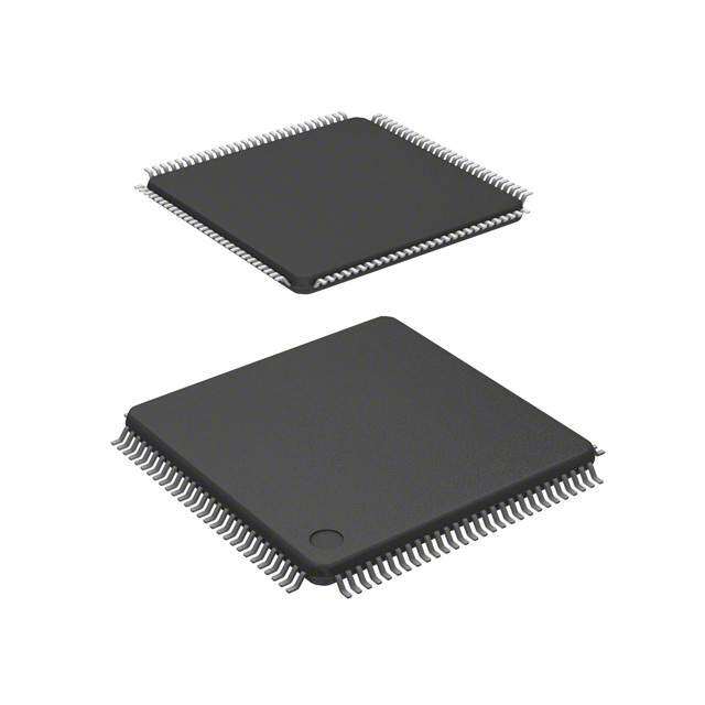
| 供应商器件封装 | 20-PDIP |
| 其它名称 | 296-33464-5 |
| 制造商产品页 | http://www.ti.com/general/docs/suppproductinfo.tsp?distId=10&orderablePartNumber=MSP430G2533IN20 |
| 包装 | 管件 |
| 可用A/D通道 | 8 Channel |
| 可编程输入/输出端数量 | 16 |
| 商标 | Texas Instruments |
| 商标名 | MSP430 |
| 处理器系列 | 2 Series |
| 外设 | 欠压检测/复位,PWM,WDT |
| 安装风格 | Through Hole |
| 定时器数量 | 2 Timer |
| 封装/外壳 | 20-DIP(0.300",7.62mm) |
| 封装/箱体 | PDIP-20 |
| 工作温度 | -40°C ~ 85°C |
| 工作电源电压 | 1.8 V to 3.6 V |
| 工厂包装数量 | 20 |
| 振荡器类型 | 内部 |
| 接口类型 | I2C, IrDA, SPI, UART |
| 数据RAM大小 | 512 B |
| 数据Ram类型 | SRAM |
| 数据总线宽度 | 16 bit |
| 数据转换器 | A/D 8x10b |
| 最大工作温度 | + 85 C |
| 最大时钟频率 | 16 MHz |
| 最小工作温度 | - 40 C |
| 标准包装 | 20 |
| 核心 | MSP430 |
| 核心处理器 | MSP430 |
| 核心尺寸 | 16-位 |
| 片上ADC | Yes |
| 电压-电源(Vcc/Vdd) | 1.8 V ~ 3.6 V |
| 程序存储器大小 | 16 kB |
| 程序存储器类型 | Flash |
| 程序存储容量 | 16KB(16K x 8) |
| 系列 | MSP430G2533 |
| 输入/输出端数量 | 16 I/O |
| 连接性 | I²C, IrDA, LIN, SCI, SPI, UART/USART |
| 速度 | 16MHz |


PDF Datasheet 数据手册内容提取
Product Sample & Technical Tools & Support & Reference Folder Buy Documents Software Community Design MSP430G2533,MSP430G2433,MSP430G2333,MSP430G2233 MSP430G2403,MSP430G2303,MSP430G2203 SLAS734G–APRIL2011–REVISEDAPRIL2016 MSP430G2x33, MSP430G2x03 Mixed-Signal Microcontrollers 1 Device Overview 1.1 Features 1 • LowSupply-VoltageRange:1.8Vto3.6V • UniversalSerialCommunicationInterface(USCI) • Ultra-LowPowerConsumption – EnhancedUARTSupportsAutomaticBaud- – ActiveMode:230 µAat1MHz,2.2V RateDetection(LIN) – StandbyMode:0.5 µA – IrDAEncoderandDecoder – OffMode(RAMRetention):0.1 µA – SynchronousSPI • FivePower-SavingModes – I2C • Ultra-FastWakeupFromStandbyModeinLess • 10-Bit200-kspsAnalog-to-DigitalConverter(ADC) Than1µs WithInternalReference,Sample-and-Hold,and Autoscan(SeeTable3-1) • 16-BitRISCArchitecture,62.5-nsInstructionCycle Time • BrownoutDetector • BasicClockModuleConfigurations • SerialOnboardProgramming, NoExternalProgrammingVoltageNeeded, – InternalFrequenciesupto16MHzWithFour ProgrammableCodeProtectionbySecurityFuse CalibratedFrequencies • On-ChipEmulationLogicWithSpy-Bi-Wire – InternalVery-Low-PowerLow-Frequency(LF) Interface Oscillator • Section3 SummarizesAvailableFamilyMembers – 32-kHzCrystal • PackageOptions – ExternalDigitalClockSource – TSSOP:20Pin,28Pin • Two16-BitTimer_AWithThreeCapture/Compare Registers – PDIP:20Pin • Upto24Capacitive-TouchEnabledI/OPins – QFN:32Pin • ForCompleteModuleDescriptions,Seethe MSP430x2xxFamilyUser’sGuide(SLAU144) 1.2 Applications • PowerManagement • CapacitiveTouch • SensorInterface 1.3 Description The TI MSP family of ultra-low-power microcontrollers consists of several devices that feature different sets of peripherals targeted for various applications. The architecture, combined with five low-power modes, is optimized to achieve extended battery life in portable measurement applications. The device features a powerful 16-bit RISC CPU, 16-bit registers, and constant generators that contribute to maximum code efficiency. The digitally controlled oscillator (DCO) allows the device to wake up from low- powermodestoactivemodeinlessthan1µs. The MSP430G2x03 and MSP430G2x33 devices are ultra-low-power mixed-signal microcontrollers with built-in 16-bit timers, up to 24 I/O capacitive-touch enabled pins, and built-in communication capability using the USCI. In addition, the MSP430G2x33 family members have a 10-bit ADC. See Section 3 for configurationdetails. Typical applications include low-cost sensor systems that capture analog signals, convert them to digital values,andthenprocessthedatafordisplayorfortransmissiontoahostsystem. 1 An IMPORTANT NOTICE at the end of this data sheet addresses availability, warranty, changes, use in safety-critical applications, intellectualpropertymattersandotherimportantdisclaimers.PRODUCTIONDATA.
MSP430G2533,MSP430G2433,MSP430G2333,MSP430G2233 MSP430G2403,MSP430G2303,MSP430G2203 SLAS734G–APRIL2011–REVISEDAPRIL2016 www.ti.com DeviceInformation(1) PARTNUMBER PACKAGE BODYSIZE(2) MSP430G2533IRHB VQFN(32) 5mm×5mm TSSOP(28) 9.7mm×4.4mm MSP430G2533IPW TSSOP(20) 6.5mm×4.4mm MSP430G2533IN PDIP(20) 24.33mm×6.35mm (1) Forthemostcurrentpart,package,andorderinginformation,seethePackageOptionAddendumin Section8,orseetheTIwebsiteatwww.ti.com. (2) Thesizesshownhereareapproximations.Forthepackagedimensionswithtolerances,seethe MechanicalDatainSection8. 1.4 Functional Block Diagrams Figure1-1showsthefunctionalblockdiagramoftheMSP430G2x33MCUs. XIN XOUT DVCC DVSS P1.x P2.x P3.x 8 8 8 ACLK Flash RAM ADC Port P1 Port P2 Port P3 Clock System SMCLK 16KB 512B 10 bit, 8 I/Os, 8 I/Os, 8 I/Os, 8KB 256B 8 channel, interrupt interrupt pullup or 4KB autoscan, capability, capability, pulldown MCLK 2KB 1-channel pullup or pullup or resistors DMA pulldown pulldown resistors resistors 16-MHz MAB CPU including MDB 16 registers Emulation Brownout Watchdog Timer0_A3 Timer1_A3 USCIA0 2BP Protection WDT+ UART, 3 CC 3 CC LIN, IrDA, 15-Bit registers registers SPI JTAG interface USCI B0 SPI, I2C Spy-Bi- Wire RST/NMI Copyright © 2016,Texas Instruments Incorporated NOTE: PortP3isavailableon28-pinand32-pindevicesonly. Figure1-1.FunctionalBlockDiagram,MSP430G2x33 2 DeviceOverview Copyright©2011–2016,TexasInstrumentsIncorporated SubmitDocumentationFeedback ProductFolderLinks:MSP430G2533 MSP430G2433 MSP430G2333 MSP430G2233MSP430G2403 MSP430G2303 MSP430G2203
MSP430G2533,MSP430G2433,MSP430G2333,MSP430G2233 MSP430G2403,MSP430G2303,MSP430G2203 www.ti.com SLAS734G–APRIL2011–REVISEDAPRIL2016 Figure1-2showsthefunctionalblockdiagramoftheMSP430G2x03MCUs. XIN XOUT DVCC DVSS P1.x P2.x P3.x 8 8 8 ACLK Flash RAM Port P1 Port P2 Port P3 Clock System SMCLK 8KB 256B 8 I/Os, 8 I/Os, 8 I/Os, 4KB interrupt interrupt pullup or 2KB capability, capability, pulldown MCLK pullup or pullup or resistors pulldown pulldown resistors resistors 16-MHz MAB CPU including MDB 16 registers Emulation Brownout Watchdog Timer0_A3 Timer1_A3 USCIA0 2BP Protection WDT+ UART, 3 CC 3 CC LIN, IrDA, 15-Bit registers registers SPI JTAG interface USCI B0 SPI, I2C Spy-Bi- Wire RST/NMI Copyright © 2016,Texas Instruments Incorporated NOTE: PortP3isavailableon28-pinand32-pindevicesonly. Figure1-2.FunctionalBlockDiagram,MSP430G2x03 Copyright©2011–2016,TexasInstrumentsIncorporated DeviceOverview 3 SubmitDocumentationFeedback ProductFolderLinks:MSP430G2533 MSP430G2433 MSP430G2333 MSP430G2233MSP430G2403 MSP430G2303 MSP430G2203
MSP430G2533,MSP430G2433,MSP430G2333,MSP430G2233 MSP430G2403,MSP430G2303,MSP430G2203 SLAS734G–APRIL2011–REVISEDAPRIL2016 www.ti.com Table of Contents 1 DeviceOverview......................................... 1 5.25 USCI(UARTMode)................................. 28 .............................................. ............................ 1.1 Features 1 5.26 USCI(SPIMasterMode) 28 ........................................... ............................. 1.2 Applications 1 5.27 USCI(SPISlaveMode) 29 1.3 Description............................................ 1 5.28 USCI(I2CMode).................................... 30 1.4 FunctionalBlockDiagrams........................... 2 5.29 10-BitADC,PowerSupplyandInputRange ................... 2 Revision History......................................... 5 Conditions(MSP430G2x33Only) 31 3 DeviceComparison ..................................... 6 5.30 10-BitADC,Built-InVoltageReference ............................... (MSP430G2x33 Only) 32 ..................................... 3.1 RelatedProducts 7 5.31 10-BitADC,ExternalReference(MSP430G2x33 4 TerminalConfigurationandFunctions.............. 8 Only)................................................. 33 ......................................... 4.1 PinDiagrams 8 5.32 10-BitADC,TimingParameters(MSP430G2x33 4.2 SignalDescriptions.................................. 10 Only)................................................. 33 5 Specifications........................................... 13 5.33 10-BitADC,LinearityParameters(MSP430G2x33 ................................................. ........................ Only) 33 5.1 AbsoluteMaximumRatings 13 5.2 ESDRatings........................................ 13 5.34 10-BitADC,Temperatu..re...S.e.n..s.o.r..a.n..d..B.u..il.t-.I.n..V.M..ID.. (MSP430G2x33 Only) 34 ............... 5.3 RecommendedOperatingConditions 13 ....................................... 5.35 FlashMemory 34 5.4 ActiveModeSup.p.l.y..C.u..r.re..n.t.I.n.t.o..V..C.C..E..x.c.l.u.d.i.n.g..... 5.36 RAM................................................. 35 External Current 14 .................... 5.37 JTAGandSpy-Bi-WireInterface 35 5.5 TypicalCharacteristics,ActiveModeSupplyCurrent (IntoV )............................................ 15 5.38 JTAGFuse.......................................... 35 CC 5.6 Low-PowerModeSupplyCurrents(IntoV ) 6 DetailedDescription................................... 36 CC ExcludingExternalCurrent.......................... 16 6.1 CPU................................................. 36 5.7 TypicalCharacteristics,Low-PowerModeSupply ....................................... 6.2 InstructionSet 37 ............................................. Currents 17 .................................... 6.3 OperatingModes 38 ................ 5.8 ThermalResistanceCharacteristics 18 .......................... 6.4 InterruptVectorAddresses 39 .................... 5.9 Schmitt-TriggerInputs,PortsPx 19 ................. 6.5 SpecialFunctionRegisters(SFRs) 40 .......................... 5.10 LeakageCurrent,PortsPx 19 ............................... 6.6 Memory Organization 41 ................................... 5.11 Outputs,PortsPx 19 .................................... 6.7 Bootloader(BSL) 41 ........................ 5.12 OutputFrequency,PortsPx 19 ....................................... 6.8 FlashMemory 42 ................... 5.13 TypicalCharacteristics–Outputs 20 .......................................... 6.9 Peripherals 42 ................ 5.14 Pin-OscillatorFrequency–PortsPx 21 ................................... 6.10 I/OPortDiagrams 48 . 5.15 TypicalCharacteristics–Pin-OscillatorFrequency 21 7 DeviceandDocumentationSupport............... 64 .......................................... 5.16 POR, BOR 22 ..................... 7.1 GettingStartedandNextSteps 64 .......................... 5.17 MainDCOCharacteristics 24 ............................... 7.2 Device Nomenclature 64 ..................................... 5.18 DCO Frequency 24 ................................. 7.3 ToolsandSoftware 66 ........... 5.19 CalibratedDCOFrequencies,Tolerance 25 ............................. 7.4 DocumentationSupport 68 5.20 Wake-upTimesFromLower-PowerModes(LPM3, ........................................ .............................................. 7.5 RelatedLinks 70 LPM4) 26 .............................. 5.21 TypicalCharacteristics,DCOClockWake-upTime 7.6 CommunityResources 71 ................................ .......................................... FromLPM3orLPM4 26 7.7 Trademarks 71 ..... ..................... 5.22 CrystalOscillator,XT1,Low-FrequencyMode 27 7.8 ElectrostaticDischargeCaution 71 5.23 InternalVery-Low-PowerLow-FrequencyOscillator 7.9 Glossary............................................. 71 ................................................ (VLO) 27 8 Mechanical,Packaging,andOrderable 5.24 Timer_A............................................. 27 Information.............................................. 72 4 TableofContents Copyright©2011–2016,TexasInstrumentsIncorporated SubmitDocumentationFeedback ProductFolderLinks:MSP430G2533 MSP430G2433 MSP430G2333 MSP430G2233MSP430G2403 MSP430G2303 MSP430G2203
MSP430G2533,MSP430G2433,MSP430G2333,MSP430G2233 MSP430G2403,MSP430G2303,MSP430G2203 www.ti.com SLAS734G–APRIL2011–REVISEDAPRIL2016 2 Revision History NOTE:Pagenumbersforpreviousrevisionsmaydifferfrompagenumbersinthecurrentversion. ChangesfromMay2,2013toApril27,2016 Page • Documentformatandorganizationchangesthroughout,includingadditionofsectionnumbering........................ 1 • AddedDeviceInformationtable .................................................................................................... 2 • AddedSection3.1,RelatedProducts ............................................................................................. 7 • MovedSection5,Specifications.................................................................................................. 13 • AddedSection5.2,ESDRatings.................................................................................................. 13 • AddedSection5.8,ThermalResistanceCharacteristics...................................................................... 18 • Throughoutdocument,changedallinstancesof"bootstraploader"to"bootloader"....................................... 39 • Changedallinstancesof"INCHx=0x1010"to"INCHx=1010b"inTable6-11,LabelsUsedbytheADC CalibrationTags..................................................................................................................... 43 • MovedandrenamedSection6.10,I/OPortDiagrams......................................................................... 48 • AddednotestoUCB0STEandUCA0CLKinTable6-18...................................................................... 53 • AddednotestoUCB0CLKandUCA0STEinTable6-19...................................................................... 55 • Added"andPW28"totitleofSection6.10.8.................................................................................... 62 • Added"andPW28"totitleofTable6-23......................................................................................... 63 • AddedSection7,DeviceandDocumentationSupport......................................................................... 64 • AddedSection8,Mechanical,Packaging,andOrderableInformation...................................................... 72 Copyright©2011–2016,TexasInstrumentsIncorporated RevisionHistory 5 SubmitDocumentationFeedback ProductFolderLinks:MSP430G2533 MSP430G2433 MSP430G2333 MSP430G2233MSP430G2403 MSP430G2303 MSP430G2203
MSP430G2533,MSP430G2433,MSP430G2333,MSP430G2233 MSP430G2403,MSP430G2303,MSP430G2203 SLAS734G–APRIL2011–REVISEDAPRIL2016 www.ti.com 3 Device Comparison Table3-1comparestheavailablefamilymembers. Table3-1.DeviceComparison(1)(2) FLASH RAM ADC10 USCI_A0, DEVICE BSL EEM Timer_A CLOCK I/O PACKAGE (KB) (B) CHANNELS USCI_B0 24 32-QFN LF,DCO, 24 28-TSSOP MSP430G2533 1 1 16 512 2xTA3 8 1 VLO 16 20-TSSOP 16 20-PDIP 24 32-QFN LF,DCO, 24 28-TSSOP MSP430G2433 1 1 8 512 2xTA3 8 1 VLO 16 20-TSSOP 16 20-PDIP 24 32-QFN LF,DCO, 24 28-TSSOP MSP430G2333 1 1 4 256 2xTA3 8 1 VLO 16 20-TSSOP 16 20-PDIP 24 32-QFN LF,DCO, 24 28-TSSOP MSP430G2233 1 1 2 256 2xTA3 8 1 VLO 16 20-TSSOP 16 20-PDIP 24 32-QFN LF,DCO, 24 28-TSSOP MSP430G2403 1 1 8 512 2xTA3 – 1 VLO 16 20-TSSOP 16 20-PDIP 24 32-QFN LF,DCO, 24 28-TSSOP MSP430G2303 1 1 4 256 2xTA3 – 1 VLO 16 20-TSSOP 16 20-PDIP 24 32-QFN LF,DCO, 24 28-TSSOP MSP430G2203 1 1 2 256 2xTA3 – 1 VLO 16 20-TSSOP 16 20-PDIP (1) Forthemostcurrentdevice,package,andorderinginformation,seethePackageOptionAddenduminSection8,orseetheTIwebsite atwww.ti.com. (2) Packagedrawings,thermaldata,andsymbolizationareavailableatwww.ti.com/packaging. 6 DeviceComparison Copyright©2011–2016,TexasInstrumentsIncorporated SubmitDocumentationFeedback ProductFolderLinks:MSP430G2533 MSP430G2433 MSP430G2333 MSP430G2233MSP430G2403 MSP430G2303 MSP430G2203
MSP430G2533,MSP430G2433,MSP430G2333,MSP430G2233 MSP430G2403,MSP430G2303,MSP430G2203 www.ti.com SLAS734G–APRIL2011–REVISEDAPRIL2016 3.1 Related Products Forinformationaboutotherdevicesinthisfamilyofproductsorrelatedproducts,seethefollowinglinks. ProductsforMSP16-Bitand32-BitMCUs Low-power mixed-signal processors with smart analog and digitalperipheralsforawiderangeofindustrialandconsumerapplications. ProductsforUltra-lowPowerMCUs MSP Ultra-Low-Power microcontrollers (MCUs) from Texas Instruments (TI) offer the lowest power consumption and the perfect mix of integrated peripheralsforawiderangeoflow-powerandportableapplications. ProductsforMSP430G2x/i2xLow-CostIndustrialMCUs MSP430G2x microcontrollers (MCUs) from the MSP ultra-low-power MCU series, offers the low power and performance of 16-bit MSP microcontrollerswithafeaturesettargetedatcostsensitiveapplications. CompanionProductsforMSP430G2533 Review products that are frequently purchased or used in conjunctionwiththisproduct. ReferenceDesignsforMSP430G2533 TI Designs Reference Design Library is a robust reference design library that spans analog, embedded processor, and connectivity. Created by TI experts to help you jump start your system design, all TI Designs include schematic or block diagrams, BOMs, and design files to speed your time to market. Search and download designsat ti.com/tidesigns. Copyright©2011–2016,TexasInstrumentsIncorporated DeviceComparison 7 SubmitDocumentationFeedback ProductFolderLinks:MSP430G2533 MSP430G2433 MSP430G2333 MSP430G2233MSP430G2403 MSP430G2303 MSP430G2203
MSP430G2533,MSP430G2433,MSP430G2333,MSP430G2233 MSP430G2403,MSP430G2303,MSP430G2203 SLAS734G–APRIL2011–REVISEDAPRIL2016 www.ti.com 4 Terminal Configuration and Functions 4.1 Pin Diagrams Figure 4-1 shows the pinout for the MSP430G2x03 and MSP430G2x33 devices in the 20-pin N or PW package. DVCC 1 20 DVSS P1.0/TA0CLK/ACLK/A0 2 19 XIN/P2.6/TA0.1 P1.1/TA0.0/ U C A 0 R X D / U C A 0 S O M I / A1 3 18 XOUT/P2.7 P1.2/TA0.1/UCA0TXD/UCA0SIMO/A2 4 17 TEST/SBWTCK N20 P1.3/ADC10CLK/VREF-/VEREF-/A3 5 16 RST/NMI/SBWTDIO PW20 P1.4/SMCLK/UCB0STE/UCA0CLK/VREF+/VEREF+/A4/TCK 6 (TOPVIEW) 15 P1.7/UCB0SIMO/UCB0SDA/A7/TDO/TDI P1.5/TA0.0/UCB0CLK/UCA0STE/A5/TMS 7 14 P1.6/TA0.1/UCB0SOMI/UCB0SCL/A6/TDI/TCLK P2.0/TA1.0 8 13 P2.5/TA1.2 P2.1/TA1.1 9 12 P2.4/TA1.2 P2.2/TA1.1 10 11 P2.3/TA1.0 NOTE: ADC10isavailableonMSP430G2x33devicesonly. NOTE: ThepulldownresistorsofportP3shouldbeenabledbysettingP3REN.x=1. Figure4-1.20-PinNorPWPackage(TopView),MSP430G2x03andMSP430G2x33 Figure 4-2 shows the pinout for the MSP430G2x03 and MSP430G2x33 devices in the 28-pin PW package. DVCC 1 28 DVSS P1.0/TA0CLK/ACLK/A0 2 27 XIN/P2.6/TA0.1 P1.1/TA0.0/ U C A 0 R X D / U C A 0 S O M I / A1 3 26 XOUT/P2.7 P1.2/TA0.1/UCA0TXD/UCA0SIMO/A2 4 25 TEST/SBWTCK P1.3/ADC10CLK/VREF-/VEREF-/A3 5 24 RST/NMI/SBWTDIO P1.4/SMCLK/UCB0STE/UCA0CLK/VREF+/VEREF+/A4/TCK 6 23 P1.7/UCB0SIMO/UCB0SDA/A7/TDO/TDI P1.5/TA0.0/UCB0CLK/UCA0STE/A5/TMS 7 PW28 22 P1.6/TA0.1/UCB0SOMI/UCB0SCL/A6/TDI/TCLK (TOPVIEW) P3.1/TA1.0 8 21 P3.7/TA1CLK P3.0/TA0.2 9 20 P3.6/TA0.2 P2.0/TA1.0 10 19 P3.5/TA0.1 P2.1/TA1.1 11 18 P2.5/TA1.2 P2.2/TA1.1 12 17 P2.4/TA1.2 P3.2/TA1.1 13 16 P2.3/TA1.0 P3.3/TA1.2 14 15 P3.4/TA0.0 NOTE: ADC10isavailableonMSP430G2x33devicesonly. Figure4-2.28-PinPWPackage(TopView),MSP430G2x03andMSP430G2x33 8 TerminalConfigurationandFunctions Copyright©2011–2016,TexasInstrumentsIncorporated SubmitDocumentationFeedback ProductFolderLinks:MSP430G2533 MSP430G2433 MSP430G2333 MSP430G2233MSP430G2403 MSP430G2303 MSP430G2203
MSP430G2533,MSP430G2433,MSP430G2333,MSP430G2233 MSP430G2403,MSP430G2303,MSP430G2203 www.ti.com SLAS734G–APRIL2011–REVISEDAPRIL2016 Figure 4-3 shows the pinout for the MSP430G2x03 and MSP430G2x33 devices in the 32-pin RHB package. 0 A C 0/ A K/ L C A 1 K/ 0. NC P1.0/TA0CL DVCC AVCC DVSS AVSS XIN/P2.6/TA XOUT/P2.7 32 31 30 29 28 27 26 25 P1.1/TA0.0/ U C A 0 R X D / U C A 0 S O M I / A1 1 24 TEST/SBWTCK P1.2/TA0.1/UCA0TXD/UCA0SIMO/A2 2 23 RST/NMI/SBWTDIO P1.3/ADC10CLK/VREF-/VEREF-/A3 3 22 P1.7/UCB0SIMO/UCB0SDA/A7/TDO/TDI P1.4/SMCLK/UCB0STE/UCA0CLK/VREF+/VEREF+/A4/TCK 4 RHB32 21 P1.6/TA0.1/UCB0SOMI/UCB0SCL/A6/TDI/TCLK P1.5/TA0.0/UCB0CLK/UCA0STE/A5/TMS 5 (TOPVIEW) 20 P3.7/TA1CLK P3.1/TA1.0 6 19 P3.6/TA0.2 P3.0/TA0.2 7 18 P3.5/TA0.1 NC 8 17 P2.5/TA1.2 9 10 11 12 13 14 15 16 0 1 1 1 2 0 0 2 1. 1. 1. 1. 1. 0. 1. 1. A A A A A A A A T T T T T T T T 0/ 1/ 2/ 2/ 3/ 4/ 3/ 4/ 2. 2. 2. 3. 3. 3. 2. 2. P P P P P P P P NOTE: ADC10isavailableonMSP430G2x33devicesonly. Figure4-3.32-PinRHBPackage(TopView),MSP430G2x03andMSP430G2x33 Copyright©2011–2016,TexasInstrumentsIncorporated TerminalConfigurationandFunctions 9 SubmitDocumentationFeedback ProductFolderLinks:MSP430G2533 MSP430G2433 MSP430G2333 MSP430G2233MSP430G2403 MSP430G2303 MSP430G2203
MSP430G2533,MSP430G2433,MSP430G2333,MSP430G2233 MSP430G2403,MSP430G2303,MSP430G2203 SLAS734G–APRIL2011–REVISEDAPRIL2016 www.ti.com 4.2 Signal Descriptions Table4-1describesthesignals. Table4-1.TerminalFunctions TERMINAL NO. I/O DESCRIPTION NAME PW20, PW28 RHB32 N20 P1.0/ General-purposedigitalI/Opin TA0CLK/ Timer0_A,clocksignalTACLKinput 2 2 31 I/O ACLK/ ACLKsignaloutput A0 ADC10analoginputA0(1) P1.1/ General-purposedigitalI/Opin TA0.0/ Timer0_A,capture:CCI0Ainput,compare:Out0output/BSLtransmit UCA0RXD/ 3 3 1 I/O USCI_A0receivedatainputinUARTmode UCA0SOMI/ USCI_A0slavedataout/masterinSPImode A1 ADC10analoginputA1(1) P1.2/ General-purposedigitalI/Opin TA0.1/ Timer0_A,capture:CCI1Ainput,compare:Out1output UCA0TXD/ 4 4 2 I/O USCI_A0transmitdataoutputinUARTmode UCA0SIMO/ USCI_A0slavedatain/masteroutinSPImode A2 ADC10analoginputA2(1) P1.3/ General-purposedigitalI/Opin ADC10CLK/ ADC10,conversionclockoutput(1) 5 5 3 I/O A3/ ADC10analoginputA3(1) VREF-/VEREF- ADC10negativereferencevoltage (1) P1.4/ General-purposedigitalI/Opin SMCLK/ SMCLKsignaloutput UCB0STE/ USCI_B0slavetransmitenable UCA0CLK/ 6 6 4 I/O USCI_A0clockinput/output A4/ ADC10analoginputA4(1) VREF+/VEREF+ ADC10positivereferencevoltage(1) TCK JTAGtestclock,inputterminalfordeviceprogrammingandtest P1.5/ General-purposedigitalI/Opin TA0.0/ Timer0_A,compare:Out0output/BSLreceive UCB0CLK/ USCI_B0clockinput/output 7 7 5 I/O UCA0STE/ USCI_A0slavetransmitenable A5/ ADC10analoginputA5(1) TMS JTAGtestmodeselect,inputterminalfordeviceprogrammingandtest P1.6/ General-purposedigitalI/Opin TA0.1/ Timer0_A,compare:Out1output A6/ ADC10analoginputA6(1) 14 22 21 I/O UCB0SOMI/ USCI_B0slaveout/masterinSPImode, UCB0SCL/ USCI_B0SCLI2CclockinI2Cmode TDI/TCLK JTAGtestdatainputortestclockinputduringprogrammingandtest (1) MSP430G2x33devicesonly 10 TerminalConfigurationandFunctions Copyright©2011–2016,TexasInstrumentsIncorporated SubmitDocumentationFeedback ProductFolderLinks:MSP430G2533 MSP430G2433 MSP430G2333 MSP430G2233MSP430G2403 MSP430G2303 MSP430G2203
MSP430G2533,MSP430G2433,MSP430G2333,MSP430G2233 MSP430G2403,MSP430G2303,MSP430G2203 www.ti.com SLAS734G–APRIL2011–REVISEDAPRIL2016 Table4-1.TerminalFunctions(continued) TERMINAL NO. I/O DESCRIPTION NAME PW20, PW28 RHB32 N20 P1.7/ General-purposedigitalI/Opin A7/ ADC10analoginputA7(1) UCB0SIMO/ USCI_B0slavein/masteroutinSPImode 15 23 22 I/O UCB0SDA/ USCI_B0SDAI2CdatainI2Cmode JTAGtestdataoutputterminalortestdatainputduringprogrammingand TDO/TDI test(2) P2.0/ General-purposedigitalI/Opin 8 10 9 I/O TA1.0 Timer1_A,capture:CCI0Ainput,compare:Out0output P2.1/ General-purposedigitalI/Opin 9 11 10 I/O TA1.1 Timer1_A,capture:CCI1Ainput,compare:Out1output P2.2/ General-purposedigitalI/Opin 10 12 11 I/O TA1.1 Timer1_A,capture:CCI1Binput,compare:Out1output P2.3/ General-purposedigitalI/Opin 11 16 15 I/O TA1.0 Timer1_A,capture:CCI0Binput,compare:Out0output P2.4/ General-purposedigitalI/Opin 12 17 16 I/O TA1.2 Timer1_A,capture:CCI2Ainput,compare:Out2output P2.5/ General-purposedigitalI/Opin 13 18 17 I/O TA1.2 Timer1_A,capture:CCI2Binput,compare:Out2output XIN/ Inputterminalofcrystaloscillator P2.6/ 19 27 26 I/O General-purposedigitalI/Opin TA0.1 Timer0_A,compare:Out1output XOUT/ Outputterminalofcrystaloscillator(3) 18 26 25 I/O P2.7 General-purposedigitalI/Opin P3.0/ General-purposedigitalI/Opin - 9 7 I/O TA0.2 Timer0_A,capture:CCI2Ainput,compare:Out2output P3.1/ General-purposedigitalI/Opin - 8 6 I/O TA1.0 Timer1_A,compare:Out0output P3.2/ General-purposedigitalI/Opin - 13 12 I/O TA1.1 Timer1_A,compare:Out1output P3.3/ General-purposedigitalI/O - 14 13 I/O TA1.2 Timer1_A,compare:Out2output P3.4/ General-purposedigitalI/O - 15 14 I/O TA0.0 Timer0_A,compare:Out0output P3.5/ General-purposedigitalI/O - 19 18 I/O TA0.1 Timer0_A,compare:Out1output P3.6/ General-purposedigitalI/O - 20 19 I/O TA0.2 Timer0_A,compare:Out2output P3.7/ General-purposedigitalI/O - 21 20 I/O TA1CLK Timer1_A,clocksignalTACLKinput RST/ Reset NMI/ 16 24 23 I Nonmaskableinterruptinput SBWTDIO Spy-Bi-Wiretestdatainput/outputduringprogrammingandtest (2) TDOorTDIisselectedbyJTAGinstruction. (3) IfXOUT/P2.7isusedasaninput,excesscurrentflowsuntilP2SEL.7iscleared.Thisisduetotheoscillatoroutputdriverconnectionto thispadafterreset. Copyright©2011–2016,TexasInstrumentsIncorporated TerminalConfigurationandFunctions 11 SubmitDocumentationFeedback ProductFolderLinks:MSP430G2533 MSP430G2433 MSP430G2333 MSP430G2233MSP430G2403 MSP430G2303 MSP430G2203
MSP430G2533,MSP430G2433,MSP430G2333,MSP430G2233 MSP430G2403,MSP430G2303,MSP430G2203 SLAS734G–APRIL2011–REVISEDAPRIL2016 www.ti.com Table4-1.TerminalFunctions(continued) TERMINAL NO. I/O DESCRIPTION NAME PW20, PW28 RHB32 N20 SelectstestmodeforJTAGpinsonPort1.Thedeviceprotectionfuseis TEST/ 17 25 24 I connectedtoTEST. SBWTCK Spy-Bi-Wiretestclockinputduringprogrammingandtest AVCC NA NA 29 NA Analogsupplyvoltage DVCC 1 1 30 NA Digitalsupplyvoltage DVSS 20 28 27,28 NA Groundreference NC NA NA 8,32 NA Notconnected QFNPad NA NA Pad NA QFNpackagepadconnectiontoVSSrecommended. 12 TerminalConfigurationandFunctions Copyright©2011–2016,TexasInstrumentsIncorporated SubmitDocumentationFeedback ProductFolderLinks:MSP430G2533 MSP430G2433 MSP430G2333 MSP430G2233MSP430G2403 MSP430G2303 MSP430G2203
MSP430G2533,MSP430G2433,MSP430G2333,MSP430G2233 MSP430G2403,MSP430G2303,MSP430G2203 www.ti.com SLAS734G–APRIL2011–REVISEDAPRIL2016 5 Specifications 5.1 Absolute Maximum Ratings(1) overoperatingfree-airtemperaturerange(unlessotherwisenoted) MIN MAX UNIT VoltageappliedatV toV –0.3 4.1 V CC SS Voltageappliedtoanypin(2) –0.3 V +0.3 V CC Diodecurrentatanydevicepin ±2 mA Unprogrammeddevice –55 150 Storagetemperature,T (3) °C stg Programmeddevice –55 150 (1) StressesbeyondthoselistedunderAbsoluteMaximumRatingsmaycausepermanentdamagetothedevice.Thesearestressratings only,andfunctionaloperationofthedeviceattheseoranyotherconditionsbeyondthoseindicatedunderRecommendedOperating Conditionsisnotimplied.Exposuretoabsolute-maximum-ratedconditionsforextendedperiodsmayaffectdevicereliability. (2) AllvoltagesreferencedtoV .TheJTAGfuse-blowvoltage,V ,isallowedtoexceedtheabsolutemaximumrating.Thevoltageis SS FB appliedtotheTESTpinwhenblowingtheJTAGfuse. (3) HighertemperaturemaybeappliedduringboardsolderingaccordingtothecurrentJEDECJ-STD-020specificationwithpeakreflow temperaturesnothigherthanclassifiedonthedevicelabelontheshippingboxesorreels. 5.2 ESD Ratings VALUE UNIT Human-bodymodel(HBM),perANSI/ESDA/JEDECJS-001(1) ±1000 V Electrostaticdischarge V (ESD) Charged-devicemodel(CDM),perJEDECspecificationJESD22-C101(2) ±250 (1) JEDECdocumentJEP155statesthat500-VHBMallowssafemanufacturingwithastandardESDcontrolprocess.Pinslistedas ±1000Vmayactuallyhavehigherperformance. (2) JEDECdocumentJEP157statesthat250-VCDMallowssafemanufacturingwithastandardESDcontrolprocess.Pinslistedas±250V mayactuallyhavehigherperformance. 5.3 Recommended Operating Conditions TypicalvaluesarespecifiedatV =3.3VandT =25°C(unlessotherwisenoted) CC A MIN NOM MAX UNIT Duringprogramexecution 1.8 3.6 V Supplyvoltage V CC Duringflashprogrammingorerase 2.2 3.6 V Supplyvoltage 0 V SS T Operatingfree-airtemperature –40 85 °C A V =1.8V, CC DC 6 Dutycycle=50%±10% Processorfrequency(maximumMCLKfrequency V =2.7V, fSYSTEM usingtheUSARTmodule)(1)(2) DCuCtycycle=50%±10% DC 12 MHz V =3.3V, CC DC 16 Dutycycle=50%±10% (1) TheMSP430CPUisclockeddirectlywithMCLK.BoththehighandlowphasesofMCLKmustnotexceedthepulsedurationofthe specifiedmaximumfrequency. (2) Modulesmighthaveadifferentmaximuminputclockspecification.Seethespecificationoftherespectivemoduleinthisdatasheet. Copyright©2011–2016,TexasInstrumentsIncorporated Specifications 13 SubmitDocumentationFeedback ProductFolderLinks:MSP430G2533 MSP430G2433 MSP430G2333 MSP430G2233MSP430G2403 MSP430G2303 MSP430G2203
MSP430G2533,MSP430G2433,MSP430G2333,MSP430G2233 MSP430G2403,MSP430G2303,MSP430G2203 SLAS734G–APRIL2011–REVISEDAPRIL2016 www.ti.com Legend: 16 MHz Supply voltage range, Hz during flash memory M programming y - 12 MHz c n e u Supply voltage range, q e during program execution Fr m ste 6 MHz y S 1.8 V 2.2 V 2.7 V 3.3 V 3.6 V Supply Voltage - V Note: Minimumprocessorfrequencyisdefinedbysystemclock.FlashprogramoreraseoperationsrequireaminimumV CC of2.2V. Figure5-1.SafeOperatingArea 5.4 Active Mode Supply Current Into V Excluding External Current CC overrecommendedrangesofsupplyvoltageandoperatingfree-airtemperature(unlessotherwisenoted)(1)(2) PARAMETER TESTCONDITIONS V MIN TYP MAX UNIT CC f =f =f =1MHz, 2.2V 230 DCO MCLK SMCLK f =0Hz, ACLK Programexecutesinflash, Activemode(AM) I BCSCTL1=CALBC1_1MHZ, µA AM,1MHz currentat1MHz DCOCTL=CALDCO_1MHZ, 3V 330 420 CPUOFF=0,SCG0=0,SCG1=0, OSCOFF=0 (1) Allinputsaretiedto0VortoV .Outputsdonotsourceorsinkanycurrent. CC (2) ThecurrentsarecharacterizedwithaMicroCrystalCC4V-T1ASMDcrystalwithaloadcapacitanceof9pF.Theinternalandexternal loadcapacitanceischosentocloselymatchtherequired9pF. 14 Specifications Copyright©2011–2016,TexasInstrumentsIncorporated SubmitDocumentationFeedback ProductFolderLinks:MSP430G2533 MSP430G2433 MSP430G2333 MSP430G2233MSP430G2403 MSP430G2303 MSP430G2203
MSP430G2533,MSP430G2433,MSP430G2333,MSP430G2233 MSP430G2403,MSP430G2303,MSP430G2203 www.ti.com SLAS734G–APRIL2011–REVISEDAPRIL2016 5.5 Typical Characteristics, Active Mode Supply Current (Into V ) CC 5.0 4.0 4.0 fDCO= 16 MHz TA= 85°C A A 3.0 m m − − TA= 25°C Active Mode Current 23..00 fDCO= 8 MfHDzCO= 12 MHz Active Mode Current 12..00 VCC= 3 V TTAA== 8255°°CC 1.0 fDCO= 1 MHz VCC= 2.2 V 0.0 0.0 1.5 2.0 2.5 3.0 3.5 4.0 0.0 4.0 8.0 12.0 16.0 VCC−Supply Voltage−V fDCO−DCO Frequency−MHz Figure5-2.ActiveModeCurrentvsV ,T =25°C Figure5-3.ActiveModeCurrentvsDCOFrequency CC A Copyright©2011–2016,TexasInstrumentsIncorporated Specifications 15 SubmitDocumentationFeedback ProductFolderLinks:MSP430G2533 MSP430G2433 MSP430G2333 MSP430G2233MSP430G2403 MSP430G2303 MSP430G2203
MSP430G2533,MSP430G2433,MSP430G2333,MSP430G2233 MSP430G2403,MSP430G2303,MSP430G2203 SLAS734G–APRIL2011–REVISEDAPRIL2016 www.ti.com 5.6 Low-Power Mode Supply Currents (Into V ) Excluding External Current CC overrecommendedrangesofsupplyvoltageandoperatingfree-airtemperature(unlessotherwisenoted)(1) (2) PARAMETER TESTCONDITIONS T V MIN TYP MAX UNIT A CC f =0MHz, MCLK f =f =1MHz, SMCLK DCO f =32768Hz, Low-powermode0 ACLK ILPM0,1MHz (LPM0)current(3) BCSCTL1=CALBC1_1MHZ, 25°C 2.2V 56 µA DCOCTL=CALDCO_1MHZ, CPUOFF=1,SCG0=0,SCG1=0, OSCOFF=0 f =f =0MHz, MCLK SMCLK f =1MHz, DCO f =32768Hz, Low-powermode2 ACLK ILPM2 (LPM2)current(4) BCSCTL1=CALBC1_1MHZ, 25°C 2.2V 22 µA DCOCTL=CALDCO_1MHZ, CPUOFF=1,SCG0=0,SCG1=1, OSCOFF=0 f =f =f =0MHz, DCO MCLK SMCLK Low-powermode3 f =32768Hz, ILPM3,LFXT1 (LPM3)current(4) CAPCLUKOFF=1,SCG0=1,SCG1=1, 25°C 2.2V 0.7 1.5 µA OSCOFF=0 f =f =f =0MHz, DCO MCLK SMCLK Low-powermode3 f frominternalLFoscillator(VLO), ILPM3,VLO current,(LPM3)(4) CAPCLUKOFF=1,SCG0=1,SCG1=1, 25°C 2.2V 0.5 0.7 µA OSCOFF=0 f =f =f =0MHz, 25°C 0.1 0.5 DCO MCLK SMCLK Low-powermode4 f =0Hz, ILPM4 (LPM4)current(5) CAPCLUKOFF=1,SCG0=1,SCG1=1, 85°C 2.2V 0.8 1.7 µA OSCOFF=1 (1) Allinputsaretiedto0VortoV .Outputsdonotsourceorsinkanycurrent. CC (2) ThecurrentsarecharacterizedwithaMicroCrystalCC4V-T1ASMDcrystalwithaloadcapacitanceof9pF.Theinternalandexternal loadcapacitanceischosentocloselymatchtherequired9pF. (3) CurrentforbrownoutandWDTclockedbySMCLKincluded. (4) CurrentforbrownoutandWDTclockedbyACLKincluded. (5) Currentforbrownoutincluded. 16 Specifications Copyright©2011–2016,TexasInstrumentsIncorporated SubmitDocumentationFeedback ProductFolderLinks:MSP430G2533 MSP430G2433 MSP430G2333 MSP430G2233MSP430G2403 MSP430G2303 MSP430G2203
MSP430G2533,MSP430G2433,MSP430G2333,MSP430G2233 MSP430G2403,MSP430G2303,MSP430G2203 www.ti.com SLAS734G–APRIL2011–REVISEDAPRIL2016 5.7 Typical Characteristics, Low-Power Mode Supply Currents overrecommendedrangesofsupplyvoltageandoperatingfree-airtemperature(unlessotherwisenoted) 3.00 2.50 2.75 2.25 A 2.50 A µ µ 2.00 Mode Current– 1122....57020505 Mode Current– 111...257505 w-Power 11..0205 VVCCCC== 3 3.6 V V w-Power 1.00 VVCCCC== 3 3.6 V V –Lo 0.75 VCC= 2.2 V –Lo 0.75 VCC= 2.2 V ILPM3 0.50 ILPM4 0.50 V = 1.8 V 0.25 0.25 CC V = 1.8 V 0.00 0.00 CC -40 -20 0 20 40 60 80 -40 -20 0 20 40 60 80 Figure5-4.LPM3TAC–uTrreemnptevrsatTureem–p°eCrature Figure5-5.LPM4TAC–uTrreemnptevrsatTureem–p°eCrature Copyright©2011–2016,TexasInstrumentsIncorporated Specifications 17 SubmitDocumentationFeedback ProductFolderLinks:MSP430G2533 MSP430G2433 MSP430G2333 MSP430G2233MSP430G2403 MSP430G2303 MSP430G2203
MSP430G2533,MSP430G2433,MSP430G2333,MSP430G2233 MSP430G2403,MSP430G2303,MSP430G2203 SLAS734G–APRIL2011–REVISEDAPRIL2016 www.ti.com 5.8 Thermal Resistance Characteristics PARAMETER VALUE (1) UNIT VQFN(RHB-32) 32.1 TSSOP(PW-28) 72.2 Rθ Junction-to-ambientthermalresistance,stillair (2) °C/W JA TSSOP(PW-20) 86.5 PDIP(N-20) 49.3 VQFN(RHB-32) 22.3 TSSOP(PW-28) 18.3 Rθ Junction-to-case(top)thermalresistance (3) °C/W JC(TOP) TSSOP(PW-20) 20.8 PDIP(N-20) 41 VQFN(RHB-32) 1.4 TSSOP(PW-28) N/A Rθ Junction-to-case(bottom)thermalresistance °C/W JC(BOTTOM) TSSOP(PW-20) N/A PDIP(N-20) N/A VQFN(RHB-32) 6.1 TSSOP(PW-28) 30.4 θ Junction-to-boardthermalresistance (4) °C/W JB TSSOP(PW-20) 39 PDIP(N-20) 30.2 VQFN(RHB-32) 0.3 TSSOP(PW-28) 0.7 Ψ Junction-to-package-topcharacterizationparameter °C/W JT TSSOP(PW-20) 0.8 PDIP(N-20) 18.1 VQFN(RHB-32) 6.1 TSSOP(PW-28) 29.9 Ψ Junction-to-boardcharacterizationparameter °C/W JB TSSOP(PW-20) 38.1 PDIP(N-20) 30.1 (1) ThesevaluesarebasedonaJEDEC-defined2S2Psystem(withtheexceptionoftheThetaJC(Rθ )value,whichisbasedona JC JEDEC-defined1S0Psystem)andwillchangebasedonenvironmentandapplication.Formoreinformation,seetheseEIA/JEDEC standards: • JESD51-2,IntegratedCircuitsThermalTestMethodEnvironmentalConditions-NaturalConvection(StillAir) • JESD51-3,LowEffectiveThermalConductivityTestBoardforLeadedSurfaceMountPackages • JESD51-7,HighEffectiveThermalConductivityTestBoardforLeadedSurfaceMountPackages • JESD51-9,TestBoardsforAreaArraySurfaceMountPackageThermalMeasurements (2) Thejunction-to-ambientthermalresistanceundernaturalconvectionisobtainedinasimulationonaJEDEC-standard,High-Kboard,as specifiedinJESD51-7,inanenvironmentdescribedinJESD51-2a. (3) Thejunction-to-case(top)thermalresistanceisobtainedbysimulatingacoldplatetestonthepackagetop.NospecificJEDEC- standardtestexists,butaclosedescriptioncanbefoundintheANSISEMIstandardG30-88. (4) Thejunction-to-boardthermalresistanceisobtainedbysimulatinginanenvironmentwitharingcoldplatefixturetocontrolthePCB temperature,asdescribedinJESD51-8. 18 Specifications Copyright©2011–2016,TexasInstrumentsIncorporated SubmitDocumentationFeedback ProductFolderLinks:MSP430G2533 MSP430G2433 MSP430G2333 MSP430G2233MSP430G2403 MSP430G2303 MSP430G2203
MSP430G2533,MSP430G2433,MSP430G2333,MSP430G2233 MSP430G2403,MSP430G2303,MSP430G2203 www.ti.com SLAS734G–APRIL2011–REVISEDAPRIL2016 5.9 Schmitt-Trigger Inputs, Ports Px overrecommendedrangesofsupplyvoltageandoperatingfree-airtemperature(unlessotherwisenoted) PARAMETER TESTCONDITIONS V MIN TYP MAX UNIT CC 0.45V 0.75V CC CC V Positive-goinginputthresholdvoltage V IT+ 3V 1.35 2.25 0.25V 0.55V CC CC V Negative-goinginputthresholdvoltage V IT– 3V 0.75 1.65 V Inputvoltagehysteresis(V –V ) 3V 0.3 1 V hys IT+ IT– Forpullup:V =V R Pulluporpulldownresistor IN SS 3V 20 35 50 kΩ Pull Forpulldown:V =V IN CC C Inputcapacitance V =V orV 5 pF I IN SS CC 5.10 Leakage Current, Ports Px overrecommendedrangesofsupplyvoltageandoperatingfree-airtemperature(unlessotherwisenoted) PARAMETER TESTCONDITIONS V MIN MAX UNIT CC I High-impedanceleakagecurrent See (1) (2) 3V ±50 nA lkg(Px.y) (1) TheleakagecurrentismeasuredwithV orV appliedtothecorrespondingpins,unlessotherwisenoted. SS CC (2) Theleakageofthedigitalportpinsismeasuredindividually.Theportpinisselectedforinputandthepullup/pulldownresistoris disabled. 5.11 Outputs, Ports Px overrecommendedrangesofsupplyvoltageandoperatingfree-airtemperature(unlessotherwisenoted) PARAMETER TESTCONDITIONS V MIN TYP MAX UNIT CC V High-leveloutputvoltage I =–6mA(1) 3V V –0.3 V OH (OHmax) CC V Low-leveloutputvoltage I =6mA(1) 3V V +0.3 V OL (OLmax) SS (1) Themaximumtotalcurrent,I andI ,foralloutputscombinedshouldnotexceed±48mAtoholdthemaximumvoltagedrop (OHmax) (OLmax) specified. 5.12 Output Frequency, Ports Px overrecommendedrangesofsupplyvoltageandoperatingfree-airtemperature(unlessotherwisenoted) PARAMETER TESTCONDITIONS V MIN TYP MAX UNIT CC f Portoutputfrequency(withload) Px.y,C =20pF,R =1kΩ(1) (2) 3V 12 MHz Px.y L L f Clockoutputfrequency Px.y,C =20pF(2) 3V 16 MHz Port_CLK L (1) Aresistivedividerwithtwo50-kΩresistorsbetweenV andV isusedasload.Theoutputisconnectedtothecentertapofthe CC SS divider. (2) Theoutputvoltagereachesatleast10%and90%V atthespecifiedtogglefrequency. CC Copyright©2011–2016,TexasInstrumentsIncorporated Specifications 19 SubmitDocumentationFeedback ProductFolderLinks:MSP430G2533 MSP430G2433 MSP430G2333 MSP430G2233MSP430G2403 MSP430G2303 MSP430G2203
MSP430G2533,MSP430G2433,MSP430G2333,MSP430G2233 MSP430G2403,MSP430G2303,MSP430G2203 SLAS734G–APRIL2011–REVISEDAPRIL2016 www.ti.com 5.13 Typical Characteristics – Outputs overrecommendedrangesofsupplyvoltageandoperatingfree-airtemperature(unlessotherwisenoted) 30 50 VCC= 2.2 V VCC= 3 V mA P1.7 TA= 25°C mA P1.7 TA= 25°C − 25 − 40 nt nt e e Curr 20 TA= 85°C Curr TA= 85°C put put 30 ut ut O O el 15 el v v e e w-L w-L 20 Lo 10 Lo al al c c Typi 5 Typi 10 − − OL OL I I 0 0 0 0.5 1 1.5 2 2.5 0 0.5 1 1.5 2 2.5 3 3.5 VOL−Low-Level Output Voltage−V VOL−Low-Level Output Voltage−V Figure5-6.TypicalLow-LevelOutputCurrentvsLow-Level Figure5-7.TypicalLow-LevelOutputCurrentvsLow-Level OutputVoltage OutputVoltage 0 0 VCC= 2.2 V VCC= 3 V A P1.7 A P1.7 m m − − nt −5 nt −10 e e urr urr C C ut ut p −10 p −20 ut ut O O el el v v e e h-L −15 h-L −30 g g cal Hi TA= 85°C cal Hi TA= 85°C ypi −20 ypi −40 T T − − OH OH TA= 25°C I TA= 25°C I −25 −50 0 0.5 1 1.5 2 2.5 0 0.5 1 1.5 2 2.5 3 3.5 VOH−High-Level Output Voltage−V VOH−High-Level Output Voltage−V Figure5-8.TypicalHigh-LevelOutputCurrentvsHigh-Level Figure5-9.TypicalHigh-LevelOutputCurrentvsHigh-Level OutputVoltage OutputVoltage 20 Specifications Copyright©2011–2016,TexasInstrumentsIncorporated SubmitDocumentationFeedback ProductFolderLinks:MSP430G2533 MSP430G2433 MSP430G2333 MSP430G2233MSP430G2403 MSP430G2303 MSP430G2203
MSP430G2533,MSP430G2433,MSP430G2333,MSP430G2233 MSP430G2403,MSP430G2303,MSP430G2203 www.ti.com SLAS734G–APRIL2011–REVISEDAPRIL2016 5.14 Pin-Oscillator Frequency – Ports Px overrecommendedrangesofsupplyvoltageandoperatingfree-airtemperature(unlessotherwisenoted) PARAMETER TESTCONDITIONS V MIN TYP MAX UNIT CC P1.y,C =10pF,R =100kΩ(1)(2) 1400 L L fo Portoutputoscillationfrequency 3V kHz P1.x P1.y,C =20pF,R =100kΩ(1)(2) 900 L L P2.0toP2.5,C =10pF,R =100kΩ(1)(2) 1800 L L fo Portoutputoscillationfrequency 3V kHz P2.x P2.0toP2.5,C =20pF,R =100kΩ(1)(2) 1000 L L P2.6andP2.7,C =20pF,R =100 foP2.6/7 Portoutputoscillationfrequency kΩ(1)(2) L L 3V 700 kHz P3.y,C =10pF,R =100kΩ(1)(2) 1800 L L fo Portoutputoscillationfrequency 3V kHz P3.x P3.y,C =20pF,R =100kΩ(1)(2) 1000 L L (1) Aresistivedividerwithtwo50-kΩresistorsbetweenV andV isusedasload.Theoutputisconnectedtothecentertapofthe CC SS divider. (2) Theoutputvoltagereachesatleast10%and90%V atthespecifiedtogglefrequency. CC 5.15 Typical Characteristics – Pin-Oscillator Frequency 1.50 1.50 V = 3.0 V V = 2.2 V z 1.35 CC z 1.35 CC H H M M 1.20 1.20 − − y y c c n 1.05 n 1.05 e e qu P1.y qu P1.y e 0.90 e 0.90 Fr Fr n P2.0 to P2.5 n P2.0 to P2.5 o 0.75 o 0.75 ati P2.6, P2.7 ati P2.6, P2.7 cill 0.60 cill 0.60 s s O O al 0.45 al 0.45 c c pi pi Ty 0.30 Ty 0.30 − − fosc 0.15 fosc 0.15 0.00 0.00 10 50 100 10 50 100 C −External Capacitance−pF C −External Capacitance−pF LOAD LOAD Oneoutputactiveatatime. Oneoutputactiveatatime. Figure5-10.TypicalOscillatingFrequencyvsLoadCapacitance Figure5-11.TypicalOscillatingFrequencyvsLoadCapacitance Copyright©2011–2016,TexasInstrumentsIncorporated Specifications 21 SubmitDocumentationFeedback ProductFolderLinks:MSP430G2533 MSP430G2433 MSP430G2333 MSP430G2233MSP430G2403 MSP430G2303 MSP430G2203
MSP430G2533,MSP430G2433,MSP430G2333,MSP430G2233 MSP430G2403,MSP430G2303,MSP430G2203 SLAS734G–APRIL2011–REVISEDAPRIL2016 www.ti.com 5.16 POR, BOR(1)(2) overrecommendedrangesofsupplyvoltageandoperatingfree-airtemperature(unlessotherwisenoted) TEST PARAMETER V MIN TYP MAX UNIT CONDITIONS CC V SeeFigure5-12 dV /dt≤3V/s 0.7V V CC(start) CC (B_IT--) V SeeFigure5-12throughFigure5-14 dV /dt≤3V/s 1.35 V (B_IT–) CC V SeeFigure5-12 dV /dt≤3V/s 140 mV hys(B_IT–) CC t SeeFigure5-12 2000 µs d(BOR) PulsedurationneededatRST/NMIpintoaccepted t 2.2V 2 µs (reset) resetinternally (1) ThecurrentconsumptionofthebrownoutmoduleisalreadyincludedintheI currentconsumptiondata.ThevoltagelevelV + CC (B_IT–) V is≤1.8V. hys(B_IT–) (2) Duringpowerup,theCPUbeginscodeexecutionfollowingaperiodoft afterV =V +V .ThedefaultDCOsettings d(BOR) CC (B_IT–) hys(B_IT–) mustnotbechangeduntilV ≥V ,whereV istheminimumsupplyvoltageforthedesiredoperatingfrequency. CC CC(min) CC(min) V CC V hys(B_IT−) V (B_IT−) V CC(start) 1 0 t d(BOR) Figure5-12.PORandBORvsSupplyVoltage 2 VCC tpw 3 V VCC= 3 V Typical Conditions V 1.5 − p) dro 1 C( C VCC(drop) V 0.5 0 0.001 1 1000 1 ns 1 ns tpw−Pulse Width− µs tpw−Pulse Width− µs Figure5-13.V LevelWithaSquareVoltageDroptoGenerateaPORorBORSignal CC(drop) 22 Specifications Copyright©2011–2016,TexasInstrumentsIncorporated SubmitDocumentationFeedback ProductFolderLinks:MSP430G2533 MSP430G2433 MSP430G2333 MSP430G2233MSP430G2403 MSP430G2303 MSP430G2203
MSP430G2533,MSP430G2433,MSP430G2333,MSP430G2233 MSP430G2403,MSP430G2303,MSP430G2203 www.ti.com SLAS734G–APRIL2011–REVISEDAPRIL2016 VCC tpw 2 3 V VCC= 3 V V 1.5 Typical Conditions − p) o dr 1 C( C VCC(drop) V 0.5 tf= tr 0 0.001 1 1000 tf tr tpw−Pulse Width− µs tpw−Pulse Width− µs Figure5-14.V LevelWithaTriangleVoltageDroptoGenerateaPORorBORSignal CC(drop) Copyright©2011–2016,TexasInstrumentsIncorporated Specifications 23 SubmitDocumentationFeedback ProductFolderLinks:MSP430G2533 MSP430G2433 MSP430G2333 MSP430G2233MSP430G2403 MSP430G2303 MSP430G2203
MSP430G2533,MSP430G2433,MSP430G2333,MSP430G2233 MSP430G2403,MSP430G2303,MSP430G2203 SLAS734G–APRIL2011–REVISEDAPRIL2016 www.ti.com 5.17 Main DCO Characteristics • AllrangesselectedbyRSELxoverlapwithRSELx+1:RSELx=0overlapsRSELx=1,...RSELx=14overlapsRSELx=15. • DCOcontrolbitsDCOxhaveastepsizeasdefinedbyparameterS . DCO • ModulationcontrolbitsMODxselecthowoftenf isusedwithintheperiodof32DCOCLKcycles.Thefrequency DCO(RSEL,DCO+1) f isusedfortheremainingcycles.Thefrequencyisanaverageequalto: DCO(RSEL,DCO) 32×fDCO(RSEL,DCO) ×fDCO(RSEL,DCO+1) faverage = MOD×fDCO(RSEL,DCO) +(32–MOD)×fDCO(RSEL,DCO+1) 5.18 DCO Frequency overrecommendedrangesofsupplyvoltageandoperatingfree-airtemperature(unlessotherwisenoted) PARAMETER TESTCONDITIONS V MIN TYP MAX UNIT CC RSELx<14 1.8 3.6 V Supplyvoltage RSELx=14 2.2 3.6 V CC RSELx=15 3 3.6 f DCOfrequency(0,0) RSELx=0,DCOx=0,MODx=0 3V 0.06 0.14 MHz DCO(0,0) f DCOfrequency(0,3) RSELx=0,DCOx=3,MODx=0 3V 0.07 0.17 MHz DCO(0,3) f DCOfrequency(1,3) RSELx=1,DCOx=3,MODx=0 3V 0.15 MHz DCO(1,3) f DCOfrequency(2,3) RSELx=2,DCOx=3,MODx=0 3V 0.21 MHz DCO(2,3) f DCOfrequency(3,3) RSELx=3,DCOx=3,MODx=0 3V 0.30 MHz DCO(3,3) f DCOfrequency(4,3) RSELx=4,DCOx=3,MODx=0 3V 0.41 MHz DCO(4,3) f DCOfrequency(5,3) RSELx=5,DCOx=3,MODx=0 3V 0.58 MHz DCO(5,3) f DCOfrequency(6,3) RSELx=6,DCOx=3,MODx=0 3V 0.54 1.06 MHz DCO(6,3) f DCOfrequency(7,3) RSELx=7,DCOx=3,MODx=0 3V 0.80 1.50 MHz DCO(7,3) f DCOfrequency(8,3) RSELx=8,DCOx=3,MODx=0 3V 1.6 MHz DCO(8,3) f DCOfrequency(9,3) RSELx=9,DCOx=3,MODx=0 3V 2.3 MHz DCO(9,3) f DCOfrequency(10,3) RSELx=10,DCOx=3,MODx=0 3V 3.4 MHz DCO(10,3) f DCOfrequency(11,3) RSELx=11,DCOx=3,MODx=0 3V 4.25 MHz DCO(11,3) f DCOfrequency(12,3) RSELx=12,DCOx=3,MODx=0 3V 4.30 7.30 MHz DCO(12,3) f DCOfrequency(13,3) RSELx=13,DCOx=3,MODx=0 3V 6.00 9.60 MHz DCO(13,3) f DCOfrequency(14,3) RSELx=14,DCOx=3,MODx=0 3V 8.60 13.9 MHz DCO(14,3) f DCOfrequency(15,3) RSELx=15,DCOx=3,MODx=0 3V 12.0 18.5 MHz DCO(15,3) f DCOfrequency(15,7) RSELx=15,DCOx=7,MODx=0 3V 16.0 26.0 MHz DCO(15,7) Frequencystepbetween S S =f /f 3V 1.35 ratio RSEL rangeRSELandRSEL+1 RSEL DCO(RSEL+1,DCO) DCO(RSEL,DCO) Frequencystepbetween S S =f /f 3V 1.08 ratio DCO tapDCOandDCO+1 DCO DCO(RSEL,DCO+1) DCO(RSEL,DCO) Dutycycle MeasuredatSMCLKoutput 3V 50% 24 Specifications Copyright©2011–2016,TexasInstrumentsIncorporated SubmitDocumentationFeedback ProductFolderLinks:MSP430G2533 MSP430G2433 MSP430G2333 MSP430G2233MSP430G2403 MSP430G2303 MSP430G2203
MSP430G2533,MSP430G2433,MSP430G2333,MSP430G2233 MSP430G2403,MSP430G2303,MSP430G2203 www.ti.com SLAS734G–APRIL2011–REVISEDAPRIL2016 5.19 Calibrated DCO Frequencies, Tolerance overrecommendedrangesofsupplyvoltageandoperatingfree-airtemperature(unlessotherwisenoted) PARAMETER TESTCONDITIONS T V MIN TYP MAX UNIT A CC BCSCTL1=CALBC1_1MHZ, 1-MHztoleranceover temperature(1) DCOCTL=CALDCO_1MHZ, 0°Cto85°C 3V –3% ±0.5% +3% calibratedat30°Cand3V BCSCTL1=CALBC1_1MHZ, 1-MHztoleranceoverV DCOCTL=CALDCO_1MHZ, 30°C 1.8Vto3.6V –3% ±2% +3% CC calibratedat30°Cand3V BCSCTL1=CALBC1_1MHZ, 1-MHztoleranceoverall DCOCTL=CALDCO_1MHZ, –40°Cto85°C 1.8Vto3.6V –6% ±3% +6% calibratedat30°Cand3V BCSCTL1=CALBC1_8MHZ, 8-MHztoleranceover temperature(1) DCOCTL=CALDCO_8MHZ, 0°Cto85°C 3V –3% ±0.5% +3% calibratedat30°Cand3V BCSCTL1=CALBC1_8MHZ, 8-MHztoleranceoverV DCOCTL=CALDCO_8MHZ, 30°C 2.2Vto3.6V –3% ±2% +3% CC calibratedat30°Cand3V BCSCTL1=CALBC1_8MHZ, 8-MHztoleranceoverall DCOCTL=CALDCO_8MHZ, –40°Cto85°C 2.2Vto3.6V –6% ±3% +6% calibratedat30°Cand3V BCSCTL1=CALBC1_12MHZ, 12-MHztoleranceover temperature(1) DCOCTL=CALDCO_12MHZ, 0°Cto85°C 3V –3% ±0.5% +3% calibratedat30°Cand3V BCSCTL1=CALBC1_12MHZ, 12-MHztoleranceoverV DCOCTL=CALDCO_12MHZ, 30°C 2.7Vto3.6V –3% ±2% +3% CC calibratedat30°Cand3V BCSCTL1=CALBC1_12MHZ, 12-MHztoleranceoverall DCOCTL=CALDCO_12MHZ, –40°Cto85°C 2.7Vto3.6V –6% ±3% +6% calibratedat30°Cand3V BCSCTL1=CALBC1_16MHZ, 16-MHztoleranceover temperature(1) DCOCTL=CALDCO_16MHZ, 0°Cto85°C 3V –3% ±0.5% +3% calibratedat30°Cand3V BCSCTL1=CALBC1_16MHZ, 16-MHztoleranceoverV DCOCTL=CALDCO_16MHZ, 30°C 3.3Vto3.6V –3% ±2% +3% CC calibratedat30°Cand3V BCSCTL1=CALBC1_16MHZ, 16-MHztoleranceoverall DCOCTL=CALDCO_16MHZ, –40°Cto85°C 3.3Vto3.6V –6% ±3% +6% calibratedat30°Cand3V (1) Thisisthefrequencychangefromthemeasuredfrequencyat30°Covertemperature. Copyright©2011–2016,TexasInstrumentsIncorporated Specifications 25 SubmitDocumentationFeedback ProductFolderLinks:MSP430G2533 MSP430G2433 MSP430G2333 MSP430G2233MSP430G2403 MSP430G2303 MSP430G2203
MSP430G2533,MSP430G2433,MSP430G2333,MSP430G2233 MSP430G2403,MSP430G2303,MSP430G2203 SLAS734G–APRIL2011–REVISEDAPRIL2016 www.ti.com 5.20 Wake-up Times From Lower-Power Modes (LPM3, LPM4) overrecommendedrangesofsupplyvoltageandoperatingfree-airtemperature(unlessotherwisenoted) PARAMETER TESTCONDITIONS V MIN TYP MAX UNIT CC DCOclockwake-uptimefromLPM3or BCSCTL1=CALBC1_1MHz, tDCO,LPM3/4 LPM4(1) DCOCTL=CALDCO_1MHz 3V 1.5 µs CPUwake-uptimefromLPM3or 1/f + tCPU,LPM3/4 LPM4(2) t MCLK Clock,LPM3/4 (1) TheDCOclockwake-uptimeismeasuredfromtheedgeofanexternalwake-upsignal(forexample,portinterrupt)tothefirstclock edgeobservableexternallyonaclockpin(MCLKorSMCLK). (2) ParameterapplicableonlyifDCOCLKisusedforMCLK. 5.21 Typical Characteristics, DCO Clock Wake-up Time From LPM3 or LPM4 10.00 s µ − e m Ti e ak RSELx= 0...11 W 1.00 RSELx = 12...15 O C D 0.10 0.10 1.00 10.00 DCO Frequency−MHz Figure5-15.DCOWake-upTimeFromLPM3vsDCOFrequency 26 Specifications Copyright©2011–2016,TexasInstrumentsIncorporated SubmitDocumentationFeedback ProductFolderLinks:MSP430G2533 MSP430G2433 MSP430G2333 MSP430G2233MSP430G2403 MSP430G2303 MSP430G2203
MSP430G2533,MSP430G2433,MSP430G2333,MSP430G2233 MSP430G2403,MSP430G2303,MSP430G2203 www.ti.com SLAS734G–APRIL2011–REVISEDAPRIL2016 5.22 Crystal Oscillator, XT1, Low-Frequency Mode(1) overrecommendedrangesofsupplyvoltageandoperatingfree-airtemperature(unlessotherwisenoted) PARAMETER TESTCONDITIONS V MIN TYP MAX UNIT CC LFXT1oscillatorcrystal f XTS=0,LFXT1Sx=0or1 1.8Vto3.6V 32768 Hz LFXT1,LF frequency,LFmode0,1 LFXT1oscillatorlogiclevel f square-waveinputfrequency, XTS=0,XCAPx=0,LFXT1Sx=3 1.8Vto3.6V 10000 32768 50000 Hz LFXT1,LF,logic LFmode XTS=0,LFXT1Sx=0, 500 Oscillationallowancefor fLFXT1,LF=32768Hz,CL,eff=6pF OA kΩ LF LFcrystals XTS=0,LFXT1Sx=0, 200 f =32768Hz,C =12pF LFXT1,LF L,eff XTS=0,XCAPx=0 1 Integratedeffectiveload XTS=0,XCAPx=1 5.5 CL,eff capacitance,LFmode(2) XTS=0,XCAPx=2 8.5 pF XTS=0,XCAPx=3 11 XTS=0,MeasuredatP2.0/ACLK, Dutycycle,LFmode 2.2V 30% 50% 70% f =32768Hz LFXT1,LF fFault,LF OLFscmilloadtoer(3f)aultfrequency, XTS=0,XCAPx=0,LFXT1Sx=3(4) 2.2V 10 10000 Hz (1) ToimproveEMIontheXT1oscillator,thefollowingguidelinesshouldbeobserved. • Keepthetracebetweenthedeviceandthecrystalasshortaspossible. • Designagoodgroundplanearoundtheoscillatorpins. • PreventcrosstalkfromotherclockordatalinesintooscillatorpinsXINandXOUT. • AvoidrunningPCBtracesunderneathoradjacenttotheXINandXOUTpins. • UseassemblymaterialsandprocessesthatavoidanyparasiticloadontheoscillatorXINandXOUTpins. • Ifconformalcoatingisused,makesurethatitdoesnotinducecapacitiveorresistiveleakagebetweentheoscillatorpins. • DonotroutetheXOUTlinetotheJTAGheadertosupporttheserialprogrammingadapterasshowninotherdocumentation.This signalisnolongerrequiredfortheserialprogrammingadapter. (2) Includesparasiticbondandpackagecapacitance(approximately2pFperpin). BecausethePCBaddsadditionalcapacitance,verifythecorrectloadbymeasuringtheACLKfrequency.Foracorrectsetup,the effectiveloadcapacitanceshouldalwaysmatchthespecificationoftheusedcrystal. (3) FrequenciesbelowtheMINspecificationsetthefaultflag.FrequenciesabovetheMAXspecificationdonotsetthefaultflag. Frequenciesinbetweenmightsettheflag. (4) Measuredwithlogic-levelinputfrequencybutalsoappliestooperationwithcrystals. 5.23 Internal Very-Low-Power Low-Frequency Oscillator (VLO) overrecommendedrangesofsupplyvoltageandoperatingfree-airtemperature(unlessotherwisenoted) PARAMETER T V MIN TYP MAX UNIT A CC f VLOfrequency –40°Cto85°C 3V 4 12 20 kHz VLO df /d VLOfrequencytemperaturedrift –40°Cto85°C 3V 0.5 %/°C VLO T df /dV VLOfrequencysupplyvoltagedrift 25°C 1.8Vto3.6V 4 %/V VLO CC 5.24 Timer_A overrecommendedrangesofsupplyvoltageandoperatingfree-airtemperature(unlessotherwisenoted) PARAMETER TESTCONDITIONS V MIN TYP MAX UNIT CC f Timer_Ainputclockfrequency SMCLK,dutycycle=50%±10% f MHz TA SYSTEM t Timer_Acapturetiming TA0,TA1 3V 20 ns TA,cap Copyright©2011–2016,TexasInstrumentsIncorporated Specifications 27 SubmitDocumentationFeedback ProductFolderLinks:MSP430G2533 MSP430G2433 MSP430G2333 MSP430G2233MSP430G2403 MSP430G2303 MSP430G2203
MSP430G2533,MSP430G2433,MSP430G2333,MSP430G2233 MSP430G2403,MSP430G2303,MSP430G2203 SLAS734G–APRIL2011–REVISEDAPRIL2016 www.ti.com 5.25 USCI (UART Mode) overrecommendedrangesofsupplyvoltageandoperatingfree-airtemperature(unlessotherwisenoted) PARAMETER TESTCONDITIONS V MIN TYP MAX UNIT CC f USCIinputclockfrequency SMCLK,dutycycle=50%±10% f MHz USCI SYSTEM MaximumBITCLKclockfrequency fmax,BITCLK (equalsbaudrateinMBaud)(1) 3V 2 MHz t UARTreceivedeglitchtime(2) 3V 50 100 600 ns τ (1) TheDCOwake-uptimemustbeconsideredinLPM3andLPM4forbaudratesabove1MHz. (2) PulsesontheUARTreceiveinput(UCxRX)shorterthantheUARTreceivedeglitchtimearesuppressed.Toensurethatpulsesare correctlyrecognized,theirdurationshouldexceedthemaximumspecificationofthedeglitchtime. 5.26 USCI (SPI Master Mode) overrecommendedrangesofsupplyvoltageandoperatingfree-airtemperature(unlessotherwisenoted)(seeFigure5-16 andFigure5-17) PARAMETER TESTCONDITIONS V MIN MAX UNIT CC f USCIinputclockfrequency SMCLK,dutycycle=50%±10% f MHz USCI SYSTEM t SOMIinputdatasetuptime 3V 75 ns SU,MI t SOMIinputdataholdtime 3V 0 ns HD,MI t SIMOoutputdatavalidtime UCLKedgetoSIMOvalid,C =20pF 3V 20 ns VALID,MO L 1/f UCxCLK CKPL= 0 UCLK CKPL= 1 t t LO/HI LO/HI t SU,MI t HD,MI SOMI t HD,MO t VALID,MO SIMO Figure5-16.SPIMasterMode,CKPH=0 1/f UCxCLK CKPL= 0 UCLK CKPL= 1 t t LO/HI LO/HI t t HD,MI SU,MI SOMI t HD,MO t VALID,MO SIMO Figure5-17.SPIMasterMode,CKPH=1 28 Specifications Copyright©2011–2016,TexasInstrumentsIncorporated SubmitDocumentationFeedback ProductFolderLinks:MSP430G2533 MSP430G2433 MSP430G2333 MSP430G2233MSP430G2403 MSP430G2303 MSP430G2203
MSP430G2533,MSP430G2433,MSP430G2333,MSP430G2233 MSP430G2403,MSP430G2303,MSP430G2203 www.ti.com SLAS734G–APRIL2011–REVISEDAPRIL2016 5.27 USCI (SPI Slave Mode) overrecommendedrangesofsupplyvoltageandoperatingfree-airtemperature(unlessotherwisenoted)(seeFigure5-18 andFigure5-19) PARAMETER TESTCONDITIONS V MIN TYP MAX UNIT CC t STEleadtime,STElowtoclock 3V 50 ns STE,LEAD t STElagtime,LastclocktoSTEhigh 3V 10 ns STE,LAG t STEaccesstime,STElowtoSOMIdataout 3V 50 ns STE,ACC STEdisabletime,STEhightoSOMIhigh t 3V 50 ns STE,DIS impedance t SIMOinputdatasetuptime 3V 15 ns SU,SI t SIMOinputdataholdtime 3V 10 ns HD,SI UCLKedgetoSOMIvalid, t SOMIoutputdatavalidtime 3V 50 75 ns VALID,SO C =20pF L t t STE,LEAD STE,LAG STE 1/f UCxCLK CKPL= 0 UCLK CKPL= 1 t t t LO/HI LO/HI SU,SI t HD,SI SIMO t HD,SO t t t STE,ACC VALID,SO STE,DIS SOMI Figure5-18.SPISlaveMode,CKPH=0 t t STE,LEAD STE,LAG STE 1/f UCxCLK CKPL= 0 UCLK CKPL= 1 t t LO/HI LO/HI t HD,SI t SU,SI SIMO t HD,MO t t t STE,ACC VALID,SO STE,DIS SOMI Figure5-19.SPISlaveMode,CKPH=1 Copyright©2011–2016,TexasInstrumentsIncorporated Specifications 29 SubmitDocumentationFeedback ProductFolderLinks:MSP430G2533 MSP430G2433 MSP430G2333 MSP430G2233MSP430G2403 MSP430G2303 MSP430G2203
MSP430G2533,MSP430G2433,MSP430G2333,MSP430G2233 MSP430G2403,MSP430G2303,MSP430G2203 SLAS734G–APRIL2011–REVISEDAPRIL2016 www.ti.com 5.28 USCI (I2C Mode) overrecommendedrangesofsupplyvoltageandoperatingfree-airtemperature(unlessotherwisenoted)(seeFigure5-20) PARAMETER TESTCONDITIONS V MIN TYP MAX UNIT CC f USCIinputclockfrequency SMCLK,dutycycle=50%±10% f MHz USCI SYSTEM f SCLclockfrequency 3V 0 400 kHz SCL f ≤100kHz 4.0 SCL t Holdtime(repeated)START 3V µs HD,STA f >100kHz 0.6 SCL f ≤100kHz 4.7 SCL t SetuptimeforarepeatedSTART 3V µs SU,STA f >100kHz 0.6 SCL t Dataholdtime 3V 0 ns HD,DAT t Datasetuptime 3V 250 ns SU,DAT t SetuptimeforSTOP 3V 4.0 µs SU,STO Pulsedurationofspikessuppressedby t 3V 50 100 600 ns SP inputfilter t t t t HD,STA SU,STA HD,STA BUF SDA t t t LOW HIGH SP SCL t t SU,DAT SU,STO t HD,DAT Figure5-20.I2CModeTiming 30 Specifications Copyright©2011–2016,TexasInstrumentsIncorporated SubmitDocumentationFeedback ProductFolderLinks:MSP430G2533 MSP430G2433 MSP430G2333 MSP430G2233MSP430G2403 MSP430G2303 MSP430G2203
MSP430G2533,MSP430G2433,MSP430G2333,MSP430G2233 MSP430G2403,MSP430G2303,MSP430G2203 www.ti.com SLAS734G–APRIL2011–REVISEDAPRIL2016 5.29 10-Bit ADC, Power Supply and Input Range Conditions (MSP430G2x33 Only) overrecommendedrangesofsupplyvoltageandoperatingfree-airtemperature(unlessotherwisenoted)(1) PARAMETER TESTCONDITIONS T V MIN TYP MAX UNIT A CC V Analogsupplyvoltage V =0V 2.2 3.6 V CC SS V Analoginputvoltage(2) AllAxterminals,Analoginputs 3V 0 V V Ax selectedinADC10AEregister CC f =5.0MHz, ADC10CLK I ADC10supplycurrent(3) ADC10ON=1,REFON=0, 25°C 3V 0.6 mA ADC10 ADC10SHT0=1,ADC10SHT1=0, ADC10DIV=0 f =5.0MHz, ADC10CLK ADC10ON=0,REF2_5V=0, 0.25 Referencesupplycurrent, REFON=1,REFOUT=0 IREF+ referencebufferdisabled(4) f =5.0MHz, 25°C 3V mA ADC10CLK ADC10ON=0,REF2_5V=1, 0.25 REFON=1,REFOUT=0 f =5.0MHz, ADC10CLK Referencebuffersupplycurrent ADC10ON=0,REFON=1, IREFB,0 withADC10SR =0(4) REF2_5V=0,REFOUT=1, 25°C 3V 1.1 mA ADC10SR =0 f =5.0MHz, ADC10CLK Referencebuffersupplycurrent ADC10ON=0,REFON=1, IREFB,1 withADC10SR =1(4) REF2_5V=0,REFOUT=1, 25°C 3V 0.5 mA ADC10SR =1 OnlyoneterminalAxcanbeselected C Inputcapacitance 25°C 3V 27 pF I atonetime R InputMUXONresistance 0V≤V ≤V 25°C 3V 1000 Ω I Ax CC (1) TheleakagecurrentisdefinedintheleakagecurrenttablewithPx.y/Axparameter. (2) TheanaloginputvoltagerangemustbewithintheselectedreferencevoltagerangeV toV forvalidconversionresults. R+ R– (3) TheinternalreferencesupplycurrentisnotincludedincurrentconsumptionparameterI . ADC10 (4) TheinternalreferencecurrentissuppliedthroughterminalV .ConsumptionisindependentoftheADC10ONcontrolbit,unlessa CC conversionisactive.TheREFONbitenablesthebuilt-inreferencetosettlebeforestartinganA/Dconversion. Copyright©2011–2016,TexasInstrumentsIncorporated Specifications 31 SubmitDocumentationFeedback ProductFolderLinks:MSP430G2533 MSP430G2433 MSP430G2333 MSP430G2233MSP430G2403 MSP430G2303 MSP430G2203
MSP430G2533,MSP430G2433,MSP430G2333,MSP430G2233 MSP430G2403,MSP430G2303,MSP430G2203 SLAS734G–APRIL2011–REVISEDAPRIL2016 www.ti.com 5.30 10-Bit ADC, Built-In Voltage Reference (MSP430G2x33 Only) overrecommendedrangesofsupplyvoltageandoperatingfree-airtemperature(unlessotherwisenoted) PARAMETER TESTCONDITIONS V MIN TYP MAX UNIT CC Positivebuilt-inreference IVREF+≤1mA,REF2_5V=0 2.2 V V CC,REF+ analogsupplyvoltagerange I ≤1mA,REF2_5V=1 2.9 VREF+ Positivebuilt-inreference IVREF+≤IVREF+max,REF2_5V=0 1.41 1.5 1.59 V 3V V REF+ voltage I ≤I max,REF2_5V=1 2.35 2.5 2.65 VREF+ VREF+ I MaximumVREF+loadcurrent 3V ±1 mA LD,VREF+ I =500µA±100µA, VREF+ AnaloginputvoltageV ≈0.75V, ±2 Ax REF2_5V=0 VREF+loadregulation 3V LSB I =500µA±100µA, VREF+ AnaloginputvoltageV ≈1.25V, ±2 Ax REF2_5V=1 I =100µA→900µA, VREF+ V loadregulationresponse V ≈0.5×VREF+, REF+ Ax 3V 400 ns time Errorofconversionresult≤1LSB, ADC10SR=0 Maximumcapacitanceatpin C I ≤±1mA,REFON=1,REFOUT=1 3V 100 pF VREF+ VREF+ VREF+ ppm/ TC Temperaturecoefficient I =constwith0mA≤I ≤1mA 3V ±100 REF+ VREF+ VREF+ °C Settlingtimeofinternal I =0.5mA,REF2_5V=0, t referencevoltageto99.9% VREF+ 3.6V 30 µs REFON REFON=0→1 VREF I =0.5mA, Settlingtimeofreferencebuffer VREF+ t REF2_5V=1,REFON=1, 3V 2 µs REFBURST to99.9%VREF REFBURST=1,ADC10SR=0 32 Specifications Copyright©2011–2016,TexasInstrumentsIncorporated SubmitDocumentationFeedback ProductFolderLinks:MSP430G2533 MSP430G2433 MSP430G2333 MSP430G2233MSP430G2403 MSP430G2303 MSP430G2203
MSP430G2533,MSP430G2433,MSP430G2333,MSP430G2233 MSP430G2403,MSP430G2303,MSP430G2203 www.ti.com SLAS734G–APRIL2011–REVISEDAPRIL2016 5.31 10-Bit ADC, External Reference(1) (MSP430G2x33 Only) overrecommendedrangesofsupplyvoltageandoperatingfree-airtemperature(unlessotherwisenoted) PARAMETER TESTCONDITIONS V MIN TYP MAX UNIT CC VEREF+>VEREF–, 1.4 V Positiveexternalreferenceinput SREF1=1,SREF0=0 CC VEREF+ voltagerange (2) VEREF–≤VEREF+≤V –0.15V, V SREF1=1,SREF0=1C(3C) 1.4 3 Negativeexternalreferenceinput VEREF– voltagerange (4) VEREF+>VEREF– 0 1.2 V Differentialexternalreferenceinput ΔVEREF voltagerange, VEREF+>VEREF– (5) 1.4 V V CC ΔVEREF=VEREF+–VEREF– 0V≤VEREF+≤V , CC 3V ±1 SREF1=1,SREF0=0 I StaticinputcurrentintoVEREF+ µA VEREF+ 0V≤VEREF+≤V –0.15V≤3V, SREF1=1,SREF0CC=1(3) 3V 0 I StaticinputcurrentintoVEREF– 0V≤VEREF–≤V 3V ±1 µA VEREF– CC (1) Theexternalreferenceisusedduringconversiontochargeanddischargethecapacitancearray.Theinputcapacitance,C,isalsothe I dynamicloadforanexternalreferenceduringconversion.Thedynamicimpedanceofthereferencesupplyshouldfollowthe recommendationsonanalog-sourceimpedancetoallowthechargetosettlefor10-bitaccuracy. (2) Theaccuracylimitstheminimumpositiveexternalreferencevoltage.Lowerreferencevoltagelevelsmaybeappliedwithreduced accuracyrequirements. (3) Underthiscondition,theexternalreferenceisinternallybuffered.Thereferencebufferisactiveandrequiresthereferencebuffersupply currentI .ThecurrentconsumptioncanbelimitedtothesampleandconversionperiodwithREBURST=1. REFB (4) Theaccuracylimitsthemaximumnegativeexternalreferencevoltage.Higherreferencevoltagelevelsmaybeappliedwithreduced accuracyrequirements. (5) Theaccuracylimitstheminimumexternaldifferentialreferencevoltage.Lowerdifferentialreferencevoltagelevelsmaybeappliedwith reducedaccuracyrequirements. 5.32 10-Bit ADC, Timing Parameters (MSP430G2x33 Only) overrecommendedrangesofsupplyvoltageandoperatingfree-airtemperature(unlessotherwisenoted) PARAMETER TESTCONDITIONS V MIN TYP MAX UNIT CC ADC10inputclock Forspecifiedperformanceof ADC10SR=0 0.45 6.3 f 3V MHz ADC10CLK frequency ADC10linearityparameters ADC10SR=1 0.45 1.5 ADC10built-in ADC10DIVx=0,ADC10SSELx=0, f 3V 3.7 6.3 MHz ADC10OSC oscillatorfrequency f =f ADC10CLK ADC10OSC ADC10built-inoscillator,ADC10SSELx=0, 3V 2.06 3.51 f =f ADC10CLK ADC10OSC tCONVERT Conversiontime 13× µs f fromACLK,MCLK,orSMCLK: ADC10CLK ADC10DIV× ADC10SSELx≠0 1/f ADC10CLK t Turnonsettlingtime (1) 100 ns ADC10ON oftheADC (1) Theconditionisthattheerrorinaconversionstartedaftert islessthan±0.5LSB.Thereferenceandinputsignalarealready ADC10ON settled. 5.33 10-Bit ADC, Linearity Parameters (MSP430G2x33 Only) overrecommendedrangesofsupplyvoltageandoperatingfree-airtemperature(unlessotherwisenoted) PARAMETER TESTCONDITIONS V MIN TYP MAX UNIT CC E Integrallinearityerror 3V ±1 LSB I E Differentiallinearityerror 3V ±1 LSB D E Offseterror SourceimpedanceR <100Ω 3V ±1 LSB O S E Gainerror 3V ±1.1 ±2 LSB G E Totalunadjustederror 3V ±2 ±5 LSB T Copyright©2011–2016,TexasInstrumentsIncorporated Specifications 33 SubmitDocumentationFeedback ProductFolderLinks:MSP430G2533 MSP430G2433 MSP430G2333 MSP430G2233MSP430G2403 MSP430G2303 MSP430G2203
MSP430G2533,MSP430G2433,MSP430G2333,MSP430G2233 MSP430G2403,MSP430G2303,MSP430G2203 SLAS734G–APRIL2011–REVISEDAPRIL2016 www.ti.com 5.34 10-Bit ADC, Temperature Sensor and Built-In V (MSP430G2x33 Only) MID overrecommendedrangesofsupplyvoltageandoperatingfree-airtemperature(unlessotherwisenoted) PARAMETER TESTCONDITIONS V MIN TYP MAX UNIT CC Temperaturesensorsupply ISENSOR current(1) REFON=0,INCHx=0Ah,TA=25°C 3V 60 µA TC ADC10ON=1,INCHx=0Ah (2) 3V 3.55 mV/°C SENSOR Sampletimerequiredifchannel10 ADC10ON=1,INCHx=0Ah, tSensor(sample) isselected (3) Errorofconversionresult≤1LSB 3V 30 µs I Currentintodivideratchannel11 ADC10ON=1,INCHx=0Bh 3V (4) µA VMID ADC10ON=1,INCHx=0Bh, V V divideratchannel11 3V 1.5 V MID CC V ≈0.5×V MID CC Sampletimerequiredifchannel11 ADC10ON=1,INCHx=0Bh, tVMID(sample) isselected (5) Errorofconversionresult≤1LSB 3V 1220 ns (1) ThesensorcurrentI isconsumedif(ADC10ON=1andREFON=1)or(ADC10ON=1andINCH=0Ahandsamplesignalis SENSOR high).WhenREFON=1,I isincludedinI .WhenREFON=0,I appliesduringconversionofthetemperaturesensor SENSOR REF+ SENSOR input(INCH=0Ah). (2) Thefollowingformulacanbeusedtocalculatethetemperaturesensoroutputvoltage: V =TC (273+T[°C])+V [mV]or Sensor,typ Sensor Offset,sensor V =TC T[°C]+V (T =0°C)[mV] Sensor,typ Sensor Sensor A (3) Thetypicalequivalentimpedanceofthesensoris51kΩ.Thesampletimerequiredincludesthesensor-ontimet . SENSOR(on) (4) Noadditionalcurrentisneeded.TheV isusedduringsampling. MID (5) Theon-timet isincludedinthesamplingtimet ;noadditionalontimeisneeded. VMID(on) VMID(sample) 5.35 Flash Memory overrecommendedrangesofsupplyvoltageandoperatingfree-airtemperature(unlessotherwisenoted) TEST PARAMETER V MIN TYP MAX UNIT CONDITIONS CC V Programanderasesupplyvoltage 2.2 3.6 V CC(PGM/ERASE) f Flashtiminggeneratorfrequency 257 476 kHz FTG I SupplycurrentfromV duringprogram 2.2V,3.6V 1 5 mA PGM CC I SupplycurrentfromV duringerase 2.2V,3.6V 1 7 mA ERASE CC t Cumulativeprogramtime(1) 2.2V,3.6V 10 ms CPT t Cumulativemasserasetime 2.2V,3.6V 20 ms CMErase Programanderaseendurance 104 105 cycles t Dataretentionduration T =25°C 100 years Retention J t Wordorbyteprogramtime See (2) 30 t Word FTG t Blockprogramtimeforfirstbyteorword See (2) 25 t Block,0 FTG t Blockprogramtimeforeachadditionalbyteor See (2) 18 t Block,1-63 word FTG t Blockprogramend-sequencewaittime See (2) 6 t Block,End FTG t Masserasetime See (2) 10593 t MassErase FTG t Segmenterasetime See (2) 4819 t SegErase FTG (1) Donotexceedthecumulativeprogramtimewhenwritingtoa64-byteflashblock.Thisparameterappliestoallprogrammingmethods: individualwordorbytewriteandblockwritemodes. (2) Thesevaluesarehardwiredintothestatemachineoftheflashcontroller(t =1/f ). FTG FTG 34 Specifications Copyright©2011–2016,TexasInstrumentsIncorporated SubmitDocumentationFeedback ProductFolderLinks:MSP430G2533 MSP430G2433 MSP430G2333 MSP430G2233MSP430G2403 MSP430G2303 MSP430G2203
MSP430G2533,MSP430G2433,MSP430G2333,MSP430G2233 MSP430G2403,MSP430G2303,MSP430G2203 www.ti.com SLAS734G–APRIL2011–REVISEDAPRIL2016 5.36 RAM overrecommendedrangesofsupplyvoltageandoperatingfree-airtemperature(unlessotherwisenoted) PARAMETER TESTCONDITIONS MIN MAX UNIT V RAMretentionsupplyvoltage (1) CPUhalted 1.6 V (RAMh) (1) ThisparameterdefinestheminimumsupplyvoltageV whenthedatainRAMremainsunchanged.Noprogramexecutionshould CC happenduringthissupplyvoltagecondition. 5.37 JTAG and Spy-Bi-Wire Interface overrecommendedrangesofsupplyvoltageandoperatingfree-airtemperature(unlessotherwisenoted) PARAMETER V MIN TYP MAX UNIT CC f Spy-Bi-Wireinputfrequency 2.2V 0 20 MHz SBW t Spy-Bi-Wirelowclockpulseduration 2.2V 0.025 15 µs SBW,Low Spy-Bi-Wireenabletime tSBW,En (TESThightoacceptanceoffirstclockedge(1)) 2.2V 1 µs t Spy-Bi-Wirereturntonormaloperationtime 2.2V 15 100 µs SBW,Ret f TCKinputfrequency(2) 2.2V 0 5 MHz TCK R InternalpulldownresistanceonTEST 2.2V 25 60 90 kΩ Internal (1) ToolsthataccesstheSpy-Bi-Wireinterfacemustwaitforthemaximumt timeafterpullingtheTEST/SBWCLKpinhighbefore SBW,En applyingthefirstSBWCLKclockedge. (2) f mayberestrictedtomeetthetimingrequirementsofthemoduleselected. TCK 5.38 JTAG Fuse(1) overrecommendedrangesofsupplyvoltageandoperatingfree-airtemperature(unlessotherwisenoted) PARAMETER TESTCONDITIONS MIN MAX UNIT V Supplyvoltageduringfuse-blowcondition T =25°C 2.5 V CC(FB) A V VoltagelevelonTESTforfuseblow 6 7 V FB I SupplycurrentintoTESTduringfuseblow 100 mA FB t Timetoblowfuse 1 ms FB (1) Afterthefuseisblown,nofurtheraccesstotheJTAG/Test,Spy-Bi-Wire,andemulationfeaturesispossible,andJTAGisswitchedto bypassmode. Copyright©2011–2016,TexasInstrumentsIncorporated Specifications 35 SubmitDocumentationFeedback ProductFolderLinks:MSP430G2533 MSP430G2433 MSP430G2333 MSP430G2233MSP430G2403 MSP430G2303 MSP430G2203
MSP430G2533,MSP430G2433,MSP430G2333,MSP430G2233 MSP430G2403,MSP430G2303,MSP430G2203 SLAS734G–APRIL2011–REVISEDAPRIL2016 www.ti.com 6 Detailed Description 6.1 CPU The MSP430 CPU has a 16-bit RISC architecture that is highly transparent to the application. All operations, other than program-flow instructions, are performed as register operations in conjunction with sevenaddressingmodesforsourceoperandandfouraddressingmodesfordestinationoperand. The CPU is integrated with 16 registers that provide reduced instruction execution time. The register-to- register operation execution time is one cycle of the CPU clock. Four of the registers, R0 to R3, are dedicated as program counter, stack pointer, status register, and constant generator, respectively. The remainingregistersaregeneral-purposeregisters(seeFigure6-1). PeripheralsareconnectedtotheCPUusingdata,address,andcontrolbuses,andcanbehandledwithall instructions. The instruction set consists of the original 51 instructions with three formats and seven address modes and additional instructions for the expanded address range. Each instruction can operate on word and bytedata. Program Counter PC/R0 Stack Pointer SP/R1 Status Register SR/CG1/R2 Constant Generator CG2/R3 General-Purpose Register R4 General-Purpose Register R5 General-Purpose Register R6 General-Purpose Register R7 General-Purpose Register R8 General-Purpose Register R9 General-Purpose Register R10 General-Purpose Register R11 General-Purpose Register R12 General-Purpose Register R13 General-Purpose Register R14 General-Purpose Register R15 Figure6-1.IntegratedCPURegisters 36 DetailedDescription Copyright©2011–2016,TexasInstrumentsIncorporated SubmitDocumentationFeedback ProductFolderLinks:MSP430G2533 MSP430G2433 MSP430G2333 MSP430G2233MSP430G2403 MSP430G2303 MSP430G2203
MSP430G2533,MSP430G2433,MSP430G2333,MSP430G2233 MSP430G2403,MSP430G2303,MSP430G2203 www.ti.com SLAS734G–APRIL2011–REVISEDAPRIL2016 6.2 Instruction Set The instruction set consists of 51 instructions with three formats and seven address modes. Each instruction can operate on word and byte data. Table 6-1 lists examples of the three types of instruction formats.Table6-2liststheaddressmodes. Table6-1.InstructionWordFormats INSTRUCTIONFORMAT EXAMPLE OPERATION Dualoperands,source-destination ADDR4,R5 R4+R5→R5 Singleoperands,destinationonly CALLR8 PC→(TOS),R8→PC Relativejump,unconditionalorconditional JNE Jump-on-equalbit=0 Table6-2.AddressModeDescriptions ADDRESSMODE S(1) D SYNTAX EXAMPLE OPERATION Register ✓ ✓ MOVRs,Rd MOVR10,R11 R10→R11 Indexed ✓ ✓ MOVX(Rn),Y(Rm) MOV2(R5),6(R6) M(2+R5)→M(6+R6) Symbolic(PCrelative) ✓ ✓ MOVEDE,TONI M(EDE)→M(TONI) Absolute ✓ ✓ MOV&MEM,&TCDAT M(MEM)→M(TCDAT) Indirect ✓ MOV@Rn,Y(Rm) MOV@R10,Tab(R6) M(R10)→M(Tab+R6) M(R10)→R11 Indirectautoincrement ✓ MOV@Rn+,Rm MOV@R10+,R11 R10+2→R10 Immediate ✓ MOV#X,TONI MOV#45,TONI #45→M(TONI) (1) S=source,D=destination Copyright©2011–2016,TexasInstrumentsIncorporated DetailedDescription 37 SubmitDocumentationFeedback ProductFolderLinks:MSP430G2533 MSP430G2433 MSP430G2333 MSP430G2233MSP430G2403 MSP430G2303 MSP430G2203
MSP430G2533,MSP430G2433,MSP430G2333,MSP430G2233 MSP430G2403,MSP430G2303,MSP430G2203 SLAS734G–APRIL2011–REVISEDAPRIL2016 www.ti.com 6.3 Operating Modes These microcontrollers have one active mode and five software-selectable low-power modes of operation. Aninterrupteventcanwakethedevicefromanyofthelow-powermodes,servicetherequest,andrestore backtothelow-powermodeonreturnfromtheinterruptprogram. Softwarecanconfigurethefollowingoperatingmodes: • Activemode(AM) – Allclocksareactive • Low-powermode0(LPM0) – CPUisdisabled – ACLKandSMCLKremainactive,MCLKisdisabled • Low-powermode1(LPM1) – CPUisdisabled – ACLKandSMCLKremainactive,MCLKisdisabled – DCgeneratoroftheDCOisdisabledifDCOnotusedinactivemode • Low-powermode2(LPM2) – CPUisdisabled – MCLKandSMCLKaredisabled – DCgeneratoroftheDCOremainsenabled – ACLKremainsactive • Low-powermode3(LPM3) – CPUisdisabled – MCLKandSMCLKaredisabled – DCgeneratoroftheDCOisdisabled – ACLKremainsactive • Low-powermode4(LPM4) – CPUisdisabled – ACLKisdisabled – MCLKandSMCLKaredisabled – DCgeneratoroftheDCOisdisabled – Crystaloscillatorisstopped 38 DetailedDescription Copyright©2011–2016,TexasInstrumentsIncorporated SubmitDocumentationFeedback ProductFolderLinks:MSP430G2533 MSP430G2433 MSP430G2333 MSP430G2233MSP430G2403 MSP430G2303 MSP430G2203
MSP430G2533,MSP430G2433,MSP430G2333,MSP430G2233 MSP430G2403,MSP430G2303,MSP430G2203 www.ti.com SLAS734G–APRIL2011–REVISEDAPRIL2016 6.4 Interrupt Vector Addresses The interrupt vectors and the power-up starting address are in the address range 0FFFFh to 0FFC0h (see Table 6-3). The vector contains the 16-bit address of the appropriate interrupt handler instruction sequence. Iftheresetvector(ataddress0FFFEh)contains0FFFFh(forexample,iftheflashisnotprogrammed),the CPUgoesintoLPM4immediatelyafterpower-up. Table6-3.InterruptSources,Flags,andVectors SYSTEM WORD INTERRUPTSOURCE INTERRUPTFLAG PRIORITY INTERRUPT ADDRESS Powerup PORIFG Externalreset RSTIFG WatchdogTimer+ Reset 0FFFEh 31,highest WDTIFG FPlCasohukteoyfvraionlgaetio(1n) KEYV(2) NMI NMIIFG (non)-maskable(3) Oscillatorfault OFIFG (non)-maskable 0FFFCh 30 Flashmemoryaccessviolation ACCVIFG(2) (non)-maskable Timer1_A3 TACCR0CCIFG(4) maskable 0FFFAh 29 Timer1_A3 TACCR2TACCR1CCIFG,TAIFG(2)(4) maskable 0FFF8h 28 0FFF6h 27 WatchdogTimer+ WDTIFG maskable 0FFF4h 26 Timer0_A3 TACCR0CCIFG(4) maskable 0FFF2h 25 TACCR2TACCR1CCIFG,TAIFG Timer0_A3 (5)(4) maskable 0FFF0h 24 USCUI_SAC0I,_BU0SCI2IC_Bs0tarteucseive UCA0RXIFG,UCB0RXIFG(2)(5) maskable 0FFEEh 23 USUCSIC_BI_0A0I2,CUrSeCceI_ivBe0otrratrnasnmsimtit UCA0TXIFG,UCB0TXIFG(2)(6) maskable 0FFECh 22 ADC10 ADC10IFG(4) maskable 0FFEAh 21 (MSP430G2x33only) 0FFE8h 20 I/OPortP2(uptoeightflags) P2IFG.0toP2IFG.7(2)(4) maskable 0FFE6h 19 I/OPortP1(uptoeightflags) P1IFG.0toP1IFG.7(2)(4) maskable 0FFE4h 18 0FFE2h 17 0FFE0h 16 See (7) 0FFDEh 15 See (8) 0FFDEhto 14to0,lowest 0FFC0h (1) AresetisgeneratediftheCPUtriestofetchinstructionsfromwithinthemoduleregistermemoryaddressrange(0hto01FFh)orfrom withinunusedaddressranges. (2) Multiplesourceflags (3) (non)-maskable:theindividualinterrupt-enablebitcandisableaninterruptevent,butthegeneralinterruptenablecannot. (4) Interruptflagsareinthemodule. (5) InSPImode:UCB0RXIFG.InI2Cmode:UCALIFG,UCNACKIFG,ICSTTIFG,UCSTPIFG. (6) InUARTorSPImode:UCB0TXIFG.InI2Cmode:UCB0RXIFG,UCB0TXIFG. (7) Thislocationisusedasbootloadersecuritykey(BSLSKEY).A0xAA55atthislocationdisablestheBSLcompletely.Azero(0h) disablestheerasureoftheflashifaninvalidpasswordissupplied. (8) Theinterruptvectorsataddresses0FFDEhto0FFC0harenotusedinthisdeviceandcanbeusedforregularprogramcodeif necessary. Copyright©2011–2016,TexasInstrumentsIncorporated DetailedDescription 39 SubmitDocumentationFeedback ProductFolderLinks:MSP430G2533 MSP430G2433 MSP430G2333 MSP430G2233MSP430G2403 MSP430G2303 MSP430G2203
MSP430G2533,MSP430G2433,MSP430G2333,MSP430G2233 MSP430G2403,MSP430G2303,MSP430G2203 SLAS734G–APRIL2011–REVISEDAPRIL2016 www.ti.com 6.5 Special Function Registers (SFRs) Most interrupt and module enable bits are collected into the lowest address space. Special function register bits not allocated to a functional purpose are not physically present in the device. Simple software accessisprovidedwiththisarrangement. Legend rw Bitcanbereadandwritten. rw-0,rw-1 Bitcanbereadandwritten.ItisresetorsetbyPUC. rw-(0),rw-(1) Bitcanbereadandwritten.ItisresetorsetbyPOR. SFRbitisnotpresentindevice. Figure6-2.InterruptEnableRegister1(Address=00h) 7 6 5 4 3 2 1 0 ACCVIE NMIIE OFIE WDTIE rw-0 rw-0 rw-0 rw-0 Table6-4.InterruptEnableRegister1Description Bit Field Type Reset Description 5 ACCVIE RW 0h Flashaccessviolationinterruptenable 4 NMIIE RW 0h (Non)maskableinterruptenable 1 OFIE RW 0h Oscillatorfaultinterruptenable WatchdogTimerinterruptenable.Inactiveifwatchdogmodeisselected.Activeif 0 WDTIE RW 0h WatchdogTimerisconfiguredinintervaltimermode. Figure6-3.InterruptEnableRegister2(Address=01h) 7 6 5 4 3 2 1 0 UCB0TXIE UCB0RXIE UCA0TXIE UCA0RXIE rw-0 rw-0 rw-0 rw-0 Table6-5.InterruptEnableRegister2Description Bit Field Type Reset Description 3 UCB0TXIE RW 0h USCI_B0transmitinterruptenable 2 UCB0RXIE RW 0h USCI_B0receiveinterruptenable 1 UCA0TXIE RW 0h USCI_A0transmitinterruptenable 0 UCA0RXIE RW 0h USCI_A0receiveinterruptenable Figure6-4.InterruptFlagRegister1(Address=02h) 7 6 5 4 3 2 1 0 NMIIFG RSTIFG PORIFG OFIFG WDTIFG rw-0 rw-(0) rw-(1) rw-1 rw-(0) Table6-6.InterruptFlagRegister1Description Bit Field Type Reset Description 4 NMIIFG RW 0h SetbytheRST/NMIpin Externalresetinterruptflag.SetonaresetconditionatRST/NMIpininreset 3 RSTIFG RW 0h mode.ResetonV power-up. CC 2 PORIFG RW 1h Power-OnResetinterruptflag.SetonV power-up. CC 1 OFIFG RW 1h Flagsetonoscillatorfault. Setonwatchdogtimeroverflow(inwatchdogmode)orsecuritykeyviolation. 0 WDTIFG RW 0h ResetonV power-onoraresetconditionattheRST/NMIpininresetmode. CC 40 DetailedDescription Copyright©2011–2016,TexasInstrumentsIncorporated SubmitDocumentationFeedback ProductFolderLinks:MSP430G2533 MSP430G2433 MSP430G2333 MSP430G2233MSP430G2403 MSP430G2303 MSP430G2203
MSP430G2533,MSP430G2433,MSP430G2333,MSP430G2233 MSP430G2403,MSP430G2303,MSP430G2203 www.ti.com SLAS734G–APRIL2011–REVISEDAPRIL2016 Figure6-5.InterruptFlagRegister2(Address=03h) 7 6 5 4 3 2 1 0 UCB0TXIFG UCB0RXIFG UCA0TXIFG UCA0RXIFG rw-1 rw-0 rw-1 rw-0 Table6-7.InterruptFlagRegister2Description Bit Field Type Reset Description 3 UCB0TXIFG RW 0h USCI_B0transmitinterruptflag 2 UCB0RXIFG RW 1h USCI_B0receiveinterruptflag 1 UCA0TXIFG RW 1h USCI_A0transmitinterruptflag 0 UCA0RXIFG RW 0h USCI_A0receiveinterruptflag 6.6 Memory Organization Table6-8summarizesthememorymap. Table6-8.MemoryOrganization MSP430G2233 MSP430G2333 MSP430G2433 MSP430G2533 MSP430G2203 MSP430G2303 MSP430G2403 Memory Size 2KB 4KB 8KB 16KB Main:interruptvector Flash FFFFhtoFFC0h FFFFhtoFFC0h FFFFhtoFFC0h FFFFhtoFFC0h Main:codememory Flash FFFFhtoF800h FFFFhtoF000h FFFFhtoE000h FFFFhtoC000h Informationmemory Size 256byte 256byte 256byte 256byte Flash 010FFhto01000h 010FFhto01000h 010FFhto01000h 010FFhto01000h RAM Size 256byte 256byte 512byte 512byte 02FFhto0200h 02FFhto0200h 03FFhto0200h 03FFhto0200h Peripherals 16-bit 01FFhto0100h 01FFhto0100h 01FFhto0100h 01FFhto0100h 8-bit 0FFhto010h 0FFhto010h 0FFhto010h 0FFhto010h 8-bitSFR 0Fhto00h 0Fhto00h 0Fhto00h 0Fhto00h 6.7 Bootloader (BSL) The MSP430 BSL enables users to program the flash memory or RAM using a UART serial interface. Access to the MSP430 memory through the BSL is protected by user-defined password. For complete description of the features of the BSL and its implementation, see the MSP430 Programming With the BootloaderUser'sGuide(SLAU319).Table6-9liststheBSLfunctionpins. Table6-9.BSLFunctionPins 20-PINPWPACKAGE BSLFUNCTION 28-PINPWPACKAGE 32-PINRHBPACKAGE 20-PINNPACKAGE Datatransmit 3-P1.1 3-P1.1 1-P1.1 Datareceive 7-P1.5 7-P1.5 5-P1.5 Copyright©2011–2016,TexasInstrumentsIncorporated DetailedDescription 41 SubmitDocumentationFeedback ProductFolderLinks:MSP430G2533 MSP430G2433 MSP430G2333 MSP430G2233MSP430G2403 MSP430G2303 MSP430G2203
MSP430G2533,MSP430G2433,MSP430G2333,MSP430G2233 MSP430G2403,MSP430G2303,MSP430G2203 SLAS734G–APRIL2011–REVISEDAPRIL2016 www.ti.com 6.8 Flash Memory The flash memory can be programmed through the Spy-Bi-Wire/JTAG port or in-system by the CPU. The CPU can perform single-byte and single-word writes to the flash memory. Features of the flash memory include: • Flash memory has n segments of main memory and four segments of information memory (A to D) of 64byteseach.Eachsegmentinmainmemoryis512bytesinsize. • Segments0tonmaybeerasedinonestep,oreachsegmentmaybeindividuallyerased. • Segments A to D can be erased individually or as a group with segments 0 to n. Segments A to D are alsocalledinformationmemory. • Segment A contains calibration data. After reset segment A is protected against programming and erasing. It can be unlocked but care should be taken not to erase this segment if the device-specific calibrationdataisrequired. 6.9 Peripherals Peripherals are connected to the CPU through data, address, and control buses. The peripherals can be managed using all instructions. For complete module descriptions, see the MSP430x2xx Family User's Guide(SLAU144). 6.9.1 Oscillator and System Clock The clock system is supported by the basic clock module that includes support for a 32768-Hz watch crystal oscillator, an internal very-low-power low-frequency oscillator and an internal digitally controlled oscillator (DCO). The basic clock module is designed to meet the requirements of both low system cost and low power consumption. The internal DCO provides a fast turnon clock source and stabilizes in less than1µs.Thebasicclockmoduleprovidesthefollowingclocksignals: • Auxiliaryclock(ACLK),sourcedeitherfroma32768-HzwatchcrystalortheinternalLFoscillator. • Mainclock(MCLK),thesystemclockusedbytheCPU. • Sub-Mainclock(SMCLK),thesubsystemclockusedbytheperipheralmodules. TheDCOsettingstocalibratetheDCOoutputfrequencyarestoredintheinformationmemorysegmentA. 42 DetailedDescription Copyright©2011–2016,TexasInstrumentsIncorporated SubmitDocumentationFeedback ProductFolderLinks:MSP430G2533 MSP430G2433 MSP430G2333 MSP430G2233MSP430G2403 MSP430G2303 MSP430G2203
MSP430G2533,MSP430G2433,MSP430G2333,MSP430G2233 MSP430G2403,MSP430G2303,MSP430G2203 www.ti.com SLAS734G–APRIL2011–REVISEDAPRIL2016 6.9.2 Calibration Data Stored in Information Memory Segment A Calibration data is stored for both the DCO and for ADC10 organized in a tag-length-value structure (see Table6-10andTable6-11). Table6-10.TagsUsedbytheADCCalibrationTags NAME ADDRESS VALUE DESCRIPTION TAG_DCO_30 0x10F6 0x01 DCOfrequencycalibrationatV =3VandT =30°C CC A TAG_ADC10_1 0x10DA 0x10 ADC10_1calibrationtag TAG_EMPTY – 0xFE Identifierforemptymemoryareas Table6-11.LabelsUsedbytheADCCalibrationTags ADDRESS LABEL SIZE CONDITIONATCALIBRATION OFFSET CAL_ADC_25T85 0x0010 word INCHx=1010b,REF2_5=1,T =85°C A CAL_ADC_25T30 0x000E word INCHx=1010b,REF2_5=1,T =30°C A CAL_ADC_25VREF_FACTOR 0x000C word REF2_5=1,T =30°C,I =1mA A VREF+ CAL_ADC_15T85 0x000A word INCHx=1010b,REF2_5=0,T =85°C A CAL_ADC_15T30 0x0008 word INCHx=1010b,REF2_5=0,T =30°C A CAL_ADC_15VREF_FACTOR 0x0006 word REF2_5=0,T =30°C,I =0.5mA A VREF+ CAL_ADC_OFFSET 0x0004 word ExternalVREF=1.5V,f =5MHz ADC10CLK CAL_ADC_GAIN_FACTOR 0x0002 word ExternalVREF=1.5V,f =5MHz ADC10CLK CAL_BC1_1MHZ 0x0009 byte – CAL_DCO_1MHZ 0x0008 byte – CAL_BC1_8MHZ 0x0007 byte – CAL_DCO_8MHZ 0x0006 byte – CAL_BC1_12MHZ 0x0005 byte – CAL_DCO_12MHZ 0x0004 byte – CAL_BC1_16MHZ 0x0003 byte – CAL_DCO_16MHZ 0x0002 byte – 6.9.3 Brownout The brownout circuit is implemented to provide the proper internal reset signal to the device during power onandpoweroff. 6.9.4 Digital I/O Uptothree8-bitI/Oportsareimplemented: • AllindividualI/Obitsareindependentlyprogrammable. • Anycombinationofinput,output,andinterruptcondition(portP1andportP2only)ispossible. • Edge-selectableinterruptinputcapabilityforallbitsofportP1andportP2(ifavailable). • Read/writeaccesstoport-controlregistersissupportedbyallinstructions. • EachI/Ohasanindividuallyprogrammablepulluporpulldownresistor. • Each I/O has an individually programmable pin oscillator enable bit to enable low-cost capacitive touch detection. Copyright©2011–2016,TexasInstrumentsIncorporated DetailedDescription 43 SubmitDocumentationFeedback ProductFolderLinks:MSP430G2533 MSP430G2433 MSP430G2333 MSP430G2233MSP430G2403 MSP430G2303 MSP430G2203
MSP430G2533,MSP430G2433,MSP430G2333,MSP430G2233 MSP430G2403,MSP430G2303,MSP430G2203 SLAS734G–APRIL2011–REVISEDAPRIL2016 www.ti.com 6.9.5 WDT+ Watchdog Timer The primary function of the watchdog timer (WDT+) module is to perform a controlled system restart after a software problem occurs. If the selected time interval expires, a system reset is generated. If the watchdogfunctionisnotneededinanapplication,themodulecanbedisabledorconfiguredasaninterval timerandcangenerateinterruptsatselectedtimeintervals. 6.9.6 Timer_A3 (TA0, TA1) Timer0_A3 and Timer1_A3 are 16-bit timers/counters with three capture/compare registers. Timer_A3 can support multiple capture/compares, PWM outputs, and interval timing (see Table 6-12 and Table 6-13). Timer_A3 also has extensive interrupt capabilities. Interrupts may be generated from the counter on overflowconditionsandfromeachofthecapture/compareregisters. Table6-12.Timer0_A3SignalConnections INPUTPINNUMBER DEVICE MODULE MODULE OUTPUTPINNUMBER MODULE INPUT INPUT OUTPUT PW20,N20 PW28 RHB32 SIGNAL NAME BLOCK SIGNAL PW20,N20 PW28 RHB32 P1.0-2 P1.0-2 P1.0-31 TACLK TACLK ACLK ACLK Timer NA SMCLK SMCLK PinOsc PinOsc PinOsc TACLK INCLK P1.1-3 P1.1-3 P1.1-1 TA0.0 CCI0A P1.1-3 P1.1-3 P1.1-1 ACLK CCI0B P1.5-7 P1.5-7 P1.5-5 CCR0 TA0 V GND – P3.4-15 P3.4-14 SS V V CC CC P1.2-4 P1.2-4 P1.2-2 TA0.1 CCI1A P1.2-4 P1.2-4 P1.2-2 CAOUT CCI1B P1.6-14 P1.6-22 P1.6-21 CCR1 TA1 V GND P2.6-19 P2.6-27 P2.6-26 SS V V – P3.5-19 P3.5-18 CC CC – P3.0-9 P3.0-7 TA0.2 CCI2A – P3.0-9 P3.0-7 PinOsc PinOsc PinOsc TA0.2 CCI2B – P3.6-20 P3.6-19 CCR2 TA2 V GND SS V V CC CC 44 DetailedDescription Copyright©2011–2016,TexasInstrumentsIncorporated SubmitDocumentationFeedback ProductFolderLinks:MSP430G2533 MSP430G2433 MSP430G2333 MSP430G2233MSP430G2403 MSP430G2303 MSP430G2203
MSP430G2533,MSP430G2433,MSP430G2333,MSP430G2233 MSP430G2403,MSP430G2303,MSP430G2203 www.ti.com SLAS734G–APRIL2011–REVISEDAPRIL2016 Table6-13.Timer1_A3SignalConnections INPUTPINNUMBER DEVICE MODULE MODULE OUTPUTPINNUMBER MODULE INPUT INPUT OUTPUT PW20,N20 PW28 RHB32 SIGNAL NAME BLOCK SIGNAL PW20,N20 PW28 RHB32 – P3.7-21 P3.7-20 TACLK TACLK ACLK ACLK Timer NA SMCLK SMCLK – P3.7-21 P3.7-20 TACLK INCLK P2.0-8 P2.0-10 P2.0-9 TA1.0 CCI0A P2.0-8 P2.0-10 P2.0-9 P2.3-11 P2.3-16 P2.3-12 TA1.0 CCI0B P2.3-11 P2.3-16 P2.3-15 CCR0 TA0 V GND P3.1-8 P3.1-6 SS V V CC CC P2.1-9 P2.1-11 P2.1-10 TA1.1 CCI1A P2.1-9 P2.1-11 P2.1-10 P2.2-10 P2.2-12 P2.2-11 TA1.1 CCI1B P2.2-10 P2.2-12 P2.2-11 CCR1 TA1 V GND P3.2-13 P3.2-12 SS V V CC CC P2.4-12 P2.4-17 P2.4-16 TA1.2 CCI2A P2.4-12 P2.4-17 P2.4-16 P2.5-13 P2.5-18 P2.5-17 TA1.2 CCI2B P2.5-13 P2.5-18 P2.5-17 CCR2 TA2 V GND P3.3-14 P3.3-13 SS V V CC CC 6.9.7 Universal Serial Communications Interface (USCI) The USCI module is used for serial data communication. The USCI module supports synchronous communication protocols such as SPI (3-pin or 4-pin) and I2C, and asynchronous communication protocols such as UART, enhanced UART with automatic baud rate detection (LIN), and IrDA. Not all packagessupporttheUSCIfunctionality. USCI_A0providessupportforSPI(3-pinor4-pin),UART,enhancedUART,andIrDA. USCI_B0providessupportforSPI(3-pinor4-pin)andI2C. 6.9.8 ADC10 (MSP430G2x33 Only) The ADC10 module supports fast 10-bit analog-to-digital conversions. The module implements a 10-bit SAR core, sample select control, reference generator, and data transfer controller (DTC) for automatic conversion result handling, allowing ADC samples to be converted and stored without any CPU intervention. Copyright©2011–2016,TexasInstrumentsIncorporated DetailedDescription 45 SubmitDocumentationFeedback ProductFolderLinks:MSP430G2533 MSP430G2433 MSP430G2333 MSP430G2233MSP430G2403 MSP430G2303 MSP430G2203
MSP430G2533,MSP430G2433,MSP430G2333,MSP430G2233 MSP430G2403,MSP430G2303,MSP430G2203 SLAS734G–APRIL2011–REVISEDAPRIL2016 www.ti.com 6.9.9 Peripheral File Map Table6-14liststheregistersthatsupportwordaccess.Table6-15thatsupportbyteaccess. Table6-14.PeripheralsWithWordAccess MODULE REGISTERDESCRIPTION ACRONYM OFFSET ADCdatatransferstartaddress ADC10SA 1BCh ADCmemory ADC10MEM 1B4h ADC10(MSP430G2x33only) ADCcontrolregister1 ADC10CTL1 1B2h ADCcontrolregister0 ADC10CTL0 1B0h Capture/compareregister TA1CCR2 0196h Capture/compareregister TA1CCR1 0194h Capture/compareregister TA1CCR0 0192h Timer_Aregister TA1R 0190h Timer1_A3 Capture/comparecontrol TA1CCTL2 0186h Capture/comparecontrol TA1CCTL1 0184h Capture/comparecontrol TA1CCTL0 0182h Timer_Acontrol TA1CTL 0180h Timer_Ainterruptvector TA1IV 011Eh Capture/compareregister TA0CCR2 0176h Capture/compareregister TA0CCR1 0174h Capture/compareregister TA0CCR0 0172h Timer_Aregister TA0R 0170h Timer0_A3 Capture/comparecontrol TA0CCTL2 0166h Capture/comparecontrol TA0CCTL1 0164h Capture/comparecontrol TA0CCTL0 0162h Timer_Acontrol TA0CTL 0160h Timer_Ainterruptvector TA0IV 012Eh Flashcontrol3 FCTL3 012Ch FlashMemory Flashcontrol2 FCTL2 012Ah Flashcontrol1 FCTL1 0128h WatchdogTimer+ Watchdogtimercontrol WDTCTL 0120h Table6-15.PeripheralsWithByteAccess MODULE REGISTERDESCRIPTION ACRONYM OFFSET USCI_B0transmitbuffer UCB0TXBUF 06Fh USCI_B0receivebuffer UCB0RXBUF 06Eh USCI_B0status UCB0STAT 06Dh USCIB0I2CInterruptenable UCB0CIE 06Ch USCI_B0bitratecontrol1 UCB0BR1 06Bh USCI_B0 USCI_B0bitratecontrol0 UCB0BR0 06Ah USCI_B0control1 UCB0CTL1 069h USCI_B0control0 UCB0CTL0 068h USCI_B0I2Cslaveaddress UCB0SA 011Ah USCI_B0I2Cownaddress UCB0OA 0118h 46 DetailedDescription Copyright©2011–2016,TexasInstrumentsIncorporated SubmitDocumentationFeedback ProductFolderLinks:MSP430G2533 MSP430G2433 MSP430G2333 MSP430G2233MSP430G2403 MSP430G2303 MSP430G2203
MSP430G2533,MSP430G2433,MSP430G2333,MSP430G2233 MSP430G2403,MSP430G2303,MSP430G2203 www.ti.com SLAS734G–APRIL2011–REVISEDAPRIL2016 Table6-15.PeripheralsWithByteAccess(continued) MODULE REGISTERDESCRIPTION ACRONYM OFFSET USCI_A0transmitbuffer UCA0TXBUF 067h USCI_A0receivebuffer UCA0RXBUF 066h USCI_A0status UCA0STAT 065h USCI_A0modulationcontrol UCA0MCTL 064h USCI_A0baudratecontrol1 UCA0BR1 063h USCI_A0 USCI_A0baudratecontrol0 UCA0BR0 062h USCI_A0control1 UCA0CTL1 061h USCI_A0control0 UCA0CTL0 060h USCI_A0IrDAreceivecontrol UCA0IRRCTL 05Fh USCI_A0IrDAtransmitcontrol UCA0IRTCTL 05Eh USCI_A0autobaudratecontrol UCA0ABCTL 05Dh ADCanalogenable0 ADC10AE0 04Ah ADCanalogenable1 ADC10AE1 04Bh ADC10(MSP430G2x33only) ADCdatatransfercontrolregister1 ADC10DTC1 049h ADCdatatransfercontrolregister0 ADC10DTC0 048h Basicclocksystemcontrol3 BCSCTL3 053h Basicclocksystemcontrol2 BCSCTL2 058h BasicClockSystem+ Basicclocksystemcontrol1 BCSCTL1 057h DCOclockfrequencycontrol DCOCTL 056h PortP3selection2.pin P3SEL2 043h PortP3resistorenable P3REN 010h PortP3 PortP3selection P3SEL 01Bh (28-pinPWand32-pinRHBonly) PortP3direction P3DIR 01Ah PortP3output P3OUT 019h PortP3input P3IN 018h PortP2selection2 P2SEL2 042h PortP2resistorenable P2REN 02Fh PortP2selection P2SEL 02Eh PortP2interruptenable P2IE 02Dh PortP2 PortP2interruptedgeselect P2IES 02Ch PortP2interruptflag P2IFG 02Bh PortP2direction P2DIR 02Ah PortP2output P2OUT 029h PortP2input P2IN 028h PortP1selection2 P1SEL2 041h PortP1resistorenable P1REN 027h PortP1selection P1SEL 026h PortP1interruptenable P1IE 025h PortP1 PortP1interruptedgeselect P1IES 024h PortP1interruptflag P1IFG 023h PortP1direction P1DIR 022h PortP1output P1OUT 021h PortP1input P1IN 020h SFRinterruptflag2 IFG2 003h SFRinterruptflag1 IFG1 002h SpecialFunction SFRinterruptenable2 IE2 001h SFRinterruptenable1 IE1 000h Copyright©2011–2016,TexasInstrumentsIncorporated DetailedDescription 47 SubmitDocumentationFeedback ProductFolderLinks:MSP430G2533 MSP430G2433 MSP430G2333 MSP430G2233MSP430G2403 MSP430G2303 MSP430G2203
MSP430G2533,MSP430G2433,MSP430G2333,MSP430G2233 MSP430G2403,MSP430G2303,MSP430G2203 SLAS734G–APRIL2011–REVISEDAPRIL2016 www.ti.com 6.10 I/O Port Diagrams 6.10.1 Port P1 Pin Diagram: P1.0 to P1.2, Input/Output With Schmitt Trigger Figure6-6showstheportdiagram.Table6-16 summarizestheselectionofthepinfunctions. ToADC10* INCHx = y* ADC10AE0.y * PxSEL2.y PxSEL.y PxDIR.y 0 From Timer 1 Direction 0: Input 1 2 1: Output 3 From USCI PxSEL2.y PxSEL.y PxREN.y 0 1 1 0 PxSEL2.y 1 PxSEL.y DVSS 0 DVCC 1 1 PxOUT.y 0 From Timer 1 2 Bus P1.0/TA0CLK/ACLK/A0* 0 3 Keeper P1.1/TA0.0/ EN UCA0RXD/UCA0SOMI/A1* P1.2/TA0.1/ TAx.y UCA0TXD/UCA0SIMO/A2* TAxCLK PxIN.y EN To Module D PxIE.y PxIRQ.y EN Q Set PxIFG.y PxSEL.y Interrupt Edge PxIES.y Select * Note: MSP430G2x33 devices only. MSP430G2x03 devices have noADC10. Figure6-6.PortP1(P1.0toP1.2)Diagram 48 DetailedDescription Copyright©2011–2016,TexasInstrumentsIncorporated SubmitDocumentationFeedback ProductFolderLinks:MSP430G2533 MSP430G2433 MSP430G2333 MSP430G2233MSP430G2403 MSP430G2303 MSP430G2203
MSP430G2533,MSP430G2433,MSP430G2333,MSP430G2233 MSP430G2403,MSP430G2303,MSP430G2203 www.ti.com SLAS734G–APRIL2011–REVISEDAPRIL2016 Table6-16.PortP1(P1.0toP1.2)PinFunctions CONTROLBITSORSIGNALS(1) PINNAME (P1.x) x FUNCTION P1DIR.x P1SEL.x P1SEL2.x (IANDCCH1.y0A=E1.)x(2) P1.0/ P1.x(I/O) I:0;O:1 0 0 0 TA0CLK/ TA0.TACLK 0 1 0 0 ACLK/ 0 ACLK 1 1 0 0 A0(2)/ A0 X X X 1(y=0) PinOsc Capacitivesensing X 0 1 0 P1.1/ P1.x(I/O) I:0;O:1 0 0 0 TA0.0/ TA0.0 1 1 0 0 TA0.CCI0A 0 1 0 0 UCA0RXD/ 1 UCA0RXD fromUSCI 1 1 0 UCA0SOMI/ UCA0SOMI fromUSCI 1 1 0 A1(2)/ A1 X X X 1(y=1) PinOsc Capacitivesensing X 0 1 0 P1.2/ P1.x(I/O) I:0;O:1 0 0 0 TA0.1/ TA0.1 1 1 0 0 TA0.CCI1A 0 1 0 0 UCA0TXD/ 2 UCA0TXD fromUSCI 1 1 0 UCA0SIMO/ UCA0SIMO fromUSCI 1 1 0 A2(2)/ A2 X X X 1(y=2) PinOsc Capacitivesensing X 0 1 0 (1) X=don'tcare (2) MSP430G2x33devicesonly Copyright©2011–2016,TexasInstrumentsIncorporated DetailedDescription 49 SubmitDocumentationFeedback ProductFolderLinks:MSP430G2533 MSP430G2433 MSP430G2333 MSP430G2233MSP430G2403 MSP430G2303 MSP430G2203
MSP430G2533,MSP430G2433,MSP430G2333,MSP430G2233 MSP430G2403,MSP430G2303,MSP430G2203 SLAS734G–APRIL2011–REVISEDAPRIL2016 www.ti.com 6.10.2 Port P1 Pin Diagram: P1.3, Input/Output With Schmitt Trigger Figure6-7showstheportdiagram.Table6-17 summarizestheselectionofthepinfunctions. SREF2 * 0 VSS ToADC10 VREF- * 1 ToADC10 * INCHx = y * ADC10AE0.y * PxSEL2.yPxSEL.y PxDIR.y 0,2,3 Direction 1 0: Input 1: Output PxSEL2.y PxSEL.y PxREN.y 0 1 1 0 PxSEL2.y 1 PxSEL.y DVSS 0 DVCC 1 1 PxOUT.y 0 From ADC10 * 1 2 3 Bus P1.3/ADC10CLK*/ Keeper A3*/VREF-*/VEREF-* EN TAx.y TAxCLK PxIN.y EN To Module D PxIE.y PxIRQ.y EN Q Set PxIFG.y PxSEL.y Interrupt Edge PxIES.y Select * Note: MSP430G2x33 devices only. MSP430G2x03 devices have noADC10. Figure6-7.PortP1(P1.3)Diagram 50 DetailedDescription Copyright©2011–2016,TexasInstrumentsIncorporated SubmitDocumentationFeedback ProductFolderLinks:MSP430G2533 MSP430G2433 MSP430G2333 MSP430G2233MSP430G2403 MSP430G2303 MSP430G2203
MSP430G2533,MSP430G2433,MSP430G2333,MSP430G2233 MSP430G2403,MSP430G2303,MSP430G2203 www.ti.com SLAS734G–APRIL2011–REVISEDAPRIL2016 Table6-17.PortP1(P1.3)PinFunctions CONTROLBITSORSIGNALS(1) PINNAME (P1.x) x FUNCTION P1DIR.x P1SEL.x P1SEL2.x (IANDCCH1.y0A=E1.)x(2) P1.3/ P1.x(I/O) I:0;O:1 0 0 0 ADC10CLK(2)/ ADC10CLK 1 1 0 0 A3(2)/ A3 X X X 1(y=3) 3 VREF-(2)/ VREF- X X X 1 VEREF-(2)/ VEREF- X X X 1 PinOsc Capacitivesensing X 0 1 0 (1) X=don'tcare (2) MSP430G2x33devicesonly Copyright©2011–2016,TexasInstrumentsIncorporated DetailedDescription 51 SubmitDocumentationFeedback ProductFolderLinks:MSP430G2533 MSP430G2433 MSP430G2333 MSP430G2233MSP430G2403 MSP430G2303 MSP430G2203
MSP430G2533,MSP430G2433,MSP430G2333,MSP430G2233 MSP430G2403,MSP430G2303,MSP430G2203 SLAS734G–APRIL2011–REVISEDAPRIL2016 www.ti.com 6.10.3 Port P1 Pin Diagram: P1.4, Input/Output With Schmitt Trigger Figure6-8showstheportdiagram.Table6-18 summarizestheselectionofthepinfunctions. From/ToADC10 Ref+ * ToADC10 * INCHx = y * ADC10AE0.y * PxSEL.y PxDIR.y 0 Direction 1 0: Input 1: Output PxSEL2.y PxSEL.y PxREN.y 0 1 1 0 PxSEL2.y 1 PxSEL.y DVSS 0 DVCC 1 1 PxOUT.y 0 SMCLK 1 2 Bus from Module 3 Keeper P1.4/SMCLK/UCB0STE/UCA0CLK/ EN VREF+/VEREF+/A4/TCK TAx.y TAxCLK PxIN.y EN To Module D PxIE.y PxIRQ.y EN Q Set PxIFG.y PxSEL.y Interrupt Edge PxIES.y Select From JTAG To JTAG * Note: MSP430G2x33 devices only. MSP430G2x03 devices have noADC10. Figure6-8.PortP1(P1.4)Diagram 52 DetailedDescription Copyright©2011–2016,TexasInstrumentsIncorporated SubmitDocumentationFeedback ProductFolderLinks:MSP430G2533 MSP430G2433 MSP430G2333 MSP430G2233MSP430G2403 MSP430G2303 MSP430G2203
MSP430G2533,MSP430G2433,MSP430G2333,MSP430G2233 MSP430G2403,MSP430G2303,MSP430G2203 www.ti.com SLAS734G–APRIL2011–REVISEDAPRIL2016 Table6-18.PortP1(P1.4)PinFunctions CONTROLBITSORSIGNALS(1) PINNAME x FUNCTION ADC10AE.x (P1.x) P1DIR.x P1SEL.x P1SEL2.x (INCH.y= JTAGMode 1)(2) P1.4/ P1.x(I/O) I:0;O:1 0 0 0 0 SMCLK/ SMCLK 1 1 0 0 0 UCB0STE/ UCB0STE(3)(4) fromUSCI 1 1 0 0 UCA0CLK/ UCA0CLK(3)(4) fromUSCI 1 1 0 0 VREF+(2)/ 4 VREF+ X X X 1 0 VEREF+(2)/ VEREF+ X X X 1 0 A4(2)/ A4 X X X 1(y=4) 0 TCK/ TCK X X X 0 1 PinOsc Capacitivesensing X 0 1 0 0 (1) X=don'tcare (2) MSP430G2x33devicesonly (3) ThepindirectioniscontrolledbytheUSCImodule. (4) UCA0CLKfunctiontakesprecedenceoverUCB0STEfunction.IfthepinisrequiredasUCA0CLKinputoroutput,USCI_B0isforcedto 3-wireSPImodeif4-wireSPImodeisselected. Copyright©2011–2016,TexasInstrumentsIncorporated DetailedDescription 53 SubmitDocumentationFeedback ProductFolderLinks:MSP430G2533 MSP430G2433 MSP430G2333 MSP430G2233MSP430G2403 MSP430G2303 MSP430G2203
MSP430G2533,MSP430G2433,MSP430G2333,MSP430G2233 MSP430G2403,MSP430G2303,MSP430G2203 SLAS734G–APRIL2011–REVISEDAPRIL2016 www.ti.com 6.10.4 Port P1 Pin Diagram: P1.5 to P1.7, Input/Output With Schmitt Trigger Figure6-9showstheportdiagram.Table6-19 summarizestheselectionofthepinfunctions. ToADC10 * INCHx = y * ADC10AE0.y * PxSEL2.y PxSEL.y PxDIR.y 0 From Module 1 Direction 2 0: Input 1: Output From Module 3 PxSEL2.y PxSEL.y PxREN.y 0 1 1 0 PxSEL2.y 1 PxSEL.y DVSS 0 DV 1 1 CC PxOUT.y 0 From Module 1 2 Bus From Module 3 Keeper P1.5/TA0.0/UCB0CLK/ EN UCA0STE/A5*/TMS P1.6/TA0.1/UCB0SOMI/ TAx.y UCB0SCL/A6*/TDI/TCLK TAxCLK P1.7/CAOUT/UCB0SIMO/ UCB0SDA/A7*/TDO/TDI PxIN.y EN To Module D PxIE.y PxIRQ.y EN Q Set PxIFG.y PxSEL.y Interrupt Edge PxIES.y Select From JTAG To JTAG * Note: MSP430G2x33 devices only. MSP430G2x03 devices have noADC10. Figure6-9.PortP1(P1.5toP1.7)Diagram 54 DetailedDescription Copyright©2011–2016,TexasInstrumentsIncorporated SubmitDocumentationFeedback ProductFolderLinks:MSP430G2533 MSP430G2433 MSP430G2333 MSP430G2233MSP430G2403 MSP430G2303 MSP430G2203
MSP430G2533,MSP430G2433,MSP430G2333,MSP430G2233 MSP430G2403,MSP430G2303,MSP430G2203 www.ti.com SLAS734G–APRIL2011–REVISEDAPRIL2016 Table6-19.PortP1(P1.5toP1.7)PinFunctions CONTROLBITSORSIGNALS(1) PINNAME x FUNCTION ADC10AE.x (P1.x) P1DIR.x P1SEL.x P1SEL2.x (INCH.y= JTAGMode 1)(2) P1.5/ P1.x(I/O) I:0;O:1 0 0 0 0 TA0.0/ TA0.0 1 1 0 0 0 UCB0CLK/ UCB0CLK(3)(4) fromUSCI 1 1 0 0 UCA0STE/ 5 UCA0STE(3)(4) fromUSCI 1 1 0 0 A5(2)/ A5 X X X 1(y=5) 0 TMS TMS X X X 0 1 PinOsc Capacitivesensing X 0 1 0 0 P1.6/ P1.x(I/O) I:0;O:1 0 0 0 0 TA0.1/ TA0.1 1 1 0 0 0 UCB0SOMI/ UCB0SOMI fromUSCI 1 1 0 0 UCB0SCL/ 6 UCB0SCL fromUSCI 1 1 0 0 A6(2)/ A6 X X X 1(y=6) 0 TDI/TCLK/ TDI/TCLK X X X 0 1 PinOsc Capacitivesensing X 0 1 0 0 P1.7/ P1.x(I/O) I:0;O:1 0 0 0 0 UCB0SIMO/ UCB0SIMO fromUSCI 1 1 0 0 UCB0SDA/ UCB0SDA fromUSCI 1 1 0 0 7 A7(2)/ A7 X X X 1(y=7) 0 TDO/TDI/ TDO/TDI X X X 0 1 PinOsc Capacitivesensing X 0 1 0 0 (1) X=don'tcare (2) MSP430G2x33devicesonly (3) ThepindirectioniscontrolledbytheUSCImodule. (4) UCB0CLKfunctiontakesprecedenceoverUCA0STEfunction.IfthepinisrequiredasUCB0CLKinputoroutput,USCI_A0isforcedto 3-wireSPImodeif4-wireSPImodeisselected. Copyright©2011–2016,TexasInstrumentsIncorporated DetailedDescription 55 SubmitDocumentationFeedback ProductFolderLinks:MSP430G2533 MSP430G2433 MSP430G2333 MSP430G2233MSP430G2403 MSP430G2303 MSP430G2203
MSP430G2533,MSP430G2433,MSP430G2333,MSP430G2233 MSP430G2403,MSP430G2303,MSP430G2203 SLAS734G–APRIL2011–REVISEDAPRIL2016 www.ti.com 6.10.5 Port P2 Pin Diagram: P2.0 to P2.5, Input/Output With Schmitt Trigger Figure6-10showstheportdiagram.Table6-20summarizestheselectionofthepinfunctions. PxSEL.y PxDIR.y 0 Direction 1 0: Input 1: Output PxSEL2.y PxSEL.y PxREN.y 0 1 1 0 PxSEL2.y 1 PxSEL.y DVSS 0 DVCC 1 1 PxOUT.y 0 From Timer 1 2 P2.0/TA1.0 0 3 P2.1/TA1.1 P2.2/TA1.1 P2.3/TA1.0 TAx.y P2.4/TA1.2 TAxCLK P2.5/TA1.2 PxIN.y EN To Module D PxIE.y PxIRQ.y EN Q Set PxIFG.y PxSEL.y Interrupt Edge PxIES.y Select Figure6-10.PortP2(P2.0toP2.5)Diagram 56 DetailedDescription Copyright©2011–2016,TexasInstrumentsIncorporated SubmitDocumentationFeedback ProductFolderLinks:MSP430G2533 MSP430G2433 MSP430G2333 MSP430G2233MSP430G2403 MSP430G2303 MSP430G2203
MSP430G2533,MSP430G2433,MSP430G2333,MSP430G2233 MSP430G2403,MSP430G2303,MSP430G2203 www.ti.com SLAS734G–APRIL2011–REVISEDAPRIL2016 Table6-20.PortP2(P2.0toP2.5)PinFunctions PINNAME CONTROLBITSORSIGNALS(1) x FUNCTION (P2.x) P2DIR.x P2SEL.x P2SEL2.x P2.0/ P2.x(I/O) I:0;O:1 0 0 TA1.0/ Timer1_A3.CCI0A 0 1 0 0 Timer1_A3.TA0 1 1 0 PinOsc Capacitivesensing X 0 1 P2.1/ P2.x(I/O) I:0;O:1 0 0 TA1.1/ Timer1_A3.CCI1A 0 1 0 1 Timer1_A3.TA1 1 1 0 PinOsc Capacitivesensing X 0 1 P2.2/ P2.x(I/O) I:0;O:1 0 0 TA1.1/ Timer1_A3.CCI1B 0 1 0 2 Timer1_A3.TA1 1 1 0 PinOsc Capacitivesensing X 0 1 P2.3/ P2.x(I/O) I:0;O:1 0 0 TA1.0/ Timer1_A3.CCI0B 0 1 0 3 Timer1_A3.TA0 1 1 0 PinOsc Capacitivesensing X 0 1 P2.4/ P2.x(I/O) I:0;O:1 0 0 TA1.2/ Timer1_A3.CCI2A 0 1 0 4 Timer1_A3.TA2 1 1 0 PinOsc Capacitivesensing X 0 1 P2.5/ P2.x(I/O) I:0;O:1 0 0 TA1.2/ Timer1_A3.CCI2B 0 1 0 5 Timer1_A3.TA2 1 1 0 PinOsc Capacitivesensing X 0 1 (1) X=don'tcare Copyright©2011–2016,TexasInstrumentsIncorporated DetailedDescription 57 SubmitDocumentationFeedback ProductFolderLinks:MSP430G2533 MSP430G2433 MSP430G2333 MSP430G2233MSP430G2403 MSP430G2303 MSP430G2203
MSP430G2533,MSP430G2433,MSP430G2333,MSP430G2233 MSP430G2403,MSP430G2303,MSP430G2203 SLAS734G–APRIL2011–REVISEDAPRIL2016 www.ti.com 6.10.6 Port P2 Pin Diagram: P2.6, Input/Output With Schmitt Trigger Figure6-11showstheportdiagram.Table6-21summarizestheselectionofthepinfunctions. XOUT/P2.7 LF off PxSEL.6, PxSEL.7 BCSCTL3.LFXT1Sx = 11 0 LFXT1CLK 1 PxSEL.y PxDIR.y 0 Direction 1 0: Input 1: Output PxSEL2.y PxSEL.y PxREN.y 0 1 1 0 PxSEL2.y 1 PxSEL.y DVSS 0 DVCC 1 1 PxOUT.y 0 From Module 1 2 3 XIN/P2.6/TA0.1 TAx.y TAxCLK PxIN.y EN To Module D PxIE.y PxIRQ.y EN Q Set PxIFG.y PxSEL.y Interrupt Edge PxIES.y Select Figure6-11.PortP2(P2.6)Diagram 58 DetailedDescription Copyright©2011–2016,TexasInstrumentsIncorporated SubmitDocumentationFeedback ProductFolderLinks:MSP430G2533 MSP430G2433 MSP430G2333 MSP430G2233MSP430G2403 MSP430G2303 MSP430G2203
MSP430G2533,MSP430G2433,MSP430G2333,MSP430G2233 MSP430G2403,MSP430G2303,MSP430G2203 www.ti.com SLAS734G–APRIL2011–REVISEDAPRIL2016 Table6-21.PortP2(P2.6)PinFunctions CONTROLBITSORSIGNALS(1) PINNAME (P2.x) x FUNCTION P2DIR.x P2SEL.6 P2SEL2.6 P2SEL.7 P2SEL2.7 1 0 XIN XIN 0 1 0 0 0 P2.6 P2.x(I/O) I:0;O:1 X 0 6 1 0 TA0.1 Timer0_A3.TA1 1 0 0 0 1 PinOsc Capacitivesensing X X X (1) X=don'tcare Copyright©2011–2016,TexasInstrumentsIncorporated DetailedDescription 59 SubmitDocumentationFeedback ProductFolderLinks:MSP430G2533 MSP430G2433 MSP430G2333 MSP430G2233MSP430G2403 MSP430G2303 MSP430G2203
MSP430G2533,MSP430G2433,MSP430G2333,MSP430G2233 MSP430G2403,MSP430G2303,MSP430G2203 SLAS734G–APRIL2011–REVISEDAPRIL2016 www.ti.com 6.10.7 Port P2 Pin Diagram: P2.7, Input/Output With Schmitt Trigger Figure6-12showstheportdiagram.Table6-22summarizestheselectionofthepinfunctions. XIN LF off PxSEL.6, PxSEL.7 BCSCTL3.LFXT1Sx = 11 0 LFXT1CLK 1 from P2.6 PxSEL.y PxDIR.y 0 Direction 1 0: Input 1: Output PxSEL2.y PxSEL.y PxREN.y 0 1 1 0 PxSEL2.y 1 PxSEL.y DVSS 0 DVCC 1 1 PxOUT.y 0 From Module 1 2 3 XOUT/P2.7 TAx.y TAxCLK PxIN.y EN To Module D PxIE.y PxIRQ.y EN Q Set PxIFG.y PxSEL.y Interrupt Edge PxIES.y Select Figure6-12.PortP2(P2.7)Diagram 60 DetailedDescription Copyright©2011–2016,TexasInstrumentsIncorporated SubmitDocumentationFeedback ProductFolderLinks:MSP430G2533 MSP430G2433 MSP430G2333 MSP430G2233MSP430G2403 MSP430G2303 MSP430G2203
MSP430G2533,MSP430G2433,MSP430G2333,MSP430G2233 MSP430G2403,MSP430G2303,MSP430G2203 www.ti.com SLAS734G–APRIL2011–REVISEDAPRIL2016 Table6-22.PortP2(P2.7)PinFunctions CONTROLBITSORSIGNALS(1) PINNAME (P2.x) x FUNCTION P2DIR.x P2SEL.6 P2SEL2.6 P2SEL.7 P2SEL2.7 1 0 XOUT/ XOUT 1 1 0 0 0 P2.7/ 7 P2.x(I/O) I:0;O:1 X 0 0 1 PinOsc Capacitivesensing X X X (1) X=don'tcare Copyright©2011–2016,TexasInstrumentsIncorporated DetailedDescription 61 SubmitDocumentationFeedback ProductFolderLinks:MSP430G2533 MSP430G2433 MSP430G2333 MSP430G2233MSP430G2403 MSP430G2303 MSP430G2203
MSP430G2533,MSP430G2433,MSP430G2333,MSP430G2233 MSP430G2403,MSP430G2303,MSP430G2203 SLAS734G–APRIL2011–REVISEDAPRIL2016 www.ti.com 6.10.8 Port P3 Pin Diagram: P3.0 to P3.7, Input/Output With Schmitt Trigger (RHB and PW28 Package Only) Figure6-13showstheportdiagram.Table6-23summarizestheselectionofthepinfunctions. PxSEL.y PxDIR.y 0 Direction 1 0: Input 1: Output PxSEL2.y PxSEL.y PxREN.y 0 1 1 0 PxSEL2.y 1 PxSEL.y DVSS 0 DVCC 1 1 PxOUT.y 0 From Module 1 2 P3.0/TA0.2 3 P3.1/TA1.0 P3.2/TA1.1 P3.3/TA1.2 TAx.y P3.4/TA0.0 TAxCLK P3.5/TA0.1 P3.6/TA0.2 P3.7/TA1CLK/CAOUT PxIN.y EN To Module D Figure6-13.PortP3(P3.0toP3.7)Diagram(RHBandPW28PackageOnly) 62 DetailedDescription Copyright©2011–2016,TexasInstrumentsIncorporated SubmitDocumentationFeedback ProductFolderLinks:MSP430G2533 MSP430G2433 MSP430G2333 MSP430G2233MSP430G2403 MSP430G2303 MSP430G2203
MSP430G2533,MSP430G2433,MSP430G2333,MSP430G2233 MSP430G2403,MSP430G2303,MSP430G2203 www.ti.com SLAS734G–APRIL2011–REVISEDAPRIL2016 Table6-23.PortP3(P3.0toP3.7)PinFunctions(RHBandPW28PackageOnly) PINNAME CONTROLBITSORSIGNALS(1) x FUNCTION (P3.x) P3DIR.x P3SEL.x P3SEL2.x P3.0/ P3.x(I/O) I:0;O:1 0 0 TA0.2/ Timer0_A3.CCI2A 0 1 0 0 Timer0_A3.TA2 1 1 0 PinOsc Capacitivesensing X 0 1 P3.1/ P3.x(I/O) I:0;O:1 0 0 TA1.0/ 1 Timer1_A3.TA0 1 1 0 PinOsc Capacitivesensing X 0 1 P3.2/ P3.x(I/O) I:0;O:1 0 0 TA1.1/ 2 Timer1_A3.TA1 1 1 0 PinOsc Capacitivesensing X 0 1 P3.3/ P3.x(I/O) I:0;O:1 0 0 TA1.2/ 3 Timer1_A3.TA2 1 1 0 PinOsc Capacitivesensing X 0 1 P3.4/ P3.x(I/O) I:0;O:1 0 0 TA0.0/ 4 Timer0_A3.TA0 1 1 0 PinOsc Capacitivesensing X 0 1 P3.5/ P3.x(I/O) I:0;O:1 0 0 TA0.1/ 5 Timer0_A3.TA1 1 1 0 PinOsc Capacitivesensing X 0 1 P3.6/ P3.x(I/O) I:0;O:1 0 0 TA0.2/ 6 Timer0_A3.TA2 1 1 0 PinOsc Capacitivesensing X 0 1 P3.7/ P3.x(I/O) I:0;O:1 0 0 TA1CLK/ 7 Timer1_A3.TACLK 0 1 0 PinOsc Capacitivesensing X 0 1 (1) X=don'tcare Copyright©2011–2016,TexasInstrumentsIncorporated DetailedDescription 63 SubmitDocumentationFeedback ProductFolderLinks:MSP430G2533 MSP430G2433 MSP430G2333 MSP430G2233MSP430G2403 MSP430G2303 MSP430G2203
MSP430G2533,MSP430G2433,MSP430G2333,MSP430G2233 MSP430G2403,MSP430G2303,MSP430G2203 SLAS734G–APRIL2011–REVISEDAPRIL2016 www.ti.com 7 Device and Documentation Support 7.1 Getting Started and Next Steps For more information on the MSP430™ family of devices and the tools and libraries that are available to helpwithyourdevelopment,visittheGettingStarted page. 7.2 Device Nomenclature To designate the stages in the product development cycle, TI assigns prefixes to the part numbers of all MSP430 MCU devices and support tools. Each MSP430 MCU commercial family member has one of three prefixes: MSP, PMS, or XMS (for example, MSP430F5438A). TI recommends two of three possible prefix designators for its support tools: MSP and MSPX. These prefixes represent evolutionary stages of productdevelopmentfromengineeringprototypes(withXMSfordevicesandMSPXfortools)throughfully qualifiedproductiondevicesandtools(withMSPfordevicesandMSPfortools). Devicedevelopmentevolutionaryflow: XMS – Experimental device that is not necessarily representative of the electrical specifications for the finaldevice PMS – Final silicon die that conforms to the electrical specifications for the device but has not completed qualityandreliabilityverification MSP–Fullyqualifiedproductiondevice Supporttooldevelopmentevolutionaryflow: MSPX–Development-supportproductthathasnotyetcompletedTI'sinternalqualificationtesting. MSP–Fully-qualifieddevelopment-supportproduct XMS and PMS devices and MSPX development-support tools are shipped against the following disclaimer: "Developmentalproductisintendedforinternalevaluationpurposes." MSP devices and MSP development-support tools have been characterized fully, and the quality and reliabilityofthedevicehavebeendemonstratedfully.TI'sstandardwarrantyapplies. Predictions show that prototype devices (XMS and PMS) have a greater failure rate than the standard production devices. TI recommends that these devices not be used in any production system because theirexpectedend-usefailureratestillisundefined.Onlyqualifiedproductiondevicesaretobeused. TI device nomenclature also includes a suffix with the device family name. This suffix indicates the package type (for example, PZP) and temperature range (for example, T). Figure 7-1 provides a legend forreadingthecompletedevicenameforanyfamilymember. 64 DeviceandDocumentationSupport Copyright©2011–2016,TexasInstrumentsIncorporated SubmitDocumentationFeedback ProductFolderLinks:MSP430G2533 MSP430G2433 MSP430G2333 MSP430G2233MSP430G2403 MSP430G2303 MSP430G2203
MSP430G2533,MSP430G2433,MSP430G2333,MSP430G2233 MSP430G2403,MSP430G2303,MSP430G2203 www.ti.com SLAS734G–APRIL2011–REVISEDAPRIL2016 MSP 430 F 5 438 A I ZQW T -EP Processor Family Optional:Additional Features MCU Platform Optional:Tape and Reel DeviceType Packaging Series Optional:Temperature Range Feature Set Optional:A= Revision Processor Family CC = Embedded RF Radio MSP= Mixed-Signal Processor XMS = Experimental Silicon PMS = Prototype Device MCU Platform 430 = MSP430 low-power microcontroller platform Device Type Memory Type SpecializedApplication C = ROM AFE =Analog Front End F = Flash BT= Preprogrammed withBluetooth FR = FRAM BQ = Contactless Power G = Flash or FRAM (Value Line) CG = ROM Medical L= No Nonvolatile Memory FE = Flash Energy Meter FG = Flash Medical FW = Flash Electronic Flow Meter Series 1 Series = Up to 8 MHz 5 Series = Up to 25 MHz 2 Series = Up to 16 MHz 6 Series = Up to 25 MHz with LCD 3 Series = Legacy 0 = Low-Voltage Series 4 Series = Up to 16 MHz with LCD Feature Set Various Levels of Integration Within a Series Optional:A= Revision N/A Optional: Temperature Range S = 0°C to 50°C C = 0°C to 70°C I =–40°C to 85°C T=–40°C to 105°C Packaging http://www.ti.com/packaging Optional: Tape and Reel T= Small Reel R = Large Reel No Markings =Tube orTray Optional:Additional Features -EP= Enhanced Product (–40°C to 105°C) -HT= ExtremeTemperature Parts (–55°C to 150°C) -Q1 =Automotive Q100 Qualified Figure7-1.DeviceNomenclature Copyright©2011–2016,TexasInstrumentsIncorporated DeviceandDocumentationSupport 65 SubmitDocumentationFeedback ProductFolderLinks:MSP430G2533 MSP430G2433 MSP430G2333 MSP430G2233MSP430G2403 MSP430G2303 MSP430G2203
MSP430G2533,MSP430G2433,MSP430G2333,MSP430G2233 MSP430G2403,MSP430G2303,MSP430G2203 SLAS734G–APRIL2011–REVISEDAPRIL2016 www.ti.com 7.3 Tools and Software All MSP microcontrollers are supported by a wide variety of software and hardware development tools. ToolsareavailablefromTIandvariousthirdparties.Seethemallat MSPTools. Table 7-1 lists the debug features of these devices. See the Code Composer Studio for MSP430 User's Guide(SLAU157)fordetailsontheavailablefeatures. Table7-1.HardwareFeatures BREAK- RANGE LPMx.5 MSP430 4-WIRE 2-WIRE CLOCK STATE TRACE POINTS BREAK- DEBUGGING ARCHITECTURE JTAG JTAG CONTROL SEQUENCER BUFFER (N) POINTS SUPPORT MSP430 Yes Yes 2 No Yes No No No DesignKitsandEvaluationModules 28-Pin Target Development Board and MSP-FET USB Programmer Bundle for MSP430F2x and MSP430G2xMCUs The MSP-FET430U28A kit includes all of the hardware and software required to quickly begin application development on the MSP430 MCU. This kit includes a ZIF socket target board (MSP-TS430PW28A) that accepts some MSP430 devices in 20- or 28-pin TSSOP packages (TI Package Code: PW). It is also bundled with a USB flash emulation tool (MSP-FET) that interfaces the target board to a PC, allowing developers to program and debug their MSP430 devices through in-system emulation through the JTAG interfaceorthepin-savingSpyBi-Wire(2-wireJTAG)protocol. MSP430LaunchPad™ValueLineDevelopmentKit The MSP-EXP430G2 LaunchPad Development Kit is an easy-to-use microcontroller development board for the low-power and low-cost MSP430G2x MCUs. It has on-board emulation for programming and debugging and features a 14- or 20-pin DIP socket, on-board buttons and LEDs and BoosterPack Plug-in Module pinouts that support a wide range of modules for added functionality such as wireless, displays,andmore. MSP430CapacitiveTouch BoosterPack™Plug-inModule The Capacitive Touch BoosterPack (430BOOST-SENSE1) is a plug-in module for MCU LaunchPad Development Kits. This BoosterPack also includes a preprogrammed MSP430G2452IN20 Value Line device for the MSP-EXP430G2 LaunchPad. Developers can use this BoosterPack as a solution for adding capacitive touch differentiation in many applications such as consumer electronics, point of salesmachines,andotherdeviceswithaphysicalbutton. Software MSP430G2x53,MSP430G2x33,MSP430G2x13,MSP430G2x03CodeExamples C Code examples are available for every MSP device that configures each of the integrated peripherals for various applicationneeds. MSPWare™Software MSPWare software is a collection of code examples, data sheets, and other design resources for all MSP devices delivered in a convenient package. In addition to providing a complete collection of existing MSP design resources, MSPWare software also includes a high-level API called MSP Driver Library. This library makes it easy to program MSP hardware. MSPWare software is available as a component of CCS or as a stand-alone package. MSPDriverLibrary Driver Library's abstracted API keeps you above the bits and bytes of the MSP430 hardware by providing easy-to-use function calls. Thorough documentation is delivered through a helpful API Guide, which includes details on each function call and the recognized parameters. Developers can use Driver Library functions to write complete projects with minimaloverhead. 66 DeviceandDocumentationSupport Copyright©2011–2016,TexasInstrumentsIncorporated SubmitDocumentationFeedback ProductFolderLinks:MSP430G2533 MSP430G2433 MSP430G2333 MSP430G2233MSP430G2403 MSP430G2303 MSP430G2203
MSP430G2533,MSP430G2433,MSP430G2333,MSP430G2233 MSP430G2403,MSP430G2303,MSP430G2203 www.ti.com SLAS734G–APRIL2011–REVISEDAPRIL2016 CapacitiveTouchSoftwareLibrary Free C libraries for enabling capacitive touch capabilities on MSP430 MCUs and MSP432 MCUs. The MSP430 MCU version of the library features severalcapacitivetouchimplementationsincludingtheROandRCmethod. MSPEnergyTrace™Technology EnergyTrace technology for MSP430 microcontrollers is an energy- based code analysis tool that measures and displays the application’s energy profile and helpstooptimizeitforultra-low-powerconsumption. ULP(Ultra-LowPower)Advisor ULP Advisor™ software is a tool for guiding developers to write more efficient code to fully utilize the unique ultra-low power features of MSP and MSP432 microcontrollers. Aimed at both experienced and new microcontroller developers, ULP Advisor checks your code against a thorough ULP checklist to squeeze every last nano amp out of your application. At build time, ULP Advisor will provide notifications and remarks to highlightareasofyourcodethatcanbefurtheroptimizedforlowerpower. IEC60730SoftwarePackage The IEC60730 MSP430 software package was developed to be useful in assisting customers in complying with IEC 60730-1:2010 (Automatic Electrical Controls for Household and Similar Use – Part 1: General Requirements) for up to Class B products, which includes home appliances, arc detectors, power converters, power tools, e-bikes, and many others. The IEC60730 MSP430 software package can be embedded in customer applications running on MSP430s to help simplify the customer’s certification efforts of functionalsafety-compliantconsumerdevicestoIEC60730-1:2010ClassB. Fixed-PointMathLibraryforMSP The MSP IQmath and Qmath Libraries are a collection of highly optimizedandhigh-precisionmathematicalfunctionsforCprogrammerstoseamlesslyporta floating-point algorithm into fixed-point code on MSP430 and MSP432 devices. These routines are typically used in computationally intensive real-time applications where optimal execution speed, high accuracy, and ultra-low energy are critical. By using the IQmath and Qmath libraries, it is possible to achieve execution speeds considerably faster and energy consumptionconsiderablylowerthanequivalentcodewrittenusingfloating-pointmath. DevelopmentTools CodeComposerStudio™IntegratedDevelopmentEnvironmentforMSPMicrocontrollers Code Composer Studio is an integrated development environment (IDE) that supports all MSP microcontroller devices. Code Composer Studio comprises a suite of embedded software utilities used to develop and debug embedded applications. It includes an optimizing C/C++ compiler, source code editor, project build environment, debugger, profiler, and many other features. The intuitive IDE provides a single user interface taking you through each step of the application development flow. Familiar utilities and interfaces allow users to get started faster than ever before. Code Composer Studio combines the advantages of the Eclipse software framework with advanced embedded debug capabilities from TI resulting in a compelling feature-rich development environment for embedded developers. When using CCS with an MSP MCU, a unique and powerful set of plugins and embedded software utilitiesaremadeavailabletofullyleveragetheMSPmicrocontroller. Grace– GraphicalPeripheralConfigurationTool Enable and configure ADCs, DACs, timers, clocks, serial communication interfaces, and more, by interacting with buttons, drop-down menus, and text fields. Navigate through the MSP430 MCUs highly integrated peripheral set with ease. MSPFlasher-CommandLineProgrammer MSP Flasher is an open-source shell-based interface for programming MSP microcontrollers through a FET programmer or eZ430 using JTAG or Spy-Bi-Wire(SBW)communication.MSPFlashercandownloadbinaryfiles(.txtor.hex)files directlytotheMSPmicrocontrollerwithoutanIDE. Copyright©2011–2016,TexasInstrumentsIncorporated DeviceandDocumentationSupport 67 SubmitDocumentationFeedback ProductFolderLinks:MSP430G2533 MSP430G2433 MSP430G2333 MSP430G2233MSP430G2403 MSP430G2303 MSP430G2203
MSP430G2533,MSP430G2433,MSP430G2333,MSP430G2233 MSP430G2403,MSP430G2303,MSP430G2203 SLAS734G–APRIL2011–REVISEDAPRIL2016 www.ti.com MSPMCUProgrammerandDebugger The MSP-FET is a powerful emulation development tool – often called a debug probe – which allows users to quickly begin application development on MSP low-power microcontrollers (MCU). Creating MCU software usually requires downloading the resulting binary program to the MSP device for validation and debugging. The MSP-FET provides a debug communication pathway between a host computer and the target MSP. Furthermore, the MSP-FET also provides a Backchannel UART connection between the computer's USB interface and the MSP UART. This affords the MSP programmer a convenient method for communicating serially between the MSP and a terminal running on the computer. It also supports loading programs (often called firmware) to the MSP target usingtheBSL(bootloader)throughtheUARTandI2Ccommunicationprotocols. MSP-GANGProductionProgrammer The MSP Gang Programmer is an MSP430 or MSP432 device programmer that can program up to eight identical MSP430 or MSP432 Flash or FRAM devices at the same time. The MSP Gang Programmer connects to a host PC using a standard RS-232 or USB connection and provides flexible programming options that allow the user to fully customize the process. The MSP Gang Programmer is provided with an expansion board, called the Gang Splitter, that implements the interconnections between the MSP Gang Programmer and multiple target devices. Eight cables are provided that connect the expansion board to eight target devices (through JTAG or Spy-Bi-Wire connectors). The programming can be done with a PC or as a stand-alone device. A PC-side graphical user interfaceisalsoavailableandisDLL-based. 7.4 Documentation Support The following documents describe the MSP430G2x33 and MSP430G2x03 devices. Copies of these documentsareavailableontheInternetatwww.ti.com. ReceivingNotificationofDocumentUpdates To receive notification of documentation updates—including silicon errata—go to the product folder for your device on ti.com (for example, MSP430G2533). In the upper right corner, click the "Alert me" button. This registers you to receive a weekly digest of product information that has changed (if any). For change details,checktherevisionhistoryofanyreviseddocument. Errata MSP430G2533DeviceErratasheet Describes the known exceptions to the functional specifications for theMSP430G2533device. MSP430G2433DeviceErratasheet Describes the known exceptions to the functional specifications for theMSP430G2433device. MSP430G2333DeviceErratasheet Describes the known exceptions to the functional specifications for theMSP430G2333device. MSP430G2233DeviceErratasheet Describes the known exceptions to the functional specifications for theMSP430G2233device. MSP430G2403DeviceErratasheet Describes the known exceptions to the functional specifications for theMSP430G2403device. MSP430G2303DeviceErratasheet Describes the known exceptions to the functional specifications for theMSP430G2303device. MSP430G2203DeviceErratasheet Describes the known exceptions to the functional specifications for theMSP430G2203device. 68 DeviceandDocumentationSupport Copyright©2011–2016,TexasInstrumentsIncorporated SubmitDocumentationFeedback ProductFolderLinks:MSP430G2533 MSP430G2433 MSP430G2333 MSP430G2233MSP430G2403 MSP430G2303 MSP430G2203
MSP430G2533,MSP430G2433,MSP430G2333,MSP430G2233 MSP430G2403,MSP430G2303,MSP430G2203 www.ti.com SLAS734G–APRIL2011–REVISEDAPRIL2016 User'sGuides MSP430x2xxFamilyUser'sGuide Detailed information on the modules and peripherals available in this devicefamily. CodeComposerStudiov6.1forMSP430User'sGuide This manual describes the use of TI Code Composer Studio IDE v6.1 (CCS v6.1) with the MSP430 ultra-low-power microcontrollers. This document applies only for the Windows version of the Code Composer Studio IDE. The Linuxversionissimilarand,therefore,isnotdescribedseparately. IAREmbeddedWorkbenchVersion3+forMSP430User'sGuide This manual describes the use of IAREmbeddedWorkbench(EW430)withtheMSP430ultra-low-powermicrocontrollers. MSP430ProgrammingWiththeBootloader(BSL) The MSP430 bootloader (BSL, formerly known as the bootstrap loader) allows users to communicate with embedded memory in the MSP430 microcontroller during the prototyping phase, final production, and in service. Both the programmable memory (flash memory) and the data memory (RAM) can be modified as required. Do not confuse the bootloader with the bootstrap loader programs found in some digital signal processors (DSPs) that automatically load program code (and data) from externalmemorytotheinternalmemoryoftheDSP. MSP430ProgrammingViatheJTAGInterface This document describes the functions that are required to erase, program, and verify the memory module of the MSP430 flash-based and FRAM- based microcontroller families using the JTAG communication port. In addition, it describes how to program the JTAG access security fuse that is available on all MSP430 devices. This document describes device access using both the standard 4-wire JTAG interface and the 2- wireJTAGinterface,whichisalsoreferredtoasSpy-Bi-Wire(SBW). MSP430HardwareToolsUser'sGuide This manual describes the hardware of the TI MSP-FET430 FlashEmulationTool(FET).TheFETistheprogramdevelopmenttoolfortheMSP430ultra- low-power microcontroller. Both available interface types, the parallel port interface and the USBinterface,aredescribed. ApplicationReports MSP43032-kHzCrystalOscillators Selection of the right crystal, correct load circuit, and proper board layout are important for a stable crystal oscillator. This application report summarizes crystal oscillator function and explains the parameters to select the correct crystal for MSP430 ultra- low-power operation. In addition, hints and examples for correct board layout are given. The document also contains detailed information on the possible oscillator tests to ensure stable oscillatoroperationinmassproduction. MSP430System-LevelESDConsiderations System-Level ESD has become increasingly demanding with silicon technology scaling towards lower voltages and the need for designing cost- effective and ultra-low-power components. This application report addresses three different ESD topics to help board designers and OEMs understand and design robust system-level designs: (1) Component-level ESD testing and system-level ESD testing, their differences and why component-level ESD rating does not ensure system-level robustness. (2) General design guidelines for system-level ESD protection at different levels including enclosures, cables, PCB layout, and on-board ESD protection devices. (3) Introduction to System Efficient ESD Design (SEED), a co-design methodology of on-board and on-chip ESD protection to achieve system-level ESD robustness, with example simulations and test results. A few real-world system-level ESD protection design examples and their results are alsodiscussed. Copyright©2011–2016,TexasInstrumentsIncorporated DeviceandDocumentationSupport 69 SubmitDocumentationFeedback ProductFolderLinks:MSP430G2533 MSP430G2433 MSP430G2333 MSP430G2233MSP430G2403 MSP430G2303 MSP430G2203
MSP430G2533,MSP430G2433,MSP430G2333,MSP430G2233 MSP430G2403,MSP430G2303,MSP430G2203 SLAS734G–APRIL2011–REVISEDAPRIL2016 www.ti.com GeneralOversamplingofMSPADCsforHigherResolution Multiple MSP ultra-low-power microcontrollers offer analog-to-digital converters (ADCs) to convert physical quantities into digital numbers, a function that is widely used across numerous applications. There are times, however, when a customer design demands a higher resolution than the ADC of the selected MSP can offer. This application report, which is based on the previously-published Oversampling the ADC12 for Higher Resolution (SLAA323), therefore describes how an oversampling method can be incorporated to increase ADC resolution past the currently availablenumberofbits. CapacitiveTouchHardwareDesignGuide Capacitive touch detection is sometimes considered more art than science. This often results in multiple design iterations before the optimum performance is achieved. There are, however, good design practices for circuit layout and principles of materials that need to be understood to keep the number of iterations to a minimum. This design guide describes a process for creating and designing capacitive touch solutions,startingwiththeschematic,workingthroughthemechanicals,andfinallydesigning theelectrodesfortheapplication. CapacitiveTouchSensing,MSP430SliderandWheelTuningGuide This application report provides guidelines on how to tune capacitive touch sliders and wheels running on the MSP430™ microcontrollers. It identifies the hardware and software parameters as well as explains the steps used in tuning sliders and wheels. The slider and wheel tuning is based on the APIs definedintheCapacitiveTouchSenseLibrary(CAPSENSELIBRARY). CapacitiveTouchSensing,MSP430ButtonGateTimeOptimizationandTuningGuide MSP430™ microcontroller based capacitive touch buttons can offer increased performance when properly optimized and tuned for their specific application. Performance benefits that result from button optimization can include, but are not limited to, decreased power consumption, improved response time, and the ability to grow a design to include more buttons. This application report provides the reader with a starting point for button design at the system andsoftwarelevel. 7.5 Related Links Table 7-2 lists quick access links. Categories include technical documents, support and community resources,toolsandsoftware,andquickaccesstosampleorbuy. Table7-2.RelatedLinks TECHNICAL TOOLS& SUPPORT& PARTS PRODUCTFOLDER SAMPLE&BUY DOCUMENTS SOFTWARE COMMUNITY MSP430G2533 Clickhere Clickhere Clickhere Clickhere Clickhere MSP430G2433 Clickhere Clickhere Clickhere Clickhere Clickhere MSP430G2333 Clickhere Clickhere Clickhere Clickhere Clickhere MSP430G2233 Clickhere Clickhere Clickhere Clickhere Clickhere MSP430G2403 Clickhere Clickhere Clickhere Clickhere Clickhere MSP430G2303 Clickhere Clickhere Clickhere Clickhere Clickhere MSP430G2203 Clickhere Clickhere Clickhere Clickhere Clickhere 70 DeviceandDocumentationSupport Copyright©2011–2016,TexasInstrumentsIncorporated SubmitDocumentationFeedback ProductFolderLinks:MSP430G2533 MSP430G2433 MSP430G2333 MSP430G2233MSP430G2403 MSP430G2303 MSP430G2203
MSP430G2533,MSP430G2433,MSP430G2333,MSP430G2233 MSP430G2403,MSP430G2303,MSP430G2203 www.ti.com SLAS734G–APRIL2011–REVISEDAPRIL2016 7.6 Community Resources The following links connect to TI community resources. Linked contents are provided "AS IS" by the respective contributors. They do not constitute TI specifications and do not necessarily reflect TI's views; seeTI's TermsofUse. TIE2E™Community TI's Engineer-to-Engineer (E2E) Community. Created to foster collaboration among engineers. At e2e.ti.com, you can ask questions, share knowledge, explore ideas, and help solve problems with fellow engineers. TIEmbeddedProcessorsWiki TexasInstrumentsEmbeddedProcessorsWiki.Establishedtohelpdevelopersgetstartedwithembedded processors from Texas Instruments and to foster innovation and growth of general knowledge about the hardwareandsoftwaresurroundingthesedevices. 7.7 Trademarks MSP430,LaunchPad,BoosterPack,MSPWare,EnergyTrace,ULPAdvisor,CodeComposerStudio,E2E aretrademarksofTexasInstruments. Allothertrademarksarethepropertyoftheirrespectiveowners. 7.8 Electrostatic Discharge Caution Thesedeviceshavelimitedbuilt-inESDprotection.Theleadsshouldbeshortedtogetherorthedeviceplacedinconductivefoam duringstorageorhandlingtopreventelectrostaticdamagetotheMOSgates. 7.9 Glossary TIGlossary Thisglossarylistsandexplainsterms,acronyms,anddefinitions. Copyright©2011–2016,TexasInstrumentsIncorporated DeviceandDocumentationSupport 71 SubmitDocumentationFeedback ProductFolderLinks:MSP430G2533 MSP430G2433 MSP430G2333 MSP430G2233MSP430G2403 MSP430G2303 MSP430G2203
MSP430G2533,MSP430G2433,MSP430G2333,MSP430G2233 MSP430G2403,MSP430G2303,MSP430G2203 SLAS734G–APRIL2011–REVISEDAPRIL2016 www.ti.com 8 Mechanical, Packaging, and Orderable Information The following pages include mechanical, packaging, and orderable information. This information is the most current data available for the designated devices. This data is subject to change without notice and revisionofthisdocument.Forbrowser-basedversionsofthisdatasheet,refertotheleft-handnavigation. 72 Mechanical,Packaging,andOrderableInformation Copyright©2011–2016,TexasInstrumentsIncorporated SubmitDocumentationFeedback ProductFolderLinks:MSP430G2533 MSP430G2433 MSP430G2333 MSP430G2233MSP430G2403 MSP430G2303 MSP430G2203
PACKAGE OPTION ADDENDUM www.ti.com 6-Feb-2020 PACKAGING INFORMATION Orderable Device Status Package Type Package Pins Package Eco Plan Lead/Ball Finish MSL Peak Temp Op Temp (°C) Device Marking Samples (1) Drawing Qty (2) (6) (3) (4/5) MSP430G2203IN20 ACTIVE PDIP N 20 20 Pb-Free NIPDAU Level-1-260C-UNLIM -40 to 85 M430G2203 (RoHS) MSP430G2203IPW20 ACTIVE TSSOP PW 20 70 Green (RoHS NIPDAU Level-1-260C-UNLIM -40 to 85 430G2203 & no Sb/Br) MSP430G2203IPW20R ACTIVE TSSOP PW 20 2000 Green (RoHS NIPDAU Level-1-260C-UNLIM -40 to 85 430G2203 & no Sb/Br) MSP430G2203IPW28 ACTIVE TSSOP PW 28 50 Green (RoHS NIPDAU Level-1-260C-UNLIM -40 to 85 430G2203 & no Sb/Br) MSP430G2203IPW28R ACTIVE TSSOP PW 28 2000 Green (RoHS NIPDAU Level-1-260C-UNLIM -40 to 85 430G2203 & no Sb/Br) MSP430G2203IRHB32R ACTIVE VQFN RHB 32 3000 Green (RoHS NIPDAU Level-2-260C-1 YEAR -40 to 85 MSP430 & no Sb/Br) G2203 MSP430G2233IN20 ACTIVE PDIP N 20 20 Pb-Free NIPDAU Level-1-260C-UNLIM -40 to 85 M430G2233 (RoHS) MSP430G2233IPW20 ACTIVE TSSOP PW 20 70 Green (RoHS NIPDAU Level-1-260C-UNLIM -40 to 85 430G2233 & no Sb/Br) MSP430G2233IPW20R ACTIVE TSSOP PW 20 2000 Green (RoHS NIPDAU Level-1-260C-UNLIM -40 to 85 430G2233 & no Sb/Br) MSP430G2233IPW28 ACTIVE TSSOP PW 28 50 Green (RoHS NIPDAU Level-1-260C-UNLIM -40 to 85 430G2233 & no Sb/Br) MSP430G2233IPW28R ACTIVE TSSOP PW 28 2000 Green (RoHS NIPDAU Level-1-260C-UNLIM -40 to 85 430G2233 & no Sb/Br) MSP430G2233IRHB32R ACTIVE VQFN RHB 32 3000 Green (RoHS NIPDAU Level-2-260C-1 YEAR -40 to 85 MSP430 & no Sb/Br) G2233 MSP430G2233IRHB32T ACTIVE VQFN RHB 32 250 Green (RoHS NIPDAU Level-2-260C-1 YEAR -40 to 85 MSP430 & no Sb/Br) G2233 MSP430G2303IPW20 ACTIVE TSSOP PW 20 70 Green (RoHS NIPDAU Level-1-260C-UNLIM -40 to 85 430G2303 & no Sb/Br) MSP430G2303IPW20R ACTIVE TSSOP PW 20 2000 Green (RoHS NIPDAU Level-1-260C-UNLIM -40 to 85 430G2303 & no Sb/Br) MSP430G2303IPW28 ACTIVE TSSOP PW 28 50 Green (RoHS NIPDAU Level-1-260C-UNLIM -40 to 85 430G2303 & no Sb/Br) MSP430G2303IPW28R ACTIVE TSSOP PW 28 2000 Green (RoHS NIPDAU Level-1-260C-UNLIM -40 to 85 430G2303 & no Sb/Br) Addendum-Page 1
PACKAGE OPTION ADDENDUM www.ti.com 6-Feb-2020 Orderable Device Status Package Type Package Pins Package Eco Plan Lead/Ball Finish MSL Peak Temp Op Temp (°C) Device Marking Samples (1) Drawing Qty (2) (6) (3) (4/5) MSP430G2303IRHB32R ACTIVE VQFN RHB 32 3000 Green (RoHS NIPDAU Level-2-260C-1 YEAR -40 to 85 MSP430 & no Sb/Br) G2303 MSP430G2303IRHB32T ACTIVE VQFN RHB 32 250 Green (RoHS NIPDAU Level-2-260C-1 YEAR -40 to 85 MSP430 & no Sb/Br) G2303 MSP430G2333IN20 ACTIVE PDIP N 20 20 Pb-Free NIPDAU Level-1-260C-UNLIM -40 to 85 M430G2333 (RoHS) MSP430G2333IPW20 ACTIVE TSSOP PW 20 70 Green (RoHS NIPDAU Level-1-260C-UNLIM -40 to 85 430G2333 & no Sb/Br) MSP430G2333IPW20R ACTIVE TSSOP PW 20 2000 Green (RoHS NIPDAU Level-1-260C-UNLIM -40 to 85 430G2333 & no Sb/Br) MSP430G2333IPW28 ACTIVE TSSOP PW 28 50 Green (RoHS NIPDAU Level-1-260C-UNLIM -40 to 85 430G2333 & no Sb/Br) MSP430G2333IPW28R ACTIVE TSSOP PW 28 2000 Green (RoHS NIPDAU Level-1-260C-UNLIM -40 to 85 430G2333 & no Sb/Br) MSP430G2333IRHB32R ACTIVE VQFN RHB 32 3000 Green (RoHS NIPDAU Level-2-260C-1 YEAR -40 to 85 MSP430 & no Sb/Br) G2333 MSP430G2333IRHB32T ACTIVE VQFN RHB 32 250 Green (RoHS NIPDAU Level-2-260C-1 YEAR -40 to 85 MSP430 & no Sb/Br) G2333 MSP430G2403IN20 ACTIVE PDIP N 20 20 Pb-Free NIPDAU Level-1-260C-UNLIM -40 to 85 M430G2403 (RoHS) MSP430G2403IPW20 ACTIVE TSSOP PW 20 70 Green (RoHS NIPDAU Level-1-260C-UNLIM -40 to 85 430G2403 & no Sb/Br) MSP430G2403IPW20R ACTIVE TSSOP PW 20 2000 Green (RoHS NIPDAU Level-1-260C-UNLIM -40 to 85 430G2403 & no Sb/Br) MSP430G2403IPW28 ACTIVE TSSOP PW 28 50 Green (RoHS NIPDAU Level-1-260C-UNLIM -40 to 85 430G2403 & no Sb/Br) MSP430G2403IPW28R ACTIVE TSSOP PW 28 2000 Green (RoHS NIPDAU Level-1-260C-UNLIM -40 to 85 430G2403 & no Sb/Br) MSP430G2403IRHB32R ACTIVE VQFN RHB 32 3000 Green (RoHS NIPDAU Level-2-260C-1 YEAR -40 to 85 MSP430 & no Sb/Br) G2403 MSP430G2403IRHB32T ACTIVE VQFN RHB 32 250 Green (RoHS NIPDAU Level-2-260C-1 YEAR -40 to 85 MSP430 & no Sb/Br) G2403 MSP430G2433IN20 ACTIVE PDIP N 20 20 Pb-Free NIPDAU Level-1-260C-UNLIM -40 to 85 M430G2433 (RoHS) MSP430G2433IPW20 ACTIVE TSSOP PW 20 70 Green (RoHS NIPDAU Level-1-260C-UNLIM -40 to 85 430G2433 & no Sb/Br) Addendum-Page 2
PACKAGE OPTION ADDENDUM www.ti.com 6-Feb-2020 Orderable Device Status Package Type Package Pins Package Eco Plan Lead/Ball Finish MSL Peak Temp Op Temp (°C) Device Marking Samples (1) Drawing Qty (2) (6) (3) (4/5) MSP430G2433IPW20R ACTIVE TSSOP PW 20 2000 Green (RoHS NIPDAU Level-1-260C-UNLIM -40 to 85 430G2433 & no Sb/Br) MSP430G2433IPW28 ACTIVE TSSOP PW 28 50 Green (RoHS NIPDAU Level-1-260C-UNLIM -40 to 85 430G2433 & no Sb/Br) MSP430G2433IPW28R ACTIVE TSSOP PW 28 2000 Green (RoHS NIPDAU Level-1-260C-UNLIM -40 to 85 430G2433 & no Sb/Br) MSP430G2433IRHB32R ACTIVE VQFN RHB 32 3000 Green (RoHS NIPDAU Level-2-260C-1 YEAR -40 to 85 MSP430 & no Sb/Br) G2433 MSP430G2433IRHB32T ACTIVE VQFN RHB 32 250 Green (RoHS NIPDAU Level-2-260C-1 YEAR -40 to 85 MSP430 & no Sb/Br) G2433 MSP430G2533IN20 ACTIVE PDIP N 20 20 Pb-Free NIPDAU Level-1-260C-UNLIM -40 to 85 M430G2533 (RoHS) MSP430G2533IPW20 ACTIVE TSSOP PW 20 70 Green (RoHS NIPDAU Level-1-260C-UNLIM -40 to 85 430G2533 & no Sb/Br) MSP430G2533IPW20R ACTIVE TSSOP PW 20 2000 Green (RoHS NIPDAU Level-1-260C-UNLIM -40 to 85 430G2533 & no Sb/Br) MSP430G2533IPW28 ACTIVE TSSOP PW 28 50 Green (RoHS NIPDAU Level-1-260C-UNLIM -40 to 85 430G2533 & no Sb/Br) MSP430G2533IPW28R ACTIVE TSSOP PW 28 2000 Green (RoHS NIPDAU Level-1-260C-UNLIM -40 to 85 430G2533 & no Sb/Br) MSP430G2533IRHB32R ACTIVE VQFN RHB 32 3000 Green (RoHS NIPDAU Level-2-260C-1 YEAR -40 to 85 MSP430 & no Sb/Br) G2533 MSP430G2533IRHB32T ACTIVE VQFN RHB 32 250 Green (RoHS NIPDAU Level-2-260C-1 YEAR -40 to 85 MSP430 & no Sb/Br) G2533 (1) The marketing status values are defined as follows: ACTIVE: Product device recommended for new designs. LIFEBUY: TI has announced that the device will be discontinued, and a lifetime-buy period is in effect. NRND: Not recommended for new designs. Device is in production to support existing customers, but TI does not recommend using this part in a new design. PREVIEW: Device has been announced but is not in production. Samples may or may not be available. OBSOLETE: TI has discontinued the production of the device. (2) RoHS: TI defines "RoHS" to mean semiconductor products that are compliant with the current EU RoHS requirements for all 10 RoHS substances, including the requirement that RoHS substance do not exceed 0.1% by weight in homogeneous materials. Where designed to be soldered at high temperatures, "RoHS" products are suitable for use in specified lead-free processes. TI may reference these types of products as "Pb-Free". RoHS Exempt: TI defines "RoHS Exempt" to mean products that contain lead but are compliant with EU RoHS pursuant to a specific EU RoHS exemption. Green: TI defines "Green" to mean the content of Chlorine (Cl) and Bromine (Br) based flame retardants meet JS709B low halogen requirements of <=1000ppm threshold. Antimony trioxide based flame retardants must also meet the <=1000ppm threshold requirement. Addendum-Page 3
PACKAGE OPTION ADDENDUM www.ti.com 6-Feb-2020 (3) MSL, Peak Temp. - The Moisture Sensitivity Level rating according to the JEDEC industry standard classifications, and peak solder temperature. (4) There may be additional marking, which relates to the logo, the lot trace code information, or the environmental category on the device. (5) Multiple Device Markings will be inside parentheses. Only one Device Marking contained in parentheses and separated by a "~" will appear on a device. If a line is indented then it is a continuation of the previous line and the two combined represent the entire Device Marking for that device. (6) Lead/Ball Finish - Orderable Devices may have multiple material finish options. Finish options are separated by a vertical ruled line. Lead/Ball Finish values may wrap to two lines if the finish value exceeds the maximum column width. Important Information and Disclaimer:The information provided on this page represents TI's knowledge and belief as of the date that it is provided. TI bases its knowledge and belief on information provided by third parties, and makes no representation or warranty as to the accuracy of such information. Efforts are underway to better integrate information from third parties. TI has taken and continues to take reasonable steps to provide representative and accurate information but may not have conducted destructive testing or chemical analysis on incoming materials and chemicals. TI and TI suppliers consider certain information to be proprietary, and thus CAS numbers and other limited information may not be available for release. In no event shall TI's liability arising out of such information exceed the total purchase price of the TI part(s) at issue in this document sold by TI to Customer on an annual basis. Addendum-Page 4
PACKAGE MATERIALS INFORMATION www.ti.com 18-Jun-2020 TAPE AND REEL INFORMATION *Alldimensionsarenominal Device Package Package Pins SPQ Reel Reel A0 B0 K0 P1 W Pin1 Type Drawing Diameter Width (mm) (mm) (mm) (mm) (mm) Quadrant (mm) W1(mm) MSP430G2203IPW20R TSSOP PW 20 2000 330.0 16.4 6.95 7.1 1.6 8.0 16.0 Q1 MSP430G2203IPW28R TSSOP PW 28 2000 330.0 16.4 6.9 10.2 1.8 12.0 16.0 Q1 MSP430G2203IRHB32R VQFN RHB 32 3000 330.0 12.4 5.3 5.3 1.1 8.0 12.0 Q2 MSP430G2233IPW20R TSSOP PW 20 2000 330.0 16.4 6.95 7.1 1.6 8.0 16.0 Q1 MSP430G2233IPW28R TSSOP PW 28 2000 330.0 16.4 6.9 10.2 1.8 12.0 16.0 Q1 MSP430G2233IRHB32R VQFN RHB 32 3000 330.0 12.4 5.3 5.3 1.1 8.0 12.0 Q2 MSP430G2233IRHB32T VQFN RHB 32 250 180.0 12.4 5.3 5.3 1.1 8.0 12.0 Q2 MSP430G2303IPW20R TSSOP PW 20 2000 330.0 16.4 6.95 7.1 1.6 8.0 16.0 Q1 MSP430G2303IPW28R TSSOP PW 28 2000 330.0 16.4 6.9 10.2 1.8 12.0 16.0 Q1 MSP430G2303IRHB32R VQFN RHB 32 3000 330.0 12.4 5.3 5.3 1.1 8.0 12.0 Q2 MSP430G2303IRHB32T VQFN RHB 32 250 180.0 12.4 5.3 5.3 1.1 8.0 12.0 Q2 MSP430G2333IPW20R TSSOP PW 20 2000 330.0 16.4 6.95 7.1 1.6 8.0 16.0 Q1 MSP430G2333IPW28R TSSOP PW 28 2000 330.0 16.4 6.9 10.2 1.8 12.0 16.0 Q1 MSP430G2333IRHB32R VQFN RHB 32 3000 330.0 12.4 5.3 5.3 1.1 8.0 12.0 Q2 MSP430G2333IRHB32T VQFN RHB 32 250 180.0 12.4 5.3 5.3 1.1 8.0 12.0 Q2 MSP430G2403IPW20R TSSOP PW 20 2000 330.0 16.4 6.95 7.1 1.6 8.0 16.0 Q1 MSP430G2403IPW28R TSSOP PW 28 2000 330.0 16.4 6.9 10.2 1.8 12.0 16.0 Q1 MSP430G2403IRHB32R VQFN RHB 32 3000 330.0 12.4 5.3 5.3 1.1 8.0 12.0 Q2 PackMaterials-Page1
PACKAGE MATERIALS INFORMATION www.ti.com 18-Jun-2020 Device Package Package Pins SPQ Reel Reel A0 B0 K0 P1 W Pin1 Type Drawing Diameter Width (mm) (mm) (mm) (mm) (mm) Quadrant (mm) W1(mm) MSP430G2403IRHB32T VQFN RHB 32 250 180.0 12.4 5.3 5.3 1.1 8.0 12.0 Q2 MSP430G2433IPW20R TSSOP PW 20 2000 330.0 16.4 6.95 7.1 1.6 8.0 16.0 Q1 MSP430G2433IPW28R TSSOP PW 28 2000 330.0 16.4 6.9 10.2 1.8 12.0 16.0 Q1 MSP430G2433IRHB32R VQFN RHB 32 3000 330.0 12.4 5.3 5.3 1.1 8.0 12.0 Q2 MSP430G2433IRHB32T VQFN RHB 32 250 180.0 12.4 5.3 5.3 1.1 8.0 12.0 Q2 MSP430G2533IPW20R TSSOP PW 20 2000 330.0 16.4 6.95 7.1 1.6 8.0 16.0 Q1 MSP430G2533IPW28R TSSOP PW 28 2000 330.0 16.4 6.9 10.2 1.8 12.0 16.0 Q1 MSP430G2533IRHB32R VQFN RHB 32 3000 330.0 12.4 5.3 5.3 1.1 8.0 12.0 Q2 MSP430G2533IRHB32T VQFN RHB 32 250 180.0 12.4 5.3 5.3 1.1 8.0 12.0 Q2 *Alldimensionsarenominal Device PackageType PackageDrawing Pins SPQ Length(mm) Width(mm) Height(mm) MSP430G2203IPW20R TSSOP PW 20 2000 350.0 350.0 43.0 MSP430G2203IPW28R TSSOP PW 28 2000 350.0 350.0 43.0 MSP430G2203IRHB32R VQFN RHB 32 3000 367.0 367.0 35.0 MSP430G2233IPW20R TSSOP PW 20 2000 350.0 350.0 43.0 MSP430G2233IPW28R TSSOP PW 28 2000 350.0 350.0 43.0 MSP430G2233IRHB32R VQFN RHB 32 3000 367.0 367.0 35.0 MSP430G2233IRHB32T VQFN RHB 32 250 210.0 185.0 35.0 MSP430G2303IPW20R TSSOP PW 20 2000 350.0 350.0 43.0 PackMaterials-Page2
PACKAGE MATERIALS INFORMATION www.ti.com 18-Jun-2020 Device PackageType PackageDrawing Pins SPQ Length(mm) Width(mm) Height(mm) MSP430G2303IPW28R TSSOP PW 28 2000 350.0 350.0 43.0 MSP430G2303IRHB32R VQFN RHB 32 3000 367.0 367.0 35.0 MSP430G2303IRHB32T VQFN RHB 32 250 210.0 185.0 35.0 MSP430G2333IPW20R TSSOP PW 20 2000 350.0 350.0 43.0 MSP430G2333IPW28R TSSOP PW 28 2000 350.0 350.0 43.0 MSP430G2333IRHB32R VQFN RHB 32 3000 367.0 367.0 35.0 MSP430G2333IRHB32T VQFN RHB 32 250 210.0 185.0 35.0 MSP430G2403IPW20R TSSOP PW 20 2000 367.0 367.0 38.0 MSP430G2403IPW28R TSSOP PW 28 2000 350.0 350.0 43.0 MSP430G2403IRHB32R VQFN RHB 32 3000 367.0 367.0 35.0 MSP430G2403IRHB32T VQFN RHB 32 250 210.0 185.0 35.0 MSP430G2433IPW20R TSSOP PW 20 2000 350.0 350.0 43.0 MSP430G2433IPW28R TSSOP PW 28 2000 350.0 350.0 43.0 MSP430G2433IRHB32R VQFN RHB 32 3000 367.0 367.0 35.0 MSP430G2433IRHB32T VQFN RHB 32 250 210.0 185.0 35.0 MSP430G2533IPW20R TSSOP PW 20 2000 350.0 350.0 43.0 MSP430G2533IPW28R TSSOP PW 28 2000 350.0 350.0 43.0 MSP430G2533IRHB32R VQFN RHB 32 3000 367.0 367.0 35.0 MSP430G2533IRHB32T VQFN RHB 32 250 210.0 185.0 35.0 PackMaterials-Page3
None
None
None
None
None
GENERIC PACKAGE VIEW RHB 32 VQFN - 1 mm max height 5 x 5, 0.5 mm pitch PLASTIC QUAD FLATPACK - NO LEAD Images above are just a representation of the package family, actual package may vary. Refer to the product data sheet for package details. 4224745/A www.ti.com
PACKAGE OUTLINE RHB0032E VQFN - 1 mm max height SCALE 3.000 PLASTIC QUAD FLATPACK - NO LEAD A 5.1 B 4.9 PIN 1 INDEX AREA 5.1 (0.1) 4.9 SIDE WALL DETAIL OPTIONAL ME20.000TAL THICKNESS C 1 MAX SEATING PLANE 0.05 0.00 0.08 C 2X 3.5 3.45 0.1 (0.2) TYP 9 16 EXPOSED THERMAL PAD 28X 0.5 8 17 SEE SIDE WALL DETAIL 2X 33 SYMM 3.5 0.3 32X 0.2 24 0.1 C A B 1 0.05 C 32 25 PIN 1 ID SYMM (OPTIONAL) 0.5 32X 0.3 4223442/B 08/2019 NOTES: 1. All linear dimensions are in millimeters. Any dimensions in parenthesis are for reference only. Dimensioning and tolerancing per ASME Y14.5M. 2. This drawing is subject to change without notice. 3. The package thermal pad must be soldered to the printed circuit board for thermal and mechanical performance. www.ti.com
EXAMPLE BOARD LAYOUT RHB0032E VQFN - 1 mm max height PLASTIC QUAD FLATPACK - NO LEAD ( 3.45) SYMM 32 25 32X (0.6) 1 24 32X (0.25) (1.475) 28X (0.5) 33 SYMM (4.8) ( 0.2) TYP VIA 8 17 (R0.05) TYP 9 16 (1.475) (4.8) LAND PATTERN EXAMPLE SCALE:18X 0.07 MAX 0.07 MIN ALL AROUND ALL AROUND SOLDER MASK METAL OPENING SOLDER MASK METAL UNDER OPENING SOLDER MASK NON SOLDER MASK SOLDER MASK DEFINED DEFINED (PREFERRED) SOLDER MASK DETAILS 4223442/B 08/2019 NOTES: (continued) 4. This package is designed to be soldered to a thermal pad on the board. For more information, see Texas Instruments literature number SLUA271 (www.ti.com/lit/slua271). 5. Vias are optional depending on application, refer to device data sheet. If any vias are implemented, refer to their locations shown on this view. It is recommended that vias under paste be filled, plugged or tented. www.ti.com
EXAMPLE STENCIL DESIGN RHB0032E VQFN - 1 mm max height PLASTIC QUAD FLATPACK - NO LEAD 4X ( 1.49) (R0.05) TYP (0.845) 32 25 32X (0.6) 1 24 32X (0.25) 28X (0.5) (0.845) SYMM 33 (4.8) 8 17 METAL TYP 9 16 SYMM (4.8) SOLDER PASTE EXAMPLE BASED ON 0.125 mm THICK STENCIL EXPOSED PAD 33: 75% PRINTED SOLDER COVERAGE BY AREA UNDER PACKAGE SCALE:20X 4223442/B 08/2019 NOTES: (continued) 6. Laser cutting apertures with trapezoidal walls and rounded corners may offer better paste release. IPC-7525 may have alternate design recommendations. www.ti.com
IMPORTANTNOTICEANDDISCLAIMER TI PROVIDES TECHNICAL AND RELIABILITY DATA (INCLUDING DATASHEETS), DESIGN RESOURCES (INCLUDING REFERENCE DESIGNS), APPLICATION OR OTHER DESIGN ADVICE, WEB TOOLS, SAFETY INFORMATION, AND OTHER RESOURCES “AS IS” AND WITH ALL FAULTS, AND DISCLAIMS ALL WARRANTIES, EXPRESS AND IMPLIED, INCLUDING WITHOUT LIMITATION ANY IMPLIED WARRANTIES OF MERCHANTABILITY, FITNESS FOR A PARTICULAR PURPOSE OR NON-INFRINGEMENT OF THIRD PARTY INTELLECTUAL PROPERTY RIGHTS. These resources are intended for skilled developers designing with TI products. You are solely responsible for (1) selecting the appropriate TI products for your application, (2) designing, validating and testing your application, and (3) ensuring your application meets applicable standards, and any other safety, security, or other requirements. These resources are subject to change without notice. TI grants you permission to use these resources only for development of an application that uses the TI products described in the resource. Other reproduction and display of these resources is prohibited. No license is granted to any other TI intellectual property right or to any third party intellectual property right. TI disclaims responsibility for, and you will fully indemnify TI and its representatives against, any claims, damages, costs, losses, and liabilities arising out of your use of these resources. TI’s products are provided subject to TI’s Terms of Sale (www.ti.com/legal/termsofsale.html) or other applicable terms available either on ti.com or provided in conjunction with such TI products. TI’s provision of these resources does not expand or otherwise alter TI’s applicable warranties or warranty disclaimers for TI products. Mailing Address: Texas Instruments, Post Office Box 655303, Dallas, Texas 75265 Copyright © 2020, Texas Instruments Incorporated