ICGOO在线商城 > 传感器,变送器 > 温度传感器 - 模拟和数字输出 > TMP141AIDBVT

 Datasheet下载
- 型号: TMP141AIDBVT
- 制造商: Texas Instruments
- 库位|库存: xxxx|xxxx
- 要求:
| 数量阶梯 | 香港交货 | 国内含税 |
| +xxxx | $xxxx | ¥xxxx |
查看当月历史价格
查看今年历史价格
TMP141AIDBVT产品简介:
ICGOO电子元器件商城为您提供TMP141AIDBVT由Texas Instruments设计生产,在icgoo商城现货销售,并且可以通过原厂、代理商等渠道进行代购。 TMP141AIDBVT价格参考¥8.67-¥19.61。Texas InstrumentsTMP141AIDBVT封装/规格:温度传感器 - 模拟和数字输出, 温度传感器 数字,本地 -40°C ~ 125°C 9 b SOT-23-6。您可以下载TMP141AIDBVT参考资料、Datasheet数据手册功能说明书,资料中有TMP141AIDBVT 详细功能的应用电路图电压和使用方法及教程。
Texas Instruments(德州仪器)的TMP141AIDBVT是一款温度传感器,属于“温度传感器 - 模拟和数字输出”分类。该型号支持模拟和数字两种输出方式,具有高精度、低功耗的特点,适用于多种应用场景。以下是其主要应用场景:

 1. 消费电子设备
   - 笔记本电脑和台式机:用于监测CPU、GPU和其他关键组件的温度,防止过热导致系统损坏。
   - 智能家电:如冰箱、空调、微波炉等,用于精确控制内部温度,提升用户体验。
   - 可穿戴设备:例如智能手表或健康监测器,用于检测环境温度或皮肤表面温度。

 2. 工业自动化
   - 电机控制:监控电机运行温度,避免因过热导致效率下降或故障。
   - 过程控制:在化工、制药等行业中,用于监测反应釜或其他设备的温度。
   - 环境监测:在工厂或仓库中,用于实时监控环境温度,确保生产条件符合要求。

 3. 通信设备
   - 基站和路由器:监测电源模块、射频模块的温度,确保设备稳定运行。
   - 服务器机房:用于机柜内温度监测,优化散热系统,降低能耗。

 4. 汽车电子
   - 电池管理系统(BMS):监控电动车或混合动力车电池组的温度,确保电池安全和性能。
   - 发动机控制:用于监测发动机冷却液或润滑油的温度,优化燃烧效率。
   - 车内环境控制:为空调系统提供精确的温度反馈,提升驾乘舒适性。

 5. 医疗设备
   - 体温计和监护仪:用于测量人体温度或监测患者的生命体征。
   - 实验室设备:如恒温箱、离心机等,需要精确的温度控制以保证实验结果的准确性。

 6. 物联网(IoT)
   - 智能家居:如智能恒温器,用于调节室内温度,实现节能和舒适性。
   - 远程监控系统:通过无线网络传输温度数据,实现实时监控和报警功能。

 TMP141AIDBVT 的优势
- 支持宽温度范围(-55°C至+150°C),适合极端环境下的应用。
- 提供模拟和数字输出,便于与不同类型的控制系统集成。
- 高精度和低功耗设计,满足现代设备对能效和可靠性的需求。

总之,TMP141AIDBVT凭借其多功能性和高性能,广泛应用于消费电子、工业、通信、汽车、医疗和物联网等领域,为各种场景提供可靠的温度监测解决方案。
| 参数 | 数值 |
| 产品目录 | 集成电路 (IC)热管理产品 |
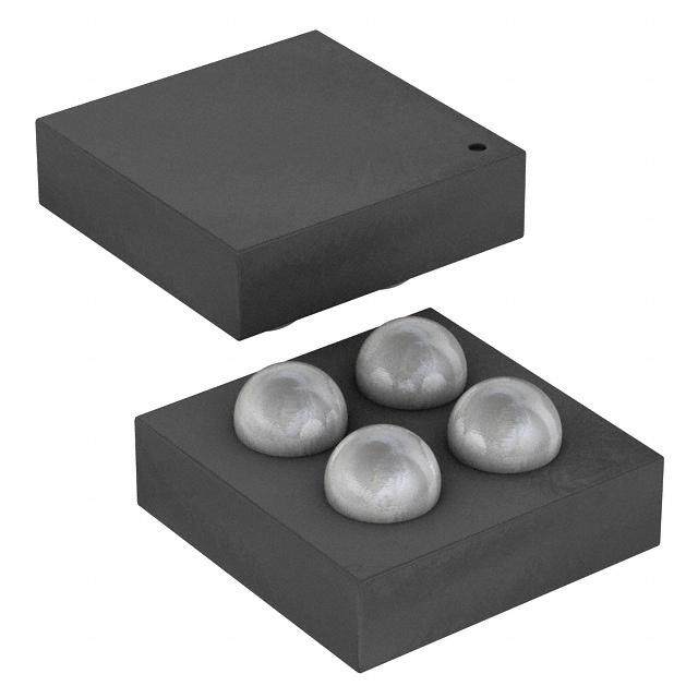
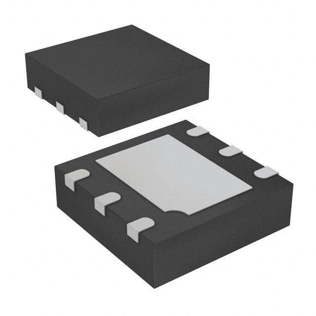
| 描述 | IC TEMP SENSOR DGTL OUT SOT23-6板上安装温度传感器 Digital Out Temperature Sensor |
| 产品分类 | |
| 品牌 | Texas Instruments |
| 产品手册 | |
| 产品图片 |
|
| rohs | 符合RoHS无铅 / 符合限制有害物质指令(RoHS)规范要求 |
| 产品系列 | 板上安装温度传感器,Texas Instruments TMP141AIDBVTSensorPath™ |
| 数据手册 | |
| 产品型号 | TMP141AIDBVT |
| 产品种类 | 板上安装温度传感器 |
| 传感器类型 | 内部 |
| 供应商器件封装 | SOT-23-6 |
| 关闭 | Shutdown |
| 其它名称 | 296-17922-6 |
| 准确性 | +/- 3 C |
| 功能 | 温度监控系统(传感器) |
| 包装 | Digi-Reel® |
| 商标 | Texas Instruments |
| 安装类型 | 表面贴装 |
| 安装风格 | SMD/SMT |
| 封装 | Reel |
| 封装/外壳 | SOT-23-6 |
| 封装/箱体 | SOT-23-6 |
| 工作温度 | -40°C ~ 125°C |
| 工厂包装数量 | 250 |
| 感应温度 | -40°C ~ 125°C |
| 拓扑 | ADC(三角积分型),寄存器库 |
| 数字输出-位数 | 10 bit |
| 数字输出-总线接口 | 1-Wire |
| 最大工作温度 | + 125 C |
| 最小工作温度 | - 40 C |
| 标准包装 | 1 |
| 电压-电源 | 2.7 V ~ 5.5 V |
| 电源电压-最大 | 5.5 V |
| 电源电压-最小 | 2.7 V |
| 电源电流 | 170 uA |
| 精度 | ±3°C(最大) |
| 系列 | TMP141 |
| 设备功能 | Sensor |
| 输出报警 | 无 |
| 输出电流 | 4 mA |
| 输出类型 | 1 线 SensorPath™ |
| 输出风扇 | 无 |
| 配置 | Local |


- 商务部:美国ITC正式对集成电路等产品启动337调查
- 曝三星4nm工艺存在良率问题 高通将骁龙8 Gen1或转产台积电
- 太阳诱电将投资9.5亿元在常州建新厂生产MLCC 预计2023年完工
- 英特尔发布欧洲新工厂建设计划 深化IDM 2.0 战略
- 台积电先进制程称霸业界 有大客户加持明年业绩稳了
- 达到5530亿美元!SIA预计今年全球半导体销售额将创下新高
- 英特尔拟将自动驾驶子公司Mobileye上市 估值或超500亿美元
- 三星加码芯片和SET,合并消费电子和移动部门,撤换高东真等 CEO
- 三星电子宣布重大人事变动 还合并消费电子和移动部门
- 海关总署:前11个月进口集成电路产品价值2.52万亿元 增长14.8%


PDF Datasheet 数据手册内容提取
Not Recommended For New Designs TMP141 SBAS347A − MARCH 2005 − REVISED JULY 2006 Digital Out Temperature Sensor with Single-Wire SensorPath Bus FEATURES DESCRIPTION (cid:1) SensorPath INTERFACE The TMP141 is a digital output temperature sensor that (cid:1) FOUR ADDRESSES utilizes the single-wire SensorPath interface. The TMP141 (cid:1) RESOLUTION: +0.25°C (10-bit) is capable of measuring temperatures within 2°C of (cid:1) WIDE TEMPERATURE RANGE: accuracy over a temperature range of −25°C to +85°C and −40°C to +125°C 3°C of accuracy over −40°C to +125°C. Low supply (cid:1) LOW QUIESCENT CURRENT: 110µA (typ) current, and a supply range from 2.7V to 5.5V, make the (cid:1) TEMPERATURE ACCURACY: ±2°C (max) TMP141 an excellent candidate for a wide range of low-power applications. The TMP141 is available in (cid:1) EXTENDED SUPPLY RANGE: +2.7V to +5.5V SOT23-6 and MSOP-8 packages. (cid:1) MICRO-SIZE PACKAGES: The TMP141 provides a simple, low-cost way to do SOT23-6 or MSOP-8 temperature measurement/monitoring and is ideal as a APPLICATIONS part of an overall hardware health monitoring system. Up to four TMP141s can be attached to a SensorPath bus. A (cid:1) MOTHERBOARDS master configures the TMP141s and reads the (cid:1) VIDEO CARDS temperature output from all devices. No external sensing (cid:1) BASE STATIONS components are needed for the TMP141 to measure and (cid:1) ROUTERS report temperature. Temperature Diode Control Temp. ADD0 Logic Sensor ∆Σ Serial V+ A/D ADD1 Interface Converter Config. GND OSC andTemp. SWD Register TMP141 Please be aware that an important notice concerning availability, standard warranty, and use in critical applications of TexasInstruments semiconductor products and disclaimers thereto appears at the end of this data sheet. SensorPath is a trademark of National Semiconductor. All other trademarks are the property of their respective owners. (cid:1)(cid:2)(cid:3)(cid:4)(cid:5)(cid:6)(cid:7)(cid:8)(cid:3)(cid:9) (cid:4)(cid:10)(cid:7)(cid:10) (cid:11)(cid:12)(cid:13)(cid:14)(cid:15)(cid:16)(cid:17)(cid:18)(cid:11)(cid:14)(cid:12) (cid:11)(cid:19) (cid:20)(cid:21)(cid:15)(cid:15)(cid:22)(cid:12)(cid:18) (cid:17)(cid:19) (cid:14)(cid:13) (cid:23)(cid:21)(cid:24)(cid:25)(cid:11)(cid:20)(cid:17)(cid:18)(cid:11)(cid:14)(cid:12) (cid:26)(cid:17)(cid:18)(cid:22)(cid:27) (cid:1)(cid:15)(cid:14)(cid:26)(cid:21)(cid:20)(cid:18)(cid:19) Copyright 2005−2006, Texas Instruments Incorporated (cid:20)(cid:14)(cid:12)(cid:13)(cid:14)(cid:15)(cid:16) (cid:18)(cid:14) (cid:19)(cid:23)(cid:22)(cid:20)(cid:11)(cid:13)(cid:11)(cid:20)(cid:17)(cid:18)(cid:11)(cid:14)(cid:12)(cid:19) (cid:23)(cid:22)(cid:15) (cid:18)(cid:28)(cid:22) (cid:18)(cid:22)(cid:15)(cid:16)(cid:19) (cid:14)(cid:13) (cid:7)(cid:22)(cid:29)(cid:17)(cid:19) (cid:8)(cid:12)(cid:19)(cid:18)(cid:15)(cid:21)(cid:16)(cid:22)(cid:12)(cid:18)(cid:19) (cid:19)(cid:18)(cid:17)(cid:12)(cid:26)(cid:17)(cid:15)(cid:26) (cid:30)(cid:17)(cid:15)(cid:15)(cid:17)(cid:12)(cid:18)(cid:31)(cid:27) (cid:1)(cid:15)(cid:14)(cid:26)(cid:21)(cid:20)(cid:18)(cid:11)(cid:14)(cid:12) (cid:23)(cid:15)(cid:14)(cid:20)(cid:22)(cid:19)(cid:19)(cid:11)(cid:12)! (cid:26)(cid:14)(cid:22)(cid:19) (cid:12)(cid:14)(cid:18) (cid:12)(cid:22)(cid:20)(cid:22)(cid:19)(cid:19)(cid:17)(cid:15)(cid:11)(cid:25)(cid:31) (cid:11)(cid:12)(cid:20)(cid:25)(cid:21)(cid:26)(cid:22) (cid:18)(cid:22)(cid:19)(cid:18)(cid:11)(cid:12)! (cid:14)(cid:13) (cid:17)(cid:25)(cid:25) (cid:23)(cid:17)(cid:15)(cid:17)(cid:16)(cid:22)(cid:18)(cid:22)(cid:15)(cid:19)(cid:27) www.ti.com
(cid:7)"(cid:1)#$# Not Recommended For New Designs www.ti.com SBAS347A − MARCH 2005 − REVISED JULY 2006 This integrated circuit can be damaged by ESD. Texas ABSOLUTE MAXIMUM RATINGS(1) Instruments recommends that all integrated circuits be Supply Voltage . . . . . . . . . . . . . . . . . . . . . . . . . . . . . . . . . . . . . . . +7V handled with appropriate precautions. Failure to observe Signal Input Terminals, Voltage(2) . . . . (V−) −0.5V to (V+) + 0.5V proper handling and installation procedures can cause damage. Signal Input Terminals, Current(2) . . . . . . . . . . . . . . . . . . . . . 10mA ESD damage can range from subtle performance degradation to Maximum Output Current (SWD low). . . . . . . . . . . . . . . . . . . 10mA complete device failure. Precision integrated circuits may be more Operating Temperature . . . . . . . . . . . . . . . . . . . . . −55°C to +127°C susceptible to damage because very small parametric changes could Storage Temperature . . . . . . . . . . . . . . . . . . . . . . . −60°C to +150°C cause the device not to meet its published specifications. Junction Temperature. . . . . . . . . . . . . . . . . . . . . . . . . . . . . . . +150°C ESD Rating: Human Body Model (HBM) . . . . . . . . . . . . . . . . . . . . . . . 4000V Charged-Device Model . . . . . . . . . . . . . . . . . . . . . . . . . . 1000V (1)Stresses above these ratings may cause permanent damage. Exposure to absolute maximum conditions for extended periods may degrade device reliability. These are stress ratings only, and functional operation of the device at these or any other conditions beyond those specified is not supported. (2)Input terminals should not be driven beyond the power-supply rails. Input signals that can swing more than 0.5V beyond the supply rails should be current-limited to 10mA or less. ORDERING INFORMATION(1) SPECIFIED PACKAGE PACKAGE ORDERING TRANSPORT PRODUCT PACKAGE-LEAD TEMPERATURE DESIGNATOR MARKING NUMBER MEDIA, QUANTITY RANGE TMP141AIDBVT Tape and Reel, 250 TTMMPP114411 SSOOTT2233--66 DDBBVV −−4400°°CC ttoo ++112255°°CC TT114411 TMP141AIDBVR Tape and Reel, 3000 TMP141AIDGKT Tape and Reel, 250 TTMMPP114411 MMSSOOPP--88 DDGGKK −−4400°°CC ttoo ++112255°°CC TT1144GG TMP141AIDGKR Tape and Reel, 3000 (1)For the most current package and ordering information, see the Package Option Addendum at the end of this document, or see the TI web site at www.ti.com. PIN CONFIGURATIONS Top View V+ 1 8 SWD ADD0 1 T 6 ADD1 T 1 GND 2 1 7 ADD1 GND 2 4 5 SWD 4 GND 3 1 4 V+ GND 3 G 6 ADD0 GND 4 5 GND SOT23−6 MSOP−8 NOTE: Pin 1 is determined by orienting the package marking as indicated in the diagram. 2
Not Recommended For New Designs (cid:7)"(cid:1)#$# www.ti.com SBAS347A − MARCH 2005 − REVISED JULY 2006 ELECTRICAL CHARACTERISTICS At TA = −40°C to +125°C and VS = +3.0V to +3.6V, unless otherwise noted. TMP141 PARAMETER CONDITIONS MIN TYP MAX UNIT TEMPERATURE INPUT Range −40 +125 °C Error TERROR T = −25°C to +85°C ±0.2 ±2 °C T = −40°C to +125°C ±3 °C vs Supply ±0.2 ±0.5 °C/V Resolution 10 Bits 0.25 °C Default Conversion Time tCONV See Table 4 for conversion time settings. 162 190 218 ms DIGITAL INPUT/OUTPUT PINS (SWD and ADD pins) Input/Output Capacitance CIN/OUT 3 pF SWD PIN Input Leakage Current IL GND < VIN < VS 0.005 10 µA IL GND < VIN < 5.5V and VS = GND/OPEN 0.005 µA Input Logic Level Voltage (High) VIH 2.1 VS + 0.5 V VS = 2.7V to 5.5V 0.6 × VS VS + 0.5 V Input Logic Level Voltage (Low) VIL −0.5 0.8 V VS = 2.7V to 5.5V −0.5 0.25 × VS V Input Hysteresis VHYST 300 mV Output Logic Level Voltage (Low) VOL IOL = 4mA 0.4 V IOL = 50µA 0.2 V Output OFF Current IOH 0.005 10 µA ADD0 and ADD1 PINS Input Leakage Current IL GND < VIN < VS 0.005 10 µA Input Logic Level Voltage (High) VIH 0.9 × VS VS + 0.5 V Input Logic Level Voltage (Low) VIL −0.5 0.1 × VS V SensorPath CHARACTERISTICS SWD Fall Time tf RPULL-UP = 1.25kΩ ± 30%, CL = 400pF 300 ns SWD Rise Time tr RPULL-UP = 1.25kΩ ± 30%, CL = 400pF 1000 ns Min. Inactive Time Between SWD Signals tINACT Bus at High Level 11 µs Master or TMP141 Reset Drive Time tRST 354 µs TMP141 Detects Bus Activity tSFEdet 9.6 µs Master Drive Time Data Bit 0 Write, Data Bit 0 Read tMtr0 11.8 17 µs Data Bit 1 Write tMtr1 35.4 48.9 µs Start Bit tMtrS 80 109 µs TMP141 Drive Time Data Bit 0−1 Read tSLout1 28.3 38.3 µs Attention Request tSLoutA 165 228 µs Reset tRST_MAX After VS is Above 2.6V 95 500 ms POWER SUPPLY Specified Voltage Range 3.0 3.6 V Operating Voltage Range 2.7 5.5 V Quiescent Current IQ Standby 80 120 µA While Converting(1) 110 170 µA Power-On Reset Voltage 1.5 2.6 V TEMPERATURE RANGE Specified Range −40 +125 °C Operating Range −55 +127 °C Storage Range −60 +150 °C Thermal Resistance (cid:1)JA MSOP-8 150 °C/W SOT23-6 200 °C/W (1)SensorPath activity only has a slight effect on quiescent current. 3
(cid:7)"(cid:1)#$# Not Recommended For New Designs www.ti.com SBAS347A − MARCH 2005 − REVISED JULY 2006 TYPICAL CHARACTERISTICS At TA = −40°C to +125°C and VS = +3.0V to +3.6V, unless otherwise noted. QUIESCENTCURRENTvsTEMPERATURE I vsTEMPERATURE STBY 200 200 180 180 5.5V 160 160 5.5V 140 140 A) µA) µ 120 ( 120 I(Q 100 3.3V ISTBY 100 2.7V 3.3V 80 80 60 60 2.7V 40 40 −55 −35 −15 5 25 45 65 85 105 125 −55 −35 −15 5 25 45 65 85 105 125 Temperature((cid:2)C) Temperature((cid:2)C) TYPICALPERFORMANCEFORTHREEUNITS TYPICALCONVERSIONTIMEvsTEMPERATURE 1.0 220 s) m 0.8 g( 210 n 0.6 etti S 200 C) 0.4 ault 3.3V 2.7V (cid:2) ef ( 0.2 D 190 or − Err 0 me 5.5V Ti 180 −0.2 on si −0.4 ver 170 n o −0.6 C 160 −55 −35 −15 5 25 45 65 85 105 125 −55 −35 −15 5 25 45 65 85 105 125 Temperature((cid:2)C) Temperature((cid:2)C) QUIESCENTCURRENTvsCONVERSIONTIME 120 PeakCurrent 110 100 A) µ 90 (Q AverageCurrent I 80 70 60 0 200 400 600 800 1000 1200 1400 1600 ConversionTime(ms) 4
Not Recommended For New Designs (cid:7)"(cid:1)#$# www.ti.com SBAS347A − MARCH 2005 − REVISED JULY 2006 0µs 50µs 100µs t DetectStart INACT t MtrS MasterWriteStart t INACT t Mtr0 MasterWrite0 t INACT SlvDetectData1 t Mtr1 MasterWrite1 1a: Master Write timing and slave detection of the data placed on the SWD bus by the master. t INACT t Mtr0 Masterstartsabit SlvDetect_st(1) Slavedetectsbusactivityand doesnothing,leavingthebita0. t SFEdet MasterRead0 1b: To place a ‘0’ on the bus, the slave does not drive the bus. t INACT t Mtr0 Masterstartsabit SlvDetect_st(1) SlavepullsBuslowtosendbacka1 t SFEdet MstDetect_1 MasterRead1 1c: To place a ‘1’ on the bus, the slave holds the bus low after detecting that the master has started a data bit. NOTE: (1) Margin from tSFEdet to tMtr0 is 2.2µs. Figure 1. TMP141 Read and Write Signal Timing 5
(cid:7)"(cid:1)#$# Not Recommended For New Designs www.ti.com SBAS347A − MARCH 2005 − REVISED JULY 2006 0µs 50µs 100µs 150µs 200µs 250µs 300µs 350µs 400µs 450µs MasterWrite0 MasterWrite1 MasterRead0 MasterRead1 t INACT t MtrS MasterWriteStart t INACT t SLoutA Sout_Attention Attention Detect t INACT Attention t RST Mout_Reset t RST Sout_Reset ResetDetect t RST Reset Figure 2. Relationship of the Five Types of Signals on SWD 6
Not Recommended For New Designs (cid:7)"(cid:1)#$# www.ti.com SBAS347A − MARCH 2005 − REVISED JULY 2006 OVERVIEW TEMPERATURE SENSING AND CONVERSION The TMP141 is a digital output temperature sensor that The TMP141 senses the absolute temperature by utilizing uses the single-wire SensorPath interface protocol. It does a diode which is part of the IC. Therefore, the sensing not require any external sensing components for device of the TMP141 is the chip itself. Thermal paths run measuring temperature. In order to minimize circuit board through the package leads as well as the plastic package, space, the TMP141 is offered in the MSOP-8 and and the lower thermal resistance of metal causes the leads SOT23-6 packages. to provide the primary thermal path. The primary usage of SensorPath-based systems is for systems that monitor hardware health. The predefined To maintain accuracy in applications that require air or SensorPath functions are: temperature measurement, surface temperature measurement, care should be taken voltage measurement, and non-volatile memory. The that the package and leads thermally connect with the specification allows for expansion by defining new surface where the temperature measurement is desired. functions or enlarging upon the predefined functions. The For example, a thermally-conductive adhesive assists in TMP141 implements the temperature measurement achieving accurate surface temperature measurements. function with a resolution of 0.25°C. Even without special precautions, because of the very low power consumption of the TMP141, self-heating will The SensorPath interface allows a master to read up to normally be well below 1LSB (0.25°C). seven slave devices on a bus, four of which can be TMP141s. The master interrogates devices on the bus to TYPICAL APPLICATION determine what they are, their capabilities, and how they can be used. Devices on the Single-Wire Data (SWD) bus The TMP141 is normally used with the address pins wired are open drain. Therefore, the SWD bus requires a 1.25kΩ high or low to select one of four possible addresses. The pull-up resistor on the bus. This resistor may be provided value read from the hardware pins plus one is stored in by the master. If the pull-up resistor is not included within register 0 as the device number. When the master the master, an external resistor must be attached to the transmits a matching device number, the TMP141 will bus. A 0.1µF capacitor is recommended for power-supply respond. In the example shown in Figure 3, ADD1:ADD0 bypassing, as shown in Figure 3. Registers inside each are wired to 2h. In this example, 3h will be stored in register device include information that identifies the device 0. When the master addresses device number 3, the capabilities, manufacturer, part ID, and even device TMP141 in Figure 3 will respond. The TMP141 will also revision number. work well in applications where ADD0:ADD1 are driven by logic levels since it reads these pins every time it does a conversion or bus transaction (see Table 2). V =3.3V S 0.1µF Optional ADD1 R=1.25kΩ SWD TMP141 Master ADD0 V SS TheresistorRmaybe integratedintothemaster. Figure 3. Typical Connections of the TMP141 7
(cid:7)"(cid:1)#$# Not Recommended For New Designs www.ti.com SBAS347A − MARCH 2005 − REVISED JULY 2006 DIGITAL INTERFACE Attention Request Up to four TMP141 devices can be connected to a single Any slave device may signal an Attention Request. Before signaling line, which is called Single-Wire Data (SWD). sending an Attention Request, the slave monitors the bus This line is similar to the data line (SMBDAT) of the to ensure that it is inactive. If an Attention Request industry-standard SMBus. The SensorPath bus uses a coincides with a data bit from another device or a Start Bit power supply of 3.3V; therefore, the signaling levels are from the master, the Attention Request will take approximately 3.3V and 0V. precedence since the Attention Request signal holds the bus low longer. The master and all communicating slaves Data is encoded in a pulse width encoding scheme. All will monitor the bus to detect an Attention Request. The signaling is done by pulling the bus low for varying lengths master monitors the bus in order to allow resending, in of time. With the exception of Reset and Attention case the Attention Request started simultaneously with a Request, the master starts all bits. Thus, when sending Start Bit or a data bit. If the master was in the midst of a data, the TMP141 does not pull the bus low. Rather, when transaction when the Attention Request was asserted, the the TMP141 needs to send a ‘1’, it first detects that the line master can either continue with the transaction by has been pulled low by the master, and then holds the line repeating the bit that was extended by the Attention low long enough to signal a ‘1’. To send a ‘0’, the TMP141 Request, initiating the next bit if a bit was not extended, or simply leaves the bus alone; the master has already it can service the Attention Request by issuing a new start placed a ‘0’ on the bus. command for a new transaction. The SWD interface used on the TMP141 has five types of Power-On Reset signals that are identified by the length of time that the line All devices on the SWD bus, including the TMP141, are is held low. Conceptually, this device operates as a required to generate a Reset signal at power up. Reset five-state signaling system. The more common signals aborts any operation in progress, and sets all registers to have shorter durations in order to speed overall the default values. The device that holds SWD low the transmission. The five signals and their approximate times longest will define how long the Reset lasts. After a Reset, are: a slave device may not send an Attention Request until the (cid:1) Data 0: Transmit a ‘0’ bit (15µs) master has sent at least 14 bits of data on the SWD bus. (cid:1) Data 1: Transmit a ‘1’ bit (42µs) Device Reset (cid:1) Start: Used by the master at the beginning of a transaction (95µs) The TMP141 will also Reset when the Reset bit is written (cid:1) to the Device Control Register (bit 0). All registers are set Attention Request: May be used by the TMP141 to to the default value. The two least significant bits of the request service (196µs) Device Control Register are the only locations that (cid:1) Reset: Must be asserted by both the master and respond to a broadcast write command from the master. slave(s) after power up. It may be asserted at other times as needed (at least 348µs). A software-programmed reset of a device by writing to its Device Control Register will not cause a Reset signal on The bus must be inactive for at least 11µs before any the bus. signal. Start BUS RESET All devices on the bus continuously monitor the bus. The master also monitors the bus to verify that it is inactive A Bus Reset occurs when the TMP141 detects a Reset before issuing a Start Bit. During the Start Bit, both the signal on the SWD bus. Upon Bus Reset, the TMP141 will master and slave(s) monitor the bus to detect an Attention abandon any communication in progress. Internal Request or a Reset. If there is an Attention Request, or a registers are not reset to their power-up values; thus, any Reset, the current signal is not treated as a Start Bit. The error flags such as BER or ORUN will remain unaffected. master may reissue the Start Bit at a later time, but is not If a conversion was in progress, it will continue to required to. completion. 8
Not Recommended For New Designs (cid:7)"(cid:1)#$# www.ti.com SBAS347A − MARCH 2005 − REVISED JULY 2006 Read and Write Transactions A complete Read transmission consists of a Start Bit, the device number, the Register Number, R/W = 1, the data bits, an even parity bit, and an Acknowledge bit. The most significant bit is sent first. Read Transaction START DEVICE NUMBER REGISTER NUMBER R/W 8 or 16 DATA BITS EP ACK M M M M M M M M M M M S … S S M A complete Write transmission consists of a Start Bit, the device number, the Register Number, R/W = 0, the data bits, an even parity bit, and an Acknowledge bit. Write Transaction START DEVICE NUMBER REGISTER NUMBER R/W 8 or 16 DATA BITS EP ACK M M M M M M M M M M M M … M M S M indicates that the bit is initiated and controlled by the master. S indicates that the bit is initiated by the master but controlled by the slave; if the data is a ‘1’, the slave lengthens the time that the bus is held low to signal a ‘1’. The device number is three bits long. Device number 0 is reserved for a broadcast to all devices, leaving address space for seven slaves. The Register Number is six bits long. The R/W is a ‘1’ for a read operation. The R/W bit is a ‘0’ for a write operation. All data bits are started by the master pulling the bus low. The TMP141 will detect the bus being low within time t . SFEdet If it is a read transaction and the TMP141 needs to send a ‘1’ for that bit period, it will hold the bus low for time t . SLout1 In a Write operation, the data bits and parity are sent by the master. In a Read operation, the data bits and parity are sent by the TMP141. Data length is eight bits for registers 0, 4, and 20h. All other registers are 16 bits long. The number of bits transmitted or received depends on the length of the register: 8 bits for an 8-bit register and 16 bits for a 16-bit register. Even parity (EP) is used on the SensorPath. The parity calculation includes all bits after the Start Bit, up to and including the parity bit. Thus, the parity calculation includes the device number, the Register Number, R/W, the data bits, and the parity bit. In a Write operation, the TMP141 checks the parity sent by the master before generating the Acknowledge bit. The Acknowledge bit is sent by the receiving unit. In a Write operation, the Acknowledge bit will come from the TMP141. In a Read operation, the master generates the Acknowledge bit. ACKNOWLEDGE Bit Definition: 1: A complete data transmission was completed without a parity error. 0: An error was detected. (BER in the Status Register will be set. An Attention Request will be generated.) 9
(cid:7)"(cid:1)#$# Not Recommended For New Designs www.ti.com SBAS347A − MARCH 2005 − REVISED JULY 2006 APPLICATIONS INFORMATION Table 1. Register Set Summary RESET BIT POSITION (MSB to the left. In a transmission, the MSB is sent first.) AADDDDRREESSSS VVAALLUUEE (hex) NAME R/W (hex) 15 14 13 12 11 10 9 8 7 6 5 4 3 2 1 0 DDeevviiccee Reserved See Table 2 00 RR 11((11)) NNoott AAvvaaiillaabbllee ((tthhiiss rreeggiisstteerr iiss 88 bbiittss lloonngg)) NNuummbbeerr 0 0 0 0 0 AS2 AS1 AS0 Manufacturer 1 R 104C 0 0 0 1 0 0 0 0 0 1 0 0 1 1 0 0 ID Revision ID Device ID 22 DDeevviiccee IIDD RR 88DD 0 0 0 0 0 0 0 0 1 0 0 0 1 1 0 1 Reserved Function 1 33 CCaappaabbiilliittiieess RR 11 0 0 0 0 0 0 0 0 0 0 0 0 0 0 0 1 4 Status R 0 Not Available (this register is 8 bits long) BER 0 0 ORUN 0 0 0 SF1 DDeevviiccee Reserved Res LLooww SShhuutt 55 RR//WW 00 EENNAABB RReesseett CCoonnttrrooll 0 0 0 0 0 0 0 0 0 0 0 0 PPwwrr DDoowwnn Reserved Internal ROUT Sign Result is10 Bits Resolution Is 0.25°C Temperature Sense Size 88 RR 001144AA CCaappaabbiilliittiieess 0 0 0 0 0 0 0 1 0 1 0 0 1 0 1 0 TTeemmppeerraattuurree Reserved 99 RR 00 SSiiggnn 6644°°CC 3322°°CC 1166°°CC 88°°CC 44°°CC 22°°CC 11°°CC 00..55°°CC 00..2255°°CC RReeaaddoouutt 0 0 0 0 0 0 TTeemmppeerraattuurree AA RR//WW 00 EENN__SS AATT__EE CCoonnttrrooll 0 0 0 0 0 0 0 0 0 0 0 0 0 0 B−1F Reserved R Undefined Conversion Conversion 20 R/W 2(2) Not Available (this register is 8 bits long) 0 0 0 0 0 0 Rate Rate 21−3F Undefined Undefined (1)See Table 2 for the value of register 0 at Reset. (2)See Table 4 for the conversion rate settings. REGISTER DETAILS Device number 000b is the broadcast address reserved for communicating with all devices, and can be responded to Register 0: Device Number (Read-Only) by all slave devices. The TMP141 ignores a broadcast Register 0 is an 8-bit register. The device number is Read transaction. A broadcast Write message may be created from the inputs at the address pins. The result is used to write to the Device Control Register, which is the placed in Register 0 according to Table 2. only register which responds to broadcast messages (see the Device Control Register description). Table 2. Device Number—Assignments Register 1: Manufacturer ID (Read-Only) ADD1:ADD0 AS2:AS0 The Manufacturer ID for Texas Instruments is 104Ch. BITS 2:0 00 001 Register 2: Device ID (Read-Only) 01 010 The device ID is unique for each device produced by TI. Bits 10:0 contain 8Dh, which is the identifier for the 10 011 TMP141. Bits 15:11 identify the revision of the die and will 11 100 be incremented upon device revision. Register 3: Capabilities (Read-Only) ADD1 and ADD0 are the physical pins used to define the address to which the TMP141 responds to—they are not Function 1 for the TMP141 is temperature measurement; the actual addresses. AS2:AS0 is the address to which the this is the only function defined for the TMP141. This device responds. register has the value of 1h. 10
Not Recommended For New Designs (cid:7)"(cid:1)#$# www.ti.com SBAS347A − MARCH 2005 − REVISED JULY 2006 Register 4: Device Status (Read-Only) Register 8: Temperature Capabilities (Read-Only) This is an 8-bit register with the following bits defined: Bits 15−9: Reserved. These bits read as ‘0’. Bit 7, Bus Error (BER): This bit is set whenever there is Bit 8: This bit is set, indicating that the internal temperature an error indication in the Acknowledge bit of either sensing is the only option available. received or transmitted data. A bus error is cleared when the master reads the Device Status Register or sends Bit 7: This bit is ‘0’; it indicates that the TMP141 Tempera- Device Reset. ture Readout register is 16 bits. Bits 6−5: Reserved. These bits read as ‘0’. Bit 6: This bit is set to indicate that signed two’s Bit 4, Overrun (ORUN): This flag is set when another complement is the format of the temperature data. temperature conversion is completed before the previous Bits 5−3: These bits are 001b; they indicate that the conversion has been read by the master. This error is temperature data is 10 bits long. cleared by Device Reset, or by reading the temperature result from the Temperature Readout register. Bits 2−0: These bits are 010b, and indicate that the Bits 3−1: Reserved. These bits read as ‘0’. temperature data resolution is 0.25°C. Bit 0, Status Function 1 (SF1): This flag is set when a Register 9: Temperature Readout (Read-Only) temperature conversion is completed, and the data is stored in the Readout register. It is reset either when the The TMP141 outputs 10 bits of precision to a resolution of master reads the temperature conversion, or when the 0.25°C. This 10-bit format covers a range from +127.75°C TMP141 is reset. to −128°C. Negative numbers are in two’s complement. Register 5: Device Control (Read/Write) Table 3 shows some examples of the Temperature Data Bits 15−5: Reserved. These bits read as ‘0’. format. Bit 4, Enable Function 1 (ENAB): This bit enables Data is left-justified, meaning that the ten bits of data are temperature measurement; the default setting is disabled. in the most significant bits of this register. The temperature To begin temperature measurement, a ‘1’ must be written data is contained in Bits 15:6. Bits 5:0 always read as ‘0’. to this bit. The enable sensor bit (EN_S) in the Temperature Control register must also be set to enable Table 3. Data Format Example the sensor. (Bits cannot be written individually; a Write operation affects the entire register.) TEMPERATURE BINARY HEX Bit 3: Reserved. This bit reads as ‘0’. +127.75°C(1) 01 1111 1111 1FFh Bit 2, Low-Power Mode: When this bit is set, the +125.00°C 01 1111 0100 1F4h operation of all functions slow down in order to conserve +100.0°C 01 1001 0000 190h power. Default is ‘0’ for normal speed operation. (See +1.0°C 00 0000 0100 004h Table 4.) +0.25°C 00 0000 0001 001h Bit 1, Shutdown: When this bit is set, all functions are 0°C 00 0000 0000 000h disabled, placing the TMP141 in the lowest possible power consumption mode. Default is ‘0’; this is normal operation. −0.25°C 11 1111 1111 3FFh To exit shutdown, write a ‘0’ to this location. −1.0°C 11 1111 1100 3FCh Bit 0, Reset: When this bit is set, the TMP141 performs a −100°C 10 0111 0000 270h Device Reset. During Reset, any operation is progress is −128°C(1) 10 0000 0000 200h aborted, and all registers are set to their default values. This bit self-clears when the Reset operation is completed. (1)Both −128°C and +127.75°C are beyond the specified operating range of −40°C to +125°C. This table only illustrates the format It is not necessary to do a Device Reset after power-up. of the data. Bits 1−0: These bits are the only location in the TMP141 that accepts a broadcast Write message. 11
(cid:7)"(cid:1)#$# Not Recommended For New Designs www.ti.com SBAS347A − MARCH 2005 − REVISED JULY 2006 Register Ah: Temperature Control (Read/Write) Register 20h: Conversion Rate (Read/Write) Bits 15−2: Reserved. These bits read as ‘0’. The conversion rate is controlled by both the low-power bit Bit 1, Enable Sensor (EN_S): Default is ‘0’, which is the in the Device Control register, and the Conversion Rate disabled state. In addition to setting this bit, the enable bit setting in the Conversion Rate register. This register is in register 5 must also be set in order to measure device-specific, and therefore not defined by the temperature. SensorPath specification. The conversion rate for a given application is chosen based on system requirements and Bit 0, Attention Enable (AT_E): Default is disabled. limitations, such as the thermal response time of the When this bit is set, and the sensor is enabled (bit 1), the system (including the TMP141). TMP141 will generate Attention Requests. If enabled, an Attention Request will be generated when a bit is set in the Device Status register (register 4). See Figure 5 for the Table 4. Conversion Time Settings details on the conditions for generating an Attention Request. CONVERSION TYPICAL Note: A bus error always attempts to generate an Attention LOW-POWER RATE SETTING CONVERSION MODE (register 20h, bits TIME Request. (register 5, bit 2) 1−0 binary) (ms) (For more information on the Attention Request 0 00 64 conditions, see the flowcharts in Figure 4 and Figure 5, and the information on Exception Handling on page 14.) 1 00 96 0 01 96 The rules for generating an Attention Request are different, depending on whether it was caused by a bus 1 01 382 error or a temperature conversion. A bus error always 0 10 190 (default) attempts to generate an Attention Request, whereas a 1 10 766 conversion or a conversion overrun has several conditions 0 11 382 that may prevent the assertion of Attention Request. These differences are illustrated in Figure 4 and Figure 5. 1 11 1532 12
Not Recommended For New Designs (cid:7)"(cid:1)#$# www.ti.com SBAS347A − MARCH 2005 − REVISED JULY 2006 Attention Request Flowfor Conversion Complete AttentionRequest FlowforBusError Conversion No Ready? No Yes BusError? Yes No SF=1? SetSF=1 SetBER=1 Yes SetORUN=1 Yes BusReset? Attention No Request No Enabled (AT_E)? Yes Yes DeviceReset? SetBER=0 Attention No Yes Request Service Pending? No No BusFree? Yes No BusFree? Generate Attention Request Yes Generate Attention Request Figure 4. Attention Request Generated by a Bus Figure 5. Attention Request Generated by a Error Conversion Complete 13
(cid:7)"(cid:1)#$# Not Recommended For New Designs www.ti.com SBAS347A − MARCH 2005 − REVISED JULY 2006 EXCEPTION HANDLING an ACK bit of ‘1’ is not received during a Write transaction, the TMP141 will not perform any internal operations based ATTENTION REQUEST on that transaction. A transaction with an Acknowledge bit Two conditions can cause the TM141 to generate an of 0 is not considered complete by the TMP141, and the Attention Request: a conversion completion and a bus following actions are performed: error. 1. The bus error bit in the TMP141 Device Status register Upon completion of a conversion, an Attention Request is set. may be asserted if an Attention Request is enabled (bit 0 in the Temperature Control register), if the bus is inactive, 2. The TMP141 generates an Attention Request before and if there has not been an Attention Request on the bus (or together with) the Start Bit of the next transaction. since the Device Status register was last read or the last A transaction that was not positively acknowledged is also bus reset. not considered complete by the master (that is, the master will not use data that it received from a transaction that was A slave generates an Attention Request by holding the bus not acknowledged). The transaction may be repeated by low for time t . Because it is longer than any other SLoutA the master after detecting the source of the Attention signal (except Reset), it takes priority over the other bus Request (the TMP141 or other slave that has a set BER bit signals (Start, Data 1, and Data 0). in the Device Status Register). Note that the SensorPath protocol neither forces, nor automates re-execution of, the ATTENTION REQUEST SERVICE transaction by the master. The master is required to read the status register of all Incomplete Transactions: slaves after an Attention Request to determine which If the TMP141 receives a Start Bit during a transaction, it slave sent the request. While an Attention Request service aborts the current transaction, and begins a new one. This is pending, no slave can generate another Attention process is not recommended, but is a legal operation. No Request to request a read of its Temperature Readout error will be generated. register. However, Attention Requests caused by bus If excess bits are received, the extra bits are ignored. The errors will continue to be generated. TMP141 expects the parity (EP) and acknowledge (ACK) bits in the usual places. However, in such cases, there is ACKNOWLEDGE (ACK) usually a parity error, and the transaction is not acknowledged. Error handling proceeds as described in During a Read transaction, the master sends the ACK bit the Acknowledge section. to indicate that the even parity (EP) bit was received, found to be correct when compared to the data preceding it, and If insufficient bits are received, the TMP141 will wait no conflict was detected on the bus. During a Write indefinitely for the missing bits. If the master starts a new transaction, the slave sends the ACK bit with the same transaction before those bits are received, the TMP141 meaning as when the master sends it. A transaction is abandons the current transaction, and begins the new considered complete only when the ACK bit is received. If transaction. No error is generated. 14
Not Recommended For New Designs (cid:7)"(cid:1)#$# www.ti.com SBAS347A − MARCH 2005 − REVISED JULY 2006 GLOSSARY ACK (Acknowledge Bit): The bit that concludes a transmission indicating whether any errors were detected in the transmission. A ‘1’ indicates that no errors were found; a ‘0’ indicates an error. An acknowledge error causes BER to be set. BER will be set regardless of whether the device or the master generates the acknowledge error. AT_E (Attention Enable): This is the LSB in the Temperature Control register (bit 0, register Ah). When set, the TMP141 will generate Attention Requests. If enabled, an Attention Request will be generated when a conversion is complete. BER (Bus Error): A flag that is set when the TMP141 either generates or receives an Acknowledge error (bit 7 in the Status register). EN_S: (Sensor Enable Bit): This is bit 1 in the Temperature Control register. When set, temperature measurement is enabled. Default setting is disabled. To report temperature, ENAB must also be set. ENAB (Enable Temperature Sensing): This is a bit in the Device Control register. In the case of the TMP141, function 1 is temperature measurement. Setting this bit will enable temperature measurement (bit 4 in the Device Control register). The sensor should also be turned on by the Sensor Enable flag (bit 1) in the Temperature Control register. Even Parity: The number of bits in a transmission that are ‘1’ is even. The SensorPath uses even parity. All bits after the start bit (up to and including the parity bit) are included in this calculation, but the ACK bit is not. ORUN (Overrun Error): This flag is set when a temperature conversion is completed before the previous conversion has been read by the master (bit 4 in the Device Status register). If other conditions are met, overrun will generate an Attention Request. PCI SIG (assigned identifiers): The ID for Texas Instruments is 104Ch. This number is programmed into the Manufacturer ID register. Other IDs can be fond at http://www.pcisig.com/membership/vid_search/. This number enables identification of the device manufacturer (which can be useful in determining the features of a device) and to perform manufacturer-specific operations. There are no vendor-specific operations for the TMP141—all of the operations conform to industry standards. Pulse Width Encoding: A signaling scheme whereby the information is differentiated by the width of the pulse. In the case of SensorPath, the pulses are created by pulling the bus low. The length of time that it is low determines the meaning of that pulse. See the Digital Interface section on page 8. SF1 (Status Function One): This flag is set when a temperature conversion is completed, and the data is stored in the Readout register. It is reset when the master reads the temperature conversion, or when the TMP141 is reset. Shutdown Mode: A very low-power state entered when the master writes to the shutdown bit (bit 1) in the Device Control register. In the shutdown state, temperature conversions are stopped. The TMP141 consumes the lowest possible power in this state (see also Low-Power Mode on page 11). SWCLK: Single-Wire Clock, an optional signal used only when the SensorPath is used in synchronous mode. The TMP141 does not use and does not support this option. Systems that use SWCLK are using a two-wire SensorPath bus. SWD (Single-Wire Data): The line used to communicate between master and slave devices as required by the specified SensorPath. Five types of signals go over this line (Zero, One, Start, Attention Request, and Reset). Signals are differentiated by the length of time that they hold the bus low. This is the only line used to communicate between the slaves, such as the TMP141, and the master. A 1.25kΩ pull-up resistor may be integrated into the master, or it may be external. Synchronous Mode: An optional mode used with SensorPath devices that do not meet the ±15% clock timing accuracy requirement. The TMP141 clock meets the clock accuracy requirement, and therefore does not support the synchronous mode (see SWCLK). 15
PACKAGE OPTION ADDENDUM www.ti.com 24-Aug-2018 PACKAGING INFORMATION Orderable Device Status Package Type Package Pins Package Eco Plan Lead/Ball Finish MSL Peak Temp Op Temp (°C) Device Marking Samples (1) Drawing Qty (2) (6) (3) (4/5) TMP141AIDBVT NRND SOT-23 DBV 6 250 Green (RoHS CU NIPDAU Level-2-260C-1 YEAR -40 to 125 T141 & no Sb/Br) TMP141AIDGKR NRND VSSOP DGK 8 2500 Green (RoHS CU NIPDAU | Level-2-260C-1 YEAR -40 to 125 T14G & no Sb/Br) CU NIPDAUAG TMP141AIDGKT NRND VSSOP DGK 8 250 Pb-Free CU NIPDAUAG Level-2-260C-1 YEAR -40 to 125 T14G (RoHS) (1) The marketing status values are defined as follows: ACTIVE: Product device recommended for new designs. LIFEBUY: TI has announced that the device will be discontinued, and a lifetime-buy period is in effect. NRND: Not recommended for new designs. Device is in production to support existing customers, but TI does not recommend using this part in a new design. PREVIEW: Device has been announced but is not in production. Samples may or may not be available. OBSOLETE: TI has discontinued the production of the device. (2) RoHS: TI defines "RoHS" to mean semiconductor products that are compliant with the current EU RoHS requirements for all 10 RoHS substances, including the requirement that RoHS substance do not exceed 0.1% by weight in homogeneous materials. Where designed to be soldered at high temperatures, "RoHS" products are suitable for use in specified lead-free processes. TI may reference these types of products as "Pb-Free". RoHS Exempt: TI defines "RoHS Exempt" to mean products that contain lead but are compliant with EU RoHS pursuant to a specific EU RoHS exemption. Green: TI defines "Green" to mean the content of Chlorine (Cl) and Bromine (Br) based flame retardants meet JS709B low halogen requirements of <=1000ppm threshold. Antimony trioxide based flame retardants must also meet the <=1000ppm threshold requirement. (3) MSL, Peak Temp. - The Moisture Sensitivity Level rating according to the JEDEC industry standard classifications, and peak solder temperature. (4) There may be additional marking, which relates to the logo, the lot trace code information, or the environmental category on the device. (5) Multiple Device Markings will be inside parentheses. Only one Device Marking contained in parentheses and separated by a "~" will appear on a device. If a line is indented then it is a continuation of the previous line and the two combined represent the entire Device Marking for that device. (6) Lead/Ball Finish - Orderable Devices may have multiple material finish options. Finish options are separated by a vertical ruled line. Lead/Ball Finish values may wrap to two lines if the finish value exceeds the maximum column width. Important Information and Disclaimer:The information provided on this page represents TI's knowledge and belief as of the date that it is provided. TI bases its knowledge and belief on information provided by third parties, and makes no representation or warranty as to the accuracy of such information. Efforts are underway to better integrate information from third parties. TI has taken and continues to take reasonable steps to provide representative and accurate information but may not have conducted destructive testing or chemical analysis on incoming materials and chemicals. TI and TI suppliers consider certain information to be proprietary, and thus CAS numbers and other limited information may not be available for release. Addendum-Page 1
PACKAGE OPTION ADDENDUM www.ti.com 24-Aug-2018 In no event shall TI's liability arising out of such information exceed the total purchase price of the TI part(s) at issue in this document sold by TI to Customer on an annual basis. Addendum-Page 2
PACKAGE MATERIALS INFORMATION www.ti.com 1-May-2019 TAPE AND REEL INFORMATION *Alldimensionsarenominal Device Package Package Pins SPQ Reel Reel A0 B0 K0 P1 W Pin1 Type Drawing Diameter Width (mm) (mm) (mm) (mm) (mm) Quadrant (mm) W1(mm) TMP141AIDGKR VSSOP DGK 8 2500 330.0 12.4 5.3 3.4 1.4 8.0 12.0 Q1 TMP141AIDGKT VSSOP DGK 8 250 180.0 12.4 5.3 3.4 1.4 8.0 12.0 Q1 PackMaterials-Page1
PACKAGE MATERIALS INFORMATION www.ti.com 1-May-2019 *Alldimensionsarenominal Device PackageType PackageDrawing Pins SPQ Length(mm) Width(mm) Height(mm) TMP141AIDGKR VSSOP DGK 8 2500 367.0 367.0 35.0 TMP141AIDGKT VSSOP DGK 8 250 210.0 185.0 35.0 PackMaterials-Page2
PACKAGE OUTLINE DBV0006A SOT-23 - 1.45 mm max height SCALE 4.000 SMALL OUTLINE TRANSISTOR C 3.0 2.6 0.1 C 1.75 1.45 B A 1.45 MAX PIN 1 INDEX AREA 1 6 2X 0.95 3.05 2.75 1.9 5 2 4 3 0.50 6X 0.25 0.15 0.2 C A B (1.1) TYP 0.00 0.25 GAGE PLANE 0.22 TYP 0.08 8 TYP 0.6 0 0.3 TYP SEATING PLANE 4214840/B 03/2018 NOTES: 1. All linear dimensions are in millimeters. Any dimensions in parenthesis are for reference only. Dimensioning and tolerancing per ASME Y14.5M. 2. This drawing is subject to change without notice. 3. Body dimensions do not include mold flash or protrusion. Mold flash and protrusion shall not exceed 0.15 per side. 4. Leads 1,2,3 may be wider than leads 4,5,6 for package orientation. 5. Refernce JEDEC MO-178. www.ti.com
EXAMPLE BOARD LAYOUT DBV0006A SOT-23 - 1.45 mm max height SMALL OUTLINE TRANSISTOR PKG 6X (1.1) 1 6X (0.6) 6 SYMM 2 5 2X (0.95) 3 4 (R0.05) TYP (2.6) LAND PATTERN EXAMPLE EXPOSED METAL SHOWN SCALE:15X SOLDER MASK SOLDER MASK METAL UNDER METAL OPENING OPENING SOLDER MASK EXPOSED METAL EXPOSED METAL 0.07 MAX 0.07 MIN ARROUND ARROUND NON SOLDER MASK SOLDER MASK DEFINED DEFINED (PREFERRED) SOLDER MASK DETAILS 4214840/B 03/2018 NOTES: (continued) 6. Publication IPC-7351 may have alternate designs. 7. Solder mask tolerances between and around signal pads can vary based on board fabrication site. www.ti.com
EXAMPLE STENCIL DESIGN DBV0006A SOT-23 - 1.45 mm max height SMALL OUTLINE TRANSISTOR PKG 6X (1.1) 1 6X (0.6) 6 SYMM 2 5 2X(0.95) 3 4 (R0.05) TYP (2.6) SOLDER PASTE EXAMPLE BASED ON 0.125 mm THICK STENCIL SCALE:15X 4214840/B 03/2018 NOTES: (continued) 8. Laser cutting apertures with trapezoidal walls and rounded corners may offer better paste release. IPC-7525 may have alternate design recommendations. 9. Board assembly site may have different recommendations for stencil design. www.ti.com
None
None
IMPORTANTNOTICEANDDISCLAIMER TIPROVIDESTECHNICALANDRELIABILITYDATA(INCLUDINGDATASHEETS),DESIGNRESOURCES(INCLUDINGREFERENCE DESIGNS),APPLICATIONOROTHERDESIGNADVICE,WEBTOOLS,SAFETYINFORMATION,ANDOTHERRESOURCES“ASIS” ANDWITHALLFAULTS,ANDDISCLAIMSALLWARRANTIES,EXPRESSANDIMPLIED,INCLUDINGWITHOUTLIMITATIONANY IMPLIEDWARRANTIESOFMERCHANTABILITY,FITNESSFORAPARTICULARPURPOSEORNON-INFRINGEMENTOFTHIRD PARTYINTELLECTUALPROPERTYRIGHTS. TheseresourcesareintendedforskilleddevelopersdesigningwithTIproducts.Youaresolelyresponsiblefor(1)selectingtheappropriate TIproductsforyourapplication,(2)designing,validatingandtestingyourapplication,and(3)ensuringyourapplicationmeetsapplicable standards,andanyothersafety,security,orotherrequirements.Theseresourcesaresubjecttochangewithoutnotice.TIgrantsyou permissiontousetheseresourcesonlyfordevelopmentofanapplicationthatusestheTIproductsdescribedintheresource.Other reproductionanddisplayoftheseresourcesisprohibited.NolicenseisgrantedtoanyotherTIintellectualpropertyrightortoanythird partyintellectualpropertyright.TIdisclaimsresponsibilityfor,andyouwillfullyindemnifyTIanditsrepresentativesagainst,anyclaims, damages,costs,losses,andliabilitiesarisingoutofyouruseoftheseresources. TI’sproductsareprovidedsubjecttoTI’sTermsofSale(www.ti.com/legal/termsofsale.html)orotherapplicabletermsavailableeitheron ti.comorprovidedinconjunctionwithsuchTIproducts.TI’sprovisionoftheseresourcesdoesnotexpandorotherwisealterTI’sapplicable warrantiesorwarrantydisclaimersforTIproducts. MailingAddress:TexasInstruments,PostOfficeBox655303,Dallas,Texas75265 Copyright©2019,TexasInstrumentsIncorporated