ICGOO在线商城 > 传感器,变送器 > 温度传感器 - 模拟和数字输出 > AD7814ARTZ-REEL7
 Datasheet下载
- 型号: AD7814ARTZ-REEL7
- 制造商: Analog
- 库位|库存: xxxx|xxxx
- 要求:
| 数量阶梯 | 香港交货 | 国内含税 |
| +xxxx | $xxxx | ¥xxxx |
查看当月历史价格
查看今年历史价格
AD7814ARTZ-REEL7产品简介:
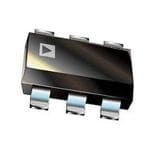
ICGOO电子元器件商城为您提供AD7814ARTZ-REEL7由Analog设计生产,在icgoo商城现货销售,并且可以通过原厂、代理商等渠道进行代购。 AD7814ARTZ-REEL7价格参考。AnalogAD7814ARTZ-REEL7封装/规格:温度传感器 - 模拟和数字输出, Temperature Sensor Digital, Local -55°C ~ 125°C 10 b SOT-23-6。您可以下载AD7814ARTZ-REEL7参考资料、Datasheet数据手册功能说明书,资料中有AD7814ARTZ-REEL7 详细功能的应用电路图电压和使用方法及教程。
AD7814ARTZ-REEL7是Analog Devices Inc.生产的一款具有模拟和数字输出的温度传感器,属于低功耗、高精度的集成电路温度传感器。该器件主要适用于对空间和功耗敏感的便携式设备与工业控制系统。

其典型应用场景包括:便携式医疗设备(如电子体温计、可穿戴健康监测设备),用于实时监测人体或环境温度;通信设备中的热管理,例如基站模块、网络路由器等,用以监控系统内部温度并防止过热;工业自动化控制系统中对电机、电源模块等关键部件的温度监控;此外,还可用于计算机系统(如笔记本电脑、嵌入式主板)中的CPU或电池温度检测,实现动态散热管理。

AD7814ARTZ-REEL7采用SOT-23-6小型封装,适合高密度PCB布局,并支持I²C兼容的数字接口输出,同时具备模拟电压输出功能,便于与多种类型的微控制器连接。其工作温度范围宽(通常为-55°C至+125°C),适应严苛环境下的稳定运行。由于具备关断模式,显著降低待机功耗,特别适用于电池供电设备。

综上,AD7814ARTZ-REEL7广泛应用于需要精确、可靠且低功耗温度监测的消费电子、工业控制、通信和医疗等领域。
| 参数 | 数值 |
| 产品目录 | 集成电路 (IC)热管理产品 |
| 描述 | IC TEMP SNSR 10BIT DGTL SOT23-6板上安装温度传感器 10-BIT DIGITAL IC |
| 产品分类 | |
| 品牌 | Analog Devices Inc |
| 产品手册 | |
| 产品图片 |
|
| rohs | 符合RoHS无铅 / 符合限制有害物质指令(RoHS)规范要求 |
| 产品系列 | 板上安装温度传感器,Analog Devices AD7814ARTZ-REEL7- |
| 数据手册 | |
| 产品型号 | AD7814ARTZ-REEL7 |
| 产品目录页面 | |
| 产品种类 | 板上安装温度传感器 |
| 传感器类型 | 内部 |
| 供应商器件封装 | SOT-23-6 |
| 其它名称 | AD7814ARTZ-REEL7-ND |
| 准确性 | 2 C |
| 功能 | 温度监控系统(传感器) |
| 包装 | 带卷 (TR) |
| 商标 | Analog Devices |
| 安装类型 | 表面贴装 |
| 安装风格 | SMD/SMT |
| 封装 | Reel |
| 封装/外壳 | SOT-23-6 |
| 封装/箱体 | SOT-23-6 |
| 工作温度 | -55°C ~ 125°C |
| 工厂包装数量 | 3000 |
| 感应温度 | -55°C ~ 125°C |
| 拓扑 | ADC,寄存器库 |
| 数字输出-位数 | 10 bit |
| 数字输出-总线接口 | 3-Wire, Microwire, SPI |
| 最大工作温度 | + 125 C |
| 最小工作温度 | - 55 C |
| 标准包装 | 3,000 |
| 电压-电源 | 2.7 V ~ 5.5 V |
| 电源电压-最大 | 5.5 V |
| 电源电压-最小 | 2.7 V |
| 电源电流 | 400 uA |
| 精度 | ±2°C |
| 系列 | AD7814 |
| 视频文件 | http://www.digikey.cn/classic/video.aspx?PlayerID=1364138032001&width=640&height=505&videoID=2245193158001 |
| 设备功能 | Temperature Sensor |
| 输出报警 | 无 |
| 输出类型 | MICROWIRE, QSPI, SPI |
| 输出风扇 | 无 |
| 配置 | Local |


- 商务部:美国ITC正式对集成电路等产品启动337调查
- 曝三星4nm工艺存在良率问题 高通将骁龙8 Gen1或转产台积电
- 太阳诱电将投资9.5亿元在常州建新厂生产MLCC 预计2023年完工
- 英特尔发布欧洲新工厂建设计划 深化IDM 2.0 战略
- 台积电先进制程称霸业界 有大客户加持明年业绩稳了
- 达到5530亿美元!SIA预计今年全球半导体销售额将创下新高
- 英特尔拟将自动驾驶子公司Mobileye上市 估值或超500亿美元
- 三星加码芯片和SET,合并消费电子和移动部门,撤换高东真等 CEO
- 三星电子宣布重大人事变动 还合并消费电子和移动部门
- 海关总署:前11个月进口集成电路产品价值2.52万亿元 增长14.8%


PDF Datasheet 数据手册内容提取
a 10-Bit Digital Temperature Sensor in 6-Lead SOT-23 AD7814 FEATURES FUNCTIONAL BLOCK DIAGRAM 10-Bit Temperature-to-Digital Converter –55(cid:1)C to +125(cid:1)C Operating Temperature Range (cid:2)2(cid:1)C Accuracy BAND GAP 10-BIT TEMPERATURE ANALOG/DIGITAL SPI- and DSP-Compatible Serial Interface SENSOR CONVERTER Shutdown Mode Space-Saving SOT-23 Package GND VDD TEMPERATURE AD7814 VALUE APPLICATIONS REGISTER Hard Disk Drives Personal Computers CS Electronic Test Equipment SERIAL SCLK BUS Office Equipment INTERFACE DIN Domestic Appliances DOUT Process Control GENERAL DESCRIPTION PRODUCT HIGHLIGHTS The AD7814 is a complete temperature monitoring system in a 1. The AD7814 has an on-chip temperature sensor that allows SOT-23 package or 8-lead MSOP package. It contains a band an accurate measurement of the ambient temperature. The gap temperature sensor and 10-bit ADC to monitor and digitize measurable temperature range is –55°C to +125°C, with a the temperature reading to a resolution of 0.25°C. ±2°C temperature accuracy. The AD7814 has a flexible serial interface that allows easy inter- 2. Supply voltage of 2.7 V to 5.5 V facing to most microcontrollers. The interface is compatible 3. Space-saving 6-lead SOT-23 package and 8-lead MSOP with SPI®, QSPI™, and MICROWIRE™ protocol, and is also package compatible with DSPs. The part features a standby mode that is 4. 10-bit temperature reading to 0.25°C resolution controlled via the serial interface. 5. Standby mode that reduces the current consumption to 1µA The AD7814’s wide supply voltage range, low supply current, and SPI-compatible interface make it ideal for a variety of applications, including personal computers, office equipment, and domestic appliances. Purchase of licensed I2C components of Analog Devices or one of its sublicensed Associated Companies conveys a license for the purchaser under the Philips I2C Patent Rights to use these components in an I2C system, provided that the system conforms to the I2C Standard Specification as defined by Philips. REV. E Information furnished by Analog Devices is believed to be accurate and reliable. However, no responsibility is assumed by Analog Devices for its use, nor for any infringements of patents or other rights of third parties that may result from its use. No license is granted by implication or otherwise One Technology Way, P.O. Box 9106, Norwood, MA 02062-9106, U.S.A. under any patent or patent rights of Analog Devices. Trademarks and Tel: 781/329-4700 www.analog.com registered trademarks are the property of their respective owners. Fax: 781/326-8703 © 2004 Analog Devices, Inc. All rights reserved.
AD7814–SPECIFICATIONS1 (T = T to T , V = 2.7 V to 5.5 V, unless otherwise noted.) A MIN MAX DD Parameter Min Typ Max Unit Test Conditions/Comments TEMPERATURE SENSOR AND ADC Accuracy ±2.0 °C T = 0°C to 85°C. V = 3 V to 5.5 V2 A DD ±2.5 °C T = –40°C to 0°C. V = 3 V to 5.5 V2 A DD ±2.0 ±3.5 °C T = –55°C to +125°C. V = 3 V to 5.5 V A DD Resolution 10 Bits Update Rate, t 400 µs R Temperature Conversion Time 25 µs SUPPLIES Supply Voltage 2.7 5.5 V For Specified Performance Supply Current Normal Mode 250 400 µA Shutdown Mode (V = 5V) 1.23 3 µA DD Shutdown Mode (V = 3V) 0.43 1 µA DD Power Dissipation 80 µW V = 3 V. Using Normal Mode DD Power Dissipation V = 3 V. Using Shutdown Mode DD 1 sps 3.7 µW 10 sps 3.9 µW 100 sps 5.8 µW DIGITAL INPUT3 Input High Voltage, V 2.4 V IH Input Low Voltage, V 0.8 V IL Input Current, I ±1 µA V = 0 V to V IN IN DD Input Capacitance, C 10 pF All Digital Inputs IN DIGITAL OUTPUT3 Output High Voltage, V V – 0.3 V I = I = 200 µA OH DD SOURCE SINK Output Low Voltage, V 0.4 V I = 200 µA OL OL Output Capacitance, C 50 pF OUT NOTES 1All specifications apply for –55°C to +125°C unless otherwise stated. 2For V = 2.7 V to 3 V and T = –40°C to +85°C, the typical temperature error is ±2°C. DD A 3Guaranteed by design and characterization, not production tested. Specifications subject to change without notice. TIMING CHARACTERISTICS1, 2, 3 (T = T to T , V = 2.7 V to 5.5 V, unless otherwise noted.) A MIN MAX DD Parameter Limit Unit Comments t 0 ns min CS to SCLK Setup Time 1 t 50 ns min SCLK High Pulse Width 2 t 50 ns min SCLK Low Pulse Width 3 t 4 35 ns max Data Access Time After SCLK Falling Edge 4 t 20 ns min Data Setup Time Prior to SCLK Rising Edge 5 t 0 ns min Data Hold Time After SCLK Rising Edge 6 t 0 ns min CS to SCLK Hold Time 7 t 4 40 ns max CS to DOUT High Impedance 8 NOTES 1Guaranteed by design and characterization, not production tested. 2All input signals are specified with tr = tf = 5 ns (10% to 90% of V ) and timed from a voltage level of 1.6 V. DD 3See Figure 2. 4Measured with the load circuit of Figure 1. Specifications subject to change without notice. –2– REV. E
AD7814 ABSOLUTE MAXIMUM RATINGS* VDD to GND . . . . . . . . . . . . . . . . . . . . . . . . . . –0.3V to +7V 200(cid:3)A IOL Digital Input Voltage to GND . . . . . . . –0.3 V to V + 0.3 V DD Digital Output Voltage to GND . . . . . –0.3 V to V + 0.3 V DD Operating Temperature Range . . . . . . . . . . –55°C to +125°C TO Storage Temperature Range . . . . . . . . . . . . –65°C to +150°C OUTPUT 1.6V Junction Temperature . . . . . . . . . . . . . . . . . . . . . . . . . 150°C PIN CL 50pF SOT-23, Power Dissipation . . . . . . . . . . . . . . . . . . . . 450 mW θ Thermal Impedance . . . . . . . . . . . . . . . . . . . . 240°C/W LJeAad Temperature, Soldering 200(cid:3)A IOH Vapor Phase (60 sec) . . . . . . . . . . . . . . . . . . . . . . 215°C Infrared (15 sec) . . . . . . . . . . . . . . . . . . . . . . . . . . 220°C Figure 1.Load Circuit for Data Access Time and Bus MSOP Package, Power Dissipation . . . . . . . . . . . . . . 450 mW Relinquish Time θ Thermal Impedance . . . . . . . . . . . . . . . . . . . . 206°C/W JA Lead Temperature, Soldering Vapor Phase (60 sec) . . . . . . . . . . . . . . . . . . . . . . 215°C Infrared (15 sec) . . . . . . . . . . . . . . . . . . . . . . . . . . 220°C *Stresses above those listed under Absolute Maximum Ratings may cause perma- nent damage to the device. This is a stress rating only; functional operation of the device at these or any other conditions above those indicated in the operational section of this specification is not implied. Exposure to absolute maximum rating conditions for extended periods may affect device reliability. ORDERING GUIDE Temperature Temperature Package Package Branding Model Range Error1 Description Option Information AD7814ART-500RL7 –55°C to +125°C ±2°C 6-Lead SOT-23 RT-6 CAA AD7814ART-REEL –55°C to +125°C ±2°C 6-Lead SOT-23 RT-6 CAA AD7814ART-REEL7 –55°C to +125°C ±2°C 6-Lead SOT-23 RT-6 CAA AD7814ARTZ-500RL72 –55°C to +125°C ±2°C 6-Lead SOT-23 RT-6 CAA AD7814ARTZ-REEL2 –55°C to +125°C ±2°C 6-Lead SOT-23 RT-6 CAA AD7814ARTZ-REEL72 –55°C to +125°C ±2°C 6-Lead SOT-23 RT-6 CAA AD7814ARM –55°C to +125°C ±2°C 8-Lead MSOP RM-8 CAA AD7814ARM-REEL –55°C to +125°C ±2°C 8-Lead MSOP RM-8 CAA AD7814ARM-REEL7 –55°C to +125°C ±2°C 8-Lead MSOP RM-8 CAA AD7814ARMZ2 –55°C to +125°C ±2°C 8-Lead MSOP RM-8 CAA AD7814ARMZ-REEL2 –55°C to +125°C ±2°C 8-Lead MSOP RM-8 CAA AD7814ARMZ-REEL72 –55°C to +125°C ±2°C 8-Lead MSOP RM-8 CAA 1Temperature error is over 0°C to 85°C temperature range. 2Z = Pb-free part CAUTION ESD (electrostatic discharge) sensitive device. Electrostatic charges as high as 4000 V readily WARNING! accumulate on the human body and test equipment and can discharge without detection. Although the AD7814 features proprietary ESD protection circuitry, permanent damage may occur on devices subjected to high energy electrostatic discharges. Therefore, proper ESD precautions are recommended to avoid performance degradation or loss of functionality. ESD SENSITIVE DEVICE REV. E –3–
AD7814 PIN FUNCTION DESCRIPTIONS Pin SOT-23 MSOP Mnemonic Pin No. Pin No. Description GND 1 7 Analog and Digital Ground DIN 2 6 Serial Data Input. Serial data to be loaded to the part’s control register is provided on this input. Data is clocked into the control register on the rising edge of SCLK. V 3 5 Positive Supply Voltage, 2.7 V to 5.5 V DD SCLK 4 4 Serial Clock Input. This is the clock input for the serial port. The serial clock is used to clock data out of the temperature value register of the AD7814 and to clock data into the control register on the part. CS 5 3 Chip Select Input. Logic input. The device is selected when this input is low. The SCLK input is disabled when this pin is high. DOUT 6 2 Serial Data Output. Logic output. Data is clocked out of the temperature value register at this pin. Data is clocked out on the falling edge of SCLK. NC 1, 8 No Connect PIN CONFIGURATIONS SOT-23 MSOP GND 1 6 DOUT NC 1 8 NC AD7814 DIN 2 5 CS DOUT 2 AD7814 7 GND TOP VIEW TOP VIEW (Not to Scale) CS 3 (Not to Scale) 6 DIN VDD 3 4 SCLK SCLK 4 5 VDD NC = NO CONNECT –4– REV. E
AD7814 CIRCUIT INFORMATION 25µs later. Reading from the device before conversion is com- The AD7814 is a 10-bit digital temperature sensor. The part plete will provide the same set of data. houses an on-chip temperature sensor, a 10-bit A/D converter, a reference, and serial interface logic functions in a SOT-23 TEMPERATURE VALUE REGISTER package. The A/D converter section consists of a conventional The temperature value register is a read-only register that stores successive-approximation converter based around a capacitor the temperature reading from the ADC in 10-bit twos comple- DAC. The parts are capable of running on a 2.7V to 5.5 V ment format. The temperature data format is shown in Table I. power supply. This shows the full theoretical range of the ADC from –128°C to +127°C, but in practice the temperature measurement range The on-chip temperature sensor allows an accurate measurement is limited to the operating temperature range of the device (–55°C of the ambient device temperature to be made. The working measurement range of the AD7814 is –55°C to +125°C. to +125°C). A typical performance curve is shown in Figure 7. Table I. Temperature Data Format CONVERTER DETAILS The conversion clock for the part is internally generated so no Digital Output external clock is required except when reading from and writing Temperature DB9 . . . DB0 to the serial port. In normal mode, an internal clock oscillator runs the automatic conversion sequence. A conversion is initi- –128°C 10 0000 0000 ated approximately every 350 µs. At this time, the part wakes up –125°C 10 0000 1100 and performs a temperature conversion. This temperature con- –100°C 10 0111 0000 version typically takes 25µs, at which time the part automati- –75°C 10 1101 0100 cally shuts down. The result of the most recent temperature –50°C 11 0011 1000 conversion is available in the serial output register at any time. –25°C 11 1001 1100 Once the conversion is finished, an internal oscillator starts –0.25°C 11 1111 1111 counting and is designed to time out every 350 µs. The AD7814 0°C 00 0000 0000 then powers up and does a conversion. Please note that if the +0.25°C 00 0000 0001 CS is brought low every 350 µs (±30%), then the same tempera- +10°C 00 0010 1000 ture value will be output onto the DOUT line every time with- +25°C 00 0110 0100 out changing. It is recommended that the CS line is not brought +50°C 00 1100 1000 low every 350 µs (±30%). The ±30% covers process variation. +75°C 01 0010 1100 The CS should become active (high to low) outside this range. +100°C 01 1001 0000 +125°C 01 1111 0100 The device is designed to autoconvert every 350 µs. If the +127°C 01 1111 1100 AD7814 is accessed during the conversion process, an internal signal is generated to prevent any update of the temperature value register during the conversion. Otherwise the user could SERIAL INTERFACE read back spurious data. The design of this feature results in this The serial interface on the AD7814 consists of four wires CS, internal lockout signal being reset only at the start of the next SCLK, DIN, and DOUT. The interface can be operated in autoconversion. Therefore, if the CS line goes active before the 3-wire mode with DIN tied to Ground, in which case the inter- internal lockout signal has been reset to its inactive mode, the face has read-only capability, with data being read from the data internal lockout signal will not be reset. To ensure that no lock- register via the DOUT line. The DIN line is used to write the part out signal is set, bring the CS low at a greater or less time than into standby mode, if required. The CS line is used to select the 350 µs (±30%). This will mean that the AD7814 is not inter- device when more than one device is connected to the serial rupted during a conversion process. The AD7814 can be placed clock and data lines. in a shutdown mode, via the control register, in which case the The part operates in a slave mode and requires an externally on-chip oscillator is shut down and no further conversions are applied serial clock to the SCLK input to access data from the initiated until the AD7814 is taken out of shutdown mode. The data register. The serial interface on the AD7814 is designed to conversion result from the last conversion prior to shutdown can allow the part to be interfaced to systems that provide a serial still be read from the AD7814 even when it is in shutdown mode. clock that is synchronized to the serial data, such as the 80C51, In the automatic conversion mode, every time a read or write 87C51, 68HC11, 68HC05, and PIC16Cxx microcontrollers, as operation takes place, the internal clock oscillator is restarted at well as DSP processors. the end of the read or write operation. The result of the con- A read operation from the AD7814 accesses data from the version is typically available 25µs later. Similarly, when the temperature value register, while a write operation to the part part is taken out of shutdown mode, the internal clock oscil- writes data to the control register. lator is restarted and the conversion result is typically available REV. E –5–
AD7814 CS t1 t t7 2 SCLK 1 2 3 4 11 15 16 t t3 t8 4 LEADING DOUT ZERO DB9 DB8 DB0 t 6 t 5 DIN DON'T DON'T POWER- CARE CARE DOWN Figure 2.Serial Interface Timing Diagram Read Operation AD7814 to MC68HC11 Interface Figure 2 shows the timing diagram for a serial read from the Figure 3 shows an interface between the AD7814 and the AD7814. The CS line enables the SCLK input. Ten bits of data MC68HC11 microcontroller. The MC68HC11 is configured in and a leading zero are transferred during a read operation. Read the master mode with its CPOL bit set to a logic one and its operations occur during streams of 16 clock pulses. The serial CPHA bit set to a logic one. When the MC68HC11 is config- data is accessed in a number of bytes if 10 bits of data are being ured like this, its SCLK line idles high between data transfers. read. At the end of the read operation, the DOUT line remains Data is transferred to and from the AD7814 in two 8-bit serial in the state of the last bit of data clocked out of the AD7814 data operations. The diagram shows the full (4-wire) interface. until CS returns high, at which time the DOUT line goes into PC1 of the MC68HC11 is configured as an output and used to three-state. drive the CS input. Write Operation Figure 2 also shows the timing diagram for a serial write to the AD7814* MC68HC11* AD7814. The write operation takes place at the same time as SCLK SCLK the read operation. Data is clocked into the control register on DOUT MISO the part on the rising edge of SCLK. Only the third bit in the data stream provides a user-controlled function. This third bit is DIN MOSI the power-down bit which, when set to a 1, puts the AD7814 CS PC1 into shutdown mode. The first 2 bits of the data stream are “don’t cares” while all other bits in the data stream, other than *ADDITIONAL PINS OMITTED FOR CLARITY the power-down bit, should be 0 to ensure correct operation of Figure 3.AD7814 to MC68HC11 Interface the AD7814. Data is loaded to the control register on the fif- AD7814 to 8051 Interface teenth falling SCLK edge and the data takes effect at this time An interface circuit between the AD7814 and the 8051 micro- (i.e., if the part is programmed to go into shutdown, it does so controller is shown in Figure 4. The 8xC51 is configured in its at this point). If the CS is brought high before this fifteenth SCLK Mode 0 serial interface mode. The serial clock line of the 8xC51 edge, the control register will not be loaded and the power-down (on P3.1) idles high between data transfers. Data is transferred status of the part will not change. to and from the AD7814 in two 8-bit serial data operations. The AD7814 outputs the MSB of its data stream as the first valid MICROPROCESSOR INTERFACING bit while the 8xC51 expects the LSB first. Thus, the data read The AD7814’s serial interface allows for easy interface to most into the serial buffer needs to be rearranged before the correct microcomputers and microprocessors. Figures 3 through 6 show data word from the AD7814 is available in the accumulator. some typical interface circuits. In the example shown, the AD7814 is connected to the serial The serial interface on the AD7814 consists of four wires: CS, port of the 8051. Because the serial interface of the 8xC51 con- DIN, DOUT, and SCLK. All interface circuits shown utilize all tains only one data line, the DIN line of the AD7814 is tied low four interface lines. However, it is possible to operate the inter- in the interface example given in Figure 4. face with three wires. If the application does not require the power-down facility offered by the AD7814, the DIN line can For applications that require the use of the power-down feature be tied permanently low. Thus, the interface can be operated of the AD7814, the serial interface should be implemented from just three wires: SCLK, CS, and DOUT. using data port lines on the 8051. This allows a full-duplex serial interface to be implemented. The method involves ‘bit- The serial data transfer to and from the AD7814 requires a banging’ a port line to generate a serial clock while using two 16-bit read operation. Many 8-bit microcontrollers have 8-bit other port lines to shift data in and out with the fourth port line serial ports and this 16-bit data transfer is handled as two 8-bit connecting to CS. Port lines 1.0 through 1.3 (with P1.1 config- transfers. Other microcontrollers and DSP processors transfer ured as an input) can be used to connect to SCLK, DOUT, 16 bits of data in a serial data operation. DIN, and CS, respectively, to implement this scheme. –6– REV. E
AD7814 AD7814* 8051* AD7814* ADSP-21xx* SCLK P3.1 SCLK SCK DOUT P3.0 DOUT DR DIN P1.2 DIN DT CS P1.3 CS RFS TFS *ADDITIONAL PINS OMITTED FOR CLARITY Figure 4.AD7814 to 8051 Interface *ADDITIONAL PINS OMITTED FOR CLARITY AD7814 to PIC16C6x/7x Interface Figure 6.AD7814 to ADSP-21xx Interface Figure 5 shows an interface circuit between the AD7814 and the PIC16C6x/7x microcontroller. The PIC16C6x/7x synchronous MOUNTING THE AD7814 The AD7814 can be used for surface or air temperature sensing serial port (SSP) is configured as an SPI master with the clock applications. If the device is cemented to a surface with ther- polarity bit set to a logic one. In this mode, the serial clock line of the PIC16C6x/7x idles high between data transfers. Data is mally conductive adhesive, the die temperature will be within transferred to and from the AD7814 in two 8-bit serial data about 0.1°C of the surface temperature, thanks to the device’s operations. In the example shown, port line RA1 is being used low power consumption. Care should be taken to insulate the to generate the CS for the AD7814. back and leads of the device from the air, if the ambient air temperature is different from the surface temperature being measured. AD7814* PIC16C6x/7x* The ground pin provides the best thermal path to the die, so the SCLK SCK temperature of the die will be close to that of the printed circuit DOUT SDO ground track. Care should be taken to ensure that this is in good DIN SDI thermal contact with the surface being measured. CS RA1 As with any IC, the AD7814 and its associated wiring and cir- cuits must be kept free from moisture to prevent leakage and *ADDITIONAL PINS OMITTED FOR CLARITY corrosion, particularly in cold conditions where condensation is Figure 5.AD7814 to PIC16C6x/7x Interface more likely to occur. Water-resistant varnishes and conformal coatings can be used for protection. The small size of the AD7814 to ADSP-21xx Interface AD7814 package allows it to be mounted inside sealed metal Figure 6 shows an interface between the AD7814 and the probes, which provide a safe environment for the device. ADSP-21xx DSP processor. To ensure correct operation of the interface, the SPORT control register should be set up as follows: SUPPLY DECOUPLING TFSW = RFSW = 1, Alternate Framing The AD7814 should be decoupled with a 0.1 µF ceramic INVRFS = INVTFS = 1, Active Low Framing Signal capacitor between V and GND. This is particularly important DD DTYPE = 00, Right Justify Data if the AD7814 is mounted remotely from the power supply. SLEN = 1111, 16-Bit Data Words ISCLK = 1, Internal Serial Clock 1.0 TFSR = RFS = 1, Frame Every Word IRFS = 0, RFS Configured As Input 0.8 ITFS = 1, TFS Configured As Output The interface requires an inverter between the SCLK line of the OR 0.6 R ADSP-21xx and the SCLK input of the AD7814. The ADSP- R E 21xx has the TFS and RFS of the SPORT tied together with RE 0.4 U TFS set as an output and RFS set as an input. The DSP operates T in alternate framing mode and the SPORT control register is set ERA 0.2 P up as described earlier. M TE 0 –0.2 –0.4 –55 –40 0 25 40 85 100 120 TEMPERATURE – (cid:1)C Figure 7.Typical Temperature Error REV. E –7–
AD7814 OUTLINE DIMENSIONS 6-Lead Small Outline Transistor Package [SOT-23] (RT-6) Dimensions shown in millimeters E) 4( 0 8/ – 0 2.90 BSC 1– 4 0 1 0 C 6 5 4 1.60 BSC 2.80 BSC 1 2 3 PIN 1 INDICATOR 0.95 BSC 1.90 1.30 BSC 1.15 0.90 1.45 MAX 0.22 0.08 10(cid:1) 0.60 0.15 MAX 00..5300 SPELAANTIENG 40(cid:1)(cid:1) 00..4350 COMPLIANT TO JEDEC STANDARDS MO-178AB 8-Lead Mini Small Outline Package [MSOP] (RM-8) Dimensions shown in millimeters 3.00 BSC 8 5 3.00 4.90 BSC BSC 1 4 PIN 1 0.65 BSC 0.15 1.10 MAX 0.00 0.80 0.38 0.23 80(cid:1)(cid:1) 0.60 0.22 0.08 0.40 COPLANARITY SEATING 0.10 PLANE COMPLIANT TO JEDEC STANDARDS MO-187AA Revision History Location Page 8/04—Data Sheet Changed from REV. D to REV. E. Changes to ORDERING GUIDE . . . . . . . . . . . . . . . . . . . . . . . . . . . . . . . . . . . . . . . . . . . . . . . . . . . . . . . . . . . . . . . . . . . . . . . . . . .3 Changes to CONVERTER DETAILS section . . . . . . . . . . . . . . . . . . . . . . . . . . . . . . . . . . . . . . . . . . . . . . . . . . . . . . . . . . . . . . . . . 5 Changes to Read Operation section . . . . . . . . . . . . . . . . . . . . . . . . . . . . . . . . . . . . . . . . . . . . . . . . . . . . . . . . . . . . . . . . . . . . . . . . . .6 Updated OUTLINE DIMENSIONS . . . . . . . . . . . . . . . . . . . . . . . . . . . . . . . . . . . . . . . . . . . . . . . . . . . . . . . . . . . . . . . . . . . . . . . .8 5/02—Data Sheet Changed from REV. C to REV. D. Updates to SPECIFICATIONS . . . . . . . . . . . . . . . . . . . . . . . . . . . . . . . . . . . . . . . . . . . . . . . . . . . . . . . . . . . . . . . . . . . . . . . . . . . .2 –8– REV. E
Mouser Electronics Authorized Distributor Click to View Pricing, Inventory, Delivery & Lifecycle Information: A nalog Devices Inc.: AD7814ARTZ-REEL7 AD7814ARM-REEL7 AD7814ARMZ AD7814ARTZ-500RL7 AD7814ARMZ-REEL7 AD7814ARMZ-REEL