ICGOO在线商城 > 集成电路(IC) > PMIC - 稳压器 - 线性 > TLV70518YFPR
 Datasheet下载
- 型号: TLV70518YFPR
- 制造商: Texas Instruments
- 库位|库存: xxxx|xxxx
- 要求:
| 数量阶梯 | 香港交货 | 国内含税 |
| +xxxx | $xxxx | ¥xxxx |
查看当月历史价格
查看今年历史价格
TLV70518YFPR产品简介:
ICGOO电子元器件商城为您提供TLV70518YFPR由Texas Instruments设计生产,在icgoo商城现货销售,并且可以通过原厂、代理商等渠道进行代购。 TLV70518YFPR价格参考。Texas InstrumentsTLV70518YFPR封装/规格:PMIC - 稳压器 - 线性, Linear Voltage Regulator IC Positive Fixed 1 Output 1.8V 200mA 4-DSBGA (0.8x0.8)。您可以下载TLV70518YFPR参考资料、Datasheet数据手册功能说明书,资料中有TLV70518YFPR 详细功能的应用电路图电压和使用方法及教程。
TLV70518YFPR 是 Texas Instruments(德州仪器)推出的一款低功耗、小尺寸的线性稳压器(LDO),属于 PMIC - 稳压器 - 线性分类。该器件具有 1.8V 的固定输出电压,输入电压范围为 2.3V 至 5.5V,最大输出电流可达 200mA。其典型应用场景包括以下领域:

1. 便携式设备
   TLV70518YFPR 的低静态电流(Iq 低至 1.7µA)和高电源抑制比(PSRR)使其非常适合用于电池供电的便携式设备,如智能手机、平板电脑、可穿戴设备(智能手表、健康监测器等)。它能够有效延长电池寿命,同时提供稳定的电源输出。

2. 物联网 (IoT) 设备
   在 IoT 领域,该器件适用于低功耗传感器节点、无线模块和数据采集系统。例如,温度传感器、湿度传感器或气体检测设备中,TLV70518YFPR 可以为微控制器和通信模块提供稳定的电源支持。

3. 工业自动化
   工业环境中需要稳定且高效的电源管理解决方案。TLV70518YFPR 可用于工业传感器、远程监控设备以及低功耗的数据记录仪中,确保在宽温范围(-40°C 至 +125°C)内正常运行。

4. 消费类电子产品
   包括蓝牙耳机、电子阅读器、遥控器等小型消费类产品。这些设备通常对体积和功耗有严格要求,而 TLV70518YFPR 的小封装(WSON-6 或 VSON-6)和高效能表现正好满足需求。

5. 医疗电子设备
   在便携式医疗设备中,如脉搏血氧仪、血糖仪或便携式超声设备中,该稳压器可以为敏感的模拟电路和数字电路提供干净的电源,减少噪声干扰,提高测量精度。

6. 汽车电子辅助系统
   虽然 TLV70518YFPR 不是专门针对汽车级应用设计,但在某些非关键车载子系统中(如信息娱乐系统或低功耗传感器),它也可以作为候选方案使用。

总结来说,TLV70518YFPR 凭借其出色的低功耗特性、紧凑的封装和良好的性能指标,广泛适用于需要高效电源管理的各种低功耗场景。
| 参数 | 数值 |
| 产品目录 | 集成电路 (IC)半导体 |
| 描述 | IC REG LDO 1.8V 0.2A 4DSBGA低压差稳压器 200mA,Low IQ,Low Noise,LDO Reg |
| 产品分类 | |
| 品牌 | Texas Instruments |
| 产品手册 | |
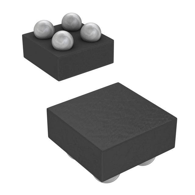
| 产品图片 |
|
| rohs | 符合RoHS无铅 / 符合限制有害物质指令(RoHS)规范要求 |
| 产品系列 | 电源管理 IC,低压差稳压器,Texas Instruments TLV70518YFPR- |
| 数据手册 | |
| 产品型号 | TLV70518YFPR |
| PSRR/纹波抑制—典型值 | 80 dB |
| 产品 | Low Noise LDO Regulator |
| 产品种类 | 低压差稳压器 |
| 供应商器件封装 | 4-DSBGA(0.8x0.8) |
| 其它名称 | 296-30106-6 |
| 包装 | Digi-Reel® |
| 商标 | Texas Instruments |
| 回动电压—最大值 | 250 mV |
| 安装类型 | 表面贴装 |
| 安装风格 | SMD/SMT |
| 封装 | Reel |
| 封装/外壳 | 4-XFBGA,DSBGA |
| 封装/箱体 | DSBGA-4 |
| 工作温度 | -40°C ~ 125°C |
| 工厂包装数量 | 3000 |
| 最大功率耗散 | 714 mW |
| 最大工作温度 | + 125 C |
| 最大输入电压 | 6 V |
| 最小工作温度 | - 40 C |
| 最小输入电压 | 2 V |
| 标准包装 | 1 |
| 电压-跌落(典型值) | - |
| 电压-输入 | 2 V ~ 5.5 V |
| 电压-输出 | 1.8V |
| 电压调节准确度 | 0.5 % |
| 电流-输出 | 200mA |
| 电流-限制(最小值) | 260mA |
| 稳压器拓扑 | 正,固定式 |
| 稳压器数 | 1 |
| 类型 | Linear LDO Regulator |
| 系列 | TLV70518 |
| 线路调整率 | 0.05 mV |
| 负载调节 | 1 mV |
| 输出电压 | 1.8 V |
| 输出电流 | 200 mA |
| 输出端数量 | 1 Output |
| 输出类型 | Fixed |


- 商务部:美国ITC正式对集成电路等产品启动337调查
- 曝三星4nm工艺存在良率问题 高通将骁龙8 Gen1或转产台积电
- 太阳诱电将投资9.5亿元在常州建新厂生产MLCC 预计2023年完工
- 英特尔发布欧洲新工厂建设计划 深化IDM 2.0 战略
- 台积电先进制程称霸业界 有大客户加持明年业绩稳了
- 达到5530亿美元!SIA预计今年全球半导体销售额将创下新高
- 英特尔拟将自动驾驶子公司Mobileye上市 估值或超500亿美元
- 三星加码芯片和SET,合并消费电子和移动部门,撤换高东真等 CEO
- 三星电子宣布重大人事变动 还合并消费电子和移动部门
- 海关总署:前11个月进口集成电路产品价值2.52万亿元 增长14.8%


PDF Datasheet 数据手册内容提取
Product Order Technical Tools & Support & Folder Now Documents Software Community TLV705,TLV705P SBVS151F–DECEMBER2010–REVISEDAPRIL2017 TLV705 200-mA, Low I , Low-Noise, Low-Dropout Regulator in Ultra-Small, Q 0.77-mm × 0.77-mm DSBGA and PicoStar™ 1 Features 3 Description • VeryLowDropout: The TLV705 series of low-dropout (LDO) linear 1 regulators are low quiescent current devices with – 105mVatI =150mA OUT excellent line and load transient performance. These – 145mVatI =200mA devices are designed for power-sensitive OUT • Accuracy:0.5%Typical applications, with a precision band gap. An error amplifier provides typical accuracy of 0.5%. Low • LowI :35μA Q output noise, very high power-supply rejection ratio • AvailableinFixed-OutputVoltagesFrom (PSRR), and low dropout voltage make this series of 0.7Vto4.8V LDOs ideal for a wide selection of battery-operated • V Range:2Vto5.5V handheld equipment. All devices have a thermal IN shutdownandcurrentlimitforsafety. • HighPSRR:70dBat1kHz • StableWithEffectiveCapacitanceof0.1 μF Furthermore, the TLV705 series is stable with an effective output capacitance of only 0.1 μF. This • ThermalShutdownandOvercurrentProtection feature enables the use of cost-effective capacitors • AvailableinanUltra-LowProfile(0.15-mm that have higher bias voltage and temperature MaximumHeight)PicoStarPackageOption derating. The devices regulate to the specified accuracy with zero output load. The TLV705P series 2 Applications also provides an active pulldown circuit to quickly dischargeoutput. • WirelessHandsets • SmartPhones The TLV705 and TLV705P series are both available in 0.77-mm × 0.77-mm DSBGA and PicoStar • Zigbee®Networks packages with three height options that are optimal • Bluetooth®Devices forhandheldapplications. • OtherLi-IonOperatedHandheldProducts DeviceInformation(1) • WLANandOtherPCAdd-OnCards PARTNUMBER PACKAGE BODYSIZE(NOM) DSGBA(4) 0.77mm×0.77mm TLV705 PicoStar(4) 0.77mm×0.77mm (1) For all available packages, see the orderable addendum at theendofthedatasheet. TypicalApplicationCircuit(Fixed-VoltageVersions) Input V V Output IN OUT 1 mF C C IN OUT Ceramic TLV705 On Off EN GND Copyright © 2017,Texas Instruments Incorporated 1 An IMPORTANT NOTICE at the end of this data sheet addresses availability, warranty, changes, use in safety-critical applications, intellectualpropertymattersandotherimportantdisclaimers.PRODUCTIONDATA.
TLV705,TLV705P SBVS151F–DECEMBER2010–REVISEDAPRIL2017 www.ti.com Table of Contents 1 Features.................................................................. 1 8.2 TypicalApplication..................................................15 2 Applications........................................................... 1 8.3 Do'sandDon'ts.......................................................16 3 Description............................................................. 1 9 PowerSupplyRecommendations...................... 16 4 RevisionHistory..................................................... 2 10 Layout................................................................... 17 5 PinConfigurationandFunctions......................... 4 10.1 LayoutGuidelines.................................................17 10.2 LayoutExample....................................................17 6 Specifications......................................................... 5 10.3 PowerDissipation.................................................17 6.1 AbsoluteMaximumRatings .....................................5 10.4 PowerDissipationandJunctionTemperature......17 6.2 ESDRatings ............................................................5 10.5 EstimatingJunctionTemperature.........................18 6.3 RecommendedOperatingConditions.......................5 11 DeviceandDocumentationSupport................. 19 6.4 ThermalInformation..................................................5 6.5 ElectricalCharacteristics...........................................6 11.1 DeviceSupport ....................................................19 6.6 TypicalCharacteristics..............................................7 11.2 DocumentationSupport .......................................19 11.3 RelatedLinks........................................................19 7 DetailedDescription............................................ 12 11.4 CommunityResources..........................................20 7.1 Overview.................................................................12 11.5 Trademarks...........................................................20 7.2 FunctionalBlockDiagrams.....................................12 11.6 ElectrostaticDischargeCaution............................20 7.3 FeatureDescription.................................................13 11.7 Glossary................................................................20 7.4 DeviceFunctionalModes........................................14 12 Mechanical,Packaging,andOrderable 8 ApplicationandImplementation........................ 15 Information........................................................... 20 8.1 ApplicationInformation............................................15 12.1 PackageMounting................................................20 4 Revision History NOTE:Pagenumbersforpreviousrevisionsmaydifferfrompagenumbersinthecurrentversion. ChangesfromRevisionE(May2015)toRevisionF Page • Deleted"x"fromTLV705deviceindocumenttitle ................................................................................................................ 1 • Changedpackagedimensionsindocumenttitlefrom"0.8-mm×0.8-mm"to"0.77-mm×0.77-mm" .................................. 1 • Changedultra-lowprofilemaximumheightfrom0.2-mmto0.15-mminApplicationssection ............................................. 1 • ChangedpackagedimensionsinDescriptionsectionfrom0.8-mmto0.77-mm................................................................... 1 • ChangedDSBGApackagedimensionsfrom"0.80mm×0.80mm"to"0.77mm×0.77mm"intheDevice Informationtable .................................................................................................................................................................... 1 • AddedcopyrightstatementtotheTypicalApplicationCircuit ............................................................................................... 1 • ChangedformattingofThermalInformationtablenote ......................................................................................................... 5 • Deleted"x"fromdevicenumberinThermalInformationtable .............................................................................................. 5 • AddedcopyrightstatementtofunctionalblockdiagramsinFunctionalBlockDiagramssection........................................ 12 • AddedcopyrightstatementtoTypicalApplicationCircuit(Fixed-VoltageVersions)intheTypicalApplicationsection .....15 • ChangedformattingofdocumentreferenceinRelatedDocumentationsection ................................................................. 19 • Changedtableheadertitlefrom"Sample&Buy"to"OrderNow"intheRelatedLinkstable ............................................ 19 ChangesfromRevisionD(April2015)toRevisionE Page • Addednewpackage(YFM)todocument .............................................................................................................................. 1 • AddedPicoStartotitle ........................................................................................................................................................... 1 • ChangedlastFeaturesbullet................................................................................................................................................. 1 • ChangedlastsentenceofDescriptionsection ...................................................................................................................... 1 • AddedsecondrowtoDeviceInformationtable ..................................................................................................................... 1 • AddedYFMpinoutdrawing................................................................................................................................................... 4 • AddedYFMpackagetoThermalInformationtable ............................................................................................................... 5 • ChangedV parameterunitsinElectricalCharacteristicstable:%forfirstrow,mVforsecondrow.................................... 6 O 2 SubmitDocumentationFeedback Copyright©2010–2017,TexasInstrumentsIncorporated ProductFolderLinks:TLV705 TLV705P
TLV705,TLV705P www.ti.com SBVS151F–DECEMBER2010–REVISEDAPRIL2017 • ChangedfirstsentenceofOverviewsection:removednew ............................................................................................... 12 • ChangedfifthsentenceofInternalCurrentLimitsectiontoclarifydescriptionoftheshutdowncircuitfunctionality ..........13 • ChangedVµstoV/µsinsecondparagraphofStart-UpCurrentsection ............................................................................ 13 • Changedittothestart-upcurrentinthirdparagraphofStart-UpCurrentsection .............................................................. 13 • ChangedINPUTtoV inPowerSupplyRecommendationssection.................................................................................. 16 IN • AddedRelatedLinkssection ............................................................................................................................................... 19 • AddedYFMpackagetoPackageMountingsection ........................................................................................................... 20 ChangesfromRevisionC(October2012)toRevisionD Page • AddedESDRatingstable,FeatureDescriptionsection,DeviceFunctionalModes,ApplicationandImplementation section,PowerSupplyRecommendationssection,Layoutsection,DeviceandDocumentationSupportsection,and Mechanical,Packaging,andOrderableInformationsection ................................................................................................. 1 • AddedFeaturesbulletforV range ...................................................................................................................................... 1 IN • ChangedApplicationslistitems............................................................................................................................................. 1 • DeletedPowerDissipationRatingstable .............................................................................................................................. 5 • Changedy-axisunitmeasurementfromI toI forFigure11............................................................................................ 7 LIM CL • ChangedFigure31anddeletedlayoutsilkscreenimages;replacedwithimageofPCBlayoutdrawing........................... 17 • ChangedtitleforFigure31 .................................................................................................................................................. 17 • ChangedtitleofThermalProtectionsection ....................................................................................................................... 17 ChangesfromRevisionB(December2011)toRevisionC Page • DeletedlastFeaturesbullet.................................................................................................................................................... 1 ChangesfromRevisionA(August2011)toRevisionB Page • AddedlastFeaturesbullet...................................................................................................................................................... 1 • ChangedlastsentenceofDescriptionsection....................................................................................................................... 1 • AddedMechanicalPackagessection(removedJune2013;packagesarenowautomaticallyappended)........................... 1 • AddedYFPtotitleofpinoutdrawing..................................................................................................................................... 4 • AddedYFPpackagetoThermalInformationtable................................................................................................................ 5 Copyright©2010–2017,TexasInstrumentsIncorporated SubmitDocumentationFeedback 3 ProductFolderLinks:TLV705 TLV705P
TLV705,TLV705P SBVS151F–DECEMBER2010–REVISEDAPRIL2017 www.ti.com 5 Pin Configuration and Functions YFF,YFPPackages YFMPackage 4-PinDSBGA 4-PinPicoStar TopView TopView EN VIN EN VIN 2 2 GND VOUT GND VOUT 1 1 A B A B PinFunctions PIN I/O DESCRIPTION NAME NO. GND A1 — Groundpin. Enablepin. EN A2 I DrivingENover0.9Vturnsontheregulator.DrivingENbelow0.4Vplacestheregulatorinto shutdownmode,whichreducestheoperatingcurrentto1μA(nominal). Regulatedoutputvoltagepin. V B1 O Placingasmall1-μFceramiccapacitorisrequiredfromthispintogroundtoensurestability. OUT SeeInputandOutputCapacitorRequirementsformoredetails. Inputpin. V B2 I TIrecommendsplacingasmall1-µFcapacitorfromthispintogroundforgoodtransientperformance. IN SeeInputandOutputCapacitorRequirementsformoredetails. 4 SubmitDocumentationFeedback Copyright©2010–2017,TexasInstrumentsIncorporated ProductFolderLinks:TLV705 TLV705P
TLV705,TLV705P www.ti.com SBVS151F–DECEMBER2010–REVISEDAPRIL2017 6 Specifications 6.1 Absolute Maximum Ratings specifiedatT =–40°Cto+125°C,unlessotherwisenoted.AllvoltagesarewithrespecttoGND.(1) J MIN MAX UNIT V –0.3 6 V IN Voltage(2) V –0.3 6 V EN V –0.3 6 V OUT Maximumoutputcurrent I Internallylimited OUT Outputshort-circuitduration Indefinite Operatingjunction,T –55 150 °C J Temperature Storage,T –55 150 °C stg (1) StressesbeyondthoselistedunderAbsoluteMaximumRatingsmaycausepermanentdamagetothedevice.Thesearestressratings only,andfunctionaloperationofthedeviceattheseoranyotherconditionsbeyondthoseindicatedunderRecommendedOperating Conditionsisnotimplied.Exposuretoabsolute-maximum-ratedconditionsforextendedperiodsmyaffectdevicereliability. (2) Allvoltagesarewithrespecttonetworkgroundpin. 6.2 ESD Ratings VALUE UNIT Humanbodymodel(HBM),perANSI/ESDA/JEDECJS-001(1) ±2000 V Electrostaticdischarge V (ESD) Chargeddevicemodel(CDM),perJEDECspecificationJESD22-C101(2) ±500 (1) JEDECdocumentJEP155statesthat500-VHBMallowssafemanufacturingwithastandardESDcontrolprocess. (2) JEDECdocumentJEP157statesthat250-VCDMallowssafemanufacturingwithastandardESDcontrolprocess. 6.3 Recommended Operating Conditions overoperatingjunctiontemperaturerange(unlessotherwisenoted) MIN NOM MAX UNIT V Inputvoltage 2 5.5 V IN V Outputvoltage 0.7 4.8 V OUT I Outputcurrent 0 200 mA OUT T Junctiontemperature –40 125 °C J 6.4 Thermal Information TLV705 THERMALMETRIC(1) YFF,YFP YFM UNIT (DSBGA) (PicoStar) 4PINS 4PINS R Junction-to-ambientthermalresistance 160 191.7 °C/W θJA R Junction-to-case(top)thermalresistance 80 3.1 °C/W θJC(top) R Junction-to-boardthermalresistance 90 36.5 °C/W θJB ψ Junction-to-topcharacterizationparameter 0.5 2.8 °C/W JT ψ Junction-to-boardcharacterizationparameter 78 26.5 °C/W JB (1) Formoreinformationabouttraditionalandnewthermalmetrics,seetheSemiconductorandICPackageThermalMetricsapplication report. Copyright©2010–2017,TexasInstrumentsIncorporated SubmitDocumentationFeedback 5 ProductFolderLinks:TLV705 TLV705P
TLV705,TLV705P SBVS151F–DECEMBER2010–REVISEDAPRIL2017 www.ti.com 6.5 Electrical Characteristics atT =–40°Cto+125°C,V =V +0.5Vor2V(whicheverisgreater),I =10mA,V =0.9V,and J IN OUT(nom) OUT EN C =1μF,unlessotherwisenoted.TypicalvaluesareatT =25°C. OUT J PARAMETER TESTCONDITIONS MIN TYP MAX UNIT V Inputvoltagerange 2 5.5 V IN V Outputvoltagerange 0.7 4.8 V OUT 0mA≤I ≤200mA,V ≥1V –2% ±0.5% 2% OUT OUT V DCoutputaccuracy –40°C≤T ≤125°C O J 0mA≤I ≤200mA,V <1V –20 ±5 20 mV OUT OUT ΔV Lineregulation V +0.5V≤V ≤5.5V 0.05 5 mV OUT(ΔVIN) OUT(nom) IN ΔV Loadregulation 0mA≤I ≤200mA 1 mV OUT(ΔIOUT) OUT V Dropoutvoltage(1) V =0.98×V ,I =200mA 145 250 mV DO IN OUT(nom) OUT I Outputcurrentlimit V =0.9×V ,T =25°C 260 400 550 mA CL OUT OUT(nom) J I =0mA 35 55 μA OUT I Groundpincurrent GND I =200mA 315 μA OUT Shutdowngroundpin I V ≤0.4V,2V≤V ≤4.5V 1 1.8 μA SHUTDOWN current EN IN V =2.3V,V =1.8V,I =10mA, IN OUT OUT 80 dB Power-supply f=10kHz PSRR rejectionratio V =2.3V,V =1.8V,I =10mA, IN OUT OUT 55 dB f=1MHz V =2.3V,V =1.8V 26.6 μV IN OUT RMS BW=100Hzto V =3.3V,V =2.8V 26.7 μV 100kHz,I =10mA IN OUT RMS OUT V =3.8V,V =3.3V 28.2 μV IN OUT RMS V Outputnoisevoltage n V =2.3V,V =1.8V 30.7 μV IN OUT RMS BW=10Hzto100kHz, V =3.3V,V =2.8V 31.3 μV I =10mA IN OUT RMS OUT V =3.8V,V =3.3V 34.1 μV IN OUT RMS t Start-uptime(2) C =1μF,I =200mA 100 μs STR OUT OUT V Enablehigh(enabled) 0.9 V V HI IN V Enablelow(disabled) 0 0.4 V LO I ENpincurrent V =5.5V 0.01 μA EN EN UVLO Undervoltagelockout V rising 1.9 V IN Thermalshutdown Shutdown,temperatureincreasing 160 °C t SD temperature Reset,temperaturedecreasing 140 °C Operatingjunction T –40 125 °C J temperature (1) V ismeasuredfordeviceswithV =2.35VsothatV =2.3V. DO OUT(nom) IN (2) Start-uptime=timefromENassertionto0.98×V . OUT(nom) 6 SubmitDocumentationFeedback Copyright©2010–2017,TexasInstrumentsIncorporated ProductFolderLinks:TLV705 TLV705P
TLV705,TLV705P www.ti.com SBVS151F–DECEMBER2010–REVISEDAPRIL2017 6.6 Typical Characteristics overoperatingtemperaturerange(T =–40°Cto+125°C),I =10mA,V =0.9V,C =1μF,andV =V + J OUT EN OUT IN OUT(nom) 0.5Vor2V,whicheverisgreater,unlessotherwisenoted.TypicalvaluesareatT =25°C. J 1.90 1.90 V = 1.8 V V = 1.8 V 1.88 OUT 1.88 OUT I = 10 mA I = 200 mA OUT OUT 1.86 1.86 1.84 1.84 V) 1.82 V) 1.82 (UT 1.80 (UT 1.80 O O V 1.78 V 1.78 1.76 +125°C 1.76 +125°C 1.74 +85°C 1.74 +85°C +25°C +25°C 1.72 -40°C 1.72 -40°C 1.70 1.70 2.1 2.6 3.1 3.6 4.1 4.6 5.1 5.6 2.1 2.6 3.1 3.6 4.1 4.6 5.1 5.6 V (V) V (V) IN IN Figure1.LineRegulation Figure2.LineRegulation 1.90 250 1.88 VOUT= 1.8 V IOUT= 200 mA 1.86 200 1.84 V) 1.82 V) 150 ( m VOUT 11..8708 V(DO 100 1.76 +125°C +125°C 1.74 +85°C 50 +85°C +25°C +25°C 1.72 -40°C -40°C 1.70 0 0 50 100 150 200 2 2.25 2.5 2.75 3 3.25 3.5 3.75 4 4.25 4.5 4.75 I (mA) V (V) OUT IN Figure3.LoadRegulation(0mA≤I ≤200mA) Figure4.DropoutVoltagevsInputVoltage OUT 140 1.90 VOUT= 4.8 V 1.88 VOUT= 1.8 V 120 1.86 100 1.84 V) 80 V) 1.82 m ( V(DO 60 VOUT 11..8708 40 +125°C 1.76 +85°C 1.74 10mA 20 +25°C 150mA 1.72 -40°C 200mA 0 1.70 0 50 100 150 200 -40 -25 -10 5 20 35 50 65 80 95 110 125 I (mA) Temperature (°C) OUT Figure5.DropoutVoltagevsOutputCurrent Figure6.OutputVoltagevsTemperature Copyright©2010–2017,TexasInstrumentsIncorporated SubmitDocumentationFeedback 7 ProductFolderLinks:TLV705 TLV705P
TLV705,TLV705P SBVS151F–DECEMBER2010–REVISEDAPRIL2017 www.ti.com Typical Characteristics (continued) overoperatingtemperaturerange(T =–40°Cto+125°C),I =10mA,V =0.9V,C =1μF,andV =V + J OUT EN OUT IN OUT(nom) 0.5Vor2V,whicheverisgreater,unlessotherwisenoted.TypicalvaluesareatT =25°C. J 50 400 V = 1.8 V OUT V = 1.8 V 45 OUT I = 0 mA 350 OUT 40 300 35 250 A) 30 A) m m ( 25 ( 200 D D N N IG 20 IG 150 15 +125°C +125°C 100 10 +85°C +85°C +25°C 50 +25°C 5 -40°C -40°C 0 0 2.3 2.7 3.1 3.5 3.9 4.3 4.7 5.1 5.5 0 50 100 150 200 V (V) I (mA) IN OUT Figure7.GroundPinCurrentvsInputVoltage Figure8.GroundPinCurrentvsOutputCurrent 50 2.5 45 VOUT= 1.8 V VOUT= 1.8 V I = 0 mA OUT 40 2 35 A) 30 A) 1.5 I(mGND 2250 I(mSHDN 1 15 +125°C 10 0.5 +85°C +25°C 5 -40°C 0 0 -40 -25 -10 5 20 35 50 65 80 95 110 125 2.3 2.7 3.1 3.5 3.9 4.3 4.7 5.1 5.5 Temperature (°C) V (V) IN Figure9.GroundPinCurrentvsTemperature Figure10.ShutdownPinCurrentvsInputVoltage 500 100 V = 1.8 V V = 2.3 V OUT 90 IN V = 1.8 V OUT 470 80 70 (mA) 440 +25°C R (dB) 6500 ICL 410 PSR 40 30 380 20 I =10 mA 10 OUT I = 150 mA OUT 350 0 2.5 3 3.5 4 4.5 5 5.5 10 100 1k 10k 100k 1M 10M V (V) Frequency (Hz) IN Figure11.CurrentLimitvsInputVoltage Figure12.Power-SupplyRejectionRatiovsFrequency 8 SubmitDocumentationFeedback Copyright©2010–2017,TexasInstrumentsIncorporated ProductFolderLinks:TLV705 TLV705P
TLV705,TLV705P www.ti.com SBVS151F–DECEMBER2010–REVISEDAPRIL2017 Typical Characteristics (continued) overoperatingtemperaturerange(T =–40°Cto+125°C),I =10mA,V =0.9V,C =1μF,andV =V + J OUT EN OUT IN OUT(nom) 0.5Vor2V,whicheverisgreater,unlessotherwisenoted.TypicalvaluesareatT =25°C. J 100 10 90 VOUT= 1.8 V H)z VOUT= 1.8 V Ö V/ 80 m y ( 1 70 sit n R (dB) 6500 se De 0.1 R oi PS 40 al N 30 ctr 20 1 kHz Spe 0.01 10 kHz ut 10 p 100 kHz ut 0 O 0 2.1 2.2 2.3 2.4 2.5 2.6 2.7 2.8 10 100 1 k 10 k 100 k 1 M 10 M Input Voltage (V) Frequency (Hz) Figure13.Power-SupplyRejectionRatiovsInputVoltage Figure14.OutputSpectralNoiseDensityvsFrequency 45 t = t = 1ms R F 40 )S 35 M mVR 30 VOUT e ( (20 mV/div) s 25 oi N d 20 200 mA e grat 15 e nt 10 (100 mA/div) I Bandwidth: 100 Hz to 100 kHz IOUT 0 mA 5 Bandwidth: 10 Hz to 100 kHz 0 0.8 1.2 1.6 2 2.4 2.8 3.2 3.6 4 4.4 4.8 Time (200ms/div) V (V) OUT Figure15.IntegratedNoisevsOutputVoltage Figure16.LoadTransient0 t = t = 1ms t = t = 1ms R F R F V OUT (20 mV/div) V OUT (20 mV/div) 200 mA 100 mA I (50 mA/div) OUT (100 mA/div) IOUT 1 mA 1 mA Time (200ms/div) Time (200ms/div) Figure17.LoadTransient1 Figure18.LoadTransient3 Copyright©2010–2017,TexasInstrumentsIncorporated SubmitDocumentationFeedback 9 ProductFolderLinks:TLV705 TLV705P
TLV705,TLV705P SBVS151F–DECEMBER2010–REVISEDAPRIL2017 www.ti.com Typical Characteristics (continued) overoperatingtemperaturerange(T =–40°Cto+125°C),I =10mA,V =0.9V,C =1μF,andV =V + J OUT EN OUT IN OUT(nom) 0.5Vor2V,whicheverisgreater,unlessotherwisenoted.TypicalvaluesareatT =25°C. J 2.9 V Slew Rate = 1 V/ms 2.9 V Slew Rate = 1 V/ms V V IN IN (200 mV/div) (200 mV/div) 2.3 V 2.3 V V V (5 mV/div) OUT (5 mV/div) OUT Time (100ms/div) Time (100ms/div) Figure19.Small-StepLineTransient(10mA) Figure20.Small-StepLineTransient(200mA) I = 0 mA I = 200 mA OUT OUT C2 C2 (1 V/div) (1 V/div) C1 C1 (1 V/div) (1 V/div) C4 (100 mA/div) C4 (100 mA/div) Time (50ms/div) Time (10ms/div) Figure21.V InrushCurrent Figure22.V InrushCurrent IN IN Slew Rate = 1 V/ms 5.5 V 5.5 V (2 V/div) (2 V/div) VIN 2.3 V VIN 2.3 V V V (5 mV/div) OUT (5 mV/div) OUT Slew Rate = 1 V/ms Time (100ms/div) Time (100ms/div) Figure23.LineTransient(10mA) Figure24.LineTransient(200mA) 10 SubmitDocumentationFeedback Copyright©2010–2017,TexasInstrumentsIncorporated ProductFolderLinks:TLV705 TLV705P
TLV705,TLV705P www.ti.com SBVS151F–DECEMBER2010–REVISEDAPRIL2017 Typical Characteristics (continued) overoperatingtemperaturerange(T =–40°Cto+125°C),I =10mA,V =0.9V,C =1μF,andV =V + J OUT EN OUT IN OUT(nom) 0.5Vor2V,whicheverisgreater,unlessotherwisenoted.TypicalvaluesareatT =25°C. J V IN (1 V/div) V OUT Time (100ms/div) Figure25.Power-UpandPower-Down Copyright©2010–2017,TexasInstrumentsIncorporated SubmitDocumentationFeedback 11 ProductFolderLinks:TLV705 TLV705P
TLV705,TLV705P SBVS151F–DECEMBER2010–REVISEDAPRIL2017 www.ti.com 7 Detailed Description 7.1 Overview The TLV705 and TLV705P series of devices belong to a family of next-generation value low-dropout (LDO) voltage regulators. These devices consume low quiescent current and deliver excellent line and load transient performance. This performance, combined with low noise, very good PSRR with little (V – V ) headroom, IN OUT makes these devices ideal for RF portable applications. This family of regulators offers sub-band-gap output voltages down to 0.7 V, current limit, and thermal protection, and are specified from –40°C to +125°C. The TLV705Pprovidesanactivepulldowncircuittoquicklydischargetheoutputs. 7.2 Functional Block Diagrams V V IN OUT Current Limit Thermal Shutdown UVLO EN Bandgap LOGIC TLV705 Series GND Copyright © 2017,Texas Instruments Incorporated Figure26. TLV705Series TLV705PSeries V V IN OUT Current Limit Thermal Shutdown 120Ω UVLO EN Bandgap LOGIC GND Copyright © 2017,Texas Instruments Incorporated Figure27. TLV705PSeries 12 SubmitDocumentationFeedback Copyright©2010–2017,TexasInstrumentsIncorporated ProductFolderLinks:TLV705 TLV705P
TLV705,TLV705P www.ti.com SBVS151F–DECEMBER2010–REVISEDAPRIL2017 7.3 Feature Description 7.3.1 InternalCurrentLimit The internal current limits of the TLV705 series help protect the regulator during fault conditions. During current limit, the output sources a fixed amount of current that is largely independent of output voltage. In such a case, the output voltage is not regulated, and can be measured as V = I × R . The PMOS pass transistor OUT LIMIT LOAD dissipates [(V – V ) × I ] until a thermal shutdown is triggered and the device turns off. When the device IN OUT LIMIT cools down, the internal thermal shutdown circuit turns the device back on. If the fault condition continues, the device cycles between current limit and thermal shutdown; see Power Dissipation and Junction Temperature for moredetails. The PMOS pass element in the TLV705 has a built-in body diode that conducts current when the voltage at V OUT exceeds the voltage at V . This current is not limited, so if extended reverse voltage operation is anticipated, TI IN recommendsexternallimitingto5%oftheratedoutputcurrent. 7.3.2 UndervoltageLockout(UVLO) TheTLV705usesanUVLOcircuittokeeptheoutputshutoffuntiltheinternalcircuitryisoperatingproperly. 7.3.3 Start-UpCurrent The TLV705 uses a unique start-up architecture that creates a constant start-up time regardless of the output capacitor. The start-up current is given by Equation 1. Equation 1 shows that start-up current is directly proportionaltoC . OUT I =C (μF)×0.06(Vμs)+I (mA) (1) STARTUP OUT LOAD TheoutputvoltageramprateisindependentofC andtheloadcurrent,andhasatypicalvalueof0.06V/μs. OUT The TLV705 automatically adjusts the soft-start current to supply both the load current and the current to charge C . For example, if I = 0 mA upon enabling the LDO, then I = 1 μF × 0.06 Vμs + 0 mA = 60 mA, OUT LOAD STARTUP whichisthecurrentthatchargestheoutputcapacitor. However,ifI =200mA,thenI =1 μF× 0.06V/ μs+200mA=260mA,whichistherequiredcurrent LOAD STARTUP tochargetheoutputcapacitorandsupplytheloadcurrent. If the output capacitor and load increase such that the start-up current exceeds the output current limit, the start- up current is clamped at the typical current limit of 400 mA. For example, if C = 10 μF and OUT I =200mA,then10μF×0.06V/ μs+200mA=800mAisnotsuppliedandisinsteadclampedat400mA. OUT 7.3.4 DropoutVoltage The TLV705 uses a PMOS pass transistor to achieve low dropout. When (V – V ) is less than the dropout IN OUT voltage (V ), the PMOS pass device is in the linear region of operation and the input-to-output resistance is the DO R of the PMOS pass element. V approximately scales with the output current because the PMOS device DS(on) DO functionsasaresistorindropout. As with any linear regulator, PSRR and transient response are degraded as (V – V ) approaches dropout. IN OUT ThiseffectisshowninFigure13intheTypicalCharacteristics. 7.3.5 Shutdown The enable pin (EN) is active high. The device is enabled when the EN pin goes above 0.9 V. This relatively lower value of voltage required to turn the LDO on can power the device with the GPIO of recent processors with a GPIO voltage lower than traditional microcontrollers. The device is turned off when the EN pin is held at less than 0.4 V. When shutdown capability is not required, EN can be connected to the V pin. The TLV705P version IN hasinternalactivepulldowncircuitrythatdischargestheoutputwithatimeconstantof: τ=(120×R )/(120+R )×C L L OUT where • R =loadresistance L • C =outputcapacitor (2) OUT Copyright©2010–2017,TexasInstrumentsIncorporated SubmitDocumentationFeedback 13 ProductFolderLinks:TLV705 TLV705P
TLV705,TLV705P SBVS151F–DECEMBER2010–REVISEDAPRIL2017 www.ti.com 7.4 Device Functional Modes 7.4.1 NormalOperation Thedeviceregulatestothenominaloutputvoltageunderthefollowingconditions: • Theinputvoltageisgreaterthanthenominaloutputvoltageaddedtothedropoutvoltage. • Theoutputcurrentislessthanthecurrentlimit. • TheinputvoltageisgreaterthantheUVLOvoltage. 7.4.2 DropoutOperation If the input voltage is lower than the nominal output voltage plus the specified dropout voltage, but all other conditions are met for normal operation, the device operates in dropout mode. In this condition, the output voltage is the same the input voltage minus the dropout voltage. The transient performance of the device is significantly degraded because the pass device is in a triode state and no longer regulates the output voltage of theLDO.Lineorloadtransientsindropoutcanresultinlargeoutputvoltagedeviations. Table1liststheconditionsthatleadtothedifferentmodesofoperation. Table1.DeviceFunctionalModeComparison PARAMETER OPERATINGMODE V I IN OUT Normalmode V >V +V I <I IN OUT(nom) DO OUT CL Dropoutmode V <V +V I <I IN OUT(nom) DO OUT CL Currentlimit V >UVLO I >I IN OUT CL 14 SubmitDocumentationFeedback Copyright©2010–2017,TexasInstrumentsIncorporated ProductFolderLinks:TLV705 TLV705P
TLV705,TLV705P www.ti.com SBVS151F–DECEMBER2010–REVISEDAPRIL2017 8 Application and Implementation NOTE Information in the following applications sections is not part of the TI component specification, and TI does not warrant its accuracy or completeness. TI’s customers are responsible for determining suitability of components for their purposes. Customers should validateandtesttheirdesignimplementationtoconfirmsystemfunctionality. 8.1 Application Information TheTLV705isaLDOthatoffersverylowdropoutvoltagesinatinypackage.Theoperatingjunctiontemperature ofthisdeviceis–40°Cto+125°C. 8.2 Typical Application Input V V Output IN OUT 1 mF C C IN OUT Ceramic TLV705 On Off EN GND Copyright © 2017,Texas Instruments Incorporated Figure28. TypicalApplicationCircuit(Fixed-VoltageVersions) 8.2.1 DesignRequirements Table2liststhedesignparameters. Table2.DesignParameters PARAMETER DESIGNREQUIREMENT Inputvoltage 2.5Vto3.3V Outputvoltage 1.8V Outputcurrent 100mA 8.2.2 DetailedDesignProcedure Selectthedesireddevicebasedontheoutputvoltage. Provide an input supply with adequate headroom to account for dropout. The input supply must also provide adequatecurrenttoaccountfortheGNDpincurrentandloadcurrent. Copyright©2010–2017,TexasInstrumentsIncorporated SubmitDocumentationFeedback 15 ProductFolderLinks:TLV705 TLV705P
TLV705,TLV705P SBVS151F–DECEMBER2010–REVISEDAPRIL2017 www.ti.com 8.2.2.1 InputandOutputCapacitorRequirements TI recommends using 1-μF X5R- and X7R-type ceramic capacitors because these components have minimal variation in value and equivalent series resistance (ESR) over temperature. However, the TLV705 series is designed to be stable with an effective capacitance of 0.1 μF or larger at the output. As a result, the device is stable with capacitors of other dielectrics as long as the effective capacitance under the operating bias voltage and temperature is greater than 0.1 μF. This effective capacitance refers to the capacitance that the LDO detects under operating bias voltage and temperature conditions (that is, the capacitance after taking the bias voltage andtemperaturederatingintoconsideration).Inadditiontoallowingtheuseoflowercostdielectrics,theeffective capacitance enables using smaller footprint capacitors that have higher derating in space-constrained applications. Using a 0.1-μF rating capacitor at the output of the LDO does not ensure stability because the effective capacitanceunderoperatingconditionsislessthan0.1 μF.MaximumESRmustbelessthan200mΩ. Although an input capacitor is not required for stability, good analog design practice is to connect a 0.1-μF to 1-μF low ESR capacitor across the V and GND pins of the regulator. This capacitor counteracts reactive input IN sources and improves transient response, noise rejection, and ripple rejection. A higher-value capacitor can be necessary if large, fast rise-time load transients are anticipated, or if the device is not located close to the power source.Ifsourceimpedanceismorethan2Ω,a0.1-μFinputcapacitormaybenecessarytoensurestability. 8.2.2.2 TransientResponse As with any regulator, increasing the size of the output capacitor reduces overshoot and undershoot magnitude, butincreasesthedurationofthetransientresponse. 8.2.3 ApplicationCurves 100 V = 2.3 V 90 IN V = 1.8 V OUT 80 70 VIN B) 60 d R ( 50 (1 V/div) R S 40 P 30 VOUT 20 I =10 mA 10 OUT I = 150 mA OUT 0 10 100 1k 10k 100k 1M 10M Time (100ms/div) Frequency (Hz) Figure29.Power-SupplyRejectionRatiovsFrequency Figure30.Power-UpandPower-Down 8.3 Do's and Don'ts Placeinputandoutputcapacitorsascloseaspossibletothedevice. Donotexceedthedeviceabsolutemaximumratings. 9 Power Supply Recommendations Connect a low output impedance power supply directly to the V pin of the TLV705. Inductive impedances IN between the input supply and the V pin can create significant voltage excursions at the V pin during start-up IN IN orloadtransientevents. 16 SubmitDocumentationFeedback Copyright©2010–2017,TexasInstrumentsIncorporated ProductFolderLinks:TLV705 TLV705P
TLV705,TLV705P www.ti.com SBVS151F–DECEMBER2010–REVISEDAPRIL2017 10 Layout 10.1 Layout Guidelines Place input and output capacitors as close to the device pins as possible. To improve ac performance (such as PSRR, output noise, and transient response), TI recommends designing the board with the input and output capacitors on opposite sides of the device. In addition, connect the ground connection for the output capacitor directlytotheGNDpinofthedevice.HighESRcapacitorscandegradePSRR. 10.2 Layout Example VIN VOUT CIN COUT N E GND Represents via used for application-specific connections Figure31. ExamplePCBLayout 10.3 Power Dissipation The ability to remove heat from the die is different for each package type, presenting different considerations in the printed-circuit-board (PCB) layout. The PCB area around the device that is free of other components moves the heat from the device to the ambient air. Performance data for JEDEC low and high-K boards are given in Thermal Information. Using heavier copper increases the effectiveness in removing heat from the device. The additionofplatedthrough-holestoheat-dissipatinglayersalsoimprovesthethermaldissipation. See for thermal performance on the TLV705 evaluation module (EVM). The EVM is a 2-layer board with two ouncesofcopperperside. Powerdissipationdependsoninputvoltageandloadconditions.Powerdissipation(P )isequaltotheproductof D theoutputcurrentandthevoltagedropacrosstheoutputpasselement,asshowninEquation3: P =(V –V )×I (3) D IN OUT OUT 10.4 Power Dissipation and Junction Temperature Thermal protection disables the output when the junction temperature rises to approximately 160°C, allowing the device to cool. When the junction temperature cools to approximately 140°C, the output circuitry is enabled again. Depending on power dissipation, thermal resistance, and ambient temperature, the thermal protection circuit can cycle on and off. This cycling limits the dissipation of the regulator, which protects the regulator from damageasaresultofoverheating. For reliable operation, limit junction temperature to 125°C (maximum). To estimate the margin of safety in a completedesign,increasetheambienttemperatureuntilthethermalprotectionistriggered;useworst-caseloads and signal conditions. For good reliability, trigger thermal protection at least 35°C above the maximum expected ambient condition of the particular application. This configuration produces a worst-case junction temperature of 125°Catthehighestexpectedambienttemperatureandworst-caseload. The internal protection circuitry of the TLV705 is designed to protect against overload conditions. Continuously runningtheTLV705intothermalshutdowndegradesdevicereliability. Copyright©2010–2017,TexasInstrumentsIncorporated SubmitDocumentationFeedback 17 ProductFolderLinks:TLV705 TLV705P
TLV705,TLV705P SBVS151F–DECEMBER2010–REVISEDAPRIL2017 www.ti.com 10.5 Estimating Junction Temperature The JEDEC standard now recommends the use of psi (Ψ) thermal metrics to estimate the junction temperatures of the LDO when in-circuit on a typical PCB board application. These metrics are not strictly discussing thermal resistances; rather, these metrics offer practical and relative means of estimating junction temperatures. These psi metrics are determined to be significantly independent of the copper-spreading area. The key thermal metrics (Ψ andΨ )aregiveninThermalInformationandareusedinaccordancewithEquation4. JT JB Y :T =T +Y ´P JT J T JT D Y :T =T +Y ´P JB J B JB D where: • P isthepowerdissipated,asexplainedinThermalInformation. D • T isthetemperatureatthecenter-topofthedevicepackage,and T • T isthePCBsurfacetemperaturemeasured1mmfromthedevicepackageandcenteredonthepackage B edge. (4) 18 SubmitDocumentationFeedback Copyright©2010–2017,TexasInstrumentsIncorporated ProductFolderLinks:TLV705 TLV705P
TLV705,TLV705P www.ti.com SBVS151F–DECEMBER2010–REVISEDAPRIL2017 11 Device and Documentation Support 11.1 Device Support 11.1.1 DevelopmentSupport 11.1.1.1 EvaluationModules An evaluation module (EVM) is available to assist in the initial circuit performance evaluation using the TLV705. TheTLV70533EVM-596evaluationmodule(andrelateduser'sguide)canberequestedattheTIwebsitethrough theproductfoldersorpurchaseddirectlyfromtheTIeStore. 11.1.1.2 SpiceModels Computer simulation of circuit performance using SPICE is often useful when analyzing the performance of analog circuits and systems. A SPICE model for the TLV705 is available through the product folders under Tools &Software. 11.1.2 DeviceNomenclature Table3.AvailableOptions(1) PRODUCT V OUT xx(x)isthenominaloutputvoltage.Foroutputvoltageswitharesolutionof100mV,twodigits areusedintheorderingnumber;otherwise,threedigitsareused(forexample,28=2.8V;475 =4.75V). TLV705xx(x)Pyyyz Pisoptional;deviceswithPhaveanLDOregulatorwithanactiveoutputdischarge. yyyispackagedesignator. zisthepackagequantity.Risforreel(3000pieces),Tisfortape(250pieces). (1) Forthemostcurrentpackageandorderinginformation,seethePackageOptionAddendumattheendofthisdocument,orvisitthe deviceproductfolderatwww.ti.com. 11.2 Documentation Support 11.2.1 RelatedDocumentation • TLV70533EVM-596EvaluationModuleUser'sGuide(SLVU439) 11.3 Related Links The table below lists quick access links. Categories include technical documents, support and community resources,toolsandsoftware,andquickaccesstosampleorbuy. Table4.RelatedLinks TECHNICAL TOOLS& SUPPORT& PARTS PRODUCTFOLDER ORDERNOW DOCUMENTS SOFTWARE COMMUNITY TLV705 Clickhere Clickhere Clickhere Clickhere Clickhere TLV705P Clickhere Clickhere Clickhere Clickhere Clickhere Copyright©2010–2017,TexasInstrumentsIncorporated SubmitDocumentationFeedback 19 ProductFolderLinks:TLV705 TLV705P
TLV705,TLV705P SBVS151F–DECEMBER2010–REVISEDAPRIL2017 www.ti.com 11.4 Community Resources The following links connect to TI community resources. Linked contents are provided "AS IS" by the respective contributors. They do not constitute TI specifications and do not necessarily reflect TI's views; see TI's Terms of Use. TIE2E™OnlineCommunity TI'sEngineer-to-Engineer(E2E)Community.Createdtofostercollaboration amongengineers.Ate2e.ti.com,youcanaskquestions,shareknowledge,exploreideasandhelp solveproblemswithfellowengineers. DesignSupport TI'sDesignSupport QuicklyfindhelpfulE2Eforumsalongwithdesignsupporttoolsand contactinformationfortechnicalsupport. 11.5 Trademarks E2EisatrademarkofTexasInstruments. PicoStarisatrademarkofTexasInstruments,Inc. BluetoothisaregisteredtrademarkofBluetoothSIG,Inc. ZigbeeisaregisteredtrademarkofZigBeeAlliance. Allothertrademarksarethepropertyoftheirrespectiveowners. 11.6 Electrostatic Discharge Caution Thesedeviceshavelimitedbuilt-inESDprotection.Theleadsshouldbeshortedtogetherorthedeviceplacedinconductivefoam duringstorageorhandlingtopreventelectrostaticdamagetotheMOSgates. 11.7 Glossary SLYZ022—TIGlossary. Thisglossarylistsandexplainsterms,acronyms,anddefinitions. 12 Mechanical, Packaging, and Orderable Information The following pages include mechanical, packaging, and orderable information. This information is the most current data available for the designated devices. This data is subject to change without notice and revision of thisdocument.Forbrowser-basedversionsofthisdatasheet,refertotheleft-handnavigation. 12.1 Package Mounting Solder pad footprint recommendations for the TLV705 are available from the Packaging Information page on TI's website through the TLV705 series product folders. The recommended land patterns for the YFF, YFP, and YFM packagesareappendedtothisdatasheet. 20 SubmitDocumentationFeedback Copyright©2010–2017,TexasInstrumentsIncorporated ProductFolderLinks:TLV705 TLV705P
PACKAGE OPTION ADDENDUM www.ti.com 3-Jul-2020 PACKAGING INFORMATION Orderable Device Status Package Type Package Pins Package Eco Plan Lead finish/ MSL Peak Temp Op Temp (°C) Device Marking Samples (1) Drawing Qty (2) Ball material (3) (4/5) (6) TLV705075YFPR ACTIVE DSBGA YFP 4 3000 Green (RoHS SAC396 Level-1-260C-UNLIM -40 to 125 3V & no Sb/Br) TLV705075YFPT ACTIVE DSBGA YFP 4 250 Green (RoHS SAC396 Level-1-260C-UNLIM -40 to 125 3V & no Sb/Br) TLV70509YFPR ACTIVE DSBGA YFP 4 3000 Green (RoHS SAC396 Level-1-260C-UNLIM -40 to 125 3W & no Sb/Br) TLV70509YFPT ACTIVE DSBGA YFP 4 250 Green (RoHS SAC396 Level-1-260C-UNLIM -40 to 125 3W & no Sb/Br) TLV70512YFPR ACTIVE DSBGA YFP 4 3000 Green (RoHS SNAGCU Level-1-260C-UNLIM -40 to 125 BU & no Sb/Br) TLV70512YFPT ACTIVE DSBGA YFP 4 250 Green (RoHS SNAGCU Level-1-260C-UNLIM -40 to 125 BU & no Sb/Br) TLV70515YFPR ACTIVE DSBGA YFP 4 3000 Green (RoHS SNAGCU Level-1-260C-UNLIM -40 to 125 BV & no Sb/Br) TLV70515YFPT ACTIVE DSBGA YFP 4 250 Green (RoHS SNAGCU Level-1-260C-UNLIM -40 to 125 BV & no Sb/Br) TLV705165YFPR ACTIVE DSBGA YFP 4 3000 Green (RoHS SAC396 Level-1-260C-UNLIM -40 to 125 CN & no Sb/Br) TLV705165YFPT ACTIVE DSBGA YFP 4 250 Green (RoHS SAC396 Level-1-260C-UNLIM -40 to 125 CN & no Sb/Br) TLV705185YFPR ACTIVE DSBGA YFP 4 3000 Green (RoHS SNAGCU Level-1-260C-UNLIM -40 to 125 YS & no Sb/Br) TLV705185YFPT ACTIVE DSBGA YFP 4 250 Green (RoHS SAC396 Level-1-260C-UNLIM -40 to 125 YS & no Sb/Br) TLV70518PYFPR ACTIVE DSBGA YFP 4 3000 Green (RoHS SNAGCU Level-1-260C-UNLIM -40 to 125 EV & no Sb/Br) TLV70518PYFPT ACTIVE DSBGA YFP 4 250 Green (RoHS SNAGCU Level-1-260C-UNLIM -40 to 125 EV & no Sb/Br) TLV70518YFMR ACTIVE DSLGA YFM 4 3000 Green (RoHS SNAGCU Level-1-260C-UNLIM -40 to 125 & no Sb/Br) TLV70518YFMT ACTIVE DSLGA YFM 4 250 Green (RoHS SNAGCU Level-1-260C-UNLIM -40 to 125 & no Sb/Br) Addendum-Page 1
PACKAGE OPTION ADDENDUM www.ti.com 3-Jul-2020 Orderable Device Status Package Type Package Pins Package Eco Plan Lead finish/ MSL Peak Temp Op Temp (°C) Device Marking Samples (1) Drawing Qty (2) Ball material (3) (4/5) (6) TLV70518YFPR ACTIVE DSBGA YFP 4 3000 Green (RoHS SNAGCU Level-1-260C-UNLIM -40 to 125 WT & no Sb/Br) TLV70518YFPT ACTIVE DSBGA YFP 4 250 Green (RoHS SNAGCU Level-1-260C-UNLIM -40 to 125 WT & no Sb/Br) TLV70525PYFPR ACTIVE DSBGA YFP 4 3000 Green (RoHS SNAGCU Level-1-260C-UNLIM -40 to 85 EK & no Sb/Br) TLV70525PYFPT ACTIVE DSBGA YFP 4 250 Green (RoHS SNAGCU Level-1-260C-UNLIM -40 to 85 EK & no Sb/Br) TLV70525YFPR ACTIVE DSBGA YFP 4 3000 Green (RoHS SNAGCU Level-1-260C-UNLIM -40 to 125 YB & no Sb/Br) TLV70525YFPT ACTIVE DSBGA YFP 4 250 Green (RoHS SNAGCU Level-1-260C-UNLIM -40 to 125 YB & no Sb/Br) TLV705285YFPR ACTIVE DSBGA YFP 4 3000 Green (RoHS SNAGCU Level-1-260C-UNLIM -40 to 125 BW & no Sb/Br) TLV705285YFPT ACTIVE DSBGA YFP 4 250 Green (RoHS SNAGCU Level-1-260C-UNLIM -40 to 125 BW & no Sb/Br) TLV70528PYFPR ACTIVE DSBGA YFP 4 3000 Green (RoHS SAC396 Level-1-260C-UNLIM -40 to 125 4E & no Sb/Br) TLV70528PYFPT ACTIVE DSBGA YFP 4 250 Green (RoHS SAC396 Level-1-260C-UNLIM -40 to 125 4E & no Sb/Br) TLV70528YFPR ACTIVE DSBGA YFP 4 3000 Green (RoHS SNAGCU Level-1-260C-UNLIM -40 to 125 WU & no Sb/Br) TLV70528YFPT ACTIVE DSBGA YFP 4 250 Green (RoHS SNAGCU Level-1-260C-UNLIM -40 to 125 WU & no Sb/Br) TLV70530YFMR ACTIVE DSLGA YFM 4 3000 Green (RoHS SNAGCU Level-1-260C-UNLIM -40 to 125 & no Sb/Br) TLV70530YFMT ACTIVE DSLGA YFM 4 250 Green (RoHS SNAGCU Level-1-260C-UNLIM -40 to 125 & no Sb/Br) TLV70530YFPR ACTIVE DSBGA YFP 4 3000 Green (RoHS SNAGCU Level-1-260C-UNLIM -40 to 125 XA & no Sb/Br) TLV70530YFPT ACTIVE DSBGA YFP 4 250 Green (RoHS SNAGCU Level-1-260C-UNLIM -40 to 125 XA & no Sb/Br) TLV70533PYFPR ACTIVE DSBGA YFP 4 3000 Green (RoHS SNAGCU Level-1-260C-UNLIM -40 to 125 5L & no Sb/Br) Addendum-Page 2
PACKAGE OPTION ADDENDUM www.ti.com 3-Jul-2020 Orderable Device Status Package Type Package Pins Package Eco Plan Lead finish/ MSL Peak Temp Op Temp (°C) Device Marking Samples (1) Drawing Qty (2) Ball material (3) (4/5) (6) TLV70533PYFPT ACTIVE DSBGA YFP 4 250 Green (RoHS SNAGCU Level-1-260C-UNLIM -40 to 125 5L & no Sb/Br) TLV70533YFFR ACTIVE DSBGA YFF 4 3000 Green (RoHS SNAGCU Level-1-260C-UNLIM -40 to 125 US & no Sb/Br) TLV70533YFFT ACTIVE DSBGA YFF 4 250 Green (RoHS SNAGCU Level-1-260C-UNLIM -40 to 125 US & no Sb/Br) TLV70533YFMR ACTIVE DSLGA YFM 4 3000 Green (RoHS SNAGCU Level-1-260C-UNLIM -40 to 125 & no Sb/Br) TLV70533YFMT ACTIVE DSLGA YFM 4 250 Green (RoHS SNAGCU Level-1-260C-UNLIM -40 to 125 & no Sb/Br) TLV70533YFPR ACTIVE DSBGA YFP 4 3000 Green (RoHS SNAGCU Level-1-260C-UNLIM -40 to 125 VV & no Sb/Br) TLV70533YFPT ACTIVE DSBGA YFP 4 250 Green (RoHS SNAGCU Level-1-260C-UNLIM -40 to 125 VV & no Sb/Br) TLV70534YFPR ACTIVE DSBGA YFP 4 3000 Green (RoHS SNAGCU Level-1-260C-UNLIM -40 to 125 B4 & no Sb/Br) TLV70534YFPT ACTIVE DSBGA YFP 4 250 Green (RoHS SNAGCU Level-1-260C-UNLIM -40 to 125 B4 & no Sb/Br) TLV70536YFMR ACTIVE DSLGA YFM 4 3000 Green (RoHS SNAGCU Level-1-260C-UNLIM -40 to 125 & no Sb/Br) TLV70536YFMT ACTIVE DSLGA YFM 4 250 Green (RoHS SNAGCU Level-1-260C-UNLIM -40 to 125 & no Sb/Br) TLV70536YFPR ACTIVE DSBGA YFP 4 3000 Green (RoHS SNAGCU Level-1-260C-UNLIM -40 to 125 BX & no Sb/Br) TLV70536YFPT ACTIVE DSBGA YFP 4 250 Green (RoHS SNAGCU Level-1-260C-UNLIM -40 to 125 BX & no Sb/Br) (1) The marketing status values are defined as follows: ACTIVE: Product device recommended for new designs. LIFEBUY: TI has announced that the device will be discontinued, and a lifetime-buy period is in effect. NRND: Not recommended for new designs. Device is in production to support existing customers, but TI does not recommend using this part in a new design. PREVIEW: Device has been announced but is not in production. Samples may or may not be available. OBSOLETE: TI has discontinued the production of the device. Addendum-Page 3
PACKAGE OPTION ADDENDUM www.ti.com 3-Jul-2020 (2) RoHS: TI defines "RoHS" to mean semiconductor products that are compliant with the current EU RoHS requirements for all 10 RoHS substances, including the requirement that RoHS substance do not exceed 0.1% by weight in homogeneous materials. Where designed to be soldered at high temperatures, "RoHS" products are suitable for use in specified lead-free processes. TI may reference these types of products as "Pb-Free". RoHS Exempt: TI defines "RoHS Exempt" to mean products that contain lead but are compliant with EU RoHS pursuant to a specific EU RoHS exemption. Green: TI defines "Green" to mean the content of Chlorine (Cl) and Bromine (Br) based flame retardants meet JS709B low halogen requirements of <=1000ppm threshold. Antimony trioxide based flame retardants must also meet the <=1000ppm threshold requirement. (3) MSL, Peak Temp. - The Moisture Sensitivity Level rating according to the JEDEC industry standard classifications, and peak solder temperature. (4) There may be additional marking, which relates to the logo, the lot trace code information, or the environmental category on the device. (5) Multiple Device Markings will be inside parentheses. Only one Device Marking contained in parentheses and separated by a "~" will appear on a device. If a line is indented then it is a continuation of the previous line and the two combined represent the entire Device Marking for that device. (6) Lead finish/Ball material - Orderable Devices may have multiple material finish options. Finish options are separated by a vertical ruled line. Lead finish/Ball material values may wrap to two lines if the finish value exceeds the maximum column width. Important Information and Disclaimer:The information provided on this page represents TI's knowledge and belief as of the date that it is provided. TI bases its knowledge and belief on information provided by third parties, and makes no representation or warranty as to the accuracy of such information. Efforts are underway to better integrate information from third parties. TI has taken and continues to take reasonable steps to provide representative and accurate information but may not have conducted destructive testing or chemical analysis on incoming materials and chemicals. TI and TI suppliers consider certain information to be proprietary, and thus CAS numbers and other limited information may not be available for release. In no event shall TI's liability arising out of such information exceed the total purchase price of the TI part(s) at issue in this document sold by TI to Customer on an annual basis. Addendum-Page 4
PACKAGE MATERIALS INFORMATION www.ti.com 18-Jun-2020 TAPE AND REEL INFORMATION *Alldimensionsarenominal Device Package Package Pins SPQ Reel Reel A0 B0 K0 P1 W Pin1 Type Drawing Diameter Width (mm) (mm) (mm) (mm) (mm) Quadrant (mm) W1(mm) TLV705075YFPR DSBGA YFP 4 3000 180.0 8.4 0.86 0.86 0.59 4.0 8.0 Q1 TLV705075YFPT DSBGA YFP 4 250 180.0 8.4 0.86 0.86 0.59 4.0 8.0 Q1 TLV70509YFPR DSBGA YFP 4 3000 180.0 8.4 0.86 0.86 0.59 4.0 8.0 Q1 TLV70509YFPT DSBGA YFP 4 250 180.0 8.4 0.86 0.86 0.59 4.0 8.0 Q1 TLV70512YFPR DSBGA YFP 4 3000 180.0 8.4 0.86 0.86 0.59 4.0 8.0 Q1 TLV70512YFPT DSBGA YFP 4 250 180.0 8.4 0.86 0.86 0.59 4.0 8.0 Q1 TLV70515YFPR DSBGA YFP 4 3000 180.0 8.4 0.86 0.86 0.59 4.0 8.0 Q1 TLV70515YFPT DSBGA YFP 4 250 180.0 8.4 0.86 0.86 0.59 4.0 8.0 Q1 TLV705165YFPR DSBGA YFP 4 3000 180.0 8.4 0.86 0.86 0.59 4.0 8.0 Q1 TLV705165YFPT DSBGA YFP 4 250 180.0 8.4 0.86 0.86 0.59 4.0 8.0 Q1 TLV705185YFPR DSBGA YFP 4 3000 180.0 8.4 0.86 0.86 0.59 4.0 8.0 Q1 TLV705185YFPT DSBGA YFP 4 250 180.0 8.4 0.86 0.86 0.59 4.0 8.0 Q1 TLV70518PYFPR DSBGA YFP 4 3000 180.0 8.4 0.86 0.86 0.59 4.0 8.0 Q1 TLV70518PYFPT DSBGA YFP 4 250 180.0 8.4 0.86 0.86 0.59 4.0 8.0 Q1 TLV70518YFMR DSLGA YFM 4 3000 180.0 8.4 0.88 0.88 0.22 4.0 8.0 Q1 TLV70518YFMT DSLGA YFM 4 250 180.0 8.4 0.88 0.88 0.22 4.0 8.0 Q1 TLV70518YFPR DSBGA YFP 4 3000 180.0 8.4 0.86 0.86 0.59 4.0 8.0 Q1 TLV70518YFPT DSBGA YFP 4 250 180.0 8.4 0.86 0.86 0.59 4.0 8.0 Q1 PackMaterials-Page1
PACKAGE MATERIALS INFORMATION www.ti.com 18-Jun-2020 Device Package Package Pins SPQ Reel Reel A0 B0 K0 P1 W Pin1 Type Drawing Diameter Width (mm) (mm) (mm) (mm) (mm) Quadrant (mm) W1(mm) TLV70525PYFPR DSBGA YFP 4 3000 180.0 8.4 0.86 0.86 0.59 4.0 8.0 Q1 TLV70525PYFPT DSBGA YFP 4 250 180.0 8.4 0.86 0.86 0.59 4.0 8.0 Q1 TLV70525YFPR DSBGA YFP 4 3000 180.0 8.4 0.86 0.86 0.59 4.0 8.0 Q1 TLV70525YFPT DSBGA YFP 4 250 180.0 8.4 0.86 0.86 0.59 4.0 8.0 Q1 TLV705285YFPR DSBGA YFP 4 3000 180.0 8.4 0.86 0.86 0.59 4.0 8.0 Q1 TLV705285YFPT DSBGA YFP 4 250 180.0 8.4 0.86 0.86 0.59 4.0 8.0 Q1 TLV70528PYFPR DSBGA YFP 4 3000 180.0 8.4 0.86 0.86 0.59 4.0 8.0 Q1 TLV70528PYFPT DSBGA YFP 4 250 180.0 8.4 0.86 0.86 0.59 4.0 8.0 Q1 TLV70528YFPR DSBGA YFP 4 3000 180.0 8.4 0.86 0.86 0.59 4.0 8.0 Q1 TLV70528YFPT DSBGA YFP 4 250 180.0 8.4 0.86 0.86 0.59 4.0 8.0 Q1 TLV70530YFMR DSLGA YFM 4 3000 180.0 8.4 0.88 0.88 0.22 4.0 8.0 Q1 TLV70530YFMT DSLGA YFM 4 250 180.0 8.4 0.88 0.88 0.22 4.0 8.0 Q1 TLV70530YFPR DSBGA YFP 4 3000 180.0 8.4 0.86 0.86 0.59 4.0 8.0 Q1 TLV70530YFPT DSBGA YFP 4 250 180.0 8.4 0.86 0.86 0.59 4.0 8.0 Q1 TLV70533PYFPR DSBGA YFP 4 3000 180.0 8.4 0.86 0.86 0.59 4.0 8.0 Q1 TLV70533PYFPT DSBGA YFP 4 250 180.0 8.4 0.86 0.86 0.59 4.0 8.0 Q1 TLV70533YFFR DSBGA YFF 4 3000 180.0 8.4 0.85 0.85 0.64 4.0 8.0 Q1 TLV70533YFFT DSBGA YFF 4 250 180.0 8.4 0.85 0.85 0.64 4.0 8.0 Q1 TLV70533YFMR DSLGA YFM 4 3000 180.0 8.4 0.88 0.88 0.22 4.0 8.0 Q1 TLV70533YFMT DSLGA YFM 4 250 180.0 8.4 0.88 0.88 0.22 4.0 8.0 Q1 TLV70533YFPR DSBGA YFP 4 3000 180.0 8.4 0.86 0.86 0.59 4.0 8.0 Q1 TLV70533YFPT DSBGA YFP 4 250 180.0 8.4 0.86 0.86 0.59 4.0 8.0 Q1 TLV70534YFPR DSBGA YFP 4 3000 180.0 8.4 0.86 0.86 0.59 4.0 8.0 Q1 TLV70534YFPT DSBGA YFP 4 250 180.0 8.4 0.86 0.86 0.59 4.0 8.0 Q1 TLV70536YFMR DSLGA YFM 4 3000 180.0 8.4 0.88 0.88 0.22 4.0 8.0 Q1 TLV70536YFMT DSLGA YFM 4 250 180.0 8.4 0.88 0.88 0.22 4.0 8.0 Q1 TLV70536YFPR DSBGA YFP 4 3000 180.0 8.4 0.86 0.86 0.59 4.0 8.0 Q1 TLV70536YFPT DSBGA YFP 4 250 180.0 8.4 0.86 0.86 0.59 4.0 8.0 Q1 PackMaterials-Page2
PACKAGE MATERIALS INFORMATION www.ti.com 18-Jun-2020 *Alldimensionsarenominal Device PackageType PackageDrawing Pins SPQ Length(mm) Width(mm) Height(mm) TLV705075YFPR DSBGA YFP 4 3000 182.0 182.0 20.0 TLV705075YFPT DSBGA YFP 4 250 182.0 182.0 20.0 TLV70509YFPR DSBGA YFP 4 3000 182.0 182.0 20.0 TLV70509YFPT DSBGA YFP 4 250 182.0 182.0 20.0 TLV70512YFPR DSBGA YFP 4 3000 182.0 182.0 20.0 TLV70512YFPT DSBGA YFP 4 250 182.0 182.0 20.0 TLV70515YFPR DSBGA YFP 4 3000 182.0 182.0 20.0 TLV70515YFPT DSBGA YFP 4 250 182.0 182.0 20.0 TLV705165YFPR DSBGA YFP 4 3000 182.0 182.0 20.0 TLV705165YFPT DSBGA YFP 4 250 182.0 182.0 20.0 TLV705185YFPR DSBGA YFP 4 3000 182.0 182.0 20.0 TLV705185YFPT DSBGA YFP 4 250 182.0 182.0 20.0 TLV70518PYFPR DSBGA YFP 4 3000 182.0 182.0 20.0 TLV70518PYFPT DSBGA YFP 4 250 182.0 182.0 20.0 TLV70518YFMR DSLGA YFM 4 3000 210.0 185.0 35.0 TLV70518YFMT DSLGA YFM 4 250 210.0 185.0 35.0 TLV70518YFPR DSBGA YFP 4 3000 182.0 182.0 20.0 TLV70518YFPT DSBGA YFP 4 250 182.0 182.0 20.0 TLV70525PYFPR DSBGA YFP 4 3000 182.0 182.0 20.0 TLV70525PYFPT DSBGA YFP 4 250 182.0 182.0 20.0 PackMaterials-Page3
PACKAGE MATERIALS INFORMATION www.ti.com 18-Jun-2020 Device PackageType PackageDrawing Pins SPQ Length(mm) Width(mm) Height(mm) TLV70525YFPR DSBGA YFP 4 3000 182.0 182.0 20.0 TLV70525YFPT DSBGA YFP 4 250 182.0 182.0 20.0 TLV705285YFPR DSBGA YFP 4 3000 182.0 182.0 20.0 TLV705285YFPT DSBGA YFP 4 250 182.0 182.0 20.0 TLV70528PYFPR DSBGA YFP 4 3000 182.0 182.0 20.0 TLV70528PYFPT DSBGA YFP 4 250 182.0 182.0 20.0 TLV70528YFPR DSBGA YFP 4 3000 182.0 182.0 20.0 TLV70528YFPT DSBGA YFP 4 250 182.0 182.0 20.0 TLV70530YFMR DSLGA YFM 4 3000 210.0 185.0 35.0 TLV70530YFMT DSLGA YFM 4 250 210.0 185.0 35.0 TLV70530YFPR DSBGA YFP 4 3000 182.0 182.0 20.0 TLV70530YFPT DSBGA YFP 4 250 182.0 182.0 20.0 TLV70533PYFPR DSBGA YFP 4 3000 182.0 182.0 20.0 TLV70533PYFPT DSBGA YFP 4 250 182.0 182.0 20.0 TLV70533YFFR DSBGA YFF 4 3000 182.0 182.0 20.0 TLV70533YFFT DSBGA YFF 4 250 182.0 182.0 20.0 TLV70533YFMR DSLGA YFM 4 3000 210.0 185.0 35.0 TLV70533YFMT DSLGA YFM 4 250 210.0 185.0 35.0 TLV70533YFPR DSBGA YFP 4 3000 182.0 182.0 20.0 TLV70533YFPT DSBGA YFP 4 250 182.0 182.0 20.0 TLV70534YFPR DSBGA YFP 4 3000 182.0 182.0 20.0 TLV70534YFPT DSBGA YFP 4 250 182.0 182.0 20.0 TLV70536YFMR DSLGA YFM 4 3000 210.0 185.0 35.0 TLV70536YFMT DSLGA YFM 4 250 210.0 185.0 35.0 TLV70536YFPR DSBGA YFP 4 3000 182.0 182.0 20.0 TLV70536YFPT DSBGA YFP 4 250 182.0 182.0 20.0 PackMaterials-Page4
PACKAGE OUTLINE YFP0004 DSBGA - 0.5 mm max height SCALE 10.000 DIE SIZE BALL GRID ARRAY B E A BALL A1 CORNER D C 0.5 MAX SEATING PLANE 0.19 0.13 BALL TYP 0.05 C 0.4 TYP B D: Max = 0.806 mm, Min =0 .746 mm SYMM 0.4 E: Max = 0.806 mm, Min =0 .746 mm TYP A 0.25 4X 0.21 1 2 0.015 C A B SYMM 4223507/A 01/2017 NOTES: 1. All linear dimensions are in millimeters. Any dimensions in parenthesis are for reference only. Dimensioning and tolerancing per ASME Y14.5M. 2. This drawing is subject to change without notice. www.ti.com
EXAMPLE BOARD LAYOUT YFP0004 DSBGA - 0.5 mm max height DIE SIZE BALL GRID ARRAY (0.4) TYP 4X ( 0.23) 1 2 A SYMM (0.4) TYP B SYMM LAND PATTERN EXAMPLE EXPOSED METAL SHOWN SCALE:50X ( 0.23) 0.05 MAX 0.05 MIN METAL UNDER METAL SOLDER MASK EXPOSED SOLDER MASK EXPOSED ( 0.23) METAL OPENING METAL SOLDER MASK OPENING NON-SOLDER MASK SOLDER MASK DEFINED DEFINED (PREFERRED) SOLDER MASK DETAILS NOT TO SCALE 4223507/A 01/2017 NOTES: (continued) 3. Final dimensions may vary due to manufacturing tolerance considerations and also routing constraints. For more information, see Texas Instruments literature number SNVA009 (www.ti.com/lit/snva009). www.ti.com
EXAMPLE STENCIL DESIGN YFP0004 DSBGA - 0.5 mm max height DIE SIZE BALL GRID ARRAY (0.4) TYP 4X ( 0.25) (R0.05) TYP 1 2 A SYMM (0.4) TYP B METAL TYP SYMM SOLDER PASTE EXAMPLE BASED ON 0.1 mm THICK STENCIL SCALE:50X 4223507/A 01/2017 NOTES: (continued) 4. Laser cutting apertures with trapezoidal walls and rounded corners may offer better paste release. www.ti.com
D: Max = 0.806 mm, Min =0 .746 mm E: Max = 0.806 mm, Min =0 .746 mm
PACKAGE OUTLINE YFF0004 DSBGA - 0.625 mm max height SCALE 13.000 DIE SIZE BALL GRID ARRAY B E A BALL A1 CORNER D 0.625 MAX C SEATING PLANE 0.30 BALL TYP 0.12 0.4 TYP B D: Max = 0.806 mm, Min =0 .746 mm SYMM 0.4 TYP E: Max = 0.806 mm, Min =0 .746 mm A 0.3 1 2 4X 0.2 SYMM 0.015 C A B 4219460/A 02/2014 NOTES: NanoFree Is a trademark of Texas Instruments. 1. All linear dimensions are in millimeters. Any dimensions in parenthesis are for reference only. Dimensioning and tolerancing per ASME Y14.5M. 2. This drawing is subject to change without notice. 3. NanoFreeTM package configuration. www.ti.com
EXAMPLE BOARD LAYOUT YFF0004 DSBGA - 0.625 mm max height DIE SIZE BALL GRID ARRAY (0.4) TYP 4X 0.23 0.02 1 2 A SYMM (0.4) TYP B SYMM LAND PATTERN EXAMPLE SCALE:50X ( 0.23) 0.05 MAX 0.05 MIN METAL METAL UNDER MASK SOLDER MASK ( 0.23) OPENING SOLDER MASK OPENING NON-SOLDER MASK DEFINED SOLDER MASK (PREFERRED) DEFINED SOLDER MASK DETAILS NOT TO SCALE 4219460/A 02/2014 NOTES: (continued) 4. Final dimensions may vary due to manufacturing tolerance considerations and also routing constraints. For more information, see Texas Instruments literature number SBVA017 (www.ti.com/lit/sbva017). www.ti.com
EXAMPLE STENCIL DESIGN YFF0004 DSBGA - 0.625 mm max height DIE SIZE BALL GRID ARRAY (0.4) TYP 4X ( 0.25) (R0.05) TYP 1 2 A SYMM (0.4) TYP B METAL SYMM TYP SOLDER PASTE EXAMPLE BASED ON 0.1 mm THICK STENCIL SCALE:50X 4219460/A 02/2014 NOTES: (continued) 5. Laser cutting apertures with trapezoidal walls and rounded corners may offer better paste release. www.ti.com
IMPORTANTNOTICEANDDISCLAIMER TI PROVIDES TECHNICAL AND RELIABILITY DATA (INCLUDING DATASHEETS), DESIGN RESOURCES (INCLUDING REFERENCE DESIGNS), APPLICATION OR OTHER DESIGN ADVICE, WEB TOOLS, SAFETY INFORMATION, AND OTHER RESOURCES “AS IS” AND WITH ALL FAULTS, AND DISCLAIMS ALL WARRANTIES, EXPRESS AND IMPLIED, INCLUDING WITHOUT LIMITATION ANY IMPLIED WARRANTIES OF MERCHANTABILITY, FITNESS FOR A PARTICULAR PURPOSE OR NON-INFRINGEMENT OF THIRD PARTY INTELLECTUAL PROPERTY RIGHTS. These resources are intended for skilled developers designing with TI products. You are solely responsible for (1) selecting the appropriate TI products for your application, (2) designing, validating and testing your application, and (3) ensuring your application meets applicable standards, and any other safety, security, or other requirements. These resources are subject to change without notice. TI grants you permission to use these resources only for development of an application that uses the TI products described in the resource. Other reproduction and display of these resources is prohibited. No license is granted to any other TI intellectual property right or to any third party intellectual property right. TI disclaims responsibility for, and you will fully indemnify TI and its representatives against, any claims, damages, costs, losses, and liabilities arising out of your use of these resources. TI’s products are provided subject to TI’s Terms of Sale (www.ti.com/legal/termsofsale.html) or other applicable terms available either on ti.com or provided in conjunction with such TI products. TI’s provision of these resources does not expand or otherwise alter TI’s applicable warranties or warranty disclaimers for TI products. Mailing Address: Texas Instruments, Post Office Box 655303, Dallas, Texas 75265 Copyright © 2020, Texas Instruments Incorporated