ICGOO在线商城 > 集成电路(IC) > PMIC - 稳压器 - 线性 > NCP603SN330T1G
 Datasheet下载
- 型号: NCP603SN330T1G
- 制造商: ON Semiconductor
- 库位|库存: xxxx|xxxx
- 要求:
| 数量阶梯 | 香港交货 | 国内含税 |
| +xxxx | $xxxx | ¥xxxx |
查看当月历史价格
查看今年历史价格
NCP603SN330T1G产品简介:
ICGOO电子元器件商城为您提供NCP603SN330T1G由ON Semiconductor设计生产,在icgoo商城现货销售,并且可以通过原厂、代理商等渠道进行代购。 NCP603SN330T1G价格参考。ON SemiconductorNCP603SN330T1G封装/规格:PMIC - 稳压器 - 线性, Linear Voltage Regulator IC Positive Fixed 1 Output 3.3V 300mA 5-TSOP。您可以下载NCP603SN330T1G参考资料、Datasheet数据手册功能说明书,资料中有NCP603SN330T1G 详细功能的应用电路图电压和使用方法及教程。
NCP603SN330T1G 是由 ON Semiconductor(现为安森美半导体)制造的一款线性稳压器,属于 PMIC(电源管理集成电路)类别。该器件的主要应用场景包括:

 1. 便携式电子设备
NCP603SN330T1G 具有低静态电流和小封装尺寸,非常适合用于便携式电子设备,如智能手机、平板电脑、可穿戴设备等。这些设备通常对功耗和空间要求非常严格,而 NCP603SN330T1G 的高效能和紧凑设计能够满足这些需求。

 2. 电池供电系统
该稳压器的低功耗特性使其成为电池供电系统的理想选择。它可以在保持输出电压稳定的同时,最大限度地延长电池寿命。例如,在无线传感器节点、蓝牙设备、智能家居控制器等应用中,NCP603SN330T1G 可以有效管理电源,确保设备在低功耗模式下仍能正常工作。

 3. 消费电子产品
在消费电子产品中,如数码相机、MP3 播放器、便携式媒体播放器等,NCP603SN330T1G 可以为各种负载提供稳定的电源。其出色的瞬态响应能力可以应对负载变化,确保设备在不同工作状态下都能获得稳定的电压供应。

 4. 工业控制与自动化
NCP603SN330T1G 还适用于工业控制和自动化系统中的电源管理。它可以在恶劣的工作环境中保持高可靠性,适用于传感器模块、通信接口、微控制器单元(MCU)等需要稳定电源的场合。

 5. 医疗设备
在医疗设备中,电源的稳定性至关重要。NCP603SN330T1G 可以为便携式医疗设备,如血糖仪、心率监测器、便携式超声设备等提供可靠的电源管理。其低噪声特性也有助于提高设备的测量精度。

 6. 汽车电子
虽然 NCP603SN330T1G 主要针对消费类和工业应用,但在某些汽车电子系统中,特别是那些对功耗和空间要求较高的子系统中,它也可以作为辅助电源使用。例如,在车载信息娱乐系统、传感器模块等场景中,它可以提供稳定的电源支持。

总的来说,NCP603SN330T1G 凭借其低功耗、小尺寸、高可靠性和宽输入电压范围等特点,广泛应用于各种需要高效电源管理的领域。
| 参数 | 数值 |
| 产品目录 | 集成电路 (IC)半导体 |
| 描述 | IC REG LDO 3.3V 0.3A 5TSOP低压差稳压器 300mA CMOS LDO REG WITH ENABLE |
| 产品分类 | |
| 品牌 | ON Semiconductor |
| 产品手册 | |
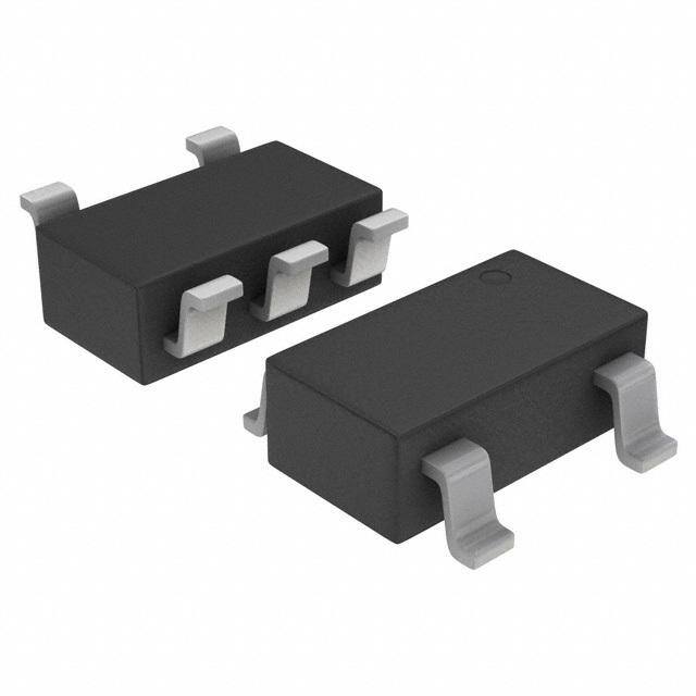
| 产品图片 |
|
| rohs | 符合RoHS无铅 / 符合限制有害物质指令(RoHS)规范要求 |
| 产品系列 | 电源管理 IC,低压差稳压器,ON Semiconductor NCP603SN330T1G- |
| 数据手册 | |
| 产品型号 | NCP603SN330T1G |
| 产品种类 | 低压差稳压器 |
| 供应商器件封装 | 5-TSOP |
| 其它名称 | NCP603SN330T1GOSCT |
| 包装 | 剪切带 (CT) |
| 商标 | ON Semiconductor |
| 回动电压—最大值 | 125 mV at 150 mA |
| 安装类型 | 表面贴装 |
| 安装风格 | SMD/SMT |
| 封装 | Reel |
| 封装/外壳 | 6-TSOP(0.059",1.50mm 宽)5 引线 |
| 封装/箱体 | TSOP-5 |
| 工作温度 | -40°C ~ 125°C |
| 工厂包装数量 | 3000 |
| 最大工作温度 | + 125 C |
| 最大输入电压 | 6 V |
| 最小工作温度 | - 40 C |
| 最小输入电压 | + 1.75 V |
| 标准包装 | 1 |
| 电压-跌落(典型值) | 0.157V @ 300mA |
| 电压-输入 | 最高 6V |
| 电压-输出 | 3.3V |
| 电压调节准确度 | 3 % |
| 电流-输出 | 300mA |
| 电流-限制(最小值) | 300mA |
| 稳压器拓扑 | 正,固定式 |
| 稳压器数 | 1 |
| 系列 | NCP603 |
| 线路调整率 | 10 mV |
| 负载调节 | 45 mV |
| 输出电压 | 3.3 V |
| 输出电流 | 300 mA |
| 输出端数量 | 1 Output |
| 输出类型 | Fixed |


- 商务部:美国ITC正式对集成电路等产品启动337调查
- 曝三星4nm工艺存在良率问题 高通将骁龙8 Gen1或转产台积电
- 太阳诱电将投资9.5亿元在常州建新厂生产MLCC 预计2023年完工
- 英特尔发布欧洲新工厂建设计划 深化IDM 2.0 战略
- 台积电先进制程称霸业界 有大客户加持明年业绩稳了
- 达到5530亿美元!SIA预计今年全球半导体销售额将创下新高
- 英特尔拟将自动驾驶子公司Mobileye上市 估值或超500亿美元
- 三星加码芯片和SET,合并消费电子和移动部门,撤换高东真等 CEO
- 三星电子宣布重大人事变动 还合并消费电子和移动部门
- 海关总署:前11个月进口集成电路产品价值2.52万亿元 增长14.8%


PDF Datasheet 数据手册内容提取
NCP603 300 mA High Performance CMOS LDO Regulator with Enable and Enhanced ESD Protection http://onsemi.com The NCP603 provides 300 mA of output current at fixed voltage options, or an adjustable output voltage from 5.0 V down to 1.250 V. It is designed for portable battery powered applications and offers high performance features such as low power operation, fast enable 5 1 response time, and low dropout. The device is designed to be used with low cost ceramic capacitors TSOP−5 SN SUFFIX and is packaged in the TSOP−5/SOT23−5. CASE 483 Features • Output Voltage Options: MARKING DIAGRAM Adjustable, 1.3 V, 1.5 V, 1.8 V, 2.5 V, 2.8 V, 3.0 V, 3.3 V, 3.5 V, 5.0 V • Adjustable Output by External Resistors from 5.0 V down to 1.250 V 5 • Fast Enable Turn−on Time of 15 (cid:2)s xxx AYW(cid:2) • (cid:2) Wide Supply Voltage Range Operating Range • 1 Excellent Line and Load Regulation • Typical Noise Voltage of 50 (cid:2)Vrms without a Bypass Capacitor xxx = Specific Device Code • Enhanced ESD Protection (HBM 3.5 kV, MM 200 V) A = Assembly Location • Y = Year These are Pb−Free Devices W = Work Week (cid:2) = Pb−Free Package Typical Applications • (Note: Microdot may be in either location) SMPS Post−Regulation • Hand−held Instrumentation & Audio Players • PIN CONNECTIONS Noise Sensitive Circuits – VCO, RF Stages, etc. • Camcorders and Cameras • Portable Computing Vin 1 5 Vout GND 2 VIN VOUT ENABLE 3 4 ADJ/NC* Fixed Voltage Only (Top View) Driver w/ + Current Limit - * ADJ − Adjustable Version + 1.25 V * NC − Fixed Voltage Version − GND Thermal Shutdown ORDERING INFORMATION ADJ Adjustable Version Only See detailed ordering and shipping information in the package dimensions section on page 12 of this data sheet. ENABLE Figure 1. Simplified Block Diagram © Semiconductor Components Industries, LLC, 201 1 Publication Order Number: January, 2013 − Rev. 3 NCP603/D
NCP603 PIN FUNCTION DESCRIPTION Pin No. Pin Name Description 1 Vin Positive Power Supply Input 2 GND Power Supply Ground; Device Substrate 3 ENABLE The Enable Input places the device into low−power standby when pulled to logic low (< 0.4 V). Connect to Vin if the function is not used. 4 ADJ/NC Output Voltage Adjust Input (Adjustable Version), No Connection (Fixed Voltage Versions) (Note 1) 5 Vout Regulated Output Voltage 1. True no connect. Printed circuit board traces are allowable. ABSOLUTE MAXIMUM RATINGS Rating Symbol Value Unit Input Voltage (Note 2) Vin −0.3 to 6.5 V Output, Enable, Adjustable Voltage Vout, ENABLE, ADJ −0.3 to 6.5 (or Vin + 0.3) V Whichever is Lower Maximum Junction Temperature TJ(max) 150 °C Storage Temperature TSTG −65 to 150 °C ESD Capability, Human Body Model (Note 3) ESDHBM 3500 V ESD Capability, Machine Model (Note 3) ESDMM 200 V Moisture Sensitivity Level MSL MSL1/260 − Stresses exceeding Maximum Ratings may damage the device. Maximum Ratings are stress ratings only. Functional operation above the Recommended Operating Conditions is not implied. Extended exposure to stresses above the Recommended Operating Conditions may affect device reliability. 2. Refer to ELECTRICAL CHARACTERISTICS and APPLICATION INFORMATION for Safe Operating Area. 3. This device series incorporates ESD protection and is tested by the following methods: ESD Human Body Model tested per AEC−Q100−002 (EIA/JESD22−A114) ESD Machine Model tested per AEC−Q100−003 (EIA/JESD22−A115) Latchup Current Maximum Rating: (cid:2)150 mA per JEDEC standard: JESD78. THERMAL CHARACTERISTICS Rating Symbol Value Unit Thermal Characteristics, TSOP−5 (Note 4) R(cid:3)JA °C/W Thermal Resistance, Junction−to−Air (Note 5) 215 4. Refer to ELECTRICAL CHARACTERISTICS and APPLICATION INFORMATION for Safe Operating Area. 5. Value based on copper area of 645 mm2 (or 1 in2) of 1 oz copper thickness. OPERATING RANGES (Note 6) Rating Symbol Min Max Unit Input Voltage (Note 7) Vin 1.75 6 V Adjustable Output Voltage (Adjustable Version Only) Vout 1.25 5.0 V Output Current Iout 0 300 mA Ambient Temperature TA −40 125 °C 6. Refer to ELECTRICAL CHARACTERISTICS and APPLICATION INFORMATION for Safe Operating Area. 7. Minimum Vin = 1.75 V or (Vout + VDO), whichever is higher. http://onsemi.com 2
NCP603 ELECTRICAL CHARACTERISTICS (Vin = 1.750 V, Vout = 1.250 V, Cin = Cout =1.0 (cid:2)F, for typical values TA = 25°C, for min/max values TA = −40°C to 125°C, unless otherwise specified.) (Note 8) Characteristic Symbol Test Conditions Min Typ Max Unit Regulator Output (Adjustable Voltage Version) Output Voltage Vout Iout = 1.0 mA to 150 mA 1.231 1.250 1.269 V Vin = 1.75 V to 6.0 V, (−1.5%) (+1.5%) Vout = ADJ Output Voltage Vout Iout = 1.0 mA to 300 mA 1.213 1.250 1.287 V (−3%) (+3%) Vin = 1.75 V to 6.0 V, Vout = ADJ = 1.25 V Power Supply Ripple Rejection (Note 9) PSRR Iout = 1.0 mA to 150 mA dB Vin = Vout + 1 V + 0.5 Vp−p − 62 − f = 120 Hz − 55 − f = 1.0 kHz − 38 − f = 10 kHz Line Regulation Regline Vin = 1.750 V to 6.0 V, − 1.0 10 mV Iout = 1.0 mA Load Regulation Regload Iout = 1.0 mA to 300 mA − 2.0 45 mV Output Noise Voltage (Note 9) Vn f = 10 Hz to 100 kHz − 50 − (cid:2)Vrms Output Short Circuit Current Isc 350 650 900 mA Dropout Voltage VDO Measured at: Vout – 2.0%, mV 1.25 V − 175 250 Iout = 150 mA, Figure 2 Dropout Voltage VDO Measured at: Vout – 2.0%, mV 1.25 V − 375 480 Iout = 300 mA, Figure 2 Output Current Limit (Note 9) Iout(max) 300 650 − mA Regulator Output (Fixed Voltage Version) (Vin = Vout + 0.5 V, Cin = Cout =1.0 (cid:2)F, for typical values TA = 25°C, for min/max values TA = −40°C to 125°C; unless otherwise noted.) (Note 8) Output Voltage Vout Iout = 1.0 mA to 150 mA (−2%) (+2%) V 1.3 V 1.270 1.3 1.326 1.5 V Vin = (Vout + 0.5 V) to 6.0 V 1.470 1.5 1.530 1.8 V 1.764 1.8 1.836 2.5 V 2.450 2.5 2.550 2.8 V 2.744 2.8 2.856 3.0 V 2.940 3.0 3.060 3.3 V 3.234 3.3 3.366 3.5 V 3.430 3.5 3.570 5.0 V 4.900 5.0 5.100 Output Voltage Vout Iout = 1.0 mA to 300 mA (−3%) (+3%) V 1.3 V 1.261 1.3 1.339 1.5 V Vin = (Vout + 0.5 V) to 6.0 V 1.455 1.5 1.545 1.8 V 1.746 1.8 1.854 2.5 V 2.425 2.5 2.575 2.8 V 2.716 2.8 2.884 3.0 V 2.910 3.0 3.090 3.3 V 3.201 3.3 3.399 3.5 V 3.395 3.5 3.605 5.0 V 4.850 5.0 5.150 Power Supply Ripple Rejection (Note 9) PSRR Iout = 1.0 mA to 150 mA dB Vin = Vout + 1 V + 0.5 Vp−p − 62 − f = 120 Hz − 55 − f = 1.0 kHz − 38 − f = 10 kHz Line Regulation Regline Vin = 1.750 V to 6.0 V, − 1.0 10 mV Iout = 1.0 mA Load Regulation Regload Iout = 1.0 mA to 150 mA − 2.0 30 mV − 2.0 45 Iout = 1.0 mA to 300 mA 8. Performance guaranteed over the indicated operating temperature range by design and/or characterization, production tested at TJ = TA = 25°C. Low duty cycle pulse techniques are used during testing to maintain the junction temperature as close to ambient as possible. 9. Values based on design and/or characterization. http://onsemi.com 3
NCP603 ELECTRICAL CHARACTERISTICS (Vin = 1.750 V, Vout = 1.250 V (adjustable version)), (Vin = Vout + 0.5 V (fixed version)), Cin = Cout =1.0 (cid:2)F, for typical values TA = 25°C, for min/max values TA = −40°C to 125°C, unless otherwise specified.) (Note 10) Characteristic Symbol Test Conditions Min Typ Max Unit Output Noise Voltage (Note 11) Vn f = 10 Hz to 100 kHz − 50 − (cid:2)Vrms Output Short Circuit Current Isc 350 650 900 mA Dropout Voltage VDO Measured at: Vout – 2.0% mV 1.3 V Iout = 150 mA − 175 250 1.5 V − 150 225 1.8 V − 125 175 2.5 V − 85 175 2.7 V to 5.0 V − 75 125 Dropout Voltage VDO Measured at: Vout – 2.0% mV 1.3 V − 375 480 Iout = 300 mA 1.5 V − 350 400 1.8 V − 245 340 2.5 V − 187 275 2.7 V to 5.0 V − 157 230 Output Current Limit (Note 11) Iout(max) 300 650 − mA General Disable Current IDIS ENABLE = 0 V, Vin = 6 V − 0.01 1.0 (cid:2)A −40°C ≤ TA ≤ 85°C Ground Current IGND ENABLE = 0.9 V, − 145 180 (cid:2)A Iout = 1.0 mA to 300 mA Thermal Shutdown Temperature (Note 11) TSD − 175 − °C Thermal Shutdown Hysteresis (Note 11) TSH − 10 − °C ADJ Input Bias Current IADJ −0.75 − 0.75 (cid:2)A Chip Enable ENABLE Input Threshold Voltage Vth(EN) V Voltage Increasing, Logic High 0.9 − − Voltage Decreasing, Logic Low − − 0.4 Enable Input Bias Current (Note 11) IEN − 3.0 100 nA Timing Output Turn On Time (Note 11) tEN ENABLE = 0 V to Vin (cid:2)s 1.25 V to 3.5 V − 15 25 5.0 V − 30 50 10.Performance guaranteed over the indicated operating temperature range by design and/or characterization, production tested at TJ = TA = 25°C. Low duty cycle pulse techniques are used during testing to maintain the junction temperature as close to ambient as possible. 11.Values based on design and/or characterization. http://onsemi.com 4
NCP603 VIN 1 5 VOUT CIN COUT 2 ENABLE 3 4 Figure 2. Typical Application Circuit for V = 1.250 V out (Adjustable Version) VIN 1 5 VOUT CIN COUT 2 R1 ENABLE 3 4 R2 Figure 3. Typical Application Circuit for Adjustable V out VIN 1 5 VOUT CIN COUT 2 3 4 Figure 4. Typical Application Circuit (Fixed Voltage Version) http://onsemi.com 5
NCP603 TYPICAL CHARACTERISTICS 1.260 1.260 GE (V)1.256 Iout = 1.0 mA GE (V)1.256 Iout = 1.0 mA A A T T L1.252 L1.252 O O V V T Iout = 150 mA T U U TP1.248 TP1.248 Iout = 150 mA U U O O V, out1.244 VVoinu t= = V AouDt J+ 0.5 V V, out1.244 VVoinu t= = 6 A.0D VJ 1.240 1.240 −40 −20 0 20 40 60 80 100 120 −40 −15 10 35 60 85 110 125 TA, TEMPERATURE (°C) TA, TEMPERATURE (°C) Figure 5. Output Voltage vs. Temperature Figure 6. Output Voltage vs. Temperature (V = V + 0.5 V) (V = 6.0 V) in out in 1.500 1.500 E (V)1.495 Iout = 1.0 mA E (V)1.495 Iout = 1.0 mA G G A A T T L1.490 L1.490 O O V V T T Iout = 150 mA PU1.485 Iout = 150 mA PU1.485 T T U U O O , ut1.480 , ut1.480 o o V V 1.475 1.475 −40 −15 10 35 60 85 110 125 −40 −15 10 35 60 85 110 125 TA, TEMPERATURE (°C) TA, TEMPERATURE (°C) Figure 7. Output Voltage vs. Temperature Figure 8. Output Voltage vs. Temperature (1.5 V Fixed Output, V = 2 V) (1.5 V Fixed Output, V = 6 V) in in 3.005 3.005 Iout = 1.0 mA 3.000 Iout = 1.0 mA V)3.000 V) E ( E ( G G2.995 TA2.995 Iout = 150 mA TA L L O O2.990 V V Iout = 150 mA T 2.990 T U U2.985 P P T T U2.985 U O O2.980 , ut , ut Vo2.980 Vo2.975 2.975 2.970 −40 −15 10 35 60 85 110 125 −40 −15 10 35 60 85 110 125 TA, TEMPERATURE (°C) TA, TEMPERATURE (°C) Figure 9. Output Voltage vs. Temperature Figure 10. Output Voltage vs. Temperature (3.0 V Fixed Output, V = 3.5 V) (3.0 V Fixed Output, V = 6 V) in in http://onsemi.com 6
NCP603 TYPICAL CHARACTERISTICS 5.000 5.000 Iout = 1.0 mA Iout = 1.0 mA V)4.995 V) 4.995 E ( E ( G4.990 G 4.990 TA Iout = 150 mA TA L L O4.985 O 4.985 V V T T Iout = 150 mA U4.980 U 4.980 P P T T U U O4.975 O 4.975 , ut , ut o o V4.970 V 4.970 4.965 4.965 −40 −15 10 35 60 85 110 125 −40 −15 10 35 60 85 110 125 TA, TEMPERATURE (°C) TA, TEMPERATURE (°C) Figure 11. Output Voltage vs. Temperature Figure 12. Output Voltage vs. Temperature (5.0 V Fixed Output, V = 5.5 V) (5.0 V Fixed Output, V = 6 V) in in 250 250 AGE (mV) 200 Vout = ADJ Iout = 150 mA GE (mV) 200 Iout = 150 mA Vout = 11..2550 VV T A OL 150 LT 150 1.80 V V O OUT UT V 2.80 V P 100 O 100 O P R Iout = 50 mA O D R 3.00 V , DO 50 , DO 50 5.00 V V D V 0 Iout = 1.0 mA 0 −40 −20 0 20 40 60 80 100 120 −40 −20 0 20 40 60 80 100 120 TA, TEMPERATURE (°C) TA, TEMPERATURE (°C) Figure 13. Dropout Voltage vs. Temperature Figure 14. Dropout Voltage vs. Temperature (Over Current Range) (Over Output Voltage) 6.0 800 5.5 Iout = 0 mA 5.0 V V) 5.0 Cout = 1.0 (cid:2)F V) AGE ( 44..50 TEAN =A B2L5E°C = Vin LD (m750 T O Enable Increasing OL 3.5 3.0 V 3.3 V H V S T 3.0 RE700 PU 2.5 2.80 V TH Enable Decreasing UT 2.0 1.5 V 1.80 V E O BL V, out 11..50 1.25 V ENA650 Vin = 5.5 V 0.5 0 600 0 1.0 2.0 3.0 4.0 5.0 6.0 −40 −15 10 35 60 85 110 125 Vin, INPUT VOLTAGE (V) TA, TEMPERATURE (°C) Figure 15. Output Voltage vs. Input Voltage Figure 16. Enable Threshold vs. Temperature http://onsemi.com 7
NCP603 TYPICAL CHARACTERISTICS 6.0 154 Iout = 1.0 mA (cid:2)T (A) 5.0 (cid:2)T (A) 146 Vout = 5.0 V Iout = 150 mA N N 138 E 4.0 E R R R R 130 U U C 3.0 C E D 122 L N AB 2.0 OU 114 Vout = 1.25 V Iout = 1.0 mA S R DI ENABLE = 0 V G , DIS 1.0 , ND 106 Iout = 150 mA I G 98 I ENABLE = 0.9 V 0 90 −40 −15 10 35 60 85 110 125 −40 −20 0 20 40 60 80 100 120 TA, TEMPERATURE (°C) TA, TEMPERATURE (°C) Figure 17. Ground Current (Sleep Mode) vs. Figure 18. Ground Current (Run Mode) vs. Temperature Temperature 160 106 3.0 V A) 140 2.8 V A) 105 (cid:2)NT ( 120 1.5 V 3.3 V 5.0 V (cid:2)NT ( 104 E 1.8 V 1.25 V E R R R 100 R 103 U U C C D 80 D 102 N N OU 60 OU 101 R R , GD 40 , GD 100 GN 20 GN 99 Vout = ADJ I I Vin = 1.75 V 0 98 0 1.0 2.0 3.0 4.0 5.0 6.0 0 25 50 75 100 125 150 Vin, INPUT VOLTAGE (V) Iout, OUTPUT CURRENT (mA) Figure 19. Ground Current vs. Input Voltage Figure 20. Ground Current vs. Output Current 400 A) n T ( N E R300 R U C S A BI200 T U P N J I100 D A , J D A I 0 −40 −20 0 20 40 60 80 100 120 TA, TEMPERATURE (°C) Figure 21. ADJ Input Bias Current vs. Temperature http://onsemi.com 8
NCP603 TYPICAL CHARACTERISTICS A) 650 700 m T ( A) 600 N m RE 600 T ( UR MI 500 C LI T T 400 CUI 550 REN R R 300 CI U T C OR 500 , ax) 200 H m T S out( 100 U I P T 450 0 OU −40 −20 0 20 40 60 80 100 120 0 1.0 2.0 3.0 4.0 5.0 6.0 , SC TA, TEMPERATURE (°C) Vin, INPUT VOLTAGE (V) I Figure 22. Output Short Circuit Current vs. Figure 23. Current Limit vs. Input Voltage Temperature 4.0 5.0 V) mV) m N ( 3.0 ON ( 4.0 O TI ATI LA UL 3.0 U G G 2.0 E E R NE R OAD 2.0 LI L eg, line 1.0 Vin = (Vout + 0.5 V) to 6.0 V g, load 1.0 R Iout = 1.0 mA Re Iout = 1.0 mA to 150 mA 0 0 −40 −20 0 20 40 60 80 100 120 −40 −15 10 35 60 85 110 125 TA, TEMPERATURE (°C) TA, TEMPERATURE (°C) Figure 24. Line Regulation vs. Temperature Figure 25. Load Regulation vs. Temperature 45 80 (cid:2)s) 40 70 1.25 V E ( M 60 N TI 35 5.0 V 3.3 V N O 30 dB) 50 UR R ( 40 5.0 V T 25 R UT 3.0 V PS 30 P UT 20 1.5 V 20 Vin = Vout + 1.0 V O Vripple = 0.5 Vp−p , N 15 1.25 V (ADJ) 10 Cout = 1.0 (cid:2)F tE Iout = 1.0 mA to 150 mA 10 0 −40 −20 0 20 40 60 80 100 120 0.1 1.0 10 100 TA, TEMPERATURE (°C) f, FREQUENCY (kHz) Figure 26. Output Turn On Time vs. Figure 27. Power Supply Ripple Rejection vs. Temperature Frequency http://onsemi.com 9
NCP603 TYPICAL CHARACTERISTICS 10 Unstable Region (cid:4)) Vout = 5.0 V R ( S R E 1.0 Vout = 1.25 V O T CI A Stable Region P A C T 0.1 U P UT Cout = 1.0 (cid:2)F to 10 (cid:2)F O TA = −40°C to 125°C Vin = up to 6.0 V 0.01 0 25 50 75 100 125 150 Iout, OUTPUT CURRENT (mA) Figure 28. Output Stability with Output Capacitor ESR over Output Current Vout = 1.25 V Figure 29. Load Transient Response (1.0 (cid:2)F) Vout = 1.25 V Figure 30. Load Transient Response (10 (cid:2)F) http://onsemi.com 10
NCP603 DEFINITIONS Load Regulation Line Regulation The change in output voltage for a change in output load The change in output voltage for a change in input voltage. current at a constant temperature. The measurement is made under conditions of low dissipation or by using pulse techniques such that the Dropout Voltage average junction temperature is not significantly affected. The input/output differential at which the regulator output no longer maintains regulation against further reductions in Line Transient Response input voltage. Measured when the output drops 2% below its Typical output voltage overshoot and undershoot nominal. The junction temperature, load current, and response when the input voltage is excited with a given minimum input supply requirements affect the dropout level. slope. Output Noise Voltage Load Transient Response This is the integrated value of the output noise over a Typical output voltage overshoot and undershoot specified frequency range. Input voltage and output load response when the output current is excited with a given current are kept constant during the measurement. Results slope between no−load and full−load conditions. are expressed in (cid:2)V or nV √ Hz. rms Thermal Protection Ground Current Internal thermal shutdown circuitry is provided to protect Ground Current is the current that flows through the the integrated circuit in the event that the maximum junction ground pin when the regulator operates without a load on its temperature is exceeded. When activated at typically 175°C, output (I ). This consists of internal IC operation, bias, the regulator turns off. This feature is provided to prevent GND etc. It is actually the difference between the input current failures from accidental overheating. (measured through the LDO input pin) and the output load Maximum Package Power Dissipation current. If the regulator has an input pin that reduces its The power dissipation level at which the junction internal bias and shuts off the output (enable/disable temperature reaches its maximum operating value. function), this term is called the standby current (I .) STBY APPLICATIONS INFORMATION The NCP603 series regulator is self−protected with output, there is no resistor divider. If the part is enabled internal thermal shutdown and internal current limit. Typical under no−load conditions, leakage current through the pass application circuits are shown in Figures 2 and 3. transistor at junction temperatures above 85°C can approach several microamperes, especially as junction temperature Input Decoupling (Cin) approaches 150°C. If this leakage current is not directed into A ceramic or tantalum 1.0 (cid:2)F capacitor is recommended a load, the output voltage will rise up to a level and should be connected close to the NCP603 package. approximately 20 mV above nominal. Higher capacitance and lower ESR will improve the overall The NCP603 contains an overshoot clamp circuit to line transient response. improve transient response during a load current step release. When output voltage exceeds the nominal by Output Decoupling (C ) out approximately 20 mV, this circuit becomes active and The NCP603 is a stable component and does not require clamps the output from further voltage increase. Tying the a minimum Equivalent Series Resistance (ESR) for the ENABLE pin to V will ensure that the part is active output capacitor. The minimum output decoupling value is in 1.0 (cid:2)F and can be augmented to fulfill stringent load whenever the supply voltage is present, thus guaranteeing that the clamp circuit is active whenever leakage current is transient requirements. The regulator works with ceramic present. chip capacitors as well as tantalum devices. Larger values When the NCP603 adjustable regulator is disabled, the improve noise rejection and load regulation transient overshoot clamp circuit becomes inactive and the pass response. Figure 28 shows the stability region for a range of transistor leakage will charge any capacitance on V . If no operating conditions and ESR values. out load is present, the output can charge up to within a few No−Load Regulation Considerations millivolts of Vin. In most applications, the load will present The NCP603 adjustable regulator will operate properly some impedance to V such that the output voltage will be out under conditions where the only load current is through the inherently clamped at a safe level. A minimum load of resistor divider that sets the output voltage. However, in the 10(cid:2)A is recommended. case where the NCP603 is configured to provide a 1.250 V http://onsemi.com 11
NCP603 Noise Decoupling Thermal The NCP603 is a low noise regulator and needs no As power in the NCP603 increases, it might become external noise reduction capacitor. Unlike other low noise necessary to provide some thermal relief. The maximum regulators which require an external capacitor and have slow power dissipation supported by the device is dependent startup times, the NCP603 operates without a noise upon board design and layout. Mounting pad configuration reduction capacitor, has a typical 15 (cid:2)s start up delay and on the PCB, the board material, and the ambient temperature achieves a 50 (cid:2)V overall noise level between 10 Hz and affect the rate of junction temperature rise for the part. When rms 100 kHz. the NCP603 has good thermal conductivity through the PCB, the junction temperature will be relatively low with Enable Operation high power applications. The maximum dissipation the The enable pin will turn the regulator on or off. The NCP603 can handle is given by: threshold limits are covered in the electrical characteristics table in this data sheet. The turn−on/turn−off transient PD(MAX)(cid:3)TJ(MAX)(cid:9)TA voltage being supplied to the enable pin should exceed a R(cid:3)JA (eq. 3) slew rate of 10 mV/(cid:2)s to ensure correct operation. If the Since TJ is not recommended to exceed 125(cid:3)C (TJ(MAX)), then the NCP603 can dissipate up to 465 mW when the enable function is not to be used then the pin should be connected to Vin. ambient temperature (TA) is 25(cid:3)C and the device is assembled on 1 oz PCB with 645 mm2 area. Output Voltage Adjust The power dissipated by the NCP603 can be calculated The output voltage can be adjusted from 1 times from the following equations: (Figure2) to 4 times (Figure 3) the typical 1.250 V PD(cid:12)VIN(IGND@IOUT)(cid:5)IOUT(VIN(cid:9)VOUT) regulation voltage via the use of resistors between the output (eq. 4) and the ADJ input. The output voltage and resistors are or chosen using Equation 1 and Equation 2. (cid:4) (cid:6) PD(MAX)(cid:5)(VOUT(cid:7)IOUT) VOUT(cid:3)1.250 1(cid:5)RR12 (cid:5)(IADJ(cid:7)R1) (eq. 1) VIN(MAX)(cid:12) IOUT(cid:5)IGND (eq. 5) (cid:8) (cid:10) (cid:8) (cid:10) R1(cid:3)R2* [Vout(cid:9)(IADJ*R1)](cid:9)1 (cid:11)R2 Vout(cid:9)1 1.25 1.25 Hints (eq. 2) Vin and GND printed circuit board traces should be as wide as possible. When the impedance of these traces is Input bias current I is typically less than 150 nA. ADJ high, there is a chance to pick up noise or cause the regulator Choose R2 arbitrarily t minimize errors due to the bias to malfunction. Place external components, especially the current and to minimize noise contribution to the output output capacitor, as close as possible to the NCP603, and voltage. Use Equation 2 to find the required value for R1. make traces as short as possible. DEVICE ORDERING INFORMATION Device Marking Code Version Package Shipping* NCP603SNADJT1G AAU ADJ NCP603SN130T1G AAF 1.3 V NCP603SN150T1G AAV 1.5 V NCP603SN180T1G AAW 1.8 V NCP603SN250T1G ACL 2.5 V TSOP−5 3000/Tape & Reel NCP603SN280T1G AAX 2.8 V (Pb−Free) NCP603SN300T1G AAY 3.0 V NCP603SN330T1G AAZ 3.3 V NCP603SN350T1G AA2 3.5 V NCP603SN500T1G AA3 5.0 V *For additional information on our Pb−Free strategy and soldering details, please download the ON Semiconductor Soldering and Mounting Techniques Reference Manual, SOLDERRM/D. http://onsemi.com 12
NCP603 PACKAGE DIMENSIONS TSOP−5 CASE 483−02 ISSUE H NOTES: 1. DIMENSIONING AND TOLERANCING PER NOTE 5 D5X ASME Y14.5M, 1994. 2. CONTROLLING DIMENSION: MILLIMETERS. 0.20 C A B 3. MAXIMUM LEAD THICKNESS INCLUDES 2X 0.10 T LEAD FINISH THICKNESS. MINIMUM LEAD THICKNESS IS THE MINIMUM THICKNESS M OF BASE MATERIAL. 2X 0.20 T 5 4 B S 4. DMIOMLEDN FSLIOANSSH ,A P ARNODT RBU DSOIO NNOST, OINRC GLUATDEE 1 2 3 BURRS. K 5. OPTIONAL CONSTRUCTION: AN L DETAIL Z ADDITIONAL TRIMMED LEAD IS ALLOWED G IN THIS LOCATION. TRIMMED LEAD NOT TO EXTEND MORE THAN 0.2 FROM BODY. A MILLIMETERS DIM MIN MAX DETAIL Z A 3.00 BSC J B 1.50 BSC C C 0.90 1.10 0.05 H SPELAATNIENG GD 0.02.595 BS0C.50 H 0.01 0.10 T J 0.10 0.26 K 0.20 0.60 SOLDERING FOOTPRINT* ML 1.02 5(cid:3) 110.5 (cid:3) 5 S 2.50 3.00 1.9 0.074 0.95 0.037 2.4 0.094 1.0 0.039 0.7 (cid:4) (cid:6) 0.028 SCALE 10:1 mm inches *For additional information on our Pb−Free strategy and soldering details, please download the ON Semiconductor Soldering and Mounting Techniques Reference Manual, SOLDERRM/D. ON Semiconductor and are registered trademarks of Semiconductor Components Industries, LLC (SCILLC). SCILLC owns the rights to a number of patents, trademarks, copyrights, trade secrets, and other intellectual property. A listing of SCILLC’s product/patent coverage may be accessed at www.onsemi.com/site/pdf/Patent−Marking.pdf. SCILLC reserves the right to make changes without further notice to any products herein. SCILLC makes no warranty, representation or guarantee regarding the suitability of its products for any particular purpose, nor does SCILLC assume any liability arising out of the application or use of any product or circuit, and specifically disclaims any and all liability, including without limitation special, consequential or incidental damages. “Typical” parameters which may be provided in SCILLC data sheets and/or specifications can and do vary in different applications and actual performance may vary over time. All operating parameters, including “Typicals” must be validated for each customer application by customer’s technical experts. SCILLC does not convey any license under its patent rights nor the rights of others. SCILLC products are not designed, intended, or authorized for use as components in systems intended for surgical implant into the body, or other applications intended to support or sustain life, or for any other application in which the failure of the SCILLC product could create a situation where personal injury or death may occur. Should Buyer purchase or use SCILLC products for any such unintended or unauthorized application, Buyer shall indemnify and hold SCILLC and its officers, employees, subsidiaries, affiliates, and distributors harmless against all claims, costs, damages, and expenses, and reasonable attorney fees arising out of, directly or indirectly, any claim of personal injury or death associated with such unintended or unauthorized use, even if such claim alleges that SCILLC was negligent regarding the design or manufacture of the part. SCILLC is an Equal Opportunity/Affirmative Action Employer. This literature is subject to all applicable copyright laws and is not for resale in any manner. PUBLICATION ORDERING INFORMATION LITERATURE FULFILLMENT: N. American Technical Support: 800−282−9855 Toll Free ON Semiconductor Website: www.onsemi.com Literature Distribution Center for ON Semiconductor USA/Canada P.O. Box 5163, Denver, Colorado 80217 USA Europe, Middle East and Africa Technical Support: Order Literature: http://www.onsemi.com/orderlit Phone: 303−675−2175 or 800−344−3860 Toll Free USA/Canada Phone: 421 33 790 2910 Fax: 303−675−2176 or 800−344−3867 Toll Free USA/Canada Japan Customer Focus Center For additional information, please contact your local Email: orderlit@onsemi.com Phone: 81−3−5817−1050 Sales Representative http://onsemi.com NCP603/D 13