ICGOO在线商城 > 隔离器 > 光隔离器 - 晶体管,光电输出 > TLP183(GRL-TPL,E
 Datasheet下载
- 型号: TLP183(GRL-TPL,E
- 制造商: Toshiba America Electronic Components, Inc.
- 库位|库存: xxxx|xxxx
- 要求:
| 数量阶梯 | 香港交货 | 国内含税 |
| +xxxx | $xxxx | ¥xxxx |
查看当月历史价格
查看今年历史价格
TLP183(GRL-TPL,E产品简介:
ICGOO电子元器件商城为您提供TLP183(GRL-TPL,E由Toshiba America Electronic Components, Inc.设计生产,在icgoo商城现货销售,并且可以通过原厂、代理商等渠道进行代购。 TLP183(GRL-TPL,E价格参考。Toshiba America Electronic Components, Inc.TLP183(GRL-TPL,E封装/规格:光隔离器 - 晶体管,光电输出, 光隔离器 晶体管 输出 3750Vrms 1 通道 6-SO,4 个接脚。您可以下载TLP183(GRL-TPL,E参考资料、Datasheet数据手册功能说明书,资料中有TLP183(GRL-TPL,E 详细功能的应用电路图电压和使用方法及教程。
Toshiba Semiconductor and Storage的TLP183(GRL-TPL,E) 是一款光隔离器,采用晶体管光电输出设计。这款器件主要用于需要电气隔离的应用场景,特别是在高噪声环境或存在高电压差的地方。以下是其主要应用场景:

 1. 工业自动化与控制
   在工业环境中,TLP183可以用于将控制系统与传感器、执行器等外部设备进行电气隔离。例如,在PLC(可编程逻辑控制器)中,它可以防止外部干扰信号影响控制系统,确保数据传输的稳定性和可靠性。

 2. 电力系统
   TLP183适用于电力系统的监控和保护电路中。例如,在智能电表、断路器和继电器控制电路中,它可以通过光耦合实现输入和输出之间的电气隔离,避免高压侧对低压控制电路的影响,提高系统的安全性。

 3. 通信设备
   在通信设备中,TLP183可以用于隔离不同的电源域或信号路径,防止信号串扰和电磁干扰(EMI)。例如,在光纤通信模块中,它可以隔离高速信号和低速控制信号,确保通信的稳定性和抗干扰能力。

 4. 医疗设备
   医疗设备通常需要严格的安全标准,特别是涉及到患者接触的部分。TLP183可以用于隔离患者与设备之间的电气连接,防止漏电流对患者造成伤害。例如,在心电图仪、监护仪等设备中,它可以提供可靠的电气隔离,确保设备的安全性。

 5. 汽车电子
   在汽车电子系统中,TLP183可以用于隔离不同电压级别的电路,如电池管理系统(BMS)中的电池监测电路与控制单元之间的隔离。此外,它还可以用于车载网络通信中的信号隔离,确保各模块之间的电气独立性,提高系统的可靠性和安全性。

 6. 家用电器
   在一些高端家用电器中,TLP183可以用于隔离主控板与外部接口之间的信号,防止外部干扰影响内部电路。例如,在智能家电中,它可以隔离Wi-Fi模块与主控芯片之间的信号,确保通信的稳定性。

总之,TLP183(GRL-TPL,E) 光隔离器凭借其高可靠性和电气隔离特性,广泛应用于各种需要防止电气干扰、确保安全性和可靠性的场合。
| 参数 | 数值 |
| 产品目录 | |
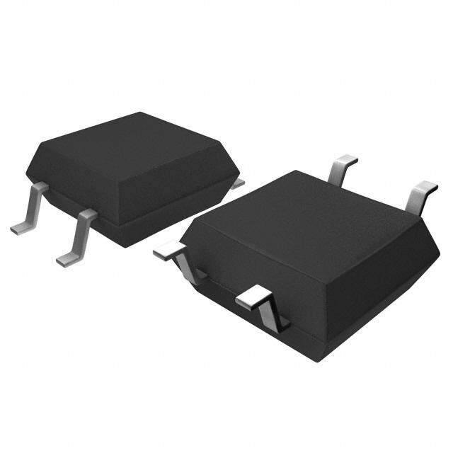
| 描述 | OPTOISO 3.75KV TRANS 6-SO 4 LEAD |
| 产品分类 | |
| 品牌 | Toshiba Semiconductor and Storage |
| 数据手册 | http://www.semicon.toshiba.co.jp/info/docget.jsp?type=datasheet&lang=en&pid=TLP183 |
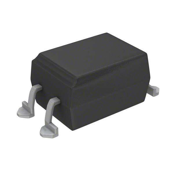
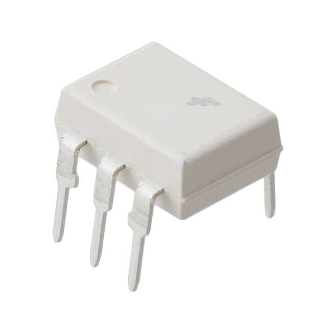
| 产品图片 |
|
| 产品型号 | TLP183(GRL-TPL,E |
| rohs | 无铅 / 符合限制有害物质指令(RoHS)规范要求 |
| 产品系列 | - |
| Vce饱和值(最大值) | 300mV |
| 上升/下降时间(典型值) | 2µs, 3µs |
| 供应商器件封装 | 6-SO, 4 个接脚 |
| 其它名称 | TLP183(GRL-TPL,E(T |
| 包装 | 带卷 (TR) |
| 安装类型 | 表面贴装 |
| 封装/外壳 | 6-SMD(4 个接脚),鸥形翼 |
| 工作温度 | -55°C ~ 125°C |
| 打开/关闭时间(典型值) | 3µs, 3µs |
| 标准包装 | 3,000 |
| 特色产品 | http://www.digikey.cn/product-highlights/zh/low-current-input-transistor-optocoupler-series/52115 |
| 电压-正向(Vf)(典型值) | 1.25V |
| 电压-输出(最大值) | 80V |
| 电压-隔离 | 3750Vrms |
| 电流-DC正向(If) | 50mA |
| 电流-输出/通道 | 50mA |
| 电流传输比(最大值) | 200% @ 500µA |
| 电流传输比(最小值) | 100% @ 500µA |
| 输入类型 | DC |
| 输出类型 | 晶体管 |
| 通道数 | 1 |


(B)(TU)-VG.jpg)


- 商务部:美国ITC正式对集成电路等产品启动337调查
- 曝三星4nm工艺存在良率问题 高通将骁龙8 Gen1或转产台积电
- 太阳诱电将投资9.5亿元在常州建新厂生产MLCC 预计2023年完工
- 英特尔发布欧洲新工厂建设计划 深化IDM 2.0 战略
- 台积电先进制程称霸业界 有大客户加持明年业绩稳了
- 达到5530亿美元!SIA预计今年全球半导体销售额将创下新高
- 英特尔拟将自动驾驶子公司Mobileye上市 估值或超500亿美元
- 三星加码芯片和SET,合并消费电子和移动部门,撤换高东真等 CEO
- 三星电子宣布重大人事变动 还合并消费电子和移动部门
- 海关总署:前11个月进口集成电路产品价值2.52万亿元 增长14.8%
.jpg)

PDF Datasheet 数据手册内容提取
TLP183 Photocouplers Infrared LED & Photo Transistor TTTTLLLLPPPP111188883333 1111.... AAAApppppppplllliiiiccccaaaattttiiiioooonnnnssss • Office Equipment • Programmable Logic Controllers (PLCs) • AC Adapters • I/O Interface Boards 2222.... GGGGeeeennnneeeerrrraaaallll TLP183 is a low input type phototransistor coupler that consists of a photo transistor optically coupled to an infrared LED in a SO6 package. TLP183 is guaranteed high isolation voltage (3750 Vrms) and wide operating temperature (T = -55 to 125 ). a TLP183 is smaller than DIP package, it's suitable for high density surface mounting applications such as programmable controllers. 3333.... FFFFeeeeaaaattttuuuurrrreeeessss (1) Collector-emitter voltage: 80 V (min) (2) Current transfer ratio: 50 % (min) (@I = 0.5 mA, V = 5 V) F CE GB Rank: 100 % (min) (@I = 0.5 mA, V = 5 V) F CE (3) Isolation voltage: 3750 Vrms (min) (4) Operating temperature: -55 to 125 (5) Safety standards UL-recognized: UL 1577, File No.E67349 cUL-recognized: CSA Component Acceptance Service No.5A File No.E67349 VDE-approved: EN 60747-5-5, EN 62368-1 ((((NNNNooootttteeee 1111)))) CQC-approved: GB4943.1, GB8898 Thailand Factory Note 1:When a VDE approved type is needed, please designate the OOOOppppttttiiiioooonnnn ((((VVVV4444)))). 4444.... PPPPaaaacccckkkkaaaaggggiiiinnnngggg aaaannnndddd PPPPiiiinnnn AAAAssssssssiiiiggggnnnnmmmmeeeennnntttt 1: Anode 3: Cathode 4: Emitter 6: Collector 11-4M1S Start of commercial production 2013-09 ©2016-2019 1 2019-11-18 Toshiba Electronic Devices & Storage Corporation Rev.7.0
TLP183 5555.... MMMMeeeecccchhhhaaaannnniiiiccccaaaallll PPPPaaaarrrraaaammmmeeeetttteeeerrrrssss Characteristics Min Unit Creepage distances 5.0 mm Clearance 5.0 Internal isolation thickness 0.4 6666.... AAAAbbbbssssoooolllluuuutttteeee MMMMaaaaxxxxiiiimmmmuuuummmm RRRRaaaattttiiiinnnnggggssss ((((NNNNooootttteeee)))) ((((UUUUnnnnlllleeeessssssss ooootttthhhheeeerrrrwwwwiiiisssseeee ssssppppeeeecccciiiiffffiiiieeeedddd,,,, TTTTaaaa ==== 22225555 )))) Characteristics Symbol Note Rating Unit LED Input forward current I 50 mA F Input forward current (pulsed) I (Note 1) 1 A FP Input forward current derating (T ≥ 90 ) ∆I /∆T -1.11 mA/ a F a Input reverse voltage V 5 V R Input power dissipation P 100 mW D Input power dissipation (T ≥ 90 ) ∆P /∆T -2.22 mW/ a D a derating Junction temperature T 135 j Detector Collector-emitter voltage V 80 V CEO Emitter-collector voltage V 7 V ECO Collector current I 50 mA C Collector power dissipation P 150 mW C Collector power dissipation (T ≥ 25 ) ∆P /∆T -1.36 mW/ a C a derating Junction temperature T 135 j Common Operating temperature T -55 to 125 opr Storage temperature T -55 to 125 stg Lead soldering temperature (10 s) T 260 sol Total power dissipation P 200 mW T Total power dissipation (T ≥ 25 ) ∆P /∆T -1.82 mW/ a T a derating Isolation voltage AC, 60 s, R.H. ≤ 60 % BV (Note 2) 3750 Vrms S Note: Using continuously under heavy loads (e.g. the application of high temperature/current/voltage and the significant change in temperature, etc.) may cause this product to decrease in the reliability significantly even if the operating conditions (i.e. operating temperature/current/voltage, etc.) are within the absolute maximum ratings. Please design the appropriate reliability upon reviewing the Toshiba Semiconductor Reliability Handbook ("Handling Precautions"/"Derating Concept and Methods") and individual reliability data (i.e. reliability test report and estimated failure rate, etc). Note 1:Pulse width (PW) ≤ 0.1 ms, f = 100 Hz Note 2:This device is considered as a two-terminal device: Pins 1 and 3 are shorted together, and pins 4 and 6 are shorted together. ©2016-2019 2 2019-11-18 Toshiba Electronic Devices & Storage Corporation Rev.7.0
TLP183 7777.... EEEElllleeeeccccttttrrrriiiiccccaaaallll CCCChhhhaaaarrrraaaacccctttteeeerrrriiiissssttttiiiiccccssss ((((UUUUnnnnlllleeeessssssss ooootttthhhheeeerrrrwwwwiiiisssseeee ssssppppeeeecccciiiiffffiiiieeeedddd,,,, TTTTaaaa ==== 22225555 )))) Characteristics Symbol Note Test Condition Min Typ. Max Unit LED Input forward voltage V I = 10 mA 1.1 1.25 1.4 V F F Input reverse current I V = 5 V 5 µA R R Input capacitance C V = 0 V, f = 1 MHz 30 pF t Detector Collector-emitter breakdown V I = 0.5 mA 80 V (BR)CEO C voltage Emitter-collector breakdown V I = 0.1 mA 7 V (BR)ECO E voltage Dark Current I V = 48 V 0.01 0.08 µA DARK CE V = 48 V, T = 85 2 50 CE a Collector-emitter capacitance C V = 0 V, f = 1 MHz 10 pF CE 8888.... CCCCoooouuuupppplllleeeedddd EEEElllleeeeccccttttrrrriiiiccccaaaallll CCCChhhhaaaarrrraaaacccctttteeeerrrriiiissssttttiiiiccccssss ((((UUUUnnnnlllleeeessssssss ooootttthhhheeeerrrrwwwwiiiisssseeee ssssppppeeeecccciiiiffffiiiieeeedddd,,,, TTTTaaaa ==== 22225555 )))) Characteristics Symbol Note Test Condition Min Typ. Max Unit Current transfer ratio I /I (Note 1) I = 5 mA, V = 5 V 50 600 % C F F CE I = 5 mA, V = 5 V, GB Rank 100 600 F CE I = 0.5 mA, V = 5 V 50 600 F CE I = 0.5 mA, V = 5 V, GB Rank 100 600 F CE Saturated current transfer ratio I /I I = 1 mA, V = 0.4 V 60 C F(sat) F CE I = 1 mA, V = 0.4 V, GB Rank 30 F CE Collector-emitter saturation voltage V I = 2.4 mA, I = 8 mA 0.3 V CE(sat) C F I = 0.2 mA, I = 1 mA 0.2 C F I = 0.2 mA, I = 1 mA, GB Rank 0.3 C F OFF-state collector current I V = 0.7 V, V = 48 V 10 µA C(off) F CE Note 1:See Table 8.1 for current transfer ratio. TTTTaaaabbbblllleeee 8888....1111 CCCCuuuurrrrrrrreeeennnntttt TTTTrrrraaaannnnssssffffeeeerrrr RRRRaaaattttiiiioooo ((((CCCCTTTTRRRR)))) RRRRaaaannnnkkkk ((((NNNNooootttteeee)))) ((((UUUUnnnnlllleeeessssssss ooootttthhhheeeerrrrwwwwiiiisssseeee ssssppppeeeecccciiiiffffiiiieeeedddd,,,, TTTTaaaa ==== 22225555 )))) Rank Current transfer ratio Current transfer ratio Marking of Rank short Note Test Condition I /I I /I Unit C F C F classification code (min) (max) Blank I = 5 mA, V = 5 V 50 600 Blank, YE, GR, GB, % F CE BL, Y+, G, G+, B I = 0.5 mA, V = 5 V F CE Y I = 5 mA, V = 5 V 50 150 YE F CE I = 0.5 mA, V = 5 V F CE GR I = 5 mA, V = 5 V 100 300 GR F CE I = 0.5 mA, V = 5 V F CE GB I = 5 mA, V = 5 V 100 600 GB, GR, BL F CE I = 0.5 mA, V = 5 V F CE BL I = 5 mA, V = 5 V 200 600 BL F CE I = 0.5 mA, V = 5 V F CE YH I = 0.5 mA, V = 5 V 75 150 Y+ F CE GRL GL (Note 1) I = 0.5 mA, V = 5 V 100 200 G F CE GRH GH (Note 1) I = 0.5 mA, V = 5 V 150 300 G+ F CE BLL B (Note 1) I = 0.5 mA, V = 5 V 200 400 B F CE Note: Specify both the part number and a rank in this format when ordering. Example: TLP183(GB,E For safety standard certification, however, specify the part number alone. Example: TLP183(GB,E → TLP183 Note 1:A rank in the order name is sometimes omitted like above "Rank short code". ©2016-2019 3 2019-11-18 Toshiba Electronic Devices & Storage Corporation Rev.7.0
TLP183 9999.... IIIIssssoooollllaaaattttiiiioooonnnn CCCChhhhaaaarrrraaaacccctttteeeerrrriiiissssttttiiiiccccssss ((((UUUUnnnnlllleeeessssssss ooootttthhhheeeerrrrwwwwiiiisssseeee ssssppppeeeecccciiiiffffiiiieeeedddd,,,, TTTTaaaa ==== 22225555 )))) Characteristics Symbol Note Test Condition Min Typ. Max Unit Total capacitance (input to output) C (Note 1) V = 0 V, f = 1 MHz 0.8 pF S S Isolation resistance RS (Note 1) VS = 500 V, R.H. ≤ 60 % 1012 1014 Ω Isolation voltage BV (Note 1) AC, 60 s 3750 Vrms S Note 1:This device is considered as a two-terminal device: Pins 1 and 3 are shorted together, and pins 4 and 6 are shorted together. 11110000.... SSSSwwwwiiiittttcccchhhhiiiinnnngggg CCCChhhhaaaarrrraaaacccctttteeeerrrriiiissssttttiiiiccccssss ((((UUUUnnnnlllleeeessssssss ooootttthhhheeeerrrrwwwwiiiisssseeee ssssppppeeeecccciiiiffffiiiieeeedddd,,,, TTTTaaaa ==== 22225555 )))) Characteristics Symbol Note Test Condition Min Typ. Max Unit Rise time t V = 10 V, I = 2 mA, 2 µs r CC C R = 100 Ω Fall time t L 3 f Turn-on time t 3 on Turn-off time t 3 off Turn-on time t See Fig. 10.1 1.3 on R = 1.9 kΩ, V = 5 V, Storage time t L CC 20 s I = 16 mA F Turn-off time t 35 off Turn-on time t See Fig. 10.1 10 on R = 4.7 kΩ, V = 5 V, Storage time t L CC 9 s I = 1.6 mA F Turn-off time t 47 off FFFFiiiigggg.... 11110000....1111 SSSSwwwwiiiittttcccchhhhiiiinnnngggg TTTTiiiimmmmeeee TTTTeeeesssstttt CCCCiiiirrrrccccuuuuiiiitttt aaaannnndddd WWWWaaaavvvveeeeffffoooorrrrmmmm ©2016-2019 4 2019-11-18 Toshiba Electronic Devices & Storage Corporation Rev.7.0
TLP183 11111111.... CCCChhhhaaaarrrraaaacccctttteeeerrrriiiissssttttiiiiccccssss CCCCuuuurrrrvvvveeeessss ((((NNNNooootttteeee)))) FFFFiiiigggg.... 11111111....1111 IIIIFFFF ---- TTTTaaaa FFFFiiiigggg.... 11111111....2222 PPPPCCCC ---- TTTTaaaa FFFFiiiigggg.... 11111111....3333 IIIIFFFFPPPP ---- DDDDRRRR FFFFiiiigggg.... 11111111....4444 IIIIFFFF ---- VVVVFFFF FFFFiiiigggg.... 11111111....5555 ∆∆∆∆VVVVFFFF////∆∆∆∆TTTTaaaa ---- IIIIFFFF FFFFiiiigggg.... 11111111....6666 IIIIFFFFPPPP ---- VVVVFFFFPPPP ©2016-2019 5 2019-11-18 Toshiba Electronic Devices & Storage Corporation Rev.7.0
TLP183 FFFFiiiigggg.... 11111111....7777 IIIICCCC ---- VVVVCCCCEEEE FFFFiiiigggg.... 11111111....8888 IIIICCCC ---- VVVVCCCCEEEE FFFFiiiigggg.... 11111111....9999 IIIIDDDDAAAARRRRKKKK ---- TTTTaaaa FFFFiiiigggg.... 11111111....11110000 VVVVCCCCEEEE((((ssssaaaatttt)))) ---- TTTTaaaa FFFFiiiigggg.... 11111111....11111111 IIIICCCC ---- IIIIFFFF FFFFiiiigggg.... 11111111....11112222 IIIICCCC////IIIIFFFF ---- IIIIFFFF ©2016-2019 6 2019-11-18 Toshiba Electronic Devices & Storage Corporation Rev.7.0
TLP183 FFFFiiiigggg.... 11111111....11113333 IIIICCCC ---- TTTTaaaa FFFFiiiigggg.... 11111111....11114444 SSSSwwwwiiiittttcccchhhhiiiinnnngggg TTTTiiiimmmmeeee ---- RRRRLLLL FFFFiiiigggg.... 11111111....11115555 SSSSwwwwiiiittttcccchhhhiiiinnnngggg TTTTiiiimmmmeeee ---- TTTTaaaa FFFFiiiigggg.... 11111111....11116666 SSSSwwwwiiiittttcccchhhhiiiinnnngggg TTTTiiiimmmmeeee ---- RRRRLLLL FFFFiiiigggg.... 11111111....11117777 SSSSwwwwiiiittttcccchhhhiiiinnnngggg TTTTiiiimmmmeeee ---- TTTTaaaa Note: The above characteristics curves are presented for reference only and not guaranteed by production test, unless otherwise noted. ©2016-2019 7 2019-11-18 Toshiba Electronic Devices & Storage Corporation Rev.7.0
TLP183 11112222.... SSSSoooollllddddeeeerrrriiiinnnngggg aaaannnndddd SSSSttttoooorrrraaaaggggeeee 11112222....1111.... PPPPrrrreeeeccccaaaauuuuttttiiiioooonnnnssss ffffoooorrrr SSSSoooollllddddeeeerrrriiiinnnngggg The soldering temperature should be controlled as closely as possible to the conditions shown below, irrespective of whether a soldering iron or a reflow soldering method is used. • When using soldering reflow. The soldering temperature profile is based on the package surface temperature. (See the figure shown below, which is based on the package surface temperature.) Reflow soldering must be performed once or twice. The mounting should be completed with the interval from the first to the last mountings being 2 weeks. FFFFiiiigggg.... 11112222....1111....1111 AAAAnnnn EEEExxxxaaaammmmpppplllleeee ooooffff aaaa TTTTeeeemmmmppppeeeerrrraaaattttuuuurrrreeee PPPPrrrrooooffffiiiilllleeee WWWWhhhheeeennnn LLLLeeeeaaaadddd((((PPPPbbbb))))----FFFFrrrreeeeeeee SSSSoooollllddddeeeerrrr IIIIssss UUUUsssseeeedddd • When using soldering flow Preheat the device at a temperature of 150 (package surface temperature) for 60 to 120 seconds. Mounting condition of 260 within 10 seconds is recommended. Flow soldering must be performed once. • When using soldering Iron Complete soldering within 10 seconds for lead temperature not exceeding 260 or within 3 seconds not exceeding 350 Heating by soldering iron must be done only once per lead. 11112222....2222.... PPPPrrrreeeeccccaaaauuuuttttiiiioooonnnnssss ffffoooorrrr GGGGeeeennnneeeerrrraaaallll SSSSttttoooorrrraaaaggggeeee • Avoid storage locations where devices may be exposed to moisture or direct sunlight. • Follow the precautions printed on the packing label of the device for transportation and storage. • Keep the storage location temperature and humidity within a range of 5 to 35 and 45 % to 75 %, respectively. • Do not store the products in locations with poisonous gases (especially corrosive gases) or in dusty conditions. • Store the products in locations with minimal temperature fluctuations. Rapid temperature changes during storage can cause condensation, resulting in lead oxidation or corrosion, which will deteriorate the solderability of the leads. • When restoring devices after removal from their packing, use anti-static containers. • Do not allow loads to be applied directly to devices while they are in storage. • If devices have been stored for more than two years under normal storage conditions, it is recommended that you check the leads for ease of soldering prior to use. ©2016-2019 8 2019-11-18 Toshiba Electronic Devices & Storage Corporation Rev.7.0
TLP183 11113333.... LLLLaaaannnndddd PPPPaaaatttttttteeeerrrrnnnn DDDDiiiimmmmeeeennnnssssiiiioooonnnnssss ((((ffffoooorrrr rrrreeeeffffeeeerrrreeeennnncccceeee oooonnnnllllyyyy)))) 11114444.... MMMMaaaarrrrkkkkiiiinnnngggg ©2016-2019 9 2019-11-18 Toshiba Electronic Devices & Storage Corporation Rev.7.0
TLP183 11115555.... EEEENNNN 66660000777744447777----5555----5555 OOOOppppttttiiiioooonnnn ((((VVVV4444)))) SSSSppppeeeecccciiiiffffiiiiccccaaaattttiiiioooonnnn • Part number: TLP183 ((((NNNNooootttteeee 1111)))) • The following part naming conventions are used for the devices that have been qualified according to option (V4) of EN 60747. Example: TLP183(V4GR-TL,E V4: EN 60747 option GR: CTR rank TL: Tape type (L direction: TPL) E: [[G]]/RoHS COMPATIBLE ((((NNNNooootttteeee 2222)))) Note 1:Use TOSHIBA standard type number for safety standard application. e.g., TLP183(V4GR-TL,E → TLP183 Note 2:Please contact your Toshiba sales representative for details on environmental information such as the product's RoHS compatibility. RoHS is the Directive 2011/65/EU of the European Parliament and of the Council of 8 June 2011 on the restriction of the use of certain hazardous substances in electrical and electronic equipment. FFFFiiiigggg.... 11115555....1111 EEEENNNN 66660000777744447777 IIIInnnnssssuuuullllaaaattttiiiioooonnnn CCCChhhhaaaarrrraaaacccctttteeeerrrriiiissssttttiiiiccccssss ©2016-2019 10 2019-11-18 Toshiba Electronic Devices & Storage Corporation Rev.7.0
TLP183 TTTTaaaabbbblllleeee 11115555....1111 IIIInnnnssssuuuullllaaaattttiiiioooonnnn RRRReeeellllaaaatttteeeedddd SSSSppppeeeecccciiiiffffiiiiccccaaaattttiiiioooonnnnssss ((((NNNNooootttteeee)))) Insulation Related Parameters Symbol TLP183 Minimum creepage distance Cr 5.0 mm Minimum clearance Cl 5.0 mm Minimum insulation thickness ti 0.4 mm Comparative tracking index CTI 175 Note: This photocoupler is suitable for ssssaaaaffffeeee eeeelllleeeeccccttttrrrriiiiccccaaaallll iiiissssoooollllaaaattttiiiioooonnnn only within the safety limit data. Maintenance of the safety data shall be ensured by means of protective circuits. FFFFiiiigggg.... 11115555....2222 MMMMaaaarrrrkkkkiiiinnnngggg oooonnnn ppppaaaacccckkkkiiiinnnngggg ffffoooorrrr EEEENNNN 66660000777744447777 FFFFiiiigggg.... 11115555....3333 MMMMaaaarrrrkkkkiiiinnnngggg EEEExxxxaaaammmmpppplllleeee ((((NNNNooootttteeee)))) Note: The above marking is applied to the photocouplers that have been qualified according to option (V4) of EN 60747. ©2016-2019 11 2019-11-18 Toshiba Electronic Devices & Storage Corporation Rev.7.0
TLP183 FFFFiiiigggg.... 11115555....4444 MMMMeeeeaaaassssuuuurrrreeeemmmmeeeennnntttt PPPPrrrroooocccceeeedddduuuurrrreeee ©2016-2019 12 2019-11-18 Toshiba Electronic Devices & Storage Corporation Rev.7.0
TLP183 11116666.... OOOOrrrrddddeeeerrrriiiinnnngggg IIIInnnnffffoooorrrrmmmmaaaattttiiiioooonnnn When placing an order, please specify the part number, CTR rank, tape type and quantity as shown in the following example. Example) TLP183(GR-TPL,E 6000 pcs Part number: TLP183 CTR rank: GR Tape type: TPL (L direction) [[G]]/RoHS COMPATIBLE: E ((((NNNNooootttteeee 1111)))) Quantity (must be a multiple of 3000): 6000 pcs Note 1:Please contact your Toshiba sales representative for details on environmental information such as the product's RoHS compatibility. RoHS is the Directive 2011/65/EU of the European Parliament and of the Council of 8 June 2011 on the restriction of the use of certain hazardous substances in electrical and electronic equipment. ©2016-2019 13 2019-11-18 Toshiba Electronic Devices & Storage Corporation Rev.7.0
TLP183 PPPPaaaacccckkkkaaaaggggeeee DDDDiiiimmmmeeeennnnssssiiiioooonnnnssss Unit: mm Weight: 0.08 g (typ.) Package Name(s) TOSHIBA: 11-4M1S ©2016-2019 14 2019-11-18 Toshiba Electronic Devices & Storage Corporation Rev.7.0
TLP183 RRRREEEESSSSTTTTRRRRIIIICCCCTTTTIIIIOOOONNNNSSSS OOOONNNN PPPPRRRROOOODDDDUUUUCCCCTTTT UUUUSSSSEEEE Toshiba Corporation and its subsidiaries and affiliates are collectively referred to as "TOSHIBA". Hardware, software and systems described in this document are collectively referred to as "Product". • TOSHIBA reserves the right to make changes to the information in this document and related Product without notice. • This document and any information herein may not be reproduced without prior written permission from TOSHIBA. Even with TOSHIBA's written permission, reproduction is permissible only if reproduction is without alteration/omission. • Though TOSHIBA works continually to improve Product's quality and reliability, Product can malfunction or fail. Customers are responsible for complying with safety standards and for providing adequate designs and safeguards for their hardware, software and systems which minimize risk and avoid situations in which a malfunction or failure of Product could cause loss of human life, bodily injury or damage to property, including data loss or corruption. Before customers use the Product, create designs including the Product, or incorporate the Product into their own applications, customers must also refer to and comply with (a) the latest versions of all relevant TOSHIBA information, including without limitation, this document, the specifications, the data sheets and application notes for Product and the precautions and conditions set forth in the "TOSHIBA Semiconductor Reliability Handbook" and (b) the instructions for the application with which the Product will be used with or for. Customers are solely responsible for all aspects of their own product design or applications, including but not limited to (a) determining the appropriateness of the use of this Product in such design or applications; (b) evaluating and determining the applicability of any information contained in this document, or in charts, diagrams, programs, algorithms, sample application circuits, or any other referenced documents; and (c) validating all operating parameters for such designs and applications. TTTTOOOOSSSSHHHHIIIIBBBBAAAA AAAASSSSSSSSUUUUMMMMEEEESSSS NNNNOOOO LLLLIIIIAAAABBBBIIIILLLLIIIITTTTYYYY FFFFOOOORRRR CCCCUUUUSSSSTTTTOOOOMMMMEEEERRRRSSSS'''' PPPPRRRROOOODDDDUUUUCCCCTTTT DDDDEEEESSSSIIIIGGGGNNNN OOOORRRR AAAAPPPPPPPPLLLLIIIICCCCAAAATTTTIIIIOOOONNNNSSSS.... • PRODUCT IS NEITHER INTENDED NOR WARRANTED FOR USE IN EQUIPMENTS OR SYSTEMS THAT REQUIRE EXTRAORDINARILY HIGH LEVELS OF QUALITY AND/OR RELIABILITY, AND/OR A MALFUNCTION OR FAILURE OF WHICH MAY CAUSE LOSS OF HUMAN LIFE, BODILY INJURY, SERIOUS PROPERTY DAMAGE AND/OR SERIOUS PUBLIC IMPACT ("UNINTENDED USE"). Except for specific applications as expressly stated in this document, Unintended Use includes, without limitation, equipment used in nuclear facilities, equipment used in the aerospace industry, lifesaving and/or life supporting medical equipment, equipment used for automobiles, trains, ships and other transportation, traffic signaling equipment, equipment used to control combustions or explosions, safety devices, elevators and escalators, and devices related to power plant. IF YOU USE PRODUCT FOR UNINTENDED USE, TOSHIBA ASSUMES NO LIABILITY FOR PRODUCT. For details, please contact your TOSHIBA sales representative or contact us via our website. • Do not disassemble, analyze, reverse-engineer, alter, modify, translate or copy Product, whether in whole or in part. • Product shall not be used for or incorporated into any products or systems whose manufacture, use, or sale is prohibited under any applicable laws or regulations. • The information contained herein is presented only as guidance for Product use. No responsibility is assumed by TOSHIBA for any infringement of patents or any other intellectual property rights of third parties that may result from the use of Product. No license to any intellectual property right is granted by this document, whether express or implied, by estoppel or otherwise. • AAAABBBBSSSSEEEENNNNTTTT AAAA WWWWRRRRIIIITTTTTTTTEEEENNNN SSSSIIIIGGGGNNNNEEEEDDDD AAAAGGGGRRRREEEEEEEEMMMMEEEENNNNTTTT,,,, EEEEXXXXCCCCEEEEPPPPTTTT AAAASSSS PPPPRRRROOOOVVVVIIIIDDDDEEEEDDDD IIIINNNN TTTTHHHHEEEE RRRREEEELLLLEEEEVVVVAAAANNNNTTTT TTTTEEEERRRRMMMMSSSS AAAANNNNDDDD CCCCOOOONNNNDDDDIIIITTTTIIIIOOOONNNNSSSS OOOOFFFF SSSSAAAALLLLEEEE FFFFOOOORRRR PPPPRRRROOOODDDDUUUUCCCCTTTT,,,, AAAANNNNDDDD TTTTOOOO TTTTHHHHEEEE MMMMAAAAXXXXIIIIMMMMUUUUMMMM EEEEXXXXTTTTEEEENNNNTTTT AAAALLLLLLLLOOOOWWWWAAAABBBBLLLLEEEE BBBBYYYY LLLLAAAAWWWW,,,, TTTTOOOOSSSSHHHHIIIIBBBBAAAA ((((1111)))) AAAASSSSSSSSUUUUMMMMEEEESSSS NNNNOOOO LLLLIIIIAAAABBBBIIIILLLLIIIITTTTYYYY WWWWHHHHAAAATTTTSSSSOOOOEEEEVVVVEEEERRRR,,,, IIIINNNNCCCCLLLLUUUUDDDDIIIINNNNGGGG WWWWIIIITTTTHHHHOOOOUUUUTTTT LLLLIIIIMMMMIIIITTTTAAAATTTTIIIIOOOONNNN,,,, IIIINNNNDDDDIIIIRRRREEEECCCCTTTT,,,, CCCCOOOONNNNSSSSEEEEQQQQUUUUEEEENNNNTTTTIIIIAAAALLLL,,,, SSSSPPPPEEEECCCCIIIIAAAALLLL,,,, OOOORRRR IIIINNNNCCCCIIIIDDDDEEEENNNNTTTTAAAALLLL DDDDAAAAMMMMAAAAGGGGEEEESSSS OOOORRRR LLLLOOOOSSSSSSSS,,,, IIIINNNNCCCCLLLLUUUUDDDDIIIINNNNGGGG WWWWIIIITTTTHHHHOOOOUUUUTTTT LLLLIIIIMMMMIIIITTTTAAAATTTTIIIIOOOONNNN,,,, LLLLOOOOSSSSSSSS OOOOFFFF PPPPRRRROOOOFFFFIIIITTTTSSSS,,,, LLLLOOOOSSSSSSSS OOOOFFFF OOOOPPPPPPPPOOOORRRRTTTTUUUUNNNNIIIITTTTIIIIEEEESSSS,,,, BBBBUUUUSSSSIIIINNNNEEEESSSSSSSS IIIINNNNTTTTEEEERRRRRRRRUUUUPPPPTTTTIIIIOOOONNNN AAAANNNNDDDD LLLLOOOOSSSSSSSS OOOOFFFF DDDDAAAATTTTAAAA,,,, AAAANNNNDDDD ((((2222)))) DDDDIIIISSSSCCCCLLLLAAAAIIIIMMMMSSSS AAAANNNNYYYY AAAANNNNDDDD AAAALLLLLLLL EEEEXXXXPPPPRRRREEEESSSSSSSS OOOORRRR IIIIMMMMPPPPLLLLIIIIEEEEDDDD WWWWAAAARRRRRRRRAAAANNNNTTTTIIIIEEEESSSS AAAANNNNDDDD CCCCOOOONNNNDDDDIIIITTTTIIIIOOOONNNNSSSS RRRREEEELLLLAAAATTTTEEEEDDDD TTTTOOOO SSSSAAAALLLLEEEE,,,, UUUUSSSSEEEE OOOOFFFF PPPPRRRROOOODDDDUUUUCCCCTTTT,,,, OOOORRRR IIIINNNNFFFFOOOORRRRMMMMAAAATTTTIIIIOOOONNNN,,,, IIIINNNNCCCCLLLLUUUUDDDDIIIINNNNGGGG WWWWAAAARRRRRRRRAAAANNNNTTTTIIIIEEEESSSS OOOORRRR CCCCOOOONNNNDDDDIIIITTTTIIIIOOOONNNNSSSS OOOOFFFF MMMMEEEERRRRCCCCHHHHAAAANNNNTTTTAAAABBBBIIIILLLLIIIITTTTYYYY,,,, FFFFIIIITTTTNNNNEEEESSSSSSSS FFFFOOOORRRR AAAA PPPPAAAARRRRTTTTIIIICCCCUUUULLLLAAAARRRR PPPPUUUURRRRPPPPOOOOSSSSEEEE,,,, AAAACCCCCCCCUUUURRRRAAAACCCCYYYY OOOOFFFF IIIINNNNFFFFOOOORRRRMMMMAAAATTTTIIIIOOOONNNN,,,, OOOORRRR NNNNOOOONNNNIIIINNNNFFFFRRRRIIIINNNNGGGGEEEEMMMMEEEENNNNTTTT.... • GaAs (Gallium Arsenide) is used in Product. GaAs is harmful to humans if consumed or absorbed, whether in the form of dust or vapor. Handle with care and do not break, cut, crush, grind, dissolve chemically or otherwise expose GaAs in Product. • Do not use or otherwise make available Product or related software or technology for any military purposes, including without limitation, for the design, development, use, stockpiling or manufacturing of nuclear, chemical, or biological weapons or missile technology products (mass destruction weapons). Product and related software and technology may be controlled under the applicable export laws and regulations including, without limitation, the Japanese Foreign Exchange and Foreign Trade Law and the U.S. Export Administration Regulations. Export and re-export of Product or related software or technology are strictly prohibited except in compliance with all applicable export laws and regulations. • Please contact your TOSHIBA sales representative for details as to environmental matters such as the RoHS compatibility of Product. Please use Product in compliance with all applicable laws and regulations that regulate the inclusion or use of controlled substances, including without limitation, the EU RoHS Directive. TTTTOOOOSSSSHHHHIIIIBBBBAAAA AAAASSSSSSSSUUUUMMMMEEEESSSS NNNNOOOO LLLLIIIIAAAABBBBIIIILLLLIIIITTTTYYYY FFFFOOOORRRR DDDDAAAAMMMMAAAAGGGGEEEESSSS OOOORRRR LLLLOOOOSSSSSSSSEEEESSSS OOOOCCCCCCCCUUUURRRRRRRRIIIINNNNGGGG AAAASSSS AAAA RRRREEEESSSSUUUULLLLTTTT OOOOFFFF NNNNOOOONNNNCCCCOOOOMMMMPPPPLLLLIIIIAAAANNNNCCCCEEEE WWWWIIIITTTTHHHH AAAAPPPPPPPPLLLLIIIICCCCAAAABBBBLLLLEEEE LLLLAAAAWWWWSSSS AAAANNNNDDDD RRRREEEEGGGGUUUULLLLAAAATTTTIIIIOOOONNNNSSSS.... https://toshiba.semicon-storage.com/ ©2016-2019 15 2019-11-18 Toshiba Electronic Devices & Storage Corporation Rev.7.0