ICGOO在线商城 > 集成电路(IC) > PMIC - LED 驱动器 > TLC5928DBQR
 Datasheet下载
- 型号: TLC5928DBQR
- 制造商: Texas Instruments
- 库位|库存: xxxx|xxxx
- 要求:
| 数量阶梯 | 香港交货 | 国内含税 |
| +xxxx | $xxxx | ¥xxxx |
查看当月历史价格
查看今年历史价格
TLC5928DBQR产品简介:
ICGOO电子元器件商城为您提供TLC5928DBQR由Texas Instruments设计生产,在icgoo商城现货销售,并且可以通过原厂、代理商等渠道进行代购。 TLC5928DBQR价格参考。Texas InstrumentsTLC5928DBQR封装/规格:PMIC - LED 驱动器, LED 驱动器 IC 16 输出 线性 移位寄存器 35mA 24-SSOP/QSOP。您可以下载TLC5928DBQR参考资料、Datasheet数据手册功能说明书,资料中有TLC5928DBQR 详细功能的应用电路图电压和使用方法及教程。
TLC5928DBQR 是 Texas Instruments(德州仪器)生产的一款 LED 驱动器,属于 PMIC(电源管理集成电路)中的 LED 驱动器类别。该芯片采用 24 引脚 SSOP 封装,具备 8 路恒流输出通道,每路均可独立控制 LED 的亮度,支持高达 120mA 的输出电流。

其典型应用场景包括:

1. 工业控制面板:用于状态指示灯、操作提示灯等 LED 显示模块的驱动,实现清晰直观的人机交互。
2. LED 显示屏:适用于小型室内显示屏或广告牌,提供稳定亮度控制和低功耗特性。
3. 家电设备:如洗衣机、微波炉、电饭煲等家用电器的 LED 指示灯控制,提升产品美观度与可靠性。
4. 汽车电子:可用于车内氛围灯、仪表盘背光、车门灯等非主照明系统的 LED 控制。
5. 智能照明系统:在需要多路独立调光控制的智能家居或建筑自动化系统中表现良好。

该芯片通过 SPI 接口进行通信,便于与微控制器连接,且具备热关断保护功能,增强了系统的稳定性与安全性。
| 参数 | 数值 |
| 产品目录 | 集成电路 (IC)光电子产品 |
| 描述 | IC LED DRIVER LINEAR 24-QSOPLED照明驱动器 16Ch Constant Crnt LED Driver |
| 产品分类 | |
| 品牌 | Texas Instruments |
| 产品手册 | |
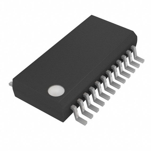
| 产品图片 |
|
| rohs | 符合RoHS无铅 / 符合限制有害物质指令(RoHS)规范要求 |
| 产品系列 | LED照明电子器件,LED照明驱动器,Texas Instruments TLC5928DBQR- |
| 数据手册 | |
| 产品型号 | TLC5928DBQR |
| 产品目录页面 | |
| 产品种类 | LED照明驱动器 |
| 低电平输出电流 | 1 mA |
| 供应商器件封装 | 24-SSOP/QSOP |
| 其它名称 | 296-23653-6 |
| 内部驱动器 | 是 |
| 功率耗散 | 1782 mW |
| 包装 | Digi-Reel® |
| 单位重量 | 129.500 mg |
| 商标 | Texas Instruments |
| 安装类型 | 表面贴装 |
| 安装风格 | SMD/SMT |
| 封装 | Reel |
| 封装/外壳 | 24-SSOP(0.154",3.90mm 宽) |
| 封装/箱体 | SSOP-24 |
| 工作温度 | -40°C ~ 85°C |
| 工作频率 | 35 MHz |
| 工厂包装数量 | 2500 |
| 恒压 | - |
| 恒流 | 是 |
| 拓扑 | - |
| 拓扑结构 | Boost |
| 最大工作温度 | + 85 C |
| 最大电源电流 | 2 mA |
| 最小工作温度 | - 40 C |
| 标准包装 | 1 |
| 电压-电源 | 3 V ~ 5.5 V |
| 电压-输出 | 17V |
| 类型 | Linear |
| 类型-初级 | 通用 |
| 类型-次级 | - |
| 系列 | TLC5928 |
| 输入电压 | 3 V to 5.5 V |
| 输出数 | 16 |
| 输出电流 | 35 mA |
| 输出端数量 | 16 Output |
| 输出类型 | Constant Current |
| 频率 | 35MHz |
| 高电平输出电流 | - 1 mA |


- 商务部:美国ITC正式对集成电路等产品启动337调查
- 曝三星4nm工艺存在良率问题 高通将骁龙8 Gen1或转产台积电
- 太阳诱电将投资9.5亿元在常州建新厂生产MLCC 预计2023年完工
- 英特尔发布欧洲新工厂建设计划 深化IDM 2.0 战略
- 台积电先进制程称霸业界 有大客户加持明年业绩稳了
- 达到5530亿美元!SIA预计今年全球半导体销售额将创下新高
- 英特尔拟将自动驾驶子公司Mobileye上市 估值或超500亿美元
- 三星加码芯片和SET,合并消费电子和移动部门,撤换高东真等 CEO
- 三星电子宣布重大人事变动 还合并消费电子和移动部门
- 海关总署:前11个月进口集成电路产品价值2.52万亿元 增长14.8%


PDF Datasheet 数据手册内容提取
TLC5928 www.ti.com SBVS120E–JULY2008–REVISEDJANUARY2011 16-Channel, Constant-Current LED Driver with LED Open Detection CheckforSamples:TLC5928 FEATURES APPLICATIONS 1 • 16Channels,Constant-CurrentSinkOutput • LEDVideoDisplays 23 withOn/OffControl • MessageBoards • 35-mACapability(Constant-CurrentSink) • Illumination • 10-nsHigh-SpeedConstant-CurrentSwitching DESCRIPTION TransientTime • LowOn-TimeError The TLC5928 is a 16-channel, constant-current sink LED driver. Each channel can be turned on/off by • LEDPower-SupplyVoltageupto17V writing serial data to an internal register. The • V =3.0Vto5.5V CC constant-current value of all 16 channels is set by a • Constant-CurrentAccuracy: singleexternalresistor. – Channel-to-Channel= ±1% The TLC5928 has two error detection circuits: one for – Device-to-Device=±1% LED open detection (LOD) and one for a pre-thermal warning (PTW). LOD detects a broken or • CMOSLogicLevelI/O disconnected LED and LEDs shorted to GND while • 35-MHzDataTransferRate the constant-current output is on. PTW indicates a • 20-nsBLANKPulseWidth hightemperaturecondition. • ReadableErrorInformation: – LEDOpenDetection(LOD) – Pre-ThermalWarning(PTW) • OperatingTemperature:–40°Cto+85°C VLED VLED VLED VLED ¼ ¼ ¼ ¼ ¼ ¼ ¼ ¼ OUT0 OUT15 OUT0 OUT15 DATA SIN SOUT SIN SOUT SCLK SCLK VCC SCLK VCC Controller LAT LAT VCC LAT VCC BLANK BLANK BLANK ERRERADOR IREF TLCIC51928 GND IREF TLCIC5n928 GND R R IREF IREF 3 TypicalApplicationCircuit(MultipleDaisy-ChainedTLC5928s) 1 Pleasebeawarethatanimportantnoticeconcerningavailability,standardwarranty,anduseincriticalapplicationsofTexas Instrumentssemiconductorproductsanddisclaimerstheretoappearsattheendofthisdatasheet. PowerPADisatrademarkofTexasInstruments,Inc. 2 Allothertrademarksarethepropertyoftheirrespectiveowners. 3 PRODUCTIONDATAinformationiscurrentasofpublicationdate. ©2008–2011,TexasInstrumentsIncorporated Products conform to specifications per the terms of the Texas Instruments standard warranty. Production processing does not necessarilyincludetestingofallparameters.
TLC5928 SBVS120E–JULY2008–REVISEDJANUARY2011 www.ti.com This integrated circuit can be damaged by ESD. Texas Instruments recommends that all integrated circuits be handled with appropriateprecautions.Failuretoobserveproperhandlingandinstallationprocedurescancausedamage. ESDdamagecanrangefromsubtleperformancedegradationtocompletedevicefailure.Precisionintegratedcircuitsmaybemore susceptibletodamagebecauseverysmallparametricchangescouldcausethedevicenottomeetitspublishedspecifications. PACKAGE/ORDERINGINFORMATION(1) PRODUCT PACKAGE-LEAD ORDERINGNUMBER TRANSPORTMEDIA,QUANTITY TLC5928DBQR TapeandReel,2500 TLC5928 SSOP-24/QSOP-24 TLC5928DBQ Tube,50 TLC5928PWR TapeandReel,2000 TLC5928 TSSOP-24 TLC5928PW Tube,60 TLC5928PWPR TapeandReel,2000 TLC5928 HTSSOP-24PowerPAD™ TLC5928PWP Tube,60 TLC5928RGER TapeandReel,3000 TLC5928 QFN-24 TLC5928RGE TapeandReel,250 (1) Forthemostcurrentpackageandorderinginformation,seethePackageOptionAddendumattheendofthisdocument,orvisitthe deviceproductfolderatwww.ti.com. ABSOLUTE MAXIMUM RATINGS(1)(2) Overoperatingfree-airtemperaturerange,unlessotherwisenoted. PARAMETER TLC5928 UNIT V Supplyvoltage:V –0.3to+6.0 V CC CC I Outputcurrent(dc) OUT0toOUT15 40 mA OUT V Inputvoltagerange SIN,SCLK,LAT,BLANK,IREF –0.3toV +0.3 V IN CC SOUT –0.3toV +0.3 V CC V Outputvoltagerange OUT OUT0toOUT15 –0.3to+18 V T Operatingjunctiontemperature +150 °C J(MAX) T Storagetemperaturerange –55to+150 °C STG Humanbodymodel(HBM) 2 kV ESDrating Chargeddevicemodel(CDM) 500 V (1) Stressesabovetheseratingsmaycausepermanentdamage.Exposuretoabsolutemaximumconditionsforextendedperiodsmay degradedevicereliability.Thesearestressratingsonly,andfunctionaloperationofthedeviceattheseoranyotherconditionsbeyond thosespecifiedisnotsupported. (2) Allvoltagevaluesarewithrespecttonetworkgroundterminal. DISSIPATION RATINGS OPERATINGFACTOR T <+25°C T =+70°C T =+85°C A A A PACKAGE ABOVET =+25°C POWERRATING POWERRATING POWERRATING A SSOP-24/QSOP-24 14.3mW/°C 1782mW 1140mW 927mW TSSOP-24 9.6mW/°C 1194mW 764mW 621mW HTSSOP-24(1) 28.9mW/°C 3611mW 2311mW 1878mW QFN-24(2) 24.8mW/°C 3106mW 1988mW 1615mW (1) WithPowerPADsolderedontocopperareaonprintedcircuitboard(PCB);2oz.copper.Formoreinformation,seeSLMA002(available fordownloadatwww.ti.com). (2) ThepackagethermalimpedanceiscalculatedinaccordancewithJESD51-5. 2 SubmitDocumentationFeedback ©2008–2011,TexasInstrumentsIncorporated ProductFolderLink(s):TLC5928
TLC5928 www.ti.com SBVS120E–JULY2008–REVISEDJANUARY2011 RECOMMENDED OPERATING CONDITIONS AtT =–40°Cto+85°C,unlessotherwisenoted. A TLC5928 PARAMETER TESTCONDITIONS MIN NOM MAX UNIT DCCharacteristics:V =3Vto5.5V CC V Supplyvoltage 3.0 5.5 V CC V Voltageappliedtooutput OUT0toOUT15 17 V O V High-levelinputvoltage 0.7×V V V IH CC CC V Low-levelinputvoltage GND 0.3×V V IL CC I High-leveloutputcurrent SOUT –1 mA OH I Low-leveloutputcurrent SOUT 1 mA OL I Constantoutputsinkcurrent OUT0toOUT15 2 35 mA OLC T Operatingfree-airtemperaturerange –40 +85 °C A T Operatingjunctiontemperaturerange –40 +125 °C J ACCharacteristics:V =3Vto5.5V CC f Datashiftclockfrequency SCLK 35 MHz CLK(SCLK) T SCLK 10 ns WH0 T SCLK 10 ns WL0 T Pulseduration LAT 20 ns WH1 T BLANK 20 ns WH2 T BLANK 20 ns WL2 T SIN–SCLK↑ 4 ns SU0 Setuptime T LAT↑–SCLK↑ 100 ns SU1 T SIN–SCLK↑ 3 ns H0 Holdtime T LAT↑–SCLK↑ 10 ns H1 ©2008–2011,TexasInstrumentsIncorporated SubmitDocumentationFeedback 3 ProductFolderLink(s):TLC5928
TLC5928 SBVS120E–JULY2008–REVISEDJANUARY2011 www.ti.com ELECTRICAL CHARACTERISTICS AtV =3.0Vto5.5VandT =–40°Cto+85°C.TypicalvaluesatV =3.3VandT =+25°C,unlessotherwisenoted. CC A CC A TLC5928 PARAMETER TESTCONDITIONS MIN TYP MAX UNIT VOH High-leveloutputvoltage IOH=–1mAatSOUT VCC–0.4 VCC V VOL Low-leveloutputvoltage IOL=1mAatSOUT 0 0.4 V IIN Inputcurrent VIN=VCCorGNDatSIN,SCLK,LAT,andBLANK –1 1 mA ICC1 SRIIRNE/FSC=L2K7/LkAΩT=low,BLANK=high,VOUTn=1V, 1 2 mA ICC2 SRIIRNE/FSC=L3Kk/LΩAT=low,BLANK=high,VOUTn=1V, 4.5 8 mA Supplycurrent(VCC) ICC3 SRIIRNE/FSC=L3Kk/LΩAT/BLANK=low,VOUTn=1V, 7 18 mA ICC4 SRIIRNE/FSC=L1K.5/LkAΩT/BLANK=low,VOUTn=1V, 16 40 mA IOLC Constantoutputcurrent A(sleleOUFiTgnur=eO6)N,,aVtOOUUTTn0=tVoOOUTUfiTx1=51V,RIREF=1.5kΩ 31 34 37 mA AllOUTnforconstant-currentdriver,alloutputsoff IOLKG Outputleakagecurrent BLANK=high,VOUTn=VOUTfix=17V,RIREF=1.5kΩ 0.1 mA (seeFigure6),atOUT0toOUT15 ΔIOLC C(cohnasntnaenlt--tcou-crrheanntneerlr)o(1r) AatllOOUUTT0nt=oOOUNT,V15OUTn=VOUTfix=1V,RIREF=1.5kΩ ±1 ±3 % ΔIOLC1 C(doenvsictaen-tto-c-duerrveicnet)e(2rr)or AatllOOUUTT0nt=oOOUNT,V15OUTn=VOUTfix=1V,RIREF=1.5kΩ ±1 ±6 % ΔIOLC2 Lineregulation(3) AatllOOUUTT0nt=oOOUNT,V15OUTn=VOUTfix=1V,RIREF=1.5kΩ ±0.5 ±1 %/V ΔIOLC3 Loadregulation(4) ARlIlROEFU=T1n.5=kOΩN,,aVtOOUUTnT=01toVOtUoT31V5,VOUTfix=1V, ±1 ±3 %/V T(PTW) Pre-thermalwarningthreshold Junctiontemperature(5) +125 +138 +150 °C VLOD LEDopendetectionthreshold AllOUTn=ON 0.25 0.30 0.35 V VIREF Referencevoltageoutput RIREF=1.5kΩ 1.16 1.20 1.24 V (1) ThedeviationofeachoutputfromtheaverageofOUT0–OUT15constant-current.Deviationiscalculatedbytheformula: I D(%) = OUTn -1 ´100 (I + I + ... + I + I ) OUT0 OUT1 OUT14 OUT15 16 . (2) ThedeviationoftheOUT0–OUT15constant-currentaveragefromtheidealconstant-currentvalue. Deviationiscalculatedbythefollowingformula: (I + I + ... I + I ) OUT0 OUT1 OUT14 OUT15 -(Ideal Output Current) 16 D(%) = ´100 Ideal Output Current Idealcurrentiscalculatedbytheformula: 1.20 I = 42´ OUT(IDEAL) R IREF (3) Lineregulationiscalculatedbythisequation: D(%/V) = (IOUTnat VCC= 5.5 V)-(IOUTnat VCC= 3.0 V) ´ 100 (I at V = 3.0 V) 5.5 V-3 V OUTn CC (4) Loadregulationiscalculatedbytheequation: (IOUTnat VOUTn= 3 V)-(IOUTnat VOUTn= 1 V) 100 D(%/V) = ´ (I at V = 1 V) 3 V-1 V OUTn OUTn (5) Nottested.Specifiedbydesign. 4 SubmitDocumentationFeedback ©2008–2011,TexasInstrumentsIncorporated ProductFolderLink(s):TLC5928
TLC5928 www.ti.com SBVS120E–JULY2008–REVISEDJANUARY2011 SWITCHING CHARACTERISTICS AtV =3.0Vto5.5V,T =–40°Cto+85°C,C =15pF,R =130Ω,R =1.5kΩ,andV =5.5V.Typicalvaluesat CC A L L IREF LED V =3.3VandT =+25°C,unlessotherwisenoted. CC A TLC5928 PARAMETER TESTCONDITIONS MIN TYP MAX UNIT t SOUT(seeFigure5) 5 15 ns R0 Risetime t OUTn(seeFigure4) 10 30 ns R1 t SOUT(seeFigure5) 5 15 ns F0 Falltime t OUTn(seeFigure4) 10 30 ns F1 t SCLK↑toSOUT 8 20 ns D0 LAT↑orBLANK↓toOUTnsinkcurrenton t 12 30 ns D1 Propagationdelaytime (seeFigure10) LAT↑orBLANK↑toOUTnsinkcurrentoff t 12 30 ns D2 (seeFigure10) t Outputon-timeerror(1) On/offlatchdata=all'1',20nsBLANKlowlevel –8 +8 ns ON_ERR one-shotpulseinput(seeFigure4) (1) Outputon-timeerror(t )iscalculatedbytheformula:t (ns)=t –BLANKlowlevelone-shotpulsewidth(T ). ON_ERR ON_ERR OUT_ON WL2 t indicatestheactualon-timeoftheconstant-currentdriver. OUT_ON FUNCTIONAL BLOCK DIAGRAM VCC VCC SIN LSB MSB On/Off Control Shift Register SCLK (1 Bit x 16 Channels) SOUT 0 15 16 LSB MSB 16 LAT On/Off Control Data Latch (1 Bit x 16 Channels) BLANK 0 15 16 SID Latch IREF 16-Channel Constant Current Sink Driver 16 Thermal Detection GND 16-Channel LED Open Detection GND ¼ OUT0 OUT1 OUT14 OUT15 ©2008–2011,TexasInstrumentsIncorporated SubmitDocumentationFeedback 5 ProductFolderLink(s):TLC5928
TLC5928 SBVS120E–JULY2008–REVISEDJANUARY2011 www.ti.com DEVICE INFORMATION SSOP-24/QSOP-24ANDTSSOP-24 HTSSOP-24PowerPAD DBQANDPWPACKAGES PWPPACKAGE (TOPVIEW) (TOPVIEW) GND 1 24 VCC GND 1 24 VCC SIN 2 23 IREF SIN 2 23 IREF SCLK 3 22 SOUT SCLK 3 22 SOUT LAT 4 21 BLANK LAT 4 21 BLANK OUT0 5 20 OUT15 OUT0 5 20 OUT15 OUT1 6 19 OUT14 OUT1 6 Thermal Pad 19 OUT14 TLC5928 (Bottom Side) OUT2 7 18 OUT13 OUT2 7 TLC5928 18 OUT13 OUT3 8 17 OUT12 OUT3 8 17 OUT12 OUT4 9 16 OUT11 OUT4 9 16 OUT11 OUT5 10 15 OUT10 OUT5 10 15 OUT10 OUT6 11 14 OUT9 OUT6 11 14 OUT9 OUT7 12 13 OUT8 OUT7 12 13 OUT8 QFN-24 RGEPACKAGE (TOPVIEW) CLK N ND CC EF OUT S SI G V R S I 4 3 2 1 0 9 2 2 2 2 2 1 LAT 1 18 BLANK OUT0 2 17 OUT15 OUT1 3 Thermal Pad 16 OUT14 (Bottom Side) OUT2 4 TLC5928 15 OUT13 OUT3 5 14 OUT12 OUT4 6 13 OUT11 7 8 9 10 11 12 5 6 7 8 9 0 T T T T T 1 U U U U U T O O O O O U O NOTE:ThermalpadisnotconnectedtoGNDinternally.ThethermalpadmustbeconnectedtoGNDviathePCBpattern. 6 SubmitDocumentationFeedback ©2008–2011,TexasInstrumentsIncorporated ProductFolderLink(s):TLC5928
TLC5928 www.ti.com SBVS120E–JULY2008–REVISEDJANUARY2011 TERMINALFUNCTIONS TERMINAL DBQ/PW/ NAME PWP RGE I/O DESCRIPTION Serialdatainputfordriveron/offcontrol.WhenSIN=highlevel,data'1'arewrittenintoLSB SIN 2 23 I oftheon/offcontrolshiftregisterattherisingedgeofSCLK. Serialdatashiftclock.Schmittbufferinput.Alldataintheon/offcontrolshiftregisterare SCLK 3 24 I shiftedtowardtheMSBby1-bitsynchronizationofSCLK.ArisingedgeonSCLKisallowed 100nsafterarisingedgeofLAT. Edgetriggeredlatch.Thedataintheon/offcontroldatashiftregisteraretransferredtothe on/offcontroldatalatchatthisrisingedge.Atthesametime,thedataintheon/offcontrolshift LAT 4 1 I registerarereplacedwithLEDopendetection(LOD)andpre-thermalwarning(PTW)data. LATmustbetoggledonlyonceaftertheshiftdataareupdatedtoavoidtheon/offcontrollatch databeingreplacedwithLODandPTWdataintheshiftregister. Blank,alloutputs.WhenBLANK=highlevel,allconstant-currentoutputs(OUT0–OUT15)are forcedoff.WhenBLANK=lowlevel,allconstant-currentoutputsarecontrolledbytheon/off BLANK 21 18 I controldatainthedatalatch.LODandPTWdataarelatchedintotheSIDdatalatchatthe risingedgeofBLANKandarepresentattheoutputoftheSIDdatalatchwhenBLANKislow. Constant-currentvaluesetting,OUT0–OUT15sinkconstant-currentissettodesiredvalueby IREF 23 20 I/O connectiontoanexternalresistorbetweenIREFandGND. Serialdataoutput.ThisoutputisconnectedtotheMSBoftheon/offdatashiftregister.SOUT SOUT 22 19 O datachangesattherisingedgeofSCLK. Constant-currentoutput.Eachoutputcanbetiedtogetherwithotherstoincreasethe OUT0 5 2 O constant-current.Differentvoltagescanbeappliedtoeachoutput. OUT1 6 3 O Constant-currentoutput OUT2 7 4 O Constant-currentoutput OUT3 8 5 O Constant-currentoutput OUT4 9 6 O Constant-currentoutput OUT5 10 7 O Constant-currentoutput OUT6 11 8 O Constant-currentoutput OUT7 12 9 O Constant-currentoutput OUT8 13 10 O Constant-currentoutput OUT9 14 11 O Constant-currentoutput OUT10 15 12 O Constant-currentoutput OUT11 16 13 O Constant-currentoutput OUT12 17 14 O Constant-currentoutput OUT13 18 15 O Constant-currentoutput OUT14 19 16 O Constant-currentoutput OUT15 20 17 O Constant-currentoutput VCC 24 21 — Power-supplyvoltage GND 1 22 — Powerground ©2008–2011,TexasInstrumentsIncorporated SubmitDocumentationFeedback 7 ProductFolderLink(s):TLC5928
TLC5928 SBVS120E–JULY2008–REVISEDJANUARY2011 www.ti.com PARAMETER MEASUREMENT INFORMATION PIN EQUIVALENT INPUT AND OUTPUT SCHEMATIC DIAGRAMS VCC VCC INPUT SOUT GND GND Figure1.SIN,SCLK,LAT,BLANK Figure2.SOUT OUTn GND Figure3.OUT0ThroughOUT15 TEST CIRCUITS VCC R L VCC VCC IREF OUTn V RIREF GND CL(1) LED VCC SOUT GND CL(1) (1) C includesmeasurementprobeandjigcapacitance. L (1) C includesmeasurementprobeandjigcapacitance. Figure4. RiseTimeandFallTimeTestCircuitfor L OUTn Figure5. RiseTimeandFallTimeTestCircuitfor SOUT VCC OUT0 VCC ¼ IREF OUTn ¼ RIREF GND OUT15 VOUTn VOUT FIX Figure6.Constant-CurrentTestCircuitforOUTn 8 SubmitDocumentationFeedback ©2008–2011,TexasInstrumentsIncorporated ProductFolderLink(s):TLC5928
TLC5928 www.ti.com SBVS120E–JULY2008–REVISEDJANUARY2011 TIMING DIAGRAMS T , T , T , T , T : WH0 WL0 WH1 WH2 WL2 V CC INPUT(1) 50% GND T T WH WL T , T , T , T : SU0 SU1 H0 H1 V CC CLOCK 50% INPUT(1) GND T T SU H V CC DATA/CONTROL 50% INPUT(1) GND (1) Inputpulseriseandfalltimeis1nsto3ns. Figure7. InputTiming t , t , t , t , t , t , t : R0 R1 F0 F1 D0 D1 D2 V CC INPUT(1) 50% GND t D V or V 90% OH OUTn OUTPUT 50% 10% V or V OL OUTn t or t R F (1) Inputpulseriseandfalltimeis1nsto3ns. Figure8. OutputTiming ©2008–2011,TexasInstrumentsIncorporated SubmitDocumentationFeedback 9 ProductFolderLink(s):TLC5928
TLC5928 SBVS120E–JULY2008–REVISEDJANUARY2011 www.ti.com SIN DATA DATA DATA DATA DATA DATA DATA DATA DATA DATA DATA DATA DATA DATA DATA DATA 0A 15B 14B 13B 12B 11B 3B 2B 1B 0B 15C 14C 13C 12C 11C 10C T TSU0 H0 T TH1 WH0 T SU1 SCLK 1 2 3 4 5 13 14 15 16 1 2 3 4 5 6 T T WH1 WL0 LAT Shift Register DATA LOD DATA DATA DATA DATA DATA DATA DATA DATA LOD 0A or PTW_A DATA DATA DATA DATA DATA LSB Data (Internal) 0A 0 15B 14B 13B 12B 3B 2B 1B 0B 15C 14C 13C 12C 11C Shift Register DATA LOD LOD DATA DATA DATA DATA DATA DATA LOD 1A or PTW_A LOD DATA DATA DATA DATA LSB+1 Data (Internal) 1A 1 0 15B 14B 13B 4B 3B 2B 0A 15C 14C 13C 12C ¼ ¼ ¼ Shift Register DATA LOD LOD LOD LOD LOD LOD LOD DATA LOD 14A or PTW_A LOD LOD LOD LOD LOD MSB-1 Data (Internal) 14A 14 13 12 11 10 1 0 15B 13A 12A 11A 10A 9A Shift Register DATA LOD LOD LOD LOD LOD LOD LOD LOD DATA LOD 15A or PTW_A LOD LOD LOD LOD LOD MSB Data (Internal) 15A 15 14 13 12 11 2 1 0 15B 14A 13A 12A 11A 10A On/Off Control Previous On/Off Latch Data LatestOn/OffLatch Data Latch Data (Internal) SOUT DATA LOD LOD LOD LOD LOD LOD LOD LOD DATA LOD 15A or PTW_A LOD LOD LOD LOD LOD 15A 15 14 13 12 11 2 1 0 15B 14A 13A 12A 11A 10A t t /t D0 R0 F0 t WH2 BLANK t WL2 t t D1 D2 OFF OFF OUTn(1) ON ON ON t tD1 tD2 OFF OUTON OFF OUTn(2) ON ON t t F1 D1 OFF OFF OUTn(3) ON ON t OFF R1 OFF OUTn(4) ON (1) On/offlatcheddataare'1'. (2) On/offlatcheddataarechangedfrom'1'to'0'atthesecondLATsignal. (3) On/offlatcheddataarechangedfrom'0'to'1'atthesecondLATsignal. (4) On/offlatcheddataare'0'. Figure9. TimingDiagram 10 SubmitDocumentationFeedback ©2008–2011,TexasInstrumentsIncorporated ProductFolderLink(s):TLC5928
TLC5928 www.ti.com SBVS120E–JULY2008–REVISEDJANUARY2011 TYPICAL CHARACTERISTICS AtV =3.3VandT =+25°C,unlessotherwisenoted. CC A REFERENCERESISTOR POWERDISSIPATIONRATE vsOUTPUTCURRENT vsFREE-AIRTEMPERATURE 100000 4000 TLC5928PWP W) Wor () 25200 ate (m 3000 TLC5928RGE st R Reference Resi 10000 10080 5040 3360 2520 2016 1680 Power Dissipation 21000000 TLC5928TDLBCQ5928PW 1440 1000 0 0 5 10 15 20 25 30 35 -40 -20 0 20 40 60 80 100 Output Current (mA) Free-Air Temperature (°C) Figure10. Figure11. OUTPUTCURRENTvs OUTPUTCURRENTvs OUTPUTVOLTAGE OUTPUTVOLTAGE 40 40 TA= +25°C IO= 35 mA 39 IO= 30 mA 35 IO= 30 mA 38 mA) 30 mA) 37 urrent ( 2250 IO= 20 mA urrent ( 3365 C C ut 15 ut 34 p p Out 10 IO= 10 mA Out 33 TA=-40°C 5 IO= 2 mA IO= 5 mA 3321 TTA== ++2855°°CC A 0 30 0 0.5 1.0 1.5 2.0 2.5 3.0 0 0.5 1.0 1.5 2.0 2.5 3.0 Output Voltage (V) Output Voltage (V) Figure12. Figure13. ΔI vsAMBIENTTEMPERATURE ΔI vsOUTPUTCURRENT OLC OLC 4 4 I = 35 mA T = +25°C O A 3 3 2 2 1 1 %) %) ( ( C 0 C 0 OL OL DI -1 DI -1 -2 -2 V = 3.3 V V = 3.3 V -3 CC -3 CC V = 5 V V = 5 V CC CC -4 -4 -40 -20 0 20 40 60 80 100 0 10 20 30 40 Ambient Temperature (°C) Output Current (mA) Figure14. Figure15. ©2008–2011,TexasInstrumentsIncorporated SubmitDocumentationFeedback 11 ProductFolderLink(s):TLC5928
TLC5928 SBVS120E–JULY2008–REVISEDJANUARY2011 www.ti.com TYPICAL CHARACTERISTICS (continued) AtV =3.3VandT =+25°C,unlessotherwisenoted. CC A CONSTANT-CURRENTOUTPUT VOLTAGEWAVEFORM CH1-BLANK CH1 (2 V/div) (20 ns) CH2-OUT0 CH2 (2 V/div) (BLANK = 20 ns) I = 35 mA CH3-OUT15 OLC CH3 (2 V/div) T = +25°C (BLANK = 20 ns) A R = 130W L C = 15 pF L VLED = 5.5 V Time (12.5 ns/div) Figure16. 12 SubmitDocumentationFeedback ©2008–2011,TexasInstrumentsIncorporated ProductFolderLink(s):TLC5928
TLC5928 www.ti.com SBVS120E–JULY2008–REVISEDJANUARY2011 DETAILED DESCRIPTION SETTING FOR THE CONSTANT SINK CURRENT VALUE The constant-current values are determined by an external resistor (R ) placed between IREF and GND. The IREF resistor(R )valueiscalculatedbyEquation1. IREF V (V) R (kW) = IREF ´42 IREF I (mA) OLC Where: V =theinternalreferencevoltageontheIREFpin(typically1.20V) (1) IREF I must be set in the range of 2 mA to 35 mA. The constant sink current characteristic for the external resistor OLC valueisshowninFigure10.Table1describestheconstant-currentoutputversusexternalresistorvalue. Table1.Constant-CurrentOutputversusExternalResistorValue I (mA,Typical) R (kΩ) OLCMax IREF 35 1.44 30 1.68 25 2.02 20 2.52 15 3.36 10 5.04 5 10.1 2 25.2 CONSTANT-CURRENT DRIVER ON/OFF CONTROL When BLANK is low, the corresponding output is turned on if the data in the on/off control data latch are '1' and remainsoffifthedataare'0'.WhenBLANKishigh,alloutputsareforcedoff.ThiscontrolisshowninTable2. Table2.On/OffControlDataTruthTable ON/OFFCONTROLLATCHDATA CONSTANT-CURRENTOUTPUTSTATUS 0 Off 1 On When the IC is initially powered on, the data in the on/off control shift register and data latch are not set to the respective default value. Therefore, the on/off control data must be written to the data latch before turning the constant-current output on. BLANK should be at a high level when powered on because the constant-current maybeturnedonasaresultofrandomdataintheon/offcontrollatch. The on/off data corresponding to any unconnected OUTn outputs should be set to ‘0’ before turning on the remainingoutputs.Otherwise,thesupplycurrent(I )increaseswhiletheLEDsareon. CC ©2008–2011,TexasInstrumentsIncorporated SubmitDocumentationFeedback 13 ProductFolderLink(s):TLC5928
TLC5928 SBVS120E–JULY2008–REVISEDJANUARY2011 www.ti.com REGISTER CONFIGURATION The TLC5928 has an on/off control data shift register and data latch. Both the on/off control shift register and latch are 16 bits long and are used to turn on/off the constant-current drivers. Figure 17 shows the shift register and latch configuration. The data at the SIN pin are shifted in to the LSB of the shift register at the rising edge of the SCLK pin; SOUT data change at the rising edge of SCLK. The timing diagram for data writing is shown in Figure18.Thedriveron/offiscontrolledbythedataintheon/offcontroldatalatch. The on/off data are latched into the data latch by a rising edge of LAT after the data are written into the on/off control shift register by SIN and SCLK. At the same time, the data in the on/off control shift register are replaced with LED open detection (LOD) and pre-thermal warning (PTW) data. Therefore, LAT must be input only once after the on/off data update to avoid the on/off control data latch being replaced with LOD and PTW data in the shift register. When the IC is initially powered on, the data in the on/off control shift register and latch are not set to the default values; on/off control data must be written to the on/off control data latch before turning the constant-current output on. BLANK should be high when the IC is powered on because the constant-current may be turned on at that time as a result of random values in the on/off data latch. All constant-current outputs are forcedoffwhenBLANKishigh. On/Off Control Shift Register (1 Bit´16 Channels) MSB LSB 15 14 13 12 11 4 3 2 1 0 On/Off Data On/Off Data On/Off Data On/Off Data ¼ On/Off Data On/Off Data On/Off Data On/Off Data SIN SOUT for for for for for for for for OUT15 OUT14 OUT13 OUT12 OUT3 OUT2 OUT1 OUT0 SCLK ¼ MSB LSB 15 14 13 12 11 4 3 2 1 0 On/Off Data On/Off Data On/Off Data On/Off Data ¼ On/Off Data On/Off Data On/Off Data On/Off Data for for for for for for for for LAT OUT15 OUT14 OUT13 OUT12 OUT3 OUT2 OUT1 OUT0 On/Off Control Data Latch (1 Bit´16 Channels) 16 Bits To Constant Current Driver Control Block Figure17. On/OffControlShiftRegisterandLatchConfiguration 14 SubmitDocumentationFeedback ©2008–2011,TexasInstrumentsIncorporated ProductFolderLink(s):TLC5928
TLC5928 www.ti.com SBVS120E–JULY2008–REVISEDJANUARY2011 SIN DATA DATA DATA DATA DATA DATA DATA DATA DATA DATA DATA DATA DATA DATA DATA DATA 0A 15B 14B 13B 12B 11B 3B 2B 1B 0B 15C 14C 13C 12C 11C 10C SCLK 1 2 3 4 5 13 14 15 16 1 2 3 4 5 6 LAT Shift Register DATA LOD DATA DATA DATA DATA DATA DATA DATA DATA LOD 0A or PTW_A DATA DATA DATA DATA DATA LSB Data (Internal) 0A 0 15B 14B 13B 12B 3B 2B 1B 0B 15C 14C 13C 12C 11C Shift Register DATA LOD LOD DATA DATA DATA DATA DATA DATA LOD 1A or PTW_A LOD DATA DATA DATA DATA LSB+1 Data (Internal) 1A 1 0 15B 14B 13B 4B 3B 2B 0A 15C 14C 13C 12C ¼ ¼ ¼ MSB-1 DSahtiaft( RInetegrinstael)r D1A4TAA L1O4D L1O3D L1O2D L1O1D L1O0D LO1D LO0D D1A5TBA LOD 14A or PTW_A L1O3AD L1O2AD L1O1AD L1O0AD L9OAD Shift Register DATA LOD LOD LOD LOD LOD LOD LOD LOD DATA LOD 15A or PTW_A LOD LOD LOD LOD LOD MSB Data(Internal) 1A 15 14 13 12 11 2 1 0 15B 14A 13A 12A 11A 10A On/Off Control Previous On/Off Latch Data LatestOn/OffLatch Data Latch Data (Internal) SOUT DATA LOD LOD LOD LOD LOD LOD LOD LOD DATA LOD 15A or PTW_A LOD LOD LOD LOD LOD 1A 15 14 13 12 11 2 1 0 15B 14A 13A 12A 11A 10A BLANK OFF OUTn(1) OFF ON ON OFF OUTn(2) OFF ON ON OUTn(3) OFF OFF OFF ON ON OFF OFF OUTn(4) OFF ON (1) On/offlatcheddataare'1'. (2) On/offlatcheddataarechangedfrom'1'to'0'atthesecondLATsignal. (3) On/offlatcheddataarechangedfrom'0'to'1'atthesecondLATsignal. (4) On/offlatcheddataare'0'. Figure18. On/OffControlOperation ©2008–2011,TexasInstrumentsIncorporated SubmitDocumentationFeedback 15 ProductFolderLink(s):TLC5928
TLC5928 SBVS120E–JULY2008–REVISEDJANUARY2011 www.ti.com LED OPEN DETECTION (LOD) AND PRE-THERMAL WARNING (PTW) The LED open detection (LOD) circuit checks the voltage of each active (that is, on) constant-current sink output (OUT0throughOUT15)todetectopenLEDsandLEDsshortedtoGNDwhileBLANKislow.TheLODbitsinthe status information data register (SID) are set to '1' if the voltage of the corresponding OUTn pin is less than the LED open detection threshold (V = 0.3 V, typ). The status information data can be read from the SOUT pin. LOD To avoid false detection of open LEDs, the LED driver design must ensure that the constant-current sink output voltage is greater than 0.3 V when the outputs are on. Also, the output on-time must be 1 ms or greater to correctlyreadthevalidLODstatus. The PTW function indicates that the IC junction temperature is too high. The PTW bit in the SID data is set to '1' while the IC junction temperature exceeds the temperature threshold (T = +138 °C, typ). If the IC junction (PTW) temperature decreases below the temperature of T , the SID data are set depending on the LOD function. (PTW) The constant-current outputs are not forced off during PTW conditions, so the controller should take appropriate action(suchasreducingthedutycycleofeffectedchannels). The LOD and PTW data are latched into the SID latch with the rising edge of BLANK and do not change until BLANK goes low. The SID data latched in the latch are transferred into the on/off shift register with a rising edge of LAT. SID can be shifted out from SOUT with rising edges of SCLK. The data in the on/off control shift register are replaced with the LOD and PTW data at the rising edge of LAT. Therefore, LAT should be input only once after the shift data are updated to avoid the on/off control data latch information from being replaced with LOD andPTWdataintheshiftregister.AtimingdiagramforLOD,PTW,andSIDisshowninFigure19. BLANK OUTn OFF OUTn OUTn ON V OUTn If the voltage of OUTn (V ) is less than V (0.3 V, typ) when OUTn is on, GND OUTn LOD then the LOD circuit reports error information to the LOD data latch and the error information is set as '1' to the bit that corresponds with LOD circuit needs 1ms to detect LED the error OUTn in the LOD data latch. open correctly as maximum. LOD Circuit Data No Error Information Latest Error Information From LOD Circuit No Error Information (Internal) LOD and PTW data are always copied into T < T : SID data latch while BLANK is low level. T < T : PTW Circuit Data J (PTW) J (PTW) (Internal) Normal Temperature TJ³T(PTW): High Temperature Normal Temperature LOD and PTW data of from before BLANK goes high are held in the Previous LOD and PTW Data SID data latch at the rising edge of BLANK. SID Data Latch PTW Error Latest Error Information From LOD and PTW Circuit (Internal) No Error Information Figure19. LOD/PTW/SIDtiming 16 SubmitDocumentationFeedback ©2008–2011,TexasInstrumentsIncorporated ProductFolderLink(s):TLC5928
TLC5928 www.ti.com SBVS120E–JULY2008–REVISEDJANUARY2011 STATUS INFORMATION DATA (SID) ThelatchedLEDopendetection(LOD)errorandpre-thermalwarning(PTW)intheSIDdatalatchareshiftedout onto the SOUT pin with each rising edge of SCLK. If a PTW is reported, all LOD error bits are set to '1'. The SID data are written over the data in the on/off control shift register at the rising edge of LAT. Therefore, the previous data in the on/off control shift register are lost when SID information is latched in. Figure 20 shows the SID bit assignments.SeeFigure7forthereadtimingofSID. When the IC is powered on, the initial LOD data are invalid. Therefore, LOD data must be read after the rising edgeofBLANK.Table3showsatruthtableforLODandPTW. Table3.LODandPTWTruthTable CONDITION SIDDATA LEDisconnected(V >V ) '0'(lowlevelatSOUT) OUTn LOD LEDopendetection(LODn) LEDisopenedorshortedtoGND '1'(highlevelatSOUT);settothebitthathasan (V ≤V andoutputon) LEDerrorcondition OUTn LOD ICtemperatureislow(ICtemperature≤T ) DependLEDopenerror (PTW) Pre-thermalwarning(PTW) ICtemperatureishigh(ICtemperature>T ) Allbits='1'(highlevelatSOUT) (PTW) SID Data Latch (1 Bit´16 Channels) MSB LSB 15 14 13 12 11 4 3 2 1 0 OUT15 OUT15 OUT15 OUT15 ¼ OUT15 OUT15 OUT15 OUT15 LOD Data LOD Data LOD Data LOD Data LOD Data LOD Data LOD Data LOD Data (LOD 15) (LOD 14) (LOD 13) (LOD 12) (LOD 3) (LOD 2) (LOD 1) (LOD 0) All Bits Become‘1’When the IC is in a PTW (Pre-Thermal Warning) Condition ¼ MSB LSB 15 14 13 12 11 4 3 2 1 0 On/Off Data On/Off Data On/Off Data On/Off Data ¼ On/Off Data On/Off Data On/Off Data On/Off Data SIN SOUT for for for for for for for for OUT15 OUT14 OUT13 OUT12 OUT3 OUT2 OUT1 OUT0 SCLK The 16 bits in the SID latch are loaded into the on/off shift register at the rising edge of LAT. SID Control Shift Register (1 Bit´16 Channels) Figure20. StatusInformationDataConfiguration LAYOUT CONSIDERATIONS The output current transient time in the TLC5928 is very fast. In addition, all outputs turn on or off at the same time to minimize the output on-time error. This high current demand can cause GND to shift in the entire system, and lead to false triggering of signals. To overcome this issue, design all GND lines to be as wide and short as possibleinordertoreduceparasiticinductanceandresistance. ©2008–2011,TexasInstrumentsIncorporated SubmitDocumentationFeedback 17 ProductFolderLink(s):TLC5928
TLC5928 SBVS120E–JULY2008–REVISEDJANUARY2011 www.ti.com REVISION HISTORY NOTE:Pagenumbersforpreviousrevisionsmaydifferfrompagenumbersinthecurrentversion. ChangesfromRevisionD(August2010)toRevisionE Page • AddedLayoutConsiderationssection ................................................................................................................................ 17 ChangesfromRevisionC(November2008)toRevisionD Page • ChangedSO-24toSSOP-24/QSOP-24inPackage/OrderingInformationtable ................................................................. 2 • ChangedSO-24toSSOP-24/QSOP-24inDissipationRatingstable .................................................................................. 2 • Updatedfunctionalblockdiagram ........................................................................................................................................ 5 • ChangedSO-24toSSOP-24/QSOP-24inDBQandPWPackagespinout......................................................................... 6 • UpdatedFigure9 ................................................................................................................................................................ 10 • UpdatedFigure18 .............................................................................................................................................................. 15 18 SubmitDocumentationFeedback ©2008–2011,TexasInstrumentsIncorporated ProductFolderLink(s):TLC5928
PACKAGE OPTION ADDENDUM www.ti.com 6-Feb-2020 PACKAGING INFORMATION Orderable Device Status Package Type Package Pins Package Eco Plan Lead/Ball Finish MSL Peak Temp Op Temp (°C) Device Marking Samples (1) Drawing Qty (2) (6) (3) (4/5) HPA00534DBQR ACTIVE SSOP DBQ 24 2500 Green (RoHS NIPDAU Level-2-260C-1 YEAR -40 to 85 TLC5928 & no Sb/Br) TLC5928DBQ ACTIVE SSOP DBQ 24 50 Green (RoHS NIPDAU Level-2-260C-1 YEAR -40 to 85 TLC5928 & no Sb/Br) TLC5928DBQR ACTIVE SSOP DBQ 24 2500 Green (RoHS NIPDAU Level-2-260C-1 YEAR -40 to 85 TLC5928 & no Sb/Br) TLC5928PW ACTIVE TSSOP PW 24 60 Green (RoHS NIPDAU Level-1-260C-UNLIM -40 to 85 PJ5928 & no Sb/Br) TLC5928PWP ACTIVE HTSSOP PWP 24 60 Green (RoHS NIPDAU Level-2-260C-1 YEAR -40 to 85 PJ5928 & no Sb/Br) TLC5928PWPR ACTIVE HTSSOP PWP 24 2000 Green (RoHS NIPDAU Level-2-260C-1 YEAR -40 to 85 PJ5928 & no Sb/Br) TLC5928PWR ACTIVE TSSOP PW 24 2000 Green (RoHS NIPDAU Level-1-260C-UNLIM -40 to 85 PJ5928 & no Sb/Br) TLC5928RGER ACTIVE VQFN RGE 24 3000 Green (RoHS NIPDAU Level-2-260C-1 YEAR -40 to 85 TLC & no Sb/Br) 5928 TLC5928RGET ACTIVE VQFN RGE 24 250 Green (RoHS NIPDAU Level-2-260C-1 YEAR -40 to 85 TLC & no Sb/Br) 5928 (1) The marketing status values are defined as follows: ACTIVE: Product device recommended for new designs. LIFEBUY: TI has announced that the device will be discontinued, and a lifetime-buy period is in effect. NRND: Not recommended for new designs. Device is in production to support existing customers, but TI does not recommend using this part in a new design. PREVIEW: Device has been announced but is not in production. Samples may or may not be available. OBSOLETE: TI has discontinued the production of the device. (2) RoHS: TI defines "RoHS" to mean semiconductor products that are compliant with the current EU RoHS requirements for all 10 RoHS substances, including the requirement that RoHS substance do not exceed 0.1% by weight in homogeneous materials. Where designed to be soldered at high temperatures, "RoHS" products are suitable for use in specified lead-free processes. TI may reference these types of products as "Pb-Free". RoHS Exempt: TI defines "RoHS Exempt" to mean products that contain lead but are compliant with EU RoHS pursuant to a specific EU RoHS exemption. Green: TI defines "Green" to mean the content of Chlorine (Cl) and Bromine (Br) based flame retardants meet JS709B low halogen requirements of <=1000ppm threshold. Antimony trioxide based flame retardants must also meet the <=1000ppm threshold requirement. (3) MSL, Peak Temp. - The Moisture Sensitivity Level rating according to the JEDEC industry standard classifications, and peak solder temperature. Addendum-Page 1
PACKAGE OPTION ADDENDUM www.ti.com 6-Feb-2020 (4) There may be additional marking, which relates to the logo, the lot trace code information, or the environmental category on the device. (5) Multiple Device Markings will be inside parentheses. Only one Device Marking contained in parentheses and separated by a "~" will appear on a device. If a line is indented then it is a continuation of the previous line and the two combined represent the entire Device Marking for that device. (6) Lead/Ball Finish - Orderable Devices may have multiple material finish options. Finish options are separated by a vertical ruled line. Lead/Ball Finish values may wrap to two lines if the finish value exceeds the maximum column width. Important Information and Disclaimer:The information provided on this page represents TI's knowledge and belief as of the date that it is provided. TI bases its knowledge and belief on information provided by third parties, and makes no representation or warranty as to the accuracy of such information. Efforts are underway to better integrate information from third parties. TI has taken and continues to take reasonable steps to provide representative and accurate information but may not have conducted destructive testing or chemical analysis on incoming materials and chemicals. TI and TI suppliers consider certain information to be proprietary, and thus CAS numbers and other limited information may not be available for release. In no event shall TI's liability arising out of such information exceed the total purchase price of the TI part(s) at issue in this document sold by TI to Customer on an annual basis. Addendum-Page 2
PACKAGE MATERIALS INFORMATION www.ti.com 9-Mar-2018 TAPE AND REEL INFORMATION *Alldimensionsarenominal Device Package Package Pins SPQ Reel Reel A0 B0 K0 P1 W Pin1 Type Drawing Diameter Width (mm) (mm) (mm) (mm) (mm) Quadrant (mm) W1(mm) TLC5928PWR TSSOP PW 24 2000 330.0 16.4 6.95 8.3 1.6 8.0 16.0 Q1 TLC5928RGER VQFN RGE 24 3000 330.0 12.4 4.25 4.25 1.15 8.0 12.0 Q2 TLC5928RGET VQFN RGE 24 250 180.0 12.4 4.25 4.25 1.15 8.0 12.0 Q2 PackMaterials-Page1
PACKAGE MATERIALS INFORMATION www.ti.com 9-Mar-2018 *Alldimensionsarenominal Device PackageType PackageDrawing Pins SPQ Length(mm) Width(mm) Height(mm) TLC5928PWR TSSOP PW 24 2000 367.0 367.0 38.0 TLC5928RGER VQFN RGE 24 3000 367.0 367.0 35.0 TLC5928RGET VQFN RGE 24 250 210.0 185.0 35.0 PackMaterials-Page2
GENERIC PACKAGE VIEW PWP 24 PowerPADTM TSSOP - 1.2 mm max height 4.4 x 7.6, 0.65 mm pitch PLASTIC SMALL OUTLINE This image is a representation of the package family, actual package may vary. Refer to the product data sheet for package details. 4224742/B www.ti.com
PACKAGE OUTLINE PWP0024B PowerPAD T M TSSOP - 1.2 mm max height SCALE 2.200 PLASTIC SMALL OUTLINE 6.6 TYP SEATING PLANE C 6.2 PIN 1 ID A AREA 0.1 C 22X 0.65 24 1 7.9 2X 7.7 7.15 NOTE 3 12 13 0.30 4.5 24X B 0.19 4.3 0.1 C A B (0.15) TYP SEE DETAIL A 4X (0.2) MAX 2X (0.95) MAX NOTE 5 NOTE 5 EXPOSED THERMAL PAD 0.25 5.16 GAGE PLANE 1.2 MAX 4.12 0.15 0 - 8 0.05 0.75 0.50 DETAIL A (1) TYPICAL 2.40 1.65 4222709/A 02/2016 PowerPAD is a trademark of Texas Instruments. NOTES: 1. All linear dimensions are in millimeters. Any dimensions in parenthesis are for reference only. Dimensioning and tolerancing per ASME Y14.5M. 2. This drawing is subject to change without notice. 3. This dimension does not include mold flash, protrusions, or gate burrs. Mold flash, protrusions, or gate burrs shall not exceed 0.15 mm per side. 4. Reference JEDEC registration MO-153. 5. Features may not be present and may vary. www.ti.com
EXAMPLE BOARD LAYOUT PWP0024B PowerPAD T M TSSOP - 1.2 mm max height PLASTIC SMALL OUTLINE (3.4) NOTE 9 SOLDER MASK DEFINED PAD (2.4) 24X (1.5) SYMM SEE DETAILS 1 24 24X (0.45) (R0.05) TYP (1.1) (7.8) SYMM TYP NOTE 9 (5.16) 22X (0.65) ( 0.2) TYP VIA 12 13 METAL COVERED (1) TYP BY SOLDER MASK (5.8) LAND PATTERN EXAMPLE SCALE:10X SOOPLEDNEINRG MASK METAL SMOELTDAELR U MNDAESRK SOOPLEDNEINRG MASK 0.05 MIN 0.05 MAX ALL AROUND ALL AROUND NON SOLDER MASK SOLDER MASK DEFINED DEFINED SOLDER MASK DETAILS PADS 1-24 4222709/A 02/2016 NOTES: (continued) 6. Publication IPC-7351 may have alternate designs. 7. Solder mask tolerances between and around signal pads can vary based on board fabrication site. 8. This package is designed to be soldered to a thermal pad on the board. For more information, see Texas Instruments literature numbers SLMA002 (www.ti.com/lit/slma002) and SLMA004 (www.ti.com/lit/slma004). 9. Size of metal pad may vary due to creepage requirement. www.ti.com
EXAMPLE STENCIL DESIGN PWP0024B PowerPAD T M TSSOP - 1.2 mm max height PLASTIC SMALL OUTLINE (2.4) BASED ON 0.125 THICK 24X (1.5) STENCIL (R0.05) TYP 1 24 24X (0.45) (5.16) SYMM BASED ON 0.125 THICK STENCIL 22X (0.65) 12 13 SYMM METAL COVERED BY SOLDER MASK SEE TABLE FOR DIFFERENT OPENINGS (5.8) FOR OTHER STENCIL THICKNESSES SOLDER PASTE EXAMPLE EXPOSED PAD 100% PRINTED SOLDER COVERAGE BY AREA SCALE:10X STENCIL SOLDER STENCIL THICKNESS OPENING 0.1 2.68 X 5.77 0.125 2.4 X 5.16 (SHOWN) 0.15 2.19 X 4.71 0.175 2.03 X 4.36 4222709/A 02/2016 NOTES: (continued) 10. Laser cutting apertures with trapezoidal walls and rounded corners may offer better paste release. IPC-7525 may have alternate design recommendations. 11. Board assembly site may have different recommendations for stencil design. www.ti.com
GENERIC PACKAGE VIEW RGE 24 VQFN - 1 mm max height PLASTIC QUAD FLATPACK - NO LEAD Images above are just a representation of the package family, actual package may vary. Refer to the product data sheet for package details. 4204104/H
PACKAGE OUTLINE RGE0024C VQFN - 1 mm max height PLASTIC QUAD FLATPACK- NO LEAD A 4.1 B 3.9 4.1 PIN 1 INDEX AREA 3.9 1 MAX C SEATING PLANE 0.05 0.00 2X 2.5 0.08 C 2.1±0.1 (0.2) TYP 7 12 20X 0.5 6 13 2X 25 SYMM 2.5 1 18 0.30 PIN 1 ID 24X 0.18 (OPTIONAL) 24 19 0.1 C A B SYMM 0.50 0.05 C 24X 0.30 4224376 A 072018 NOTES: 1. All linear dimensions are in millimeters. Any dimensions in parenthesis are for reference only. Dimensioning and tolerancing per ASME Y14.5M. 2. This drawing is subject to change without notice. 3. The package thermal pad must be soldered to the printed circuit board for thermal and mechanical performance. www.ti.com
EXAMPLE BOARD LAYOUT RGE0024C VQFN - 1 mm max height PLASTIC QUAD FLATPACK- NO LEAD (3.8) ( 2.1) 24 19 24X (0.6) 24X (0.24) 1 18 20X (0.5) 25 SYMM (3.8) 2X (0.8) (Ø0.2) VIA TYP 6 13 (R0.05) 7 12 2X(0.8) SYMM LAND PATTERN EXAMPLE SCALE: 20X 0.07 MAX 0.07 MIN ALL AROUND METAL ALL AROUND SOLDER MASK OPENING SOLDER MASK METAL UNDER OPENING SOLDER MASK NON SOLDER MASK DEFINED SOLDER MASK (PREFERRED) DEFINED SOLDER MASK DETAILS 4224376 A 072018 NOTES: (continued) 4. This package is designed to be soldered to a thermal pad on the board. For more information, see Texas Instruments literature number SLUA271 (www.ti.comlitslua271) . 5. Solder mask tolerances between and around signal pads can vary based on board fabrication site. www.ti.com
EXAMPLE STENCIL DESIGN RGE0024C VQFN - 1 mm max height PLASTIC QUAD FLATPACK- NO LEAD (0.19) 4X ( 0.94) 24 19 24X (0.58) 24X (0.24) 1 18 20X (0.5) SYMM (3.8) (0.57) TYP 6 13 (R0.05) TYP 25 METAL TYP 7 12 (0.57) TYP SYMM SOLDER PASTE EXAMPLE BASED ON 0.125 mm THICK STENCIL EXPOSED PAD 80 PRINTED COVERAGE BY AREA SCALE: 20X 4224376 A 072018 NOTES: (continued) 6. Laser cutting apertures with trapezoidal walls and rounded corners may offer better paste release. IPC-7525 may have alternate design recommendations.. www.ti.com
None
PACKAGE OUTLINE PW0024A TSSOP - 1.2 mm max height SCALE 2.000 SMALL OUTLINE PACKAGE SEATING PLANE C 6.6 TYP 6.2 A 0.1 C PIN 1 INDEX AREA 22X 0.65 24 1 2X 7.9 7.15 7.7 NOTE 3 12 13 0.30 24X B 4.5 0.19 1.2 MAX 4.3 0.1 C A B NOTE 4 0.25 GAGE PLANE 0.15 0.05 (0.15) TYP SEE DETAIL A 0.75 0 -8 0.50 DETA 20AIL A TYPICAL 4220208/A 02/2017 NOTES: 1. All linear dimensions are in millimeters. Any dimensions in parenthesis are for reference only. Dimensioning and tolerancing per ASME Y14.5M. 2. This drawing is subject to change without notice. 3. This dimension does not include mold flash, protrusions, or gate burrs. Mold flash, protrusions, or gate burrs shall not exceed 0.15 mm per side. 4. This dimension does not include interlead flash. Interlead flash shall not exceed 0.25 mm per side. 5. Reference JEDEC registration MO-153. www.ti.com
EXAMPLE BOARD LAYOUT PW0024A TSSOP - 1.2 mm max height SMALL OUTLINE PACKAGE 24X (1.5) SYMM (R0.05) TYP 1 24X (0.45) 24 22X (0.65) SYMM 12 13 (5.8) LAND PATTERN EXAMPLE EXPOSED METAL SHOWN SCALE: 10X SOLDER MASK METAL METAL UNDER SOLDER MASK OPENING SOLDER MASK OPENING EXPOSED METAL EXPOSED METAL 0.05 MAX 0.05 MIN ALL AROUND ALL AROUND NON-SOLDER MASK SOLDER MASK DEFINED DEFINED (PREFERRED) SOLDE15.000R MASK DETAILS 4220208/A 02/2017 NOTES: (continued) 6. Publication IPC-7351 may have alternate designs. 7. Solder mask tolerances between and around signal pads can vary based on board fabrication site. www.ti.com
EXAMPLE STENCIL DESIGN PW0024A TSSOP - 1.2 mm max height SMALL OUTLINE PACKAGE 24X (1.5) SYMM (R0.05) TYP 1 24X (0.45) 24 22X (0.65) SYMM 12 13 (5.8) SOLDER PASTE EXAMPLE BASED ON 0.125 mm THICK STENCIL SCALE: 10X 4220208/A 02/2017 NOTES: (continued) 8. Laser cutting apertures with trapezoidal walls and rounded corners may offer better paste release. IPC-7525 may have alternate design recommendations. 9. Board assembly site may have different recommendations for stencil design. www.ti.com
IMPORTANTNOTICEANDDISCLAIMER TI PROVIDES TECHNICAL AND RELIABILITY DATA (INCLUDING DATASHEETS), DESIGN RESOURCES (INCLUDING REFERENCE DESIGNS), APPLICATION OR OTHER DESIGN ADVICE, WEB TOOLS, SAFETY INFORMATION, AND OTHER RESOURCES “AS IS” AND WITH ALL FAULTS, AND DISCLAIMS ALL WARRANTIES, EXPRESS AND IMPLIED, INCLUDING WITHOUT LIMITATION ANY IMPLIED WARRANTIES OF MERCHANTABILITY, FITNESS FOR A PARTICULAR PURPOSE OR NON-INFRINGEMENT OF THIRD PARTY INTELLECTUAL PROPERTY RIGHTS. These resources are intended for skilled developers designing with TI products. You are solely responsible for (1) selecting the appropriate TI products for your application, (2) designing, validating and testing your application, and (3) ensuring your application meets applicable standards, and any other safety, security, or other requirements. These resources are subject to change without notice. TI grants you permission to use these resources only for development of an application that uses the TI products described in the resource. Other reproduction and display of these resources is prohibited. No license is granted to any other TI intellectual property right or to any third party intellectual property right. TI disclaims responsibility for, and you will fully indemnify TI and its representatives against, any claims, damages, costs, losses, and liabilities arising out of your use of these resources. TI’s products are provided subject to TI’s Terms of Sale (www.ti.com/legal/termsofsale.html) or other applicable terms available either on ti.com or provided in conjunction with such TI products. TI’s provision of these resources does not expand or otherwise alter TI’s applicable warranties or warranty disclaimers for TI products. Mailing Address: Texas Instruments, Post Office Box 655303, Dallas, Texas 75265 Copyright © 2020, Texas Instruments Incorporated