ICGOO在线商城 > 集成电路(IC) > 时钟/计时 - 可编程计时器和振荡器 > TLC555IP
 Datasheet下载
- 型号: TLC555IP
- 制造商: Texas Instruments
- 库位|库存: xxxx|xxxx
- 要求:
| 数量阶梯 | 香港交货 | 国内含税 |
| +xxxx | $xxxx | ¥xxxx |
查看当月历史价格
查看今年历史价格
TLC555IP产品简介:
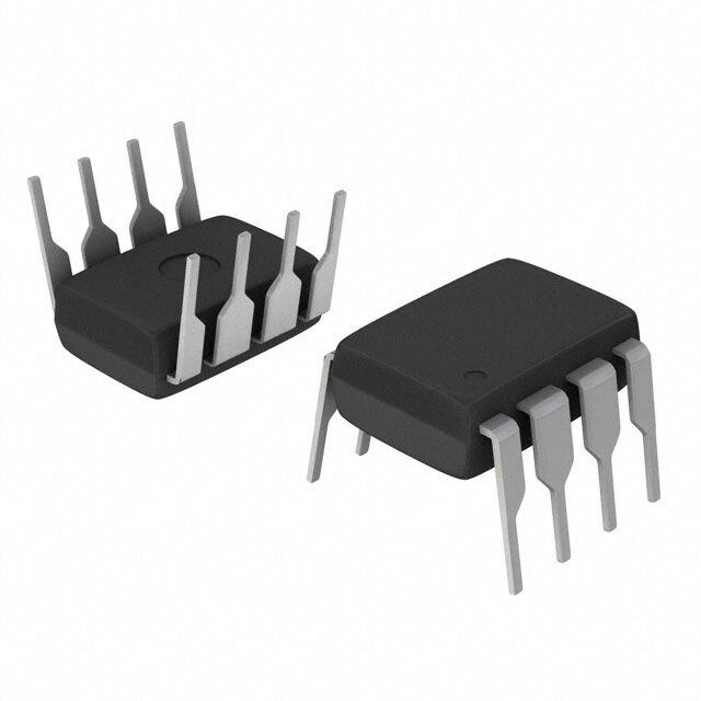
ICGOO电子元器件商城为您提供TLC555IP由Texas Instruments设计生产,在icgoo商城现货销售,并且可以通过原厂、代理商等渠道进行代购。 TLC555IP价格参考¥4.80-¥6.00。Texas InstrumentsTLC555IP封装/规格:时钟/计时 - 可编程计时器和振荡器, 555 Type, Timer/Oscillator (Single) IC 2.1MHz 8-PDIP。您可以下载TLC555IP参考资料、Datasheet数据手册功能说明书,资料中有TLC555IP 详细功能的应用电路图电压和使用方法及教程。
TLC555IP 是 Texas Instruments(德州仪器)推出的一款基于 555 定时器的集成电路,属于时钟/计时 - 可编程计时器和振荡器分类。它是一种多功能的模拟定时控制芯片,广泛应用于各种电子电路中,能够实现单稳态、多稳态及无稳态工作模式。以下是 TLC555IP 的主要应用场景:

1. 脉冲发生器
   TLC555IP 可用作脉冲信号生成器,产生精确的周期性脉冲信号。例如,在通信系统中用于数据同步或触发其他设备。

2. 振荡器电路
   在需要稳定振荡信号的场合,如音频信号发生器、蜂鸣器驱动等,TLC555IP 能够提供可调频率的方波输出。

3. 定时控制
   该芯片适用于需要精确时间延迟的场景,比如家用电器的延时开关功能、灯光定时控制器以及工业自动化中的定时任务管理。

4. PWM 控制
   TLC555IP 可配置为脉宽调制(PWM)控制器,用于调节电机速度、LED 亮度或电源电压转换等应用。

5. 触发电路
   在安防系统中,TLC555IP 可作为传感器触发后的延迟响应单元,例如运动检测后启动报警装置。

6. 电子玩具与教育实验
   因其简单易用且成本低廉,TLC555IP 常被用于开发电子玩具或作为教学工具,帮助学生理解基本电子电路原理。

7. 医疗设备辅助功能
   在某些便携式医疗设备中,可以利用 TLC555IP 实现间歇性信号输出,比如血压计的充气泵控制或脉搏监测提示音。

总之,TLC555IP 凭借其高可靠性和灵活性,成为众多电子产品设计中的重要组成部分,尤其适合对功耗要求不高但需要精准定时或振荡功能的应用领域。
| 参数 | 数值 |
| 产品目录 | 集成电路 (IC)半导体 |
| 描述 | IC OSC SINGLE TIMER 2.1MHZ 8-DIP计时器和支持产品 CMOS |
| 产品分类 | |
| 品牌 | Texas Instruments |
| 产品手册 | |
| 产品图片 |
|
| rohs | 符合RoHS无铅 / 符合限制有害物质指令(RoHS)规范要求 |
| 产品系列 | 时钟和计时器IC,计时器和支持产品,Texas Instruments TLC555IPLinCMOS™ |
| 数据手册 | |
| 产品型号 | TLC555IP |
| PCN设计/规格 | |
| 产品目录页面 | |
| 产品种类 | 计时器和支持产品 |
| 供应商器件封装 | 8-PDIP |
| 其它名称 | 296-1858 |
| 内部定时器数量 | 1 |
| 包装 | 管件 |
| 单位重量 | 440.400 mg |
| 商标 | Texas Instruments |
| 安装类型 | 通孔 |
| 安装风格 | Through Hole |
| 封装 | Tube |
| 封装/外壳 | 8-DIP(0.300",7.62mm) |
| 封装/箱体 | PDIP-8 |
| 工作温度 | -40°C ~ 85°C |
| 工厂包装数量 | 50 |
| 最大功率耗散 | 1000 mW |
| 最大工作温度 | + 85 C |
| 最小工作温度 | - 40 C |
| 标准包装 | 50 |
| 电压-电源 | 3 V ~ 15 V |
| 电流-电源 | 360µA |
| 电源电压-最大 | 15 V |
| 电源电压-最小 | 2 V |
| 电源电流 | 250 uA |
| 类型 | 555 型,计时器/振荡器(单路) |
| 系列 | TLC555 |
| 计数 | - |
| 频率 | 2.1MHz |


- 商务部:美国ITC正式对集成电路等产品启动337调查
- 曝三星4nm工艺存在良率问题 高通将骁龙8 Gen1或转产台积电
- 太阳诱电将投资9.5亿元在常州建新厂生产MLCC 预计2023年完工
- 英特尔发布欧洲新工厂建设计划 深化IDM 2.0 战略
- 台积电先进制程称霸业界 有大客户加持明年业绩稳了
- 达到5530亿美元!SIA预计今年全球半导体销售额将创下新高
- 英特尔拟将自动驾驶子公司Mobileye上市 估值或超500亿美元
- 三星加码芯片和SET,合并消费电子和移动部门,撤换高东真等 CEO
- 三星电子宣布重大人事变动 还合并消费电子和移动部门
- 海关总署:前11个月进口集成电路产品价值2.52万亿元 增长14.8%


PDF Datasheet 数据手册内容提取
Product Sample & Technical Tools & Support & Reference Folder Buy Documents Software Community Design TLC555 SLFS043H–SEPTEMBER1983–REVISEDAUGUST2016 TLC555 LinCMOS™ Timer 1 Features 3 Description • VeryLowPowerConsumption: The TLC555 is a monolithic timing circuit fabricated 1 using the TI LinCMOS™ process. The timer is fully – 1mWTypicalatV =5V DD compatible with CMOS, TTL, and MOS logic, and • CapableofOperationinAstableMode operates at frequencies up to 2 MHz. Because of its • CMOSOutputCapableofSwingingRailtoRail high input impedance, this device uses smaller timing capacitors than those used by the NE555. As a • HighOutputCurrentCapability result, more accurate time delays and oscillations are – Sink:100mATypical possible. Power consumption is low across the full – Source:10mATypical rangeofpower-supplyvoltage. • OutputFullyCompatibleWithCMOS,TTL,and Like the NE555, the TLC555 has a trigger level equal MOS toapproximatelyone-thirdofthesupplyvoltageanda • LowSupplyCurrentReducesSpikesDuring threshold level equal to approximately two-thirds of the supply voltage. These levels can be altered by OutputTransitions use of the control voltage terminal (CONT). When the • Single-SupplyOperationFrom2Vto15V trigger input (TRIG) falls below the trigger level, the • FunctionallyInterchangeableWiththeNE555; flip-flop is set and the output goes high. If TRIG is HasSamePinout above the trigger level and the threshold input • ESDProtectionExceeds2000VPerMIL-STD- (THRES) is above the threshold level, the flip-flop is reset and the output is low. The reset input (RESET) 883C,Method3015.2 can override all other inputs and can be used to • AvailableinQ-TempAutomotive initiate a new timing cycle. If RESET is low, the flip- – High-ReliabilityAutomotiveApplications flop is reset and the output is low. Whenever the – ConfigurationControlandPrintSupport output is low, a low-impedance path is provided between the discharge terminal (DISCH) and GND. – QualificationtoAutomotiveStandards All unused inputs must be tied to an appropriate logic leveltopreventfalsetriggering. 2 Applications • PrecisionTiming DeviceInformation(1) • PulseGeneration PARTNUMBER PACKAGE BODYSIZE(NOM) • SequentialTiming SOIC(8) 4.9mm×3.91mm PDIP(8) 9.81mm×6.38mm • TimeDelayGeneration TLC555C SOP(8) 6.20mm×5.30mm • PulseWidthModulation TSSOP(14) 5.00mm×4.40mm • PulsePositionModulation SOIC(8) 4.90mm×3.91mm • LinearRampGenerator TLC555I PDIP(8) 9.81mm×6.38mm SimplifiedSchematic LCCC(20) 8.89mm×8.89mm TLC555M CDIP(8) 9.60mm×6.67mm CONT RESET 5 4 TLC555Q SOIC(8) 4.90mm×3.91mm VDD 8 (1) For all available packages, see the orderable addendum at theendofthedatasheet. R 6 R1 THRES 3 R 1 OUT S R 2 TRIG R 7 DISCH 1 GND Copyright ' 2016, Texas Instruments Incorporated 1 An IMPORTANT NOTICE at the end of this data sheet addresses availability, warranty, changes, use in safety-critical applications, intellectualpropertymattersandotherimportantdisclaimers.PRODUCTIONDATA.
TLC555 SLFS043H–SEPTEMBER1983–REVISEDAUGUST2016 www.ti.com Table of Contents 1 Features.................................................................. 1 8.2 FunctionalBlockDiagram.......................................15 2 Applications........................................................... 1 8.3 FeatureDescription.................................................15 3 Description............................................................. 1 8.4 DeviceFunctionalModes........................................19 4 RevisionHistory..................................................... 2 9 ApplicationandImplementation........................ 20 9.1 ApplicationInformation............................................20 5 DeviceComparisonTable..................................... 3 9.2 TypicalApplications................................................20 6 PinConfigurationandFunctions......................... 3 10 PowerSupplyRecommendations..................... 26 7 Specifications......................................................... 6 11 Layout................................................................... 27 7.1 AbsoluteMaximumRatings......................................6 11.1 LayoutGuidelines.................................................27 7.2 RecommendedOperatingConditions.......................6 11.2 LayoutExample....................................................27 7.3 ThermalInformation..................................................6 12 DeviceandDocumentationSupport................. 28 7.4 ElectricalCharacteristics:V =2VforTLC555C, DD V =3VforTLC555I...............................................7 12.1 ReceivingNotificationofDocumentationUpdates28 DD 7.5 ElectricalCharacteristics:V =5V.........................8 12.2 CommunityResources..........................................28 DD 7.6 ElectricalCharacteristics:V =15V.....................11 12.3 Trademarks...........................................................28 DD 7.7 ElectricalCharacteristics:V =5V......................14 12.4 ElectrostaticDischargeCaution............................28 DD 7.8 TypicalCharacteristics............................................14 12.5 Glossary................................................................28 8 DetailedDescription............................................ 15 13 Mechanical,Packaging,andOrderable 8.1 Overview.................................................................15 Information........................................................... 28 4 Revision History ChangesfromRevisionG(November2008)toRevisionH Page • AddedFeatureDescriptionsection,DeviceFunctionalModes,ApplicationandImplementationsection,Power SupplyRecommendationssection,Layoutsection,DeviceandDocumentationSupportsection,andMechanical, Packaging,andOrderableInformationsection ..................................................................................................................... 1 • DeletedContinuoustotalpowerdissipationandleadtemperatureparametersfromAbsoluteMaximumRatings............... 6 • ChangedvaluesintheThermalInformationtabletoalignwithJEDECstandards................................................................ 6 • DeletedDissipationRatingstable.......................................................................................................................................... 6 2 SubmitDocumentationFeedback Copyright©1983–2016,TexasInstrumentsIncorporated ProductFolderLinks:TLC555
TLC555 www.ti.com SLFS043H–SEPTEMBER1983–REVISEDAUGUST2016 5 Device Comparison Table SMALL CHIP CERAMIC PLASTIC V SSOP TSSOP DEVICE T DD OUTLINE CARRIER DIP DIP A RANGE (PS) (PW) (D) (FK) (JG) (P) TLC555C 0°Cto70°C 2Vto15V ✓ — — ✓ ✓ ✓ TLC555I –40°Cto85°C 3Vto15V ✓ — — ✓ — — TLC555M –55°Cto125°C 5Vto15V — ✓ ✓ — — — TLC555Q –40°Cto125°C 5Vto15V ✓ — — — — — 6 Pin Configuration and Functions TLC555C:D,P,andPSPackages TLC555C:PWPackage 8-PinSOIC,PDIP,SOP 14-PinTSSOP TopView TopView GND 1 8 VDD GND 1 14 VDD TRIG 2 7 DISCH NC 2 13 NC OUT 3 6 THRES RESET 4 5 CONT TRIG 3 12 DISCH NC 4 11 NC OUT 5 10 THRES NC 6 9 NC RESET 7 8 CONT PinFunctions:TLC555C PIN SOIC, I/O DESCRIPTION NAME PDIP, TSSOP SOP Controlscomparatorthresholds.Outputs2/3V andallowsbypasscapacitor CONT 5 8 I DD connection. DISCH 7 12 O Opencollectoroutputtodischargetimingcapacitor GND 1 1 Ground 2,4,6, NC — — Nointernalconnection 9,11,13 OUT 3 5 O Highcurrenttimeroutputsignal RESET 4 7 I Activelowresetinputforcesoutputanddischargelow THRES 6 10 I Endoftiminginput.THRES>CONTsetsoutputlowanddischargelow. TRIG 2 3 I Startoftiminginput.TRIG<½CONTsetsoutputhighanddischargeopen. V 8 14 — Power-supplyvoltage DD Copyright©1983–2016,TexasInstrumentsIncorporated SubmitDocumentationFeedback 3 ProductFolderLinks:TLC555
TLC555 SLFS043H–SEPTEMBER1983–REVISEDAUGUST2016 www.ti.com TLC555I:DandPPackages 8-PinSOIC,PDIP TopView GND 1 8 V DD TRIG 2 7 DISCH OUT 3 6 THRES RESET 4 5 CONT PinFunctions:TLC555I PIN I/O DESCRIPTION NAME SOIC,PDIP CONT 5 I Controlscomparatorthresholds.Outputs2/3V andallowsbypasscapacitorconnection. DD DISCH 7 O Open-collectoroutputtodischargetimingcapacitor GND 1 — Ground OUT 3 O Highcurrenttimeroutputsignal RESET 4 I Activelowresetinputforcesoutputanddischargelow THRES 6 I Endoftiminginput.THRES>CONTsetsoutputlowanddischargelow. TRIG 2 I Startoftiminginput.TRIG<½CONTsetsoutputhighanddischargeopen. V 8 — Power-supplyvoltage DD 4 SubmitDocumentationFeedback Copyright©1983–2016,TexasInstrumentsIncorporated ProductFolderLinks:TLC555
TLC555 www.ti.com SLFS043H–SEPTEMBER1983–REVISEDAUGUST2016 TLC555M:JGPackage TLC555M:FKPackage 8-PinCDIP 20-PinLCCC TopView TopView GND 1 8 VDD NC GND NC VDD NC TRIG 2 7 DISCH 3 2 1 20 19 OUT 3 6 THRES NC 4 18 NC RESET 4 5 CONT TRIG 5 17 DISCH NC 6 16 NC OUT 7 15 THRES NC 8 14 NC 9 10 11 12 13 C T C T C N E N N N S O RE C PinFunctions:TLC555M PIN I/O DESCRIPTION NAME LCCC CDIP CONT 12 5 I Controlscomparatorthresholds.Outputs2/3VDDandallowsbypasscapacitorconnection. DISCH 17 7 O Open-collectoroutputtodischargetimingcapacitor GND 2 1 — Ground 1,3,4,6,8, NC 9,11,13,14, — — Nointernalconnection 16,18,19 OUT 7 3 O Highcurrenttimeroutputsignal RESET 10 4 I Activelowresetinputforcesoutputanddischargelow THRES 15 6 I Endoftiminginput.THRES>CONTsetsoutputlowanddischargelow. TRIG 5 2 I Startoftiminginput.TRIG<½CONTsetsoutputhighanddischargeopen. VDD 20 8 — Power-supplyvoltage TLC555Q:DPackage 8-PinSOIC TopView GND 1 8 V DD TRIG 2 7 DISCH OUT 3 6 THRES RESET 4 5 CONT PinFunctions:TLC555Q PIN I/O DESCRIPTION NAME SOIC CONT 5 I Controlscomparatorthresholds,Outputs2/3VDD,allowsbypasscapacitorconnection DISCH 7 O Open-collectoroutputtodischargetimingcapacitor GND 1 — Ground OUT 3 O Highcurrenttimeroutputsignal RESET 4 I Activelowresetinputforcesoutputanddischargelow THRES 6 I Endoftiminginput.THRES>CONTsetsoutputlowanddischargelow TRIG 2 I Startoftiminginput.TRIG<½CONTsetsoutputhighanddischargeopen VDD 8 — Powersupplyvoltage Copyright©1983–2016,TexasInstrumentsIncorporated SubmitDocumentationFeedback 5 ProductFolderLinks:TLC555
TLC555 SLFS043H–SEPTEMBER1983–REVISEDAUGUST2016 www.ti.com 7 Specifications 7.1 Absolute Maximum Ratings overoperatingfree-airtemperaturerange(unlessotherwisenoted)(1) MIN MAX UNIT Supply,V (2) 18 V DD Voltage Input,anyinput −0.3 V V DD Sink,dischargeoroutput 150 mA Current Source,output,I 15 mA O C-suffix 0 70 °C I-suffix –40 85 °C Operating,T A Q-suffix –40 125 °C Temperature M-suffix –55 125 °C Case,for60seconds FKpackage –65 150 °C Storage,T –65 150 °C stg (1) StressesbeyondthoselistedunderAbsoluteMaximumRatingsmaycausepermanentdamagetothedevice.Thesearestressratings only,whichdonotimplyfunctionaloperationofthedeviceattheseoranyotherconditionsbeyondthoseindicatedunderRecommended OperatingConditions.Exposuretoabsolute-maximum-ratedconditionsforextendedperiodsmayaffectdevicereliability. (2) AllvoltagevaluesarewithrespecttonetworkGND. 7.2 Recommended Operating Conditions overoperatingfree-airtemperaturerange(unlessotherwisenoted) MIN MAX UNIT Supplyvoltage,V 2 15 V DD TLC555C 0 70 °C Operatingfree-air TLC555I –40 85 °C temperature,TA TLC555M –55 125 °C TLC555Q –40 125 °C 7.3 Thermal Information TLC555 THERMALMETRIC(1) D FK JG P PS PW UNIT (SOIC) (LCCC) (CDIP) (PDIP) (SOP) (TSSOP) 8PINS 20PINS 8PINS 8PINS 8PINS 14PINS R Junction-to-ambientthermalresistance 113 n/a 120 58 120 135 °C/W θJA R Junction-to-case(top)thermalresistance 58 37 81 48 72 61 °C/W θJC(top) R Junction-to-boardthermalresistance 55 36 110 35 69 77 °C/W θJB Junction-to-topcharacterization ψ 11 n/a 45 26 32 12 °C/W JT parameter Junction-to-boardcharacterization ψ 54 n/a 103 35 68 77 °C/W JB parameter Junction-to-case(bottom)thermal R n/a 4.3 31 n/a n/a n/a °C/W θJC(bot) resistance (1) Formoreinformationabouttraditionalandnewthermalmetrics,seetheSemiconductorandICPackageThermalMetricsapplication report. 6 SubmitDocumentationFeedback Copyright©1983–2016,TexasInstrumentsIncorporated ProductFolderLinks:TLC555
TLC555 www.ti.com SLFS043H–SEPTEMBER1983–REVISEDAUGUST2016 7.4 Electrical Characteristics: V = 2 V for TLC555C, V = 3 V for TLC555I DD DD overoperatingfree-airtemperaturerange(unlessotherwisenoted) PARAMETER TESTCONDITIONS(1) MIN TYP MAX UNIT TLC555C 0.95 1.33 1.65 25°C V TLC555I 1.6 2.4 VIT Thresholdvoltage TLC555C 0.85 1.75 Fullrange V TLC555I 1.5 2.5 TLC555C 10 25°C pA TLC555I 10 IIT Thresholdcurrent TLC555C 75 Max pA TLC555I 150 TLC555C 0.4 0.67 0.95 25°C V TLC555I 0.71 1 1.29 VI(TRIG) Triggervoltage TLC555C 0.3 1.05 Fullrange V TLC555I 0.61 1.39 TLC555C 10 25°C pA TLC555I 10 II(TRIG) Triggercurrent TLC555C 75 Max pA TLC555I 150 TLC555C 0.4 1.1 1.5 25°C V TLC555I 0.4 1.1 1.5 VI(RESET) Resetvoltage TLC555C 0.3 2 Fullrange V TLC555I 0.3 1.8 Controlvoltage(open-circuit)asa TLC555C 66.7% Max percentageofsupplyvoltage TLC555I 66.7% TLC555C 0.03 0.2 IOL=1mA,25°C V Dischargeswitchon-stage TLC555I 0.03 0.2 voltage TLC555C 0.25 IOL=1mA,Fullrange V TLC555I 0.375 TLC555C 0.1 25°C nA Dischargeswitchoff-stage TLC555I 0.1 current TLC555C 0.5 Max nA TLC555I 120 TLC555C 1.5 1.9 IOH=–300µA,25°C V TLC555I 2.5 2.85 VOH High-leveloutputvoltage IOH=–300µA, TLC555C 1.5 V Fullrange TLC555I 2.5 TLC555C 0.07 0.3 IOL=1mA,25°C V TLC555I 0.07 0.3 VOL Low-leveloutputvoltage TLC555C 0.35 IOL=1mA,Fullrange V TLC555I 0.4 TLC555C 250 25°C µA TLC555I 250 IDD Supplycurrent(2) TLC555C 400 Fullrange µA TLC555I 500 (1) Fullrangeis0°Cto70°CtheforTLC555C,and−40°Cto85°CfortheTLC555I.ForconditionsshownasMax,usetheappropriate valuespecifiedintheRecommendedOperatingConditionstable. (2) ThesevaluesapplyfortheexpectedoperatingconfigurationsinwhichTHRESisconnecteddirectlytoDISCHortoTRIG. Copyright©1983–2016,TexasInstrumentsIncorporated SubmitDocumentationFeedback 7 ProductFolderLinks:TLC555
TLC555 SLFS043H–SEPTEMBER1983–REVISEDAUGUST2016 www.ti.com 7.5 Electrical Characteristics: V = 5 V DD overoperatingfree-airtemperaturerange(unlessotherwisenoted) PARAMETER TESTCONDITIONS(1) MIN TYP MAX UNIT TLC555C 2.8 3.3 3.8 TLC555I 2.8 3.3 3.8 25°C V TLC555M 2.8 3.3 3.8 TLC555Q 2.8 3.3 3.8 VIT Thresholdvoltage TLC555C 2.7 3.9 TLC555I 2.7 3.9 Fullrange V TLC555M 2.7 3.9 TLC555Q 2.7 3.9 TLC555C 10 TLC555I 10 25°C pA TLC555M 10 TLC555Q 10 IIT Thresholdcurrent TLC555C 75 TLC555I 150 Max pA TLC555M 5000 TLC555Q 5000 TLC555C 1.36 1.66 1.96 TLC555I 1.36 1.66 1.96 25°C V TLC555M 1.36 1.66 1.96 TLC555Q 1.36 1.66 1.96 VI(TRIG) Triggervoltage TLC555C 1.26 2.06 TLC555I 1.26 2.06 Fullrange V TLC555M 1.26 2.06 TLC555Q 1.26 2.06 TLC555C 10 TLC555I 10 25°C pA TLC555M 10 TLC555Q 10 II(TRIG) Triggercurrent TLC555C 75 TLC555I 150 Max pA TLC555M 5000 TLC555Q 5000 TLC555C 0.4 1.1 1.5 TLC555I 0.4 1.1 1.5 25°C V TLC555M 0.4 1.1 1.5 TLC555Q 0.4 1.1 1.5 VI(RESET) Resetvoltage TLC555C 0.3 1.8 TLC555I 0.3 1.8 Fullrange V TLC555M 0.3 1.8 TLC555Q 0.3 1.8 TLC555C 10 TLC555I 10 25°C pA TLC555M 10 TLC555Q 10 II(RESET) Resetcurrent TLC555C 75 TLC555I 150 Max pA TLC555M 5000 TLC555Q 5000 (1) Fullrangeis0°Cto70°CtheforTLC555C,−40°Cto85°CfortheTLC555I,−40°Cto125°CfortheTLC555Q,and−55°Cto125°Cfor theTLC555M.ForconditionsshownasMax,usetheappropriatevaluespecifiedintheRecommendedOperatingConditionstable. 8 SubmitDocumentationFeedback Copyright©1983–2016,TexasInstrumentsIncorporated ProductFolderLinks:TLC555
TLC555 www.ti.com SLFS043H–SEPTEMBER1983–REVISEDAUGUST2016 Electrical Characteristics: V = 5 V (continued) DD overoperatingfree-airtemperaturerange(unlessotherwisenoted) PARAMETER TESTCONDITIONS(1) MIN TYP MAX UNIT TLC555C 66.7% Controlvoltage(opencircuit)asa TLC555I 66.7% Max percentageofsupplyvoltage TLC555M 66.7% TLC555Q 66.7% TLC555C 0.14 0.5 TLC555I 0.14 0.5 IOL=10mA,25°C V TLC555M 0.14 0.5 Dischargeswitchon-stage TLC555Q 0.14 0.5 voltage TLC555C 0.6 IOL=10mA, TLC555I 0.6 V Fullrange TLC555M 0.6 TLC555Q 0.6 TLC555C 0.1 TLC555I 0.1 25°C nA TLC555M 0.1 Dischargeswitchoff-stage TLC555Q 0.1 current TLC555C 0.5 TLC555I 120 Max nA TLC555M 120 TLC555Q 120 TLC555C 4.1 4.8 TLC555I 4.1 4.8 IOH=–1µA,25°C V TLC555M 4.1 4.8 TLC555Q 4.1 4.8 VOH High-leveloutputvoltage TLC555C 4.1 IOH=–1µA, TLC555I 4.1 V Fullrange TLC555M 4.1 TLC555Q 4.1 TLC555C 0.21 0.4 TLC555I 0.21 0.4 IOL=8mA,25°C V TLC555M 0.21 0.4 TLC555Q 0.21 0.4 VOL Low-leveloutputvoltage TLC555C 0.5 IOL=8mA, TLC555I 0.5 V Fullrange TLC555M 0.6 TLC555Q 0.6 Copyright©1983–2016,TexasInstrumentsIncorporated SubmitDocumentationFeedback 9 ProductFolderLinks:TLC555
TLC555 SLFS043H–SEPTEMBER1983–REVISEDAUGUST2016 www.ti.com Electrical Characteristics: V = 5 V (continued) DD overoperatingfree-airtemperaturerange(unlessotherwisenoted) PARAMETER TESTCONDITIONS(1) MIN TYP MAX UNIT TLC555C 0.13 0.3 TLC555I 0.13 0.3 IOL=5mA,25°C V TLC555M 0.13 0.3 TLC555Q 0.13 0.3 TLC555C 0.4 IOL=5mA, TLC555I 0.4 V Fullrange TLC555M 0.45 TLC555Q 0.45 VOL Low-leveloutputvoltage TLC555C 0.08 0.3 TLC555I 0.08 0.3 IOL=3.2mA,25°C V TLC555M 0.8 0.3 TLC555Q 0.8 0.3 TLC555C 0.35 IOL=3.2mA, TLC555I 0.35 V Fullrange TLC555M 0.4 TLC555Q 0.4 TLC555C 170 350 TLC555I 170 350 25°C µA TLC555M 170 350 TLC555Q 170 350 IDD Supplycurrent(2) TLC555C 500 TLC555I 600 Fullrange µA TLC555M 700 TLC555Q 700 (2) ThesevaluesapplyfortheexpectedoperatingconfigurationsinwhichTHRESisconnecteddirectlytoDISCHortoTRIG. 10 SubmitDocumentationFeedback Copyright©1983–2016,TexasInstrumentsIncorporated ProductFolderLinks:TLC555
TLC555 www.ti.com SLFS043H–SEPTEMBER1983–REVISEDAUGUST2016 7.6 Electrical Characteristics: V = 15 V DD overoperatingfree-airtemperaturerange(unlessotherwisenoted) PARAMETER TESTCONDITIONS(1) MIN TYP MAX UNIT TLC555C 9.45 10 10.55 TLC555I 9.45 10 10.55 25°C V TLC555M 9.45 10 10.55 TLC555Q 9.45 10 10.55 VIT Thresholdvoltage TLC555C 9.35 10.65 TLC555I 9.35 10.65 Fullrange V TLC555M 9.35 10.65 TLC555Q 9.35 10.65 TLC555C 10 TLC555I 10 25°C pA TLC555M 10 TLC555Q 10 IIT Thresholdcurrent TLC555C 75 TLC555I 150 Max pA TLC555M 5000 TLC555Q 5000 TLC555C 4.65 5 5.35 TLC555I 4.65 5 5.35 25°C V TLC555M 4.65 5 5.35 TLC555Q 4.65 5 5.35 VI(TRIG) Triggervoltage TLC555C 4.55 5.45 TLC555I 4.55 5.45 Fullrange V TLC555M 4.55 5.45 TLC555Q 4.55 5.45 TLC555C 10 TLC555I 10 25°C pA TLC555M 10 TLC555Q 10 II(TRIG) Triggercurrent TLC555C 75 TLC555I 150 Max pA TLC555M 5000 TLC555Q 5000 TLC555C 0.4 1.1 1.5 TLC555I 0.4 1.1 1.5 25°C V TLC555M 0.4 1.1 1.5 TLC555Q 0.4 1.1 1.5 VI(RESET) Resetvoltage TLC555C 0.3 1.8 TLC555I 0.3 1.8 Fullrange V TLC555M 0.3 1.8 TLC555Q 0.3 1.8 TLC555C 10 TLC555I 10 25°C pA TLC555M 10 TLC555Q 10 II(RESET) Resetcurrent TLC555C 75 TLC555I 150 Max pA TLC555M 5000 TLC555Q 5000 (1) Fullrangeis0°Cto70°CforTLC555C,−40°Cto85°CforTLC555I,−40°Cto125°CfortheTLC555Q,and−55°Cto125°Cfor TLC555M.ForconditionsshownasMax,usetheappropriatevaluespecifiedintheRecommendedOperatingConditionstable. Copyright©1983–2016,TexasInstrumentsIncorporated SubmitDocumentationFeedback 11 ProductFolderLinks:TLC555
TLC555 SLFS043H–SEPTEMBER1983–REVISEDAUGUST2016 www.ti.com Electrical Characteristics: V = 15 V (continued) DD overoperatingfree-airtemperaturerange(unlessotherwisenoted) PARAMETER TESTCONDITIONS(1) MIN TYP MAX UNIT TLC555C 66.7% Controlvoltage(opencircuit)asa TLC555I 66.7% Max percentageofsupplyvoltage TLC555M 66.7% TLC555Q 66.7% TLC555C 0.77 1.7 TLC555I 0.77 1.7 IOL=100mA,25°C V TLC555M 0.77 1.7 Dischargeswitchon-stage TLC555Q 0.77 1.7 voltage TLC555C 1.8 IOL=100mA, TLC555I 1.8 V Fullrange TLC555M 1.8 TLC555Q 1.8 TLC555C 0.1 TLC555I 0.1 25°C nA TLC555M 0.1 Dischargeswitchoff-stage TLC555Q 0.1 current TLC555C 0.5 TLC555I 120 Max nA TLC555M 120 TLC555Q 120 TLC555C 12.5 14.2 TLC555I 12.5 14.2 IOH=–10mA,25°C V TLC555M 12.5 14.2 TLC555Q 12.5 14.2 TLC555C 12.5 IOH=–10mA, TLC555I 12.5 V Fullrange TLC555M 12.5 TLC555Q 12.5 TLC555C 13.5 14.6 TLC555I 13.5 14.6 IOH=–5mA,25°C V TLC555M 13.5 14.6 TLC555Q 13.5 14.6 VOH High-leveloutputvoltage TLC555C 13.5 IOH=–5mA, TLC555I 13.5 V Fullrange TLC555M 13.5 TLC555Q 13.5 TLC555C 14.2 14.9 TLC555I 14.2 14.9 IOH=–1mA,25°C V TLC555M 14.2 14.9 TLC555Q 14.2 14.9 TLC555C 14.2 IOH=–1mA, TLC555I 14.2 V Fullrange TLC555M 14.2 TLC555Q 14.2 12 SubmitDocumentationFeedback Copyright©1983–2016,TexasInstrumentsIncorporated ProductFolderLinks:TLC555
TLC555 www.ti.com SLFS043H–SEPTEMBER1983–REVISEDAUGUST2016 Electrical Characteristics: V = 15 V (continued) DD overoperatingfree-airtemperaturerange(unlessotherwisenoted) PARAMETER TESTCONDITIONS(1) MIN TYP MAX UNIT TLC555C 1.28 3.2 TLC555I 1.28 3.2 IOL=100mA,25°C V TLC555M 1.28 3.2 TLC555Q 1.28 3.2 TLC555C 3.6 IOL=100mA, TLC555I 3.7 V Fullrange TLC555M 3.8 TLC555Q 3.8 TLC555C 0.63 1 TLC555I 0.63 1 IOL=50mA,25°C V TLC555M 0.63 1 TLC555Q 0.63 1 VOL Low-leveloutputvoltage TLC555C 1.3 IOL=50mA, TLC555I 1.4 V Fullrange TLC555M 1.5 TLC555Q 1.5 TLC555C 0.12 0.3 TLC555I 0.12 0.3 IOL=10mA,25°C V TLC555M 0.12 0.3 TLC555Q 0.12 0.3 TLC555C 0.4 IOL=10mA, TLC555I 0.4 V Fullrange TLC555M 0.45 TLC555Q 0.45 TLC555C 360 600 TLC555I 360 600 25°C µA TLC555M 360 600 TLC555Q 360 600 IDD Supplycurrent(2) TLC555C 800 TLC555I 900 Fullrange µA TLC555M 1000 TLC555Q 1000 (2) ThesevaluesapplyfortheexpectedoperatingconfigurationsinwhichTHRESisconnecteddirectlytoDISCHorTRIG. Copyright©1983–2016,TexasInstrumentsIncorporated SubmitDocumentationFeedback 13 ProductFolderLinks:TLC555
TLC555 SLFS043H–SEPTEMBER1983–REVISEDAUGUST2016 www.ti.com 7.7 Electrical Characteristics: V = 5 V DD AtT =25°C,overoperatingfree-airtemperaturerange(unlessotherwisenoted) A PARAMETER TESTCONDITIONS MIN TYP MAX UNIT V Thresholdvoltage 2.8 3.3 3.8 V IT I Thresholdcurrent 10 pA IT V Triggervoltage 1.36 1.66 1.96 V I(TRIG) I Triggercurrent 10 pA I(TRIG) V Resetvoltage 0.4 1.1 1.5 V I(RESET) I Resetcurrent 10 pA I(RESET) Controlvoltage(opencircuit)asa 66.7% percentageofsupplyvoltage Dischargeswitchon-stagevoltage I =10mA 0.14 0.5 v OL Dischargeswitchoff-stagecurrent 0.1 nA V High-leveloutputvoltage I =–1mA 4.1 4.8 V OH OH I =8mA 0.21 0.4 V OL V Low-leveloutputvoltage I =5mA 0.13 0.3 V OL OL I =3.2mA 0.08 0.3 V OL I Supplycurrent(1) 170 350 µA DD (1) ThesevaluesapplyfortheexpectedoperatingconfigurationsinwhichTHRESisconnecteddirectlytoDISCHorTRIG. 7.8 Typical Characteristics W) 100 600 e Resistance ( 247000 VDD= 2V VDD, I=O 5= V1, mIOA= 10 mA Times (ns) 540000 ICTOAL(o=»n) 02³5°1C mA at y n-St 10 Dela 300 h O 7 VDD= 15 V, IO= 100 mA on tPHL witc 4 gati 200 e S opa scharg 2 Pr 100 tPLH(1) Di 1 0 -75 -50 -25 0 25 50 75 100 125 0 2 4 6 8 10 12 14 16 18 20 Temperature (°C) Supply Voltage (V) (1)Theeffectsoftheloadresistanceonthesevaluesmustbe takenintoaccountseparately. Figure1.DischargeSwitchON-StateResistancevs Figure2.PropagationDelayTimestoDischargeOutput fromTriggerandThresholdShortedTogether Free-AirTemperature vsSupplyVoltage 14 SubmitDocumentationFeedback Copyright©1983–2016,TexasInstrumentsIncorporated ProductFolderLinks:TLC555
TLC555 www.ti.com SLFS043H–SEPTEMBER1983–REVISEDAUGUST2016 8 Detailed Description 8.1 Overview TheTLC555isaprecisiontimingdeviceusedforgeneral-purposetimingapplicationsupto2.1MHz. 8.2 Functional Block Diagram CONT RESET 5 4 VDD 8 R R1 6 THRES 3 R 1 OUT S R 2 TRIG R 7 DISCH 1 GND Copyright ' 2016, Texas Instruments Incorporated PinnumbersareforallpackagesexcepttheFKpackage.RESETcanoverrideTRIG,whichcanoverrideTHRES. 8.3 Feature Description 8.3.1 MonostableOperation For monostable operation, any of these timers can be connected as shown in Figure 3. If the output is low, application of a negative-going pulse to the trigger (TRIG) sets the flip-flop (Q goes low), drives the output high, and turns off Q1. Capacitor C then is charged through R until the voltage across the capacitor reaches the A thresholdvoltageofthethreshold(THRES)input.IfTRIGhasreturnedtoahighlevel,theoutputofthethreshold comparatorresetstheflip-flop(Qgoeshigh),drivestheoutputlow,anddischargesCthroughQ1. Copyright©1983–2016,TexasInstrumentsIncorporated SubmitDocumentationFeedback 15 ProductFolderLinks:TLC555
TLC555 SLFS043H–SEPTEMBER1983–REVISEDAUGUST2016 www.ti.com Feature Description (continued) VDD (5 V to 15 V) RA 5 8 CONT VDD RL 4 RESET 7 DISCH 3 OUT Output 6 THRES 2 Input TRIG GND 1 Copyright © 2016, Texas Instruments Incorporated Figure3. CircuitforMonostableOperation Monostable operation is initiated when TRIG voltage falls below the trigger threshold. Once initiated, the sequence ends only if TRIG is high for at least 10 µs before the end of the timing interval. When the trigger is grounded, the comparator storage time can be as long as 10 µs, which limits the minimum monostable pulse width to 10 µs. Because of the threshold level and saturation voltage of Q1, the output pulse duration is approximately t = 1.1R C. Figure 4 is a plot of the time constant for various values of R and C. The threshold w A A levels and charge rates both are directly proportional to the supply voltage, V . The timing interval is, therefore, CC independentofthesupplyvoltage,solongasthesupplyvoltageisconstantduringthetimeinterval. Applying a negative-going trigger pulse simultaneously to RESET and TRIG during the timing interval discharges C and reinitiates the cycle, commencing on the positive edge of the reset pulse. The output is held low as long astheresetpulseislow.Topreventfalsetriggering,whenRESETisnotuseditmustbeconnectedtoV . CC 10 RA= 9.1 kW RA= 10 MW CL(cid:3)= 0.01(cid:3)mF RL= 1 kW See Figure 9 1 RA= 1 MW s − 10−1 n o v Input Voltage ati di ur V/ D 10−2 2 e s − ul e P Voltag utput 10−3 RA= 100 kW O Output Voltage −w 10−4 RA= 10 kW t RA= 1 kW Capacitor Voltage 10−5 0.001 0.01 0.1 1 10 100 Time−0.1 ms/div C−Capacitance−mF Figure4.TypicalMonostableWaveforms Figure5.OutputPulseDurationvsCapacitance 16 SubmitDocumentationFeedback Copyright©1983–2016,TexasInstrumentsIncorporated ProductFolderLinks:TLC555
TLC555 www.ti.com SLFS043H–SEPTEMBER1983–REVISEDAUGUST2016 Feature Description (continued) 8.3.2 AstableOperation As shown in Figure 6, adding a second resistor, R , to the circuit of Figure 3 and connecting the trigger input to B the threshold input causes the timer to self-trigger and run as a multi-vibrator. The capacitor C charges through R and R and then discharges through R only. Therefore, the duty cycle is controlled by the values of R and A B B A R . B This astable connection results in capacitor C charging and discharging between the threshold-voltage level (≈ 0.67 × V ) and the trigger-voltage level (≈ 0.33 × V ). As in the monostable circuit, charge and discharge CC CC times(and,therefore,thefrequencyanddutycycle)areindependentofthesupplyvoltage. DecouplingCONTvoltagetogroundwithacapacitorcanimproveoperation.Thisshouldbeevaluatedforindividual applications. (5 V VtoD D15 V) RA= 5 kW RL= 1 kW RB= 3 kW See Figure 12 C = 0.15mF 0.01PF Open RA (see NoteA) 5 8 div 4 CONT VDD RL 1 V/ RESET − 7 DISCH 3 ge a RB 6 THRES OUT Output Volt 2 TRIG tH GND C 1 tL Output Voltage NOTEA: DecouplingCONTvoltagetogroundwithacapacitorcan improveoperation.Thisshouldbeevaluatedforindividual Capacitor Voltage applications. Copyright © 2016, Texas Instruments Incorporated Time−0.5 ms/div Figure6.CircuitforAstableOperation Figure7.TypicalAstableWaveforms tc(L) tc(H) VDD tPHL 2/3 VDD 1/3 VDD GND tPLH Figure8.TriggerandThresholdVoltageWaveform Figure 7 shows typical waveforms generated during astable operation. The output high-level duration t and low- H leveldurationt canbecalculatedasfollows: L t =0.693(R +R )C H A B (1) t =0.693(R )C L B (2) Otherusefulrelationshipsareshownbelow: period=t +t =0.693(R +2R )C H L A B (3) Copyright©1983–2016,TexasInstrumentsIncorporated SubmitDocumentationFeedback 17 ProductFolderLinks:TLC555
TLC555 SLFS043H–SEPTEMBER1983–REVISEDAUGUST2016 www.ti.com Feature Description (continued) 1.44 frequency» (R +2R )C A B (4) t R Outputdriver dutycycle= L = B t +t R +2R H L A B (5) t R Outputwaveform dutycycle= H =1- B t +t R +2R H L A B (6) t R Low-to-highratio= L = B t R +R H A B (7) 100 k RA+ 2 RB= 1 kW RA+ 2 RB= 10 kW z 10 k −H RA+ 2 RB= 100 kW y c en 1 k u q e Fr ng 100 ni n u R e- 10 e Fr − f 1 RA+ 2 RB= 1 MW RA+ 2 RB= 10 MW 0.1 0.001 0.01 0.1 1 10 100 C−Capacitance−mF Figure9. Free-RunningFrequency 8.3.3 FrequencyDivider By adjusting the length of the timing cycle, the basic circuit of Figure 6 can be made to operate as a frequency divider. Figure 10 shows a divide-by-three circuit that makes use of the fact that re-triggering cannot occur during thetimingcycle. VCC= 5 V RA= 1250W C = 0.02mF See Figure 9 v V/di Input Voltage 2 − e g a olt V Output Voltage Capacitor Voltage Time−0.1 ms/div Figure10. Divide-by-ThreeCircuitWaveforms 18 SubmitDocumentationFeedback Copyright©1983–2016,TexasInstrumentsIncorporated ProductFolderLinks:TLC555
TLC555 www.ti.com SLFS043H–SEPTEMBER1983–REVISEDAUGUST2016 8.4 Device Functional Modes Table1showsthedevicefunctionalmodes. Table1.FunctionTable VORLETSAEGTE(1) TRIGGERVOLTAGE(1) TVHORLETSAHGOEL(1D) OUTPUT DISCHARGESWITCH <MIN Irrelevant Irrelevant L On >MAX <MIN Irrelevant H Off >MAX >MAX >MAX L On >MAX >MAX <MIN Aspreviouslyestablished (1) ForconditionsshownasMINorMAX,usetheappropriatevaluespecifiedunderElectricalCharacteristics:V =5V. DD COMPONENT COUNT Transistors 39 Resistors 5 THRES V DD CONT OUT DISCH GND TRIG RESET Copyright © 2016, Texas Instruments Incorporated Figure11. EquivalentSchematic(EachChannel) Copyright©1983–2016,TexasInstrumentsIncorporated SubmitDocumentationFeedback 19 ProductFolderLinks:TLC555
TLC555 SLFS043H–SEPTEMBER1983–REVISEDAUGUST2016 www.ti.com 9 Application and Implementation NOTE Information in the following applications sections is not part of the TI component specification, and TI does not warrant its accuracy or completeness. TI’s customers are responsible for determining suitability of components for their purposes. Customers should validateandtesttheirdesignimplementationtoconfirmsystemfunctionality. 9.1 Application Information The TLC555 timer device uses resistor and capacitor charging delay to provide a programmable time delay or operatingfrequency.TheTypicalApplicationssectionpresentsasimplifieddiscussionofthedesignprocess. 9.2 Typical Applications 9.2.1 Missing-PulseDetector The circuit shown in Figure 12 can be used to detect a missing pulse or abnormally long spacing between consecutive pulses in a train of pulses. The timing interval of the monostable circuit is re-triggered continuously by the input pulse train as long as the pulse spacing is less than the timing interval. A longer pulse spacing, missing pulse, or terminated pulse train permits the timing interval to be completed, thereby generating an output pulseasshowninFigure13. VDD(5 V to 15 V) 4 8 RL RA Input RESET VDD 3 OUT Output 2 TRIG 7 DISCH 5 CONT 6 0.01PF THRES GND C 1 A5T3644 Copyright © 2016, Texas Instruments Incorporated Figure12. CircuitforMissing-PulseDetector 9.2.1.1 DesignRequirements Input fault (missing pulses) must be input high. An input stuck low cannot be detected because the timing capacitor(C)remainsdischarged. 9.2.1.2 DetailedDesignProcedure Choose R and C so that R × C > [maximum normal input high time]. R improves V , but it is not required for A A L OH TTLcompatibility. 20 SubmitDocumentationFeedback Copyright©1983–2016,TexasInstrumentsIncorporated ProductFolderLinks:TLC555
TLC555 www.ti.com SLFS043H–SEPTEMBER1983–REVISEDAUGUST2016 Typical Applications (continued) 9.2.1.3 ApplicationCurve VDD= 5 V RA= 1 kW C = 0.1mF See Figure 15 v di V/ Input Voltage 2 − e g a olt V Output Voltage Capacitor Voltage Time−0.1 ms/div Figure13. CompletedTimingWaveformsforMissing-PulseDetector 9.2.2 Pulse-WidthModulation The operation of the timer can be modified by modulating the internal threshold and trigger voltages, which is accomplished by applying an external voltage (or current) to CONT. Figure 14 shows a circuit for pulse-width modulation. A continuous input pulse train triggers the monostable circuit, and a control signal modulates the threshold voltage. Figure 15 shows the resulting output pulse-width modulation. While a sine-wave modulation signalisshown,anywaveshapecouldbeused. VDD(5 V to 15 V) 4 8 RL RA RESET VDD 3 Clock 2 OUT Output TRIG Input 7 DISCH Modulation 5 Input CONT 6 (see NoteA) THRES GND 1 C NOTEA: The modulating signal can be direct or capacitively coupled toCONT. For direct coupling, the effects of modulation source voltageandimpedanceonthebiasofthetimershouldbe considered. Copyright © 2016, Texas Instruments Incorporated ThemodulatingsignalcanbedirectorcapacitivelycoupledtoCONT.Fordirectcoupling,considertheeffectsof modulationsourcevoltageandimpedanceonthebiasofthetimer. Figure14. CircuitforPulse-WidthModulation Copyright©1983–2016,TexasInstrumentsIncorporated SubmitDocumentationFeedback 21 ProductFolderLinks:TLC555
TLC555 SLFS043H–SEPTEMBER1983–REVISEDAUGUST2016 www.ti.com Typical Applications (continued) 9.2.2.1 DesignRequirements The clock input must have V and V levels that are less than and greater than 1/3 V , respectively. OL OH DD Modulation input can vary from ground to V . The application must be tolerant of a nonlinear transfer function; DD the relationship between modulation input and pulse width is not linear because the capacitor charge is RC basedwithannegativeexponentialcurve. 9.2.2.2 DetailedDesignProcedure Choose R and C so that R × C = 1/4 [clock input period]. R improves V , but it is not required for TTL A A L OH compatibility. 9.2.2.3 ApplicationCurve RA= 3 kW C = 0.02mF RL= 1 kW See Figure 18 Modulation Input Voltage v di V/ 2 − Clock Input Voltage e g a olt V Output Voltage Capacitor Voltage Time−0.5 ms/div Figure15. Pulse-Width-ModulationWaveforms 9.2.3 Pulse-PositionModulation As shown in Figure 16, any of these timers can be used as a pulse-position modulator. This application modulates the threshold voltage and thereby the time delay of a free-running oscillator. Figure 17 shows a triangular-wavemodulationsignalforsuchacircuit;however,anywaveshapecouldbeused. 22 SubmitDocumentationFeedback Copyright©1983–2016,TexasInstrumentsIncorporated ProductFolderLinks:TLC555
TLC555 www.ti.com SLFS043H–SEPTEMBER1983–REVISEDAUGUST2016 Typical Applications (continued) VDD(5 V to 15 V) 4 8 RL RA RESET VDD 3 2 OUT Output TRIG 7 DISCH Modulation 5 RB Input CONT THRES 6 (see NoteA) GND C NOTEA: Themodulating signal can be direct or capacitively coupled to CONT. For direct coupling, the effects ofmodulation source voltage and impedance on the bias of the timer shouldbe considered. Copyright © 2016, Texas Instruments Incorporated ThemodulatingsignalcanbedirectorcapacitivelycoupledtoCONT.Fordirectcoupling,considertheeffectsof modulationsourcevoltageandimpedanceonthebiasofthetimer. Figure16. CircuitforPulse-PositionModulation Copyright©1983–2016,TexasInstrumentsIncorporated SubmitDocumentationFeedback 23 ProductFolderLinks:TLC555
TLC555 SLFS043H–SEPTEMBER1983–REVISEDAUGUST2016 www.ti.com Typical Applications (continued) 9.2.3.1 DesignRequirements Both DC- and AC-coupled modulation input changes the upper and lower voltage thresholds for the timing capacitor.Bothfrequencyanddutycyclevarywiththemodulationvoltage. 9.2.3.2 DetailedDesignProcedure The nominal output frequency and duty cycle can be determined using formulas in Astable Operation. R L improvesV ,butitisnotrequiredforTTLcompatibility. OH 9.2.3.3 ApplicationCurve RA= 3 kW RB= 500W RL= 1 kW See Figure 20 v di V/ Modulation Input Voltage 2 − e g a olt V Output Voltage Capacitor Voltage Time−0.1 ms/div Figure17. Pulse-Position-ModulationWaveforms 9.2.4 SequentialTimer Many applications, such as computers, require signals for initializing conditions during start-up. Other applications, such as test equipment, require activation of test signals in sequence. These timing circuits can be connected to provide such sequential control. The timers can be used in various combinations of astable or monostable circuit connections, with or without modulation, for extremely flexible waveform control. Figure 18 shows a sequencer circuit with possible applications in many systems, and Figure 19 shows the output waveforms. 24 SubmitDocumentationFeedback Copyright©1983–2016,TexasInstrumentsIncorporated ProductFolderLinks:TLC555
TLC555 www.ti.com SLFS043H–SEPTEMBER1983–REVISEDAUGUST2016 Typical Applications (continued) VDD 4 8 RA 33 k: 4 8 RB 33 k: 4 8 RC RESET VDD 3 RESET VDD 3 RESET VDD 3 2 OUT 2 OUT 2 OUT TRIG TRIG TRIG 0.001 0.001 S DISCH 7 PF DISCH 7 PF DISCH 7 5 5 5 CONT 6 CONT 6 CONT 6 THRES THRES THRES GND GND GND 0.0P1F 1 CA 0P.0F1 1 CB 0P.F01 1 CC CA= 10 PF CC= 14.7PF RA= 100 k: OutputA CB= 4.7PF Output B RC= 100 k: Output C RB= 100 k: NOTEA: S closes momentarily at t = 0. Copyright © 2016, Texas Instruments Incorporated Sclosesmomentarilyatt=0. Figure18. SequentialTimerCircuit 9.2.4.1 DesignRequirements The sequential timer application chains together multiple monostable timers. The joining components are the 33-kΩ resistors and 0.001-µF capacitors. The output high to low edge passes a 10-µs start pulse to the next monostable. 9.2.4.2 DetailedDesignProcedure Thetimingresistorsandcapacitorscanbechosenusingthisformula:t =1.1×R ×C. w Copyright©1983–2016,TexasInstrumentsIncorporated SubmitDocumentationFeedback 25 ProductFolderLinks:TLC555
TLC555 SLFS043H–SEPTEMBER1983–REVISEDAUGUST2016 www.ti.com Typical Applications (continued) 9.2.4.3 ApplicationCurve See Figure 22 OutputA twA twA= 1.1 RACA twB v di 5 V/ Output B twB = 1.1 RBCB − e g a olt V Output C twC twC = 1.1 RCCC t = 0 t−Time−1 s/div Figure19. SequentialTimerWaveforms 10 Power Supply Recommendations The TLC555 requires a voltage supply within 2 V to 15 V. Adequate power supply bypassing is necessary to protect associated circuitry. Minimum recommended is 0.1-μF ceramic in parallel with 1-μF electrolytic. Place the bypasscapacitorsascloseaspossibletotheTLC555andminimizethetracelength. 26 SubmitDocumentationFeedback Copyright©1983–2016,TexasInstrumentsIncorporated ProductFolderLinks:TLC555
TLC555 www.ti.com SLFS043H–SEPTEMBER1983–REVISEDAUGUST2016 11 Layout 11.1 Layout Guidelines Standard PCB rules apply to routing the TLC555. The 0.1-μF ceramic capacitor in parallel with a 1-μF electrolytic capacitormustbeascloseaspossibletotheTLC555.Thecapacitorusedforthetimedelaymustalsobeplaced as close to the discharge pin. A ground plane on the bottom layer can be used to provide better noise immunity andsignalintegrity. Figure20isthebasiclayoutforvariousapplications. • C1—basedontimedelaycalculations • C2—0.01-μFbypasscapacitorforcontrolvoltagepin • C3—0.1-μFbypassceramiccapacitor • C4—1-μFelectrolyticbypasscapacitor • R1—basedontime-delaycalculations 11.2 Layout Example C4 C3 GND VDD R1 TRIG 5 DISCH 5 5 C OUT L THRES T C1 RESET CONT C2 Figure20. LayoutExample Copyright©1983–2016,TexasInstrumentsIncorporated SubmitDocumentationFeedback 27 ProductFolderLinks:TLC555
TLC555 SLFS043H–SEPTEMBER1983–REVISEDAUGUST2016 www.ti.com 12 Device and Documentation Support 12.1 Receiving Notification of Documentation Updates To receive notification of documentation updates, navigate to the device product folder on ti.com. In the upper right corner, click on Alert me to register and receive a weekly digest of any product information that has changed.Forchangedetails,reviewtherevisionhistoryincludedinanyreviseddocument. 12.2 Community Resources The following links connect to TI community resources. Linked contents are provided "AS IS" by the respective contributors. They do not constitute TI specifications and do not necessarily reflect TI's views; see TI's Terms of Use. TIE2E™OnlineCommunity TI'sEngineer-to-Engineer(E2E)Community.Createdtofostercollaboration amongengineers.Ate2e.ti.com,youcanaskquestions,shareknowledge,exploreideasandhelp solveproblemswithfellowengineers. DesignSupport TI'sDesignSupport QuicklyfindhelpfulE2Eforumsalongwithdesignsupporttoolsand contactinformationfortechnicalsupport. 12.3 Trademarks LinCMOS,E2EaretrademarksofTexasInstruments. Allothertrademarksarethepropertyoftheirrespectiveowners. 12.4 Electrostatic Discharge Caution Thesedeviceshavelimitedbuilt-inESDprotection.Theleadsshouldbeshortedtogetherorthedeviceplacedinconductivefoam duringstorageorhandlingtopreventelectrostaticdamagetotheMOSgates. 12.5 Glossary SLYZ022—TIGlossary. Thisglossarylistsandexplainsterms,acronyms,anddefinitions. 13 Mechanical, Packaging, and Orderable Information The following pages include mechanical, packaging, and orderable information. This information is the most current data available for the designated devices. This data is subject to change without notice and revision of thisdocument.Forbrowser-basedversionsofthisdatasheet,refertotheleft-handnavigation. 28 SubmitDocumentationFeedback Copyright©1983–2016,TexasInstrumentsIncorporated ProductFolderLinks:TLC555
PACKAGE OPTION ADDENDUM www.ti.com 24-Aug-2018 PACKAGING INFORMATION Orderable Device Status Package Type Package Pins Package Eco Plan Lead/Ball Finish MSL Peak Temp Op Temp (°C) Device Marking Samples (1) Drawing Qty (2) (6) (3) (4/5) TLC555CD ACTIVE SOIC D 8 75 Green (RoHS CU NIPDAU Level-1-260C-UNLIM 0 to 70 TL555C & no Sb/Br) TLC555CDG4 ACTIVE SOIC D 8 75 Green (RoHS CU NIPDAU Level-1-260C-UNLIM 0 to 70 TL555C & no Sb/Br) TLC555CDR ACTIVE SOIC D 8 2500 Green (RoHS CU NIPDAU Level-1-260C-UNLIM 0 to 70 TL555C & no Sb/Br) TLC555CDRG4 ACTIVE SOIC D 8 2500 Green (RoHS CU NIPDAU Level-1-260C-UNLIM 0 to 70 TL555C & no Sb/Br) TLC555CP ACTIVE PDIP P 8 50 Green (RoHS CU NIPDAU N / A for Pkg Type 0 to 70 TLC555CP & no Sb/Br) TLC555CPE4 ACTIVE PDIP P 8 50 Green (RoHS CU NIPDAU N / A for Pkg Type 0 to 70 TLC555CP & no Sb/Br) TLC555CPSR ACTIVE SO PS 8 2000 Green (RoHS CU NIPDAU Level-1-260C-UNLIM 0 to 70 P555 & no Sb/Br) TLC555CPW ACTIVE TSSOP PW 14 90 Green (RoHS CU NIPDAU Level-1-260C-UNLIM 0 to 70 P555 & no Sb/Br) TLC555CPWR ACTIVE TSSOP PW 14 2000 Green (RoHS CU NIPDAU Level-1-260C-UNLIM 0 to 70 P555 & no Sb/Br) TLC555CPWRG4 ACTIVE TSSOP PW 14 2000 Green (RoHS CU NIPDAU Level-1-260C-UNLIM 0 to 70 P555 & no Sb/Br) TLC555ID ACTIVE SOIC D 8 75 Green (RoHS CU NIPDAU Level-1-260C-UNLIM -40 to 85 TL555I & no Sb/Br) TLC555IDG4 ACTIVE SOIC D 8 75 Green (RoHS CU NIPDAU Level-1-260C-UNLIM -40 to 85 TL555I & no Sb/Br) TLC555IDR ACTIVE SOIC D 8 2500 Green (RoHS CU NIPDAU Level-1-260C-UNLIM -40 to 85 TL555I & no Sb/Br) TLC555IDRG4 ACTIVE SOIC D 8 2500 Green (RoHS CU NIPDAU Level-1-260C-UNLIM -40 to 85 TL555I & no Sb/Br) TLC555IP ACTIVE PDIP P 8 50 Green (RoHS CU NIPDAU N / A for Pkg Type -40 to 85 TLC555IP & no Sb/Br) TLC555IPE4 ACTIVE PDIP P 8 50 Green (RoHS CU NIPDAU N / A for Pkg Type -40 to 85 TLC555IP & no Sb/Br) TLC555QDR ACTIVE SOIC D 8 2500 Green (RoHS CU NIPDAU Level-1-260C-UNLIM -40 to 125 TL555Q & no Sb/Br) Addendum-Page 1
PACKAGE OPTION ADDENDUM www.ti.com 24-Aug-2018 Orderable Device Status Package Type Package Pins Package Eco Plan Lead/Ball Finish MSL Peak Temp Op Temp (°C) Device Marking Samples (1) Drawing Qty (2) (6) (3) (4/5) TLC555QDRG4 ACTIVE SOIC D 8 2500 Green (RoHS CU NIPDAU Level-1-260C-UNLIM TL555Q & no Sb/Br) (1) The marketing status values are defined as follows: ACTIVE: Product device recommended for new designs. LIFEBUY: TI has announced that the device will be discontinued, and a lifetime-buy period is in effect. NRND: Not recommended for new designs. Device is in production to support existing customers, but TI does not recommend using this part in a new design. PREVIEW: Device has been announced but is not in production. Samples may or may not be available. OBSOLETE: TI has discontinued the production of the device. (2) RoHS: TI defines "RoHS" to mean semiconductor products that are compliant with the current EU RoHS requirements for all 10 RoHS substances, including the requirement that RoHS substance do not exceed 0.1% by weight in homogeneous materials. Where designed to be soldered at high temperatures, "RoHS" products are suitable for use in specified lead-free processes. TI may reference these types of products as "Pb-Free". RoHS Exempt: TI defines "RoHS Exempt" to mean products that contain lead but are compliant with EU RoHS pursuant to a specific EU RoHS exemption. Green: TI defines "Green" to mean the content of Chlorine (Cl) and Bromine (Br) based flame retardants meet JS709B low halogen requirements of <=1000ppm threshold. Antimony trioxide based flame retardants must also meet the <=1000ppm threshold requirement. (3) MSL, Peak Temp. - The Moisture Sensitivity Level rating according to the JEDEC industry standard classifications, and peak solder temperature. (4) There may be additional marking, which relates to the logo, the lot trace code information, or the environmental category on the device. (5) Multiple Device Markings will be inside parentheses. Only one Device Marking contained in parentheses and separated by a "~" will appear on a device. If a line is indented then it is a continuation of the previous line and the two combined represent the entire Device Marking for that device. (6) Lead/Ball Finish - Orderable Devices may have multiple material finish options. Finish options are separated by a vertical ruled line. Lead/Ball Finish values may wrap to two lines if the finish value exceeds the maximum column width. Important Information and Disclaimer:The information provided on this page represents TI's knowledge and belief as of the date that it is provided. TI bases its knowledge and belief on information provided by third parties, and makes no representation or warranty as to the accuracy of such information. Efforts are underway to better integrate information from third parties. TI has taken and continues to take reasonable steps to provide representative and accurate information but may not have conducted destructive testing or chemical analysis on incoming materials and chemicals. TI and TI suppliers consider certain information to be proprietary, and thus CAS numbers and other limited information may not be available for release. In no event shall TI's liability arising out of such information exceed the total purchase price of the TI part(s) at issue in this document sold by TI to Customer on an annual basis. OTHER QUALIFIED VERSIONS OF TLC555 : •Automotive: TLC555-Q1 Addendum-Page 2
PACKAGE OPTION ADDENDUM www.ti.com 24-Aug-2018 •Military: TLC555M NOTE: Qualified Version Definitions: •Automotive - Q100 devices qualified for high-reliability automotive applications targeting zero defects •Military - QML certified for Military and Defense Applications Addendum-Page 3
PACKAGE MATERIALS INFORMATION www.ti.com 26-Feb-2019 TAPE AND REEL INFORMATION *Alldimensionsarenominal Device Package Package Pins SPQ Reel Reel A0 B0 K0 P1 W Pin1 Type Drawing Diameter Width (mm) (mm) (mm) (mm) (mm) Quadrant (mm) W1(mm) TLC555CDR SOIC D 8 2500 330.0 12.4 6.4 5.2 2.1 8.0 12.0 Q1 TLC555CPWR TSSOP PW 14 2000 330.0 12.4 6.9 5.6 1.6 8.0 12.0 Q1 TLC555IDR SOIC D 8 2500 330.0 12.4 6.4 5.2 2.1 8.0 12.0 Q1 TLC555QDR SOIC D 8 2500 330.0 12.4 6.4 5.2 2.1 8.0 12.0 Q1 TLC555QDRG4 SOIC D 8 2500 330.0 12.4 6.4 5.2 2.1 8.0 12.0 Q1 PackMaterials-Page1
PACKAGE MATERIALS INFORMATION www.ti.com 26-Feb-2019 *Alldimensionsarenominal Device PackageType PackageDrawing Pins SPQ Length(mm) Width(mm) Height(mm) TLC555CDR SOIC D 8 2500 340.5 338.1 20.6 TLC555CPWR TSSOP PW 14 2000 367.0 367.0 35.0 TLC555IDR SOIC D 8 2500 340.5 338.1 20.6 TLC555QDR SOIC D 8 2500 350.0 350.0 43.0 TLC555QDRG4 SOIC D 8 2500 350.0 350.0 43.0 PackMaterials-Page2
None
None
None
PACKAGE OUTLINE D0008A SOIC - 1.75 mm max height SCALE 2.800 SMALL OUTLINE INTEGRATED CIRCUIT C SEATING PLANE .228-.244 TYP [5.80-6.19] .004 [0.1] C A PIN 1 ID AREA 6X .050 [1.27] 8 1 2X .189-.197 [4.81-5.00] .150 NOTE 3 [3.81] 4X (0 -15 ) 4 5 8X .012-.020 B .150-.157 [0.31-0.51] .069 MAX [3.81-3.98] .010 [0.25] C A B [1.75] NOTE 4 .005-.010 TYP [0.13-0.25] 4X (0 -15 ) SEE DETAIL A .010 [0.25] .004-.010 0 - 8 [0.11-0.25] .016-.050 [0.41-1.27] DETAIL A (.041) TYPICAL [1.04] 4214825/C 02/2019 NOTES: 1. Linear dimensions are in inches [millimeters]. Dimensions in parenthesis are for reference only. Controlling dimensions are in inches. Dimensioning and tolerancing per ASME Y14.5M. 2. This drawing is subject to change without notice. 3. This dimension does not include mold flash, protrusions, or gate burrs. Mold flash, protrusions, or gate burrs shall not exceed .006 [0.15] per side. 4. This dimension does not include interlead flash. 5. Reference JEDEC registration MS-012, variation AA. www.ti.com
EXAMPLE BOARD LAYOUT D0008A SOIC - 1.75 mm max height SMALL OUTLINE INTEGRATED CIRCUIT 8X (.061 ) [1.55] SYMM SEE DETAILS 1 8 8X (.024) [0.6] SYMM (R.002 ) TYP [0.05] 5 4 6X (.050 ) [1.27] (.213) [5.4] LAND PATTERN EXAMPLE EXPOSED METAL SHOWN SCALE:8X SOLDER MASK SOLDER MASK METAL OPENING OPENING METAL UNDER SOLDER MASK EXPOSED METAL EXPOSED METAL .0028 MAX .0028 MIN [0.07] [0.07] ALL AROUND ALL AROUND NON SOLDER MASK SOLDER MASK DEFINED DEFINED SOLDER MASK DETAILS 4214825/C 02/2019 NOTES: (continued) 6. Publication IPC-7351 may have alternate designs. 7. Solder mask tolerances between and around signal pads can vary based on board fabrication site. www.ti.com
EXAMPLE STENCIL DESIGN D0008A SOIC - 1.75 mm max height SMALL OUTLINE INTEGRATED CIRCUIT 8X (.061 ) [1.55] SYMM 1 8 8X (.024) [0.6] SYMM (R.002 ) TYP [0.05] 5 4 6X (.050 ) [1.27] (.213) [5.4] SOLDER PASTE EXAMPLE BASED ON .005 INCH [0.125 MM] THICK STENCIL SCALE:8X 4214825/C 02/2019 NOTES: (continued) 8. Laser cutting apertures with trapezoidal walls and rounded corners may offer better paste release. IPC-7525 may have alternate design recommendations. 9. Board assembly site may have different recommendations for stencil design. www.ti.com
None
None
IMPORTANTNOTICEANDDISCLAIMER TIPROVIDESTECHNICALANDRELIABILITYDATA(INCLUDINGDATASHEETS),DESIGNRESOURCES(INCLUDINGREFERENCE DESIGNS),APPLICATIONOROTHERDESIGNADVICE,WEBTOOLS,SAFETYINFORMATION,ANDOTHERRESOURCES“ASIS” ANDWITHALLFAULTS,ANDDISCLAIMSALLWARRANTIES,EXPRESSANDIMPLIED,INCLUDINGWITHOUTLIMITATIONANY IMPLIEDWARRANTIESOFMERCHANTABILITY,FITNESSFORAPARTICULARPURPOSEORNON-INFRINGEMENTOFTHIRD PARTYINTELLECTUALPROPERTYRIGHTS. TheseresourcesareintendedforskilleddevelopersdesigningwithTIproducts.Youaresolelyresponsiblefor(1)selectingtheappropriate TIproductsforyourapplication,(2)designing,validatingandtestingyourapplication,and(3)ensuringyourapplicationmeetsapplicable standards,andanyothersafety,security,orotherrequirements.Theseresourcesaresubjecttochangewithoutnotice.TIgrantsyou permissiontousetheseresourcesonlyfordevelopmentofanapplicationthatusestheTIproductsdescribedintheresource.Other reproductionanddisplayoftheseresourcesisprohibited.NolicenseisgrantedtoanyotherTIintellectualpropertyrightortoanythird partyintellectualpropertyright.TIdisclaimsresponsibilityfor,andyouwillfullyindemnifyTIanditsrepresentativesagainst,anyclaims, damages,costs,losses,andliabilitiesarisingoutofyouruseoftheseresources. TI’sproductsareprovidedsubjecttoTI’sTermsofSale(www.ti.com/legal/termsofsale.html)orotherapplicabletermsavailableeitheron ti.comorprovidedinconjunctionwithsuchTIproducts.TI’sprovisionoftheseresourcesdoesnotexpandorotherwisealterTI’sapplicable warrantiesorwarrantydisclaimersforTIproducts. MailingAddress:TexasInstruments,PostOfficeBox655303,Dallas,Texas75265 Copyright©2019,TexasInstrumentsIncorporated