ICGOO在线商城 > 集成电路(IC) > 时钟/计时 - 可编程计时器和振荡器 > CS82C54Z96

 Datasheet下载
- 型号: CS82C54Z96
- 制造商: Intersil
- 库位|库存: xxxx|xxxx
- 要求:
| 数量阶梯 | 香港交货 | 国内含税 |
| +xxxx | $xxxx | ¥xxxx |
查看当月历史价格
查看今年历史价格
CS82C54Z96产品简介:
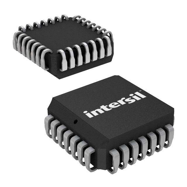
ICGOO电子元器件商城为您提供CS82C54Z96由Intersil设计生产,在icgoo商城现货销售,并且可以通过原厂、代理商等渠道进行代购。 CS82C54Z96价格参考。IntersilCS82C54Z96封装/规格:时钟/计时 - 可编程计时器和振荡器, Programmable Timer IC 8MHz 28-PLCC (11.51x11.51)。您可以下载CS82C54Z96参考资料、Datasheet数据手册功能说明书,资料中有CS82C54Z96 详细功能的应用电路图电压和使用方法及教程。
CS82C54Z96 是瑞萨电子(Renesas Electronics America Inc.)生产的一款可编程计时器/定时器电路,属于时钟和计时器件类别。它主要用于需要精确时间控制和脉冲信号生成的场景。

该芯片常用于以下应用场景:

1. 工业控制系统:如PLC(可编程逻辑控制器)、自动化设备中,用于实现精准的时间延迟、计数或周期性操作。
2. 通信设备:在数据通信系统中,用于波特率生成、帧同步控制等。
3. 测试与测量仪器:用于信号发生器、频率计、定时分析仪等设备中,提供高精度计时基准。
4. 嵌入式系统:作为微处理器或微控制器系统的辅助定时模块,管理中断、DMA传输、实时任务调度等。
5. 消费电子产品:如打印机、扫描仪等外设中,用于控制机械动作时序或接口同步。

该芯片具备多个独立的16位定时器通道,支持多种工作模式(如方波发生器、单稳态触发器、速率发生器等),具有良好的灵活性和可靠性,适合对时间和频率控制要求较高的应用场合。
| 参数 | 数值 |
| 产品目录 | 集成电路 (IC)半导体 |
| 描述 | IC OSC PROG TIMER 8MHZ 28PLCC计时器和支持产品 PERIPH PRG-CNTR 5V 8MHZ 28PLCC COM |
| 产品分类 | |
| 品牌 | Intersil |
| 产品手册 | |
| 产品图片 |
|
| rohs | 符合RoHS无铅 / 符合限制有害物质指令(RoHS)规范要求 |
| 产品系列 | 时钟和计时器IC,计时器和支持产品,Intersil CS82C54Z96- |
| 数据手册 | |
| 产品型号 | CS82C54Z96 |
| 产品目录页面 | |
| 产品种类 | 计时器和支持产品 |
| 传播延迟—最大值 | 150 ns at 5 V |
| 供应商器件封装 | 28-PLCC(11.51x11.51) |
| 其它名称 | CS82C54Z96DKR |
| 内部定时器数量 | 6 |
| 包装 | Digi-Reel® |
| 商标 | Intersil |
| 安装类型 | 表面贴装 |
| 安装风格 | SMD/SMT |
| 封装 | Reel |
| 封装/外壳 | 28-LCC(J 形引线) |
| 封装/箱体 | PLCC-28 |
| 工作温度 | 0°C ~ 70°C |
| 工厂包装数量 | 750 |
| 最大工作温度 | + 70 C |
| 最小工作温度 | 0 C |
| 标准包装 | 1 |
| 电压-电源 | 4.5 V ~ 5.5 V |
| 电流-电源 | 10mA |
| 电源电压-最大 | 5.5 V |
| 电源电压-最小 | 4.5 V |
| 电源电流 | 10 mA |
| 类型 | Programmable |
| 系列 | 82C54 |
| 计数 | - |
| 频率 | 8MHz |


- 商务部:美国ITC正式对集成电路等产品启动337调查
- 曝三星4nm工艺存在良率问题 高通将骁龙8 Gen1或转产台积电
- 太阳诱电将投资9.5亿元在常州建新厂生产MLCC 预计2023年完工
- 英特尔发布欧洲新工厂建设计划 深化IDM 2.0 战略
- 台积电先进制程称霸业界 有大客户加持明年业绩稳了
- 达到5530亿美元!SIA预计今年全球半导体销售额将创下新高
- 英特尔拟将自动驾驶子公司Mobileye上市 估值或超500亿美元
- 三星加码芯片和SET,合并消费电子和移动部门,撤换高东真等 CEO
- 三星电子宣布重大人事变动 还合并消费电子和移动部门
- 海关总署:前11个月进口集成电路产品价值2.52万亿元 增长14.8%


PDF Datasheet 数据手册内容提取
DATASHEET 82C54 FN2970 CMOS Programmable Interval Timer Rev 6.00 Sep 15, 2015 The Intersil 82C54 is a high performance CMOS Features Programmable Interval Timer manufactured using an • 8MHz to 12MHz Clock Input Frequency advanced 2micron CMOS process. • Compatible with NMOS 8254 The 82C54 has three independently programmable and - Enhanced Version of NMOS 8253 functional 16-bit counters, each capable of handling clock input frequencies of up to 8MHz (82C54) or 10MHz • Three Independent 16-Bit Counters (82C54-10) or 12MHz (82C54-12). • Six Programmable Counter Modes The high speed and industry standard configuration of the • Status Read Back Command 82C54 make it compatible with the Intersil 80C86, 80C88, and 80C286 CMOS microprocessors along with many • Binary or BCD Counting other industry standard processors. Six programmable • Fully TTL Compatible timer modes allow the 82C54 to be used as an event • Single 5V Power Supply counter, elapsed time indicator, programmable one-shot, and many other applications. Static CMOS circuit design • Low Power insures low power operation. - ICCSB. . . . . . . . . . . . . . . . . . . . . . . . . . . . . . . . . . .10µA The Intersil advanced CMOS process results in a significant - ICCOP . . . . . . . . . . . . . . . . . . . . . . . . . .10mA at 8MHz reduction in power with performance equal to or greater than • Operating Temperature Ranges existing equivalent products. - CX82C54 . . . . . . . . . . . . . . . . . . . . . . . . . 0°C to +70°C - IX82C54 . . . . . . . . . . . . . . . . . . . . . . . . .-40°C to +85°C - MD82C54. . . . . . . . . . . . . . . . . . . . . . .-55°C to +125°C • Pb-Free Plus Anneal Available (RoHS Compliant) Pinouts 82C54 (PDIP, CERDIP) 82C54 (PLCC/CLCC) TOP VIEW TOP VIEW D7 1 24 VCC D5 D6 D7 NC VCC WR RD 4 3 2 1 28 27 26 D6 2 23 WR D5 3 22 RD D4 5 25 NC D4 4 21 CS D3 6 24 CS D3 5 20 A1 D2 7 23 A1 D2 6 19 A0 D1 8 22 A0 D1 7 18 CLK 2 D0 9 21 CLK2 D0 8 17 OUT 2 CLK 0 10 20 OUT 2 CLK 0 9 16 GATE 2 NC 11 19 GATE 2 OUT 0 10 15 CLK 1 GATE 0 11 14 GATE 1 12 13 14 15 16 17 18 GND 12 13 OUT 1 UT 0 TE 0 GND NC UT 1 TE 1 LK 1 O A O A C G G FN2970 Rev 6.00 Page 1 of 23 Sep 15, 2015
82C54 Ordering Information PART NUMBERS TEMP RANGE PKG. 8MHz 10MHz 12MHz (°C) PACKAGE DWG. # CP82C54 CP82C54-10 (No longer available, CP82C54-12 0 to +70 24 Lead PDIP E24.6 recommended replacement: (No longer CP82C54-10Z) available, recommended replacement: CP82C54-12Z) CP82C54Z (See Note) CP82C54-10Z (See Note) CP82C54-12Z 0 to +70 24 Lead PDIP** (Pb-free) E24.6 (See Note) CS82C54* CS82C54-10* CS82C54-12 0 to +70 28 Lead PLCC N28.45 (No longer available, recommended replacement: CS82C54-12Z) CS82C54Z* (See Note) CS82C54-10Z* (See Note) CS82C54-12Z* 0 to +70 28 Lead PLCC (Pb-free) N28.45 (See Note) ID82C54 - - -40 to +85 24 Lead CERDIP F24.6 IP82C54 IP82C54-10 - -40 to +85 24 Lead PDIP E24.6 IP82C54Z (See Note) IP82C54-10Z (See Note) - -40 to +85 24 Lead PDIP** (Pb-free) E24.6 IS82C54* IS82C54-10* - -40 to +85 28 Lead PLCC N28.45 IS82C54Z (See Note) IS82C54-10Z (See Note) - -40 to +85 28 Lead PLCC (Pb-free) N28.45 MD82C54/B - - -55 to +125 24 Lead CERDIP F24.6 SMD # 8406501JA - - -55 to +125 24 Lead CERDIP F24.6 SMD# 84065013A - 84065023A -55 to +125 28 Lead CLCC J28.A Contact factory for availability. *Add “96” suffix for tape and reel. **Pb-free PDIPs can be used for through hole wave solder processing only. They are not intended for use in Reflow solder processing applications. NOTE: Intersil Pb-free plus anneal products employ special Pb-free material sets; molding compounds/die attach materials and 100% matte tin plate termination finish, which are RoHS compliant and compatible with both SnPb and Pb-free soldering operations. Intersil Pb-free products are MSL classified at Pb-free peak reflow temperatures that meet or exceed the Pb-free requirements of IPC/JEDEC J STD-020. FN2970 Rev 6.00 Page 2 of 23 Sep 15, 2015
82C54 Absolute Maximum Ratings Thermal Information Supply Voltage. . . . . . . . . . . . . . . . . . . . . . . . . . . . . . . . . . . . . +8.0V Thermal Resistance (Typical) JA (oC/W) JC (oC/W) Input, Output or I/O Voltage. . . . . . . . . . . . GND-0.5V to VCC +0.5V CERDIP Package. . . . . . . . . . . . . . . . . 55 12 ESD Classification. . . . . . . . . . . . . . . . . . . . . . . . . . . . . . . . .Class 1 CLCC Package . . . . . . . . . . . . . . . . . . 65 14 PDIP Package* . . . . . . . . . . . . . . . . . . 55 N/A Operating Conditions PLCC Package. . . . . . . . . . . . . . . . . . . 60 N/A Storage Temperature Range . . . . . . . . . . . . . . . . . .-65°C to +150°C Operating Voltage Range. . . . . . . . . . . . . . . . . . . . . .+4.5V to +5.5V Maximum Junction Temperature Ceramic Package . . . . . . .+175°C Operating Temperature Range Maximum Junction Temperature Plastic Package. . . . . . . . .+150°C CX82C54 . . . . . . . . . . . . . . . . . . . . . . . . . . . . . . . . . 0°C to +70°C Maximum Lead Temperature Package (Soldering 10s). . . . .+300°C IX82C54. . . . . . . . . . . . . . . . . . . . . . . . . . . . . . . . .-40°C to +85°C (PLCC - Lead Tips Only) MD82C54. . . . . . . . . . . . . . . . . . . . . . . . . . . . . . .-55°C to +125°C *Pb-free PDIPs can be used for through hole wave solder processing only. They are not intended for use in Reflow solder processing applications. Die Characteristics Gate Count . . . . . . . . . . . . . . . . . . . . . . . . . . . . . . . . . . .2250 Gates CAUTION: Stresses above those listed in “Absolute Maximum Ratings” may cause permanent damage to the device. This is a stress only rating and operation of the device at these or any other conditions above those indicated in the operational sections of this specification is not implied. DC Electrical Specifications VCC = +5.0V ± 10%, Includes all Temperature Ranges SYMBOL PARAMETER MIN MAX UNITS TEST CONDITIONS VIH Logical One Input Voltage 2.0 - V CX82C54, IX82C54 2.2 - V MD82C54 VIL Logical Zero Input Voltage - 0.8 V - VOH Output HIGH Voltage 3.0 - V IOH = -2.5mA VCC -0.4 - V IOH = -100A VOL Output LOW Voltage - 0.4 V IOL = +2.5mA II Input Leakage Current -1 +1 A VIN = GND or VCC DIP Pins 9,11,14-16,18-23 IO Output Leakage Current -10 +10 A VOUT = GND or VCC DIP Pins 1-8 ICCSB Standby Power Supply Current - 10 A VCC = 5.5V, VIN = GND or VCC, Outputs Open, Counters Programmed ICCOP Operating Power Supply Current - 10 mA VCC = 5.5V, CLK0 = CLK1 = CLK2 = 8MHz, VIN = GND or VCC, Outputs Open Capacitance TA = +25oC; All Measurements Referenced to Device GND, Note 1 SYMBOL PARAMETER TYP UNITS TEST CONDITIONS CIN Input Capacitance 20 pF FREQ = 1MHz COUT Output Capacitance 20 pF FREQ = 1MHz CI/O I/O Capacitance 20 pF FREQ = 1MHz NOTE: 1. Not tested, but characterized at initial design and at major process/design changes. FN2970 Rev 6.00 Page 3 of 23 Sep 15, 2015
82C54 AC Electrical SpecificationsVCC = +5.0V ± 10%, Includes all Temperature Ranges 82C54 82C54-10 82C54-12 TEST SYMBOL PARAMETER MIN MAX MIN MAX MIN MAX UNITS CONDITIONS READ CYCLE (1) TAR Address Stable Before RD 30 - 25 - 25 - ns 1 (2) TSR CS Stable Before RD 0 - 0 - 0 - ns 1 (3) TRA Address Hold Time After RD 0 - 0 - 0 - ns 1 (4) TRR RD Pulse Width 150 - 95 - 95 - ns 1 (5) TRD Data Delay from RD - 120 - 85 - 85 ns 1 (6) TAD Data Delay from Address - 210 - 185 - 185 ns 1 (7) TDF RD to Data Floating 5 85 5 65 5 65 ns 2, Note 1 (8) TRV Command Recovery Time 200 - 165 - 165 - ns WRITE CYCLE (9) TAW Address Stable Before WR 0 - 0 - 0 - ns (10) TSW CS Stable Before WR 0 - 0 - 0 - ns (11) TWA Address Hold Time After WR 0 - 0 - 0 - ns (12) TWW WR Pulse Width 95 - 95 - 95 - ns (13) TDW Data Setup Time Before WR 140 - 95 - 95 - ns (14) TWD Data Hold Time After WR 25 - 0 - 0 - ns (15) TRV Command Recovery Time 200 - 165 - 165 - ns CLOCK AND GATE (16) TCLK Clock Period 125 DC 100 DC 80 DC ns 1 (17) TPWH High Pulse Width 60 - 30 - 30 - ns 1 (18) TPWL Low Pulse Width 60 - 40 - 30 - ns 1 (19) TR Clock Rise Time - 25 - 25 - 25 ns (20) TF Clock Fall Time - 25 - 25 - 25 ns (21) TGW Gate Width High 50 - 50 - 50 - ns 1 (22) TGL Gate Width Low 50 - 50 - 50 - ns 1 (23) TGS Gate Setup Time to CLK 50 - 40 - 40 - ns 1 (24) TGH Gate Hold Time After CLK 50 - 50 - 50 - ns 1 (25) TOD Output Delay from CLK - 150 - 100 - 100 ns 1 (26) TODG Output Delay from Gate - 120 - 100 - 100 ns 1 (27) TWO OUT Delay from Mode Write - 260 - 240 - 240 ns 1 (28) TWC CLK Delay for Loading 0 55 0 55 0 55 ns 1 (29) TWG Gate Delay for Sampling -5 40 -5 40 -5 40 ns 1 (30) TCL CLK Setup for Count Latch -40 40 -40 40 -40 40 ns 1 NOTE: 1. Not tested, but characterized at initial design and at major process/design changes. FN2970 Rev 6.00 Page 4 of 23 Sep 15, 2015
82C54 Functional Diagram CLK 0 DATA/ COUNTER D7 - D0 8 BUS 0 GATE 0 INTERNAL BUS BUFFER OUT 0 CONTROL STATUS WORD LATCH REGISTER CRM CRL RD CLK 1 STATUS WR WRERAITDE/ BUS COU1NTER GATE 1 REGISTER A0 LOGIC L A OUT 1 A1 ERN CONTROL CE NT LOGIC CS I CLK 2 CONTROL COUNTER OLM OLL WORD GATE 2 2 REGISTER OUT 2 GATE n CLK n OUT n COUNTER INTERNAL BLOCK DIAGRAM Pin Description DIP PIN SYMBOL NUMBER TYPE DEFINITION D7 - D0 1 - 8 I/O DATA: Bi-directional three-state data bus lines, connected to system data bus. CLK 0 9 I CLOCK 0: Clock input of Counter 0. OUT 0 10 O OUT 0: Output of Counter 0. GATE 0 11 I GATE 0: Gate input of Counter 0. GND 12 GROUND: Power supply connection. OUT 1 13 O OUT 1: Output of Counter 1. GATE 1 14 I GATE 1: Gate input of Counter 1. CLK 1 15 I CLOCK 1: Clock input of Counter 1. GATE 2 16 I GATE 2: Gate input of Counter 2. OUT 2 17 O OUT 2: Output of Counter 2. CLK 2 18 I CLOCK 2: Clock input of Counter 2. A0, A1 19 - 20 I ADDRESS: Select inputs for one of the three counters or Control Word Register for read/write operations. Normally connected to the system address bus. A1 A0 SELECTS 0 0 Counter 0 0 1 Counter 1 1 0 Counter 2 1 1 Control Word Register CS 21 I CHIP SELECT: A low on this input enables the 82C54 to respond to RD and WR signals. RD and WR are ignored otherwise. RD 22 I READ: This input is low during CPU read operations. WR 23 I WRITE: This input is low during CPU write operations. VCC 24 - VCC: The +5V power supply pin. A 0.1F capacitor between pins VCC and GND is recommended for decoupling. FN2970 Rev 6.00 Page 5 of 23 Sep 15, 2015
82C54 Functional Description Read/Write Logic The Read/Write Logic accepts inputs from the system bus and General generates control signals for the other functional blocks of the The 82C54 is a programmable interval timer/counter designed 82C54. A1 and A0 select one of the three counters or the Control for use with microcomputer systems. It is a general purpose, Word Register to be read from/written into. A “low” on the RD multi-timing element that can be treated as an array of I/O input tells the 82C54 that the CPU is reading one of the counters. ports in the system software. A “low” on the WR input tells the 82C54 that the CPU is writing The 82C54 solves one of the most common problems in any either a Control Word or an initial count. Both RD and WR are microcomputer system, the generation of accurate time delays qualified by CS; RD and WR are ignored unless the 82C54 has under software control. Instead of setting up timing loops in been selected by holding CS low. software, the programmer configures the 82C54 to match his Control Word Register requirements and programs one of the counters for the desired The Control Word Register (Figure 2) is selected by the delay. After the desired delay, the 82C54 will interrupt the CPU. Read/Write Logic when A1, A0 = 11. If the CPU then does a Software overhead is minimal and variable length delays can write operation to the 82C54, the data is stored in the Control easily be accommodated. Word Register and is interpreted as a Control Word used to Some of the other computer/timer functions common to define the Counter operation. microcomputers which can be implemented with the 82C54 are: The Control Word Register can only be written to; status • Real time clock information is available with the Read-Back Command. • Event counter • Digital one-shot CLK 0 • Programmable rate generator DATA/ • Square wave generator D7 - D0 8 BUBFUFSER COU0NTER GATE 0 OUT 0 • Binary rate multiplier • Complex waveform generator • Complex motor controller Data Bus Buffer RD CLK 1 This three-state, bi-directional, 8-bit buffer is used to interface WR WRERAITDE/ BUS COU1NTER GATE 1 A0 LOGIC L the 82C54 to the system bus (see Figure 1). A OUT 1 A1 RN E T N CS I CLK 0 DATA/ D7 - D0 8 BUS COU0NTER GATE 0 CLK 2 BUFFER CONTROL COUNTER OUT 0 WORD 2 GATE 2 REGISTER OUT 2 RD CLK 1 WAR0 WLROERGAITDICE/ L BUS COU1NTER GATE 1 FIGURE 2. CONTROL WORD REGISTER AND COUNTER A OUT 1 FUNCTIONS A1 RN E NT Counter 0, Counter 1, Counter 2 CS I These three functional blocks are identical in operation, so only CLK 2 a single Counter will be described. The internal block diagram CONTROL COUNTER of a signal counter is shown in Figure 3. The counters are fully WORD GATE 2 2 REGISTER independent. Each Counter may operate in a different Mode. OUT 2 The Control Word Register is shown in the figure; it is not part of the Counter itself, but its contents determine how the Counter operates. FIGURE 1. DATA BUS BUFFER AND READ/WRITE LOGIC The status register, shown in the figure, when latched, contains FUNCTIONS the current contents of the Control Word Register and status of FN2970 Rev 6.00 Page 6 of 23 Sep 15, 2015
82C54 the output and null count flag. (See detailed explanation of the 82C54 System Interface Read-Back command.) The 82C54 is treated by the system software as an array of The actual counter is labeled CE (for Counting Element). It is a peripheral I/O ports; three are counters and the fourth is a 16-bit presettable synchronous down counter. control register for MODE programming. Basically, the select inputs A0, A1 connect to the A0, A1 INTERNAL BUS address bus signals of the CPU. The CS can be derived directly from the address bus using a linear select method or it can be connected to the output of a decoder. CONTROL STATUS WORD LATCH REGISTER Operational Description CRM CRL STATUS REGISTER General After power-up, the state of the 82C54 is undefined. The Mode, count value, and output of all Counters are undefined. CE CONTROL LOGIC How each Counter operates is determined when it is programmed. Each Counter must be programmed before it can be used. Unused counters need not be programmed. OLM OLL Programming the 82C54 Counters are programmed by writing a Control Word and then GATE n an initial count. CLK n OUT n All Control Words are written into the Control Word Register, which is selected when A1, A0 = 11. The Control Word FIGURE 3. COUNTER INTERNAL BLOCK DIAGRAM specifies which Counter is being programmed. OLM and OLL are two 8-bit latches. OL stands for “Output Latch”; By contrast, initial counts are written into the Counters, not the the subscripts M and L for “Most significant byte” and “Least Control Word Register. The A1, A0 inputs are used to select significant byte”, respectively. Both are normally referred to as one the Counter to be written into. The format of the initial count is unit and called just OL. These latches normally “follow” the CE, determined by the Control Word used. but if a suitable Counter Latch Command is sent to the 82C54, the latches “latch” the present count until read by the CPU and then ADDRESS BUS (16) return to “following” the CE. One latch at a time is enabled by the A1 A0 counter’s Control Logic to drive the internal bus. This is how the CONTROL BUS 16-bit Counter communicates over the 8-bit internal bus. Note that I/OR I/OW the CE itself cannot be read; whenever you read the count, it is DATA BUS (8) the OL that is being read. 8 Similarly, there are two 8-bit registers called CRM and CRL (for “Count Register”). Both are normally referred to as one unit and A1 A0 CS D0 - D7 RD WR 82C54 called just CR. When a new count is written to the Counter, the count is stored in the CR and later transferred to the CE. The COUNTER COUNTER COUNTER 0 1 2 Control Logic allows one register at a time to be loaded from the OUTGATECLK OUTGATECLK OUTGATECLK internal bus. Both bytes are transferred to the CE simultaneously. CRM and CRL are cleared when the Counter is programmed for one byte counts (either most significant byte only or least FIGURE 4. COUNTER INTERNAL BLOCK DIAGRAM significant byte only) the other byte will be zero. Note that the CE cannot be written into; whenever a count is written, it is written into Write Operations the CR. The programming procedure for the 82C54 is very flexible. The Control Logic is also shown in the diagram. CLK n, GATE Only two conventions need to be remembered: n, and OUT n are all connected to the outside world through 1. For Each Counter, the Control Word must be written before the Control Logic. the initial count is written. 2. The initial count must follow the count format specified in the Control Word (least significant byte only, most significant byte only, or least significant byte and then most significant byte). FN2970 Rev 6.00 Page 7 of 23 Sep 15, 2015
82C54 Since the Control Word Register and the three Counters have POSSIBLE PROGRAMMING SEQUENCE separate addresses (selected by the A1, A0 inputs), and each A1 A0 Control Word specifies the Counter it applies to (SC0, SC1 bits), no special instruction sequence is required. Any programming Control Word - Counter 0 1 1 sequence that follows the conventions above is acceptable. LSB of Count - Counter 0 0 0 CONTROL WORD FORMAT MSB of Count - Counter 0 0 0 A1, A0 = 11; CS = 0; RD = 1; WR = 0 Control Word - Counter 1 1 1 D7 D6 D5 D4 D3 D2 D1 D0 LSB of Count - Counter 1 0 1 SC1 SC0 RW1 RW0 M2 M1 M0 BCD MSB of Count - Counter 1 0 1 Control Word - Counter 2 1 1 SC - SELECT COUNTER LSB of Count - Counter 2 1 0 SC1 SC0 MSB of Count - Counter 2 1 0 0 0 Select Counter 0 0 1 Select Counter 1 POSSIBLE PROGRAMMING SEQUENCE 1 0 Select Counter 2 A1 A0 1 1 Read-Back Command (See Read Operations) Control Word - Counter 0 1 1 Control Word - Counter 1 1 1 RW - READ/WRITE Control Word - Counter 2 1 1 RW1 RW0 LSB of Count - Counter 2 1 0 0 0 Counter Latch Command (See Read Operations) LSB of Count - Counter 1 0 1 0 1 Read/Write least significant byte only. LSB of Count - Counter 0 0 0 1 0 Read/Write most significant byte only. MSB of Count - Counter 0 0 0 1 1 Read/Write least significant byte first, then most significant byte. MSB of Count - Counter 1 0 1 MSB of Count - Counter 2 1 0 M - MODE M2 M1 M0 POSSIBLE PROGRAMMING SEQUENCE 0 0 0 Mode 0 A1 A0 0 0 1 Mode 1 Control Word - Counter 2 1 1 X 1 0 Mode 2 Control Word - Counter 1 1 1 X 1 1 Mode 3 Control Word - Counter 0 1 1 1 0 0 Mode 4 LSB of Count - Counter 2 1 0 1 0 1 Mode 5 MSB of Count - Counter 2 1 0 LSB of Count - Counter 1 0 1 BCD - BINARY CODED DECIMAL MSB of Count - Counter 1 0 1 0 Binary Counter 16-bit LSB of Count - Counter 0 0 0 1 Binary Coded Decimal (BCD) Counter (4 Decades) MSB of Count - Counter 0 0 0 NOTE: Don’t Care bits (X) should be 0 to insure compatibility with future products. FN2970 Rev 6.00 Page 8 of 23 Sep 15, 2015
82C54 POSSIBLE PROGRAMMING SEQUENCE SC1, SC0 - specify counter to be latched A1 A0 SC1 SC0 COUNTER Control Word - Counter 1 1 1 0 0 0 Control Word - Counter 0 1 1 0 1 1 LSB of Count - Counter 1 0 1 1 0 2 Control Word - Counter 2 1 1 1 1 Read-Back Command LSB of Count - Counter 0 0 0 D5, D4 - 00 designates Counter Latch Command, X - Don’t Care. NOTE: Don’t Care bits (X) should be 0 to insure compatibility MSB of Count - Counter 1 0 1 with future products. LSB of Count - Counter 2 1 0 The selected Counter’s output latch (OL) latches the count when MSB of Count - Counter 0 0 0 the Counter Latch Command is received. This count is held in MSB of Count - Counter 2 1 0 the latch until it is read by the CPU (or until the Counter is NOTE: In all four examples, all counters are programmed to reprogrammed). The count is then unlatched automatically and Read/Write two-byte counts. These are only four of many the OL returns to “following” the counting element (CE). This programming sequences. allows reading the contents of the Counters “on the fly” without affecting counting in progress. Multiple Counter Latch A new initial count may be written to a Counter at any time Commands may be used to latch more than one Counter. Each without affecting the Counter’s programmed Mode in any way. latched Counter’s OL holds its count until read. Counter Latch Counting will be affected as described in the Mode definitions. Commands do not affect the programmed Mode of the Counter The new count must follow the programmed count format. in any way. If a Counter is programmed to read/write two-byte counts, the If a Counter is latched and then, some time later, latched again following precaution applies. A program must not transfer before the count is read, the second Counter Latch Command control between writing the first and second byte to another is ignored. The count read will be the count at the time the first routine which also writes into that same Counter. Otherwise, Counter Latch Command was issued. the Counter will be loaded with an incorrect count. With either method, the count must be read according to the READ OPERATIONS programmed format; specifically, if the Counter is programmed It is often desirable to read the value of a Counter without for two byte counts, two bytes must be read. The two bytes do disturbing the count in progress. This is easily done in the not have to be read one right after the other; read or write or 82C54. programming operations of other Counters may be inserted between them. There are three possible methods for reading the Counters. The first is through the Read-Back command, which is Another feature of the 82C54 is that reads and writes of the explained later. The second is a simple read operation of the same Counter may be interleaved; for example, if the Counter Counter, which is selected with the A1, A0 inputs. The only is programmed for two byte counts, the following sequence is requirement is that the CLK input of the selected Counter must valid. be inhibited by using either the GATE input or external logic. 1. Read least significant byte. Otherwise, the count may be in process of changing when it is read, giving an undefined result. 2. Write new least significant byte. 3. Read most significant byte. COUNTER LATCH COMMAND 4. Write new most significant byte. The other method for reading the Counters involves a special If a counter is programmed to read or write two-byte counts, software command called the “Counter Latch Command”. Like the following precaution applies: A program MUST NOT a Control Word, this command is written to the Control Word transfer control between reading the first and second byte to Register, which is selected when A1, A0 = 11. Also, like a another routine which also reads from that same Counter. Control Word, the SC0, SC1 bits select one of the three Otherwise, an incorrect count will be read. Counters, but two other bits, D5 and D4, distinguish this command from a Control Word. READ-BACK COMMAND . The read-back command allows the user to check the count A1, A0 = 11; CS = 0; RD = 1; WR = 0 value, programmed Mode, and current state of the OUT pin and Null Count flag of the selected counter(s). D7 D6 D5 D4 D3 D2 D1 D0 The command is written into the Control Word Register and SC1 SC0 0 0 X X X X has the format shown in Figure 5. The command applies to the FN2970 Rev 6.00 Page 9 of 23 Sep 15, 2015
82C54 counters selected by setting their corresponding bits D3, D2, NULL COUNT bit D6 indicates when the last count written to the D1 = 1. counter register (CR) has been loaded into the counting element (CE). The exact time this happens depends on the Mode of the A0, A1 = 11; CS = 0; RD = 1; WR = 0 counter and is described in the Mode Definitions, but until the D7 D6 D5 D4 D3 D2 D1 D0 counter is loaded into the counting element (CE), it can’t be read from the counter. If the count is latched or read before this time, 1 1 COUNT STATUS CNT 2 CNT 1 CNT 0 0 the count value will not reflect the new count just written. The D5:0=Latch count of selected Counter (s) operation of Null Count is shown below. D4:0=Latch status of selected Counter(s) D3:1=Select Counter 2 THIS ACTION: CAUSES: D2:1=Select Counter 1 A. Write to the control word register:(1) . . . . Null Count = 1 D1:1=Select Counter 0 D0:Reserved for future expansion; Must be 0 B. Write to the count register (CR):(2) . . . . . Null Count = 1 FIGURE 5. READ-BACK COMMAND FORMAT C. New count is loaded into CE (CR - CE). . Null Count = 0 The read-back command may be used to latch multiple 1. Only the counter specified by the control word will have its null count set to 1. Null count bits of other counters are counter output latches (OL) by setting the COUNT bit D5 = 0 unaffected. and selecting the desired counter(s). This signal command is functionally equivalent to several counter latch commands, one 2. If the counter is programmed for two-byte counts (least significant byte then most significant byte) null count goes for each counter latched. Each counter’s latched count is held to 1 when the second byte is written. until it is read (or the counter is reprogrammed). That counter is automatically unlatched when read, but other counters remain If multiple status latch operations of the counter(s) are latched until they are read. If multiple count read-back performed without reading the status, all but the first are ignored; commands are issued to the same counter without reading the i.e., the status that will be read is the status of the counter at the count, all but the first are ignored; i.e., the count which will be time the first status read-back command was issued. read is the count at the time the first read-back command was Both count and status of the selected counter(s) may be issued. latched simultaneously by setting both COUNT and STATUS The read-back command may also be used to latch status bits D5, D4 = 0. This is functionally the same as issuing two information of selected counter(s) by setting STATUS bit D4 = separate read-back commands at once, and the above 0. Status must be latched to be read; status of a counter is discussions apply here also. Specifically, if multiple count accessed by a read from that counter. and/or status read-back commands are issued to the same counter(s) without any intervening reads, all but the first are The counter status format is shown in Figure 6. Bits D5 through ignored. This is illustrated in Figure 7. D0 contain the counter’s programmed Mode exactly as written in the last Mode Control Word. OUTPUT bit D7 contains the If both count and status of a counter are latched, the first read current state of the OUT pin. This allows the user to monitor operation of that counter will return latched status, regardless the counter’s output via software, possibly eliminating some of which was latched first. The next one or two reads hardware from a system. (depending on whether the counter is programmed for one or two type counts) return latched count. Subsequent reads D7 D6 D5 D4 D3 D2 D1 D0 return unlatched count. OUTPUT NULL RW1 RW0 M2 M1 M0 BCD COUNT D7:1=Out pin is 1 0=Out pin is 0 D6:1=Null count 0=Count available for reading D5-D0=Counter programmed mode (See Control Word Formats) FIGURE 6. STATUS BYTE FN2970 Rev 6.00 Page 10 of 23 Sep 15, 2015
82C54 COMMANDS D7 D6 D5 D4 D3 D2 D1 D0 DESCRIPTION RESULT 1 1 0 0 0 0 1 0 Read-Back Count and Status of Counter 0 Count and Status Latched for Counter 0 1 1 1 0 0 1 0 0 Read-Back Status of Counter 1 Status Latched for Counter 1 1 1 1 0 1 1 0 0 Read-Back Status of Counters 2, 1 Status Latched for Counter 2, But Not Counter 1 1 1 0 1 1 0 0 0 Read-Back Count of Counter 2 Count Latched for Counter 2 1 1 0 0 0 1 0 0 Read-Back Count and Status of Counter 1 Count Latched for Counter 1, But Not Status 1 1 1 0 0 0 1 0 Read-Back Status of Counter 1 Command Ignored, Status Already Latched for Counter 1 FIGURE 7. READ-BACK COMMAND EXAMPLE MODE 0: INTERRUPT ON TERMINAL COUNT CS RD WR A1 A0 Mode 0 is typically used for event counting. After the Control 0 1 0 0 0 Write into Counter 0 Word is written, OUT is initially low, and will remain low until 0 1 0 0 1 Write into Counter 1 the Counter reaches zero. OUT then goes high and remains high until a new count or a new Mode 0 Control Word is written 0 1 0 1 0 Write into Counter 2 to the Counter. 0 1 0 1 1 Write Control Word GATE = 1 enables counting; GATE = 0 disables counting. 0 0 1 0 0 Read from Counter 0 GATE has no effect on OUT. 0 0 1 0 1 Read from Counter 1 After the Control Word and initial count are written to a 0 0 1 1 0 Read from Counter 2 Counter, the initial count will be loaded on the next CLK pulse. 0 0 1 1 1 No-Operation (Three-State) This CLK pulse does not decrement the count, so for an initial count of N, OUT does not go high until N + 1 CLK pulses after 1 X X X X No-Operation (Three-State) the initial count is written. 0 1 1 X X No-Operation (Three-State) If a new count is written to the Counter it will be loaded on the FIGURE 8. READ/WRITE OPERATIONS SUMMARY next CLK pulse and counting will continue from the new count. If a two-byte count is written, the following happens: MODE DEFINITIONS The following are defined for use in describing the operation of 1. Writing the first byte disables counting. Out is set low the 82C54. immediately (no clock pulse required). 2. Writing the second byte allows the new count to be loaded CLK PULSE - A rising edge, then a falling edge, in that order, on the next CLK pulse. of a Counter’s CLK input. This allows the counting sequence to be synchronized by TRIGGER - A rising edge of a Counter’s Gate input. software. Again OUT does not go high until N + 1 CLK pulses after the new count of N is written. COUNTER LOADING - The transfer of a count from the CR to the CE (See “Functional Description”) FN2970 Rev 6.00 Page 11 of 23 Sep 15, 2015
82C54 If an initial count is written while GATE = 0, it will still be loaded MODE 1: HARDWARE RETRIGGERABLE ONE-SHOT on the next CLK pulse. When GATE goes high, OUT will go OUT will be initially high. OUT will go low on the CLK pulse high N CLK pulses later; no CLK pulse is needed to load the following a trigger to begin the one-shot pulse, and will remain counter as this has already been done. low until the Counter reaches zero. OUT will then go high and remain high until the CLK pulse after the next trigger. CW = 10 LSB = 4 WR After writing the Control Word and initial count, the Counter is armed. A trigger results in loading the Counter and setting OUT CLK low on the next CLK pulse, thus starting the one-shot pulse N CLK cycles in duration. The one-shot is retriggerable, hence GATE OUT will remain low for N CLK pulses after any trigger. The one- OUT shot pulse can be repeated without rewriting the same count into N N N N 04 03 02 01 00 FFFF FFFE the counter. GATE has no effect on OUT. If a new count is written to the Counter during a one-shot CW = 10 LSB = 3 pulse, the current one-shot is not affected unless the Counter WR is retriggerable. In that case, the Counter is loaded with the new count and the one-shot pulse continues until the new CLK count expires. GATE CW = 12 LSB = 3 OUT WR 0 0 0 0 0 0 FF N N N N 3 2 2 2 1 0 FF CLK CW = 10 LSB = 3 LSB = 2 GATE WR CLK OUT 0 0 0 0 FF 0 0 GATE N N N N N 3 2 1 0 FF 3 2 OUT CW = 12 LSB = 3 0 0 0 0 0 0 FF N N N N 3 2 1 2 1 0 FF WR FIGURE 9. MODE 0 CLK NOTES: The following conventions apply to all mode timing diagrams. 1. Counters are programmed for binary (not BCD) counting and for reading/writing least significant byte (LSB) only. GATE 2. The counter is always selected (CS always low). 3. CW stands for “Control Word”; CW = 10 means a control word of 10, OUT Hex is written to the counter. 0 0 0 0 0 0 0 4. LSB stands for Least significant “byte” of count. N N N N N 3 2 1 3 2 1 0 5. Numbers below diagrams are count values. The lower number is the least significant byte. The upper number is the most significant CW = 12 LSB = 2 LSB = 4 byte. Since the counter is programmed to read/write LSB only, the WR most significant byte cannot be read. 6. N stands for an undefined count. CLK 7. Vertical lines show transitions between count values. GATE OUT 0 0 0 FF FF 0 0 N N N N N 2 1 0 FF FE 4 3 FIGURE 10. MODE 1 FN2970 Rev 6.00 Page 12 of 23 Sep 15, 2015
82C54 MODE 2: RATE GENERATOR MODE 3: SQUARE WAVE MODE This Mode functions like a divide-by-N counter. It is typically Mode 3 is typically used for Baud rate generation. Mode 3 is used to generate a Real Time Clock Interrupt. OUT will initially similar to Mode 2 except for the duty cycle of OUT. OUT will be high. When the initial count has decremented to 1, OUT initially be high. When half the initial count has expired, OUT goes low for one CLK pulse. OUT then goes high again, the goes low for the remainder of the count. Mode 3 is periodic; the Counter reloads the initial count and the process is repeated. sequence above is repeated indefinitely. An initial count of N Mode 2 is periodic; the same sequence is repeated indefinitely. results in a square wave with a period of N CLK cycles. For an initial count of N, the sequence repeats every N CLK cycles. GATE = 1 enables counting; GATE = 0 disables counting. If GATE goes low while OUT is low, OUT is set high immediately; GATE = 1 enables counting; GATE = 0 disables counting. If no CLK pulse is required. A trigger reloads the Counter with GATE goes low during an output pulse, OUT is set high immediately. A trigger reloads the Counter with the initial count the initial count on the next CLK pulse. Thus the GATE input on the next CLK pulse; OUT goes low N CLK pulses after the can be used to synchronize the Counter. trigger. Thus the GATE input can be used to synchronize the After writing a Control Word and initial count, the Counter will Counter. be loaded on the next CLK pulse. This allows the Counter to be After writing a Control Word and initial count, the Counter will synchronized by software also. be loaded on the next CLK pulse. OUT goes low N CLK pulses after the initial count is written. This allows the Counter to be Writing a new count while counting does not affect the current synchronized by software also. counting sequence. If a trigger is received after writing a new count but before the end of the current half-cycle of the square Writing a new count while counting does not affect the current wave, the Counter will be loaded with the new count on the counting sequence. If a trigger is received after writing a new next CLK pulse and counting will continue from the new count. count but before the end of the current period, the Counter will be Otherwise, the new count will be loaded at the end of the loaded with the new count on the next CLK pulse and counting will continue from the end of the current counting cycle. current half-cycle. CW = 14 LSB = 3 CW = 16 LSB = 4 WR WR CLK CLK GATE GATE OUT OUT 0 0 0 0 0 0 0 N N N N 3 2 1 3 2 1 3 N N N N 0 0 0 0 0 0 0 0 0 0 4 2 4 2 4 2 4 2 4 2 CW = 14 LSB = 3 CW = 16 LSB = 5 WR WR CLK CLK GATE GATE OUT OUT 0 0 0 0 0 0 0 0 0 0 N N N N 0 0 0 0 0 0 0 5 4 2 5 2 5 4 2 5 2 N N N N 3 2 2 3 2 1 3 CW = 16 LSB = 4 CW = 14 LSB = 4 LSB = 5 WR WR CLK CLK GATE GATE OUT OUT 0 0 0 0 0 0 0 N N N N 4 3 2 1 5 4 3 0 0 0 0 0 0 0 0 0 0 N N N N 4 2 4 2 2 2 4 2 4 2 FIGURE 11. MODE 2 FIGURE 12. MODE 3 FN2970 Rev 6.00 Page 13 of 23 Sep 15, 2015
82C54 Mode 3 Is Implemented As Follows CW = 18 LSB = 3 EVEN COUNTS - OUT is initially high. The initial count is WR loaded on one CLK pulse and then is decremented by two on succeeding CLK pulses. When the count expires, OUT CLK changes value and the Counter is reloaded with the initial count. The above process is repeated indefinitely. GATE ODD COUNTS - OUT is initially high. The initial count is loaded OUT on one CLK pulse, decremented by one on the next CLK pulse, 0 0 0 0 FF FF FF and then decremented by two on succeeding CLK pulses. When N N N N 3 2 1 0 FF FE FD the count expires, OUT goes low and the Counter is reloaded with CW = 18 LSB = 3 the initial count. The count is decremented by three on the next CLK pulse, and then by two on succeeding CLK pulses. When the WR count expires, OUT goes high again and the Counter is reloaded with the initial count. The above process is repeated indefinitely. CLK So for odd counts, OUT will be high for (N + 1)/2 counts and low for (N - 1)/2 counts. GATE MODE 4: SOFTWARE TRIGGERED MODE OUT OUT will be initially high. When the initial count expires, OUT 0 0 0 0 0 0 FF will go low for one CLK pulse then go high again. The counting N N N N 3 3 3 2 1 0 FF sequence is “Triggered” by writing the initial count. CW = 18 LSB = 3 LSB = 2 GATE = 1 enables counting; GATE = 0 disables counting. WR GATE has no effect on OUT. CLK After writing a Control Word and initial count, the Counter will be loaded on the next CLK pulse. This CLK pulse does not GATE decrement the count, so for an initial count of N, OUT does not strobe low until N + 1 CLK pulses after the initial count is written. OUT 0 0 0 0 0 0 FF If a new count is written during counting, it will be loaded on the N N N N 3 2 1 2 1 0 FF next CLK pulse and counting will continue from the new count. FIGURE 13. MODE 4 If a two-byte count is written, the following happens: 1. Writing the first byte has no effect on counting. MODE 5: HARDWARE TRIGGERED STROBE (RETRIGGERABLE) 2. Writing the second byte allows the new count to be loaded on the next CLK pulse. OUT will initially be high. Counting is triggered by a rising edge This allows the sequence to be “retriggered” by software. OUT of GATE. When the initial count has expired, OUT will go low strobes low N + 1 CLK pulses after the new count of N is written. for one CLK pulse and then go high again. After writing the Control Word and initial count, the counter will not be loaded until the CLK pulse after a trigger. This CLK pulse does not decrement the count, so for an initial count of N, OUT does not strobe low until N + 1 CLK pulses after trigger. A trigger results in the Counter being loaded with the initial count on the next CLK pulse. The counting sequence is triggerable. OUT will not strobe low for N + 1 CLK pulses after any trigger GATE has no effect on OUT. If a new count is written during counting, the current counting sequence will not be affected. If a trigger occurs after the new count is written but before the current count expires, the FN2970 Rev 6.00 Page 14 of 23 Sep 15, 2015
82C54 Counter will be loaded with new count on the next CLK pulse Counter and counting will continue from there. New counts are loaded and Counters are decremented on the CW = 1A LSB = 3 falling edge of CLK. WR The largest possible initial count is 0; this is equivalent to 216 for binary counting and 104 for BCD counting. CLK The counter does not stop when it reaches zero. In Modes 0, 1, GATE 4, and 5 the Counter “wraps around” to the highest count, either FFFF hex for binary counting or 9999 for BCD counting, OUT and continues counting. Modes 2 and 3 are periodic; the Counter reloads itself with the initial count and continues 0 0 0 0 FF 0 N N N N N 3 2 1 0 FF 3 counting from there. CW = 1A LSB = 3 SIGNAL STATUS LOW OR WR MODES GOING LOW RISING HIGH 0 Disables Counting - Enables Counting CLK 1 - 1) Initiates - GATE Counting 2) Resets output after next clock OUT 2 1) Disables Initiates Counting Enables Counting 0 0 0 0 0 0 FF N N N N N N 3 2 3 2 1 0 FF counting 2) Sets output CW = 1A LSB = 3 LSB = 5 immediately high WR 3 1) Disables Initiates Counting Enables Counting counting 2) Sets output CLK immediately high GATE 4 1) Disables - Enables Counting Counting OUT 5 - Initiates Counting - 0 0 0 0 FF FF 0 0 FIGURE 15. GATE PIN OPERATIONS SUMMARY N N N N N 3 2 1 0 FF FE 5 4 FIGURE 14. MODE 5 MODE MIN COUNT MAX COUNT Operation Common To All Modes 0 1 0 1 1 0 Programming 2 2 0 When a Control Word is written to a Counter, all Control Logic, is immediately reset and OUT goes to a known initial state; no 3 2 0 CLK pulses are required for this. 4 1 0 Gate 5 1 0 The GATE input is always sampled on the rising edge of CLK. NOTE: 0 is equivalent to 216 for binary counting and 104 for BCD In Modes 0, 2, 3 and 4 the GATE input is level sensitive, and counting. logic level is sampled on the rising edge of CLK. In modes 1, 2, FIGURE 16. MINIMUM AND MAXIMUM INITIAL COUNTS 3 and 5 the GATE input is rising-edge sensitive. In these Modes, a rising edge of Gate (trigger) sets an edge-sensitive flip-flop in the Counter. This flip-flop is then sampled on the next rising edge of CLK. The flip-flop is reset immediately after it is sampled. In this way, a trigger will be detected no matter when it occurs - a high logic level does not have to be maintained until the next rising edge of CLK. Note that in Modes 2 and 3, the GATE input is both edge-and level- sensitive. FN2970 Rev 6.00 Page 15 of 23 Sep 15, 2015
82C54 Timing Waveforms A0 - A1 (9) tWA (11) tAW CS (10) tSW DATA BUS VALID (13) tDW tWD (14) WR (12) tWW FIGURE 17. WRITE A0 - A1 tAR (1) tRA (3) CS (2) tSR (4) tRR RD (5) (7) tRD tDF (6) DATA BUS tAD VALID FIGURE 18. READ (8) (15) tRV RD, WR FIGURE 19. RECOVERY FN2970 Rev 6.00 Page 16 of 23 Sep 15, 2015
82C54 Timing Waveforms (Continued) COUNT MODE (SEE NOTE) WR tWC (28) (16) (23) tGS (17) tCLK tCL (30) tPWH (18) CLK tPWL (19) tF (20) tR tGS tGH (24) (23) GATE (21) (24) tGW (22) tGH tGL tOD (25) OUT (27) tODG (26) tWO NOTE: LAST BYTE OF COUNT BEING WRITTEN FIGURE 20. CLOCK AND GATE Burn-In Circuits MD82C54 (CERDIP) MR82C54 (CLCC) VCC C1 VCC C1 R1 Q1 1 24 R1 R1 VCC Q2 Q1OPEN Q3 VCC Q2 2 23 Q3 R1 R1 R1 R1 R1 R1 R1 VCC 3 22 VCC R1 R1 GND 4 21 GND F9 R1 5 20 R1 Q5 VCC R1 4 3 2 1 28 27 26 R1 R1 GND 5 25 OPEN F10 6 19 Q4 F11 RR11 7 18 R2 F2 R3 F9 RR11 6 24 RR11 GND F12 8 17 A F10 7 23 Q5 F0 R2 9 16 R1 Q8 A F11 R1 8 22 R1 Q4 R2 R4 A 10 15 F1 R1 R2 R1 R1 F12 9 21 F2 Q6 11 14 Q7 R2 R5 F0 10 20 VCC/2 GND 12 13 A R1 OPEN 11 19 Q8 12 13 14 15 16 17 18 R5 R1 R5 R1 R2 VCC/2Q6 GND VCC/2Q7 F1 OPEN NOTES: 1. VCC = 5.5V 0.5V 2. GND = 0V 3. VIH = 4.5V 10% 4. VIL = -0.2V to 0.4V 5. R1 = 47k 5% 6. R2 = 1.0k 5% 7. R3 = 2.7k 5% 8. R4 = 1.8k 5% 9. R5 = 1.2k 5% 10. C1 = 0.01F Min 11. F0 = 100kHz10% 12. F1 = F0/2, F2 = F1/2, ...F12 = F11/2 FN2970 Rev 6.00 Page 17 of 23 Sep 15, 2015
82C54 Die Characteristics METALLIZATION: Type: Si-Al-Cu DIE DIMENSIONS: Thickness: Metal 1: 8kÅ ± 0.75kÅ 129mils x 155mils x 19mils Metal 2: 12kÅ ± 1.0kÅ (3270µm x 3940µm x 483µm) GLASSIVATION: Type: Nitrox Thickness: 10kÅ ± 3.0kÅ Metallization Mask Layout 82C54 D5 D6 D7 VCC WR RD D4 CS D3 A1 D2 A0 D1 CLK2 D0 OUT2 CLK0 GATE2 OUT0 GATE0 GND OUT1 GATE1 CLK1 FN2970 Rev 6.00 Page 18 of 23 Sep 15, 2015
82C54 Revision History The revision history provided is for informational purposes only and is believed to be accurate, but not warranted. Please go to the web to make sure that you have the latest revision. DATE REVISION CHANGE September 15, 2015 FN2970.6 - Updated Ordering Information Table on page2. - Added Revision History. About Intersil Intersil Corporation is a leading provider of innovative power management and precision analog solutions. The company's products address some of the largest markets within the industrial and infrastructure, mobile computing and high-end consumer markets. For the most updated datasheet, application notes, related documentation and related parts, please see the respective product information page found at www.intersil.com. You may report errors or suggestions for improving this datasheet by visiting www.intersil.com/ask. Reliability reports are also available from our website at www.intersil.com/support. FN2970 Rev 6.00 Page 19 of 23 Sep 15, 2015
82C54 Dual-In-Line Plastic Packages (PDIP) E24.6 (JEDEC MS-011-AA ISSUE B) N 24 LEAD DUAL-IN-LINE PLASTIC PACKAGE E1 IANRDEEAX 1 2 3 N/2 INCHES MILLIMETERS SYMBOL MIN MAX MIN MAX NOTES -B- A - 0.250 - 6.35 4 -A- D E A1 0.015 - 0.39 - 4 BASE A2 0.125 0.195 3.18 4.95 - PLANE A2 -C- A B 0.014 0.022 0.356 0.558 - SEATING PLANE L CL B1 0.030 0.070 0.77 1.77 8 D1 D1 A1 eA C 0.008 0.015 0.204 0.381 - B1 e eC C D 1.150 1.290 29.3 32.7 5 B eB D1 0.005 - 0.13 - 5 0.010 (0.25) M C A B S E 0.600 0.625 15.24 15.87 6 NOTES: E1 0.485 0.580 12.32 14.73 5 1. Controlling Dimensions: INCH. In case of conflict between English and e 0.100 BSC 2.54 BSC - Metric dimensions, the inch dimensions control. eA 0.600 BSC 15.24 BSC 6 2. Dimensioning and tolerancing per ANSI Y14.5M-1982. eB - 0.700 - 17.78 7 3. Symbols are defined in the “MO Series Symbol List” in Section 2.2 of Publication No. 95. L 0.115 0.200 2.93 5.08 4 4. Dimensions A, A1 and L are measured with the package seated in N 24 24 9 JEDEC seating plane gauge GS-3. Rev. 0 12/93 5. D, D1, and E1 dimensions do not include mold flash or protrusions. Mold flash or protrusions shall not exceed 0.010 inch (0.25mm). 6. E and eA are measured with the leads constrained to be perpendic- ular to datum -C- . 7. eB and eC are measured at the lead tips with the leads unconstrained. eC must be zero or greater. 8. B1 maximum dimensions do not include dambar protrusions. Dambar protrusions shall not exceed 0.010 inch (0.25mm). 9. N is the maximum number of terminal positions. 10. Corner leads (1, N, N/2 and N/2 + 1) for E8.3, E16.3, E18.3, E28.3, E42.6 will have a B1 dimension of 0.030 - 0.045 inch (0.76 - 1.14mm). FN2970 Rev 6.00 Page 20 of 23 Sep 15, 2015
82C54 Plastic Leaded Chip Carrier Packages (PLCC) 0.042 (1.07) N28.45 (JEDEC MS-018AB ISSUE A) 0.042 (1.07) 0.048 (1.22) 0.004 (0.10) C 28 LEAD PLASTIC LEADED CHIP CARRIER PACKAGE 0.056 (1.42) PIN (1) IDENTIFIER 0.050 (1.27) TP 0.025 (0.64) INCHES MILLIMETERS R 0.045 (1.14) CL SYMBOL MIN MAX MIN MAX NOTES A 0.165 0.180 4.20 4.57 - A1 0.090 0.120 2.29 3.04 - D2/E2 D 0.485 0.495 12.32 12.57 - CL D1 0.450 0.456 11.43 11.58 3 E1 E D2 0.191 0.219 4.86 5.56 4, 5 D2/E2 E 0.485 0.495 12.32 12.57 - VIEW “A” E1 0.450 0.456 11.43 11.58 3 E2 0.191 0.219 4.86 5.56 4, 5 0.020 (0.51) N 28 28 6 MIN D1 A1 Rev. 2 11/97 D A SEATING 0.020 (0.51) MAX -C- PLANE 3 PLCS 0.026 (0.66) 0.032 (0.81) 0.013 (0.33) 0.021 (0.53) 0.025 (0.64) 0.045 (1.14) MIN MIN VIEW “A” TYP. NOTES: 1. Controlling dimension: INCH. Converted millimeter dimensions are not necessarily exact. 2. Dimensions and tolerancing per ANSI Y14.5M-1982. 3. Dimensions D1 and E1 do not include mold protrusions. Allowable mold protrusion is 0.010 inch (0.25mm) per side. Dimensions D1 and E1 include mold mismatch and are measured at the extreme material condition at the body parting line. 4. To be measured at seating plane -C- contact point. 5. Centerline to be determined where center leads exit plastic body. 6. “N” is the number of terminal positions. FN2970 Rev 6.00 Page 21 of 23 Sep 15, 2015
82C54 Ceramic Leadless Chip Carrier Packages (CLCC) J28.A MIL-STD-1835 CQCC1-N28 (C-4) 0.010S E HS 28 PAD CERAMIC LEADLESS CHIP CARRIER PACKAGE D INCHES MILLIMETERS D3 SYMBOL MIN MAX MIN MAX NOTES j x 45o A 0.060 0.100 1.52 2.54 6, 7 A1 0.050 0.088 1.27 2.23 - B - - - - - B1 0.022 0.028 0.56 0.71 2, 4 B2 0.072 REF 1.83 REF - E3 E B B3 0.006 0.022 0.15 0.56 - D 0.442 0.460 11.23 11.68 - D1 0.300 BSC 7.62 BSC - D2 0.150 BSC 3.81 BSC - h x 45o D3 - 0.460 - 11.68 2 0.010 S E F S E 0.442 0.460 11.23 11.68 - A A1 E1 0.300 BSC 7.62 BSC - E2 0.150 BSC 3.81 BSC - PLANE 2 E3 - 0.460 - 11.68 2 e 0.050 BSC 1.27 BSC - PLANE 1 -E- e1 0.015 - 0.38 - 2 h 0.040 REF 1.02 REF 5 j 0.020 REF 0.51 REF 5 0.007M E F S HS L 0.045 0.055 1.14 1.40 - B1 L1 0.045 0.055 1.14 1.40 - e L3 L2 0.075 0.095 1.90 2.41 - L -H- L3 0.003 0.015 0.08 0.038 - ND 7 7 3 NE 7 7 3 N 28 28 3 -F- Rev. 0 5/18/94 B3 NOTES: E1 1. Metallized castellations shall be connected to plane 1 terminals and extend toward plane 2 across at least two layers of ceramic E2 L2 or completely across all of the ceramic layers to make electrical B2 connection with the optional plane 2 terminals. 2. Unless otherwise specified, a minimum clearance of 0.015 inch (0.38mm) shall be maintained between all metallized features L1 (e.g., lid, castellations, terminals, thermal pads, etc.) e1 D2 3. Symbol “N” is the maximum number of terminals. Symbols “ND” and “NE” are the number of terminals along the sides of length D1 “D” and “E”, respectively. 4. The required plane 1 terminals and optional plane 2 terminals (if used) shall be electrically connected. 5. The corner shape (square, notch, radius, etc.) may vary at the manufacturer’s option, from that shown on the drawing. 6. Chip carriers shall be constructed of a minimum of two ceramic layers. 7. Dimension “A” controls the overall package thickness. The maxi- mum “A” dimension is package height before being solder dipped. 8. Dimensioning and tolerancing per ANSI Y14.5M-1982. 9. Controlling dimension: INCH. FN2970 Rev 6.00 Page 22 of 23 Sep 15, 2015
82C54 Ceramic Dual-In-Line Frit Seal Packages (CERDIP) c1 LEAD FINISH F24.6 MIL-STD-1835 GDIP1-T24 (D-3, CONFIGURATION A) 24 LEAD CERAMIC DUAL-IN-LINE FRIT SEAL PACKAGE -A- -D- INCHES MILLIMETERS BASE (c) METAL SYMBOL MIN MAX MIN MAX NOTES E b1 A - 0.225 - 5.72 - M M -B- (b) b 0.014 0.026 0.36 0.66 2 b1 0.014 0.023 0.36 0.58 3 SECTION A-A bbb S C A - B S D S b2 0.045 0.065 1.14 1.65 - D BASE b3 0.023 0.045 0.58 1.14 4 PLANE Q -C- A c 0.008 0.018 0.20 0.46 2 SEATING PLANE L c1 0.008 0.015 0.20 0.38 3 D - 1.290 - 32.77 5 S1 A A eA b2 E 0.500 0.610 12.70 15.49 5 b e eA/2 c e 0.100 BSC 2.54 BSC - ccc M C A - B S D S aaaM C A - B S D S eA 0.600 BSC 15.24 BSC - eA/2 0.300 BSC 7.62 BSC - NOTES: 1. Index area: A notch or a pin one identification mark shall be locat- L 0.120 0.200 3.05 5.08 - ed adjacent to pin one and shall be located within the shaded Q 0.015 0.075 0.38 1.91 6 area shown. The manufacturer’s identification shall not be used S1 0.005 - 0.13 - 7 as a pin one identification mark. 2. The maximum limits of lead dimensions b and c or M shall be 90o 105o 90o 105o - measured at the centroid of the finished lead surfaces, when aaa - 0.015 - 0.38 - solder dip or tin plate lead finish is applied. bbb - 0.030 - 0.76 - 3. Dimensions b1 and c1 apply to lead base metal only. Dimension M applies to lead plating and finish thickness. ccc - 0.010 - 0.25 - 4. Corner leads (1, N, N/2, and N/2+1) may be configured with a M - 0.0015 - 0.038 2, 3 partial lead paddle. For this configuration dimension b3 replaces N 24 24 8 dimension b2. Rev. 0 4/94 5. This dimension allows for off-center lid, meniscus, and glass overrun. 6. Dimension Q shall be measured from the seating plane to the base plane. 7. Measure dimension S1 at all four corners. 8. N is the maximum number of terminal positions. 9. Dimensioning and tolerancing per ANSI Y14.5M - 1982. 10. Controlling dimension: INCH. © Copyright Intersil Americas LLC 1997-2015. All Rights Reserved. All trademarks and registered trademarks are the property of their respective owners. For additional products, see www.intersil.com/en/products.html Intersil products are manufactured, assembled and tested utilizing ISO9001 quality systems as noted in the quality certifications found at www.intersil.com/en/support/qualandreliability.html Intersil products are sold by description only. Intersil may modify the circuit design and/or specifications of products at any time without notice, provided that such modification does not, in Intersil's sole judgment, affect the form, fit or function of the product. Accordingly, the reader is cautioned to verify that datasheets are current before placing orders. Information furnished by Intersil is believed to be accurate and reliable. However, no responsibility is assumed by Intersil or its subsidiaries for its use; nor for any infringements of patents or other rights of third parties which may result from its use. No license is granted by implication or otherwise under any patent or patent rights of Intersil or its subsidiaries. For information regarding Intersil Corporation and its products, see www.intersil.com FN2970 Rev 6.00 Page 23 of 23 Sep 15, 2015