ICGOO在线商城 > TLC085AIPWP
 Datasheet下载
- 型号: TLC085AIPWP
- 制造商: Texas Instruments
- 库位|库存: xxxx|xxxx
- 要求:
| 数量阶梯 | 香港交货 | 国内含税 |
| +xxxx | $xxxx | ¥xxxx |
查看当月历史价格
查看今年历史价格
TLC085AIPWP产品简介:
ICGOO电子元器件商城为您提供TLC085AIPWP由Texas Instruments设计生产,在icgoo商城现货销售,并且可以通过原厂、代理商等渠道进行代购。 提供TLC085AIPWP价格参考¥11.43-¥23.32以及Texas InstrumentsTLC085AIPWP封装/规格参数等产品信息。 你可以下载TLC085AIPWP参考资料、Datasheet数据手册功能说明书, 资料中有TLC085AIPWP详细功能的应用电路图电压和使用方法及教程。
| 参数 | 数值 |
| -3db带宽 | - |
| 产品目录 | 集成电路 (IC)半导体 |
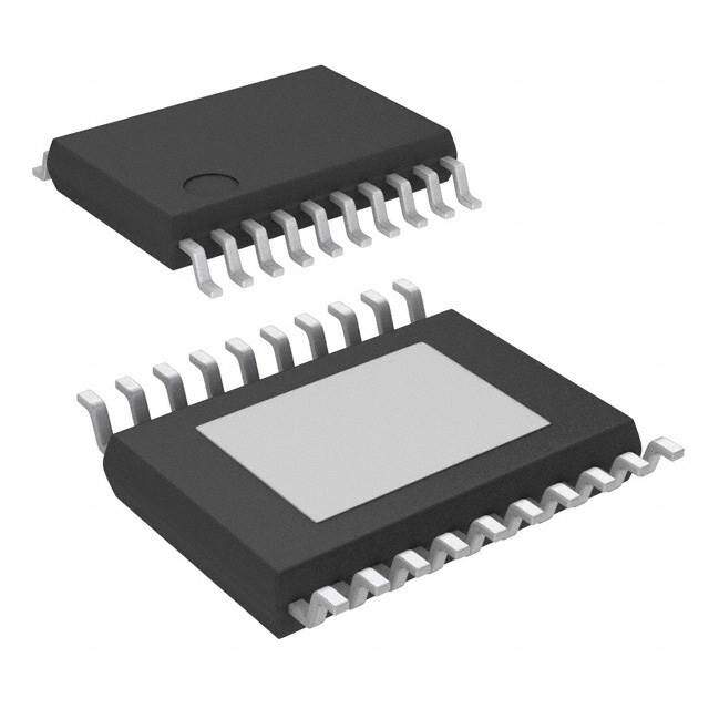
| 描述 | IC OPAMP GP 10MHZ 20HTSSOP运算放大器 - 运放 Quad High-Output |
| 产品分类 | Linear - Amplifiers - Instrumentation, OP Amps, Buffer Amps集成电路 - IC |
| 品牌 | Texas Instruments |
| 产品手册 | |
| 产品图片 |
|
| rohs | 符合RoHS无铅 / 符合限制有害物质指令(RoHS)规范要求 |
| 产品系列 | 放大器 IC,运算放大器 - 运放,Texas Instruments TLC085AIPWP- |
| 数据手册 | |
| 产品型号 | TLC085AIPWP |
| 产品目录页面 | |
| 产品种类 | 运算放大器 - 运放 |
| 供应商器件封装 | 20-HTSSOP |
| 共模抑制比—最小值 | 80 dB |
| 关闭 | Shutdown |
| 其它名称 | 296-7291-5 |
| 包装 | 管件 |
| 单位重量 | 81.800 mg |
| 压摆率 | 19 V/µs |
| 双重电源电压 | +/- 3 V, +/- 5 V |
| 商标 | Texas Instruments |
| 增益带宽生成 | 10 MHz |
| 增益带宽积 | 10MHz |
| 安装类型 | 表面贴装 |
| 安装风格 | SMD/SMT |
| 封装 | Tube |
| 封装/外壳 | 20-TSSOP(0.173",4.40mm 宽)裸焊盘 |
| 封装/箱体 | HTSSOP-20 |
| 工作温度 | -40°C ~ 125°C |
| 工作电源电压 | 4.5 V to 16 V, +/- 2.25 V to +/- 8 V |
| 工厂包装数量 | 70 |
| 技术 | BiCMOS |
| 放大器类型 | 通用 |
| 最大双重电源电压 | +/- 8 V |
| 最大工作温度 | + 125 C |
| 最小双重电源电压 | +/- 2.25 V |
| 最小工作温度 | - 40 C |
| 标准包装 | 70 |
| 电压-电源,单/双 (±) | 4.5 V ~ 16 V, ±2.25 V ~ 8 V |
| 电压-输入失调 | 390µV |
| 电流-电源 | 1.9mA |
| 电流-输入偏置 | 2pA |
| 电流-输出/通道 | 57mA |
| 电源电流 | 11.6 mA |
| 电路数 | 4 |
| 系列 | TLC085A |
| 转换速度 | 16 V/us |
| 输入偏压电流—最大 | 50 pA |
| 输入参考电压噪声 | 12 nV |
| 输入补偿电压 | 1.4 mV |
| 输出电流 | 57 mA |
| 输出类型 | - |
| 通道数量 | 4 Channel |


.jpg)


- 商务部:美国ITC正式对集成电路等产品启动337调查
- 曝三星4nm工艺存在良率问题 高通将骁龙8 Gen1或转产台积电
- 太阳诱电将投资9.5亿元在常州建新厂生产MLCC 预计2023年完工
- 英特尔发布欧洲新工厂建设计划 深化IDM 2.0 战略
- 台积电先进制程称霸业界 有大客户加持明年业绩稳了
- 达到5530亿美元!SIA预计今年全球半导体销售额将创下新高
- 英特尔拟将自动驾驶子公司Mobileye上市 估值或超500亿美元
- 三星加码芯片和SET,合并消费电子和移动部门,撤换高东真等 CEO
- 三星电子宣布重大人事变动 还合并消费电子和移动部门
- 海关总署:前11个月进口集成电路产品价值2.52万亿元 增长14.8%


PDF Datasheet 数据手册内容提取
TLC080 , TLC081, TLC082 TLC083, TLC084, TLC085, TLC08xA www.ti.com SLOS254F–JUNE1999–REVISEDDECEMBER2011 FAMILY OF WIDE-BANDWIDTH HIGH-OUTPUT-DRIVE SINGLE SUPPLY OPERATIONAL AMPLIFIERS CheckforSamples:TLC080,TLC081,TLC082,TLC083,TLC084,TLC085,TLC08xA FEATURES DESCRIPTION 1 • WideBandwidth:10MHz The first members of TI’s new BiMOS 23 general-purpose operational amplifier family are the • HighOutputDrive: TLC08x. The BiMOS family concept is simple: – IOH:57mAatVDD– 1.5V provide an upgrade path for BiFET users who are – I :55mAat0.5V moving away from dual-supply to single-supply OL systems and demand higher ac and dc performance. • HighSlewRate: With performance rated from 4.5 V to 16 V across – SR+:16V/µs commercial (0°C to 70°C) and an extended industrial – SR–:19V/µs temperature range (–40°C to 125°C), BiMOS suits a wide range of audio, automotive, industrial, and • WideSupplyRange:4.5Vto16V instrumentation applications. Familiar features like • SupplyCurrent:1.9mA/Channel offset nulling pins, and new features like MSOP • UltralowPowerShutdownMode: PowerPAD™ packages and shutdown modes, enable higher levels of performance in a variety of – I :125µA/Channel DD applications. • LowInputNoiseVoltage:8.5nV√Hz Developed in TI’s patented LBC3 BiCMOS process, • InputOffsetVoltage:60µV the new BiMOS amplifiers combine a very high input • Ultra-SmallPackages: impedance, low-noise CMOS front end with a – 8-or10-PinMSOP(TLC080/1/2/3) high-drive bipolar output stage, thus providing the optimum performance features of both. AC performance improvements over the TL08x BiFET predecessors include a bandwidth of 10 MHz (an – increase of 300%) and voltage noise of 8.5 nV/√Hz (an improvement of 60%). DC improvements include + an ensured V that includes ground, a factor of 4 ICR reduction in input offset voltage down to 1.5 mV (maximum) in the standard grade, and a power supplyrejectionimprovementofgreaterthan40dBto 130 dB. Added to this list of impressive features is the ability to drive ±50-mA loads comfortably from an ultrasmall-footprint MSOP PowerPAD package, which positions the TLC08x as the ideal high-performance general-purposeoperationalamplifierfamily. FAMILYPACKAGETABLE NO.OF PACKAGETYPES UNIVERSAL DEVICE CHANNELS MSOP PDIP SOIC TSSOP SHUTDOWN EVMBOARD TLC080 1 8 8 8 — Yes TLC081 1 8 8 8 — TLC082 2 8 8 8 — — RefertotheEVM SelectionGuide TLC083 2 10 14 14 — Yes (Lit#SLOU060) TLC084 4 14 14 20 — TLC085 4 16 16 20 Yes 1 Pleasebeawarethatanimportantnoticeconcerningavailability,standardwarranty,anduseincriticalapplicationsofTexas Instrumentssemiconductorproductsanddisclaimerstheretoappearsattheendofthisdatasheet. PowerPADisatrademarkofTexasInstruments. 2 Allothertrademarksarethepropertyoftheirrespectiveowners. 3 PRODUCTIONDATAinformationiscurrentasofpublicationdate. Copyright©1999–2011,TexasInstrumentsIncorporated Products conform to specifications per the terms of the Texas Instruments standard warranty. Production processing does not necessarilyincludetestingofallparameters.
TLC080 , TLC081, TLC082 TLC083, TLC084, TLC085, TLC08xA SLOS254F–JUNE1999–REVISEDDECEMBER2011 www.ti.com TLC080andTLC081AVAILABLEOPTIONS PACKAGEDDEVICES TA SMALLOUTLINE SMALLOUTLINE PLASTICDIP (D)(1) (DGN)(1) SYMBOL (P) TLC080CD TLC080CDGN xxTIACW TLC080CP 0°Cto70°C TLC081CD TLC081CDGN xxTIACY TLC081CP TLC080ID TLC080IDGN xxTIACX TLC080IP TLC081ID TLC081IDGN xxTIACZ TLC081IP –40°Cto125°C TLC080AID — — TLC080AIP TLC081AID — — TLC081AIP (1) Thispackageisavailabletapedandreeled.Toorderthispackagingoption,addanRsuffixtothepartnumber(e.g.,TLC080CDR). TLC082andTLC083AVAILABLEOPTIONS PACKAGEDDEVICES T SMALL MSOP PLASTIC PLASTIC A OUTLINE DIP DIP (D)(1) (DGN)(1) SYMBOL(2) (DGQ)(1) SYMBOL(2) (N) (P) TLC082CD TLC082CDGN xxTIADZ — — — TLC082CP 0°Cto70°C TLC083CD — — TLC083CDGQ xxTIAEB TLC083CN — TLC082ID TLC082IDGN xxTIAEA — — — TLC082IP TLC083ID — — TLC083IDGQ xxTIAEC TLC083IN — –40°Cto125°C TLC082AID — — — — — TLC082AIP TLC083AID — — — — TLC083AIN — (1) Thispackageisavailabletapedandreeled.Toorderthispackagingoption,addanRsuffixtothepartnumber(e.g.,TLC082CDR). (2) xxrepresentsthedevicedatecode. TLC084andTLC085AVAILABLEOPTIONS PACKAGEDDEVICES TA SMALLOUTLINE PLASTICDIP TSSOP (D)(1) (N) (PWP)(1) TLC084CD TLC084CN TLC084CPWP 0°Cto70°C TLC085CD TLC085CN TLC085CPWP TLC084ID TLC084IN TLC084IPWP TLC085ID TLC085IN TLC085IPWP –40°Cto125°C TLC084AID TLC084AIN TLC084AIPWP TLC085AID TLC085AIN TLC085AIPWP (1) Thispackageisavailabletapedandreeled.Toorderthispackagingoption,addanRsuffixtothepartnumber(e.g.,TLC084CDR). space For the most current package and ordering information, see the Package Option Addendum at the end of this datasheet,orseetheTIwebsiteatwww.ti.com. 2 SubmitDocumentationFeedback Copyright©1999–2011,TexasInstrumentsIncorporated ProductFolderLink(s):TLC080 TLC081 TLC082 TLC083 TLC084 TLC085 TLC08xA
TLC080 , TLC081, TLC082 TLC083, TLC084, TLC085, TLC08xA www.ti.com SLOS254F–JUNE1999–REVISEDDECEMBER2011 TLC080 TLC081 TLC082 D,DGN,ORPPACKAGE D,DGN,ORPPACKAGE D,DGN,ORPPACKAGE (TOPVIEW) (TOPVIEW) (TOPVIEW) NULL 1 8 SHDN NULL 1 8 NC 1OUT 1 8 VDD IN 2 7 VDD IN 2 7 VDD 1IN 2 7 2OUT IN+ 3 6 OUT IN+ 3 6 OUT 1IN+ 3 6 2IN GND 4 5 NULL GND 4 5 NULL GND 4 5 2IN+ TLC083 TLC084 TLC083 DORNPACKAGE DORNPACKAGE DGQPACKAGE (TOPVIEW) (TOPVIEW) (TOPVIEW) 1OUT 1 10 VDD 1OUT 1 14 VDD 1OUT 1 14 4OUT 1IN 2 9 2OUT 1IN 2 13 2OUT 1IN 2 13 4IN 1IN+ 3 8 2IN 1IN+ 3 12 2IN 1IN+ 3 12 4IN+ GND 4 7 2IN+ GND 4 11 2IN+ VDD 4 11 GND 1SHDN 5 6 2SHDN NC 5 10 NC 2IN+ 5 10 3IN+ 1SHDN 6 9 2SHDN 2IN 6 9 3IN NC 7 8 NC 2OUT 7 8 3OUT TLC084 TLC085 TLC085 PWPPACKAGE DORNPACKAGE PWPPACKAGE (TOPVIEW) (TOPVIEW) (TOPVIEW) 1OUT 1 20 4OUT 1OUT 1 16 4OUT 1OUT 1 20 4OUT 1IN 2 19 4IN 1IN 2 15 4IN 1IN 2 19 4IN 1IN+ 3 18 4IN+ 1IN+ 3 14 4IN+ 1IN+ 3 18 4IN+ VDD 4 17 GND VDD 4 13 GND VDD 4 17 GND 2IN+ 5 16 3IN+ 2IN+ 5 12 3IN+ 2IN+ 5 16 3IN+ 2IN 6 15 3IN 2IN 6 11 3IN 2IN 6 15 3IN 2OUT 7 14 3OUT 2OUT 7 10 3OUT 2OUT 7 14 3OUT NC 8 13 NC 1/2SHDN 8 9 3/4SHDN 1/2SHDN 8 13 3/4SHDN NC 9 12 NC NC 9 12 NC NC 10 11 NC NC 10 11 NC NC-Nointernalconnection TYPICALPIN1INDICATORS Pin 1 Printedor Pin 1 Pin 1 Pin 1 Molded Dot Stripe Bevel Edges Molded”U”Shape Copyright©1999–2011,TexasInstrumentsIncorporated SubmitDocumentationFeedback 3 ProductFolderLink(s):TLC080 TLC081 TLC082 TLC083 TLC084 TLC085 TLC08xA
TLC080 , TLC081, TLC082 TLC083, TLC084, TLC085, TLC08xA SLOS254F–JUNE1999–REVISEDDECEMBER2011 www.ti.com ABSOLUTE MAXIMUM RATINGS overoperatingfree-airtemperaturerange(unlessotherwisenoted)(1) VALUE UNIT Supplyvoltage,V (2) 17 V DD Differentialinputvoltagerange,V ±VDD ID Continuoustotalpowerdissipation SeeDissipationRatingTable Csuffix 0to70 °C Operatingfree-airtemperaturerange,T : A Isuffix −40to125 °C Maximumjunctiontemperature,T 150 °C J Storagetemperaturerange,T –65to150 °C stg Leadtemperature1,6mm(1/16inch)fromcasefor10seconds 260 °C (1) Stressesbeyondthoselistedunder“absolutemaximumratings”maycausepermanentdamagetothedevice.Thesearestressratings only,andfunctionaloperationofthedeviceattheseoranyotherconditionsbeyondthoseindicatedunder“recommendedoperating conditions”isnotimplied.Exposuretoabsolute-maximum-ratedconditionsforextendedperiodsmayaffectdevicereliability. (2) Allvoltagevalues,exceptdifferentialvoltages,arewithrespecttoGND. DISSIPATION RATING TABLE θ θ T ≤25°C PACKAGE JC JA A (°C/W) (°C/W) POWERRATING D(8) 38.3 176 710mW D(14) 26.9 122.3 1022mW D(16) 25.7 114.7 1090mW DGN(8) 4.7 52.7 2.37W DGQ(10) 4.7 52.3 2.39W N(14,16) 32 78 1600mW P(8) 41 104 1200mW PWP(20) 1.40 26.1 4.79W RECOMMENDED OPERATING CONDITIONS MIN MAX UNIT Singlesupply 4.5 16 Supplyvoltage,V V DD Splitsupply ±2.25 ±8 Common-modeinputvoltage,V GND V –2 V ICR DD V 2 Shutdownon/offvoltagelevel(1) IH V V 0.8 IL C-suffix 0 70 Operatingfree-airtemperature,T °C A I-suffix –40 125 (1) RelativetothevoltageontheGNDterminalofthedevice. 4 SubmitDocumentationFeedback Copyright©1999–2011,TexasInstrumentsIncorporated ProductFolderLink(s):TLC080 TLC081 TLC082 TLC083 TLC084 TLC085 TLC08xA
TLC080 , TLC081, TLC082 TLC083, TLC084, TLC085, TLC08xA www.ti.com SLOS254F–JUNE1999–REVISEDDECEMBER2011 ELECTRICAL CHARACTERISTICS atspecifiedfree-airtemperature,V =5V(unlessotherwisenoted) DD PARAMETER TESTCONDITIONS TA(1) MIN TYP MAX UNIT TLC080/1/2/3, 25°C 390 1900 TLC084/5 Fullrange 3000 VIO Inputoffsetvoltage VDD=5V, TLC080/1/2/3A, 25°C 390 1400 µV V =2.5V, IC V =2.5V, TLC084/5A Fullrange 2000 O Temperaturecoefficientof R =50Ω ∝V S 1.2 µV/°C IO inputoffsetvoltage 25°C 1.9 50 I Inputoffsetcurrent V =5V, TLC08XC 100 pA IO DD Fullrange V =2.5V, TLC08XI 700 IC V =2.5V, 25°C 3 50 O I Inputbiascurrent R =50Ω TLC08XC 100 pA IB S Fullrange TLC08XI 700 25°C 0to3.0 0to3.5 V Common-modeinputvoltage R =50Ω V ICR S Fullrange 0to3.0 0to3.5 25°C 4.1 4.3 I =–1mA OH Fullrange 3.9 25°C 3.7 4 I =–20mA OH Fullrange 3.5 VOH High-leveloutputvoltage VIC=2.5V 25°C 3.4 3.8 V I =–35mA OH Fullrange 3.2 25°C 3.2 3.6 IOH=–50mA –40°Cto 3 85°C 25°C 0.18 0.25 I =1mA OL Fullrange 0.35 25°C 0.35 0.39 I =20mA OL Fullrange 0.45 VOL Low-leveloutputvoltage VIC=2.5V 25°C 0.43 0.55 V I =35mA OL Fullrange 0.7 25°C 0.45 0.63 IOL=50mA –40°Cto 0.7 85°C Sourcing 25°C 100 I Short-circuitoutputcurrent mA OS Sinking 25°C 100 V =1.5Vfrompositiverail 25°C 57 OH I Outputcurrent mA O V =0.5Vfromnegativerail 25°C 55 OL Large-signaldifferential 25°C 100 120 A V =3V, R =10kΩ dB VD voltageamplification O(PP) L Fullrange 100 r Differentialinputresistance 25°C 1000 GΩ i(d) Common-modeinput C f=10kHz 25°C 22.9 pF IC capacitance Closed-loopoutput z f=10kHz, A =10 25°C 0.25 Ω o impedance V 25°C 80 110 CMRR Common-moderejectionratio V =0to3V, R =50Ω dB IC S Fullrange 80 Supplyvoltagerejectionratio VDD=4.5Vto16V, VIC=VDD/2, 25°C 80 100 k dB SVR (ΔVDD/ΔVIO) Noload Fullrange 80 (1) Fullrangeis0°Cto70°CforCsuffixand–40°Cto125°CforIsuffix.Ifnotspecified,fullrangeis–40°Cto125°C. Copyright©1999–2011,TexasInstrumentsIncorporated SubmitDocumentationFeedback 5 ProductFolderLink(s):TLC080 TLC081 TLC082 TLC083 TLC084 TLC085 TLC08xA
TLC080 , TLC081, TLC082 TLC083, TLC084, TLC085, TLC08xA SLOS254F–JUNE1999–REVISEDDECEMBER2011 www.ti.com ELECTRICAL CHARACTERISTICS (continued) atspecifiedfree-airtemperature,V =5V(unlessotherwisenoted) DD PARAMETER TESTCONDITIONS TA(1) MIN TYP MAX UNIT 25°C 1.8 2.5 I Supplycurrent(perchannel) V =2.5V, Noload mA DD O Fullrange 3.5 Supplycurrentinshutdown 25°C 125 200 I mode(perchannel)(TLC080, SHDN≤0.8V µA DD(SHDN) TLC083,TLC085) Fullrange 250 OPERATING CHARACTERISTICS atspecifiedfree-airtemperature,V =5V(unlessotherwisenoted) DD PARAMETER TESTCONDITIONS T (1) MIN TYP MAX UNIT A Positiveslewrateatunity VO(PP)=0.8V, CL=50pF, 25°C 10 16 SR+ V/µs gain R =10kΩ Fullrange 9.5 L Negativeslewrateatunity VO(PP)=0.8V, CL=50pF, 25°C 12.5 19 SR– V/µs gain R =10kΩ Fullrange 10 L Equivalentinputnoise f=100Hz 25°C 12 V nV/√Hz n voltage f=1kHz 25°C 8.5 Equivalentinputnoise I f=1kHz 25°C 0.6 fA/√Hz n current V =3V, A =1 0.002 O(PP) V Totalharmonicdistortion THD+N R =10kΩand250Ω, A =10 25°C 0.012 % plusnoise L V f=1kHz A =100 0.085 V t Amplifierturnontime(2) 25°C 0.15 µs (on) R =10kΩ t Amplifierturnofftime(2) L 25°C 1.3 µs (off) Gain-bandwidthproduct f=10kHz, R =10kΩ 25°C 10 MHz L V =1V, 0.1% 0.18 (STEP)PP A =−1, V CL=10pF, 0.01% 0.39 R =10kΩ L t Settlingtime 25°C µs s V =1V, 0.1% 0.18 (STEP)PP A =–1, V CL=47pF, 0.01% 0.39 R =10kΩ L R =10kΩ, C =50pF 32 L L φ Phasemargin 25°C ° m R =10kΩ, C =0pF 40 L L R =10kΩ, C =50pF 2.2 L L Gainmargin 25°C dB R =10kΩ, C =0pF 3.3 L L (1) Fullrangeis0°Cto70°CforCsuffixand–40°Cto125°CforIsuffix.Ifnotspecified,fullrangeis–40°Cto125°C. (2) DisabletimeandenabletimearedefinedastheintervalbetweenapplicationofthelogicsignaltoSHDNandthepointatwhichthe supplycurrenthasreachedhalfitsfinalvalue. 6 SubmitDocumentationFeedback Copyright©1999–2011,TexasInstrumentsIncorporated ProductFolderLink(s):TLC080 TLC081 TLC082 TLC083 TLC084 TLC085 TLC08xA
TLC080 , TLC081, TLC082 TLC083, TLC084, TLC085, TLC08xA www.ti.com SLOS254F–JUNE1999–REVISEDDECEMBER2011 ELECTRICAL CHARACTERISTICS atspecifiedfree-airtemperature,V =12V(unlessotherwisenoted) DD PARAMETER TESTCONDITIONS TA(1) MIN TYP MAX UNIT TLC080/1/2/3, 25°C 390 1900 TLC084/5 Fullrange 3000 VIO Inputoffsetvoltage VDD=12V, TLC080/1/2/3A, 25°C 390 1400 µV V =6V, IC V =6V, TLC084/5A Fullrange 2000 O Temperaturecoefficientof R =50Ω ∝V S 1.2 µV/°C IO inputoffsetvoltage 25°C 1.5 50 I Inputoffsetcurrent V =12V, TLC08xC 100 pA IO DD Fullrange V =6V, TLC08xI 700 IC V =6V, 25°C 3 50 O I Inputbiascurrent R =50Ω TLC08xC 100 pA IB S Fullrange TLC08xI 700 25°C 0to10.0 0to10.5 V Common-modeinputvoltage R =50Ω V ICR S Fullrange 0to10.0 0to10.5 25°C 11.1 11.2 I =–1mA OH Fullrange 11 25°C 10.8 11 I =–20mA OH Fullrange 10.7 VOH High-leveloutputvoltage VIC=6V 25°C 10.6 10.7 V I =–35mA OH Fullrange 10.3 25°C 10.3 10.5 IOH=–50mA –40°Cto 10.2 85°C 25°C 0.17 0.25 I =1mA OL Fullrange 0.35 25°C 0.35 0.45 I =20mA OL Fullrange 0.5 VOL Low-leveloutputvoltage VIC=6V 25°C 0.4 0.52 V I =35mA OL Fullrange 0.6 25°C 0.45 0.6 IOL=50mA –40°Cto 0.65 85°C Sourcing 25°C 150 I Short-circuitoutputcurrent mA OS Sinking 25°C 150 V =1.5Vfrompositiverail 25°C 57 OH I Outputcurrent mA O V =0.5Vfromnegativerail 25°C 55 OL Large-signaldifferential 25°C 120 140 A V =8V, R =10kΩ dB VD voltageamplification O(PP) L Fullrange 120 r Differentialinputresistance 25°C 1000 GΩ i(d) Common-modeinput C f=10kHz 25°C 21.6 pF IC capacitance Closed-loopoutput z f=10kHz, A =10 25°C 0.25 Ω o impedance V 25°C 80 110 CMRR Common-moderejectionratio V =0to10V, R =50Ω dB IC S Fullrange 80 Supplyvoltagerejectionratio VDD=4.5Vto16V, VIC=VDD/2, 25°C 80 100 k dB SVR (ΔVDD/ΔVIO) Noload Fullrange 80 (1) Fullrangeis0°Cto70°CforCsuffixand–40°Cto125°CforIsuffix.Ifnotspecified,fullrangeis–40°Cto125°C. Copyright©1999–2011,TexasInstrumentsIncorporated SubmitDocumentationFeedback 7 ProductFolderLink(s):TLC080 TLC081 TLC082 TLC083 TLC084 TLC085 TLC08xA
TLC080 , TLC081, TLC082 TLC083, TLC084, TLC085, TLC08xA SLOS254F–JUNE1999–REVISEDDECEMBER2011 www.ti.com ELECTRICAL CHARACTERISTICS (continued) atspecifiedfree-airtemperature,V =12V(unlessotherwisenoted) DD PARAMETER TESTCONDITIONS TA(1) MIN TYP MAX UNIT 25°C 1.9 2.9 I Supplycurrent(perchannel) V =7.5V, Noload mA DD O Fullrange 3.5 Supplycurrentinshutdown 25°C 125 200 I mode(TLC080,TLC083, SHDN≤0.8V µA DD(SHDN) TLC085)(perchannel) Fullrange 250 OPERATING CHARACTERISTICS atspecifiedfree-airtemperature,V =12V(unlessotherwisenoted) DD PARAMETER TESTCONDITIONS T (1) MIN TYP MAX UNIT A Positiveslewrateatunity VO(PP)=2V, CL=50pF, 25°C 10 16 SR+ V/µs gain R =10kΩ Fullrange 9.5 L Negativeslewrateatunity VO(PP)=2V, CL=50pF, 25°C 12.5 19 SR– V/µs gain R =10kΩ Fullrange 10 L Equivalentinputnoise f=100Hz 25°C 14 V nV/√Hz n voltage f=1kHz 25°C 8.5 Equivalentinputnoise I f=1kHz 25°C 0.6 fA/√Hz n current V =8V, A =1 0.002 O(PP) V Totalharmonicdistortion THD+N R =10kΩand250Ω, A =10 25°C 0.005 % plusnoise L V f=1kHz A =100 0.022 V t Amplifierturnontime(2) 25°C 0.47 µs (on) R =10kΩ t Amplifierturnofftime(2) L 25°C 2.5 µs (off) Gain-bandwidthproduct f=10kHz, R =10kΩ 25°C 10 MHz L V =1V, 0.1% 0.17 (STEP)PP A =−1, V CL=10pF, 0.01% 0.22 R =10kΩ L t Settlingtime 25°C µs s V =1V, 0.1% 0.17 (STEP)PP A =–1, V CL=47pF, 0.01% 0.29 R =10kΩ L R =10kΩ, C =50pF 37 L L φ Phasemargin 25°C ° m R =10kΩ, C =0pF 42 L L R =10kΩ, C =50pF 3.1 L L Gainmargin 25°C dB R =10kΩ, C =0pF 4 L L (1) Fullrangeis0°Cto70°CforCsuffixand–40°Cto125°CforIsuffix.Ifnotspecified,fullrangeis–40°Cto125°C. (2) DisabletimeandenabletimearedefinedastheintervalbetweenapplicationofthelogicsignaltoSHDNandthepointatwhichthe supplycurrenthasreachedhalfitsfinalvalue. 8 SubmitDocumentationFeedback Copyright©1999–2011,TexasInstrumentsIncorporated ProductFolderLink(s):TLC080 TLC081 TLC082 TLC083 TLC084 TLC085 TLC08xA
TLC080 , TLC081, TLC082 TLC083, TLC084, TLC085, TLC08xA www.ti.com SLOS254F–JUNE1999–REVISEDDECEMBER2011 TYPICAL CHARACTERISTICS TableofGraphs FIGURE V Inputoffsetvoltage vsCommon-modeinputvoltage 1,2 IO I Inputoffsetcurrent vsFree-airtemperature 3,4 IO I Inputbiascurrent vsFree-airtemperature 3,4 IB V High-leveloutputvoltage vsHigh-leveloutputcurrent 5,7 OH V Low-leveloutputvoltage vsLow-leveloutputcurrent 6,8 OL Z Outputimpedance vsFrequency 9 o I Supplycurrent vsSupplyvoltage 10 DD PSRR Powersupplyrejectionratio vsFrequency 11 CMRR Common-moderejectionratio vsFrequency 12 V Equivalentinputnoisevoltage vsFrequency 13 n V Peak-to-peakoutputvoltage vsFrequency 14,15 O(PP) Crosstalk vsFrequency 16 Differentialvoltagegain vsFrequency 17,18 Phase vsFrequency 17,18 φ Phasemargin vsLoadcapacitance 19,20 m Gainmargin vsLoadcapacitance 21,22 Gain-bandwidthproduct vsSupplyvoltage 23 vsSupplyvoltage 24 SR Slewrate vsFree-airtemperature 25,26 vsFrequency 27,28 THD+N Totalharmonicdistortionplusnoise vsPeak-to-peakoutputvoltage 29,30 Large-signalfollowerpulseresponse 31,32 Small-signalfollowerpulseresponse 33 Large-signalinvertingpulseresponse 34,35 Small-signalinvertingpulseresponse 36 Shutdownforwardisolation vsFrequency 37,38 Shutdownreverseisolation vsFrequency 39,40 vsSupplyvoltage 41 Shutdownsupplycurrent vsFree-airtemperature 42 Shutdownpulse 43,44 Copyright©1999–2011,TexasInstrumentsIncorporated SubmitDocumentationFeedback 9 ProductFolderLink(s):TLC080 TLC081 TLC082 TLC083 TLC084 TLC085 TLC08xA
TLC080 , TLC081, TLC082 TLC083, TLC084, TLC085, TLC08xA SLOS254F–JUNE1999–REVISEDDECEMBER2011 www.ti.com TYPICAL CHARACTERISTICS INPUTBIASCURRENTAND INPUTOFFSETVOLTAGE INPUTOFFSETVOLTAGE INPUTOFFSETCURRENT vs vs vs COMMON-MODEINPUTVOLTAGE COMMON-MODEINPUTVOLTAGE FREE-AIRTEMPERATURE 1000 1500 A 300 800 VTADD= 2=5°5CV 1300 VTADD= 2=51°2CV nt–p 250 VDD= 5 V –mV–VVInputOffsoltageetIO--2424600000000000 - mV–InputOffsetVoltageVIO1--311357910000000000000000 Input Bias and Input Offset Curre 211-50505000000 IIB IIO – -6000.0 0.5 1.0 1.5 2.0 2.5 3.0 3.5 4.0 4.5 5.0 -5000 1 2 3 4 5 6 7 8 9 10 11 12 I/IIBIO-100-55-40-25-10 5 20 35 50 65 80 95110125 VICR–Common-Mode Input Voltage–V VICR–Common-Mode Input Voltage–V TA–Free-Air Temperature–°C Figure1. Figure2. Figure3. INPUTBIASCURRENTAND INPUTOFFSETCURRENT HIGH-LEVELOUTPUTVOLTAGE LOW-LEVELOUTPUTVOLTAGE vs vs vs FREE-AIRTEMPERATURE HIGH-LEVELOUTPUTCURRENT LOW-LEVELOUTPUTCURRENT A 5.0 1.0 p 20 Offset Current– --42000 IIO ut Voltage–V 44..05 VDD= 5 V TA= 70°C TA= 25°C ut Voltage–V 0000....6789 VDD= 5 V TA= 125°C –Input Bias and Input ---111--0426800000 VDD= 12V IIB V–High-Level OutpOH 233...505 TA= 40 °C TA= 125°C V–Low-Level OutpOL 00000.....12345 TA= 2T5A°C= 70°C TA= 40 °C O 2.0 0.0 /IBI -160 0 5 10 15 20 25 30 35 40 45 50 0 5 10 15 20 25 30 35 40 45 50 II -55-40-25-10 5 20 35 50 65 80 95110125 IOH- High-Level Output Current - mA IOL–Low-Level Output Current–mA TA–Free-Air Temperature–°C Figure4. Figure5. Figure6. HIGH-LEVELOUTPUTVOLTAGE LOW-LEVELOUTPUTVOLTAGE OUTPUTIMPEDANCE vs vs vs HIGH-LEVELOUTPUTCURRENT LOW-LEVELOUTPUTCURRENT FREQUENCY 12.0 1.0 1000 V TA= 125°C V 0.9 VDD= 5 V and 12 V V–High-Level Output Voltage–OH111111009.....05055 VDD= 1T2 A V= 2T5A°C= 7T0A°C= 40 °C V–Low-Level Output Voltage–OL 00000000........12345678 TVADD= 2=5 1°2C V TAT=A 7=0° 1C2T5A°C=40 °C WZ–Output Impedance–O01.0110010 AAATVVVA==== 111 20050°C 9.0 0.0 0.01 0 5 10 15 20 25 30 35 40 45 50 0 5 10 15 20 25 30 35 40 45 50 100 1k 10k 100k 1M 10M IOH–High-Level Output Current–mA IOL–Low-Level Output Current–mA f–Frequency–Hz Figure7. Figure8. Figure9. 10 SubmitDocumentationFeedback Copyright©1999–2011,TexasInstrumentsIncorporated ProductFolderLink(s):TLC080 TLC081 TLC082 TLC083 TLC084 TLC085 TLC08xA
TLC080 , TLC081, TLC082 TLC083, TLC084, TLC085, TLC08xA www.ti.com SLOS254F–JUNE1999–REVISEDDECEMBER2011 TYPICAL CHARACTERISTICS POWERSUPPLYREJECTION SUPPLYCURRENT RATIO COMMON-MODEREJECTIONRATIO vs vs vs SUPPLYVOLTAGE FREQUENCY FREQUENCY 2.4 B 140 B 140 d d – – VDD= 5 V and 12 V pply Current–mA 1122....6802 TA=40 °C TA=T A25=° C125°C Supply Rejection Ratio 1120680000 VDD= 12 V n-Mode Rejection Ratio 1102680000 TA= 25°C I–SuDD 111...024 ASPVeHrTD=CAN h1=a= n 7Vn0De°ClD –PPower SRR 42000 VDD= 5 V CMRR–Commo 24000 4 5 6 7 8 9 10 11 12 13 14 15 0 10 100 1k 10k 100k 1M 10M 100 1k 10k 100k 1M 10M VDD–Supply Voltage–V f–Frequency–Hz f–Frequency–Hz Figure10. Figure11. Figure12. EQUIVALENTINPUTNOISE PEAK-TO-PEAKOUTPUT PEAK-TO-PEAKOUTPUT VOLTAGE VOLTAGE VOLTAGE vs vs vs FREQUENCY FREQUENCY FREQUENCY Hz 40 –V 12 –V 12 nV/Voltage– 233550 OutputVoltage 108 VDD= 12 V OutputVoltage 108 VDD= 12 V uivalentInputNoise 2110505 VDD= 5 VVDD= 12 V –Peak-to-PeakPP) 246 VTRHDLDD=+ =6N 050< ΩV=5% –Peak-to-PeakPP) 246 TRVHLD=DD +1N0= k5<Ω =V5% Eq O( TA= 25°C O( TA= 25°C – 0 V 0 V 0 Vn 10 100 1k 10k 100k 10k 100k 1M 10M 10k 100k 1M 10M f–Frequency–Hz f–Frequency–H f–Frequency–Hz Figure13. Figure14. Figure15. CROSSTALK vs FREQUENCY 0 VDD=5Vand12V -20 AV= 1 RL= 10 kΩ -40 VI(PP)= 2 V ForAllChannels B -60 d – k -80 al st os -100 Cr -120 -140 -160 10 100 1k 10k 100k f–Frequency–Hz Figure16. Copyright©1999–2011,TexasInstrumentsIncorporated SubmitDocumentationFeedback 11 ProductFolderLink(s):TLC080 TLC081 TLC082 TLC083 TLC084 TLC085 TLC08xA
TLC080 , TLC081, TLC082 TLC083, TLC084, TLC085, TLC08xA SLOS254F–JUNE1999–REVISEDDECEMBER2011 www.ti.com TYPICAL CHARACTERISTICS DIFFERENTIALVOLTAGEGAINAND DIFFERENTIALVOLTAGEGAINAND PHASE PHASE vs vs FREQUENCY FREQUENCY 80 0 80 0 B 70 B 70 d d – 60 Gain -45 – 60 Gain -45 n n Gai 50 Gai 50 DifferentVoltage 24310000 Phase --19305 °–Phase DifferentVoltage 24310000 Phase --19305 °–Phase – – AVD 0 VRDLD= =10± 2kΩ.5 V -180 AVD 0 VRDLD==10±6kΩV -180 -10 CL= 0 pF -10 CL= 0 pFTA TA= 25°C =25°C -20 -225 -20 -225 1k 10k 100k 1M 10M 100M 1k 10k 100k 1M 10M 100M f–Frequency–Hz f–Frequency–Hz Figure17. Figure18. PHASEMARGIN PHASEMARGIN GAINMARGIN vs vs vs LOADCAPACITANCE LOADCAPACITANCE LOADCAPACITANCE 40° 45° 4 Rnull= 0Ω Rnull= 0Ω 35° Rnull= 100Ω 40° Rnull= 0Ω 3.5 30° 35° B 3 Rnull= 100Ω φ–Phase Marginm 12210055°°°° VDD= 5 V Rnull= 50RΩnull= 20Ω φ–Phase Marginm 1232100055°°°°° VRDnuDll== 1120 0VΩ Rnull= 50RΩnull= 20Ω –GGain Margin–d 21..1525 VDD= 5 VRnull= 50Ω 5° RTAL== 1205° kCΩ 5° RTAL== 1205° kCΩ 0.5 RTAL== 1205° kCΩ Rnull= 20Ω 0° 0° 0 10 100 10 100 10 100 CL–Load Capacitance–pF CL–Load Capacitance–pF CL–Load Capacitance–pF Figure19. Figure20. Figure21. GAINMARGIN GAINBANDWIDTHPRODUCT SLEWRATE vs vs vs LOADCAPACITANCE SUPPLYVOLTAGE SUPPLYVOLTAGE 5 10.0 22 4.45 Rnull= 0ΩRnull= 100Ω ct–MHz 99..89 CTLA== 1215 °pCF 2201 RCAVLL=== 651000 pΩFand 10 kΩ φ–Phase Margin–dBm 321...123555 VDRDnu=ll 1=2 5 V0Ω Rnull= 20Ω –Gain Bandwidth Produ 999999......234567 RL= 600Ω RL= 10 kΩ mSR–Sslew Rate–V/ 111111456789 SlewS RleawteRate+ RL= 10 kΩ WP 0.5 TA= 25°C B 9.1 13 G 0 9.0 12 10 100 4 5 6 7 8 9 10 11 12 13 14 15 16 4 5 6 7 8 9 10 111213 14 15 16 CL–Load Capacitance–pF VDD–Supply Voltage–V VDD–Supply Voltage–V Figure22. Figure23. Figure24. 12 SubmitDocumentationFeedback Copyright©1999–2011,TexasInstrumentsIncorporated ProductFolderLink(s):TLC080 TLC081 TLC082 TLC083 TLC084 TLC085 TLC08xA
TLC080 , TLC081, TLC082 TLC083, TLC084, TLC085, TLC08xA www.ti.com SLOS254F–JUNE1999–REVISEDDECEMBER2011 TYPICAL CHARACTERISTICS TOTALHARMONICDISTORTION SLEWRATE SLEWRATE PLUSNOISE vs vs vs FREE-AIRTEMPERATURE FREE-AIRTEMPERATURE FREQUENCY 25 25 1 20 Slew Rate VRCADVLL=D== 6 =5100 05 p ΩVFand 10 kΩ 20 Slew Rate– oise–% VVRDOLD(=P =1P0 )5 =k VΩ2V ms–Slew Rate–V/ 1105 SlewRate+ m–Slsew Rate–V/ 1105 SlewRate+ monic Distortion + N 00.0.11 AAVV==11000 SR 5 SR 5 VRCADVLL=D== 6 =5100 01 p2ΩF Vand 10 kΩ Total Har AV= 1 0 0 0.001 -55 -35 -15 5 25 45 65 85 105 125 -55 -35 -15 5 25 45 65 85 105125 100 1k 10k 100k TA–Free-Air Temperature–°C TA–Free-Air Temperature–°C f–Frequency– Hz Figure25. Figure26. Figure27. TOTALHARMONICDISTORTION TOTALHARMONICDISTORTION TOTALHARMONICDISTORTION PLUSNOISE PLUSNOISE PLUSNOISE vs vs vs FREQUENCY PEAK-TO-PEAKOUTPUTVOLTAGE PEAK-TO-PEAKOUTPUTVOLTAGE 0.1 10 10 monic Distortion + Noise–% 0.01 AAVV== 11000 VVRDOLD(=P =1P0 )1 =k2Ω 8V V monic Distortion + Noise–% 0.00.111 VAf =DV D1= k1=Hz5V RL= 600ΩRL= 250Ω monic Distortion + Noise–% 0.00.111 VAf =DV D1= k=1H1z2V RL= 600RΩL= 250Ω Total Har AV= 1 Total Har 0.001 RL= 10 kΩ Total Har 0.001 RL= 10 kΩ 0.001 0.0001 0.0001 100 1k 10k 100k 0.25 0.75 1.25 1.75 2.25 2.75 3.25 3.75 0.5 2.5 4.5 6.5 8.5 10.5 f–Frequency–Hz VO(PP) –Peak-to-Peak Output Voltage–V VO(PP) –Peak-to-Peak Output Voltage–V Figure28. Figure29. Figure30. LARGESIGNALFOLLOWER LARGESIGNALFOLLOWER SMALLSIGNALFOLLOWER PULSERESPONSE PULSERESPONSE PULSERESPONSE VI(1 V/Div) VI(5 V/Div) VI(100mV/Div) V V V – – – utVoltage VO(500mV/Div) utVoltage VO(2 V/Div) utVoltage utp utp utp VO(50mV/Div) –O VDD= 5 V –O VDD= 12 V –O O RL= 600Ω O RL= 600Ω O V and 10 kΩ V and 10 kΩ V VDD= 5 V and 12 V CL= 8 pF CL= 8 pF RL= 600Ωand 10kΩ TA= 25°C TA= 25°C CTAL== 825 p°FC 0 0.2 0.4 0.6 0.8 1 1.2 1.4 1.6 1.8 2 0 0.2 0.4 0.6 0.8 1 1.2 1.4 1.6 1.8 2 0 0.1 0.2 0.3 0.4 0.5 0.6 0.7 00..8 0.90.10 t–Time–ms t–Time–ms t–Time–ms Figure31. Figure32. Figure33. Copyright©1999–2011,TexasInstrumentsIncorporated SubmitDocumentationFeedback 13 ProductFolderLink(s):TLC080 TLC081 TLC082 TLC083 TLC084 TLC085 TLC08xA
TLC080 , TLC081, TLC082 TLC083, TLC084, TLC085, TLC08xA SLOS254F–JUNE1999–REVISEDDECEMBER2011 www.ti.com TYPICAL CHARACTERISTICS LARGESIGNALINVERTING LARGESIGNALINVERTING SMALLSIGNALINVERTING PULSERESPONSE PULSERESPONSE PULSERESPONSE VI(2 V/div) VI(5 V/div) VI(100 mV/div) V V V – – – –OVutput VoltageO VRCTAaDLLnD===d 2=68150 0p5°0 F CkVΩΩ –OVutput VoltageO VRCTADLLanD===d 2=68 150 p10°0F2C kΩ VΩ V–Output VoltageO VRCTADLLD=== 2=6850 p5°0F CVΩ aanndd 1 120 V kΩ VO(50 mV/Div) VO(500mV/Div) VO(2 V/Div) 0 0.2 0.4 0.6 0.8 1 1.2 1.4 1.6 1.8 2 0 0.2 0.4 0.6 0.8 1 1.2 1.4 1.6 1.8 2 0 0.1 0.2 0.3 0.4 0.5 0.6 0.7 0.8 0.9 1 t–Time–ms t–Time–ms t–Time–ms Figure34. Figure35. Figure36. SHUTDOWNFORWARD SHUTDOWNFORWARD SHUTDOWNREVERSE ISOLATION ISOLATION ISOLATION vs vs vs FREQUENCY FREQUENCY FREQUENCY 140 140 140 wnForwardIsolation–dB 1102680000 VCTVADIL(P=D= P 02R=) 5p L=5°F C=0V .610, 02.Ω5, and 5 V nForwardIsolation–dB 1102680000 RL= 10 kΩ VCTVADILR(P=D=L P 02==) 5 p 6=1°F0 2C00 .V1Ω, 8, 12 V nReverseIsolation–dB 1102680000 VCTVADIL(P=D= P 02=) 5p =5°F C0VR.1L, =2 .650, 0anΩd 5 V do RL= 10 kΩ ow ow RL= 10 kΩ Sut 40 utd 40 utd 40 S S 20 20 20 100 1k 10k 100k 1M 10M 100M 100 1k 10k 100k 1M 10M 100M 100 1k 10k 100k 1M 10M 100M f–Frequency–Hz f–Frequency–Hz f–Frequency–Hz Figure37. Figure38. Figure39. SHUTDOWNREVERSE ISOLATION SHUTDOWNSUPPLYCURRENT SHUTDOWNSUPPLYCURRENT vs vs vs FREQUENCY SUPPLYVOLTAGE FREE-AIRTEMPERATURE 140 A 136 A 180 SutdownReverseIsolation–dB 110246800000 RL= 10 kΩ VCTVADIL(P=D=R P 0L2=) 5p ==1°F 2C60 0.V10, Ω8, 12 V m–Shutdown Supply Current–HDN)111111112222233302468024 SRVhILNu=t=d o oVpwDennDO/2n m–Shutdown Supply Current–HDN)11110246800000 AVVVIND=D= 1 =V D12D /V2 VDD= 5 V S S 20 DD(118 DD( 60 100 1k 10k 100k 1M 10M 100M I 4 5 6 7 8 9 10 1112 13 14 15 16 I –55 –25 5 35 65 95 125 f–Frequency–Hz VDD–Supply Voltage–V TA–Free-Air Temperature–°C Figure40. Figure41. Figure42. 14 SubmitDocumentationFeedback Copyright©1999–2011,TexasInstrumentsIncorporated ProductFolderLink(s):TLC080 TLC081 TLC082 TLC083 TLC084 TLC085 TLC08xA
TLC080 , TLC081, TLC082 TLC083, TLC084, TLC085, TLC08xA www.ti.com SLOS254F–JUNE1999–REVISEDDECEMBER2011 TYPICAL CHARACTERISTICS SHUTDOWNPULSE SHUTDOWNPULSE 6.0 6 6.0 6 5.5 SD Off 5.5 SDOff mA 45..50 ShutdownPulse 4 mA 45..50 ShutdownPulse 4 I–Supply Current–DD 1122334.......0505050 VCTIDIADDLD=DD= R82=R L5p L5°F= C=V 6 1000 kΩΩ --2024 ShutdownPulse-V I–Supply Current–DD 1122334.......0505050 VCTIDIADDLD=DD= R82=R L5p L1°F=2C= 6 V1000 kΩΩ --2024 ShutdownPulse-V 0.5 0.5 0.0 -6 0.0 -6 0 10 20 30 40 50 60 70 80 0 10 20 30 40 50 60 70 80 t–Time–ms t–Time–ms Figure43. Figure44. PARAMETER MEASUREMENT INFORMATION _ Rnull + RL CL Figure 45 Figure45. APPLICATION INFORMATION Input Offset Voltage Null Circuit TheTLC080andTLC081hasaninputoffsetnullingfunction.RefertoFigure46forthediagram. IN OUT N2 IN+ + N1 100kΩ R1 VDD A. R1=5.6kΩforoffsetvoltageadjustmentof±10mV.R1=20kΩforoffsetvoltageadjustmentof±3mV. Figure46. InputOffsetVoltageNullCircuit Copyright©1999–2011,TexasInstrumentsIncorporated SubmitDocumentationFeedback 15 ProductFolderLink(s):TLC080 TLC081 TLC082 TLC083 TLC084 TLC085 TLC08xA
TLC080 , TLC081, TLC082 TLC083, TLC084, TLC085, TLC08xA SLOS254F–JUNE1999–REVISEDDECEMBER2011 www.ti.com Driving a Capacitive Load When the amplifier is configured in this manner, capacitive loading directly on the output will decrease the device’s phase margin leading to high frequency ringing or oscillations. Therefore, for capacitive loads of greater than 10 pF, it is recommended that a resistor be placed in series (R ) with the output of the amplifier, as NULL showninFigure47.Aminimumvalueof20 Ω shouldworkwellformostapplications. RF RG Input _ RNULL Output + CLOAD Figure47. DrivingaCapacitiveLoad Offset Voltage Theoutputoffsetvoltage,(V )isthesumoftheinputoffsetvoltage(V )andbothinputbiascurrents(I )times OO IO IB thecorrespondinggains.Thefollowingschematicandformulacanbeusedtocalculatetheoutputoffsetvoltage: RF IIB– RG + VI VO + RS IIB+ ( ( )) ( ( )) RF RF VOO = VIO 1+ R ±IIB+ RS 1+ R ±IIB–RF G G Figure48. OutputOffsetVoltageModel 16 SubmitDocumentationFeedback Copyright©1999–2011,TexasInstrumentsIncorporated ProductFolderLink(s):TLC080 TLC081 TLC082 TLC083 TLC084 TLC085 TLC08xA
TLC080 , TLC081, TLC082 TLC083, TLC084, TLC085, TLC08xA www.ti.com SLOS254F–JUNE1999–REVISEDDECEMBER2011 High Speed CMOS Input Amplifiers The TLC08x is a family of high-speed low-noise CMOS input operational amplifiers that has an input capacitance oftheorderof20pF.Anyresistorusedinthefeedbackpathaddsapoleinthetransferfunctionequivalenttothe input capacitance multiplied by the combination of source resistance and feedback resistance. For example, a gain of –10, a source resistance of 1 kΩ, and a feedback resistance of 10 kΩ add an additional pole at approximately 8 MHz. This is more apparent with CMOS amplifiers than bipolar amplifiers due to their greater inputcapacitance. This is of little consequence on slower CMOS amplifiers, as this pole normally occurs at frequencies above their unity-gain bandwidth. However, the TLC08x with its 10-MHz bandwidth means that this pole normally occurs at frequencieswherethereisontheorderof5dBgainleftandthephaseshiftaddsconsiderably. The effect of this pole is the strongest with large feedback resistances at small closed loop gains. As the feedback resistance is increased, the gain peaking increases at a lower frequency and the 180° phase shift crossoverpointalsomovesdowninfrequency,decreasingthephasemargin. For the TLC08x, the maximum feedback resistor recommended is 5 kΩ; larger resistances can be used but a capacitor in parallel with the feedback resistor is recommended to counter the effects of the input capacitance pole. The TLC083 with a 1-V step response has an 80% overshoot with a natural frequency of 3.5 MHz when configured as a unity gain buffer and with a 10-kΩ feedback resistor. By adding a 10-pF capacitor in parallel with the feedback resistor, the overshoot is reduced to 40% and eliminates the natural frequency, resulting in a much fastersettlingtime(seeFigure49).The10-pFcapacitorwaschosenforconvenienceonly. Load capacitance had little effect on these measurements due to the excellent output drive capability of the TLC08x. V 2 – VIN ge 10 pF 1 olta V With 0 put 10 kΩ –V 1.5 CF= 10 pF 1 –In e VI _ g Volta 1 IN + –Output 0.50 VOUT VARRDVFLD=== =6+1001±0 5kΩΩV 50Ω 600Ω 22 pF O CL= 22 pF V 0.5 0 0.2 0.4 0.6 0.8 1 1.2 1.4 1.6 t - Time -ms Figure49. 1-VStepResponse Copyright©1999–2011,TexasInstrumentsIncorporated SubmitDocumentationFeedback 17 ProductFolderLink(s):TLC080 TLC081 TLC082 TLC083 TLC084 TLC085 TLC08xA
TLC080 , TLC081, TLC082 TLC083, TLC084, TLC085, TLC08xA SLOS254F–JUNE1999–REVISEDDECEMBER2011 www.ti.com General Configurations When receiving low-level signals, limiting the bandwidth of the incoming signals into theFigure 50 system is often required. The simplest way to accomplish this is to place an RC filter at the noninverting terminal of the amplifier (see). RG RF + VO VI R1 C1 1 f–3dB = 2pR1C1 ( )( ) V R O F 1 VI = 1+ RG 1 + sR1C1 Figure50. Single-PoleLow-PassFilter If even more attenuation is needed, a multiple pole filter is required. The Sallen-Key filter can be used for this task. For best results, the amplifier should have a bandwidth that is 8 to 10 times the filter frequency bandwidth. Failuretodothiscanresultinphaseshiftoftheamplifier. C1 R1=R2=R C1 = C2 = C Q = Peaking Factor (Butterworth Q = 0.707) VI + R1 R2 _ f–3dB = 2p1RC C2 RF RG = ( ) RF 2 – 1 RG Q Figure51. 2-PoleLow-PassSallen-KeyFilter 18 SubmitDocumentationFeedback Copyright©1999–2011,TexasInstrumentsIncorporated ProductFolderLink(s):TLC080 TLC081 TLC082 TLC083 TLC084 TLC085 TLC08xA
TLC080 , TLC081, TLC082 TLC083, TLC084, TLC085, TLC08xA www.ti.com SLOS254F–JUNE1999–REVISEDDECEMBER2011 Shutdown Function Three members of the TLC08x family (TLC080/3/5) have a shutdown terminal (SHDN) for conserving battery life in portable applications. When the shutdown terminal is tied low, the supply current is reduced to 125 µA/channel, the amplifier is disabled, and the outputs are placed in a high-impedance mode. To enable the amplifier, the shutdown terminal can either be left floating or pulled high. When the shutdown terminal is left floating, care should be taken to ensure that parasitic leakage current at the shutdown terminal does not inadvertently place the operational amplifier into shutdown. The shutdown terminal threshold is always referenced to the voltage on the GND terminal of the device. Therefore, when operating the device with split supply voltages (e.g. ±2.5 V), the shutdown terminal needs to be pulled to V (not system ground) to disable DD– theoperationalamplifier. The amplifier’s output with a shutdown pulse is shown in Figure 43 and Figure 44. The amplifier is powered with a single 5-V supply and is configured as noninverting with a gain of 5. The amplifier turnon and turnoff times are measured from the 50% point of the shutdown pulse to the 50% point of the output waveform. The times for the single,dual,andquadarelistedinthedatatables. Figure 37 through Figure 40 show the amplifiers forward and reverse isolation in shutdown. The operational amplifier is configured as a voltage follower (A = 1). The isolation performance is plotted across frequency using V 0.1 V , 2.5 V , and 5 V input signals at ±2.5 V supplies and 0.1 V , 8 V , and 12 V input signals at ±6 V PP PP PP PP PP PP supplies. Circuit Layout Considerations To achieve the levels of high performance of the TLC08x, follow proper printed-circuit board design techniques. Ageneralsetofguidelinesisgiveninthefollowing. • Ground planes – It is highly recommended that a ground plane be used on the board to provide all components with a low inductive ground connection. However, in the areas of the amplifier inputs and output, thegroundplanecanberemovedtominimizethestraycapacitance. • Properpowersupplydecoupling–Usea6.8-µFtantalumcapacitorinparallelwitha0.1-µFceramiccapacitor on each supply terminal. It may be possible to share the tantalum among several amplifiers depending on the application, but a 0.1-µF ceramic capacitor should always be used on the supply terminal of every amplifier. Inaddition,the0.1-µFcapacitorshouldbeplacedascloseaspossibletothesupplyterminal.Asthisdistance increases, the inductance in the connecting trace makes the capacitor less effective. The designer should strivefordistancesoflessthan0.1inchesbetweenthedevicepowerterminalsandtheceramiccapacitors. • Sockets – Sockets can be used but are not recommended. The additional lead inductance in the socket pins will often lead to stability problems. Surface-mount packages soldered directly to the printed-circuit board is thebestimplementation. • Short trace runs/compact part placements – Optimum high performance is achieved when stray series inductance has been minimized. To realize this, the circuit layout should be made as compact as possible, thereby minimizing the length of all trace runs. Particular attention should be paid to the inverting input of the amplifier. Its length should be kept as short as possible. This will help to minimize stray capacitance at the inputoftheamplifier. • Surface-mount passive components – Using surface-mount passive components is recommended for high performance amplifier circuits for several reasons. First, because of the extremely low lead inductance of surface-mount components, the problem with stray series inductance is greatly reduced. Second, the small size of surface-mount components naturally leads to a more compact layout thereby minimizing both stray inductance and capacitance. If leaded components are used, it is recommended that the lead lengths be kept asshortaspossible. Copyright©1999–2011,TexasInstrumentsIncorporated SubmitDocumentationFeedback 19 ProductFolderLink(s):TLC080 TLC081 TLC082 TLC083 TLC084 TLC085 TLC08xA
TLC080 , TLC081, TLC082 TLC083, TLC084, TLC085, TLC08xA SLOS254F–JUNE1999–REVISEDDECEMBER2011 www.ti.com General PowerPAD Design Considerations The TLC08x is available in a thermally-enhanced PowerPAD family of packages. These packages are constructed using a downset leadframe upon which the die is mounted [see Figure 52(a) and Figure 52(b)]. This arrangement results in the lead frame being exposed as a thermal pad on the underside of the package [see Figure 52(c)]. Because this thermal pad has direct thermal contact with the die, excellent thermal performance canbeachievedbyprovidingagoodthermalpathawayfromthethermalpad. DIE SideView(a) Thermal Pad DIE Bottom View (c) EndView(b) A. Thethermalpadiselectricallyisolatedfromallterminalsinthepackage. Figure52. ViewsofThermally-EnhancedDGNPackage The PowerPAD package allows for both assembly and thermal management in one manufacturing operation. During the surface-mount solder operation (when the leads are being soldered), the thermal pad must be soldered to a copper area underneath the package. Through the use of thermal paths within this copper area, heat can be conducted away from the package into either a ground plane or other heat dissipating device. Soldering the PowerPAD to the printed circuit board (PCB) is always required, even with applications that have low power dissipation. This soldering provides the necessary thermal and mechanical connection betweentheleadframediepadandthePCB. Although there are many ways to properly heatsink the PowerPAD package, the following steps illustrate the recommendedapproach. 20 SubmitDocumentationFeedback Copyright©1999–2011,TexasInstrumentsIncorporated ProductFolderLink(s):TLC080 TLC081 TLC082 TLC083 TLC084 TLC085 TLC08xA
TLC080 , TLC081, TLC082 TLC083, TLC084, TLC085, TLC08xA www.ti.com SLOS254F–JUNE1999–REVISEDDECEMBER2011 ThePowerPADmustbeconnectedtothemostnegativesupplyvoltage(GNDpinpotential)ofthedevice. 1. Prepare the PCB with a top side etch pattern (see the landing patterns at the end of this data sheet). There shouldbeetchfortheleadsaswellasetchforthethermalpad. 2. Place five holes (dual) or nine holes (quad) in the area of the thermal pad. These holes should be 13 mils in diameter.Keepthemsmallsothatsolderwickingthroughtheholesisnotaproblemduringreflow. 3. Additional vias may be placed anywhere along the thermal plane outside of the thermal pad area. This helps dissipatetheheatgeneratedbytheTLC08xIC.Theseadditionalviasmaybelargerthanthe13-mildiameter vias directly under the thermal pad. They can be larger because they are not in the thermal pad area to be solderedsothatwickingisnotaproblem. 4. Connectallholestotheinternalplanethatisatthesamepotentialasthegroundpinofthedevice. 5. When connecting these holes to this internal plane, do not use the typical web or spoke via connection methodology. Web connections have a high thermal resistance connection that is useful for slowing the heat transfer during soldering operations. This makes the soldering of vias that have plane connections easier. In this application, however, low thermal resistance is desired for the most efficient heat transfer. Therefore, the holes under the TLC08x PowerPAD package should make their connection to the internal ground plane with acompleteconnectionaroundtheentirecircumferenceoftheplated-throughhole. 6. The top-side solder mask should leave the terminals of the package and the thermal pad area with its five holes (dual) or nine holes (quad) exposed. The bottom-side solder mask should cover the five or nine holes of the thermal pad area. This prevents solder from being pulled away from the thermal pad area during the reflowprocess. 7. ApplysolderpastetotheexposedthermalpadareaandalloftheICterminals. 8. With these preparatory steps in place, the TLC08x IC is simply placed in position and run through the solder reflowoperationasanystandardsurface-mountcomponent.Thisresultsinapartthatisproperlyinstalled. Foragivenθ ,themaximumpowerdissipationisshowninFigure53andiscalculatedbythefollowingformula: JA PD=æçèTMθAJXA-TAö÷ø (1) Where: P = MaximumpowerdissipationofTLC08xIC(watts) D T = Absolutemaximumjunctiontemperature(150°C) MAX T = Free-ambientairtemperature(°C) A θ = θ + θ JA JC CA θ =Thermalcoefficientfromjunctiontocase JC θ =Thermalcoefficientfromcasetoambientair(°C/W) CA Copyright©1999–2011,TexasInstrumentsIncorporated SubmitDocumentationFeedback 21 ProductFolderLink(s):TLC080 TLC081 TLC082 TLC083 TLC084 TLC085 TLC08xA
TLC080 , TLC081, TLC082 TLC083, TLC084, TLC085, TLC08xA SLOS254F–JUNE1999–REVISEDDECEMBER2011 www.ti.com 7 PWPPackage TJ = 150°C Low-KTestPCB 6 θJA= 29.7°C/W W SOT-23Package – Low-KTestPCB on 5 θJA= 324°C/W2 ati DGNPackage p Low-KTestPCB ssi 4 θJA= 52.3°C/W Di SOIC Package er Low-KTestPCB ow 3 θJA= 176°C/W P PDIPPackage m Low-KTestPCB mu 2 θJA= 104°C/W xi a M 1 0 -55 -40 -25 -10 5 20 35 50 65 80 95 110125 T –Free-Air Temperature–°C A A. ResultsarewithnoairflowandusingJEDECStandardLow-KtestPCB. Figure53. MaximumPowerDissipationvsFree-AirTemperature The next consideration is the package constraints. The two sources of heat within an amplifier are quiescent powerandoutputpower.Thedesignershouldneverforgetaboutthequiescentheatgeneratedwithinthedevice, especiallymulti-amplifierdevices.Becausethesedeviceshavelinearoutputstages(ClassA-B),mostoftheheat dissipationisatlowoutputvoltageswithhighoutputcurrents. The other key factor when dealing with power dissipation is how the devices are mounted on the PCB. The PowerPAD devices are extremely useful for heat dissipation. But, the device should always be soldered to a copper plane to fully use the heat dissipation properties of the PowerPAD. The SOIC package, on the other hand,ishighlydependentonhowitismountedonthePCB.Asmoretraceandcopperareaisplacedaroundthe device, θ decreases and the heat dissipation capability increases. The currents and voltages shown in these JA graphs are for the total package. For the dual or quad amplifier packages, the sum of the RMS output currents andvoltagesshouldbeusedtochoosetheproperpackage. 22 SubmitDocumentationFeedback Copyright©1999–2011,TexasInstrumentsIncorporated ProductFolderLink(s):TLC080 TLC081 TLC082 TLC083 TLC084 TLC085 TLC08xA
TLC080 , TLC081, TLC082 TLC083, TLC084, TLC085, TLC08xA www.ti.com SLOS254F–JUNE1999–REVISEDDECEMBER2011 Macromodel Information Macromodel information provided was derived using Microsim Parts™, the model generation software used with Microsim PSpice™. The Boyle macromodel (see (1)) and subcircuit in Figure 54 are generated using the TLC08x typical electrical and operating characteristics at T = 25°C. Using this information, output simulations of the A followingkeyparameterscanbegeneratedtoatoleranceof20%(inmostcases): • Maximumpositiveoutputvoltageswing • Maximumnegativeoutputvoltageswing • Slewrate • Quiescentpowerdissipation • Inputbiascurrent • Open-loopvoltageamplification • Unity-gainfrequency • Common-moderejectionratio • Phasemargin • DCoutputresistance • ACoutputresistance • Short-circuitoutputcurrentlimit (1) G.R.Boyle,B.M.Cohn,D.O.Pederson,andJ.E.Solomon,“MacromodelingofIntegratedCircuitOperationalAmplifiers,”IEEE JournalofSolid-StateCircuits,SC-9,353(1974). Copyright©1999–2011,TexasInstrumentsIncorporated SubmitDocumentationFeedback 23 ProductFolderLink(s):TLC080 TLC081 TLC082 TLC083 TLC084 TLC085 TLC08xA
TLC080 , TLC081, TLC082 TLC083, TLC084, TLC085, TLC08xA SLOS254F–JUNE1999–REVISEDDECEMBER2011 www.ti.com Figure54. BoyleMacromodelandSubcircuit 24 SubmitDocumentationFeedback Copyright©1999–2011,TexasInstrumentsIncorporated ProductFolderLink(s):TLC080 TLC081 TLC082 TLC083 TLC084 TLC085 TLC08xA
TLC080 , TLC081, TLC082 TLC083, TLC084, TLC085, TLC08xA www.ti.com SLOS254F–JUNE1999–REVISEDDECEMBER2011 REVISION HISTORY NOTE:Pagenumbersforpreviousrevisionsmaydifferfrompagenumbersinthecurrentversion. ChangesfromRevisionE(April2006)toRevisionF Page • UpdatedFigure9 ................................................................................................................................................................ 10 Copyright©1999–2011,TexasInstrumentsIncorporated SubmitDocumentationFeedback 25 ProductFolderLink(s):TLC080 TLC081 TLC082 TLC083 TLC084 TLC085 TLC08xA
PACKAGE OPTION ADDENDUM www.ti.com 6-Feb-2020 PACKAGING INFORMATION Orderable Device Status Package Type Package Pins Package Eco Plan Lead/Ball Finish MSL Peak Temp Op Temp (°C) Device Marking Samples (1) Drawing Qty (2) (6) (3) (4/5) TLC080AIDR ACTIVE SOIC D 8 2500 Green (RoHS NIPDAU Level-1-260C-UNLIM -40 to 125 C080AI & no Sb/Br) TLC080AIP ACTIVE PDIP P 8 50 Green (RoHS NIPDAU N / A for Pkg Type -40 to 125 TLC080AI & no Sb/Br) TLC080CD ACTIVE SOIC D 8 75 Green (RoHS NIPDAU Level-1-260C-UNLIM 0 to 70 C080C & no Sb/Br) TLC080CDGNR ACTIVE HVSSOP DGN 8 2500 Green (RoHS NIPDAU Level-1-260C-UNLIM 0 to 70 ACW & no Sb/Br) TLC080CDGNRG4 ACTIVE HVSSOP DGN 8 2500 Green (RoHS NIPDAU Level-1-260C-UNLIM 0 to 70 ACW & no Sb/Br) TLC080CDR ACTIVE SOIC D 8 2500 Green (RoHS NIPDAU Level-1-260C-UNLIM 0 to 70 C080C & no Sb/Br) TLC080ID ACTIVE SOIC D 8 75 Green (RoHS NIPDAU Level-1-260C-UNLIM -40 to 125 C080I & no Sb/Br) TLC080IDGNR ACTIVE HVSSOP DGN 8 2500 Green (RoHS NIPDAU Level-1-260C-UNLIM -40 to 125 ACX & no Sb/Br) TLC080IDR ACTIVE SOIC D 8 2500 Green (RoHS NIPDAU Level-1-260C-UNLIM -40 to 125 C080I & no Sb/Br) TLC080IP ACTIVE PDIP P 8 50 Green (RoHS NIPDAU N / A for Pkg Type -40 to 125 TLC080I & no Sb/Br) TLC081AID ACTIVE SOIC D 8 75 Green (RoHS NIPDAU Level-1-260C-UNLIM -40 to 125 C081AI & no Sb/Br) TLC081AIDR ACTIVE SOIC D 8 2500 Green (RoHS NIPDAU Level-1-260C-UNLIM -40 to 125 C081AI & no Sb/Br) TLC081AIP ACTIVE PDIP P 8 50 Green (RoHS NIPDAU N / A for Pkg Type -40 to 125 TLC081AI & no Sb/Br) TLC081CD ACTIVE SOIC D 8 75 Green (RoHS NIPDAU Level-1-260C-UNLIM 0 to 70 C081C & no Sb/Br) TLC081CDGN ACTIVE HVSSOP DGN 8 80 Green (RoHS NIPDAU Level-1-260C-UNLIM 0 to 70 ACY & no Sb/Br) TLC081CDGNR ACTIVE HVSSOP DGN 8 2500 Green (RoHS NIPDAU Level-1-260C-UNLIM 0 to 70 ACY & no Sb/Br) TLC081CDR ACTIVE SOIC D 8 2500 Green (RoHS NIPDAU Level-1-260C-UNLIM 0 to 70 C081C & no Sb/Br) Addendum-Page 1
PACKAGE OPTION ADDENDUM www.ti.com 6-Feb-2020 Orderable Device Status Package Type Package Pins Package Eco Plan Lead/Ball Finish MSL Peak Temp Op Temp (°C) Device Marking Samples (1) Drawing Qty (2) (6) (3) (4/5) TLC081CP ACTIVE PDIP P 8 50 Green (RoHS NIPDAU N / A for Pkg Type 0 to 70 TLC081C & no Sb/Br) TLC081ID ACTIVE SOIC D 8 75 Green (RoHS NIPDAU Level-1-260C-UNLIM -40 to 125 C081I & no Sb/Br) TLC081IDGNR ACTIVE HVSSOP DGN 8 2500 Green (RoHS NIPDAU Level-1-260C-UNLIM -40 to 125 ACZ & no Sb/Br) TLC081IDR ACTIVE SOIC D 8 2500 Green (RoHS NIPDAU Level-1-260C-UNLIM -40 to 125 C081I & no Sb/Br) TLC081IDRG4 ACTIVE SOIC D 8 2500 Green (RoHS NIPDAU Level-1-260C-UNLIM -40 to 125 C081I & no Sb/Br) TLC081IP ACTIVE PDIP P 8 50 Green (RoHS NIPDAU N / A for Pkg Type -40 to 125 TLC081I & no Sb/Br) TLC082AID ACTIVE SOIC D 8 75 Green (RoHS NIPDAU Level-1-260C-UNLIM -40 to 125 C082AI & no Sb/Br) TLC082AIDR ACTIVE SOIC D 8 2500 Green (RoHS NIPDAU Level-1-260C-UNLIM -40 to 125 C082AI & no Sb/Br) TLC082AIDRG4 ACTIVE SOIC D 8 2500 Green (RoHS NIPDAU Level-1-260C-UNLIM -40 to 125 C082AI & no Sb/Br) TLC082AIP ACTIVE PDIP P 8 50 Green (RoHS NIPDAU N / A for Pkg Type -40 to 125 C082AI & no Sb/Br) TLC082CD ACTIVE SOIC D 8 75 Green (RoHS NIPDAU Level-1-260C-UNLIM 0 to 70 C082C & no Sb/Br) TLC082CDG4 ACTIVE SOIC D 8 75 Green (RoHS NIPDAU Level-1-260C-UNLIM 0 to 70 C082C & no Sb/Br) TLC082CDGN ACTIVE HVSSOP DGN 8 80 Green (RoHS NIPDAU Level-1-260C-UNLIM 0 to 70 ADZ & no Sb/Br) TLC082CDGNG4 ACTIVE HVSSOP DGN 8 80 Green (RoHS NIPDAU Level-1-260C-UNLIM 0 to 70 ADZ & no Sb/Br) TLC082CDGNR ACTIVE HVSSOP DGN 8 2500 Green (RoHS NIPDAU Level-1-260C-UNLIM 0 to 70 ADZ & no Sb/Br) TLC082CDR ACTIVE SOIC D 8 2500 Green (RoHS NIPDAU Level-1-260C-UNLIM 0 to 70 C082C & no Sb/Br) TLC082CP ACTIVE PDIP P 8 50 Green (RoHS NIPDAU N / A for Pkg Type 0 to 70 C082C & no Sb/Br) TLC082ID ACTIVE SOIC D 8 75 Green (RoHS NIPDAU Level-1-260C-UNLIM -40 to 125 C082I & no Sb/Br) Addendum-Page 2
PACKAGE OPTION ADDENDUM www.ti.com 6-Feb-2020 Orderable Device Status Package Type Package Pins Package Eco Plan Lead/Ball Finish MSL Peak Temp Op Temp (°C) Device Marking Samples (1) Drawing Qty (2) (6) (3) (4/5) TLC082IDGN ACTIVE HVSSOP DGN 8 80 Green (RoHS NIPDAU Level-1-260C-UNLIM -40 to 125 AEA & no Sb/Br) TLC082IDGNR ACTIVE HVSSOP DGN 8 2500 Green (RoHS NIPDAU Level-1-260C-UNLIM -40 to 125 AEA & no Sb/Br) TLC082IDR ACTIVE SOIC D 8 2500 Green (RoHS NIPDAU Level-1-260C-UNLIM -40 to 125 C082I & no Sb/Br) TLC082IDRG4 ACTIVE SOIC D 8 2500 Green (RoHS NIPDAU Level-1-260C-UNLIM -40 to 125 C082I & no Sb/Br) TLC082IP ACTIVE PDIP P 8 50 Green (RoHS NIPDAU N / A for Pkg Type -40 to 125 C082I & no Sb/Br) TLC083AID ACTIVE SOIC D 14 50 Green (RoHS NIPDAU Level-1-260C-UNLIM -40 to 125 C083AI & no Sb/Br) TLC083CDGQR ACTIVE HVSSOP DGQ 10 2500 Green (RoHS NIPDAU Level-1-260C-UNLIM 0 to 70 AEB & no Sb/Br) TLC083CDR ACTIVE SOIC D 14 2500 Green (RoHS NIPDAU Level-1-260C-UNLIM 0 to 70 C083C & no Sb/Br) TLC083CN ACTIVE PDIP N 14 25 Green (RoHS NIPDAU N / A for Pkg Type 0 to 70 C083C & no Sb/Br) TLC083IDGQ ACTIVE HVSSOP DGQ 10 80 Green (RoHS NIPDAU Level-1-260C-UNLIM -40 to 125 AEC & no Sb/Br) TLC083IN ACTIVE PDIP N 14 25 Green (RoHS NIPDAU N / A for Pkg Type -40 to 125 C083I & no Sb/Br) TLC084AID ACTIVE SOIC D 14 50 Green (RoHS NIPDAU Level-1-260C-UNLIM -40 to 125 TLC084AI & no Sb/Br) TLC084AIDG4 ACTIVE SOIC D 14 50 Green (RoHS NIPDAU Level-1-260C-UNLIM -40 to 125 TLC084AI & no Sb/Br) TLC084AIDR ACTIVE SOIC D 14 2500 Green (RoHS NIPDAU Level-1-260C-UNLIM -40 to 125 TLC084AI & no Sb/Br) TLC084AIN ACTIVE PDIP N 14 25 Green (RoHS NIPDAU N / A for Pkg Type -40 to 125 TLC084AI & no Sb/Br) TLC084AIPWP ACTIVE HTSSOP PWP 20 70 Green (RoHS NIPDAU Level-2-260C-1 YEAR -40 to 125 TLC084AI & no Sb/Br) TLC084AIPWPR ACTIVE HTSSOP PWP 20 2000 Green (RoHS NIPDAU Level-2-260C-1 YEAR -40 to 125 TLC084AI & no Sb/Br) TLC084CD ACTIVE SOIC D 14 50 Green (RoHS NIPDAU Level-1-260C-UNLIM 0 to 70 TLC084C & no Sb/Br) Addendum-Page 3
PACKAGE OPTION ADDENDUM www.ti.com 6-Feb-2020 Orderable Device Status Package Type Package Pins Package Eco Plan Lead/Ball Finish MSL Peak Temp Op Temp (°C) Device Marking Samples (1) Drawing Qty (2) (6) (3) (4/5) TLC084CDR ACTIVE SOIC D 14 2500 Green (RoHS NIPDAU Level-1-260C-UNLIM 0 to 70 TLC084C & no Sb/Br) TLC084CN ACTIVE PDIP N 14 25 Green (RoHS NIPDAU N / A for Pkg Type 0 to 70 TLC084C & no Sb/Br) TLC084CNE4 ACTIVE PDIP N 14 25 Green (RoHS NIPDAU N / A for Pkg Type 0 to 70 TLC084C & no Sb/Br) TLC084CPWP ACTIVE HTSSOP PWP 20 70 Green (RoHS NIPDAU Level-2-260C-1 YEAR 0 to 70 TLC084C & no Sb/Br) TLC084CPWPR ACTIVE HTSSOP PWP 20 2000 Green (RoHS NIPDAU Level-2-260C-1 YEAR 0 to 70 TLC084C & no Sb/Br) TLC084ID ACTIVE SOIC D 14 50 Green (RoHS NIPDAU Level-1-260C-UNLIM -40 to 125 TLC084I & no Sb/Br) TLC084IDR ACTIVE SOIC D 14 2500 Green (RoHS NIPDAU Level-1-260C-UNLIM -40 to 125 TLC084I & no Sb/Br) TLC084IDRG4 ACTIVE SOIC D 14 2500 Green (RoHS NIPDAU Level-1-260C-UNLIM -40 to 125 TLC084I & no Sb/Br) TLC084IPWP ACTIVE HTSSOP PWP 20 70 Green (RoHS NIPDAU Level-2-260C-1 YEAR -40 to 125 TLC084I & no Sb/Br) TLC084IPWPR ACTIVE HTSSOP PWP 20 2000 Green (RoHS NIPDAU Level-2-260C-1 YEAR -40 to 125 TLC084I & no Sb/Br) TLC085AID ACTIVE SOIC D 16 40 Green (RoHS NIPDAU Level-1-260C-UNLIM -40 to 125 TLC085AI & no Sb/Br) TLC085AIDR ACTIVE SOIC D 16 2500 Green (RoHS NIPDAU Level-1-260C-UNLIM -40 to 125 TLC085AI & no Sb/Br) TLC085AIN ACTIVE PDIP N 16 25 Green (RoHS NIPDAU N / A for Pkg Type -40 to 125 TLC085AI & no Sb/Br) TLC085AIPWP ACTIVE HTSSOP PWP 20 70 Green (RoHS NIPDAU Level-2-260C-1 YEAR -40 to 125 TLC085AI & no Sb/Br) TLC085CN ACTIVE PDIP N 16 25 Green (RoHS NIPDAU N / A for Pkg Type 0 to 70 TLC085C & no Sb/Br) TLC085CPWP ACTIVE HTSSOP PWP 20 70 Green (RoHS NIPDAU Level-2-260C-1 YEAR 0 to 70 TLC085C & no Sb/Br) (1) The marketing status values are defined as follows: ACTIVE: Product device recommended for new designs. LIFEBUY: TI has announced that the device will be discontinued, and a lifetime-buy period is in effect. NRND: Not recommended for new designs. Device is in production to support existing customers, but TI does not recommend using this part in a new design. Addendum-Page 4
PACKAGE OPTION ADDENDUM www.ti.com 6-Feb-2020 PREVIEW: Device has been announced but is not in production. Samples may or may not be available. OBSOLETE: TI has discontinued the production of the device. (2) RoHS: TI defines "RoHS" to mean semiconductor products that are compliant with the current EU RoHS requirements for all 10 RoHS substances, including the requirement that RoHS substance do not exceed 0.1% by weight in homogeneous materials. Where designed to be soldered at high temperatures, "RoHS" products are suitable for use in specified lead-free processes. TI may reference these types of products as "Pb-Free". RoHS Exempt: TI defines "RoHS Exempt" to mean products that contain lead but are compliant with EU RoHS pursuant to a specific EU RoHS exemption. Green: TI defines "Green" to mean the content of Chlorine (Cl) and Bromine (Br) based flame retardants meet JS709B low halogen requirements of <=1000ppm threshold. Antimony trioxide based flame retardants must also meet the <=1000ppm threshold requirement. (3) MSL, Peak Temp. - The Moisture Sensitivity Level rating according to the JEDEC industry standard classifications, and peak solder temperature. (4) There may be additional marking, which relates to the logo, the lot trace code information, or the environmental category on the device. (5) Multiple Device Markings will be inside parentheses. Only one Device Marking contained in parentheses and separated by a "~" will appear on a device. If a line is indented then it is a continuation of the previous line and the two combined represent the entire Device Marking for that device. (6) Lead/Ball Finish - Orderable Devices may have multiple material finish options. Finish options are separated by a vertical ruled line. Lead/Ball Finish values may wrap to two lines if the finish value exceeds the maximum column width. Important Information and Disclaimer:The information provided on this page represents TI's knowledge and belief as of the date that it is provided. TI bases its knowledge and belief on information provided by third parties, and makes no representation or warranty as to the accuracy of such information. Efforts are underway to better integrate information from third parties. TI has taken and continues to take reasonable steps to provide representative and accurate information but may not have conducted destructive testing or chemical analysis on incoming materials and chemicals. TI and TI suppliers consider certain information to be proprietary, and thus CAS numbers and other limited information may not be available for release. In no event shall TI's liability arising out of such information exceed the total purchase price of the TI part(s) at issue in this document sold by TI to Customer on an annual basis. OTHER QUALIFIED VERSIONS OF TLC082, TLC084 : •Automotive: TLC082-Q1, TLC084-Q1 NOTE: Qualified Version Definitions: •Automotive - Q100 devices qualified for high-reliability automotive applications targeting zero defects Addendum-Page 5
PACKAGE MATERIALS INFORMATION www.ti.com 6-Sep-2019 TAPE AND REEL INFORMATION *Alldimensionsarenominal Device Package Package Pins SPQ Reel Reel A0 B0 K0 P1 W Pin1 Type Drawing Diameter Width (mm) (mm) (mm) (mm) (mm) Quadrant (mm) W1(mm) TLC080AIDR SOIC D 8 2500 330.0 12.4 6.4 5.2 2.1 8.0 12.0 Q1 TLC080CDGNR HVSSOP DGN 8 2500 330.0 12.4 5.3 3.4 1.4 8.0 12.0 Q1 TLC080CDR SOIC D 8 2500 330.0 12.4 6.4 5.2 2.1 8.0 12.0 Q1 TLC080IDGNR HVSSOP DGN 8 2500 330.0 12.4 5.3 3.4 1.4 8.0 12.0 Q1 TLC080IDR SOIC D 8 2500 330.0 12.4 6.4 5.2 2.1 8.0 12.0 Q1 TLC081AIDR SOIC D 8 2500 330.0 12.4 6.4 5.2 2.1 8.0 12.0 Q1 TLC081CDGNR HVSSOP DGN 8 2500 330.0 12.4 5.3 3.4 1.4 8.0 12.0 Q1 TLC081CDR SOIC D 8 2500 330.0 12.4 6.4 5.2 2.1 8.0 12.0 Q1 TLC081IDGNR HVSSOP DGN 8 2500 330.0 12.4 5.3 3.4 1.4 8.0 12.0 Q1 TLC081IDR SOIC D 8 2500 330.0 12.4 6.4 5.2 2.1 8.0 12.0 Q1 TLC082AIDR SOIC D 8 2500 330.0 12.4 6.4 5.2 2.1 8.0 12.0 Q1 TLC082CDGNR HVSSOP DGN 8 2500 330.0 12.4 5.3 3.4 1.4 8.0 12.0 Q1 TLC082CDR SOIC D 8 2500 330.0 12.4 6.4 5.2 2.1 8.0 12.0 Q1 TLC082IDGNR HVSSOP DGN 8 2500 330.0 12.4 5.3 3.4 1.4 8.0 12.0 Q1 TLC082IDR SOIC D 8 2500 330.0 12.4 6.4 5.2 2.1 8.0 12.0 Q1 TLC083CDGQR HVSSOP DGQ 10 2500 330.0 12.4 5.3 3.4 1.4 8.0 12.0 Q1 TLC083CDR SOIC D 14 2500 330.0 16.4 6.5 9.0 2.1 8.0 16.0 Q1 TLC084AIPWPR HTSSOP PWP 20 2000 330.0 16.4 6.95 7.1 1.6 8.0 16.0 Q1 PackMaterials-Page1
PACKAGE MATERIALS INFORMATION www.ti.com 6-Sep-2019 Device Package Package Pins SPQ Reel Reel A0 B0 K0 P1 W Pin1 Type Drawing Diameter Width (mm) (mm) (mm) (mm) (mm) Quadrant (mm) W1(mm) TLC084CPWPR HTSSOP PWP 20 2000 330.0 16.4 6.95 7.1 1.6 8.0 16.0 Q1 TLC084IDR SOIC D 14 2500 330.0 16.4 6.5 9.0 2.1 8.0 16.0 Q1 TLC084IPWPR HTSSOP PWP 20 2000 330.0 16.4 6.95 7.1 1.6 8.0 16.0 Q1 TLC085AIDR SOIC D 16 2500 330.0 16.4 6.5 10.3 2.1 8.0 16.0 Q1 *Alldimensionsarenominal Device PackageType PackageDrawing Pins SPQ Length(mm) Width(mm) Height(mm) TLC080AIDR SOIC D 8 2500 340.5 338.1 20.6 TLC080CDGNR HVSSOP DGN 8 2500 358.0 335.0 35.0 TLC080CDR SOIC D 8 2500 340.5 338.1 20.6 TLC080IDGNR HVSSOP DGN 8 2500 358.0 335.0 35.0 TLC080IDR SOIC D 8 2500 340.5 338.1 20.6 TLC081AIDR SOIC D 8 2500 340.5 338.1 20.6 TLC081CDGNR HVSSOP DGN 8 2500 358.0 335.0 35.0 TLC081CDR SOIC D 8 2500 340.5 338.1 20.6 TLC081IDGNR HVSSOP DGN 8 2500 358.0 335.0 35.0 TLC081IDR SOIC D 8 2500 340.5 338.1 20.6 TLC082AIDR SOIC D 8 2500 340.5 338.1 20.6 TLC082CDGNR HVSSOP DGN 8 2500 358.0 335.0 35.0 TLC082CDR SOIC D 8 2500 340.5 338.1 20.6 PackMaterials-Page2
PACKAGE MATERIALS INFORMATION www.ti.com 6-Sep-2019 Device PackageType PackageDrawing Pins SPQ Length(mm) Width(mm) Height(mm) TLC082IDGNR HVSSOP DGN 8 2500 358.0 335.0 35.0 TLC082IDR SOIC D 8 2500 340.5 338.1 20.6 TLC083CDGQR HVSSOP DGQ 10 2500 358.0 335.0 35.0 TLC083CDR SOIC D 14 2500 350.0 350.0 43.0 TLC084AIPWPR HTSSOP PWP 20 2000 350.0 350.0 43.0 TLC084CPWPR HTSSOP PWP 20 2000 350.0 350.0 43.0 TLC084IDR SOIC D 14 2500 367.0 367.0 38.0 TLC084IPWPR HTSSOP PWP 20 2000 350.0 350.0 43.0 TLC085AIDR SOIC D 16 2500 350.0 350.0 43.0 PackMaterials-Page3
None
None
None
None
PACKAGE OUTLINE D0008A SOIC - 1.75 mm max height SCALE 2.800 SMALL OUTLINE INTEGRATED CIRCUIT C SEATING PLANE .228-.244 TYP [5.80-6.19] .004 [0.1] C A PIN 1 ID AREA 6X .050 [1.27] 8 1 2X .189-.197 [4.81-5.00] .150 NOTE 3 [3.81] 4X (0 -15 ) 4 5 8X .012-.020 B .150-.157 [0.31-0.51] .069 MAX [3.81-3.98] .010 [0.25] C A B [1.75] NOTE 4 .005-.010 TYP [0.13-0.25] 4X (0 -15 ) SEE DETAIL A .010 [0.25] .004-.010 0 - 8 [0.11-0.25] .016-.050 [0.41-1.27] DETAIL A (.041) TYPICAL [1.04] 4214825/C 02/2019 NOTES: 1. Linear dimensions are in inches [millimeters]. Dimensions in parenthesis are for reference only. Controlling dimensions are in inches. Dimensioning and tolerancing per ASME Y14.5M. 2. This drawing is subject to change without notice. 3. This dimension does not include mold flash, protrusions, or gate burrs. Mold flash, protrusions, or gate burrs shall not exceed .006 [0.15] per side. 4. This dimension does not include interlead flash. 5. Reference JEDEC registration MS-012, variation AA. www.ti.com
EXAMPLE BOARD LAYOUT D0008A SOIC - 1.75 mm max height SMALL OUTLINE INTEGRATED CIRCUIT 8X (.061 ) [1.55] SYMM SEE DETAILS 1 8 8X (.024) [0.6] SYMM (R.002 ) TYP [0.05] 5 4 6X (.050 ) [1.27] (.213) [5.4] LAND PATTERN EXAMPLE EXPOSED METAL SHOWN SCALE:8X SOLDER MASK SOLDER MASK METAL OPENING OPENING METAL UNDER SOLDER MASK EXPOSED METAL EXPOSED METAL .0028 MAX .0028 MIN [0.07] [0.07] ALL AROUND ALL AROUND NON SOLDER MASK SOLDER MASK DEFINED DEFINED SOLDER MASK DETAILS 4214825/C 02/2019 NOTES: (continued) 6. Publication IPC-7351 may have alternate designs. 7. Solder mask tolerances between and around signal pads can vary based on board fabrication site. www.ti.com
EXAMPLE STENCIL DESIGN D0008A SOIC - 1.75 mm max height SMALL OUTLINE INTEGRATED CIRCUIT 8X (.061 ) [1.55] SYMM 1 8 8X (.024) [0.6] SYMM (R.002 ) TYP [0.05] 5 4 6X (.050 ) [1.27] (.213) [5.4] SOLDER PASTE EXAMPLE BASED ON .005 INCH [0.125 MM] THICK STENCIL SCALE:8X 4214825/C 02/2019 NOTES: (continued) 8. Laser cutting apertures with trapezoidal walls and rounded corners may offer better paste release. IPC-7525 may have alternate design recommendations. 9. Board assembly site may have different recommendations for stencil design. www.ti.com
None
None
None
None
None
None
None
None
None
PACKAGE OUTLINE DGN0008D PowerPAD TM VSSOP - 1.1 mm max height SCALE 4.000 SMALL OUTLINE PACKAGE C 5.05 A 4.75 TYP 0.1 C PIN 1 INDEX AREA SEATING PLANE 6X 0.65 8 1 2X 3.1 1.95 2.9 NOTE 3 4 5 0.38 8X 0.25 B 3.1 0.13 C A B 2.9 NOTE 4 0.23 0.13 SEE DETAIL A EXPOSED THERMAL PAD 4 5 0.25 GAGE PLANE 1.89 1.63 9 1.1 MAX 8 1 0.7 0.15 0 -8 0.05 0.4 DETA 20AIL A 1.57 TYPICAL 1.28 4225481/A 11/2019 PowerPAD is a trademark of Texas Instruments. NOTES: 1. All linear dimensions are in millimeters. Any dimensions in parenthesis are for reference only. Dimensioning and tolerancing per ASME Y14.5M. 2. This drawing is subject to change without notice. 3. This dimension does not include mold flash, protrusions, or gate burrs. Mold flash, protrusions, or gate burrs shall not exceed 0.15 mm per side. 4. This dimension does not include interlead flash. Interlead flash shall not exceed 0.25 mm per side. 5. Reference JEDEC registration MO-187. www.ti.com
EXAMPLE BOARD LAYOUT DGN0008D PowerPAD TM VSSOP - 1.1 mm max height SMALL OUTLINE PACKAGE (2) NOTE 9 METAL COVERED BY SOLDER MASK (1.57) SYMM SOLDER MASK DEFINED PAD 8X (1.4) (R0.05) TYP 8 8X (0.45) 1 (3) 9 SYMM NOTE 9 (1.89) 6X (0.65) (1.22) 5 4 ( 0.2) TYP VIA (0.55) SEE DETAILS (4.4) LAND PATTERN EXAMPLE EXPOSED METAL SHOWN SCALE: 15X SOLDER MASK METAL METAL UNDER SOLDER MASK OPENING SOLDER MASK OPENING EXPOSED METAL EXPOSED METAL 0.05 MAX 0.05 MIN ALL AROUND ALL AROUND NON-SOLDER MASK SOLDER MASK DEFINED DEFINED (PREFERRED) SOLDE15.000R MASK DETAILS 4225481/A 11/2019 NOTES: (continued) 6. Publication IPC-7351 may have alternate designs. 7. Solder mask tolerances between and around signal pads can vary based on board fabrication site. 8. Vias are optional depending on application, refer to device data sheet. If any vias are implemented, refer to their locations shown on this view. It is recommended that vias under paste be filled, plugged or tented. 9. Size of metal pad may vary due to creepage requirement. www.ti.com
EXAMPLE STENCIL DESIGN DGN0008D PowerPAD TM VSSOP - 1.1 mm max height SMALL OUTLINE PACKAGE (1.57) BASED ON 0.125 THICK STENCIL SYMM 8X (1.4) (R0.05) TYP 8 8X (0.45) 1 (1.89) SYMM BASED ON 0.125 THICK STENCIL 6X (0.65) 4 5 METAL COVERED SEE TABLE FOR BY SOLDER MASK DIFFERENT OPENINGS (4.4) FOR OTHER STENCIL THICKNESSES SOLDER PASTE EXAMPLE EXPOSED PAD 9: 100% PRINTED SOLDER COVERAGE BY AREA SCALE: 15X STENCIL SOLDER STENCIL THICKNESS OPENING 0.1 1.76 X 2.11 0.125 1.57 X 1.89 (SHOWN) 0.15 1.43 X 1.73 0.175 1.33 X 1.60 4225481/A 11/2019 NOTES: (continued) 10. Laser cutting apertures with trapezoidal walls and rounded corners may offer better paste release. IPC-7525 may have alternate design recommendations. 11. Board assembly site may have different recommendations for stencil design. www.ti.com
IMPORTANTNOTICEANDDISCLAIMER TI PROVIDES TECHNICAL AND RELIABILITY DATA (INCLUDING DATASHEETS), DESIGN RESOURCES (INCLUDING REFERENCE DESIGNS), APPLICATION OR OTHER DESIGN ADVICE, WEB TOOLS, SAFETY INFORMATION, AND OTHER RESOURCES “AS IS” AND WITH ALL FAULTS, AND DISCLAIMS ALL WARRANTIES, EXPRESS AND IMPLIED, INCLUDING WITHOUT LIMITATION ANY IMPLIED WARRANTIES OF MERCHANTABILITY, FITNESS FOR A PARTICULAR PURPOSE OR NON-INFRINGEMENT OF THIRD PARTY INTELLECTUAL PROPERTY RIGHTS. These resources are intended for skilled developers designing with TI products. You are solely responsible for (1) selecting the appropriate TI products for your application, (2) designing, validating and testing your application, and (3) ensuring your application meets applicable standards, and any other safety, security, or other requirements. These resources are subject to change without notice. TI grants you permission to use these resources only for development of an application that uses the TI products described in the resource. Other reproduction and display of these resources is prohibited. No license is granted to any other TI intellectual property right or to any third party intellectual property right. TI disclaims responsibility for, and you will fully indemnify TI and its representatives against, any claims, damages, costs, losses, and liabilities arising out of your use of these resources. TI’s products are provided subject to TI’s Terms of Sale (www.ti.com/legal/termsofsale.html) or other applicable terms available either on ti.com or provided in conjunction with such TI products. TI’s provision of these resources does not expand or otherwise alter TI’s applicable warranties or warranty disclaimers for TI products. Mailing Address: Texas Instruments, Post Office Box 655303, Dallas, Texas 75265 Copyright © 2020, Texas Instruments Incorporated