ICGOO在线商城 > 集成电路(IC) > 数据采集 - 模数转换器 > TC7109CPL
 Datasheet下载
- 型号: TC7109CPL
- 制造商: Microchip
- 库位|库存: xxxx|xxxx
- 要求:
| 数量阶梯 | 香港交货 | 国内含税 |
| +xxxx | $xxxx | ¥xxxx |
查看当月历史价格
查看今年历史价格
TC7109CPL产品简介:
ICGOO电子元器件商城为您提供TC7109CPL由Microchip设计生产,在icgoo商城现货销售,并且可以通过原厂、代理商等渠道进行代购。 TC7109CPL价格参考¥41.32-¥41.32。MicrochipTC7109CPL封装/规格:数据采集 - 模数转换器, 12 Bit Analog to Digital Converter 1 Input 1 Dual Slope 40-PDIP。您可以下载TC7109CPL参考资料、Datasheet数据手册功能说明书,资料中有TC7109CPL 详细功能的应用电路图电压和使用方法及教程。
Microchip Technology的TC7109CPL是一款数据采集系统中的模数转换器(ADC),广泛应用于需要高精度、低功耗和小尺寸的场合。以下是其主要应用场景:

 1. 工业自动化与控制
   TC7109CPL适用于各种工业自动化设备,如传感器接口、过程控制系统和智能仪表。它能够将模拟信号(如温度、压力、湿度等)转换为数字信号,供微控制器或处理器处理。由于其低功耗特性,特别适合电池供电的远程传感器节点,延长了系统的运行时间。

 2. 医疗设备
   在医疗领域,TC7109CPL可用于便携式医疗设备,如血糖仪、心率监测仪、血压计等。这些设备要求高精度的信号采集和处理,以确保测量结果的准确性。此外,其低功耗特性有助于延长设备的电池寿命,提升用户体验。

 3. 消费电子
   TC7109CPL可以用于智能家居设备、可穿戴设备和其他消费电子产品中。例如,在智能手表、健康手环等设备中,它可以帮助采集用户的生理参数(如心率、血氧饱和度等),并通过低功耗设计减少对电池的消耗。

 4. 环境监测
   环境监测系统通常需要长时间运行并采集大量数据。TC7109CPL的低功耗和高精度特性使其成为空气质量监测仪、水质检测仪等设备的理想选择。它可以精确地采集环境参数,并通过无线通信模块将数据传输到云端进行分析。

 5. 汽车电子
   在汽车电子领域,TC7109CPL可用于车载传感器系统,如胎压监测、发动机温度监控等。它能够实时采集车辆的各种运行参数,并将其转换为数字信号,供车载计算机进行处理和分析,从而提高驾驶安全性和车辆性能。

 6. 农业与物联网
   在智慧农业中,TC7109CPL可以用于土壤湿度传感器、气象站等设备中,帮助农民实时监控农田环境,优化灌溉和施肥策略。其低功耗特性使得这些设备可以在偏远地区长期稳定运行。

总之,TC7109CPL凭借其高精度、低功耗和小尺寸的优势,广泛应用于多个领域,特别是在需要长时间稳定运行且对精度要求较高的场景中表现出色。
| 参数 | 数值 |
| 产品目录 | 集成电路 (IC)半导体 |
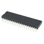
| 描述 | IC ADC 12BIT HANDSHAKE 40DIP模数转换器 - ADC 13 Bit Fast Recovery |
| 产品分类 | |
| 品牌 | Microchip Technology |
| 产品手册 | |
| 产品图片 |
|
| rohs | 符合RoHS无铅 / 符合限制有害物质指令(RoHS)规范要求 |
| 产品系列 | 数据转换器IC,模数转换器 - ADC,Microchip Technology TC7109CPL- |
| 数据手册 | http://www.microchip.com/mymicrochip/filehandler.aspx?ddocname=en011627 |
| 产品型号 | TC7109CPL |
| PCN组件/产地 | http://www.microchip.com/mymicrochip/NotificationDetails.aspx?pcn=CYER-15WDGG555&print=viewhttp://www.microchip.com/mymicrochip/NotificationDetails.aspx?id=5509&print=viewhttp://www.microchip.com/mymicrochip/NotificationDetails.aspx?id=5777&print=view |
| 产品目录页面 | |
| 产品种类 | 模数转换器 - ADC |
| 位数 | 12 |
| 供应商器件封装 | 40-PDIP |
| 信噪比 | No |
| 其它名称 | 158-1059 |
| 分辨率 | 12 bit |
| 包装 | 管件 |
| 商标 | Microchip Technology |
| 安装类型 | 通孔 |
| 安装风格 | Through Hole |
| 封装 | Tube |
| 封装/外壳 | 40-DIP(0.600",15.24mm) |
| 封装/箱体 | PDIP-40 |
| 工作温度 | 0°C ~ 70°C |
| 工作电源电压 | 6.2 V |
| 工厂包装数量 | 10 |
| 接口类型 | Parallel |
| 数据接口 | 串行,并联 |
| 最大功率耗散 | 1230 mW |
| 最大工作温度 | + 70 C |
| 最小工作温度 | 0 C |
| 标准包装 | 10 |
| 电压参考 | Internal, External |
| 电压源 | 双 ± |
| 结构 | Dual-Slope |
| 转换器数 | 1 |
| 转换器数量 | 1 |
| 转换速率 | 0.01 kS/s |
| 输入数和类型 | 1 个差分,单极 |
| 输入类型 | Differential |
| 通道数量 | 1 Channel |
| 采样率(每秒) | - |


- 商务部:美国ITC正式对集成电路等产品启动337调查
- 曝三星4nm工艺存在良率问题 高通将骁龙8 Gen1或转产台积电
- 太阳诱电将投资9.5亿元在常州建新厂生产MLCC 预计2023年完工
- 英特尔发布欧洲新工厂建设计划 深化IDM 2.0 战略
- 台积电先进制程称霸业界 有大客户加持明年业绩稳了
- 达到5530亿美元!SIA预计今年全球半导体销售额将创下新高
- 英特尔拟将自动驾驶子公司Mobileye上市 估值或超500亿美元
- 三星加码芯片和SET,合并消费电子和移动部门,撤换高东真等 CEO
- 三星电子宣布重大人事变动 还合并消费电子和移动部门
- 海关总署:前11个月进口集成电路产品价值2.52万亿元 增长14.8%


PDF Datasheet 数据手册内容提取
TC7109/A µ 12-Bit A-Compatible Analog-to-Digital Converters Features General Description • ZeroIntegratorCycleforFastRecoveryfrom The TC7109A is a 12-bit plus sign, CMOS low power InputOverloads analog-to-digital converter (ADC). Only eight passive (cid:127) EliminatesCross-TalkinMultiplexedSystems components and a crystal are required to form a completedualslopeintegratingADC. (cid:127) 12-BitPlusSignIntegratingA/DConverterwith OverRangeIndication TheimprovedV sourcecurrentandotherTC7109A OH (cid:127) SignMagnitudeCodingFormat featuresmakeitanattractiveper-channelalternativeto analogmultiplexingfor manydataacquisitionapplica- (cid:127) TrueDifferentialSignalInputandDifferential tions.Thesefeaturesincludetypicalinputbiascurrent ReferenceInput of 1pA, drift of less than 1µV/°C, input noise typically (cid:127) LowNoise:15 µV Typ. P-P 15µV ,andauto-zero.Truedifferentialinputandref- P-P (cid:127) InputCurrent:1pATyp. erenceallowmeasurementofbridgetypetransducers, (cid:127) NoZeroAdjustmentneeded such as load cells, strain gauges, and temperature (cid:127) TTLCompatible,ByteOrganizedTri-State transducers. Outputs The TC7109A provides a versatile digital interface. In (cid:127) UARTHandshakeModeforsimpleSerialData the Direct mode, chip select and HIGH/LOW byte Transmissions enablecontrolparallelbusinterface.IntheHandshake mode,theTC7109Awilloperatewithindustrystandard Device Selection Table UARTsincontrollingserialdatatransmission–idealfor remotedatalogging.Controlandmonitoringofconver- PartNumber Temperature sion timing is provided by the RUN/HOLD input and Package (TC7109X)* Range STATUSoutput. TC7109CKW 44-PinPQFP 0°Cto+70°C For applications requiring more resolution, see the TC7109CLW 44-PinPLCC 0°Cto+70°C TC500,15-bitplussignADCdatasheet.TheTC7109A TC7109CPL 40-PinPDIP 0°Cto+70°C has improved over range recovery performance and higheroutputdrivecapabilitythantheoriginalTC7109. TC7109IJL 40-PinCERDIP -25°Cto+85°C All new (or existing) designs should specify the *The“A”versionhasahigherIOUTonthedigitallines. TC7109Awhereverpossible. 2002MicrochipTechnologyInc. DS21456B-page 1
TC7109/A Package Type 44-Pin PQFP 44-Pin PLCC B12 OR POL STATUS GND NC V+ REF IN- REF CAP- REF CAP+ REF IN+ B12 OR POL STATUS GND NC V+ REF IN- REF CAP- REF CAP+ REF IN+ 44 43 42 41 40 39 38 37 36 35 34 6 5 4 3 2 1 44 43 42 41 40 B11 1 33 IN HI B11 7 39IN HI B10 2 32 IN LO B10 8 38IN LO B9 3 31 COMMON B9 9 37COMMON B8 4 30 INT B8 10 36INT B7 5 TC7109ACKW 29 AZ B7 11 TC7109ACLW 35AZ NC 6 TC7109CKW 28 NC NC 12 TC7109CLW 34NC B6 7 27 BUFF B6 13 33BUFF B5 8 26 REF OUT B5 14 32REF OUT B4 9 25 V- B4 15 31V- B3 10 24 SEND B3 16 30SEND B2 11 23 RUN/HOLD B2 17 29RUN/HOLD 12 13 14 15 16 17 18 19 20 21 22 18 19 20 21 22 23 24 25 26 27 28 B1 TEST LBEN HBEN CE/LOAD NC MODE OSC IN OSC OUT OSC SELBUFFOSC OUT B1 TEST LBEN HBEN CE/LOAD NC MODE OSC IN OSC OUT OSC SELBUFFOSC OUT 40-Pin PDIP/CERDIP GND 1 40 V+ STATUS 2 39 REF IN- POL 3 38 REF CAP- OR 4 37 REF CAP+ B12 5 36 REF IN+ B11 6 35 IN HI B10 7 34 IN LO B9 8 TC7109A 33 COMMON B8 9 TC7109 32 INT B7 10 31 AZ B6 11 30 BUFF B5 12 29 REF OUT B4 13 28 V- B3 14 27 SEND B2 15 26 RUN/HOLD B1 16 25 BUFF OSC OUT TEST 17 24 OSC SEL LBEN 18 23 OSC OUT HBEN 19 22 OSC IN CE/LOAD 20 21 MODE NC = No internal connection DS21456B-page 2 2002MicrochipTechnologyInc.
TC7109/A TypicalApplication TC7109A High Order Low Order RCEAFP+ RINE+F CREF RINE-F RCEAFP-RINT BUFF ACZAZ ICNITNT TEST POLORByBt12e InB11puBt10s B9B8B7BB6ytBe5 InB4puBt3s B2B1 37 36 39 38 30 31 32 17 3 4 5 6 7 8 910111213141516 Input 35 INT AZIZ AZZI B+–uffer Inte–grator Comparator 16 Three-State Outputs 112890 LHCBBEEE/LNNOAD High DE DE + Comp (–) (+) Out 14 Latches AZ ZI AZ 12-Bit Counter DE DE Latch Common 33 (+) (–) Clock AZ DE (±) Comp Out Input Low 34 INT ZI 10µA To SAencatlioogn INAZT CCoonntrvoel rLsoiognic COlosccikll aCtoirrc uaintrdy HanLdosghicake DE (±) ZI – + 6.2V 29 28 40 2 26 22 23 24 25 21 27 1 REF V- V+ Status RUN/ OSCOSCOSCBUFFMode Send GND OUT HOLD IN OUTSEL OSC OUT 2002MicrochipTechnologyInc. DS21456B-page 3
TC7109/A 1.0 ELECTRICAL *Stresses above those listed under "Absolute Maximum Ratings"maycausepermanentdamagetothedevice.These CHARACTERISTICS arestressratingsonlyandfunctionaloperationofthedevice attheseoranyotherconditionsabovethoseindicatedinthe Absolute Maximum Ratings* operation sections of the specifications is not implied. Exposure to Absolute Maximum Rating conditions for PositiveSupplyVoltage(GNDtoV+)..................+6.2V extendedperiodsmayaffectdevicereliability. NegativeSupplyVoltage(GNDtoV-).....................-9V AnalogInputVoltage(LowtoHigh)(Note1)....V+toV- ReferenceInputVoltage: (LowtoHigh)(Note1).............................V+toV- DigitalInputVoltage: (Pins2-27)(Note2)...........................GND–0.3V PowerDissipation,T <70°C(Note3) A CerDIP........................................................2.29W PlasticDIP..................................................1.23W PLCC..........................................................1.23W PQFP..........................................................1.00W OperatingTemperatureRange PlasticPackage(C).........................0°Cto+70°C CeramicPackage(I).....................-25°Cto+85°C StorageTemperatureRange..............-65°Cto+150°C TC7109/TC7109AELECTRICALSPECIFICATIONS ElectricalCharacteristics:AllparameterswithV+=+5V,V-=-5V,GND=0V,T =+25°C,unlessotherwiseindicated. A Symbol Parameter Min Typ Max Unit TestConditions Analog OverloadRecoveryTime(TC7109A) — 0 1 Measurement Cycle ZeroInputReading -0000 ±0000 +0000 OctalReading V =0V;FullScale=409.6mV 8 8 8 IN RatioMetricReading 3777 3777 4000 OctalReading V =V 8 8 8 IN REF 4000 V =204.8mV 8 REF NL Non-Linearity(MaxDeviation -1 ±0.2 +1 Count FullScale=409.6mVto2.048V fromBestStraightLineFit) OverFullOperating TemperatureRange RolloverError(DifferenceinReadingfor -1 ±0.02 +1 Count FullScale=409.6mVto EqualPositiveandInputsnear 2.048VOverFullOperating (FullScale) TemperatureRange CMRR InputCommonMode — 50 — µV/V V ±1V,V =0V CM IN RejectionRatio FullScale=409.6mV V CommonModeVoltageRange V-+1.5 — V+-1.5 V InputHigh,InputLowand CMR CommonPins e Noise(P-PValueNot — 15 — µV V =0V,FullScale=409.6mV N IN Exceeded95%ofTime) I LeakageCurrentatInput — 1 10 pA V ,AllPackages:+25°C IN IN — 20 100 pA CDevice:0°C≤T ≤+70°C A — 100 250 pA IDevice:-25°C≤T ≤+85°C A TC ZeroReadingDrift — 0.2 1 µV/°C V =0V ZS IN TC ScaleFactorTemperatureCoefficient — 1 5 µV/°C V =408.9mV=>7770 FS IN 8 Reading,ExtRef=0ppm/°C Note 1: Inputvoltagesmayexceedsupplyvoltagesifinputcurrentislimitedto±100µA. 2: ConnectinganydigitalinputsoroutputstovoltagesgreaterthanV+orlessthanGNDmaycausedestructivedevice latchup.Therefore,itisrecommendedthatinputsfromsourcesotherthanthesamepowersupplyshouldnotbeapplied totheTC7109Abeforeitspowersupplyisestablished.Inmultiplesupplysystems,thesupplytothedeviceshouldbe activatedfirst. 3: Thislimitreferstothatofthepackageandwillnotoccurduringnormaloperation. DS21456B-page 4 2002MicrochipTechnologyInc.
TC7109/A TC7109/TC7109AELECTRICALSPECIFICATIONS (CONTINUED) ElectricalCharacteristics:AllparameterswithV+=+5V,V-=-5V,GND=0V,T =+25°C,unlessotherwiseindicated. A Symbol Parameter Min Typ Max Unit TestConditions I+ SupplyCurrent(V+toGND) — 700 1500 µA VIN=0V,CrystalOscillator 3.58MHzTestCircuit I SupplyCurrent(V+toV-) — 700 1500 µA Pins2-21,25,26,27,29Open S V ReferenceOutVoltage -2.4 -2.8 -3.2 V ReferencedtoV+,25kΩ REF BetweenV+andRefOut TC RefOutTemperatureCoefficient — 80 — ppm/°C 25kΩBetweenV+andRefOut REF 0°C≤ T ≤+70°C A Digital V OutputHighVoltage 3.5 4.3 — V TC7109:I =100µA OH OUT I =700µA Pins3-16,18,19,20 OUT TC7109A:I =700µA OUT V OutputLowVoltage — 0.2 0.4 µA I =1.6mA OL OUT OutputLeakageCurrent — ±0.01 ±1 µA Pins3-16HighImpedance ControlI/OPull-upCurrent — 5 — µF Pins18,19,20V =V+–3V OUT ModeInputatGND ControlI/OLoading — — 50 pF HBEN,Pin19;LBEN,Pin18 V InputHighVoltage 2.5 — — V Pins18-21,26,27 IH ReferencedtoGND V InputLowVoltage — — 1 V Pins18-21,26,27 IL ReferencedtoGND InputPull-upCurrent — 5 — µA Pins26,27;V =V+–3V OUT — 25 — µA Pins17,24;V =V+– 3V OUT InputPull-downCurrent — 1 — µA Pins21,V =GND=+3V OUT OscillatorOutputCurrent,High — 1 — mA V –2.5V OUT OscillatorOutputCurrent,Low — 1.5 — mA V –2.5V OUT BufferedOscillatorOutputCurrentHigh — 2 — mA V –2.5V OUT BufferedOscillatorOutputCurrentLow — 5 — mA V –2.5V OUT t ModeInputPulseWidth 60 — — nsec W Note 1: Inputvoltagesmayexceedsupplyvoltagesifinputcurrentislimitedto±100µA. 2: ConnectinganydigitalinputsoroutputstovoltagesgreaterthanV+orlessthanGNDmaycausedestructivedevice latchup.Therefore,itisrecommendedthatinputsfromsourcesotherthanthesamepowersupplyshouldnotbeapplied totheTC7109Abeforeitspowersupplyisestablished.Inmultiplesupplysystems,thesupplytothedeviceshouldbe activatedfirst. 3: Thislimitreferstothatofthepackageandwillnotoccurduringnormaloperation. HANDLINGPRECAUTIONS:ThesedevicesareCMOSandmustbehandledcorrectlytopreventdamage.Package andstoreonlyinconductivefoam,antistatictubes,orotherconductingmaterial.Useproperantistatichandlingpro- cedures.Donotconnectincircuitsunder"power-on"conditions,ashightransientsmaycausepermanentdamage. 2002MicrochipTechnologyInc. DS21456B-page 5
TC7109/A 2.0 PIN DESCRIPTIONS ThedescriptionsofthepinsarelistedinTable2-1. TABLE2-1: PINFUNCTIONTABLE PinNumber Symbol Description (40-PinPDIP) 1 GND Digitalground,0V,groundreturnforalldigitallogic. 2 STATUS OutputHIGHduringintegrateandde-integrateuntildataislatched.OutputLOWwhen analogsectionisinauto-zeroorzerointegratorconfiguration. 3 POL Polarity-Highforpositiveinput. 4 OR OverRange-Highifoverranged(Three-StateDatabit). 5 B Bit12(MostSignificantbit)(Three-StateDatabit). 12 6 B Bit11(Three-StateDatabit). 11 7 B Bit10(Three-StateDatabit). 10 8 B Bit9(Three-StateDatabit). 9 9 B Bit8(Three-StateDatabit). 8 10 B Bit7(Three-StateDatabit). 7 11 B Bit6(Three-StateDatabit). 6 12 B Bit5(Three-StateDatabit). 5 13 B Bit4(Three-StateDatabit). 4 14 B Bit3(Three-StateDatabit). 3 15 B Bit2(Three-StateDatabit). 2 16 B Bit1(LeastSignificantbit)(Three-StateDatabit). 1 17 TEST InputHigh-Normaloperation.InputLOW-ForcesallbitoutputsHIGH. Note:Thisinputisusedfortestpurposesonly. 18 LBEN LowByteEnable-withMODE(Pin21)LOW,andCE/LOAD(Pin20)LOW,takingthispin LOWactivatesloworderbyteoutputs,B –B .WithMODE(Pin21)HIGH,thispinservesas 1 8 lowbyteflagoutputusedinHandshakemode.(SeeFigure3-7,Figure3-8,andFigure3-9.) 19 HBEN HighByteEnable-withMODE(Pin21)LOW,andCE/LOAD(Pin20)LOW,takingthispin LOWactivateshighorderbyteoutputs,B –B ,POL,OR.WithMODE(Pin21)HIGH,this 9 12 pinservesashighbyteflagoutputusedinHandshakemode.SeeFigures3-7,3-8,and3-9. 20 CE/LOAD ChipEnable/Load-withMODE(Pin21)LOW,CE/LOADservesasamasteroutputenable. WhenHIGH,B –B ,POL,ORoutputsaredisabled.WhenMODE(Pin21)isHIGH,aload 1 12 strobeisusedinhandshakemode.(SeeFigure3-7,Figure3-8,andFigure3-9.) 21 MODE InputLOW-DirectOutputmodewhereCE/LOAD(Pin20),HBEN(Pin19),andLBEN(Pin 18)actasinputsdirectlycontrollingbyteoutputs. InputPulsedHIGH-Causesimmediate entryintoHandshakemodeandoutputofdataasinFigure3-9. InputHIGH-enablesCE/LOAD(Pin20),HBEN(Pin19),andLBEN(Pin18)asoutputs, HandshakemodewillbeenteredanddataoutputasinFigure3-7andFigure3-9 atconversionscompletion. 22 OSCIN OscillatorInput. 23 OSCOUT OscillatorOutput. 24 OSCSEL OscillatorSelect-InputHIGHconfiguresOSCIN,OSCOUT,BUFFOSCOUTasRC oscillator-clockwillbesamephaseanddutycycleasBUFFOSCOUT.InputLOW configuresOSCIN,OSCOUTforcrystaloscillator-clockfrequencywillbe1/58offrequency atBUFFOSCOUT. 25 BUFFOSCOUT BufferedOscillatorOutput. 26 RUN/HOLD InputHIGH-Conversionscontinuouslyperformedevery8192clockpulses. InputLOW-Conversioninprogresscompleted;converterwillstopinauto-zerosevencounts beforeintegrate. 27 SEND Input-UsedinHandshakemodetoindicateabilityofanexternaldevicetoacceptdata. ConnecttoV+ifnotused. 28 V- AnalogNegativeSupply-Nominally-5VwithrespecttoGND(Pin1). 29 REFOUT ReferenceVoltageOutput-Nominally2.8VdownfromV+(Pin40). DS21456B-page 6 2002MicrochipTechnologyInc.
TC7109/A TABLE2-1: PINFUNCTIONTABLE (CONTINUED) PinNumber Symbol Description (40-PinPDIP) 30 BUFF BufferAmplifierOutput. 31 AZ Auto-ZeroNode-InsidefoilofC . AZ 32 INT IntegratorOutput-OutsidefoilofC . INT 33 COMMON AnalogCommon-Systemisauto-zeroedtoCOMMON. 34 INLO DifferentialInputLowSide. 35 INHI DifferentialInputHighSide. 36 REFIN+ DifferentialReferenceInputPositive. 37 REFCAP+ ReferenceCapacitorPositive. 38 REFCAP- ReferenceCapacitorNegative. 39 REFIN- DifferentialReferenceInputNegative. 40 V+ PositiveSupplyVoltage-Nominally+5VwithrespecttoGND(Pin1). Note: AllDigitallevelsarepositivetrue. 3.0 DETAILED DESCRIPTION 3.1.2 SIGNALINTEGRATE PHASE (AllPinDesignationsReferto40-PinDIP.) Thebufferandintegratorinputsareremovedfromcom- mon and connected to input high and input low. The 3.1 Analog Section auto-zero loop is opened. The auto-zero capacitor is placed in series in the loop to provide an equal and The Typical Application diagram on page 3 shows a opposite compensating offset voltage. The differential block diagram of the analog section of the TC7109A. voltagebetweeninputhighandinputlowisintegrated The circuit will perform conversions at a rate deter- forafixedtimeof2048clockperiods.Attheendofthis mined bytheclock frequency(8192clockperiodsper phase, the polarity of the integrated signal is deter- cycle),whentheRUN/HOLDinput isleftopenorcon- mined. If the input signal has no return to the con- nectedtoV+.Eachmeasurementcycleisdividedinto verter's power supply, input low can be tied to analog four phases, as shown in Figure3-1. They are: common to establish the correct Common mode (1)Auto-Zero(AZ),(2)SignalIntegrate(INT), (3) Ref- voltage. erenceDe-integrate(DE),and(4)ZeroIntegrator(ZI). 3.1.3 DE-INTEGRATEPHASE 3.1.1 AUTO-ZEROPHASE Inputhighisconnectedacrossthepreviouslycharged The buffer and the integrator inputs are disconnected reference capacitor and input low is internally con- frominputhighandinputlowandconnectedtoanalog nected to analog common. Circuitry within the chip common.Thereferencecapacitorischargedtotheref- ensuresthecapacitorwillbeconnectedwiththecorrect erence voltage. A feedback loop is closed aroundthe polarity to cause the integrator output to return to the systemtochargetheauto-zerocapacitor,C ,tocom- AZ zero crossing (established by auto-zero), with a fixed pensate for offset voltage in the buffer amplifier, inte- slope. The time, represented by the number of clock grator, and comparator. Since the comparator is periods counted for the output to return to zero, is includedintheloop,theAZaccuracyislimitedonlyby proportionaltotheinputsignal. thenoiseofthesystem.Theoffsetreferredtotheinput islessthan10µV. 2002MicrochipTechnologyInc. DS21456B-page 7
TC7109/A 3.1.4 ZEROINTEGRATORPHASE 3.1.6 DIFFERENTIALREFERENCE The ZI phase only occurs when an input over range The reference voltage can be generated anywhere conditionexists.ThefunctionoftheZIphaseistoelim- withinthepowersupplyvoltageof theconverter.Roll- inateresidualchargeontheintegratorcapacitorafteran over voltage is the main source of Common mode overrangemeasurement.Unlessremoved,theresidual error,causedbythereferencecapacitorlosingorgain- chargewillbetransferredtotheauto-zerocapacitorand ing charge, due to straycapacityonits nodes. With a causeanerrorinthesucceedingconversion. large Common mode voltage, the reference capacitor cangaincharge(increasevoltage)whencalleduponto TheZIphasevirtuallyeliminateshysteresis,or"cross- de-integrate a positive signal and lose charge talk" in multiplexed systems. An over range input on (decreasevoltage)whencalledupontode-integratea onechannelwillnotcauseanerroronthenextchannel negative input signal. This difference in reference for measured.Thisfeatureisespeciallyuseful inthermo- (+)or(–)inputvoltageswillcausearollovererror.This couplemeasurements,whereunused(orbrokenther- errorcanbeheldtolessthan0.5count,worstcase,by mocouple)inputsarepulledtothepositivesupplyrail. usingalargereferencecapacitorincomparisontothe DuringZI,thereferencecapacitorischargedtotheref- stray capacitance. To minimize rollover error from erence voltage. The signal inputs are disconnected these sources, keep the reference Common mode fromthebufferandintegrator.Thecomparatoroutputis voltagenearoratanalogcommon. connected to the buffer input, causing the integrator output to be driven rapidly to 0V (Figure3-1). The ZI 3.2 Digital Section phaseonlyoccursfollowinganoverrangeandlastsfor amaximumof1024clockperiods. ThedigitalsectionisshowninFigure3-2andincludes the clock oscillator and scaling circuit, a 12-bit binary 3.1.5 DIFFERENTIALINPUT counterwithoutputlatchesandTTLcompatiblethree- state output drivers, UART handshake logic, polarity, The TC7109A has been optimized for operation with overrange,andcontrollogic.Logiclevelsarereferred analogcommonneardigitalground.With+5Vand-5V toasLOWorHIGH. power supplies, a full ±4V full scale integrator swing maximizestheanalogsection'sperformance. InputsdrivenfromTTLgatesshouldhave3kΩto5kΩ pull-up resistors added for maximum noise immunity. AtypicalCMRRof86dBisachievedforinputdifferen- For minimum power consumption, all inputs should tial voltages anywhere within the typical Common swingfromGND(LOW)toV+(HIGH). mode range of 1V below the positive supply, to 1.5V abovethenegativesupply.However,foroptimumper- 3.2.1 STATUSOUTPUT formance,theINHIandINLOinputsshouldnotcome within2Vofeithersupplyrail.Sincetheintegratoralso During a conversion cycle, the STATUS output goes swingswiththeCommonmodevoltage,caremust be highat thebeginningof signalintegrateandgoeslow exercisedtoensuretheintegratoroutputdoesnotsat- one-half clock period after new data from the conver- urate.Aworstcaseconditionisnearafullscalenega- sion has been stored in the output latches (see tive differential input voltage with a large positive Figure3-1). The signal may beused asa "datavalid" Common mode voltage. The negative input signal flag to drive interrupts, or for monitoring the status of drives the integrator positive when most of its swing theconverter.(Datawillnotchangewhilestatusislow.) hasbeenusedupbythepositiveCommonmodevolt- 3.2.2 MODE INPUT age. In such cases, the integrator swing can be reducedtolessthan therecommended±4Vfull scale TheOutputmodeof theconverter iscontrolledbythe value, with some loss of accuracy. Theintegrator out- MODE input. The converter is in its "Direct" Output put can swing to within 0.3V of either supply without mode,whentheMODEinputisLOWorleftopen.The lossoflinearity. output data is directly accessible under the control of thechipand byteenableinputs (thisinput isprovided withapull-downresistor toensure aLOW level when the pin is left open). When the MODE input is pulsed high,theconverterenterstheUARTHandshakemode andoutputsthedatain2bytes,thenreturnsto"Direct" mode. When the MODE input is kept HIGH, the con- verter will output data in the Handshake mode at the endofeveryconversioncycle.WithMODE=0(direct bustransfer),thesendinputshouldbetiedtoV+.(See "HandshakeMode".) DS21456B-page 8 2002MicrochipTechnologyInc.
TC7109/A 3.2.3 RUN/HOLDINPUT periodsafterRUN/HOLDischangedtoHIGH,andthe converter will begin the integrate phase of the next With the RUN/HOLD input high, or open, the circuit conversion. operates normally as a dual slope ADC, as shown in The RUN/HOLD input allows controlled conversion Figure3-1. Conversion cycles operate continuously with the output latches updated after zero crossing in interface. Theconverter maybeheld at IDLEinauto- the De-integrate mode. An internal pull-up resistor is zerowithRUN/HOLDLOW.Theconversionisstarted providedtoensureaHIGHlevelwithanopeninput. when RUN/HOLD goes HIGH, and the new data is validwhentheSTATUSoutputgoesLOW (oristrans- TheRUN/HOLDinputmaybeusedtoshortenconver- ferred to the UART; see "Handshake Mode"). RUN/ siontime.IfRUN/HOLDgoesLOWanytimeafterzero HOLDmaynowgoLOW,terminatingde-integrateand crossingintheDe-integratemode,thecircuitwilljump ensuringaminimumauto-zerotimebeforestoppingto toauto-zeroandeliminatethatportionoftimenormally wait for the next conversion. Conversion time can be spentinde-integrate. minimized by ensuring RUN/HOLD goes LOW during If RUN/HOLD staysor goes LOW, theconversionwill de-integrate,afterzerocrossing,andgoesHIGHafter completewithminimumtimeinde-integrate.Itwillstay theholdpointisreached. inauto-zerofortheminimumtimeandwaitinauto-zero The required activity on the RUN/HOLD input can be for a HIGH at the RUN/HOLD input. As shown in providedbyconnectingittothebufferedoscillatorout- Figure3-3, the STATUS output will go HIGH, 7 clock put.Inthismode,theinputvaluemeasureddetermines theconversiontime. FIGURE3-1: CONVERSIONTIMING(RUN/HOLDPINHIGH Integrator ZI Saturates AZ Zero Integrator Phase forces Integrator Output No Zero Crossing Integrator Output for Over Range Input to 0V Zero Crossing Occurs Zero Crossing Detected Integrator Output for Normal Input AZ INT DE AZ Phase I Phase II Phase III Internal Clock Internal Latch Status Output 2048 Fixed 4096 Counts 2048 Counts Min. Counts Max Number of Counts to Zero Crossing After Zero Crossing, Analog section will Proportional to VIN be in Auto-Zero Configuration 2002MicrochipTechnologyInc. DS21456B-page 9
TC7109/A FIGURE3-2: DIGITALSECTION High Order Low Order Byte Outputs Byte Outputs B B B B B B B B B B B B TEST POLOR 12 11 10 9 8 7 6 5 4 3 2 1 17 3 4 5 6 7 8 9 10 11 12 13 14 15 16 18 LBEN 19 14 Three-State Outputs HBEN 20 CE/LOAD 14 Latches 12-Bit Counter Latch Clock COMP OUT To AZ Conversion Oscillator and Handshake Analog INT Control Logic Clock Circuitry Logic Section DE (±) ZI 2 26 22 23 24 25 21 27 1 STATUS RUN/ OSCOSCOSCBUFF MODE SEND GND HOLD IN OUTSEL OSC OUT FIGURE3-3: TC7109ARUN/HOLDOPERATION Auto-Zero Phase I Min 1790 Counts Determinated at Static in Max 2041 Counts Zero Crossing Hold State Detection INT Phase II Integrator Output 7 Counts Internal Clock Internal Latch Status Output RUN/HOLD Input * *Note: RUN/HOLD input is ignored until end of auto-zero phase. DS21456B-page 10 2002MicrochipTechnologyInc.
TC7109/A 3.2.4 DIRECTMODE 3.2.5 HANDSHAKEMODE Thedataoutputs(bits1through8,loworderbytes;bits An alternative means of interfacing the TC7109A to 9through12,polarityandoverrangehighorderbytes) digital systems is provided when the Handshake Out- are accessible under control of the byte and chip putmodeoftheTC7109Abecomesactiveincontrolling enable terminals as inputs, with the MODE pin at a theflowofdata,insteadofpassivelyrespondingtochip LOW level. These three inputs are all active LOW. andbyteenableinputs.Thismodeallowsadirectinter- Internal pull-up resistors are provided for an inactive face between the TC7109A and industry standard HIGHlevelwhenleftopen.WhenchipenableisLOW, UARTs with no external logic required. The TC7109A a byte enable input LOW will allow the outputs of the provides all the control and flag signals necessary to byte to become active. A variety of parallel data sequencethetwobytesofdataintotheUARTandini- accessing techniques may be used, as shown in the tiate their transmission in serial form when triggered "Interfacing"section.(SeeFigure3-4andTable3-1.) into the Handshake mode. The cost of designing remotedataacquisitionstationsisreducedusingserial The access of data should be synchronized with the data transmission to minimize the number of lines to conversion cycle by monitoring the STATUS output. thecentralcontrollingprocessor. Thispreventsaccessingdatawhileitisbeingupdated andeliminatestheacquisitionoferroneousdata. TheMODEinputcontrolstheHandshakemode.When theMODEinputisheldHIGH,theTC7109Aentersthe FIGURE3-4: TC7109ADIRECTMODE Handshakemodeafternewdatahasbeenstoredinthe OUTPUTTIMING output latches at the end of every conversion per- formed(seeFigure3-7andFigure3-8).Entryintothe tCEA Handshakemodemaybetriggeredondemandbythe CE/LOAD MODEinput.At anytimeduringtheconversioncycle, As Input the LOW-to-HIGH transition of a short pulse at the tBEA MODEinputwillcauseimmediateentryintotheHand- HBEN shake mode. If this pulse occurs while new data is As Input being stored, the entry into Handshake mode is LBEN delayed until the data is stable. The MODE input is As Input ignored in the Handshake mode, and until the con- tDAB tDAB vertercompletestheoutputcycleandclearstheHand- High DBayttea VDaaltiad VDaaltiad shake mode, data updating will be inhibited (see tDAC tDHC Figure3-9). Low Byte Data WhentheMODEinputisHIGH,orwhentheconverter Data Valid enterstheHandshakemode,thechipandbyteenable = High Impedance inputsbecomeTTLcompatibleoutputs,whichprovide the output cycle control signals (see Figure3-7, TABLE 3-1: TC7109ADIRECTMODE Figure3-8andFigure3-9).TheSENDinputisusedby TIMINGREQUIREMENTS the converter as an indication of the ability of the receivingdevice(suchasaUART)toacceptdatainthe Symbol Description Min Typ Max Units Handshake mode. The sequence of the output cycle t ByteEnableWidth 200 500 — nsec with SEND held HIGH is shown in Figure3-7. The BEA t DataAccessTime — 150 300 nsec Handshake mode (internal MODE HIGH) is entered DAB fromByteEnable after the data latch pulse (the CE/LOAD, LBEN and HBEN terminals are active as outputs, since MODE t DataHoldTimefrom — 150 300 nsec DHB ByteEnable remainsHIGH). t ChipEnableWidth 300 500 nsec The HIGH level at the SEND input is sensed on the CEA t DataAccessTime — 200 400 nsec same HIGH-to-LOW internal clock edge. On the next DAC fromChipEnable LOW-to-HIGH internalclockedge,thehighorder byte (bits9through12,POL,andOR)outputsareenabled t DataHoldTimefrom — 200 400 nsec DHC ChipEnable and the CE/LOAD and the HBEN outputs assume a LOWlevel.TheCE/LOADoutputremainsLOWforone full internal clock periodonly; thedataoutputsremain activefor1-1/2internalclockperiods;andthehighbyte enableremainsLOWfor2clockperiods. 2002MicrochipTechnologyInc. DS21456B-page11
TC7109/A The CE/LOAD output LOW level, or LOW-to-HIGH 3.3 Oscillator edge,maybeusedasasynchronizingsignaltoensure Theoscillatormaybeoverdriven,ormaybeoperated valid data, and the byte enable as an output may be usedasabyteidentificationflag.WithSENDremaining as an RC or crystal oscillator. The OSCILLATOR HIGH, theconvertercompletestheoutput cycleusing SELECT input optimizes the internal configuration of CE/LOADandLBEN,whiletheloworderbyteoutputs the oscillator for RC or crystal operation. The OSCIL- LATORSELECTinputisprovidedwithapull-upresis- (bits 1 through 8) are activated. When both bytes are tor.WhentheOSCILLATORSELECTinputisHIGHor sent, the Handshake mode is terminated. The typical leftopen,theoscillatorisconfiguredforRCoperation. UARTinterfacingtimingisshowninFigure3-8. The internal clock will be the same frequency and The SEND input is used to delay portions of the phase asthesignal at the BUFFERED OSCILLATOR sequence,orhandshake,toensurecorrectdatatrans- OUTPUT. Connect the resistor and capacitor as in fer. This timing diagram shows an industry standard Figure3-5.Thecircuitwilloscillateatafrequencygiven HD6403 or CDP1854 CMOS UART to interface to byf = 0.45/RC. A100kΩ resistor isrecommended for serialdatachannels.TheSENDinputtotheTC7109A usefulrangesoffrequency.Thecapacitorvalueshould is driven by the TBRE (Transmitter Buffer Register bechosensuchthat2048clockperiodsareclosetoan Empty)outputoftheUART,andtheCE/LOADinputof integralmultipleofthe60Hz periodfor optimum 60Hz theTC7109AdrivestheTBRL(TransmitterBufferReg- linerejection. ister Load) input to the UART. The eight transmitter buffer register inputs accept the parallel data outputs. FIGURE3-5: TC7109ARC With the UART transmitter buffer register empty, the OSCILLATOR SENDinputwillbeHIGHwhentheHandshakemodeis entered, after newdataisstored.Thehigh order byte outputs become active and the CE/LOAD and HBEN inputs will go LOW after SEND is sensed. When CE/ LOAD goes HIGH at the end of one clock period, the highorderbytedataisclockedintotheUARTtransmit- 24 22 23 25 terbufferregister.TheUARTTBREoutputwillgoLOW, OSC OSC OSC Buffered which halts the output cycle with the HBEN output SEL IN OUT OSC OUT LOW,andthehighorderbyteoutputsactive.Whenthe R UARThastransferredthedatatothetransmitterregis- C ter and cleared the transmitter buffer register, the TBRE returns HIGH. The high order byte outputs are V+ or Open FOSC = 0.45/RC disabledonthenextTC7109AinternalclockHIGH-to- LOWedge,andone-halfinternalclocklater,theHBEN With OSCILLATOR SELECT input LOW, two on-chip outputreturnsHIGH.TheCE/LOADandLBENoutputs capacitors and a feedback device are added to the goLOWatthesametimeastheloworderbyteoutputs oscillator. Inthis configuration, theoscillator will oper- become active. When the CE/LOAD returns HIGH at atewithmostcrystalsinthe1MHzto5MHzrange,with the end of one clock period, the low order data is no external components (Figure3-6). The OSCILLA- clocked into the UART transmitter buffer register, and TORSELECTinputLOWinsertsafixed458dividercir- TBRE again goes LOW. The next TC7109A internal cuitbetweentheBUFFEREDOSCILLATOROUTPUT clock HIGH-to-LOW edge will sense when TBRE and the internal clock. A 3.58MHz TV crystal gives a returns toa HIGH, disablingthedatainputs. One-half divisionratio,providinganintegrationtimegivenby: internal clock later, the Handshake mode is cleared, andtheCE/LOAD,HBEN andLBEN terminalsreturn EQUATION3-1: HIGHandstayactive,ifMODEstillremainsHIGH. 58 t=(2048clockperiods) =33.18msec Handshake output sequences may be performed on 3.58MHz demand by triggering the converter into Handshake modewithaLOW-to-HIGHedgeontheMODEinput.A handshake output sequence triggered is shown in Figure3-9. The SEND input is LOW when the con- verter enters Handshake mode. The whole output sequence is controlled by the SEND input, and the sequenceforthefirst(highorder)byteissimilartothe sequenceforthesecondbyte. Figure3-9 also shows that the output sequence can takelongerthanaconversioncycle.Newdatawillnot be latched when the Handshake mode is still in progressandis,therefore,lost. DS21456B-page 12 2002MicrochipTechnologyInc.
TC7109/A FIGURE3-6: CRYSTALOSCILLATOR The error is less than 1% from two 60Hz periods, or 33.33msec, which will give better than 40dB, 60Hz V+ Clock rejection.Theconverterwilloperatereliablyatconver- sion rates up to30 per second, corresponding to a clockfrequencyof245.8kHz. ÷58 Whentheoscillatoristobeoverdriven,theOSCILLA- TOROUTPUTshouldbeleftopen,andtheoverdriving 24 22 23 25 signalshouldbeappliedattheOSCILLATORINPUT. OSC OSC OSC Buffered The internal clock will be of the same duty cycle, fre- SEL IN OUT OSC OUT quency and phase as the input signal. When the OSCILLATOR SELECT is at GND, the clock will be GND Crystal 1/58oftheinputfrequency. FIGURE3-7: TC7109AHANDSHAKE WITHSENDINPUTHELDPOSITIVE Zero Crossing Occurs Zero Crossing Detected Integrator Output Internal Clock Internal Latch Status Output Mode Input UART Terminates Norm UART Mode Internal Mode Send Sensed Send Sensed Mode Low, not Send Input in Handshake Mode Disables Outputs CE/LOAD CE/LOAD, HBEN HBEN, LBEN High Byte Data Data Valid LBEN Mode High Activates CE/LOAD, HBEN, LBEN Low Byte Data Data Invalid = Don't Care = Three-State = Three-State High Impendance will Pull-up 2002MicrochipTechnologyInc. DS21456B-page13
TC7109/A FIGURE3-8: TC7109AHANDSHAKE -TYPICALUARTINTERFACETIMING Zero Crossing Occurs Zero Crossing Detected Integrator Output Internal Clock Internal Latch Status Output Mode Input UART Terminates Internal Mode Norm Send Send Send UART Mode Sensed Sensed Sensed Send Input (UART TBRE) CE/LOAD Output (UART TBRL) HBEN High Byte Data Data Valid LBEN Low Byte Data Data Valid = Don't Care = Three-State High Impedance FIGURE3-9: TC7109AHANDSHAKE TRIGGEREDBYMODE INPUT Zero Crossing Occurs Zero Crossing Detected Positive Transiton causes Entry into UART Mode Status Output unchanged Latch Pulse inhibited in UART Mode in UART Mode Internal Clock Internal Latch Status Output DE Phase III Mode Input UART Terminates Norm UART Mode Internal Mode Send Send Send Sensed Sensed Sensed Send Input CE/LOAD as Output HBEN High Byte Data Data Valid LBEN Low Byte Data Data Valid = Don't Care = Three-State = Three-State High Impedance with Pull-up DS21456B-page 14 2002MicrochipTechnologyInc.
TC7109/A 3.4 Test Input thisverylinearregionovertheinputvoltagerange,but smallenoughthatundueleakagerequirementsarenot Thecounteranditsoutputsmaybetestedeasily.When placedonthePCboard.For2.048Vfullscale,a100kΩ theTESTinputisconnectedtoGND,theinternalclock resistorisrecommendedandfor409.6mVfullscale,a isdisabledand the counter outputs are all forced into 20kresistorisrecommended.R maybeselectedfor INT the HIGH state. When the input returns to the 1/2 othervaluesoffullscaleby: (V+–GND)voltageortoV+andoneclockisinput,the counteroutputswillallbeclockedtotheLOWstate. EQUATION3-3: ThecounteroutputlatchesareenabledwhentheTEST FullScaleVoltage R = inputistakentoalevelhalfwaybetweenV+andGND, INT 20µA allowingthecountercontentstobeexaminedanytime. 3.5.3 AUTO-ZEROCAPACITOR 3.5 Component Value Selection As the auto-zero capacitor is made large, the system Theintegrator output swingforfullscaleshouldbeas noise is reduced. Since the TC7109A incorporates a largeaspossible.Forexample,with±5Vsuppliesand zerointegrator cycle,thesizeoftheauto-zerocapaci- COMMON connected to GND, the nominal integrator tordoesnotaffectoverloadrecovery.Theoptimalvalue output swing at full scale is ±4V. Since the integrator of the auto-zero capacitor is between 2 and 4 times outputcangoto0.3Vfromeithersupplywithoutsignif- C . AtypicalvalueforC is0.33µF. icantly effectinglinearity, a 4V integrator output swing INT AZ allows0.7Vforvariationsinoutputswing,duetocom- TheinnerfoilofCAZshouldbeconnectedtoPin31and ponent value and oscillator tolerances. With±5Vsup- theouterfoiltotheRCsummingjunction.Theinnerfoil plies and a Common mode voltage range of ±1V ofCINTshouldbeconnectedtotheRCsummingjunc- required,thecomponentvaluesshouldbeselectedto tion and the outer foil to Pin 32, for best rejection of provide ±3V integrator output swing. Noise and roll- straypickups. overerrorswillbeslightlyworsethaninthe±4Vcase. 3.5.4 REFERENCE CAPACITOR ForlargeCommonmodevoltageranges,theintegrator output swing must be reduced further. This will A 1µF capacitor is recommended for most circuits. increase both noise and rollover errors. To improve However,wherealargeCommonmodevoltageexists, performance,±6Vsuppliesmaybeused. alargervalueisrequiredtopreventrollovererror(e.g., the reference low is not analog common), and a 3.5.1 INTEGRATINGCAPACITOR 409.6mV scale isused. The rollover error will be held The integrating capacitor, C , should be selected to to0.5countwitha10µFcapacitor. INT givethemaximumintegratoroutputvoltageswingthat 3.5.5 REFERENCE VOLTAGE willnotsaturatetheintegratortowithin0.3Vfromeither supply.A±3.5Vto±4Vintegratoroutputswingisnom- Togeneratefullscaleoutputof4096counts,theanalog inal for the TC7109A, with ±5V supplies and analog input requiredisV = 2V . For 409.6mV full scale, IN REF commonconnectedtoGND.For7-1/2conversionsper use a reference of 204.8mV. In many applications, second (61.72kHz internal clock frequency), nominal where the ADC is connected to a transducer, a scale values CINT and CAZ are 0.15µF and 0.33µF, respec- factorwillexistbetweentheinputvoltageandthedigital tively. These values should be changed if different reading. For instance, in a measuring system, the clock frequencies are used to maintain the integrator designer might like to have a full scale reading when outputvoltageswing.ThevalueofC isgivenby: INT the voltage for the transducer is 700mV. Instead of EQUATION3-2: dividing the input down to 409.6mV, the designer should use the input voltage directly and select (2048ClockPeriod)(20µA) V =350mV. Suitablevaluesfor integrating resistor C = REF INT IntegratorOutputVoltageSwings andcapacitorwouldbe34kΩand0.15µF.Thismakes the system slightly quieter and also avoids a divider The integrating capacitor must have low dielectric networkontheinput.Anotheradvantageofthissystem absorption to prevent rollover errors. Polypropylene occurs when temperature and weight measurements, capacitors give undetectable errors, at reasonable with an offset or tare, are desired for non-zero input. cost,upto+85°C. Theoffsetmaybeintroducedbyconnectingthevoltage outputofthetransducerbetweencommonandanalog 3.5.2 INTEGRATINGRESISTOR high,andtheoffsetvoltagebetweencommonandana- log low, observing polarities carefully. In processor TheintegratorandbufferamplifiershaveaclassAout- based systems using the TC7109A, it may be more putstagewith100µAofquiescentcurrent.Theysupply desirabletousesoftwareandperformthistypeofscal- 20µAofdrivecurrentwithnegligiblenon-linearity.The ingortaresubtractiondigitally. integratingresistorshouldbelargeenoughtoremainin 2002MicrochipTechnologyInc. DS21456B-page15
TC7109/A 3.5.6 REFERENCE SOURCES sors. Figure4-1(C) shows a configuration where the two byte enables are connected together. The CE/ A major factor inthe absolute accuracyof the ADCis LOADisachipenable,andtheHBENandLBENmay thestabilityofthereferencevoltage.The12-bitresolu- be used as a second chip enable, or connected to tion of the TC7109A is one part in 4096, or 244 ppm. ground. The 14 data outputs will be enabled at the Thus, for the on-board reference temperature coeffi- sametime. Inthe direct MODE, SEND should betied cientof70ppm/°C,atemperaturedifferenceof3°Cwill toV+. introduce aone-bit absoluteerror. Wheretheambient Figure4-2 shows interfacing several TC7109A's to a temperature is not controlled, or where highaccuracy bus, ganging the HBEN and LBEN signals to several absolute measurements are being made, it is recom- converters together, and using the CE/LOAD input to mended that an external high quality reference be used. selectthedesiredconverter. Figure4-3throughFigure4-5givepracticalcircuitsuti- Areferenceoutput(Pin29)isprovided,whichmay be lizing the parallel three-state output capabilities of the usedwitharesistivedividertogenerateasuitableref- TC7109A. Figure4-3 shows parallel interface to the erencevoltage(20mAmaybesunkwithoutsignificant variationinoutputvoltage).Apull-upbiasdeviceispro- 8748/49systemsviaan8255PPI,wheretheTC7109A vided,whichsourcesabout10µA.Theoutputvoltageis dataoutputsareactiveatall times. Thisinterfacecan nominally2.8VbelowV+.Whenusingtheon-boardref- beusedinaread-after-updatesequence,asshownin Figure4-4. The data is accessed by the high-to-low erence, REF OUT (Pin 29) should be connected to transition of the STATUS driving an interrupt to the REFIN-(pin39),andREFIN+shouldbeconnectedto microcontroller. the wiper of a precision potentiometer between REF OUT and V+. The test circuit shows the circuit for a The RUN/HOLD input is also used to initiate conver- 204.8mV reference, generated by a 2kΩ precision sionsundersoftwarecontrol. potentiometerinserieswitha24kΩfixedresistor. Direct interfacing to most microcontroller busses is easily accomplished through the three-state output of 4.0 INTERFACING theTC7109A. Figure4-8 is a typical connection diagram. To ensure 4.1 Direct Mode requirementsforsetupandholdtimes,minimumpulse Combinations of chip enable and byte enable control widths, and the drive limitations on long busses are signals, which may be used when interfacing the met, it is necessary to carefully consider the system timinginthistypeofinterface.Thistypeofinterfaceis TC7109Atoparalleldatalines,areshowninFigure4-1. used when the memory peripheral address density is TheCE/LOADinputmaybetiedlow,allowingeitherbyte low,providingsimpleaddressdecoding.Interrupthan- to be controlled by its own enable (see Figure4-1(A)). dlingcanbesimplifiedbyusinganinterfacetoreduce Figure4-1(B) shows the HBEN and LBEN as flag inputs,andCE/LOADasamasterenable,whichcould thecomponentcount. betheREADstrobeavailablefrommostmicroproces- FIGURE4-1: DIRECTMODECHIPANDBYTEENABLE COMBINATION A. GND B. GND Chip Select 1 C. GND Chip Select MODE CE/LOAD MODE CE/LOAD MODE CE/LOAD PBO9L -, BO1R2 6 B1 - B12 14 PBO9L -, BO1R2 6 POL, OR TC7109A TC7109A TC7109A B1 - B8 8 B1 - B8 8 Analog In Analog In Analog In RUN/HOLD RUN/HOLD RUN/HOLD Convert Convert Convert HBEN LBEN HBEN LBEN HBEN LBEN GND or Control Chip Select 2 Byte Flags DS21456B-page 16 2002MicrochipTechnologyInc.
TC7109/A FIGURE4-2: THREE-STATINGSEVERALTC7109ASTOASMALLBUS Converter Select Converter Select Converter Select GND GND GND MODE CE/LOAD MODE CE/LOAD MODE CE/LOAD B9 - B12 6 B9 - B12 6 B9 - B12 6 POL, OR POL, OR POL, OR TC7109A TC7109A TC7109A B1 - B8 8 B1 - B8 8 B1 - B8 8 Analog In Analog In Analog In RUN/HOLD +5V RUN/HOLD +5V RUN/HOLD +5V HBEN LBEN HBEN LBEN HBEN LBEN Byte Select Flags FIGURE4-3: FULLTIMEPARALLELINTERFACE TOµPD8748H/494MICROCONTROLLERS Address Bus Control Bus Data Bus GND MODE CE/LOAD RD WR D7 - D0 A0 - A1 B9 - B12 CS POL, OR 6 PA5 - PA0 Analog In RUN/HOLD +5V µ(PMDo8d2e5 05)A µPD8748H/49H TC7109A B1 - B8 8 PB7 - PB0 STATUS PC5 See Text HBEN LBEN GND 2002MicrochipTechnologyInc. DS21456B-page17
TC7109/A FIGURE4-4: FULLTIMEPARALLELINTERFACE TOµPD8748H/494MICROCONTROLLERS Address Bus Control Bus Data Bus GND MODE CE/LOAD RD WR D7 - D0 A0 - A1 B9 - B12 CS POL, OR 6 PA5 - PA0 Analog In RUN/HOLD PC6 µPD8255A µPD8748H/49H TC7109A B1 - B8 8 PB7 - PB0 STBA INTRA STATUS PC4 PC6 INTR 1µF HBEN LBEN 10kΩ GND +5V (See Text) FIGURE4-5: TC7109AHANDSHAKE INTERFACE TOµPD8748H/494MICROCONTROLLERS Address Bus Control Bus Data Bus RD WR D7 - D0 A0 - A1 B9 - B12 6 CS POL, OR Analog In B1 - B8 8 PA7 - PA0 TC7109ACE/LOAD STBA PC4 µ(PMDo8d2e5 15)A µPD8748H/49H IBFA SEND PC5 RUN/HOLD PPCC6 MODE PC7 PC3 INTR DS21456B-page 18 2002MicrochipTechnologyInc.
TC7109/A 4.2 Handshake Mode Conversionsmaybeobtainedoncommandundersoft- ware control by driving the RUN/HOLD input to the TheHandshakemodeprovidesaninterfacetoawide TC7109A by a bit of the 8255. Another peripheral variety of external devices. The byte enables may be devicemaybeservicedbytheunusedportofthe8255. used as byte identification flags, or as load enables, TheHandshakemodeisparticularlyusefulfor directly andexternallatchesmaybeclockedbytherisingedge ofCE/LOAD.AhandshakeinterfacetoIntel®micropro- interfacingtoindustrystandardUARTs(suchasIntersil HD-6402), providing a means of serially transmitting cessorsusingan8255PPIisshowninFigure4-5.The converteddatawithminimumcomponentcount. handshake operation with the 8255 is controlled by inverting its Input Buffer Full (IBF) flag to drive the A typical UART connection is shown in Figure4-6. In SENDinputtotheTC7109A,andusingtheCE/LOAD thiscircuit,anywordreceivedbytheUARTcausesthe todrivethe8255strobe.Theinternalcontrolregisterof UARTDR(DataReady)outputtogoHIGH.TheMODE the PPI should beset inMODE 1for theport used.If input to the TC7109A goes HIGH, triggering the the8255IBFflagisLOWandtheTC7109AisinHand- TC7109AintoHandshakemode.Thehighorderbyteis shakemode,thenextwordwillbestrobedintotheport. output to the UART and when the UART has trans- The strobe will cause IBF to go HIGH (SEND goes ferred the data to the Transmitter register, TBRE LOW),whichwillkeeptheenabledbyteoutputsactive. (SEND)goesHIGHagain,LBENwillgoHIGH,driving The PPI will generate an interrupt which, when exe- theUART DRR(DataReady Reset), whichwill signal cuted,willresultinthedatabeingread.TheIBFwillbe theendofthetransferofdatafromtheTC7109Atothe reset LOW when the byte is read, causing the UART. TC7109A to sequence into the next byte. The MODE An extension of the typical connection to several inputtotheTC7109Aisconnectedtothecontrollineon TC7109A's with one UART is shown in Figure4-7. In thePPI. thiscircuit,thewordreceivedbytheUART(availableat The data from every conversion will be sequenced in the RBR outputs when DR isHIGH) is used to select two bytes in the system, if this output is left HIGH, or which converter will handshake with the UART. Up to tiedHIGHseparately.(Thedataaccessmusttakeless eightTC7109A'smayinterfacewithoneUART,withno timethan aconversion.) Theoutputsequencecanbe external components. Up to 256 converters may be obtainedon demandif this output is madeto gofrom accessed on one serial line with additional LOW to HIGH and the interrupt may be used to reset components. theMODEbit. FIGURE4-6: TC7109TYPICALUARTINTERFACE 15 CD4060B Q3 RESET CLK 11 10 V+ 40 +5V +5V 1 V TRC 40 GND 1 GND REF IN- 39 – 17 25 38 GND 3 GND RERPCE 39 +5V 2 BSUTFAFT UOSSC OUT RREEFF CCAAPP+- 37 1µF ERxetfeerrneanlce +5V 4 RRD CLS1 38 REF IN+ 36 1MΩ + 37 19 35 CLS2 HBEN IN HI + 5–12 RBR1–8 SBS 36 IN LO 34 0.01µF –Input HD-640R PI 35GND TC7109A COM 33 Analog GND 13 PE CMOS UART CRL 34+5V 6 3–8 B9 - B12, INT 32 CINT 1145 FOEE *TBR1–8 26–33 8 8 9–16 BP1O -L B, 8OR BUAFZF 3310 C0.A3Z3µF0.15µF GND16 SFD TRE 2148 1178 TEST REF OUT 2298 RINT12000kkΩΩ 01.V2RVERFEF DRR LBEN V- -5V 20 RR1 DR 19 21 MODE RUN/HOLD 26 +5V or Open 23 20 24 Serial TBRL CE/LOAD OSC SEL GND Input 22 27 23 TBRE SEND OSC OUT 3.58MHz 25 TRO MR 21GND OSC IN 22 Crystal Serial Output *Note: For lowest power consumption, TBR1-TBR8 inputs should have 100kΩ pull-up resistors to +5V. Send any word to UART to transmit latest result. 2002MicrochipTechnologyInc. DS21456B-page19
TC7109/A FIGURE4-7: HANDSHAKEINTERFACE FORMULTIPLEXEDCONVERTERS Serial Output 6402 CMOS UART Serial Input TBRL DRR TBRE RBR1 - RBR8 SFD TBR1 - TBR8 2 3 GND 8-Bit Data Bus MODE CE/ SEND MODE CE/ SEND MODE CE/ SEND LOAD LOAD LOAD B9 - B12 6 B9 - B12 6 B9 - B12 6 POL, OR POL, OR POL, OR Analog In Analog In Analog In TC7109AB1 - B8 8 TC7109AB1 - B8 8 TC7109AB1 - B8 8 RUN/HOLD +5V RUN/HOLD +5V RUN/HOLD +5V HBEN LBEN HBEN LBEN HBEN LBEN FIGURE4-8: 2 3 XTAL1 XTAL2 +5V 40 V+ REF IN- 39 – 1 2 1 38 +5V T0 GND GND REF CAP- External 4 RESET 21-24, 17 TEST REF CAP+ 37 1µF Reference 5 35-38 36 SS P20 - P27 8 REF IN+ 1MΩ + 6 35 INT IN HI + µPD8748H/49H 34 0.01µF Input CMOS Other I/O HI LO – Microcomputer COM 33 Analog GND 7 EA P14 - P17 31-34 TC7109A INT 32 CINT GND 10 5 31 CAZ 0.15µF WR AZ 9 30 26 30 0.33µF PSEN P13 RUN/HOLD BUFF 11 ALE P12 29 2 STATUS REF OUT 29 RINT +5V 2256 PROG P11 2287 1189 LBEN V- 2287 -5V 1200 kkΩΩ01 .V2 RVERFEF +5V VDD P10 HBEN SEND 39 25 +5V T1 BUFF OSC OUT +5V 40 VCC 6 3-8 BP9O -L ,B O12R, OSC SEL 24 GND 23 OSC OUT 3.58MHz DB0 - DB7 12-19 8 8 9-16 B1 - B8 OSC IN 22 Crystal GND 20 GND RD 8 20 CE/LOAD MODE 21 DS21456B-page 20 2002MicrochipTechnologyInc.
TC7109/A 5.0 INTEGRATING CONVERTER FIGURE5-1: NORMALMODE FEATURES REJECTIONOFDUAL SLOPECONVERTERAS TheoutputofintegratingADCsrepresentstheintegral, AFUNCTIONOF or average, of an input voltage over a fixed period of FREQUENCY time. Compared with techniques in which the input is sampled and held, theintegrating converter averages 30 the effectsofnoise. Asecondimportant characteristic n t = Measurement isthattimeisusedtoquantizetheanswer,resultingin a Period Pl extremely small non-linearity errors and no missing n output codes. The integrating converter alsohas very ctio 20 good rejection of frequencies whose periods are an e ej integralmultipleofthemeasurement period. Thisfea- R ture can be used to advantage in reducing line de frequencynoise(Figure5-1). Mo 10 al m or N 0 0.1/t 1/t 10/t Input Frequency 2002MicrochipTechnologyInc. DS21456B-page21
TC7109/A 6.0 PACKAGING INFORMATION 6.1 Package Marking Information Packagemarkingdatanotavailableatthistime. 6.2 Taping Form Component Taping Orientation for 44-Pin PQFP Devices User Direction of Feed PIN 1 W P Standard Reel Component Orientation for TR Suffix Device Carrier Tape, Number of Components Per Reel and Reel Size Package Carrier Width (W) Pitch (P) Part Per Full Reel Reel Size 44-Pin PQFP 24 mm 16 mm 500 13 in Note: Drawing does not represent total number of pins. Component Taping Orientation for 44-Pin PLCC Devices User Direction of Feed PIN 1 W P Standard Reel Component Orientation for TR Suffix Device Carrier Tape, Number of Components Per Reel and Reel Size Package Carrier Width (W) Pitch (P) Part Per Full Reel Reel Size 44-Pin PLCC 32 mm 24 mm 500 13 in Note: Drawing does not represent total number of pins. DS21456B-page 22 2002MicrochipTechnologyInc.
TC7109/A 6.3 Package Dimensions 40-Pin PDIP (Wide) PIN 1 .555 (14.10) .530 (13.46) 2.065 (52.45) .610 (15.49) 2.027 (51.49) .590 (14.99) .200 (5.08) .140 (3.56) .040 (1.02) .020 (0.51) .015 (0.38) .150 (3.81) 3° MIN. .008 (0.20) .115 (2.92) .700 (17.78) .610 (15.50) .110 (2.79) .070 (1.78) .022 (0.56) .090 (2.29) .045 (1.14) .015 (0.38) Dimension:inches(mm) 40-Pin CERDIP (Wide) PIN 1 .540 (13.72) .510 (12.95) .098 (2.49) MAX. .030 (0.76) MIN. 2.070 (52.58) .620 (15.75) 2.030 (51.56) .590 (15.00) .060 (1.52) .210 (5.33) .020 (0.51) .170 (4.32) .015 (0.38) .200 (5.08) .150 (3.81) .008 (0.20) 3° MIN. .125 (3.18) MIN. .700 (17.78) .620 (15.75) .110 (2.79) .065 (1.65) .020 (0.51) .090 (2.29) .045 (1.14) .016 (0.41) Dimension:inches(mm) 2002MicrochipTechnologyInc. DS21456B-page23
TC7109/A 6.3 Package Dimensions (Continued) 44-Pin PQFP 7° MAX. .009 (0.23) PIN 1 .005 (0.13) .041 (1.03) .026 (0.65) .018 (0.45) .012 (0.30) .398 (10.10) .390 (9.90) .557 (14.15) .031 (0.80) TYP. .537 (13.65) .010 (0.25) TYP. .398 (10.10) .390 (9.90) .083 (2.10) .075 (1.90) .557 (14.15) .537 (13.65) .096 (2.45) MAX. Dimension:inches(mm) 44-Pin PLCC PIN 1 .050 (1.27) TYP. .021 (0.53) .013 (0.33) .695 (17.65) .685 (17.40) .630 (16.00) .591 (15.00) .656 (16.66) .650 (16.51) .032 (0.81) .026 (0.66) .020 (0.51) MIN. .656 (16.66) .650 (16.51) .120 (3.05) .695 (17.65) .090 (2.29) .685 (17.40) .180 (4.57) .165 (4.19) Dimension:inches(mm) DS21456B-page 24 2002MicrochipTechnologyInc.
TC7109/A NOTES: 2002MicrochipTechnologyInc. DS21456B-page25
TC7109/A SALES AND SUPPORT DataSheets ProductssupportedbyapreliminaryDataSheetmayhaveanerratasheetdescribingminoroperationaldifferencesandrecom- mendedworkarounds.Todetermineifanerratasheetexistsforaparticulardevice,pleasecontactoneofthefollowing: 1. YourlocalMicrochipsalesoffice 2. TheMicrochipCorporateLiteratureCenterU.S.FAX:(480)792-7277 3. TheMicrochipWorldwideSite(www.microchip.com) Pleasespecifywhichdevice,revisionofsiliconandDataSheet(includeLiterature#)youareusing. NewCustomerNotificationSystem Registeronourwebsite(www.microchip.com/cn)toreceivethemostcurrentinformationonourproducts. DS21456B-page 26 2002MicrochipTechnologyInc.
TC7109/A Information contained in this publication regarding device Trademarks applicationsandthelikeisintendedthroughsuggestiononly andmaybesupersededbyupdates.Itisyourresponsibilityto The Microchip name and logo, the Microchip logo, FilterLab, ensure that your application meets with your specifications. KEELOQ, microID, MPLAB, PIC, PICmicro, PICMASTER, No representation or warranty is given and no liability is PICSTART,PROMATE, SEEVAL and TheEmbedded Control assumedbyMicrochipTechnologyIncorporatedwithrespect SolutionsCompanyareregisteredtrademarksofMicrochipTech- totheaccuracyoruseofsuchinformation,orinfringementof nologyIncorporatedintheU.S.A.andothercountries. patentsorotherintellectualpropertyrightsarisingfromsuch dsPIC,ECONOMONITOR,FanSense,FlexROM,fuzzyLAB, useorotherwise.UseofMicrochip’sproductsascriticalcom- In-Circuit Serial Programming, ICSP, ICEPIC, microPort, ponentsinlifesupportsystemsisnotauthorizedexceptwith Migratable Memory, MPASM, MPLIB, MPLINK, MPSIM, expresswritten approvalbyMicrochip.Nolicensesarecon- MXDEV, PICC, PICDEM, PICDEM.net, rfPIC, Select Mode veyed,implicitlyorotherwise,underanyintellectualproperty andTotalEndurancearetrademarksofMicrochipTechnology rights. IncorporatedintheU.S.A. SerializedQuickTurnProgramming(SQTP)isaservicemark ofMicrochipTechnologyIncorporatedintheU.S.A. All other trademarks mentioned herein are property of their respectivecompanies. © 2002, Microchip Technology Incorporated, Printed in the U.S.A.,AllRightsReserved. Printedonrecycledpaper. MicrochipreceivedQS-9000qualitysystem certificationforitsworldwideheadquarters, designandwaferfabricationfacilitiesin ChandlerandTempe,ArizonainJuly1999 andMountainView,CaliforniainMarch2002. TheCompany’squalitysystemprocessesand proceduresareQS-9000compliantforits PICmicro®8-bitMCUs,KEELOQ®codehopping devices,SerialEEPROMs,microperipherals, non-volatilememoryandanalogproducts.In addition,Microchip’squalitysystemforthe designandmanufactureofdevelopment systemsisISO9001certified. 2002MicrochipTechnologyInc. DS21456B-page27
WORLDWIDE SALES AND SERVICE AMERICAS ASIA/PACIFIC Japan CorporateOffice Australia MicrochipTechnologyJapanK.K. BenexS-16F 2355WestChandlerBlvd. MicrochipTechnologyAustraliaPtyLtd 3-18-20,Shinyokohama Chandler,AZ 85224-6199 Suite22,41RawsonStreet Kohoku-Ku,Yokohama-shi Tel: 480-792-7200 Fax: 480-792-7277 Epping2121,NSW Kanagawa,222-0033,Japan TechnicalSupport:480-792-7627 Australia Tel:81-45-471-6166 Fax:81-45-471-6122 WebAddress:http://www.microchip.com Tel:61-2-9868-6733Fax:61-2-9868-6755 Korea RockyMountain China-Beijing 2355WestChandlerBlvd. Microchip Technology Consulting (Shanghai) MicrochipTechnologyKorea 168-1,YoungboBldg.3Floor Chandler,AZ 85224-6199 Co.,Ltd.,BeijingLiaisonOffice Samsung-Dong,Kangnam-Ku Tel: 480-792-7966 Fax: 480-792-7456 Unit915 BeiHaiWanTaiBldg. Seoul,Korea135-882 Atlanta Tel:82-2-554-7200 Fax:82-2-558-5934 No.6ChaoyangmenBeidajie 500SugarMillRoad,Suite200B Beijing,100027,No.China Singapore Atlanta,GA 30350 Tel:86-10-85282100Fax:86-10-85282104 MicrochipTechnologySingaporePteLtd. Tel:770-640-0034 Fax:770-640-0307 China-Chengdu 200MiddleRoad Boston #07-02PrimeCentre Microchip Technology Consulting (Shanghai) 2LanDrive,Suite120 Singapore,188980 Co.,Ltd.,ChengduLiaisonOffice Westford,MA 01886 Tel: 65-6334-8870 Fax:65-6334-8850 Rm.2401,24thFloor, Tel:978-692-3848 Fax:978-692-3821 MingXingFinancialTower Taiwan Chicago No.88TIDUStreet MicrochipTechnologyTaiwan 333PierceRoad,Suite180 Chengdu610016,China 11F-3,No.207 Itasca,IL 60143 Tel:86-28-6766200 Fax:86-28-6766599 TungHuaNorthRoad Tel:630-285-0071Fax:630-285-0075 Taipei,105,Taiwan China-Fuzhou Dallas Tel:886-2-2717-7175 Fax:886-2-2545-0139 Microchip Technology Consulting (Shanghai) 4570WestgroveDrive,Suite160 Co.,Ltd.,FuzhouLiaisonOffice Addison,TX75001 Unit28F,WorldTradePlaza EUROPE Tel:972-818-7423 Fax:972-818-2924 No.71WusiRoad Detroit Fuzhou350001,China Denmark Tri-AtriaOfficeBuilding Tel:86-591-7503506 Fax:86-591-7503521 MicrochipTechnologyNordicApS 32255NorthwesternHighway,Suite190 China-Shanghai RegusBusinessCentre FarmingtonHills,MI 48334 Microchip Technology Consulting (Shanghai) Lautruphoj1-3 Tel:248-538-2250Fax:248-538-2260 BallerupDK-2750Denmark Co.,Ltd. Kokomo Room701,Bldg.B Tel:4544209895Fax:4544209910 2767S.AlbrightRoad FarEastInternationalPlaza France Kokomo,Indiana 46902 No.317XianXiaRoad MicrochipTechnologySARL Tel:765-864-8360Fax:765-864-8387 Shanghai,200051 Parcd’ActiviteduMoulindeMassy LosAngeles Tel:86-21-6275-5700 Fax:86-21-6275-5060 43RueduSauleTrapu 18201VonKarman,Suite1090 China-Shenzhen BatimentA-lerEtage Irvine,CA 92612 Microchip Technology Consulting (Shanghai) 91300Massy,France Tel:949-263-1888 Fax:949-263-1338 Co.,Ltd.,ShenzhenLiaisonOffice Tel:33-1-69-53-63-20 Fax:33-1-69-30-90-79 NewYork Rm.1315,13/F,ShenzhenKerryCentre, Germany 150MotorParkway,Suite202 RenminnanLu MicrochipTechnologyGmbH Hauppauge,NY 11788 Shenzhen518001,China Gustav-HeinemannRing125 Tel:631-273-5305 Fax:631-273-5335 Tel:86-755-2350361 Fax:86-755-2366086 D-81739Munich,Germany SanJose HongKong Tel:49-89-627-1440 Fax:49-89-627-144-44 Italy MicrochipTechnologyInc. MicrochipTechnologyHongkongLtd. 2107NorthFirstStreet,Suite590 Unit901-6,Tower2,Metroplaza MicrochipTechnologySRL SanJose,CA 95131 223HingFongRoad CentroDirezionaleColleoni Tel:408-436-7950 Fax:408-436-7955 KwaiFong,N.T.,HongKong PalazzoTaurus1V.LeColleoni1 Toronto Tel:852-2401-1200 Fax:852-2401-3431 20041AgrateBrianza Milan,Italy 6285NorthamDrive,Suite108 India Tel:39-039-65791-1 Fax:39-039-6899883 Mississauga,OntarioL4V1X5,Canada MicrochipTechnologyInc. UnitedKingdom Tel:905-673-0699 Fax: 905-673-6509 IndiaLiaisonOffice DivyasreeChambers ArizonaMicrochipTechnologyLtd. 505EskdaleRoad 1Floor,WingA(A3/A4) WinnershTriangle No.11,O’ShaugnesseyRoad Bangalore,560025,India Wokingham Berkshire,EnglandRG415TU Tel:91-80-2290061Fax:91-80-2290062 Tel:441189215869 Fax:44-118921-5820 03/01/02 *DS21456B* DS21456B-page 28 2002MicrochipTechnologyInc.
Mouser Electronics Authorized Distributor Click to View Pricing, Inventory, Delivery & Lifecycle Information: M icrochip: TC7109ACLW713 TC7109CLW TC7109CPL TC7109ACLW TC7109ACPL TC7109CKW TC7109ACKW TC7109CKW713