ICGOO在线商城 > 集成电路(IC) > 数据采集 - 模数转换器 > AD9629BCPZ-40
 Datasheet下载
- 型号: AD9629BCPZ-40
- 制造商: Analog
- 库位|库存: xxxx|xxxx
- 要求:
| 数量阶梯 | 香港交货 | 国内含税 |
| +xxxx | $xxxx | ¥xxxx |
查看当月历史价格
查看今年历史价格
AD9629BCPZ-40产品简介:
ICGOO电子元器件商城为您提供AD9629BCPZ-40由Analog设计生产,在icgoo商城现货销售,并且可以通过原厂、代理商等渠道进行代购。 AD9629BCPZ-40价格参考¥询价-¥询价。AnalogAD9629BCPZ-40封装/规格:数据采集 - 模数转换器, 12 Bit Analog to Digital Converter 1 Input 1 Pipelined 32-LFCSP-VQ (5x5)。您可以下载AD9629BCPZ-40参考资料、Datasheet数据手册功能说明书,资料中有AD9629BCPZ-40 详细功能的应用电路图电压和使用方法及教程。
AD9629BCPZ-40 是由 Analog Devices Inc. 生产的一款高性能模数转换器 (ADC),属于数据采集系列。它具有 12 位分辨率,最高采样速率为 40 MSPS(每秒百万样本),采用 BGA 封装。这款 ADC 主要应用于对高速、高精度数据采集有需求的场景中。

 应用场景:

1. 通信系统:
   - 无线基站:在无线通信基础设施中,AD9629BCPZ-40 可用于接收和处理射频信号,确保信号的高保真度和低延迟。
   - 软件定义无线电 (SDR):支持多种调制方式,适用于需要灵活配置的无线电系统。

2. 雷达与电子战:
   - 脉冲雷达:用于捕获和处理雷达回波信号,提供高精度的距离和速度测量。
   - 电子对抗:实现对敌方信号的快速侦测和分析,支持复杂的信号处理算法。

3. 医疗设备:
   - 超声成像:用于超声波探头的数据采集,确保图像的清晰度和实时性。
   - 心电图 (ECG) 和脑电图 (EEG):提供高精度的生物电信号采集,支持医疗诊断。

4. 工业自动化:
   - 过程控制:用于工业传感器的数据采集,如温度、压力、流量等,确保系统的稳定性和可靠性。
   - 电机控制:精确采集电机的电流和电压信号,优化电机的性能和效率。

5. 测试与测量仪器:
   - 示波器:用于高速信号的实时采集和显示,支持高带宽信号的精确测量。
   - 频谱分析仪:实现对复杂信号频谱的高效分析,广泛应用于研发和生产测试。

6. 航空航天与国防:
   - 卫星通信:用于卫星地面站的数据采集和处理,确保通信链路的可靠性和稳定性。
   - 导航系统:支持高精度的定位和导航数据采集,提升系统的准确性和响应速度。

AD9629BCPZ-40 凭借其卓越的性能和灵活性,广泛应用于上述领域,满足各种高速、高精度数据采集的需求。
| 参数 | 数值 |
| 产品目录 | 集成电路 (IC)半导体 |
| 描述 | IC ADC 12BIT 40MSPS 32LFCSP模数转换器 - ADC IC 12 Bit 40 Msps 1.8V |
| 产品分类 | |
| 品牌 | Analog Devices |
| 产品手册 | |
| 产品图片 |
|
| rohs | 符合RoHS无铅 / 符合限制有害物质指令(RoHS)规范要求 |
| 产品系列 | 数据转换器IC,模数转换器 - ADC,Analog Devices AD9629BCPZ-40- |
| 数据手册 | |
| 产品型号 | AD9629BCPZ-40 |
| PCN组件/产地 | |
| 产品种类 | 模数转换器 - ADC |
| 位数 | 12 |
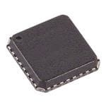
| 供应商器件封装 | 32-LFCSP-VQ(5x5) |
| 信噪比 | 71.4 dB |
| 其它名称 | AD9629BCPZ40 |
| 分辨率 | 12 bit |
| 包装 | 托盘 |
| 商标 | Analog Devices |
| 安装类型 | 表面贴装 |
| 安装风格 | SMD/SMT |
| 封装 | Tray |
| 封装/外壳 | 32-VFQFN 裸露焊盘,CSP |
| 封装/箱体 | LFCSP-32 |
| 工作温度 | -40°C ~ 85°C |
| 工作电源电压 | 1.8 V |
| 工厂包装数量 | 490 |
| 接口类型 | Parallel, Serial (SPI) |
| 数据接口 | SPI |
| 最大功率耗散 | 114 mW |
| 最大工作温度 | + 85 C |
| 最小工作温度 | - 40 C |
| 标准包装 | 1 |
| 特性 | - |
| 电压参考 | Internal, External |
| 电压源 | 模拟和数字 |
| 系列 | AD9629 |
| 结构 | Pipeline |
| 转换器数 | 1 |
| 转换器数量 | 1 |
| 转换速率 | 80 MS/s |
| 输入数和类型 | 2 个单端,单极1 个差分,单极 |
| 输入类型 | Differential |
| 通道数量 | 1 Channel |
| 采样率(每秒) | 40M |


- 商务部:美国ITC正式对集成电路等产品启动337调查
- 曝三星4nm工艺存在良率问题 高通将骁龙8 Gen1或转产台积电
- 太阳诱电将投资9.5亿元在常州建新厂生产MLCC 预计2023年完工
- 英特尔发布欧洲新工厂建设计划 深化IDM 2.0 战略
- 台积电先进制程称霸业界 有大客户加持明年业绩稳了
- 达到5530亿美元!SIA预计今年全球半导体销售额将创下新高
- 英特尔拟将自动驾驶子公司Mobileye上市 估值或超500亿美元
- 三星加码芯片和SET,合并消费电子和移动部门,撤换高东真等 CEO
- 三星电子宣布重大人事变动 还合并消费电子和移动部门
- 海关总署:前11个月进口集成电路产品价值2.52万亿元 增长14.8%


PDF Datasheet 数据手册内容提取
12-Bit, 20 MSPS/40 MSPS/65 MSPS/80 MSPS, 1.8 V Analog-to-Digital Converter Data Sheet AD9629 FEATURES FUNCTIONAL BLOCK DIAGRAM 1.8 V analog supply operation AVDD GND SDIO SCLK CSB DRVDD 1.8 V to 3.3 V output supply SNR RBIAS SPI 71.3 dBFS at 9.7 MHz input VCM 69.0 dBFS at 200 MHz input PROGRAMMING DATA FER OR SFDR VIN+ ADC OSBUF D11 (MSB) 95 dBc at 9.7 MHz input VIN– CORE CMPUT D0 (LSB) T 83 dBc at 200 MHz input U O DCO Low power VREF 45 mW at 20 MSPS SENSE 85 mW at 80 MSPS REF AD9629 SELECT Differential input with 700 MHz bandwidth On-chip voltage reference and sample-and-hold circuit DIVIDE BY MODE 1, 2, 4 CONTROLS 2 V p-p differential analog input DSeNrLia =l p±o0r.t1 6co LnStBro l options CLK+CLK– PDWN DFS MODE 08540-001 Figure 1. Offset binary, gray code, or twos complement data format Integer 1, 2, or 4 input clock divider PRODUCT HIGHLIGHTS Built-in selectable digital test pattern generation 1. The AD9629 operates from a single 1.8 V analog power Energy-saving power-down modes supply and features a separate digital output driver supply Data clock out with programmable clock and data alignment to accommodate 1.8 V to 3.3 V logic families. APPLICATIONS 2. The sample-and-hold circuit maintains excellent performance for input frequencies up to 200 MHz and is Communications designed for low cost, low power, and ease of use. Diversity radio systems 3. A standard serial port interface (SPI) supports various Multimode digital receivers product features and functions, such as data output format- GSM, EDGE, W-CDMA, LTE, CDMA2000, WiMAX, TD-SCDMA ting, internal clock divider, power-down, DCO and data Smart antenna systems output (D11 to D0) timing and offset adjustments, and Battery-powered instruments voltage reference modes. Hand held scope meters 4. The AD9629 is packaged in a 32-lead RoHS compliant Portable medical imaging LFCSP that is pin compatible with the AD9609 10-bit ADC Ultrasound and the AD9649 14-bit ADC, enabling a simple migration Radar/LIDAR path between 10-bit and 14-bit converters sampling from PET/SPECT imaging 20 MSPS to 80 MSPS. Rev. B Document Feedback Information furnished by Analog Devices is believed to be accurate and reliable. However, no responsibility is assumed by Analog Devices for its use, nor for any infringements of patents or other One Technology Way, P.O. Box 9106, Norwood, MA 02062-9106, U.S.A. rights of third parties that may result from its use. Specifications subject to change without notice. No license is granted by implication or otherwise under any patent or patent rights of Analog Devices. Tel: 781.329.4700 ©2009–2017 Analog Devices, Inc. All rights reserved. Trademarks and registered trademarks are the property of their respective owners. Technical Support www.analog.com
AD9629 Data Sheet TABLE OF CONTENTS Features .....................................................................................1 Voltage Reference ................................................................ 19 Applications...............................................................................1 Clock Input Considerations ................................................. 20 Functional Block Diagram.........................................................1 Power Dissipation and Standby Mode ................................. 21 Product Highlights ....................................................................1 Digital Outputs .................................................................... 22 Revision History ........................................................................2 Timing ................................................................................. 22 General Description ..................................................................3 Built-In Self-Test (BIST) and Output Test ............................... 23 Specifications .............................................................................4 Built-In Self-Test (BIST) ...................................................... 23 DC Specifications...................................................................4 Output Test Modes .............................................................. 23 AC Specifications ...................................................................5 Serial Port Interface (SPI)........................................................ 24 Digital Specifications .............................................................6 Configuration Using the SPI................................................ 24 Switching Specifications.........................................................7 Hardware Interface .............................................................. 25 Timing Specifications.............................................................8 Configuration Without the SPI............................................ 25 Absolute Maximum Ratings ......................................................9 SPI Accessible Features ........................................................ 25 Thermal Characteristics.........................................................9 Memory Map........................................................................... 26 ESD Caution ..........................................................................9 Reading the Memory Map Register Table ............................ 26 Pin Configuration and Function Descriptions.........................10 Open Locations ................................................................... 26 Typical Performance Characteristics .......................................11 Default Values...................................................................... 26 AD9629-80...........................................................................11 Memory Map Register Table................................................ 27 AD9629-65...........................................................................13 Memory Map Register Descriptions .................................... 29 AD9629-40...........................................................................14 Applications Information ........................................................ 30 AD9629-20...........................................................................15 Design Guidelines................................................................ 30 Equivalent Circuits ..................................................................16 Outline Dimensions ................................................................ 31 Theory of Operation................................................................17 Ordering Guide ................................................................... 31 Analog Input Considerations ...............................................17 REVISION HISTORY 2/2017—Rev. A to Rev B Added Endnote 1, Table 16 ......................................................28 Changes to Power and Ground Recommendations Section.....30 Added Soft Reset Section.........................................................30 6/2015—Rev. 0 to Rev. A Change to Product Highlights Section.......................................1 Changes to Figure 3 and Table 8 ..............................................10 Updated Outline Dimensions ..................................................31 Changes to Ordering Guide .....................................................31 10/2009—Revision 0: Initial Version Rev. B | Page 2 of 32
Data Sheet AD9629 GENERAL DESCRIPTION The AD9629 is a monolithic, single channel 1.8 V supply, 12-bit, deterministic and pseudorandom patterns, along with custom 20 MSPS/40 MSPS/65 MSPS/80 MSPS analog-to-digital conver- user-defined test patterns entered via the serial port interface (SPI). ter (ADC). It features a high performance sample-and-hold A differential clock input with optional 1, 2, or 4 divide ratios circuit and on-chip voltage reference. controls all internal conversion cycles. The product uses multistage differential pipeline architecture The digital output data is presented in offset binary, gray code, with output error correction logic to provide 12-bit accuracy at or twos complement format. A data output clock (DCO) is 80 MSPS data rates and to guarantee no missing codes over the provided to ensure proper latch timing with receiving logic. Both full operating temperature range. 1.8 V and 3.3 V CMOS levels are supported. The ADC contains several features designed to maximize The AD9629 is available in a 32-lead RoHS compliant LFCSP flexibility and minimize system cost, such as programmable and is specified over the industrial temperature range (−40°C clock and data alignment and programmable digital test pattern to +85°C). generation. The available digital test patterns include built-in Rev. B | Page 3 of 32
AD9629 Data Sheet SPECIFICATIONS DC SPECIFICATIONS AVDD = 1.8 V; DRVDD = 1.8 V, maximum sample rate, 2 V p-p differential input, 1.0 V internal reference; AIN = −1.0 dBFS, 50% duty cycle clock, unless otherwise noted. Table 1. AD9629-20/AD9629-40 AD9629-65 AD9629-80 Parameter Temp Min Typ Max Min Typ Max Min Typ Max Unit RESOLUTION Full 12 12 12 Bits ACCURACY No Missing Codes Full Guaranteed Guaranteed Guaranteed Offset Error Full −0.40 +0.05 +0.50 −0.40 +0.05 +0.50 −0.40 +0.05 +0.50 % FSR Gain Error1 Full −1.5 −1.5 −1.5 % FSR Differential Nonlinearity (DNL)2 Full ±0.25 ±0.25 ±0.30 LSB 25°C ±0.11 ±0.11 ±0.16 LSB Integral Nonlinearity (INL)2 Full ±0.40 ±0.30 ±0.35 LSB 25°C ±0.11 ±0.13 ±0.16 LSB TEMPERATURE DRIFT Offset Error Full ±2 ±2 ±2 ppm/°C INTERNAL VOLTAGE REFERENCE Output Voltage (1 V Mode) Full 0.984 0.996 1.008 0.984 0.996 1.008 0.984 0.996 1.008 V Load Regulation Error at 1.0 mA Full 2 2 2 mV INPUT-REFERRED NOISE VREF = 1.0 V 25°C 0.25 0.25 0.25 LSB rms ANALOG INPUT Input Span, VREF = 1.0 V Full 2 2 2 V p-p Input Capacitance3 Full 6 6 6 pF Input Common-Mode Voltage Full 0.9 0.9 0.9 V Input Common-Mode Range Full 0.5 1.3 0.5 1.3 0.5 1.3 V REFERENCE INPUT RESISTANCE Full 7.5 7.5 7.5 kΩ POWER SUPPLIES Supply Voltage AVDD Full 1.7 1.8 1.9 1.7 1.8 1.9 1.7 1.8 1.9 V DRVDD Full 1.7 3.6 1.7 3.6 1.7 3.6 V Supply Current IAVDD2 Full 24.9/31.1 26.7/33.2 41.2 46.0 46.8 50.0 mA IDRVDD2 (1.8 V) Full 1.5/2.5 4.2 5.0 mA IDRVDD2 (3.3 V) Full 2.7/4.7 7.5 9.0 mA POWER CONSUMPTION DC Input Full 45.0/56.7 75 85.2 mW Sine Wave Input2 (DRVDD = 1.8 V) Full 47.5/60.5 50.7/65.0 81.7 86.0 93 100 mW Sine Wave Input2 (DRVDD = 3.3 V) Full 53.7/71.7 98.9 114 mW Standby Power4 Full 34 34 34 mW Power-Down Power Full 0.5 0.5 0.5 mW 1 Measured with 1.0 V external reference. 2 Measured with a 10 MHz input frequency at rated sample rate, full-scale sine wave, with approximately 5 pF loading on each output bit. 3 Input capacitance refers to the effective capacitance between one differential input pin and AGND. 4 Standby power is measured with a dc input and the clock active. Rev. B | Page 4 of 32
Data Sheet AD9629 AC SPECIFICATIONS AVDD = 1.8 V; DRVDD = 1.8 V, maximum sample rate, 2 V p-p differential input, 1.0 V internal reference; AIN = −1.0 dBFS, 50% duty cycle clock, unless otherwise noted. Table 2. AD9629-20/AD9629-40 AD9629-65 AD9629-80 Parameter1 Temp Min Typ Max Min Typ Max Min Typ Max Unit SIGNAL-TO-NOISE RATIO (SNR) f = 9.7 MHz 25°C 71.4 71.3 71.3 dBFS IN f = 30.5 MHz 25°C 71.2 71.2 71.2 dBFS IN Full 70.5/70.7 70.6 dBFS f = 70 MHz 25°C 70.5/71.0 71.0 70.9 dBFS IN Full 70.3 dBFS f = 200 MHz 25°C 69.0 69.0 dBFS IN SIGNAL-TO-NOISE-AND-DISTORTION (SINAD) f = 9.7 MHz 25°C 71.4 71.3 71.2 dBFS IN f = 30.5 MHz 25°C 71.2 71.2 71.1 dBFS IN Full 70.5/70.6 70.5 dBFS f = 70 MHz 25°C 70.4/70.9 70.9 70.8 dBFS IN Full 70.2 dBFS f = 200 MHz 25°C 68 68 68 dBFS IN EFFECTIVE NUMBER OF BITS (ENOB) f = 9.7 MHz 25°C 11.4/11.6 11.6 11.5 Bits IN f = 30.5 MHz 25°C 11.4/11.5 11.5 11.5 Bits IN f = 70 MHz 25°C 11.4/11.5 11.5 11.5 Bits IN f = 200 MHz 25°C 11.0 11.0 11.0 Bits IN WORST SECOND OR THIRD HARMONIC f = 9.7 MHz 25°C −97 −97 −95 dBc IN f = 30.5 MHz 25°C −95 −95 −94 dBc IN Full −83 −83 dBc f = 70 MHz 25°C −96/−94 −95 −95 dBc IN Full −81 dBc f = 200 MHz 25°C −83 −83 −83 dBc IN SPURIOUS-FREE DYNAMIC RANGE (SFDR) f = 9.7 MHz 25°C 97 97 95 dBc IN f = 30.5 MHz 25°C 96/95 95 93 dBc IN Full 83 83 dBc f = 70 MHz 25°C 96/94 95 95 dBc IN Full 81 dBc f = 200 MHz 25°C 83 83 83 dBc IN WORST OTHER (HARMONIC OR SPUR) f = 9.7 MHz 25°C −100 −100 −100 dBc IN f = 30.5 MHz 25°C −100 −100 −100 dBc IN Full −92/−91 −93 dBc f = 70 MHz 25°C −97/−100 −100 −100 dBc IN Full −89 dBc f = 200 MHz 25°C −92 −92 −92 dBc IN TWO-TONE SFDR f = 30.5 MHz (−7 dBFS), 32.5 MHz (−7 dBFS) 25°C 90 90 90 dBc IN ANALOG INPUT BANDWIDTH 25°C 700 700 700 MHz 1 See the AN-835 Application Note, Understanding High Speed ADC Testing and Evaluation, for a complete set of definitions. Rev. B | Page 5 of 32
AD9629 Data Sheet DIGITAL SPECIFICATIONS AVDD = 1.8 V; DRVDD = 1.8 V, maximum sample rate, 2 V p-p differential input, 1.0 V internal reference; AIN = −1.0 dBFS, 50% duty cycle clock, unless otherwise noted. Table 3. AD9629-20/AD9629-40/AD9629-65/AD9629-80 Parameter Temp Min Typ Max Unit DIFFERENTIAL CLOCK INPUTS (CLK+, CLK−) Logic Compliance CMOS/LVDS/LVPECL Internal Common-Mode Bias Full 0.9 V Differential Input Voltage Full 0.2 3.6 V p-p Input Voltage Range Full GND − 0.3 AVDD + 0.2 V High Level Input Current Full −10 +10 µA Low Level Input Current Full −10 +10 µA Input Resistance Full 8 10 12 kΩ Input Capacitance Full 4 pF LOGIC INPUTS (SCLK/DFS, MODE, SDIO/PDWN)1 High Level Input Voltage Full 1.2 DRVDD + 0.3 V Low Level Input Voltage Full 0 0.8 V High Level Input Current Full −50 −75 µA Low Level Input Current Full −10 +10 µA Input Resistance Full 30 kΩ Input Capacitance Full 2 pF LOGIC INPUTS (CSB)2 High Level Input Voltage Full 1.2 DRVDD + 0.3 V Low Level Input Voltage Full 0 0.8 V High Level Input Current Full −10 +10 µA Low Level Input Current Full 40 135 µA Input Resistance Full 26 kΩ Input Capacitance Full 2 pF DIGITAL OUTPUTS DRVDD = 3.3 V High Level Output Voltage, I = 50 µA Full 3.29 V OH High Level Output Voltage, I = 0.5 mA Full 3.25 V OH Low Level Output Voltage, I = 1.6 mA Full 0.2 V OL Low Level Output Voltage, I = 50 µA Full 0.05 V OL DRVDD = 1.8 V High Level Output Voltage, I = 50 µA Full 1.79 V OH High Level Output Voltage, I = 0.5 mA Full 1.75 V OH Low Level Output Voltage, I = 1.6 mA Full 0.2 V OL Low Level Output Voltage, I = 50 µA Full 0.05 V OL 1 Internal 30 kΩ pull-down. 2 Internal 30 kΩ pull-up. Rev. B | Page 6 of 32
Data Sheet AD9629 SWITCHING SPECIFICATIONS AVDD = 1.8 V; DRVDD = 1.8 V, maximum sample rate, 2 V p-p differential input, 1.0 V internal reference; AIN = −1.0 dBFS, 50% duty cycle clock, unless otherwise noted. Table 4. AD9629-20/AD9629-40 AD9629-65 AD9629-80 Parameter Temp Min Typ Max Min Typ Max Min Typ Max Unit CLOCK INPUT PARAMETERS Input Clock Rate1 Full 80/160 260 320 MHz Conversion Rate2 Full 3 20/40 3 65 3 80 MSPS CLK Period, Divide-by-1 Mode (t ) Full 50/25 15.38 12.5 ns CLK CLK Pulse Width High (t ) 25.0/12.5 7.69 6.25 ns CH Aperture Delay (t ) Full 1.0 1.0 1.0 ns A Aperture Uncertainty (Jitter, t) Full 0.1 0.1 0.1 ps rms J DATA OUTPUT PARAMETERS Data Propagation Delay (tPD) Full 3 3 3 ns DCO Propagation Delay (tDCO) Full 3 3 3 ns DCO to Data Skew (tSKEW) Full 0.1 0.1 0.1 ns Pipeline Delay (Latency) Full 8 8 8 Cycles Wake-Up Time3 Full 350 350 350 μs Standby Full 600/400 300 260 ns OUT-OF-RANGE RECOVERY TIME Full 2 2 2 Cycles 1 Input clock rate is the clock rate before the internal CLK divider. 2 Conversion rate is the clock rate after the CLK divider. 3 Wake-up time is dependent on the value of the decoupling capacitors. N – 1 t N + 4 A N + 5 N N + 3 VIN N + 1 N + 2 t CH t CLK CLK+ CLK– t DCO DCO t SKEW DATA N – 8 N – 7 N – 6 N – 5 N – 4 tPD 08540-002 Figure 2. CMOS Output Data Timing Rev. B | Page 7 of 32
AD9629 Data Sheet TIMING SPECIFICATIONS Table 5. Parameter Conditions Min Typ Max Unit SPI TIMING REQUIREMENTS t Setup time between the data and the rising edge of SCLK 2 ns DS t Hold time between the data and the rising edge of SCLK 2 ns DH t Period of the SCLK 40 ns CLK t Setup time between CSB and SCLK 2 ns S t Hold time between CSB and SCLK 2 ns H t SCLK pulse width high 10 ns HIGH t SCLK pulse width low 10 ns LOW t Time required for the SDIO pin to switch from an input to an 10 ns EN_SDIO output relative to the SCLK falling edge t Time required for the SDIO pin to switch from an output to an 10 ns DIS_SDIO input relative to the SCLK rising edge Rev. B | Page 8 of 32
Data Sheet AD9629 ABSOLUTE MAXIMUM RATINGS THERMAL CHARACTERISTICS Table 6. Parameter Rating The exposed paddle is the only ground connection for the chip. AVDD to AGND −0.3 V to +2.0 V The exposed paddle must be soldered to the AGND plane of the DRVDD to AGND −0.3 V to +3.9 V user’s circuit board. Soldering the exposed paddle to the user’s VIN+, VIN− to AGND −0.3 V to AVDD + 0.2 V board also increases the reliability of the solder joints and CLK+, CLK− to AGND −0.3 V to AVDD + 0.2 V maximizes the thermal capability of the package. VREF to AGND −0.3 V to AVDD + 0.2 V SENSE to AGND −0.3 V to AVDD + 0.2 V Table 7. Thermal Resistance VCM to AGND −0.3 V to AVDD + 0.2 V Airflow Package Velocity RBIAS to AGND −0.3 V to AVDD + 0.2 V Type (m/sec) θ 1, 2 θ 1, 3 θ 1, 4 Ψ 1, 2 Unit CSB to AGND −0.3 V to DRVDD + 0.3 V JA JC JB JT 32-Lead 0 37.1 3.1 20.7 0.3 °C/W SCLK/DFS to AGND −0.3 V to DRVDD + 0.3 V LFCSP 1.0 32.4 0.5 °C/W SDIO/PDWN to AGND −0.3 V to DRVDD + 0.3 V 5 mm × MODE/OR to AGND −0.3 V to DRVDD + 0.3 V 2.5 29.1 0.8 °C/W 5 mm D0 through D11 to AGND −0.3 V to DRVDD + 0.3 V DCO to AGND −0.3 V to DRVDD + 0.3 V 1 Per JEDEC 51-7, plus JEDEC 51-5 2S2P test board. Operating Temperature Range (Ambient) −40°C to +85°C 2 Per JEDEC JESD51-2 (still air) or JEDEC JESD51-6 (moving air). 3 Per MIL-Std 883, Method 1012.1. Maximum Junction Temperature Under Bias 150°C 4 Per JEDEC JESD51-8 (still air). Storage Temperature Range (Ambient) −65°C to +150°C Typical θ is specified for a 4-layer PCB with a solid ground JA plane. As shown in Table 7, airflow improves heat dissipation, Stresses at or above those listed under Absolute Maximum which reduces θ . In addition, metal in direct contact with the JA Ratings may cause permanent damage to the product. This is a package leads from metal traces, through holes, ground, and stress rating only; functional operation of the product at these power planes, reduces the θ . JA or any other conditions above those indicated in the operational section of this specification is not implied. Operation beyond the maximum operating conditions for extended periods may ESD CAUTION affect product reliability. Rev. B | Page 9 of 32
AD9629 Data Sheet PIN CONFIGURATION AND FUNCTION DESCRIPTIONS DDVA+NIV–NIVDDVASABIRMCVESNESFERV 21098765 33322222 CLK+ 1 24 AVDD CLK– 2 23 MODE/OR AVDD 3 AD9629 22 DCO CSB 4 21 D11 (MSB) SCLK/DFS 5 TOP VIEW 20 D10 (Not to Scale) SDIO/PDWN 6 19 D9 NIC 7 18 D8 NIC 8 17 D7 910111213141516 0123D456 DDDDDDDD )BSL VRD ( NOTES 1. NIC = NOT INTERNALLY CONNECTED. 2. THE EXPOSEDPADDLE IS THE ONLY GROUND CONNECTION. IT MUST BE SOLDEREDTO THEANALOG GROUND OF THE ACSNTURDSE TMONAGMXTEIHMR ’IBZSEE PN HCEEBFAITTTOS D .EISNSSIUPARTEI OPNR,O NPOEIRS EF,UANNCDT IMOENCAHLAITNYICAL 08540-003 Figure 3. Pin Configuration Table 8. Pin Function Description Pin No. Mnemonic Description 0 (EPAD) GND Exposed Paddle. The exposed paddle is the only ground connection. It must be soldered to the analog ground of the customer’s PCB to ensure proper functionality and maximize heat dissipation, noise, and mechanical strength benefits. 1, 2 CLK+, CLK− Differential Encode Clock. PECL, LVDS, or 1.8 V CMOS inputs. 3, 24, 29, 32 AVDD 1.8 V Supply Pin for ADC Core Domain. 4 CSB SPI Chip Select. Active low enable. 30 kΩ internal pull-up. 5 SCLK/DFS SPI Clock Input in SPI Mode (SCLK). 30 kΩ internal pull-down. Data Format Select in Non-SPI Mode (DFS). Static control of data output format. 30 kΩ internal pull-down. DFS high = twos complement output; DFS low = offset binary output. 6 SDIO/PDWN SPI Data Input/Output (SDIO). Bidirectional SPI data I/O in SPI mode. 30 kΩ internal pull-down. Non-SPI Mode Power-Down (PDWN). Static control of power-down with 30 kΩ internal pull-down. See Table 14 for details. 7, 8 NIC Not Internally Connected. 9 to 12, 14 to 21 D0 (LSB) to ADC Digital Outputs. D11 (MSB) 13 DRVDD 1.8 V to 3.3 V Supply Pin for Output Driver Domain. 22 DCO Data Clock Digital Output. 23 MODE/OR Chip Mode Select Input or Out-of-Range (OR) Digital Output in SPI Mode. Default = out-of-range (OR) digital output (SPI Register 0x2A[0] = 1). Option = chip mode select input (SPI Register 0x2A[0] = 0). Chip power down (SPI Register 0x08[7:5] = 100b). Chip standby (SPI Register 0x08[7:5] = 101b). Normal operation, output disabled (SPI Register 0x08[7:5] = 110b). Normal operation, output enabled (SPI Register 0x08[7:5] = 111b). Out-of-Range (OR) digital output only in non-SPI mode. 25 VREF 1.0 V Voltage Reference Input/Output. See Table 10. 26 SENSE Reference Mode Selection. See Table 10. 27 VCM Analog Output Voltage at Mid AVDD Supply. Sets common mode of the analog inputs. 28 RBIAS Sets Analog Current Bias. Connect to 10 kΩ (1% tolerance) resistor to ground. 30, 31 VIN−, VIN+ ADC Analog Inputs. Rev. B | Page 10 of 32
Data Sheet AD9629 TYPICAL PERFORMANCE CHARACTERISTICS AD9629-80 AVDD = 1.8 V; DRVDD = 1.8 V, maximum sample rate, 2 V p-p differential input, 1.0 V internal reference; AIN = −1.0 dBFS, 50% duty cycle clock, unless otherwise noted. 0 0 80MSPS –15 9.7MHz @ –1dBFS –15 80MSPS 30.6MHz @ –1dBFS SNR = 70.2dB (71.2dBFS) –30 SFDR = 93.6dBc –30 SNR = 70.1dB (71.1dBFS) SFDR = 94.4dBc S) –45 S) –45 BF BF E (d –60 E (d –60 D D PLITU –75 PLITU –75 AM –90 2 + AM –90 + 6 3 5 4 5 3 2 6 4 –105 –105 –120 –120 –135 –135 0 4 8 12 FR1E6QUE2N0CY (M24Hz) 28 32 36 40 08540-054 0 4 8 12 FR1E6QUE2N0CY (M24Hz) 28 32 36 40 08540-055 Figure 4. AD9629-80 Single-Tone FFT with fIN = 9.7 MHz Figure 7. AD9629-80 Single-Tone FFT with fIN = 30.6 MHz 0 0 80MSPS 80MSPS –15 69MHz @ –1dBFS –15 210.3MHz @ –1dBFS SNR = 69.9dB (70.9dBFS) SNR = 67.9dB (68.9dBFS) –30 SFDR = 94.3dBc –30 SFDR = 83.2dBc S) –45 S) –45 F F B B E (d –60 E (d –60 D D TU –75 TU –75 PLI PLI 3 2 AM –90 + 6 2 5 3 4 AM –90 5 6 + 4 –105 –105 –120 –120 –135 –135 0 4 8 12 FR1E6QUE2N0CY (M24Hz) 28 32 36 40 08540-056 0 4 8 12 FR1E6QUE2N0CY (M24Hz) 28 32 36 40 08540-058 Figure 5. AD9629-80 Single-Tone FFT with fIN = 69 MHz Figure 8. AD9629-80 Single-Tone FFT with fIN = 210.3 MHz 0 0 80MSPS –15 28.3 @ –7dBFS –20 30.6 @ –7dBFS –30 SFDR = 90dBc S) SFDR (dBc) F S) –45 dB –40 BF Bc/ DE (d –60 D3 (d –60 IMD3 (dBc) LITU –75 R/IM P D AM –90 F2 – F1 2F2 – F1 F1 + F22F2 – F1 2F1 – F2 SF –80 2F1 + F2 –105 SFDR (dBFS) –100 –120 IMD3 (dBFS) –135 –120 0 4 8 12 FR1E6QUE2N0CY (M24Hz) 28 32 36 40 08540-059 –70 –60 –I5N0PUT AM–4P0LITUDE– (3d0BFS) –20 –10 08540-060 Figure 6. AD9629-80 Two-Tone FFT with fIN1 = 28.3 MHz and fIN2 = 30.6 MHz Figure 9. Two-Tone SFDR/IMD3 vs. Input Amplitude (AIN) with fIN1 = 30.5 MHz and fIN2 = 32.5 MHz Rev. B | Page 11 of 32
AD9629 Data Sheet AVDD = 1.8 V; DRVDD = 1.8 V, maximum sample rate, 2 V p-p differential input, 1.0 V internal reference; AIN = −1.0 dBFS, 50% duty cycle clock, unless otherwise noted. 100 0.3 SFDR 90 0.2 80 SNR dBc) 70 B) 0.1 R (dBFS/ 5600 ROR (LS 0 D R SF 40 L E NR/ DN–0.1 S 30 20 –0.2 10 00 50 INPUT FREQ10U0ENCY (MHz)150 200 08540-061 –0.30 500 1000 150O0UTP20U0T0 CO2D5E00 3000 3500 4000 08540-063 Figure 10. AD9629-80 SNR/SFDR vs. Input Frequency (AIN) with 2 V p-p Full Scale Figure 13. DNL Error with fIN = 9.7 MHz 100 0.4 90 SFDR 80 c) SNRFS 0.2 B 70 R (dBFS/d 5600 OR (LSB) 0 D R F R S/S 40 L E F N R I N 30 S –0.2 20 10 010 20 30 SAM40PLE RA5T0E (MHz)60 70 80 08540-062 0.40 500 1000 150O0UTP20U0T0 CO2D5E00 3000 3500 4000 08540-066 Figure 11. AD9629-80 SNR/SFDR vs. Sample Rate with AIN = 9.7 MHz Figure 14. INL with f = 9.7 MHz IN 100 90 SFDRFS 80 S) SNRFS F B 70 d D N 60 A SFDR c B 50 d R ( SNR D 40 F S R/ 30 N S 20 10 0 –70 –60 –50INPUT– 4A0MPLIT–U3D0E (dBc–)20 –10 0 08540-064 Figure 12. AD9629-80 SNR/SFDR vs. Input Amplitude (AIN) with f = 9.7 MHz IN Rev. B | Page 12 of 32
Data Sheet AD9629 AD9629-65 AVDD = 1.8 V; DRVDD = 1.8 V, maximum sample rate, 2 V p-p differential input, 1.0 V internal reference; AIN = −1.0 dBFS, 50% duty cycle clock, unless otherwise noted. 0 120 65MSPS –15 9.7MHz @ –1dBFS SFDRFS SNR =70.3 (71.3dBFS) 100 –30 SFDR = 94.2dBc S) F S) –45 dB 80 DE (dBF –60 Bc AND 60 SNRFS PLITU –75 DR (d SFDR AM –90 6 + 5 2 4 3 NR/SF 40 –105 S SNR 20 –120 –135 0 0 3 6 9 F12REQ1U5ENC1Y8 (MH2z1) 24 27 30 33 08540-067 –70 –60 –50INPUT– 4A0MPLIT–U3D0E (dBc–)20 –10 0 08540-070 Figure 15. AD9629-65 Single-Tone FFT with fIN = 9.7 MHz Figure 18. AD9629-65 SNR/SFDR vs. Input Amplitude (AIN) with fIN = 9.7 MHz 0 100 65MSPS –15 69MHz @ –1dBFS 90 SFDR SNR = 69.9dB (70.9dBFS) –30 SFDR = 92.0dBc 80 SNR S) –45 Bc) 70 F d PLITUDE (dB ––6705 SFDR (dBFS/ 456000 AM –90 2 3 4 +5 6 SNR/ 30 –105 20 –120 10 –1350 3 6 9 F12REQ1U5ENC1Y8 (MH2z1) 24 27 30 33 08540-068 00 50 INPUT F1R00EQUENCY (M1H50z) 200 08540-071 Figure 16. AD9629-65 Single-Tone FFT with fIN = 69 MHz Figure 19. AD9629-65 SNR/SFDR vs. Input Frequency (AIN) with 2 V p-p Full Scale 0 –15 65MSPS 30.6MHz @ –1dBFS –30 SNR = 70.2dB (71.2dBFS) SFDR = 94.1dBc S) –45 F B E (d –60 D U T –75 LI P AM –90 2 + 5 3 4 6 –105 –120 –135 0 3 6 9 F12REQ1U5ENC1Y8 (MH2z1) 24 27 30 33 08540-069 Figure 17. AD9629-65 Single-Tone FFT with fIN = 30.6 MHz Rev. B | Page 13 of 32
AD9629 Data Sheet AD9629-40 AVDD = 1.8 V; DRVDD = 1.8 V, maximum sample rate, 2 V p-p differential input, 1.0 V internal reference; AIN = −1.0 dBFS, 50% duty cycle clock, unless otherwise noted. 0 120 40MSPS –15 9.7MHz @ –1dBFS SFDRFS SNR = 70.3dB (71.3dBFS) 100 –30 SFDR = 93.8dBc S) F S) –45 dB 80 E (dBF –60 c AND SNRFS D B 60 U d AMPLIT–1––079550 4 5 3 + 6 2 SNR/SFDR ( 40 SSFNDRR 20 –120 –135 0 0 2 4 6 FRE8QUE1N0CY (M12Hz) 14 16 18 20 08540-072 –70 –60 –50INPUT– A40MPLIT–U3D0E (dBc–)20 –10 0 08540-074 Figure 20. AD9629-40 Single-Tone FFT with fIN = 9.7 MHz Figure 22. AD9629-40 SNR/SFDR vs. Input Amplitude (AIN) with fIN = 9.7 MHz 0 –15 40MSPS 30.6MHz @ –1dBFS –30 SNR = 70.2dB (71.2dBFS) SFDR = 95.4dBc S) –45 F B E (d –60 D U T –75 LI P AM –90 + –105 4 5 3 6 2 –120 –135 0 2 4 6 FRE8QUE1N0CY (M12Hz) 14 16 18 20 08540-073 Figure 21. AD9629-40 Single-Tone FFT with fIN = 30.6 MHz Rev. B | Page 14 of 32
Data Sheet AD9629 AD9629-20 AVDD = 1.8 V; DRVDD = 1.8 V, maximum sample rate, 2 V p-p differential input, 1.0 V internal reference; AIN = −1.0 dBFS, 50% duty cycle clock, unless otherwise noted. 0 120 –15 20MSPS 9.7MHz @ –1dBFS 100 SFDRFS –30 SNR = 70.3dB (71.3dBFS) SFDR = 94.1dBc S) F S) –45 dB 80 DE (dBF –60 Bc AND 60 SNRFS AMPLITU ––7950 2 4 + 5 3 NR/SFDR (d 40 SSFNDRR –105 6 S 20 –120 –1350 0.95 1.90 2.85 3F.R8E0QU4.E7N5CY5. 7(M0Hz6).65 7.60 8.55 9.50 08540-075 0–70 –60 –50INPUT– 4A0MPLITU–3D0E (dBc–)20 –10 0 08540-077 Figure 23. AD9629-20 Single-Tone FFT with fIN = 9.7 MHz Figure 25. AD9629-20 SNR/SFDR vs. Input Amplitude (AIN) with fIN = 9.7 MHz 0 –15 20MSPS 30.6MHz @ –1dBFS SNR = 70.2dB (71.2dBFS) –30 SFDR = 94.6dBc S) –45 F B d E ( –60 D U T –75 LI P AM –90 + 2 4 6 5 3 –105 –120 –1350 0.95 1.90 2.85 3F.R8E0QU4.E7N5CY5. 7(M0Hz6).65 7.60 8.55 9.50 08540-076 Figure 24. AD9629-20 Single-Tone FFT with fIN = 30.6 MHz Rev. B | Page 15 of 32
AD9629 Data Sheet EQUIVALENT CIRCUITS DRVDD AVDD VIN± 08540-039 08540-042 Figure 26. Equivalent Analog Input Circuit Figure 30. Equivalent D0 to D11 and OR Digital Output Circuit AVDD DRVDD SCLK/DFS, MODE, 350Ω VREF 375Ω SDIO/PDWN 30kΩ 7.5kΩ 08540-047 08540-043 Figure 27. Equivalent VREF Circuit Figure 31. Equivalent SCLK/DFS, MODE, and SDIO/PDWN Input Circuit AVDD DRVDD AVDD 30kΩ 375Ω 350Ω SENSE CSB 08540-046 08540-045 Figure 28. Equivalent SENSE Circuit Figure 32. Equivalent CSB Input Circuit 5Ω CLK+ 15kΩ 0.9V AVDD 15kΩ 5Ω CLK– RBIAS 375Ω AND VCM 08540-040 08540-044 Figure 29. Equivalent Clock Input Circuit Figure 33. Equivalent RBIAS and VCM Circuit Rev. B | Page 16 of 32
Data Sheet AD9629 THEORY OF OPERATION high IF frequencies. Either a shunt capacitor or two single-ended The AD9629 architecture consists of a multistage, pipelined ADC. capacitors can be placed on the inputs to provide a matching Each stage provides sufficient overlap to correct for flash errors in passive network. This ultimately creates a low-pass filter at the the preceding stage. The quantized outputs from each stage are input to limit unwanted broadband noise. See the AN-742 combined into a final 12-bit result in the digital correction logic. Application Note, the AN-827 Application Note, and the Analog The pipelined architecture permits the first stage to operate with a Dialogue article “Transformer-Coupled Front-End for Wideband new input sample while the remaining stages operate with pre- A/D Converters” (Volume 39, April 2005) for more information. ceding samples. Sampling occurs on the rising edge of the clock. In general, the precise values depend on the application. Each stage of the pipeline, excluding the last, consists of a low Input Common Mode resolution flash ADC connected to a switched-capacitor DAC and an interstage residue amplifier (for example, a multiplying The analog inputs of the AD9629 are not internally dc-biased. digital-to-analog converter (MDAC)). The residue amplifier Therefore, in ac-coupled applications, the user must provide a magnifies the difference between the reconstructed DAC output dc bias externally. Setting the device so that VCM = AVDD/2 and the flash input for the next stage in the pipeline. One bit of is recommended for optimum performance, but the device can redundancy is used in each stage to facilitate digital correction function over a wider range with reasonable performance, as of flash errors. The last stage consists of a flash ADC. shown in Figure 35 and Figure 36. The output staging block aligns the data, corrects errors, and An on-board, common-mode voltage reference is included in passes the data to the CMOS output buffers. The output buffers the design and is available from the VCM pin. The VCM pin are powered from a separate (DRVDD) supply, allowing adjust- must be decoupled to ground by a 0.1 μF capacitor, as described ment of the output voltage swing. During power-down, the output in the Applications Information section. buffers go into a high impedance state. 100 ANALOG INPUT CONSIDERATIONS SFDR (dBc) The analog input to the AD9629 is a differential switched- 90 capacitor circuit designed for processing differential input c) B signals. This circuit can support a wide common-mode range d S/ 80 F while maintaining excellent performance. By using an input B d common-mode voltage of midsupply, users can minimize R ( SNR (dBFS) D signal-dependent errors and achieve optimum performance. SF 70 R/ N S 60 H VIN+ CPAR CSAMPLE H 500.5 0.6 IN0P.U7T CO0M.8MON-M0.O9DE V1O.0LTAGE1. 1(V) 1.2 1.3 08540-149 Figure 35. SNR/SFDR vs. Input Common-Mode Voltage, S S S S fIN = 32.1 MHz, fS = 80 MSPS CSAMPLE 100 VIN– C H PAR SFDR (dBc) H 08540-006 Bc) 90 Figure 34. Switched-Capacitor Input Circuit d S/ 80 F B The clock signal alternately switches the input circuit between d R ( SNR (dBFS) sample-and-hold mode (see Figure 34). When the input circuit D SF 70 is switched to sample mode, the signal source must be capable R/ N of charging the sample capacitors and settling within one-half S of a clock cycle. A small resistor in series with each input can 60 help reduce the peak transient current injected from the output sbfetearageden sto icfa alt hnce ab pdear pciviltianacnge cdseo o uanrt c teeha. ecI nha naledagldo iogtif o itnnhp,e lu oitnwsp aQunt d itn,o dt hrueecdrtoeufrcose ro ehr,i fagechrh rdiietiefv- e 500.5 0.6 IN0P.U7T CO0M.8MON-M0.O9DE V1O.0LTAGE1. 1(V) 1.2 1.3 08540-150 Figure 36. SNR/SFDR vs. Input Common-Mode Voltage, the maximum bandwidth of the ADC. Such use of low Q inductors fIN = 10.3 MHz, fS = 20 MSPS or ferrite beads is required when driving the converter front end at Rev. B | Page 17 of 32
AD9629 Data Sheet Differential Input Configurations ~10 MHz where SNR is a key parameter, differential double balun coupling is the recommended input configuration (see Figure 40). Optimum performance is achieved while driving the AD9629 in a differential input configuration. For baseband applications, the An alternative to using a transformer-coupled input at frequencies AD8138, ADA4937-2, and ADA4938-2 differential drivers provide in the second Nyquist zone is to use the AD8352 differential driver. excellent performance and a flexible interface to the ADC. An example is shown in Figure 41. See the AD8352 data sheet The output common-mode voltage of the ADA4938-2 is easily for more information. set with the VCM pin of the AD9629 (see Figure 37), and the In any configuration, the value of Shunt Capacitor C is dependent driver can be configured in a Sallen-Key filter topology to on the input frequency and source impedance and may need to provide band limiting of the input signal. be reduced or removed. Table 9 displays the suggested values to set 200Ω 33Ω the RC network. However, these values are dependent on the VIN 76.8Ω VIN– AVDD 90Ω input signal and should be used only as a starting guide. ADA4938 10pF ADC Table 9. Example RC Network 0.1µF 120Ω 200Ω 33Ω VIN+ VCM 08540-007 Frequency Range (MHz) R(Ω S Eearicehs) C Differential (pF) Figure 37. Differential Input Configuration Using the ADA4938-2 0 to 70 33 22 70 to 200 125 Open For baseband applications below ~10 MHz where SNR is a key parameter, differential transformer-coupling is the recommended input configuration. An example is shown in Figure 38. To bias Single-Ended Input Configuration the analog input, the VCM voltage can be connected to the A single-ended input can provide adequate performance in center tap of the secondary winding of the transformer. cost-sensitive applications. In this configuration, SFDR and distortion performance degrade due to the large input common- VIN+ R mode swing. If the source impedances on each input are matched, 2V p-p 49.9Ω C ADC there should be little effect on SNR performance. Figure 39 R VIN– VCM shows a typical single-ended input configuration. 0.1µF 08540-008 10µF 1kAΩVDD R Figure 38. Differential Transformer-Coupled Configuration VIN+ 1Vp-p 49.9Ω 0.1µF 1kΩ The signal characteristics must be considered when selecting AVDD C ADC a transformer. Most RF transformers saturate at frequencies 1kΩ R balesloo wca ua sfee wco mree sgaathuerrattzio (nM, wHhzi)c. hE xlecaedsssi vtoe sdiigsntoarlt pioonw. er can 10µF 0.1µF 1kΩ VIN– 08540-009 At input frequencies in the second Nyquist zone and above, the Figure 39. Single-Ended Input Configuration noise performance of most amplifiers is not adequate to achieve the true SNR performance of the AD9629. For applications above 0.1µF 0.1µF R 2V p-p VIN+ 25Ω PA S S P C ADC 25Ω 0.1µF 0.1µF R VIN– VCM 08540-010 Figure 40. Differential Double Balun Input Configuration VCC 0.1µF ANALOG INPUT 0Ω 161 8, 1311 0.1µF 0.1µF R VIN+ 2 200Ω CD RD RG34 AD835210 0.1µF 200Ω R C VIN– ADCVCM ANALOG INPUT 0.1µF 0Ω 5 104.1µF 0.1µF 08540-011 Figure 41. Differential Input Configuration Using the AD8352 Rev. B | Page 18 of 32
Data Sheet AD9629 VOLTAGE REFERENCE External Reference Operation A stable and accurate 1.0 V voltage reference is built into the The use of an external reference may be necessary to enhance AD9629. The VREF can be configured using either the internal the gain accuracy of the ADC or improve thermal drift charac- 1.0 V reference or an externally applied 1.0 V reference voltage. teristics. Figure 44 shows the typical drift characteristics of the The various reference modes are summarized in the sections internal reference in 1.0 V mode. that follow. The Reference Decoupling section describes the 4 best practices PCB layout of the reference. 3 Internal Reference Connection 2 VREF ERROR (mV) A comparator within the AD9629 detects the potential at the 1 SwEhNicShE a prein s uanmdm coarnifziegdu riens Tthaeb lree f1e0re. nIfc SeE inNtoS Etw iso g proosusnibdlee dm, tohdee s, OR (mV) 0 R –1 reference amplifier switch is connected to the internal resistor R E divider (see Figure 42), setting VREF to 1.0 V. EF –2 R V –3 VIN+ –4 VIN– –5 –6 CAODRCE –40 –20 0TEMPER2A0TURE (°4C0) 60 80 08540-052 Figure 44. Typical VREF Drift VREF When the SENSE pin is tied to AVDD, the internal reference is 1.0µF 0.1µF SELECT disabled, allowing the use of an external reference. An internal LOGIC reference buffer loads the external reference with an equivalent SENSE 7.5 kΩ load (see Figure 27). The internal buffer generates the 0.5V positive and negative full-scale references for the ADC core. Therefore, the external reference must be limited to a maximum ADC 08540-012 of 1.0 V. Figure 42. Internal Reference Configuration If the internal reference of the AD9629 is used to drive multiple converters to improve gain matching, the loading of the reference by the other converters must be considered. Figure 43 shows how the internal reference voltage is affected by loading. 0 %)–0.5 R ( O R R–1.0 E GE INTERNAL VREF = 0.996V A T–1.5 L O V E C N–2.0 E R E F RE–2.5 –3.0 0 0.2 0.4 0.6LOA0.D8 CUR1.R0ENT1 .(2mA)1.4 1.6 1.8 2.0 08540-014 Figure 43. VREF Accuracy vs. Load Current Table 10. Reference Configuration Summary Selected Mode SENSE Voltage (V) Resulting VREF (V) Resulting Differential Span (V p-p) Fixed Internal Reference AGND to 0.2 1.0 internal 2.0 Fixed External Reference AVDD 1.0 applied to external VREF pin 2.0 Rev. B | Page 19 of 32
AD9629 Data Sheet CLOCK INPUT CONSIDERATIONS This limit helps prevent the large voltage swings of the clock from feeding through to other portions of the AD9629 while For optimum performance, clock the AD9629 sample clock preserving the fast rise and fall times of the signal that are critical inputs, CLK+ and CLK−, with a differential signal. The signal to a low jitter performance. is typically ac-coupled into the CLK+ and CLK− pins via a transformer or capacitors. These pins are biased internally (see If a low jitter clock source is not available, another option is to Figure 45) and require no external bias. ac couple a differential PECL signal to the sample clock input pins, as shown in Figure 48. The AD9510/AD9511/AD9512/ AVDD AD9513/AD9514/AD9515/AD9516-4/AD9517-4 clock drivers offer excellent jitter performance. 0.9V CLK+ CLK– 0.1µF 0.1µF CLOCK CLK+ 2pF 2pF INPUT AD951x 100Ω ADC Figure 45. Equivalent Clock Input Circuit 08540-016 CILNOPCUKT50kΩ 05.01kµΩF PECL DRI2V4E0RΩ 240Ω 0.1µF CLK– 08540-019 Clock Input Options Figure 48. Differential PECL Sample Clock (Up to 4× Rated Sample Rate) The AD9629 has a very flexible clock input structure. The clock A third option is to ac couple a differential LVDS signal to the input can be a CMOS, LVDS, LVPECL, or sine wave signal. sample clock input pins, as shown in Figure 49. The AD9510/ Regardless of the type of signal being used, clock source jitter is AD9511/AD9512/AD9513/AD9514/AD9515/AD9516-4/ of great concern, as described in the Jitter Considerations section. AD9517-4 clock drivers offer excellent jitter performance. Figure 46 and Figure 47 show two preferred methods for clock- ing the AD9629. The CLK inputs support up to 4× the rated sample rate when using the internal clock divider feature. A low 0.1µF 0.1µF CLOCK CLK+ jitter clock source is converted from a single-ended signal to a INPUT differential signal using either an RF transformer or an RF balun. LVDASD 9D5R1IxVER 100Ω ADC 0.1µF 0.1µF CLOCK CLK– AMDTin1i--1CWircTu, i1t:s1® Z INPUT50kΩ 50kΩ 08540-020 0.1µF 0.1µF Figure 49. Differential LVDS Sample Clock (Up to 4× Rated Sample Rate) CLOCK XFMR CLK+ INPUT 50Ω 100Ω ADC In some applications, it may be acceptable to drive the sample 0.1µF clock inputs with a single-ended 1.8 V CMOS signal. In such CLK– 0.1µF SHCDSHIMOOSDT2ET8SK2:2Y 08540-017 abpypplaicssa ttihoen Cs, LdKri−ve p tihne t Co LgKro+u npidn wdiirtehc tal y0 f.1ro μmF ac aCpMacOitSo rg (astee,e and Figure 46. Transformer-Coupled Differential Clock (3 MHz to 200 MHz) Figure 50). VCC 0.1µF 1kΩ AD951x OP1T0IO0ΩNAL0.1µF 1nF 0.1µF CLOCK CMOS DRIVER CLK+ CILNOPCUKT CLK+ INPUT 50Ω1 1kΩ ADC 50Ω ADC 0.1µF 1nF CLK– CLK– SHDCSIHMOOSDT2ET8SK2:2Y 08540-018 150Ω RESISTOR IS OPTIONAL. 0.1µF 08540-021 Figure 47. Balun-Coupled Differential Clock (Up to 4× Rated Sample Rate) Figure 50. Single-Ended 1.8 V CMOS Input Clock (Up to 200 MHz) The RF balun configuration is recommended for clock frequencies Input Clock Divider between 80 MHz and 320 MHz, and the RF transformer is recom- The AD9629 contains an input clock divider with the ability mended for clock frequencies from 3 MHz to 200 MHz. The to divide the input clock by integer values of 1, 2, or 4. back-to-back Schottky diodes across the transformer/balun secondary limit clock excursions into the AD9629 to ~0.8 V p-p differential. Rev. B | Page 20 of 32
Data Sheet AD9629 Clock Duty Cycle The clock input should be treated as an analog signal in cases in which aperture jitter may affect the dynamic range of the AD9629. Typical high speed ADCs use both clock edges to generate To avoid modulating the clock signal with digital noise, keep a variety of internal timing signals and, as a result, may be power supplies for clock drivers separate from the ADC output sensitive to clock duty cycle. Commonly, a 50% duty cycle clock driver supplies. Low jitter, crystal-controlled oscillators make with ±5% tolerance is required to maintain optimum dynamic the best clock sources. If the clock is generated from another type performance as shown in Figure 51. of source (by gating, dividing, or another method), it should be Jitter on the rising edge of the clock input can also impact dynamic retimed by the original clock at the last step. performance and should be minimized as discussed in the Jitter For more information, see the AN-501 Application Note and the Considerations section. AN-756 Application Note available on www.analog.com. 80 POWER DISSIPATION AND STANDBY MODE 75 As shown in Figure 53, the analog core power dissipated by 70 the AD9629 is proportional to its sample rate. The digital power dissipation of the CMOS outputs are determined S) 65 F primarily by the strength of the digital drivers and the load B R (d 60 on each output bit. N S 55 The maximum DRVDD current (IDRVDD) can be calculated as 50 IDRVDD = V × C × f × N DRVDD LOAD CLK 4405 08540-078 AwhDe9r6e2 N9) i.s the number of output bits (13, in the case of the 10 20 30 40 50 60 70 80 This maximum current occurs when every output bit switches POSITIVE DUTY CYCLE (%) on every clock cycle, that is, a full-scale square wave at the Nyquist Figure 51. SNR vs. Clock Duty Cycle frequency of f /2. In practice, the DRVDD current is estab- CLK Jitter Considerations lished by the average number of output bits switching, which High speed, high resolution ADCs are sensitive to the quality is determined by the sample rate and the characteristics of the of the clock input. The degradation in SNR from the low fre- analog input signal. quency SNR (SNR ) at a given input frequency (f ) due to LF INPUT Reducing the capacitive load presented to the output drivers jitter (t ) can be calculated by JRMS can minimize digital power consumption. The data in Figure 53 SNRHF = −10 log[(2π × fINPUT × tJRMS)2 + 10(SNRLF/10)] was taken using the same operating conditions as those used for the Typical Performance Characteristics, with a 5 pF load on In the previous equation, the rms aperture jitter represents the each output driver. clock input jitter specification. IF undersampling applications are particularly sensitive to jitter, as illustrated in Figure 52. 85 80 80 W) 75 AD9231-80 75 0.05ps m R ( 70 E 70 OW 65 AD9231-65 P 0.2ps E 60 dBFS) 65 G COR 55 SNR ( 60 0.5ps NALO 50 AD9231-40 A 45 55 1.0ps 50 1.5ps 3450 AD9231-20 08540-079 2.0ps 10 20 30 40 50 60 70 80 45 3.0ps 2.5ps CLOCK RATE (MSPS) 1 10FREQUENCY (MHz1)00 1k 08540-022 Figure 53. Analog Core Power vs. Clock Rate Figure 52. SNR vs. Input Frequency and Jitter Rev. B | Page 21 of 32
AD9629 Data Sheet In SPI mode, the AD9629 can be placed in power-down mode As detailed in the AN-877 Application Note, Interfacing to High directly via the SPI port, or by using the programmable external Speed ADCs via SPI, the data format can be selected for offset MODE pin. In non-SPI mode, power-down is achieved by binary, twos complement, or gray code when using the SPI control. asserting the PDWN pin high. In this state, the ADC typically Table 11. SCLK/DFS and SDIO/PDWN Mode Selection dissipates 500 µW. During power-down, the output drivers are (External Pin Mode) placed in a high impedance state. Asserting PDWN low (or the Voltage at Pin SCLK/DFS SDIO/PDWN MODE pin in SPI mode) returns the AD9629 to its normal AGND Offset binary (default) Normal operation operating mode. Note that PDWN is referenced to the digital (default) output driver supply (DRVDD) and should not exceed that DRVDD Twos complement Outputs disabled supply voltage. Low power dissipation in power-down mode is achieved by Digital Output Enable Function (OEB) shutting down the reference, reference buffer, biasing networks, When using the SPI interface, the data outputs and DCO can be and clock. Internal capacitors are discharged when entering power- independently three-stated by using the programmable external down mode and then must be recharged when returning to normal MODE pin. The MODE pin (OEB) function is enabled via operation. As a result, wake-up time is related to the time spent Bits[6:5] of Register 0x08. in power-down mode, and shorter power-down cycles result in If the MODE pin is configured to operate in traditional OEB proportionally shorter wake-up times. mode and the OEB pin is low, the output data drivers and When using the SPI port interface, the user can place the ADC DCOs are enabled. If the OEB pin is high, the output data in power-down mode or standby mode. Standby mode allows drivers and DCOs are placed in a high impedance state. This the user to keep the internal reference circuitry powered when OEB function is not intended for rapid access to the data bus. faster wake-up times are required. See the Memory Map section Note that OEB is referenced to the digital output driver supply for more details. (DRVDD) and should not exceed that supply voltage. DIGITAL OUTPUTS TIMING The AD9629 output drivers can be configured to interface with The AD9629 provides latched data with a pipeline delay of 1.8 V to 3.3 V CMOS logic families. Output data can also be 9 clock cycles. Data outputs are available one propagation multiplexed onto a single output bus to reduce the total number delay (t ) after the rising edge of the clock signal. PD of traces required. Minimize the length of the output data lines and loads placed The CMOS output drivers are sized to provide sufficient output on them to reduce transients within the AD9629. These current to drive a wide variety of logic families. However, large transients can degrade converter dynamic performance. drive currents tend to cause current glitches on the supplies and The lowest typical conversion rate of the AD9629 is 3 MSPS. At may affect converter performance. clock rates below 3 MSPS, dynamic performance can degrade. Applications requiring the ADC to drive large capacitive loads Data Clock Output (DCO) or large fanouts may require external buffers or latches. The AD9629 provides a data clock output (DCO) signal The output data format can be selected to be either offset binary intended for capturing the data in an external register. The CMOS or twos complement by setting the SCLK/DFS pin when operating data outputs are valid on the rising edge of DCO, unless the DCO in the external pin mode (see Table 11). clock polarity has been changed via the SPI. See Figure 2 for a graphical timing description. Table 12. Output Data Format Input (V) Condition (V) Offset Binary Output Mode Twos Complement Mode OR VIN+ − VIN− < −VREF − 0.5 LSB 0000 0000 0000 1000 0000 0000 1 VIN+ − VIN− = −VREF 0000 0000 0000 1000 0000 0000 0 VIN+ − VIN− = 0 1000 0000 0000 0000 0000 0000 0 VIN+ − VIN− = +VREF − 1.0 LSB 1111 1111 1111 0111 1111 1111 0 VIN+ − VIN− > +VREF − 0.5 LSB 1111 1111 1111 0111 1111 1111 1 Rev. B | Page 22 of 32
Data Sheet AD9629 BUILT-IN SELF-TEST (BIST) AND OUTPUT TEST generator, Bit 2 (BIST INIT) of Register 0x0E. At the completion The AD9629 includes a built-in self-test feature designed to of the BIST, Bit 0 of Register 0x24 is automatically cleared. The PN enable verification of the integrity of each channel as well as to sequence can be continued from its last value by writing a 0 in facilitate board level debugging. A built-in self-test (BIST) feature Bit 2 of Register 0x0E. However, if the PN sequence is not reset, that verifies the integrity of the digital datapath of the AD9629 the signature calculation does not equal the predetermined is included. Various output test options are also provided to place value at the end of the test. At that point, the user needs to rely predictable values on the outputs of the AD9629. on verifying the output data. BUILT-IN SELF-TEST (BIST) OUTPUT TEST MODES The BIST is a thorough test of the digital portion of the selected The output test options are described in Table 16 at Address AD9629 signal path. Perform the BIST test after a reset to ensure 0x0D. When an output test mode is enabled, the analog section the part is in a known state. During BIST, data from an internal of the ADC is disconnected from the digital back-end blocks pseudorandom noise (PN) source is driven through the digital and the test pattern is run through the output formatting block. datapath of both channels, starting at the ADC block output. Some of the test patterns are subject to output formatting, and At the datapath output, CRC logic calculates a signature from some are not. The PN generators from the PN sequence tests the data. The BIST sequence runs for 512 cycles and then stops. can be reset by setting Bit 4 or Bit 5 of Register 0x0D. These Once completed, the BIST compares the signature results with a tests can be performed with or without an analog signal (if predetermined value. If the signatures match, the BIST sets Bit 0 present, the analog signal is ignored), but they do require an of Register 0x24, signifying the test passed. If the BIST test failed, encode clock. For more information, see the AN-877 Bit 0 of Register 0x24 is cleared. The outputs are connected Application Note, Interfacing to High Speed ADCs via SPI. during this test, so the PN sequence can be observed as it runs. Writing 0x05 to Register 0x0E runs the BIST. This enables the Bit 0 (BIST enable) of Register 0x0E and resets the PN sequence Rev. B | Page 23 of 32
AD9629 Data Sheet SERIAL PORT INTERFACE (SPI) The falling edge of CSB, in conjunction with the rising edge of The AD9629 serial port interface (SPI) allows the user to configure SCLK, determines the start of the framing. An example of the the converter for specific functions or operations through a serial timing and its definitions can be found in Figure 54 and structured register space provided inside the ADC. The SPI Table 5. gives the user added flexibility and customization, depending on the application. Addresses are accessed via the serial port Other modes involving the CSB are available. The CSB can be and can be written to or read from via the port. Memory is held low indefinitely, which permanently enables the device; organized into bytes that can be further divided into fields, this is called streaming. The CSB can stall high between bytes to which are documented in the Memory Map section. For allow for additional external timing. When CSB is tied high, SPI detailed operational information, see the AN-877 Application functions are placed in high impedance mode. This mode turns Note, Interfacing to High Speed ADCs via SPI. on any SPI pin secondary functions. CONFIGURATION USING THE SPI During an instruction phase, a 16-bit instruction is transmitted. Data follows the instruction phase, and its length is determined Three pins define the SPI of this ADC: the SCLK, the SDIO, by the W0 and W1 bits as shown in Figure 54. and the CSB (see Table 13). The SCLK (a serial clock) is used to synchronize the read and write data presented from and to All data is composed of 8-bit words. The first bit of the first byte in the ADC. The SDIO (serial data input/output) is a dual-purpose a multibyte serial data transfer frame indicates whether a read pin that allows data to be sent and read from the internal ADC command or a write command is issued. This allows the serial memory map registers. The CSB (chip select bar) is an active- data input/output (SDIO) pin to change direction from an input low control that enables or disables the read and write cycles. to an output at the appropriate point in the serial frame. In addition to word length, the instruction phase determines Table 13. Serial Port Interface Pins whether the serial frame is a read or write operation, allowing Pin Function the serial port to be used both to program the chip and to read SCLK Serial clock. The serial shift clock input, which is used to the contents of the on-chip memory. If the instruction is a readback synchronize serial interface reads and writes. operation, performing a readback causes the serial data input/ SDIO Serial data input/output. A dual-purpose pin that typically serves as an input or an output, depending on output (SDIO) pin to change direction from an input to an output the instruction being sent and the relative position in the at the appropriate point in the serial frame. timing frame. Data can be sent in MSB-first mode or in LSB-first mode. MSB CSB Chip select bar. An active-low control that gates the read first is the default on power-up and can be changed via the SPI and write cycles. port configuration register. For more information about this and other features, see the AN-877 Application Note, Interfacing to High Speed ADCs via SPI. tDS tHIGH tCLK tH tS tDH tLOW CSB SCLK DON’T CARE DON’T CARE SDIO DON’T CARE R/W W1 W0 A12 A11 A10 A9 A8 A7 D5 D4 D3 D2 D1 D0 DON’T CARE 08540-023 Figure 54. Serial Port Interface Timing Diagram Rev. B | Page 24 of 32
Data Sheet AD9629 HARDWARE INTERFACE CONFIGURATION WITHOUT THE SPI The pins described in Table 13 constitute the physical interface In applications that do not interface to the SPI control registers, between the programming device of the user and the serial the SDIO/PDWN pin, the SCLK/DFS pin serve as standalone port of the AD9629. The SCLK pin and the CSB pin function CMOS-compatible control pins. When the device is powered up, it as inputs when using the SPI interface. The SDIO pin is is assumed that the user intends to use the pins as static control bidirectional, functioning as an input during write phases lines for the power-down and output data format feature control. and as an output during readback. In this mode, connect the CSB chip select to DRVDD, which disables the serial port interface. The SPI interface is flexible enough to be controlled by either FPGAs or microcontrollers. One method for SPI Table 14. Mode Selection configuration is described in detail in the AN-812 Appli- External cation Note, Microcontroller-Based Serial Port Interface Pin Voltage Configuration (SPI) Boot Circuit. SDIO/PDWN DRVDD Chip power-down mode The SPI port should not be active during periods when the full AGND (default) Normal operation(default) dynamic performance of the converter is required. Because the SCLK/DFS DRVDD Twos complement enabled SCLK signal, the CSB signal, and the SDIO signal are typically AGND (default) Offset binary enabled asynchronous to the ADC clock, noise from these signals can SPI ACCESSIBLE FEATURES degrade converter performance. If the on-board SPI bus is used for other devices, it may be necessary to provide buffers between Table 15 provides a brief description of the general features that this bus and the AD9629 to prevent these signals from transi- are accessible via the SPI. These features are described in detail tioning at the converter inputs during critical sampling periods. in the AN-877 Application Note, Interfacing to High Speed ADCs via SPI. The AD9629 part-specific features are described in SDIO/PDWN and SCLK/DFS serve a dual function when the detail in Table 16. SPI interface is not being used. When the pins are strapped to DRVDD or ground during device power-on, they are associated Table 15. Features Accessible Using the SPI with a specific function. The Digital Outputs section describes Feature Description the strappable functions supported on the AD9629. Modes Allows the user to set either power-down mode or standby mode Offset Adjust Allows the user to digitally adjust the converter offset Test Mode Allows the user to set test modes to have known data on output bits Output Mode Allows the user to set up outputs Output Phase Allows the user to set the output clock polarity Output Delay Allows the user to vary the DCO delay Rev. B | Page 25 of 32
AD9629 Data Sheet MEMORY MAP READING THE MEMORY MAP REGISTER TABLE DEFAULT VALUES Each row in the memory map register table (see Table 16) After the AD9629 is reset, critical registers are loaded with contains eight bit locations. The memory map is roughly default values. The default values for the registers are given in the divided into four sections: the chip configuration registers memory map register table (see Table 16). (Address 0x00 to Address 0x02); the device transfer register Logic Levels (Address 0xFF); the program registers, including setup, control, An explanation of logic level terminology follows: and test (Address 0x08 to Address 0x2A); and the AD9629 specific customer SPI control register (Address 0x101). • “Bit is set” is synonymous with “bit is set to Logic 1” or “writing Logic 1 for the bit.” Table 16 documents the default hexadecimal value for each • “Clear a bit” is synonymous with “bit is set to Logic 0” or hexadecimal address shown. The column with the heading Bit 7 “writing Logic 0 for the bit.” (MSB) is the start of the default hexadecimal value given. For example, Address 0x2A, the OR/MODE select register, has a hexa- Transfer Register Map decimal default value of 0x01. This means that in Address 0x2A, Address 0x08 to Address 0x18 are shadowed. Writes to these Bits[7:1] = 0, and Bit 0 = 1. This setting is the default OR/MODE addresses do not affect part operation until a transfer command setting. The default value results in the programmable external is issued by writing 0x01 to Address 0xFF, setting the transfer bit. MODE/OR pin (Pin 23) functioning as an out-of-range digital This allows these registers to be updated internally and simulta- output. For more information on this function and others, see the neously when the transfer bit is set. The internal update takes AN-877 Application Note, Interfacing to High Speed ADCs via SPI. place when the transfer bit is set, and then the bit autoclears. This application note details the functions controlled by Register 0x00 to Register 0xFF. The remaining register, Register 0x101, is documented in the Memory Map section that follows Table 16. OPEN LOCATIONS All address and bit locations that are not included in the SPI map are not currently supported for this device. Unused bits of a valid address location should be written with 0s. Writing to these loca- tions is required only when part of an address location is open (for example, Address 0x2A). If the entire address location is open, it is omitted from the SPI map (for example, Address 0x13) and should not be written. Rev. B | Page 26 of 32
Data Sheet AD9629 MEMORY MAP REGISTER TABLE All address and bit locations that are not included in Table 16 are not currently supported for this device. Table 16. Default Addr Bit 7 Bit 0 Value (Hex) Register Name (MSB) Bit 6 Bit 5 Bit 4 Bit 3 Bit 2 Bit 1 (LSB) (Hex) Comments Chip Configuration Registers 0x00 SPI port 0 LSB Soft 1 1 Soft reset1 LSB 0 0x18 The nibbles are configuration first reset1 first mirrored so that LSB or MSB first mode registers correctly, regardless of shift mode 0x01 Chip ID 8-bit chip ID, Bits[7:0] Read Unique chip ID used AD9629 = 0x70 only to differentiate devices; read only 0x02 Chip grade Open Speed grade ID, Bits[6:4] Open Read Unique speed grade (identify device variants of only ID used to chip ID) differentiate devices; 20 MSPS = 000 Read only 40 MSPS = 001 65 MSPS = 010 80 MSPS = 011 Device Index and Transfer Register 0xFF Transfer Open Open Open Open Open Open Open Transfer 0x00 Synchronously transfers data from the master shift register to the slave Program Registers 0x08 Modes External External Pin 23 Open Open Open 00 = chip run 0x00 Determines various Pin 23 function when high 01 = full power down generic modes of mode 00 = full power 10 = standby chip operation input down 11 = chip wide digital enable 01 = standby reset 10 = normal mode: output disabled 11 = normal mode: output enabled 0x0B Clock divide Open Clock divider, Bits[2:0] 0x00 The divide ratio is Clock divide ratio the value plus 1 000 = divide-by-1 001 = divide-by-2 011 = divide-by-4 0x0D Test mode User test mode Reset PN Reset Output test mode, Bits[3:0] (local) 0x00 When set, the test 00 = single long gen PN 0000 = off (default) data is placed on the 01 = alternate short 0001 = midscale short output pins in place 10 = single once gen 0010 = positive FS of normal data 11 = alternate 0011 = negative FS once 0100 = alternating checkerboard 0101 = PN 23 sequence 0110 = PN 9 sequence 0111 = 1/0 word toggle 1000 = user input 1001 = one/zero bit toggle 1010 = 1× sync 1011 = one bit high 1100 = mixed bit frequency 0x0E BIST enable Open Open Open Open Open BIST INIT Open BIST enable 0x00 When Bit 0 is set, the built-in self-test function is initiated 0x10 Offset adjust 8-bit device offset adjustment [7:0] (local) 0x00 Device offset trim Offset adjust in LSBs from +127 to −128 (twos complement format) Rev. B | Page 27 of 32
AD9629 Data Sheet Default Addr Bit 7 Bit 0 Value (Hex) Register Name (MSB) Bit 6 Bit 5 Bit 4 Bit 3 Bit 2 Bit 1 (LSB) (Hex) Comments 0x14 Output mode 00 = 3.3 V CMOS Open Output Open Output 00 = offset binary 0x00 Configures the 10 = 1.8 V CMOS disable invert 01 = twos outputs and the complement format of the data 10 = gray code 11 = offset binary 0x15 Output adjust 3.3 V DCO 1.8 V DCO 3.3 V data 1.8 V data 0x22 Determines CMOS drive strength drive strength drive strength drive strength output drive 00 = 1 stripe 00 = 1 stripe 00 = 1 stripe 00 = 1 stripe strength properties (default) 01 = 2 stripes (default) 01 = 2 stripes 01 = 2 stripes 10 = 3 stripes 01 = 2 stripes 10 = 3 stripes 10 = 3 stripes (default) 10 = 3 stripes (default) 11 = 4 stripes 11 = 4 stripes 11 = 4 stripes 11 = 4 stripes 0x16 Output phase DCO Open Open Open Open Input clock phase adjust, Bits[2:0] 0x00 On devices that Output (Value is number of input clock utilize global clock polarity cycles of phase delay) divide, determines 0 = 000 = no delay which phase of the normal 001 = 1 input clock cycle divider output is 1 = 010 = 2 input clock cycles used to supply the inverted 011 = 3 input clock cycles output clock; 100 = 4 input clock cycles internal latching is 101 = 5 input clock cycles unaffected 110 = 6 input clock cycles 111 = 7 input clock cycles 0x17 Output delay Enable Open Enable Open DCO/data delay, Bits[2:0] 0x00 Sets the fine output DCO data 000 = 0.56 ns delay of the output delay delay 001 = 1.12 ns clock, but does not 010 = 1.68 ns change internal 011 = 2.24 ns timing 100 = 2.80 ns 101 = 3.36 ns 110 = 3.92 ns 111 = 4.48 ns 0x19 USER_PATT1_LSB B7 B6 B5 B4 B3 B2 B1 B0 0x00 User-defined pattern, 1 LSB 0x1A USER_PATT1_MSB B15 B14 B13 B12 B11 B10 B9 B8 0x00 User-defined pattern, 1 MSB 0x1B USER_PATT2_LSB B7 B6 B5 B4 B3 B2 B1 B0 0x00 User-defined pattern, 2 LSB 0x1C USER_PATT2_MSB B15 B14 B13 B12 B11 B10 B9 B8 0x00 User-defined pattern, 2 MSB 0x24 BIST signature LSB BIST signature, Bits[7:0] 0x00 Least significant byte of BIST signature, read only 0x2A OR/MODE select Open Open Open Open Open Open Open 0 = 0x01 Selects I/O MODE functionality in 1 = OR conjunction w/ (default) Address 0x08 for MODE (input) or OR (output) on external Pin 23 1.1. AD9629 Specific Customer SPI Control 0x101 USR2 1 Open Open Open Enable Run GCLK Open Disable 0x88 Enables internal GCLK SDIO oscillator for clock detect pull- rates of <5 MHz down 1. See the Soft Reset section for limitations on the use of soft reset. Rev. B | Page 28 of 32
Data Sheet AD9629 Bit 2—Run GCLK MEMORY MAP REGISTER DESCRIPTIONS For additional information about functions controlled in This bit enables the GCLK oscillator. For some applications Register 0x00 to Register 0xFF, see the AN-877 Application with encode rates below 10 MSPS, it may be preferable to set this bit high to supersede the GCLK detector. Note, Interfacing to High Speed ADCs via SPI. USR2 (Register 0x101) Bit 0—Disable SDIO Pull-Down Bit 3—Enable GCLK Detect This bit can be set high to disable the internal 30 kΩ pull-down on the SDIO pin, which can be used to limit the loading when Normally set high, this bit enables a circuit that detects encode many devices are connected to the SPI bus. rates below about 5 MSPS. When a low encode rate is detected, an internal oscillator, GCLK, is enabled ensuring the proper operation of several circuits. If set low the detector is disabled. Rev. B | Page 29 of 32
AD9629 Data Sheet APPLICATIONS INFORMATION DESIGN GUIDELINES To maximize the coverage and adhesion between the ADC and the PCB, a silkscreen should be overlaid to partition the continuous Before starting design and layout of the AD9629 as a system, plane on the PCB into several uniform sections. This provides it is recommended that the designer become familiar with these several tie points between the ADC and the PCB during the reflow guidelines, which discuss the special circuit connections and process. Using one continuous plane with no partitions guarantees layout requirements needed for certain pins. only one tie point between the ADC and the PCB. For detailed Power and Ground Recommendations information about packaging and PCB layout of chip scale packages, see the AN-772 Application Note, A Design and When connecting power to the AD9629, it is strongly recom- mended that two separate supplies be used. Use one 1.8 V supply Manufacturing Guide for the Lead Frame Chip Scale Package for analog (AVDD); use a separate 1.8 V to 3.3 V supply for the (LFCSP), at www.analog.com. digital output supply (DRVDD). If a common 1.8 V AVDD and Encode Clock DRVDD supply must be used, the AVDD and DRVDD domains For optimum dynamic performance a low jitter encode clock must be isolated with a ferrite bead or filter choke and separate source with a 50% duty cycle ±5% should be used to clock the decoupling capacitors. Several different decoupling capacitors AD9629. can be used to cover both high and low frequencies. Locate VCM these capacitors close to the point of entry at the PCB level and close to the pins of the part, with minimal trace length. The VCM pin should be decoupled to ground with a 0.1 μF capacitor, as shown in Figure 38. A single PCB ground plane should be sufficient when using the AD9629. With proper decoupling and smart partitioning of the RBIAS PCB analog, digital, and clock sections, optimum performance The AD9629 requires that a 10 kΩ resistor be placed between is easily achieved. the RBIAS pin and ground. This resistor sets the master current When powering down the AD9629, power off AVDD and reference of the ADC core and should have at least a 1% tolerance. DRVDD simultaneously, or DRVDD must be removed before Reference Decoupling AVDD. Externally decouple the VREF pin to ground with a low ESR, Exposed Paddle Thermal Heat Sink Recommendations 1.0 μF capacitor in parallel with a low ESR, 0.1 μF ceramic The exposed paddle (Pin 0) is the only ground connection for capacitor. the AD9629; therefore, it must be connected to analog ground SPI Port (AGND) on the customer’s PCB. To achieve the best electrical The SPI port should not be active during periods when the full and thermal performance, mate an exposed (no solder mask) dynamic performance of the converter is required. Because the continuous copper plane on the PCB to the AD9629 exposed SCLK, CSB, and SDIO signals are typically asynchronous to the paddle, Pin 0. ADC clock, noise from these signals can degrade converter The copper plane should have several vias to achieve the performance. If the on-board SPI bus is used for other devices, lowest possible resistive thermal path for heat dissipation to it may be necessary to provide buffers between this bus and the flow through the bottom of the PCB. Fill or plug these vias AD9629 to keep these signals from transitioning at the converter with nonconductive epoxy. inputs during critical sampling periods. Soft Reset In applications where DRVDD ≥ 2.75 V, do not perform soft reset (Register 0x00 Bit 2 and Bit 5 = 1). Soft reset restores AD9629 defaults already available at power-up and is not needed. Rev. B | Page 30 of 32
Data Sheet AD9629 OUTLINE DIMENSIONS 5.10 0.30 5.00 SQ 0.25 PIN 1 4.90 0.18 INDICATOR PIN 1 25 32 INDICATOR 24 1 0.50 BSC EXPOSED 3.65 PAD 3.50 SQ 3.45 8 17 0.50 16 9 0.25 MIN TOP VIEW 0.40 BOTTOM VIEW 0.30 3.50 REF 0.80 0.75 FOR PROPER CONNECTION OF 0.05 MAX THE EXPOSED PAD, REFER TO 0.70 0.02 NOM THE PIN CONFIGURATION AND COPLANARITY FUNCTION DESCRIPTIONS 0.08 SECTION OF THIS DATA SHEET. SEATING 0.20 REF PLANE COMPLIANT TO JEDEC STANDARDS MO-220-WHHD. 04-02-2012-A Figure 55. 32-Lead Lead Frame Chip Scale Package [LFCSP_WQ] 5 mm × 5 mm Body, Very Very Thin Quad (CP-32-11) Dimensions shown in millimeters ORDERING GUIDE Model1 Temperature Range Package Description Package Option AD9629BCPZ-80 –40°C to +85°C 32-Lead Lead Frame Chip Scale Package (LFCSP_WQ) CP-32-11 AD9629BCPZRL7-80 –40°C to +85°C 32-Lead Lead Frame Chip Scale Package (LFCSP_WQ) CP-32-11 AD9629BCPZ-65 –40°C to +85°C 32-Lead Lead Frame Chip Scale Package (LFCSP_WQ) CP-32-11 AD9629BCPZRL7-65 –40°C to +85°C 32-Lead Lead Frame Chip Scale Package (LFCSP_WQ) CP-32-11 AD9629BCPZ-40 –40°C to +85°C 32-Lead Lead Frame Chip Scale Package (LFCSP_WQ) CP-32-11 AD9629BCPZRL7-40 –40°C to +85°C 32-Lead Lead Frame Chip Scale Package (LFCSP_WQ) CP-32-11 AD9629BCPZ-20 –40°C to +85°C 32-Lead Lead Frame Chip Scale Package (LFCSP_WQ) CP-32-11 AD9629BCPZRL7-20 –40°C to +85°C 32-Lead Lead Frame Chip Scale Package (LFCSP_WQ) CP-32-11 AD9629-80EBZ Evaluation Board AD9629-65EBZ Evaluation Board AD9629-40EBZ Evaluation Board AD9629-20EBZ Evaluation Board 1 Z = RoHS Compliant Part. Rev. B | Page 31 of 32
AD9629 Data Sheet NOTES ©2009–2017 Analog Devices, Inc. All rights reserved. Trademarks and registered trademarks are the property of their respective owners. D08540-0-2/17(B) Rev. B | Page 32 of 32
Mouser Electronics Authorized Distributor Click to View Pricing, Inventory, Delivery & Lifecycle Information: A nalog Devices Inc.: AD9629-20EBZ AD9629BCPZRL7-65 AD9629BCPZ-80 AD9629-80EBZ AD9629BCPZRL7-40 AD9629-65EBZ AD9629BCPZ-65 AD9629BCPZ-40 AD9629BCPZRL7-20 AD9629BCPZRL7-80 AD9629BCPZ-20 AD9629-40EBZ