ICGOO在线商城 > 集成电路(IC) > 数据采集 - 模数转换器 > AD7899ARSZ-1
 Datasheet下载
- 型号: AD7899ARSZ-1
- 制造商: Analog
- 库位|库存: xxxx|xxxx
- 要求:
| 数量阶梯 | 香港交货 | 国内含税 |
| +xxxx | $xxxx | ¥xxxx |
查看当月历史价格
查看今年历史价格
AD7899ARSZ-1产品简介:
ICGOO电子元器件商城为您提供AD7899ARSZ-1由Analog设计生产,在icgoo商城现货销售,并且可以通过原厂、代理商等渠道进行代购。 AD7899ARSZ-1价格参考。AnalogAD7899ARSZ-1封装/规格:数据采集 - 模数转换器, 14 Bit Analog to Digital Converter 1 Input 1 SAR 28-SSOP。您可以下载AD7899ARSZ-1参考资料、Datasheet数据手册功能说明书,资料中有AD7899ARSZ-1 详细功能的应用电路图电压和使用方法及教程。
AD7899ARSZ-1 是由 Analog Devices Inc.(ADI)生产的一款高速、低功耗、12位模数转换器(ADC),广泛应用于对性能和功耗有较高要求的电子系统中。其主要应用场景包括:

1. 通信系统:用于无线基站、软件定义无线电(SDR)等设备中,对模拟信号进行快速数字化处理,支持高速数据传输和信号分析。

2. 工业控制与自动化:在工业测量设备、传感器接口和过程控制系统中,用于采集温度、压力、电压等模拟信号,并将其转换为数字信号供处理器分析。

3. 医疗设备:如便携式监护仪、超声设备等,利用其高精度和低功耗特性,实现对生物信号的精确采集与处理。

4. 测试与测量仪器:用于示波器、频谱分析仪、数据记录仪等设备中,作为核心ADC器件,实现对各种模拟信号的高精度采集。

5. 航空航天与国防:在雷达、导航系统和飞行控制设备中,用于高速信号采集和处理,满足高可靠性和高性能需求。

6. 消费类电子产品:如高端音频设备或便携式数据采集设备,用于高保真信号转换。

该器件采用28引脚SSOP封装,具备SPI兼容的数字接口,便于与微控制器或DSP连接,适合嵌入式系统设计。其高速(最高采样率可达1MSPS)、低功耗和小封装特性,使其在便携式和高性能系统中具有广泛应用价值。
| 参数 | 数值 |
| 产品目录 | 集成电路 (IC)半导体 |
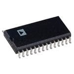
| 描述 | IC ADC 14BIT 400KSPS 5V 28-SSOP模数转换器 - ADC 5V SGL Supply 14-Bit 400 kSPS |
| 产品分类 | |
| 品牌 | Analog Devices |
| 产品手册 | |
| 产品图片 |
|
| rohs | 符合RoHS无铅 / 符合限制有害物质指令(RoHS)规范要求 |
| 产品系列 | 数据转换器IC,模数转换器 - ADC,Analog Devices AD7899ARSZ-1- |
| 数据手册 | |
| 产品型号 | AD7899ARSZ-1 |
| 产品目录页面 | |
| 产品种类 | 模数转换器 - ADC |
| 位数 | 14 |
| 供应商器件封装 | 28-SSOP |
| 信噪比 | 78 dB |
| 其它名称 | AD7899ARSZ1 |
| 分辨率 | 14 bit |
| 包装 | 管件 |
| 商标 | Analog Devices |
| 安装类型 | 表面贴装 |
| 安装风格 | SMD/SMT |
| 封装 | Tube |
| 封装/外壳 | 28-SSOP(0.209",5.30mm 宽) |
| 封装/箱体 | SSOP-28 |
| 工作温度 | -40°C ~ 85°C |
| 工作电源电压 | 5 V |
| 工厂包装数量 | 47 |
| 接口类型 | Parallel |
| 数据接口 | 并联 |
| 最大功率耗散 | 125 mW |
| 最大工作温度 | + 125 C |
| 最小工作温度 | - 55 C |
| 标准包装 | 47 |
| 电压参考 | Internal, External |
| 电压源 | 单电源 |
| 系列 | AD7899 |
| 结构 | SAR |
| 转换器数 | 1 |
| 转换器数量 | 1 |
| 转换速率 | 400 kS/s |
| 输入数和类型 | 1 个差分,双极 |
| 输入类型 | Single-Ended |
| 通道数量 | 1 Channel |
| 配用 | /product-detail/zh/EVAL-AD7899CBZ/EVAL-AD7899CBZ-ND/1858270 |
| 采样率(每秒) | 400k |


- 商务部:美国ITC正式对集成电路等产品启动337调查
- 曝三星4nm工艺存在良率问题 高通将骁龙8 Gen1或转产台积电
- 太阳诱电将投资9.5亿元在常州建新厂生产MLCC 预计2023年完工
- 英特尔发布欧洲新工厂建设计划 深化IDM 2.0 战略
- 台积电先进制程称霸业界 有大客户加持明年业绩稳了
- 达到5530亿美元!SIA预计今年全球半导体销售额将创下新高
- 英特尔拟将自动驾驶子公司Mobileye上市 估值或超500亿美元
- 三星加码芯片和SET,合并消费电子和移动部门,撤换高东真等 CEO
- 三星电子宣布重大人事变动 还合并消费电子和移动部门
- 海关总署:前11个月进口集成电路产品价值2.52万亿元 增长14.8%


PDF Datasheet 数据手册内容提取
a 5 V Single Supply 14-Bit 400 kSPS ADC AD7899 FEATURES FUNCTIONAL BLOCK DIAGRAM Fast (2.2(cid:2)s) 14-Bit ADC AVDD VREF VDRIVE 400 kSPS Throughput Rate 0.3(cid:2)s Track/Hold Acquisition Time 6k(cid:1) 2.5V Single Supply Operation STBY REFERENCE Selection of Input Ranges: (cid:3)10 V, (cid:3)5 V and (cid:3)2.5 V AD7899 + 0 V to 2.5 V and 0 V to 5 V – High-Speed Parallel Interface which Also Allows RD Interfacing to 3 V Processors TRACK/HOLD LPOoovwwer evProo-Slwtaaevgrie,n 8gP0 rMomtoeWdcet Ti,o y2np0 o(cid:2)nW A Tnyaplog Inputs VVIINNBA SSCIGANLIANLG 1A4-DBCIT OLUATTPCUHT DDBB013 Power-Down Mode via STBY Pin CS BUSY/EOC COCNOVNETRRSOIOLN ICNLTO/ECXKT CLINOTCK LOGIC SELECT CONVST CLKIN GND OPGND GENERAL DESCRIPTION PRODUCT HIGHLIGHTS The AD7899 is a fast, low-power, 14-bit A/D converter that 1. The AD7899 features a fast (2.2µs) ADC allowing through- operates from a single 5V supply. The part contains a 2.2µs put rates of up to 400 kSPS. successive-approximation ADC, a track/hold amplifier, 2.5 V 2. The AD7899 operates from a single 5V supply and con- reference, on-chip clock oscillator, signal conditioning circuitry, sumes only 80mW typ making it ideal for low power and and a high-speed parallel interface. The part accepts analog input portable applications. ranges of ±10V, ±5 V, ±2.5 V, 0 V to 2.5 V, and 0 V to 5 V. 3. The part offers a high-speed parallel interface. The interface Overvoltage protection on the analog input for the part allows can operate in 3 V and 5 V mode allowing for easy connec- the input voltage to be exceeded without damaging the parts. tion to 3 V or 5 V microprocessors, microcontrollers, and Speed of conversion can be controlled either by an internally digital signal processors. trimmed clock oscillator or by an external clock. 4. The part is offered in three versions with different analog A conversion start signal (CONVST) places the track/hold into input ranges. The AD7899-1 offers the standard industrial hold mode and initiates conversion. The BUSY/EOC signal ranges of ±10 V and ±5 V; the AD7899-2 offers a unipolar indicates the end of the conversion. range of 0 V to 2.5 or 0 V to 5 V, and the AD7899-3 has an Data is read from the part via a 14-bit parallel data bus using the input range of ±2.5 V. standard CS and RD signals. Maximum throughput for the AD7899 is 400 kSPS. The AD7899 is available in a 28-lead SOIC and SSOP packages. REV.A Information furnished by Analog Devices is believed to be accurate and reliable. However, no responsibility is assumed by Analog Devices for its use, nor for any infringements of patents or other rights of third parties that One Technology Way, P.O. Box 9106, Norwood, MA 02062-9106, U.S.A. may result from its use. No license is granted by implication or otherwise Tel: 781/329-4700 www.analog.com under any patent or patent rights of Analog Devices. Fax: 781/326-8703 © Analog Devices, Inc., 2001
AD7899–SPECIFICATIONS (VDD = 5 V (cid:3) 5%, AGND = DGND = 0 V, VREF = Internal. Clock = Internal, all specifications T to T and valid for V = 3 V (cid:3) 5% and 5 V (cid:3) 5% unless otherwise noted.) MIN MAX DRIVE A B S Parameter Version1 Version1 Version1 Unit Test Conditions/Comments SAMPLE AND HOLD –0.1 dB Full Power Bandwidth 500 500 500 kHz typ –3 dB Full Power Bandwidth 4.5 4.5 4.5 MHz typ Aperture Delay 20 20 20 ns max Aperture Jitter 25 25 25 ps typ DYNAMIC PERFORMANCE2 f = 100kHz, f = 400kSPS IN S AD7899-1 Signal to (Noise + Distortion) Ratio3 @ 25(cid:1)C 78 78 78 dB min T to T 78 78 77 dB min MIN MAX Total Harmonic Distortion3 –84 –84 –82 dB max Peak Harmonic or Spurious Noise3 –86 –86 –85 dB max AD7899-2 Signal to (Noise + Distortion) Ratio3 @ 25(cid:1)C 78 dB min T to T 77 dB min MIN MAX Total Harmonic Distortion3 –82 dB max Peak Harmonic or Spurious Noise3 –82 dB max AD7899-3 Signal to (Noise + Distortion) Ratio3 @ 25(cid:1)C 78 78 dB min T to T 77 77 dB min MIN MAX Total Harmonic Distortion3 –84 –84 dB max Peak Harmonic or Spurious Noise3 –86 –86 dB max Intermodulation Distortion3 fa = 49kHz, fb = 50kHz 2nd Order Terms –89 –89 –89 dB typ 3rd Order Terms –89 –89 –89 dB typ DC ACCURACY Resolution 14 14 14 Bits Relative Accuracy (INL)3 ±2 ±1.5 ±2 LSB max Differential Nonlinearity (DNL)3 ±1 ±1 ±1 LSB max No Missing Codes Guaranteed AD7899-1 Input Voltage Range ±5,±10 ±5,±10 Volts Input Current 0.8, 0.8 0.8, 0.8 mA max V = –5V and –10V Respectively IN Positive Gain Error3 ±10 ±8 ±12 LSB max Negative Gain Error3 ±10 ±8 ±12 LSB max Bipolar Zero Error ±12 ±8 ±12 LSB max AD7899-2 Input Voltage Range 0 to 2.5 Volts 0 to 5 Input Current 0.4, 800 µA max V = 2.5V, V = 5V IN IN Positive Gain Error3 ±14 LSB max Offset Error3 ±10 LSB max AD7899-3 Input Voltage Range ±2.5 ±2.5 Volts Input Current 0.8 0.8 mA max V = –2.5V IN Positive Gain Error3 ±14 ±12 LSB max Negative Gain Error3 ±14 ±12 LSB max Bipolar Zero Error ±14 ±12 LSB max REFERENCE INPUT/OUTPUT V IN Input Voltage Range 2.375/2.625 2.375/2.625 2.375/2.625 V /V 2.5V ± 5% REF MIN MAX V IN Input Capacitance4 10 10 10 pF max REF V OUT Output Voltage 2.5 2.5 2.5 Vnom REF V OUT Error @ 25(cid:1)C ±10 ±10 ±10 mV max REF V OUT Error T to T ±20 ±20 ±25 mV max REF MIN MAX V OUT Temperature Coefficient 25 25 25 ppm/(cid:1)C typ REF V OUT Output Impedance 6 6 6 kΩ typ See Reference Section REF –2– REV. A
AD7899 A B S Parameter Version1 Version1 Version1 Unit Test Conditions/Comments LOGIC INPUTS Input High Voltage, V V /2 + 0.4 V /2 + 0.4 V /2 + 0.4 V min V = 5V ± 5% INH DRIVE DRIVE DRIVE DD Input Low Voltage, V V /2 – 0.4 V /2 – 0.4 V /2 – 0.4 V max V = 5V ± 5% INL DRIVE DRIVE DRIVE DD Input Current, I ±10 ±10 ±10 µA max IN Input Capacitance, C 4 10 10 10 pF max IN LOGIC OUTPUTS Output High Voltage, V V – 0.4 V – 0.4 V – 0.4 V min I = 400µA OH DRIVE DRIVE DRIVE SOURCE Output Low Voltage, V 0.4 0.4 0.4 V max I = 1.6mA OL SINK DB13–DB0 High Impedance Leakage Current ±10 ±10 ±10 µA max Capacitance4 10 10 10 pF max Output Coding AD7899-1, AD7899-3 Two’s Complement AD7899-2 Straight (Natural) Binary CONVERSION RATE Conversion Time 2.2 2.2 2.2 µs max Track/Hold Acquisition Time2, 3 0.3 0.3 0.3 µs max Throughput Time 400 400 400 kSPS max POWER REQUIREMENTS V 5 5 5 V nom DD I DD Normal Mode 25 25 25 mA max Typically 16mA Standby Mode 20 20 20 µA max (5µA typ) Logic Inputs = 0V or V DD Power Dissipation Normal Mode 125 125 125 mW max Typically 80mW, V = 5 V DD Standby Mode 100 100 125 µW max NOTES 1Temperature Ranges are as follows : A, B Versions: –40(cid:1)C to +85(cid:1)C. S Version: –55°C to +125°C. 2 Performance measured through full channel (SHA and ADC). 3 See Terminology. 4Sample tested @ 25°C to ensure compliance. Specifications subject to change without notice. REV. A –3–
AD7899 TIMING CHARACTERISTICS1, 2 (V = 5 V (cid:3) 5%, AGND = DGND = 0 V, V = Internal, Clock = Internal; All specifications T DD REF MIN to T and valid for V = 3 V (cid:3) 5% and 5 V (cid:3) 5% unless otherwise noted.) MAX DRIVE A, B and S Parameter Versions Unit Test Conditions/Comments t 2.2 µs max Conversion Time, Internal Clock CONV 2.46 µs max CLKIN = 6.5 MHz t 0.3 µs max Acquisition Time ACQ t 120 ns min EOC Pulsewidth EOC 180 ns max t – External V 5 2 µs max STBY Rising Edge to CONVST Rising Edge WAKE-UP REF (See Standby Mode Operation) t 35 ns min CONVST Pulsewidth 1 t 70 ns min CONVST Rising Edge to BUSY Rising Edge 2 Read Operation t 0 ns min CS to RD Setup Time 3 t 0 ns min CS to RD Hold Time 4 t 35 ns min Read Pulsewidth 5 t 3 35 ns max Data Access Time after Falling Edge of RD, V = 5 V 6 DRIVE 40 ns max Data Access Time after Falling Edge of RD, V = 3 V DRIVE t 4 5 ns min Bus Relinquish Time after Rising Edge of RD 7 30 ns max t 0 ns min BUSY Falling Edge to RD Delay 8 External Clock t 0 ns min CLKIN to CONVST Rising Edge Setup Time 9 t 20 ns min CLKIN to CONVST Rising Edge Hold Time 10 t 100 ns min CONVST Rising Edge to CLK Falling Edge 11 NOTES 1 Sample tested at 25°C to ensure compliance. All input signals are measured with tr = tf = 1 ns (10% to 90% of V ) and timed from a voltage level of V /2. DRIVE DRIVE 2 See Figures 5, 6, 7, and 8. 3 Measured with the load circuit of Figure 1 and defined as the time required for an output to cross 0.8V or 2.0V. 4These times are derived from the measured time taken by the data outputs to change 0.5V when loaded with the circuit of Figure 1. The measured number is then extrapolated back to remove the effects of charging or discharging the 50 pF capacitor. This means that the times quoted in the timing characteristics are the true bus relinquish times of the part and as such are independent of external bus loading capacitances. 5 Refer to the Standby Mode Operation section. Specifications subject to change without notice. 1.6mA TO OUTPUT 1.6V PIN 50pF 400(cid:2)A Figure 1.Load Circuit for Access Time and Bus Relinquish Time –4– REV. A
AD7899 ABSOLUTE MAXIMUM RATINGS* SOIC Package, Power Dissipation . . . . . . . . . . . . . . . 450 mW (T = 25°C unless otherwise noted) θ Thermal Impedance . . . . . . . . . . . . . . . . . . . . . . . 95°C/W A JA V to AGND . . . . . . . . . . . . . . . . . . . . . . . . . –0.3V to +7 V Lead Temperature, Soldering VDD to DGND . . . . . . . . . . . . . . . . . . . . . . . . . –0.3V to +7 V Vapor Phase (60 sec) . . . . . . . . . . . . . . . . . . . . 215°C DD V to DGND . . . . . . . . . . . . . . . . . . . . . . . . . V + 0.3 V Infrared (15 sec) . . . . . . . . . . . . . . . . . . . . . . . . 220°C DRIVE DD Analog Input Voltage to AGND SSOP Package, Power Dissipation . . . . . . . . . . . . . . . 450 mW AD7899-1 (±10 V Range) . . . . . . . . . . . . . . . . . . . . ±18 V θJA Thermal Impedance . . . . . . . . . . . . . . . . . . . . . . . 95°C/W AD7899-1 (±5 V Range) . . . . . . . . . . . . . . . –9 V to +18 V Lead Temperature, Soldering AD7899-2 . . . . . . . . . . . . . . . . . . . . . . . . . . –1 V to +18 V Vapor Phase (60 sec) . . . . . . . . . . . . . . . . . . . . .215°C AD7899-3 . . . . . . . . . . . . . . . . . . . . . . . . . . –4 V to +18 V Infrared (15 sec) . . . . . . . . . . . . . . . . . . . . . . . . .220°C Reference Input Voltage to AGND . . . –0.3 V to VDD + 0.3 V *Stresses above those listed under Absolute Maximum Ratings may cause perma- Digital Input Voltage to DGND . . . . . –0.3 V to V + 0.3 V nent damage to the device. This is a stress rating only; functional operation of the DD Digital Output Voltage to DGND . . . . –0.3 V to V + 0.3 V device at these or any other conditions above those listed in the operational DD sections of this specification is not implied. Exposure to absolute maximum rating Operating Temperature Range conditions for extended periods may affect device reliability. Commercial (A, B Version) . . . . . . . . . . . –40°C to +85°C Military (S Version) . . . . . . . . . . . . . . . . . –55°C to +125°C Storage Temperature Range . . . . . . . . . . . –65°C to +150°C Junction Temperature . . . . . . . . . . . . . . . . . . . . . . . 150°C CAUTION ESD (electrostatic discharge) sensitive device. Electrostatic charges as high as 4000V readily WARNING! accumulate on the human body and test equipment and can discharge without detection. Although the AD7899 features proprietary ESD protection circuitry, permanent damage may occur on devices subjected to high-energy electrostatic discharges. Therefore, proper ESD precautions are recommended to avoid performance degradation or loss of functionality. ESD SENSITIVE DEVICE ORDERING GUIDE Relative Temperature Package Package Model Input Ranges Accuracy Range Description Option AD7899AR-1 ±5V, ±10V ±2 LSB –40(cid:1)C to +85(cid:1)C Small Outline R-28 AD7899BR-1 ±5V, ±10V ±1.5 LSB –40(cid:1)C to +85(cid:1)C Small Outline R-28 AD7899SR-1 ±5V, ±10V ±2 LSB –55(cid:1)C to +125(cid:1)C Small Outline R-28 AD7899AR-2 0V to 5V, 0V to 2.5V ±2 LSB –40(cid:1)C to +85(cid:1)C Small Outline R-28 AD7899AR-3 ±2.5V ±2 LSB –40(cid:1)C to +85(cid:1)C Small Outline R-28 AD7899BR-3 ±2.5V ±1.5 LSB –40(cid:1)C to +85(cid:1)C Small Outline R-28 AD7899ARS-1 ±5V, ±10V ±2 LSB –40(cid:1)C to +85(cid:1)C Shrink Small Outline RS-28 AD7899ARS-2 0V to 5V, 0V to 2.5V ±2 LSB –40(cid:1)C to +85(cid:1)C Shrink Small Outline RS-28 AD7899ARS-3 ±2.5V ±2 LSB –40(cid:1)C to +85(cid:1)C Shrink Small Outline RS-28 REV. A –5–
AD7899 PIN FUNCTION DESCRIPTIONS Pin No. Mnemonic Description 1 V Reference Input/Output. This pin is provides access to the internal reference (2.5 V ± 20 mV) and REF also allows the internal reference to be overdriven by an external reference source (2.5 V ± 5%). A 0.1 µF decoupling capacitor should be connected between this pin and GND. 2, 6 GND Ground Pin. This pin should be connected to the system’s analog groundplane. 3, 4 V , V Analog Inputs. See Analog Input Section. INB INA 5 V Positive Supply Voltage, 5.0 V ± 5%. DD 7–13 DB13–DB7 Data Bit 13 is the MSB, followed by Data Bit 12 to Data Bit 7. Three-state outputs. 14 OPGND Output Driver Ground. This is the ground pin of the output drivers for D13 to D0 and BUSY/EOC. It should be connected to the system’s analog ground plane. 15 V This pin provides the positive supply voltage for the digital inputs and outputs. It is normally tied to V DRIVE DD but may also be powered by a 3 V ± 10% supply which allows the inputs and outputs to be interfaced to 3 V processors and DSPs. V should be decoupled with a 0.1 µF capacitor to GND. DRIVE 16–22 DB6–DB0 Data Bit 6 to Data Bit 0. Three-state Outputs. 23 BUSY/EOC BUSY/EOC Output. Digital output pin used to signify that a conversion is in progress or that a conversion has finished. The function of the BUSY/EOC is determined by the state of CONVST at the end of con- version. See the Timing and Control Section. 24 RD Read Input. Active low logic input which is used in conjunction with CS low to enable the data outputs. 25 CS Chip Select Input. Active low logic input. The device is selected when this input is active. 26 CONVST Convert Start Input. Logic Input. A low to high transition on this input puts the track/hold into hold mode and starts conversion. 27 CLKIN Conversion Clock Input. CLKIN is an externally applied clock which allows the user to control the conversion rate of the AD7899. If the CLKIN input is high on the rising edge of CONVST an externally applied clock will be used as the conversion clock. If the CLKIN is low on the rising edge of CONVST the internal laser-trimmed oscillator is used as the conversion clock. Each conversion needs sixteen clock cycles in order for the conversion to be completed. The externally applied clock should have a duty cycle no greater than 60/40. The CLKIN pin can be tied to GND if an external clock is not required. 28 STBY Standby Mode Input. Logic input which is used to put the device into the power save or standby mode. The STBY input is high for normal operation and low for standby operation. PIN CONFIGURATION SOIC/SSOP VREF 1 28 STBY GND 2 27 CLKIN VINB 3 26 CONVST VINA 4 25 CS VDD 5 24 RD GND 6 23 BUSY/EOC AD7899 DB13 7 TOP VIEW 22 DB0 DB12 8 (Not to Scale) 21 DB1 DB11 9 20 DB2 DB10 10 19 DB3 DB9 11 18 DB4 DB8 12 17 DB5 DB7 13 16 DB6 OPGND 14 15 VDRIVE –6– REV. A
AD7899 TERMINOLOGY and third order terms are specified separately. The calculation Signal to (Noise + Distortion) Ratio of the intermodulation distortion is as per the THD speci- This is the measured ratio of signal to (noise + distortion) at the fication where it is the ratio of the rms sum of the individual output of the A/D converter. The signal is the rms amplitude of distortion products to the rms amplitude of the fundamental the fundamental. Noise is the rms sum of all nonfundamental expressed in dBs. signals up to half the sampling frequency (f /2), excluding dc. S Differential Nonlinearity The ratio is dependent upon the number of quantization levels This is the difference between the measured and the ideal in the digitization process; the more levels, the smaller the quan- 1 LSB change between any two adjacent codes in the ADC. tization noise. The theoretical signal to (noise + distortion) ratio for an ideal N-bit converter with a sine wave input is given by: Positive Gain Error (AD7899-1, AD7899-3) This is the deviation of the last code transition (01...110 to Signal to (Noise + Distortion) = (6.02N + 1.76) dB 01...111) from the ideal 4 × V – 3/2 LSB (AD7899 at REF Thus for a 14-bit converter, this is 86.04dB. ±10 V), 2 × V – 3/2 LSB (AD7899 at ±5 V range) or V REF REF – 3/2 LSB (AD7899 at ±2.5 V range) after the Bipolar Offset Total Harmonic Distortion Error has been adjusted out. Total harmonic distortion (THD) is the ratio of the rms sum of harmonics to the fundamental. For the AD7899 it is defined Positive Gain Error (AD7899-2) This is the deviation of the last code transition (11...110 to as:THD(dB)=20log V22 +V32 +V42 +V52 +V62 11...111) from the ideal 2 × VREF – 3/2 LSB (AD7899 at V ±10 V), 2 × V – 3/2 LSB (AD7899 at 0 V to 5 V range) or 1 REF V – 3/2 LSB (AD7899 at 0 V to 2.5 V range) after the Uni- where V is the rms amplitude of the fundamental and V , V , REF 1 2 3 polar Offset Error has been adjusted out. V , and V are the rms amplitudes of the second through the 4 5 fifth harmonics. Unipolar Offset Error (AD7899-2) This is the deviation of the first code transition (00...00 to Peak Harmonic or Spurious Noise 00...01) from the ideal AGND +1/2 LSB Peak harmonic or spurious noise is defined as the ratio of the rms value of the next largest component in the ADC output Bipolar Zero Error (AD7899-1, AD7899-2) spectrum (up to f /2 and excluding dc) to the rms value of the This is the deviation of the midscale transition (all 0s to all 1s) S fundamental. Normally, the value of this specification is deter- from the ideal AGND – 1/2 LSB. mined by the largest harmonic in the spectrum, but for parts Negative Gain Error (AD7899-1, AD7899-3) where the harmonics are buried in the noise floor, it will be a This is the deviation of the first code transition (10...000 to noise peak. 10...001) from the ideal –4 × V + 1/2 LSB (AD7899 at REF ±10 V), –2 × V + 1/2 LSB (AD7899 at ±5 V range) or –V Intermodulation Distortion REF REF With inputs consisting of sine waves at two frequencies, fa and + 1/2 LSB (AD7899 at ±2.5 V range) after Bipolar Zero Error fb, any active device with nonlinearities will create distortion has been adjusted out. products at sum and difference frequencies of mfa ± nfb where Track/Hold Acquisition Time m, n = 0, 1, 2, 3, etc. Intermodulation terms are those for which Track/Hold acquisition time is the time required for the output neither m nor n are equal to zero. For example, the second order of the track/hold amplifier to reach its final value, within ±1/2 LSB, terms include (fa + fb) and (fa – fb), while the third order terms after the end of conversion (the point at which the track/hold include (2fa + fb), (2fa – fb), (fa + 2fb) and (fa – 2fb). returns to track mode). It also applies to situations where there The AD7899 is tested using two input frequencies. In this case, the is a step input change on the input voltage applied to the selected second and third order terms are of different significance. The VINA/VINB input of the AD7899. It means that the user must wait second order terms are usually distanced in frequency from the for the duration of the track/hold acquisition time after the end original sine waves while the third order terms are usually at a of conversion or after a step input change to VINA/VINB before frequency close to the input frequencies. As a result, the second starting another conversion, to ensure that the part operates to specification. REV. A –7–
AD7899 CONVERTER DETAILS external CONVST signal and the track/hold actually going into The AD7899 is a high-speed, low-power, 14-bit A/D converter hold) is typically 15ns and, more importantly, is well matched that operates from a single 5V supply. The part contains a from device to device. It allows multiple AD7899s to sample 2.2 µs successive-approximation ADC, track/hold amplifier, an more than one channel simultaneously. At the end of a conversion, internal 2.5V reference and a high-speed parallel interface. The the part returns to its tracking mode. The acquisition time of part accepts an analog input range of ±10 V or ±5 V (AD7899-1), the track/hold amplifier begins at this point. 0 V to 2.5 V or 0 V to 5 V (AD7899-2) and ±2.5 V (AD7899-3). Reference Section Overvoltage protection on the analog inputs for the part allows The AD7899 contains a single reference pin, labelled V , the input voltage to go to ±18 V (AD7899-1 with ±10 V input REF which either provides access to the part’s own 2.5V reference or range), –9 V to +18 V (AD7899-1 with ±5 V input range), –1 V allows an external 2.5V reference to be connected to provide to +18 V (AD7899-2) and –4 V to +18 V (AD7899-3) without the reference source for the part. The part is specified with a causing damage. 2.5V reference voltage. A conversion is initiated on the AD7899 by pulsing the CONVST To use the internal reference as the reference source for the input. On the rising edge of CONVST, the on-chip track/hold is AD7899, simply connect a 0.1µF capacitor from the V pin placed into hold and the conversion is started. The BUSY/EOC REF to AGND. The voltage that appears at this pin is internally output signal is triggered high on the rising edge of CONVST buffered before being applied to the ADC. If this reference is and will remain high for the duration of the conversion sequence. required for use external to the AD7899, it should be buffered, The conversion clock for the part is generated internally using a as the part has a FET switch in series with the reference output laser-trimmed clock oscillator circuit. There is also the option of resulting in a source impedance for this output of 6 kΩ nominal. using an external clock. An external noncontinuous clock is applied The tolerance on the internal reference is ±10mV at 25°C with to the CLKIN pin. If, on the rising edge of CONVST, this input a typical temperature coefficient of 25ppm/°C and a maximum is high, the external clock will be used. The external clock should error over temperature of ±20 mV. not start until 100 ns after the rising edge of CONVST. The optimum throughput is obtained by using the internally gener- If the application requires a reference with a tighter tolerance or the AD7899 needs to be used with a system reference, the user ated clock—see Using an External Clock. The BUSY/EOC signal indicates the end of the conversion, and at this time the Track and has the option of connecting an external reference to this VREF pin. The external reference will effectively overdrive the internal Hold returns to tracking mode. The conversion results can be reference and thus provide the reference source for the ADC. read at the end of the conversion (indicated by BUSY/EOC going low) via a 14-bit parallel data bus with standard CS and RD The reference input is buffered before being applied to the ADC signals—see Timing and Control. with the maximum input current of ±100µA. Suitable reference sources for the AD7899 include the AD680, AD780, REF192, Conversion time for the AD7899 is 2.2 µs and the track/hold and REF43 precision 2.5V references. acquisition time is 0.3µs. To obtain optimum performance from the part, the read operation should not occur during a conversion Analog Input Section The AD7899 is offered as three part types, the AD7899-1 where or during the 150 ns prior to the next CONVST rising edge. the input can be configured for ±10 V or a ±5 V input voltage This allows the part to operate at throughput rates up to 400 kHz and achieve data sheet specifications. range, the AD7899-2 where the input can be configured for 0 V to 5 V or a 0 V to 2.5 V input voltage range and the AD7899-3 which handles input voltage range ±2.5 V. The amount of current CIRCUIT DESCRIPTION flowing into the analog input will depend on the analog input Track/Hold Section The track/hold amplifier on the AD7899 allows the ADCs to range and the analog input voltage. The maximum current flows accurately convert an input sine wave of full-scale amplitude to when negative full-scale is applied. 14-bit accuracy. The input bandwidth of the track/hold is greater AD7899-1 than the Nyquist rate of the ADC even when the ADC is oper- Figure 2 shows the analog input section of the AD7899-1. The ated at its maximum throughput rate of 400 kSPS (i.e., the input can be configured for ±5 V or ±10 V operation on the track/hold can handle input frequencies in excess of 200 kHz). AD7899-1. For ±5 V operation, the V and V inputs are INA INB The track/hold amplifier’s acquire input signals to 14-bit tied together and the input voltage is applied to both. For ±10 V accuracy in less than 300 ns The operation of the track/hold is operation, the VINB input is tied to AGND and the input voltage essentially transparent to the user. The track/hold amplifier is applied to the VINA input. The VINA and VINB inputs are sym- samples the input channel on the rising edge of CONVST. The metrical and fully interchangeable. aperture time for the track/hold (i.e., the delay time between the –8– REV. A
AD7899 AD7899-2 AD7899-1 Figure 3 shows the analog input section of the AD7899-2. Each 2.5V input can be configured for 0 V to 5 V operation or 0 V to 2.5 V REFERENCE operation. For 0 V to 5 V operation, the V input is tied to INB GND and the input voltage is applied to the V input. For 6k(cid:1) INA 0 V to 2.5 V operation, the V and V inputs are tied together INA INB TO ADC and the input voltage is applied to both. The V and V REFERENCE INA INB VREF CIRCUITRY inputs are symmetrical and fully interchangeable. R1 For the AD7899-2, R1 = 4 kΩ and R2 = 4 kΩ. Once again, the VINA R2 TO INTERNAL designed code transitions occur on successive integer LSB values. COMPARATOR Output coding is straight (natural) binary with 1 LSB = FSR/ TRACK/HOLD 16384 = 2.5 V/16384 = 0.153 mV, and 5 V/16384 = 0.305 mV, R3 for the 0 to 2.5 V and the 0 to 5 V options respectively. Table VINB II shows the ideal input and output transfer function for the R4 AD7899-2. GND AD7899-2 Figure 2.AD7899-1 Analog Input Structure 2.5V For the AD7899-1, R1 = 4 kΩ, R2 = 16 kΩ, R3 = 16 kΩ and REFERENCE R4 = 8 kΩ. The resistor input stage is followed by the high input impedance stage of the track/hold amplifier. 6k(cid:1) The designed code transitions take place midway between suc- TO ADC REFERENCE cessive integer LSB values (i.e., 1/2 LSB, 3/2 LSBs, 5/2 LSBs VREF CIRCUITRY etc.) LSB size is given by the formula, 1 LSB = FSR/16384. For the ±5 V range, 1 LSB = 10 V/16384 = 610.4 µV. For the ±10 V R1 range, 1 LSB = 20 V/16384 = 1.22 mV. Output coding is VINA TCOO MINPTAERRANTAOLR two’s complement binary with 1 LSB = FSR/16384. The ideal TRACK/HOLD input/output transfer function for the AD7899-1 is shown in R2 Table I. VINB Table I. Ideal Input/Output Code Table for the AD7899-1 Digital Output Figure 3.AD7899-2 Analog Input Structure Analog Input1 Code Transition Table II. Ideal Input/Output Code Table for the AD7899-2 +FSR/2 – 3/2 LSB2 011 . . . 110 to 011 . . . 111 +FSR/2 – 5/2 LSB 011 . . . 101 to 011 . . . 110 Digital Output +FSR/2 – 7/2 LSB 011 . . . 100 to 011 . . . 101 Analog Input1 Code Transition GND + 3/2 LSB 000 . . . 001 to 000 . . . 010 +FSR – 3/2 LSB2 111 . . . 110 to 111 . . . 111 GND + 1/2 LSB 000 . . . 000 to 000 . . . 001 +FSR – 5/2 LSB 111 . . . 101 to 111 . . . 110 GND – 1/2 LSB 111 . . . 111 to 000 . . . 000 +FSR – 7/2 LSB 111 . . . 100 to 111 . . . 101 GND – 3/2 LSB 111 . . . 110 to 111 . . . 111 GND + 5/2 LSB 000 . . . 010 to 000 . . . 011 –FSR/2 + 5/2 LSB 100 . . . 010 to 100 . . . 011 GND + 3/2 LSB 000 . . . 001 to 000 . . . 010 –FSR/2 + 3/2 LSB 100 . . . 001 to 100 . . . 010 GND + 1/2 LSB 000 . . . 000 to 000 . . . 001 –FSR/2 + 1/2 LSB 100 . . . 000 to 100 . . . 001 NOTES 1FSR is Full-Scale Range and is 0 to 2.5 V and 0 to 5 V for AD7899-2 with V NOTES REF 1FSR is full-scale range and is 20 V for the ±10 V range and 10 V for the ±5 V = 2.5 V. 21 LSB = FSR/16384 and is 0.153 mV (0 to 2.5 V) and 0.305 mV (0 to 5 V) for range, with V = 2.5 V. 21 LSB = FSR/R1E6F384 = 1.22 mV (±10 V – AD7899-1) and 610.4 µV (±5 V – AD7899-2 with VREF = 2.5 V. AD7899-1) with V = 2.5 V. REF REV. A –9–
AD7899 AD7899-3 TIMING AND CONTROL Figure 4 shows the analog input section of the AD7899-3. The Starting a Conversion analog input range is ±2.5 V on the V input. The V input The conversion is initiated by applying a rising edge to the INA INB can be left unconnected but if it is connected to a potential then CONVST signal. This places the track/hold into hold mode and that potential must be GND. starts the conversion. The status of the conversion is indicated by the dual function signal BUSY/EOC. The AD7899 can operate in two conversion modes, EOC (End Of Conversion) mode and AD7899-3 BUSY mode. The operating mode is determined by the state of 2.5V CONVST at the end of the conversion. REFERENCE Selecting a Conversion Clock 6k(cid:1) The AD7899 has an internal laser trimmed oscillator which can be used to control the conversion process. Alternatively an external TO ADC REFERENCE clock source can be used to control the conversion process. The VREF CIRCUITRY highest external clock frequency allowed is 6.5 MHz. This means R1 a conversion time of 2.46 µs compared to 2.2 µs using the inter- VINA R2 TO INTERNAL nal clock. However in some instances it may be useful to use an COMPARATOR external clock when high throughput rates are not required. For TRACK/HOLD example two or more AD7899s may be synchronized by using the same external clock for all devices. In this way there is no VINB latency between output logic signals due to differences in the frequency of the internal clock oscillators. On the rising edge of CONVST the AD7899 will examine the Figure 4.AD7899-3 Analog Input Structure status of the CLKIN pin. If this pin is low it will use the internal For the AD7899-3, R1 = 4 kΩ and R2 = 4 kΩ. The resistor laser trimmed oscillator as the conversion clock. If the CLKIN pin input stage is followed by the high input impedance stage of the is high the AD7899 will wait for an external clock to be supplied track/hold amplifier. to this pin which will then be used as the conversion clock. The first falling edge of the external clock should not happen for at The designed code transitions take place midway between suc- least 100 ns after the rising edge of CONVST to ensure correct cessive integer LSB values (i.e., 1/2 LSB, 3/2 LSBs, 5/2 LSBs operation. Figure 5 shows how the BUSY/EOC output is synchro- etc.) LSB size is given by the formula, 1 LSB = FSR/16384. nized to the CLKIN signal. Each conversion requires 16 clocks. Output coding is two’s complement binary with 1 LSB = FSR/ The result of the conversion is transferred to the output data 16384 = 5 V/16384 = 610.4 µV. The ideal input/output transfer register on the falling edge of the 15th clock cycle. When the function for the AD7899-3 is shown in Table III. internal clock is selected the status of the CLKIN pin is free to change during conversion but the CLKIN setup and hold times Table III. Ideal Input/Output Code Table for the AD7899-3 must be observed in order to ensure that the correct conversion clock is used. The CLKIN pin can also be tied low permanently if Digital Output Analog Inputl Code Transition the internal conversion clock is to be used. +FSR/2 – 3/2 LSB2 011 . . . 110 to 011 . . . 111 t 9 +FSR/2 – 5/2 LSB 011 . . . 101 to 011 . . . 110 1 2 3 4 5 6 7 8 910111213141516 +FSR/2 – 7/2 LSB 011 . . . 100 to 011 . . . 101 CLKIN t GND + 3/2 LSB 000 . . . 001 to 000 . . . 010 11 GND + 1/2 LSB 000 . . . 000 to 000 . . . 001 CONVST GND – 1/2 LSB 111 . . . 111 to 000 . . . 000 GND – 3/2 LSB 111 . . . 110 to 111 . . . 111 BUSY/EOC –FSR/2 + 5/2 LSB 100 . . . 010 to 100 . . . 011 –FSR/2 + 3/2 LSB 100 . . . 001 to 100 . . . 010 –FSR/2 + 1/2 LSB 100 . . . 000 to 100 . . . 001 RD NOTES 1FSR is full-scale range is 5 V, with V = 2.5 V CS REF 21 LSB = FSR/16384 = 610.4 µV (±2.5 V – AD7899-3) with V = 2.5 V. REF Figure 5.Using an External Clock –10– REV. A
AD7899 t 10 t 9 CLKIN t t 1 ACQ CONVST tEOC QUIET t t TIME 2 8 BUSY/EOC t CONV t RD 5 t t 3 4 CS THREE-STATE THREE-STATE DATA t6 t7 Figure 6.Conversion Sequence Timing Diagram (EOC Mode) t 10 t 9 CLKIN t t 1 ACQ CONVST t 8 QUIET BUSY/EOC TIME t CONV t RD 5 t t CS 3 4 THREE-STATE THREE-STATE DATA t6 t7 Figure 7.Conversion Sequence Timing Diagram (BUSY Mode) EOC Mode Continuous Conversion Mode The CONVST signal is normally high. Pulsing the CONVST low When the AD7899 is used with an external clock, connecting will initiate a conversion on its rising edge. The state of the the CLKIN and CONVST signals together will cause the AD7899 CONVST signal is checked at the end of conversion. Since the to continuously perform conversions. As each conversion com- CONVST will be high when this happens the AD7899 BUSY/ pletes the BUSY/EOC pin will pulse low for one clock period EOC pin will take on its EOC function and bring the BUSY/EOC (EOC function) indicating that the conversion result is available. line low for one clock period before returning high again. In this Figure 8 shows the timing and control sequence of the AD7899 mode the EOC can be tied to the RD and CS signals to allow in Continuous Conversion Mode. automatic reading of the conversion result if required. The timing Reading Data from the AD7899 diagram for operation in EOC mode is shown in Figure 6. Data is read from the part via a 14-bit parallel data bus with BUSY Mode standard CS and RD signals. The CS and RD inputs are inter- The CONVST signal is normally low. Pulsing the CONVST nally gated to enable the conversion result onto the data bus. high will initiate a conversion on its rising edge. The state of the The data lines DB0 to DB13 leave their high impedance state CONVST signal is checked at the end of conversion. Since the when both CS and RD are logic low. Therefore CS may be CONVST will be low when this happens the AD7899 BUSY/ permanently tied logic low and the RD signal used to access the EOC pin will take on its BUSY function will bring BUSY/EOC conversion result if required. Figures 6 and 7 show a timing low, indicating that the conversion is complete. BUSY/EOC will specification called “Quiet Time.” This is the amount of time remain low until the next rising edge of CONVST where BUSY/ which should be left after a read operation and before the next EOC returns high. The timing diagram for operation in BUSY conversion is initiated. The quiet time depends heavily on data mode is shown in Figure 7. bus capacitance but a figure of 50 ns to 100 ns is typical, with a worst case figure of 150 ns. REV. A –11–
AD7899 1 2 3 4 5 6 7 8 9 10 11 12 13 14 15 16 CONVST/ CLKIN EOC START OF NEW CONVERSION CONVERSION (INPUT SAMPLED) COMPLETE Figure 8.Continuous Conversion Mode Standby Mode Operation Signal-to-Noise Ratio (SNR) The AD7899 has a Standby Mode whereby the device can be SNR is the measured signal-to-noise ratio at the output of the placed in a low current consumption mode (5 µA typ). The ADC. The signal is the rms magnitude of the fundamental. AD7899 is placed in Standby by bringing the logic input STBY Noise is the rms sum of all the nonfundamental signals up to low. The AD7899 can be powered again up for normal opera- half the sampling frequency (f /2) excluding dc. SNR is dependent S tion by bringing STBY logic high. The output data buffers are upon the number of quantization levels used in the digitization still operational while the AD7899 is in Standby. This means process; the more levels, the smaller the quantization noise. The the user can still continue to access the conversion results while theoretical signal to noise ratio for a sine wave input is given by the AD7899 is in standby. This feature can be used to reduce SNR = (6.02N + 1.76) dB (1) the average power consumption in a system using low throughput where N is the number of bits. rates. To reduce the average power consumption, the AD7899 can be placed in standby at the end of each conversion sequence Thus for an ideal 14-bit converter, SNR = 86.04 dB. and taken out of standby again prior to the start of the next Figure 9 shows a histogram plot for 8192 conversions of a dc conversion sequence. The time it takes the AD7899 to come out input using the AD7899 with 5 V supply. The analog input was of standby is called the “wake up” time. This wake-up time will set at the center of a code transition. It can be seen that most of limit the maximum throughput rate at which the AD7899 can the codes appear in one output bin, indicating very good noise be operated when powering down between conversions. When performance from the ADC. the AD7899 is used with the internal reference, the reference capacitor will begin to discharge during standby. The voltage 7000 remaining on the capacitor at wake-up time will depend upon the standby time and hence affect the wake-up time. The mini- 6000 mum wake-up time is typically 2 µs. The maximum wake-up time will be when the AD7899 has been in standby long enough 5000 for the reference capacitor to fully discharge. The wake-up time in this case will typically be 15 ms. The AD7899 will wake up in 4000 approximately 1 µs when using an external reference, regardless of sleep time. 3000 When operating the AD7899 in a Standby mode between con- 2000 versions, the power savings can be significant. For example, with a throughput rate of 10 kSPS and an external reference, the 1000 AD7899 will be powered up for 4.2 µs out of every 100 µs (2 µs for wake-up time and 2.2 µs for conversion time). Therefore, the 0 average power consumption drops to 80 mW × 4.2% or approxi- Figure 9.Histogram of 8192 Conversions of a DC Input mately 3.36 mW. The output spectrum from the ADC is evaluated by applying a AD7899 DYNAMIC SPECIFICATIONS sine wave signal of very low distortion to the analog input. A The AD7899 is specified and 100% tested for dynamic perfor- Fast Fourier Transform (FFT) plot is generated from which the mance specifications as well as traditional dc specifications such SNR data can be obtained. Figure 10 shows a typical 4096 point as Integral and Differential Nonlinearity. These ac specifications FFT plot of the AD7899 with an input signal of 100 kHz and a are required for the signal processing applications such as phased sampling frequency of 400 kHz. The SNR obtained from this array sonar, adaptive filters, and spectrum analysis. These appli- graph is 80.5 dB. It should be noted that the harmonics are cations require information on the ADC’s effect on the spectral taken into account when calculating the SNR. content of the input signal. Hence, the parameters for which the AD7899 is specified include SNR, harmonic distortion, inter- modulation distortion, and peak harmonics. These terms are discussed in more detail in the following sections. –12– REV. A
AD7899 second and third order terms are specified separately. The cal- 0 culation of the intermodulation distortion is as per the THD specification where it is the ratio of the rms sum of the indi- –20 vidual distortion products to the rms amplitude of the fundamental fs = 400kHz –40 fIN = 100kHz expressed in dBs. In this case, the input consists of two, equal SNR = 80.5dB amplitude, low distortion sine waves. Figure 12 shows a typical –60 IMD plot for the AD7899. B d –80 0 –100 –20 –120 –40 –140 –60 0 50000 100000 150000 200000 FREQUENCY – Hz dB –80 Figure 10.FFT Plot Effective Number of Bits –100 The formula given in Equation 1 relates the SNR to the number of bits. Rewriting the formula, as in Equation 2, it is possible to –120 obtain a measure of performance expressed in effective number of bits (N). –1400 50000 100000 150000 200000 FREQUENCY – Hz SNR−1.76 N = (2) Figure 12.IMD Plot 6.02 The effective number of bits for a device can be calculated directly AC Linearity Plots The plots in Figure 13 show typical DNL and INL for the from its measured SNR. Figure 11 shows a typical plot of effec- AD7899. tive number of bits versus frequency for an AD7899. 1.00 14 13 –55(cid:4)C 12 11 +25(cid:4)C 0.50 10 9 B S B 8 +125(cid:4)C – L 0 NO 7 NL E 6 D 5 4 –0.50 3 2 1 –1.00 0 0 2000 4000 6000 8000 10000 12000 14000 16000 0 100 1000 10000 ADC – Code INPUT FREQUENCY – kHz 1.00 Figure 11.Effective Numbers of Bits vs. Frequency Intermodulation Distortion With inputs consisting of sine waves at two frequencies, fa and 0.50 fb, any active device with nonlinearities will create distortion products at sum and difference frequencies of mfa ± nfb where B S m, n = 0, 1, 2, 3 . . ., etc. Intermodulation terms are those for – L 0 which neither m nor n are equal to zero. For example, the sec- L N I ond order terms include (fa + fb) and (fa – fb) while the third order terms include (2fa + fb), (2fa – fb), (fa + 2fb) and (fa – 2fb). –0.50 The AD7899 is tested using two input frequencies. In this case the second and third order terms are of different significance. The second order terms are usually distanced in frequency from –1.00 the original sine waves while the third order terms are usually at 0 2000 4000 6000 8000 10000 12000 14000 16000 a frequency close to the input frequencies. As a result, the ADC – Code Figure 13.Typical DNL and INL Plots REV. A –13–
AD7899 MICROPROCESSOR INTERFACING AD7899–TMS320C5x Interface The high-speed parallel interface of the AD7899 allows easy Figure 15 shows an interface between the AD7899 and the interfacing to most DSPs and microprocessors. The AD7899 TMS320C5x. As with the previous interfaces, conversion can be interface of the AD7899 consists of the data lines (DB0 to DB13), initiated from the TMS320C5x or from an external source and CS, RD, and BUSY/EOC. the processor is interrupted when the conversion sequence is completed. The CS signal to the AD7899 derived from the DS AD7899–ADSP-21xx Interface signal and a decode of the address bus. This maps the AD7899 Figure 14 shows an interface between the AD7899 and the into external data memory. The RD signal from the TMS320 is ADSP-21xx. The CONVST signal can be generated by the used to enable the ADC data onto the data bus. The AD7899 has ADSP-21xx or from some other external source. Figure 14 shows a fast parallel bus so there are no wait state requirements. The the CS being generated by a combination of the DMS signal and following instruction is used to read the conversion results from the address bus of the ADSP-21xx. In this way the AD7899 is the AD7899: mapped into the data memory space of the ADSP-21xx. IN D,ADC The AD7899 BUSY/EOC line provides an interrupt to the ADSP-21xx when the conversion is complete. The conversion where D is Data Memory address and ADC is the AD7899 result can then be read from the AD7899 using a read operation. address. The AD7899 is read using the following instruction MR0 = DM(ADC) TMS320C5x where MR0 is the ADSP-21xx MR0 register and ADC is the AD7899 address. ADDRESS A0–A13 DECODE DS CS ADSP-21xx RD RD VIN ADDRESS A0–A13 DECODE DMS DB0–DB13 D0–D13 CS AD7899 RD RD VIN BUSY/EOC INTn DB0–DB13 D8–D21 CONVST PA0 AD7899 Figure 15.AD7899–TMS320C5x Interface BUSY/EOC IRQn CONVST DT1/F0 Figure 14.AD7899–ADSP-21xx Interface –14– REV. A
AD7899 OUTLINE DIMENSIONS Dimensions shown in inches and (mm). 28-Lead Small Outline (R-28) 0.7125 (18.10) 0.6969 (17.70) 28 15 0.2992 (7.60) 0.2914 (7.40) 0.4193 (10.65) 1 14 0.3937 (10.00) PIN 1 0.1043 (2.65) 0.0291 (0.74) 0.0926 (2.35) 0.0098 (0.25)(cid:5) 45(cid:4) 8(cid:4) 00..00101480 ((00..3100)) 0(B.10.S52C070) 00..00119328 ((00..4395)) SPELAANTIENG 00..00102951 ((00..3223)) 0(cid:4) 00..00510507 ((10..2470)) 28-Lead Shrink Small Outline (RS-28) 0.407 (10.34) 0.397 (10.08) 28 15 0.311 (7.9)0.301 (7.64) 0.212 (5.38)0.205 (5.21) 1 14 0.078 (1.98)PIN 1 0.07 (1.79) 0.068 (1.73) 0.066 (1.67) 8° 0.03 (0.762) 00..000082 ((00..200530))0(B.00.S26C556) 00..001150 ((00..3285)) SEPALTAINNGE 00..000095 ((00..212297))0° 0.022 (0.558) AD7899–Revision History Location Page Data Sheet changed from REV. 0 to REV. A. Edit to Timing page heading . . . . . . . . . . . . . . . . . . . . . . . . . . . . . . . . . . . . . . . . . . . . . . . . . . . . . . . . . . . . . . . . . . . . . . . . . . . . . . 4 Edit to Converter Details section . . . . . . . . . . . . . . . . . . . . . . . . . . . . . . . . . . . . . . . . . . . . . . . . . . . . . . . . . . . . . . . . . . . . . . . . . . . 8 Edit to Figure 14 . . . . . . . . . . . . . . . . . . . . . . . . . . . . . . . . . . . . . . . . . . . . . . . . . . . . . . . . . . . . . . . . . . . . . . . . . . . . . . . . . . . . . . 14 REV. A –15–
A) 1( 0 6/ – 0 – 5 6 3 1 0 C A. S. U. N D I E T N RI P –16–
Mouser Electronics Authorized Distributor Click to View Pricing, Inventory, Delivery & Lifecycle Information: A nalog Devices Inc.: AD7899SR-1 AD7899SRZ-1 AD7899ARS-1 AD7899ARSZ-3REEL AD7899ARSZ-2 AD7899ARSZ-1 AD7899BRZ- 1 AD7899ARZ-2REEL AD7899BR-1 AD7899ARZ-2 AD7899ARSZ-1REEL7 AD7899ARZ-1REEL AD7899ARZ-3 AD7899ARSZ-1REEL AD7899AR-3 AD7899ARZ-1 AD7899ARSZ-2REEL AD7899ARSZ-3 AD7899BRZ-3 AD7899AR-1