ICGOO在线商城 > 集成电路(IC) > 数据采集 - 模数转换器 > ADS8326IDGKT
 Datasheet下载
- 型号: ADS8326IDGKT
- 制造商: Texas Instruments
- 库位|库存: xxxx|xxxx
- 要求:
| 数量阶梯 | 香港交货 | 国内含税 |
| +xxxx | $xxxx | ¥xxxx |
查看当月历史价格
查看今年历史价格
ADS8326IDGKT产品简介:
ICGOO电子元器件商城为您提供ADS8326IDGKT由Texas Instruments设计生产,在icgoo商城现货销售,并且可以通过原厂、代理商等渠道进行代购。 ADS8326IDGKT价格参考¥61.36-¥81.50。Texas InstrumentsADS8326IDGKT封装/规格:数据采集 - 模数转换器, 16 Bit Analog to Digital Converter 1 Input 1 SAR 8-VSSOP。您可以下载ADS8326IDGKT参考资料、Datasheet数据手册功能说明书,资料中有ADS8326IDGKT 详细功能的应用电路图电压和使用方法及教程。
Texas Instruments(德州仪器)的ADS8326IDGKT是一款16位高精度模数转换器(ADC),广泛应用于需要高分辨率和高精度数据采集的场景。以下是其主要应用场景:

 1. 工业自动化与控制
   ADS8326IDGKT适用于工业自动化系统中的精密测量与控制。它能够准确地将模拟信号(如传感器输出的电压或电流)转换为数字信号,用于实时监控和控制工业设备的状态。例如,在温度、压力、流量等参数的监测中,该ADC可以提供高精度的数据,确保控制系统能够做出精确的响应。

 2. 医疗设备
   在医疗设备中,尤其是那些需要高精度信号处理的设备,如心电图仪(ECG)、脑电图仪(EEG)、超声波设备等,ADS8326IDGKT能够提供可靠的信号采集功能。其低噪声和高分辨率特性使得它可以捕捉到微弱的生物电信号,帮助医生进行更准确的诊断。

 3. 电力监控与能源管理
   该ADC可用于电力监控系统中,对电网中的电压、电流等参数进行精确测量。通过将模拟信号转换为数字信号,ADS8326IDGKT可以帮助实现智能电网中的能量管理和故障检测,确保电力系统的稳定运行。

 4. 环境监测
   在环境监测领域,ADS8326IDGKT可以用于空气质量监测、水质分析等应用。它能够精确采集来自各种传感器的模拟信号,如气体浓度传感器、水温传感器等,帮助研究人员和环保部门获取准确的环境数据。

 5. 通信设备
   在通信设备中,特别是射频(RF)和无线通信系统中,ADS8326IDGKT可以用于信号调理和前端数据采集。它的高线性度和低失真特性使其适合用于接收机中的模拟信号数字化,确保通信链路的稳定性和可靠性。

 6. 测试与测量仪器
   测试与测量仪器如示波器、频谱分析仪等设备中,ADS8326IDGKT可以提供高精度的信号采集能力,帮助工程师和技术人员进行复杂的信号分析和调试工作。

总之,ADS8326IDGKT凭借其高精度、低噪声和出色的性能,适用于多种需要高分辨率数据采集的应用场景,特别是在对精度要求极高的工业、医疗和科研领域。
| 参数 | 数值 |
| 产品目录 | 集成电路 (IC)半导体 |
| 描述 | IC ADC 16BIT SAMPLING 8VSSOP模数转换器 - ADC 16B Pseudo Diff Input |
| 产品分类 | |
| 品牌 | Texas Instruments |
| 产品手册 | |
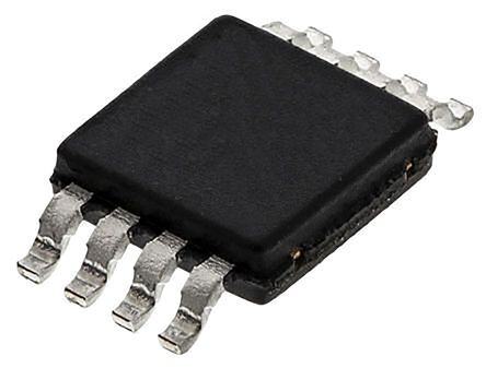
| 产品图片 |
|
| rohs | 符合RoHS无铅 / 符合限制有害物质指令(RoHS)规范要求 |
| 产品系列 | 数据转换器IC,模数转换器 - ADC,Texas Instruments ADS8326IDGKTmicroPOWER™ |
| 数据手册 | |
| 产品型号 | ADS8326IDGKT |
| PCN封装 | |
| 产品培训模块 | http://www.digikey.cn/PTM/IndividualPTM.page?site=cn&lang=zhs&ptm=13240 |
| 产品目录页面 | |
| 产品种类 | 模数转换器 - ADC |
| 位数 | 16 |
| 供应商器件封装 | 8-VSSOP |
| 信噪比 | 91 dB |
| 其它名称 | 296-21947-2 |
| 分辨率 | 16 bit |
| 制造商产品页 | http://www.ti.com/general/docs/suppproductinfo.tsp?distId=10&orderablePartNumber=ADS8326IDGKT |
| 包装 | Digi-Reel® |
| 单位重量 | 26.500 mg |
| 商标 | Texas Instruments |
| 安装类型 | 表面贴装 |
| 安装风格 | SMD/SMT |
| 封装 | Reel |
| 封装/外壳 | 8-TSSOP,8-MSOP(0.118",3.00mm 宽) |
| 封装/箱体 | VSSOP-8 |
| 工作温度 | -40°C ~ 85°C |
| 工作电源电压 | 2.7 V to 5.5 V |
| 工厂包装数量 | 250 |
| 接口类型 | 3-Wire, Serial, SPI |
| 数据接口 | SPI |
| 最大功率耗散 | 15 mW |
| 最大工作温度 | + 85 C |
| 最小工作温度 | - 40 C |
| 标准包装 | 250 |
| 特性 | - |
| 电压参考 | External |
| 电压源 | 单电源 |
| 系列 | ADS8326 |
| 结构 | SAR |
| 视频文件 | http://www.digikey.cn/classic/video.aspx?PlayerID=1364138032001&width=640&height=455&videoID=30090072001 |
| 转换器数 | 1 |
| 转换器数量 | 1 |
| 转换速率 | 250 kS/s |
| 输入数和类型 | 2 个单端,双极1 个差分,双极 |
| 输入类型 | Single-Ended/Differential |
| 通道数量 | 1 Channel |
| 配用 | /product-detail/zh/ADS8326EVM/296-30705-ND/1895872 |
| 采样率(每秒) | 250k |


- 商务部:美国ITC正式对集成电路等产品启动337调查
- 曝三星4nm工艺存在良率问题 高通将骁龙8 Gen1或转产台积电
- 太阳诱电将投资9.5亿元在常州建新厂生产MLCC 预计2023年完工
- 英特尔发布欧洲新工厂建设计划 深化IDM 2.0 战略
- 台积电先进制程称霸业界 有大客户加持明年业绩稳了
- 达到5530亿美元!SIA预计今年全球半导体销售额将创下新高
- 英特尔拟将自动驾驶子公司Mobileye上市 估值或超500亿美元
- 三星加码芯片和SET,合并消费电子和移动部门,撤换高东真等 CEO
- 三星电子宣布重大人事变动 还合并消费电子和移动部门
- 海关总署:前11个月进口集成电路产品价值2.52万亿元 增长14.8%


PDF Datasheet 数据手册内容提取
ADS8326 www.ti.com.................................................................................................................................................. SBAS343C–MAY2007–REVISEDSEPTEMBER2009 16-Bit, High-Speed, 2.7V to 5.5V microPower Sampling ANALOG-TO-DIGITAL CONVERTER CheckforSamples:ADS8326 FEATURES APPLICATIONS 1 • 16BitsNoMissingCodes(Full-SupplyRange, • Battery-OperatedSystems 23 HighorLowGrade) • RemoteDataAcquisition • VeryLowNoise:3LSB • IsolatedDataAcquisition PP • ExcellentLinearity: • SimultaneousSampling,Multichannel ±1LSBtyp, ±1.5LSBmaxINL Systems ±0.6LSBtyp, ±1LSBmaxDNL • IndustrialControls ±1mVmaxOffset • Robotics ±12LSBtypGainError • VibrationAnalysis • microPower: 10mWat5V,250kHz DESCRIPTION 4mWat2.7V,200kHz The ADS8326 is a 16-bit, sampling, analog-to-digital 2mWat2.7V,100kHz (A/D) converter specified for a supply voltage range 0.2mWat2.7V,10kHz from 2.7V to 5.5V. It requires very little power, even • MSOP-8andSON-8Packages when operating at the full data rate. At lower data (SON-8packagesameas3x3QFN) rates, the high speed of the device enables it to spend most of its time in the power-down mode. For • 16-BitUpgradetothe12-BitADS7816and example, the average power dissipation is less than ADS7822 0.2mWata10kHzdatarate. • Pin-CompatiblewiththeADS7816,ADS7822, The ADS8326 offers excellent linearity and very low ADS7826,ADS7827,ADS7829,ADS8320,and noise and distortion. It also features a synchronous ADS8325 serial (SPI/SSI-compatible) interface and a differential • Serial(SPI™/SSI)Interface input. The reference voltage can be set to any level withintherangeof0.1VtoV . DD Low power and small size make the ADS8326 ideal for portable and battery-operated systems. It is also a perfect fit for remote data-acquisition modules, simultaneous multichannel systems, and isolated data acquisition. The ADS8326 is available in either anMSOP-8andanSON-8package. SAR REF ADS8326 D OUT +IN CDAC Serial -IN Interface DCLOCK S/H Amp Comparator CS/SHDN 1 Pleasebeawarethatanimportantnoticeconcerningavailability,standardwarranty,anduseincriticalapplicationsofTexas Instrumentssemiconductorproductsanddisclaimerstheretoappearsattheendofthisdatasheet. SPIisatrademarkofMotorola,Inc. 2 Allothertrademarksarethepropertyoftheirrespectiveowners. 3 PRODUCTIONDATAinformationiscurrentasofpublicationdate. Copyright©2007–2009,TexasInstrumentsIncorporated Products conform to specifications per the terms of the Texas Instruments standard warranty. Production processing does not necessarilyincludetestingofallparameters.
ADS8326 SBAS343C–MAY2007–REVISEDSEPTEMBER2009.................................................................................................................................................. www.ti.com This integrated circuit can be damaged by ESD. Texas Instruments recommends that all integrated circuits be handled with appropriateprecautions.Failuretoobserveproperhandlingandinstallationprocedurescancausedamage. ESDdamagecanrangefromsubtleperformancedegradationtocompletedevicefailure.Precisionintegratedcircuitsmaybemore susceptibletodamagebecauseverysmallparametricchangescouldcausethedevicenottomeetitspublishedspecifications. ORDERINGINFORMATION(1) MAXIMUM NO INTEGRAL MISSING LINEARITY CODES SPECIFIED TRANSPORT ERROR ERROR PACKAGE- PACKAGE TEMPERATURE PACKAGE ORDERING MEDIA, PRODUCT (LSB)(2) (LSB) LEAD DESIGNATOR RANGE MARKING NUMBER QUANTITY TapeandReel, ADS8326IDGKT 250 ADS8326I ±3 16 MSOP-8 DGK –40°Cto+85°C D26 TapeandReel, ADS8326IDGKR 2500 TapeandReel, ADS8326IBDGKT 250 ADS8326IB ±1.5 16 MSOP-8 DGK –40°Cto+85°C D26 TapeandReel, ADS8326IBDGKR 2500 TapeandReel, ADS8326IDRBT 250 ADS8326I ±3 16 SON-8 DRB –40°Cto+85°C D26 TapeandReel, ADS8326IDRBR 2500 TapeandReel, ADS8326IBDRBT 250 ADS8326IB ±1.5 16 SON-8 DRB –40°Cto+85°C D26 TapeandReel, ADS8326IBDRBR 2500 (1) Forthemostcurrentpackageandorderinginformation,seethePackageOptionAddendumlocatedattheendofthisdatasheet,orsee theTIwebsiteatwww.ti.com. (2) MaximumIntegralLinearityErrorspecifiesa5Vpowersupplyandreferencevoltage. ABSOLUTE MAXIMUM RATINGS(1) Overoperatingfree-airtemperaturerange(unlessotherwisenoted). ADS8326 UNIT Supplyvoltage,V toGND –0.3to+7 V DD Analoginputvoltage(2) –0.3toV +0.3 V DD Referenceinputvoltage(2) –0.3toV +0.3 V DD Digitalinputvoltage(2) –0.3toV +0.3 V DD Inputcurrenttoanypinexceptsupply –20to+20 mA Powerdissipation SeeDissipationRatingsTable Operatingvirtualjunctiontemperaturerange,T –40to+150 °C J Operatingfree-airtemperaturerange,T –40to+85 °C A Storagetemperaturerange,T –65to+150 °C STG LeadTemperature1.6mm(1/16inch)fromcasefor10sec +260 °C (1) StressesbeyondthoselistedunderAbsoluteMaximumRatingsmaycausepermanentdamagetothedevice.Thesearestressratings only,andfunctionaloperationofthedeviceattheseoranyotherconditionsbeyondthoseindicatedunderRecommendedOperating Conditionsisnotimplied.Exposuretoabsolute-maximumratedconditionsforextendedperiodsmayaffectdevicereliability. (2) Allvoltagevaluesarewithrespecttogroundterminal. 2 SubmitDocumentationFeedback Copyright©2007–2009,TexasInstrumentsIncorporated ProductFolderLink(s):ADS8326
ADS8326 www.ti.com.................................................................................................................................................. SBAS343C–MAY2007–REVISEDSEPTEMBER2009 DISSIPATION RATINGS DERATING FACTORABOVE T ≤+25°C T =+70°C T =+85°C A A A PACKAGE R R T =+25°C POWERRATING POWERRATING POWERRATING θJC θJA A DGK +39.1°C/W +206.3°C/W 4.847mW/°C 606mW 388mW 315mW DRB +5°C/W +45.8°C/W 3.7mW/°C 370mW 204mW 148mW RECOMMENDED OPERATING CONDITIONS MIN TYP MAX UNIT Supplyvoltage,GNDtoV Low-voltagelevels 2.7 3.6 V DD Supplyvoltage,GNDtoV 5Vlogiclevels 4.5 5.0 5.5 V DD Referenceinputvoltage 0.1 V V DD –INtoGND –0.3 0 0.5 V Analoginputvoltage +INtoGND –0.3 V +0.2 V DD +IN–(–IN) 0 V V REF Operatingjunctiontemperature,T –40 +125 °C J ELECTRICAL CHARACTERISTICS: V = +5V DD At–40°Cto+85°C,V =+5V,–IN=GND,f =250kHz,andf =24×f ,unlessotherwisenoted. REF SAMPLE DCLOCK SAMPLE ADS8326I ADS8326IB PARAMETER TESTCONDITIONS MIN TYP MAX MIN TYP MAX UNIT ANALOGINPUT Full-scalerange FSR +IN–(–IN) 0 VREF 0 VREF V Operatingcommon-modesignal –0.3 0.5 –0.3 0.5 V –IN=GND,off 5 5 GΩ Inputresistance RON –IN=GND,on 50 100 50 100 Ω Inputcapacitance –IN=GND,duringsampling 48 48 pF Inputleakagecurrent –IN=GND ±50 ±50 nA Differentialinputcapacitance +INto–IN,duringsampling 20 20 pF FSsinewave,SINAD= Full-powerbandwidth FSBW 500 500 kHz –60dB DCACCURACY Resolution 16 16 Bits Nomissingcodes NMC 16 16 Bits Integrallinearityerror INL –3 ±2 +3 –1.5 ±1 +1.5 LSB Differentiallinearityerror DNL –1 ±0.5 +2 –1 ±0.4 +1 LSB Offseterror VOS –1.5 ±0.75 +1.5 –1 ±0.5 +1 mV Offseterrordrift TCVOS ±0.2 ±0.2 ppm/°C Gainerror GERR –24 +24 –12 +12 LSB Gainerrordrift TCGERR ±0.3 ±0.3 ppm/°C Noise 30 30 μVRMS Power-supplyrejection 4.75V≤VDD≤5.25V 0.5 0.5 LSB SAMPLINGDYNAMICS Conversiontime (16DCLOCKs) tCONV 24kHz≤fDCLOCK≤6MHz 2.667 666.7 2.667 666.7 μs Acquisitiontime (4.5DCLOCKs) tAQ fDCLOCK=6MHz 0.75 0.75 μs Throughputrate 250 250 kSPS (22DCLOCKs) Clockfrequency fDCLOCK 0.024 6 0.024 6 MHz Copyright©2007–2009,TexasInstrumentsIncorporated SubmitDocumentationFeedback 3 ProductFolderLink(s):ADS8326
ADS8326 SBAS343C–MAY2007–REVISEDSEPTEMBER2009.................................................................................................................................................. www.ti.com ELECTRICAL CHARACTERISTICS: V = +5V (continued) DD At–40°Cto+85°C,V =+5V,–IN=GND,f =250kHz,andf =24×f ,unlessotherwisenoted. REF SAMPLE DCLOCK SAMPLE ADS8326I ADS8326IB PARAMETER TESTCONDITIONS MIN TYP MAX MIN TYP MAX UNIT ACACCURACY 5VPPsinewaveat2kHz –98 –99 dB Totalharmonicdistortion THD 5VPPsinewaveat10kHz –90 –91 dB Spurious-freedynamic 5VPPsinewaveat2kHz 102 103 dB SFDR range 5VPPsinewaveat10kHz 94 95 dB 5VPPsinewaveat2kHz 91 91.5 dB Signal-to-noiseratio SNR 5VPPsinewaveat10kHz 91 91.5 dB 5VPPsinewaveat2kHz 90 91 dB Signal-to-noise+distortion SINAD 5VPPsinewaveat10kHz 87.5 88 dB 5VPPsinewaveat2kHz 14.69 14.86 Bits Effectivenumberofbits ENOB 5VPPsinewaveat10kHz 14.28 14.35 Bits VOLTAGEREFERENCEINPUT Referencevoltage 0.1 VDD 0.1 VDD V CS=GND,fSAMPLE=0Hz 5 5 GΩ Referenceinputresistance CS=VDD 5 5 GΩ Referenceinputcapacitance 24 24 pF fS=250kHz 170 220 170 220 μA fS=200kHz 140 180 140 180 μA Referenceinputcurrent fS=100kHz 70 90 70 90 μA fS=10kHz 11 14 11 14 μA CS=VDD 0.1 0.1 μA DIGITALINPUTS(1) Logicfamily CMOS CMOS High-levelinputvoltage VIH 0.7×VDD VDD+0.3 0.7×VDD VDD+0.3 V Low-levelinputvoltage VIL –0.3 0.3×VDD –0.3 0.3×VDD V Inputcurrent IIN VI=VDDorGND –50 +50 –50 +50 nA Inputcapacitance CI 5 5 pF DIGITALOUTPUTS(1) Logicfamily CMOS CMOS High-leveloutputvoltage VOH VDD=4.5V,IOH=–100μA 4.44 4.44 V Low-leveloutputvoltage VOL VDD=4.5V,IOL=100μA 0.5 0.5 V High-impedancestate outputcurrent IOZ CS=VDD,VI=VDDorGND –50 +50 –50 +50 nA Outputcapacitance CO 5 5 pF Loadcapacitance CL 30 30 pF Straight Straight Dataformat binary binary (1) Appliesfor5.0Vnominalsupply:V (min)=4.5VandV (max)=5.5V. DD DD 4 SubmitDocumentationFeedback Copyright©2007–2009,TexasInstrumentsIncorporated ProductFolderLink(s):ADS8326
ADS8326 www.ti.com.................................................................................................................................................. SBAS343C–MAY2007–REVISEDSEPTEMBER2009 ELECTRICAL CHARACTERISTICS: V = +2.7V DD At–40°Cto+85°C,V =+2.5V,–IN=GND,f =200kHz,andf =24×f ,unlessotherwisenoted. REF SAMPLE DCLOCK SAMPLE ADS8326I ADS8326IB PARAMETER TESTCONDITIONS MIN TYP MAX MIN TYP MAX UNIT ANALOGINPUT Full-scalerange FSR +IN–(–IN) 0 VREF 0 VREF V Operatingcommon-modesignal –0.3 0.5 –0.3 0.5 V –IN=GND,off 5 5 GΩ Inputresistance RON –IN=GND,on 100 150 100 150 Ω Inputcapacitance –IN=GND,duringsampling 48 48 pF Inputleakagecurrent –IN=GND ±50 ±50 nA Differentialinputcapacitance +INto–IN,duringsampling 20 20 pF FSsinewave,SINAD= Full-powerbandwidth FSBW 60 60 kHz –60dB DCACCURACY Resolution 16 16 Bits Nomissingcodes NMC 16 16 Bits Integrallinearityerror INL –3 ±2 +3 –2.5 ±1 +2.5 LSB Differentiallinearityerror DNL –1 ±0.5 +2 –1 ±0.4 +1 LSB Offseterror VOS –1.5 ±0.75 +1.5 –1 ±0.5 +1 mV Offseterrordrift TCVOS ±0.2 ±0.2 ppm/°C Gainerror GERR ±33 ±16 LSB Gainerrordrift TCGERR ±0.3 ±0.3 ppm/°C Noise 30 30 μVRMS Power-supplyrejection 2.7V≤VDD≤3.6V 0.5 0.5 LSB SAMPLINGDYNAMICS Conversiontime (16DCLOCKs) tCONV 24kHz≤fDCLOCK≤4.8MHz 3.333 666.7 3.333 666.7 μs Acquisitiontime (4.5DCLOCKs) tAQ fDCLOCK=4.8MHz 0.9375 0.9375 μs Throughputrate 200 200 kSPS (22DCLOCKs) Clockfrequency fDCLOCK 0.024 4.8 0.024 4.8 MHz ACACCURACY 2.5VPPsinewaveat2kHz –88 –88.5 dB Totalharmonicdistortion THD 2.5VPPsinewaveat10kHz –75 –75.5 dB Spurious-freedynamic 2.5VPPsinewaveat2kHz 91 91.5 dB SFDR range 2.5VPPsinewaveat10kHz 77.5 78 dB 2.5VPPsinewaveat2kHz 86.5 87 dB Signal-to-noiseratio SNR 2.5VPPsinewaveat10kHz 86 86.5 dB 2.5VPPsinewaveat2kHz 85 85.5 dB Signal-to-noise+distortion SINAD 2.5VPPsinewaveat10kHz 74.5 75 dB 2.5VPPsinewaveat2kHz 13.86 13.94 Bits Effectivenumberofbits ENOB 2.5VPPsinewaveat10kHz 12.12 12.20 Bits VOLTAGEREFERENCEINPUT Referencevoltage 0.1 VDD 0.1 VDD V CS=GND,fSAMPLE=0Hz 5 5 GΩ Referenceinputresistance CS=VDD 5 5 GΩ Referenceinputcapacitance 24 24 pF fS=200kHz 70 90 70 90 μA fS=100kHz 25 33 25 33 μA Referenceinputcurrent fS=10kHz 5 7 5 7 μA CS=VDD 0.1 0.1 μA Copyright©2007–2009,TexasInstrumentsIncorporated SubmitDocumentationFeedback 5 ProductFolderLink(s):ADS8326
ADS8326 SBAS343C–MAY2007–REVISEDSEPTEMBER2009.................................................................................................................................................. www.ti.com ELECTRICAL CHARACTERISTICS: V = +2.7V (continued) DD At–40°Cto+85°C,V =+2.5V,–IN=GND,f =200kHz,andf =24×f ,unlessotherwisenoted. REF SAMPLE DCLOCK SAMPLE ADS8326I ADS8326IB PARAMETER TESTCONDITIONS MIN TYP MAX MIN TYP MAX UNIT DIGITALINPUTS(1) Logicfamily LVCMOS LVCMOS High-levelinputvoltage VIH VDD=3.6V 2 VDD+0.3 2 VDD+0.3 V Low-levelinputvoltage VIL VDD=2.7V –0.3 0.8 –0.3 0.8 V Inputcurrent IIN VI=VDDorGND –50 +50 –50 +50 nA Inputcapacitance CI 5 5 pF DIGITALOUTPUTS(1) Logicfamily LVCMOS LVCMOS High-leveloutputvoltage VOH VDD=2.7V,IOH=–100μA VDD–0.2 VDD–0.2 V Low-leveloutputvoltage VOL VDD=2.7V,IOL=100μA 0.2 0.2 V High-impedancestate outputcurrent IOZ CS=VDD,VI=VDDorGND –50 +50 –50 +50 nA Outputcapacitance CO 5 5 pF Loadcapacitance CL 30 30 pF Straight Straight Dataformat binary binary (1) Appliesfor3.0Vnominalsupply:V (min)=2.7VandV (max)=3.6V. DD DD ELECTRICAL CHARACTERISTICS At–40°Cto+85°C,–IN=GND,andf =24×f ,unlessotherwisenoted. DCLOCK SAMPLE ADS8326I ADS8326IB PARAMETER TESTCONDITIONS MIN TYP MAX MIN TYP MAX UNIT ANALOGINPUT Low-voltagelevels 2.7 3.6 2.7 3.6 V Powersupply VDD 5Vlogiclevels 4.5 5.5 4.5 5.5 V VDD=2.7V,fS=10kHz, 0.065 0.085 0.065 0.085 mA fDCLOCK=4.8MHz VDD=2.7V,fS=100kHz, 0.69 1.0 0.69 1.0 mA fDCLOCK=4.8MHz Operatingsupplycurrent IDD VfDDCDLO=CK2.=7V4,.8fSM=Hz200kHz, 1.38 2.0 1.38 2.0 mA VDD=5V,fS=200kHz, 1.9 2.7 1.9 2.7 mA fDCLOCK=6MHz VDD=5V,fS=250kHz, 2.0 3.0 2.0 3.0 mA fDCLOCK=6MHz VDD=2.7V 0.1 0.1 μA Power-downsupplycurrent IDD VDD=5V 0.2 0.2 μA VDD=2.7V,fS=10kHz, 0.18 0.23 0.18 0.23 mW fDCLOCK=4.8MHz VDD=2.7V,fS=100kHz, 1.86 2.7 1.86 2.7 mW fDCLOCK=4.8MHz Powerdissipation VDD=2.7V,fS=200kHz, 3.73 5.4 3.73 5.4 mW fDCLOCK=4.8MHz VDD=5V,fS=200kHz, 9.5 13.5 9.5 13.5 mW fDCLOCK=6MHz VDD=5V,fS=250kHz, 10 15 10 15 mW fDCLOCK=6MHz VDD=2.7V,CS=VDD 0.3 0.3 μW Powerdissipationinpower-down VDD=5V,CS=VDD 0.6 0.6 μW 6 SubmitDocumentationFeedback Copyright©2007–2009,TexasInstrumentsIncorporated ProductFolderLink(s):ADS8326
ADS8326 www.ti.com.................................................................................................................................................. SBAS343C–MAY2007–REVISEDSEPTEMBER2009 PIN CONFIGURATION DGKPACKAGE MSOP-8 (TOPVIEW) REF 1 8 V DD +IN 2 7 DCLOCK ADS8326 -IN 3 6 D OUT GND 4 5 CS/SHDN DRBPACKAGE SON-8 (TOPVIEW) REF 1 8 V DD +IN 2 7 DCLOCK ADS8326 -IN 3 6 D OUT GND 4 (Thermal Pad) 5 CS/SHDN (1) The thermal pad is internally connected to the substrate. This pad can be connected to the analog ground or left floating.Keepthethermalpadseparatefromthedigitalground,ifpossible. PINASSIGNMENTS PIN I/O DESCRIPTION NAME NO. REF 1 Analoginput Referenceinput +IN 2 Analoginput Noninvertinginput –IN 3 Analoginput Invertinganaloginput GND 4 Power-supplyconnection Ground CS/SHDN 5 Digitalinput Chipselectwhenlow;Shutdownmodewhenhigh. D 6 Digitaloutput Serialoutputdataword OUT DCLOCK 7 Digitalinput Dataclocksynchronizestheserialdatatransferanddeterminesconversionspeed. V 8 Power-supplyconnection Powersupply DD Equivalent Input Circuit (V = 5.0V) DD V V V DD DD DD R C R ON (SAMPLE) ON 50W 48pF 50W 24pF ANALOG IN REF I/O GND GND GND Diode Turn-On Voltage: 0.35V Equivalent Reference Input Circuit Equivalent Digital Input/Output Circuit Equivalent Analog Input Circuit Copyright©2007–2009,TexasInstrumentsIncorporated SubmitDocumentationFeedback 7 ProductFolderLink(s):ADS8326
ADS8326 SBAS343C–MAY2007–REVISEDSEPTEMBER2009.................................................................................................................................................. www.ti.com TIMING INFORMATION t CYC CS/SHDN Power Down Sample Conversion t SUCS DCLOCK t CSD Use positive clock edge for data transfer DOUT Hi-Z 0 B15 B14 B13 B12 B11 B10 B9 B8 B7 B6 B5 B4 B3 B2 B1 B0(1) Hi-Z (MSB) (LSB) t t SMPL CONV NOTE: (1) A minimum of 22 clock cycles are required for 16-bit conversion; 24 clock cycles are shown. IfCSremains low at the end of conversion, a new data stream is shifted out with LSB-first data followed by zeroes indefinitely. t CYC CS/SHDN tSUCS Power Down DCLOCK t CSD DOUT Hi-Z 0 B15 B14 B6 B5 B4 B3 B2 B1 B0 B1 B2 B3 B4 B5 B0 B11B12 B13 B14 B1(52) Hi-Z (MSB) (LSB) (MSB) t t SMPL CONV NOTE: (2) After completing the data transfer, if further clocks are applied withCSlow, the A/D converter will output zeroes indefinitely. 1.4V 3kW 90% D OUT DOUT Test Point 10% t t 100pF r f C LOAD Voltage Waveforms for D Rise and Fall Times, t, t OUT r f Load Circuit for t , t, and t dDO r f Test Point DCLOCK V DD 3kW tdisWaveform 2, ten tdDO DOUT D 100pF tdisWaveform 1 OUT C LOAD t hDO Load Circuit for t and t dis en Voltage Waveforms for D Delay Times, t OUT dDO 90% CS/SHDN CS/SHDN DOUT 90% DCLOCK 1 4 5 Waveform 1(3) t dis DOUT 10% DOUT B15 Waveform 2(4) t en Voltage Waveforms for t dis Voltage Waveforms for t en NOTES:(3) Waveform 1 is for an output with internal conditions such that the output is high unless disabled by the output control. (4) Waveform 2 is for an output with internal conditions such that the output is low unless disabled by the output control. Figure1. TimingDiagramsandTestCircuitsfortheParametersinTable1 8 SubmitDocumentationFeedback Copyright©2007–2009,TexasInstrumentsIncorporated ProductFolderLink(s):ADS8326
ADS8326 www.ti.com.................................................................................................................................................. SBAS343C–MAY2007–REVISEDSEPTEMBER2009 TIMING INFORMATION (continued) Table1.TimingCharacteristics SYMBOL DESCRIPTION MIN TYP MAX UNIT t Analoginputsampletime 4.5 5.0 DCLOCKs SMPL t Conversiontime 16 DCLOCKs CONV t Completecycletime 22 DCLOCKs CYC t CSfallingtoDCLOCKlow 0 ns CSD t CSfallingtoDCLOCKrising 20 ns SUCS t DCLOCKfallingtocurrentD notvalid 5 15 ns HDO OUT t CSrisingtoD tri-state 70 100 ns DIS OUT t DCLOCKfallingtoD enabled 20 50 ns EN OUT t D falltime 5 25 ns F OUT t D risetime 7 25 ns R OUT Copyright©2007–2009,TexasInstrumentsIncorporated SubmitDocumentationFeedback 9 ProductFolderLink(s):ADS8326
ADS8326 SBAS343C–MAY2007–REVISEDSEPTEMBER2009.................................................................................................................................................. www.ti.com TYPICAL CHARACTERISTICS: V = +5V DD AtT =+25°C,V =+5V,V =+5V.f =250kHz,f =24×f ,unlessotherwisenoted. A DD REF SAMPLE CLK SAMPLE INTEGRALLINEARITYERROR DIFFERENTIALLINEARITYERROR vs vs CODE CODE 3 3 2 2 1 1 B) B) S S E (L 0 E (L 0 IL DL -1 -1 -2 -2 -3 -3 0000h 4000h 8000h C000h FFFFh 0000h 4000h 8000h C000h FFFFh Output Code Output Code Figure2. Figure3. CHANGEINOFFSET CHANGEINGAIN vs vs TEMPERATURE TEMPERATURE 0.50 0.50 0.25 0.25 B) B) S S L 0 L C ( C ( 0 °5 °5 +2 -0.25 +2 om om -0.25 a fr -0.50 a fr elt elt D -0.75 D -0.50 -1.00 -0.75 -50 -25 0 25 50 75 100 -50 -25 0 25 50 75 100 Temperature (°C) Temperature (°C) Figure4. Figure5. 10 SubmitDocumentationFeedback Copyright©2007–2009,TexasInstrumentsIncorporated ProductFolderLink(s):ADS8326
ADS8326 www.ti.com.................................................................................................................................................. SBAS343C–MAY2007–REVISEDSEPTEMBER2009 TYPICAL CHARACTERISTICS: V = +5V (continued) DD AtT =+25°C,V =+5V,V =+5V.f =250kHz,f =24×f ,unlessotherwisenoted. A DD REF SAMPLE CLK SAMPLE CHANGEINOFFSET CHANGEINGAIN vs vs COMMON-MODEVOLTAGE COMMON-MODEVOLTAGE 30 30 B) 25 B) 25 S S L L V ( 20 V ( 20 0 0 = 15 = 15 M M C C V V o 10 o 10 e t e t ativ 5 ativ 5 el el R 0 R 0 a a Delt -5 Delt -5 -10 -10 -0.5 -0.4 -0.3-0.2 -0.1 0 0.1 0.2 0.3 0.4 0.5 0.6 -0.5 -0.4 -0.3-0.2 -0.1 0 0.1 0.2 0.3 0.4 0.5 0.6 V (V) V (V) CM CM Figure6. Figure7. FREQUENCYSPECTRUM FREQUENCYSPECTRUM (8192pointFFT,f =1.9836kHz,–0.2dB) (8192pointFFT,f =9.9792kHz,–0.2dB) IN IN 0 0 -20 -20 -40 -40 dB) -60 dB) -60 e ( e ( ud -80 ud -80 mplit -100 mplit -100 A A -120 -120 -140 -140 -160 -160 0 25 50 75 100 125 0 25 50 75 100 125 Frequency (kHz) Frequency (kHz) Figure8. Figure9. Copyright©2007–2009,TexasInstrumentsIncorporated SubmitDocumentationFeedback 11 ProductFolderLink(s):ADS8326
ADS8326 SBAS343C–MAY2007–REVISEDSEPTEMBER2009.................................................................................................................................................. www.ti.com TYPICAL CHARACTERISTICS: V = +5V (continued) DD AtT =+25°C,V =+5V,V =+5V.f =250kHz,f =24×f ,unlessotherwisenoted. A DD REF SAMPLE CLK SAMPLE SIGNAL-TO-NOISEAND SPURIOUS-FREEDYNAMICRANGEAND SIGNAL-TO-NOISE+DISTORTION TOTALHARMONICDISTORTION vs vs INPUTFREQUENCY INPUTFREQUENCY 100 105 -105 SNR 95 100 -100 SFDR B) 90 95 -95 d and SINAD ( 8850 SINAD SFDR (dB) 988050 THD(1) ---988050 THD (dB) R SN 75 75 -75 70 70 -70 NOTE: (1) First nine harmonics of the input frequency. 65 65 -65 1 10 100 200 1 10 100 200 Frequency (kHz) Frequency (kHz) Figure10. Figure11. EFFECTIVENUMBEROFBITS CHANGEINSIGNAL-TO-NOISE+DISTORTION vs vs INPUTFREQUENCY TEMPERATURE 16.0 0.25 f = 1.98364kHz,-0.2dB 0.20 IN 15.0 0.15 B) OB (Bits) 1143..00 °m +25C (d 00..10050 EN 12.0 a fro -0.05 elt D -0.10 11.0 -0.15 10.0 -0.20 1 10 100 200 -50 -25 0 25 50 75 100 Frequency (kHz) Temperature (°C) Figure12. Figure13. 12 SubmitDocumentationFeedback Copyright©2007–2009,TexasInstrumentsIncorporated ProductFolderLink(s):ADS8326
ADS8326 www.ti.com.................................................................................................................................................. SBAS343C–MAY2007–REVISEDSEPTEMBER2009 TYPICAL CHARACTERISTICS: V = +5V (continued) DD AtT =+25°C,V =+5V,V =+5V.f =250kHz,f =24×f ,unlessotherwisenoted. A DD REF SAMPLE CLK SAMPLE SIGNAL-TO-NOISE+DISTORTION PEAK-TO-PEAKNOISEFORADCINPUT vs vs INPUTLEVEL REFERENCEVOLTAGE 100 200 f = 1.98364kHz,-0.2dB 90 IN 100 80 B) S L NAD (dB) 765000 eak Noise ( 10 SI 40 k-to-P a 30 e P 20 10 1 -80 -70 -60 -50 -40 -30 -20 -10 0 0.1 1 5 Input Level (dB) Reference Voltage (V) Figure14. Figure15. SUPPLYCURRENT SUPPLYCURRENT vs vs TEMPERATURE SAMPLINGRATE 1.84 10 1.83 1 A) A) m m nt ( 1.82 nt ( e e urr urr 0.1 C C y 1.81 y pl pl p p u u S S 0.01 1.80 1.79 0.001 -50 -25 0 25 50 75 100 1 10 100 250 Temperature (°C) Sampling Rate (kHz) Figure16. Figure17. Copyright©2007–2009,TexasInstrumentsIncorporated SubmitDocumentationFeedback 13 ProductFolderLink(s):ADS8326
ADS8326 SBAS343C–MAY2007–REVISEDSEPTEMBER2009.................................................................................................................................................. www.ti.com TYPICAL CHARACTERISTICS: V = +5V (continued) DD AtT =+25°C,V =+5V,V =+5V.f =250kHz,f =24×f ,unlessotherwisenoted. A DD REF SAMPLE CLK SAMPLE REFERENCECURRENT POWER-DOWNCURRENT vs vs SAMPLINGRATE TEMPERATURE 1000 30 28 A) 100 nA) mnt ( ent ( 26 urre Curr e C 10 wn 24 Referenc 1 ower-Do 22 P 20 0.1 18 1 10 100 250 -50 -25 0 25 50 75 100 Sampling Rate (kHz) Temperature (°C) Figure18. Figure19. OUTPUTCODEHISTOGRAMFORADCINPUT (8192Conversions) 6990 e c n e urr c c O 592 610 0 0 0 0 7FFC 7FFD 7FFE 7FFF 8000 8001 8002 Code Figure20. 14 SubmitDocumentationFeedback Copyright©2007–2009,TexasInstrumentsIncorporated ProductFolderLink(s):ADS8326
ADS8326 www.ti.com.................................................................................................................................................. SBAS343C–MAY2007–REVISEDSEPTEMBER2009 TYPICAL CHARACTERISTICS: V = +2.7V DD AtT =+25°C,V =+2.7V,V =+2.5V.f =200kHz,f =24×f ,unlessotherwisenoted. A DD REF SAMPLE CLK SAMPLE INTEGRALLINEARITYERROR DIFFERENTIALLINEARITYERROR vs vs CODE CODE 3 3 2 2 1 1 B) B) S S E (L 0 E (L 0 L L I D -1 -1 -2 -2 -3 -3 0000h 4000h 8000h C000h FFFFh 0000h 4000h 8000h C000h FFFFh Output Code Output Code Figure21. Figure22. CHANGEINOFFSET CHANGEINGAIN vs vs TEMPERATURE TEMPERATURE 0.50 0.50 0.25 0.25 B) B) S S L 0 L 0 C ( C ( °5 °5 +2 -0.25 +2 -0.25 m m o o a fr -0.50 a fr -0.50 elt elt D D -0.75 -0.75 -1.00 -1.00 -50 -25 0 25 50 75 100 -50 -25 0 25 50 75 100 Temperature (°C) Temperature (°C) Figure23. Figure24. Copyright©2007–2009,TexasInstrumentsIncorporated SubmitDocumentationFeedback 15 ProductFolderLink(s):ADS8326
ADS8326 SBAS343C–MAY2007–REVISEDSEPTEMBER2009.................................................................................................................................................. www.ti.com TYPICAL CHARACTERISTICS: V = +2.7V (continued) DD AtT =+25°C,V =+2.7V,V =+2.5V.f =200kHz,f =24×f ,unlessotherwisenoted. A DD REF SAMPLE CLK SAMPLE CHANGEINOFFSET CHANGEINGAIN vs vs COMMON-MODEVOLTAGE COMMON-MODEVOLTAGE 30 30 B) 25 B) 25 S S L L V ( 20 V ( 20 0 0 = 15 = 15 M M VC VC o 10 o 10 e t e t ativ 5 ativ 5 el el R 0 R 0 a a Delt -5 Delt -5 -10 -10 -0.5 -0.4 -0.3 -0.2 -0.1 0 0.1 0.2 0.3 0.4 0.5 0.6 -0.5 -0.4 -0.3 -0.2 -0.1 0 0.1 0.2 0.3 0.4 0.5 0.6 V (V) V (V) CM CM Figure25. Figure26. FREQUENCYSPECTRUM FREQUENCYSPECTRUM (8192pointFFT,f =1.9775kHz,–0.2dB) (8192pointFFT,f =9.9854kHz,–0.2dB) IN IN 0 0 -20 -20 -40 -40 dB) -60 dB) -60 e ( e ( ud -80 ud -80 mplit -100 mplit -100 A A -120 -120 -140 -140 -160 -160 0 10 20 30 40 50 60 70 80 90 100 0 10 20 30 40 50 60 70 80 90 100 Frequency (kHz) Frequency (kHz) Figure27. Figure28. 16 SubmitDocumentationFeedback Copyright©2007–2009,TexasInstrumentsIncorporated ProductFolderLink(s):ADS8326
ADS8326 www.ti.com.................................................................................................................................................. SBAS343C–MAY2007–REVISEDSEPTEMBER2009 TYPICAL CHARACTERISTICS: V = +2.7V (continued) DD AtT =+25°C,V =+2.7V,V =+2.5V.f =200kHz,f =24×f ,unlessotherwisenoted. A DD REF SAMPLE CLK SAMPLE SIGNAL-TO-NOISEAND SPURIOUS-FREEDYNAMICRANGEAND SIGNAL-TO-NOISE+DISTORTION TOTALHARMONICDISTORTION vs vs INPUTFREQUENCY INPUTFREQUENCY 95 100 -100 90 SNR 95 -95 90 -90 85 R and SINAD (dB) 87760055 SINAD SFDR (dB) 887766505050 TSHFDDR(1) ------887766505050 THD (dB) N 60 S 55 -55 55 50 -50 50 45 -45 NOTE: (1) First nine harmonics of the input frequency. 55 40 -40 1 10 100 200 1 10 100 200 Frequency (kHz) Frequency (kHz) Figure29. Figure30. EFFECTIVENUMBEROFBITS CHANGEINSIGNAL-TO-NOISE+DISTORTION vs vs INPUTFREQUENCY TEMPERATURE 15 0.4 f = 1.97754kHz,-0.2dB IN 14 0.2 13 B) OB (Bits) 1121 °m +25C (d -0.02 EN 10 a fro -0.4 9 Delt -0.6 8 7 -0.8 1 10 100 200 -50 -25 0 25 50 75 100 Frequency (kHz) Temperature (°C) Figure31. Figure32. Copyright©2007–2009,TexasInstrumentsIncorporated SubmitDocumentationFeedback 17 ProductFolderLink(s):ADS8326
ADS8326 SBAS343C–MAY2007–REVISEDSEPTEMBER2009.................................................................................................................................................. www.ti.com TYPICAL CHARACTERISTICS: V = +2.7V (continued) DD AtT =+25°C,V =+2.7V,V =+2.5V.f =200kHz,f =24×f ,unlessotherwisenoted. A DD REF SAMPLE CLK SAMPLE SIGNAL-TO-NOISE+DISTORTION SUPPLYCURRENT vs vs INPUTLEVEL TEMPERATURE 100 1.38 f = 1.97754kHz,-0.2dB IN 90 1.37 80 1.36 A) 70 m NAD (dB) 6500 Current ( 11..3354 SI 40 pply 1.33 u S 1.32 30 20 1.31 10 1.30 -80 -70 -60 -50 -40 -30 -20 -10 0 -50 -25 0 25 50 75 100 Input Level (dB) Temperature (°C) Figure33. Figure34. SUPPLYCURRENT REFERENCECURRENT vs vs SAMPLINGRATE SAMPLINGRATE 10 1000 1 A) mA) 100 Current (m 0.1 e Current ( 10 ply 0.01 enc Sup efer 1 R 0.001 0.0001 0.1 1 10 100 200 1 10 100 200 Sampling Rate (kHz) Sampling Rate (kHz) Figure35. Figure36. OUTPUTCODEHISTOGRAMFORADCINPUT (8192Conversions) 4791 e c n e urr c c O 1665 1643 0 53 40 0 7FFC 7FFD 7FFE 7FFF 8000 8001 8002 Code Figure37. 18 SubmitDocumentationFeedback Copyright©2007–2009,TexasInstrumentsIncorporated ProductFolderLink(s):ADS8326
ADS8326 www.ti.com.................................................................................................................................................. SBAS343C–MAY2007–REVISEDSEPTEMBER2009 THEORY OF OPERATION The ADS8326 is a classic Successive Approximation The external clock can vary between 24kHz (1kHz Register (SAR) Analog-to-Digital (A/D) converter. The throughput) and 6.0MHz (250kHz throughput). The architecture is based on capacitive redistribution that duty cycle of the clock is essentially unimportant, as inherently includes a sample-and-hold function. The long as the minimum high and low times are at least converter is fabricated on a 0.6μ CMOS process. The 200ns (V = 4.75V or greater). The minimum clock DD architecture and process allow the ADS8326 to frequency is set by the leakage on the internal acquire and convert an analog signal at up to capacitorstotheADS8326. 250,000 conversions per second while consuming The analog input is provided to two input pins: +IN lessthan10mWfromV . DD and –IN. When a conversion is initiated, the Differential linearity for the ADS8326 is differential input on these pins is sampled on the factory-adjusted via a package-level trim procedure. internal capacitor array. While a conversion is in Thestateofthetrimelementsisstoredinnon-volatile progress, both inputs are disconnected from any memory and is continuously updated after each internalfunction. acquisition cycle, just prior to the start of the The digital result of the conversion is clocked out by successive approximation operation. This process the DCLOCK input and is provided serially (most ensures that one complete conversion cycle always significantbitfirst)ontheD pin. returns the part to its factory-adjusted state in the OUT eventofapowerinterruption. The digital data that is provided on the D pin is for OUT the conversion currently in progress–there is no The ADS8326 requires an external reference, an pipeline delay. It is possible to continue to clock the external clock, and a single power source (V ). The DD ADS8326 after the conversion is complete and to external reference can be any voltage between 0.1V obtain the serial data least significant bit first. See the and V . The value of the reference voltage directly DD TimingInformationsectionformoreinformation. sets the range of the analog input. The reference input current depends on the conversion rate of the ADS8326. Copyright©2007–2009,TexasInstrumentsIncorporated SubmitDocumentationFeedback 19 ProductFolderLink(s):ADS8326
ADS8326 SBAS343C–MAY2007–REVISEDSEPTEMBER2009.................................................................................................................................................. www.ti.com ANALOG INPUT The analog input of ADS8326 is differential. The +IN 0V to +V REF ADS8326 and –IN input pins allow for a differential input signal. Peak-to-Peak The amplitude of the input is the difference between the +IN and –IN input, or (+IN) – (–IN). Unlike some Common-Mode Voltage converters of this type, the –IN input is not resampled later in the conversion cycle. When the converter goes into Hold mode or conversion, the voltage Figure38. MethodsofDrivingtheADS8326 difference between +IN and –IN is captured on the internalcapacitorarray. The range of the –IN input is limited to –0.3V to +0.5V. As a result of this limitation, the differential 1 itnopbuottchouinldpubtesuinsetdhetosrpeejecciftiesdignraanlsgeth.aTthaures,ctohmem–oINn nge (V) 0.5 VDD= 5V input is best used to sense a remote signal ground Ra that may move slightly with respect to the local ge a 0 groundpotential. olt n V -0.3 Thegeneralmethodfordrivingtheanaloginputofthe mo ADS8326 is shown in Figure 38 and Figure 40. The m o C –IN input is held at the common-mode voltage. The -1 +IN input swings from –IN (or common-mode voltage) 2 2.5 3 4 4.8 5 6 to –IN + V (or common-mode voltage + V ), REF REF VREF(V) and the peak-to-peak amplitude is +V . The value REF of V determines the range over which the REF Figure39. +INAnalogInput:Common-Mode common-mode voltage may vary, as shown in VoltageRangevsV Figure 39. Figure 6 and Figure 7 (+5V), and REF Figure 25 and Figure 26 (+2.7V) illustrate the typical change in gain and offset as a function of the common-modevoltageappliedtothe–INpin. Common-Mode Voltage+ V +IN REF +V REF Common-ModeVoltage t -IN = Common-Mode Voltage NOTE: The maximum differential voltage between +IN and –IN of the ADS8326 is V . See Figure 39 for a further REF explanationofthecommon-modevoltagerangefordifferentialinputs. Figure40. DifferentialInputModeoftheADS8326 20 SubmitDocumentationFeedback Copyright©2007–2009,TexasInstrumentsIncorporated ProductFolderLink(s):ADS8326
ADS8326 www.ti.com.................................................................................................................................................. SBAS343C–MAY2007–REVISEDSEPTEMBER2009 The input current required by the analog inputs Single-Ended depends on a number of factors: sample rate, input voltage, source impedance, and power-down mode. Essentially, the current into the ADS8326 charges the 10W +IN 50W 48pF internal capacitor array during the sample period. OPA365 After this capacitance has been fully charged, there is 1000pF no further input current. The source of the analog ADS8326 input voltage must be able to charge the input -IN 50W 48pF capacitance (48pF) to a 16-bit settling level within 4.5 clock cycles (0.750μs). When the converter goes into Hold mode, or while it is in Power-Down mode, the inputimpedanceisgreaterthan1GΩ. Differential Care must be taken regarding the absolute analog icnopnuvtertveorl,tathgee.–INToinpmutasinhtoauinldnthoetdrloinpebaeriltoywoGfNDthe– 10W +IN 50W 48pF OPA365 0.3V or exceed GND + 0.5V. The +IN input should 1000pF always remain within the range of GND – 0.3V to V DD + 0.3V, or –IN to –IN + V , whichever limit is 1nF ADS8326 REF reached first. Outside of these ranges, the converter linearity may not meet specifications. To minimize 10W -IN 50W 48pF OPA365 noise, low bandwidth input signals with low-pass 1000pF filters should be used. In each case, care should be taken to ensure that the output impedance of the sources driving the +IN and –IN inputs are matched. Figure41. Single-EndedandDifferentialMethods Often, a small capacitor (20pF) between the positive ofInterfacingtheADS8326 and negative inputs helps to match their impedance. To obtain maximum performance from the ADS8326, theinputcircuitfromFigure41isrecommended. Copyright©2007–2009,TexasInstrumentsIncorporated SubmitDocumentationFeedback 21 ProductFolderLink(s):ADS8326
ADS8326 SBAS343C–MAY2007–REVISEDSEPTEMBER2009.................................................................................................................................................. www.ti.com REFERENCE INPUT ADS8326 The external reference sets the analog input range. The ADS8326 operates with a reference in the range 24pF V 50W REF of 0.1V to V . There are several important OPA350 DD implicationstothis. 47mF As the reference voltage is reduced, the analog voltage weight of each digital output code is reduced. This is often referred to as the least significant bit Figure42. InputReferenceCircuitandInterface (LSB) size and is equal to the reference voltage divided by 65,536. This means that any offset or gain error inherent in the A/D converter will appear to When the ADS8326 is in Power-Down mode, the increase (in terms of LSB size) as the reference input resistance of the reference pin will have a value voltage is reduced. For a reference voltage of 2.5V, of 5GΩ. Since the input capacitors must be the value of the LSB is 38.15μV, and for a reference recharged before the next conversion starts, an voltageof5V,theLSBis76.3μV. operational amplifier with good dynamic characteristics must be used to buffer the reference Thenoiseinherentintheconverterwillalsoappearto input. increase with a lower LSB size. With a 5V reference, theinternalnoiseoftheconvertertypicallycontributes Noise only 1.5LSB peak-to-peak of potential error to the output code. When the external reference is 2.5V, the The transition noise of the ADS8326 itself is potential error contribution from the internal noise will extremely low, as shown in Figure 20 (+5V) and be two times larger (3LSB). The errors arising from Figure 37 (+2.7V); it is much lower than competing the internal noise are Gaussian in nature and can be A/D converters. These histograms were generated by reducedbyaveragingconsecutiveconversionresults. applying a low-noise DC input and initiating 8192 conversions. The digital output of the A/D converter For more information regarding noise, see Figure 15, will vary in output code because of the internal noise Peak-to-Peak Noise for a DC Input vs Reference of the ADS8326. This is true for all 16-bit, SAR-type Voltage. Note that the Effective Number Of Bits A/D converters. Using a histogram to plot the output (ENOB) figure is calculated based on the converter codes,thedistributionshouldappearbell-shapedwith signal-to-(noise + distortion) ratio with a 1kHz, 0dB the peak of the bell curve representing the nominal inputsignal.SINADisrelatedtoENOBasfollows: code for the input value. The ±1σ, ±2σ, and ±3σ SINAD=6.02×ENOB+1.76 distributions will represent 68.3%, 95.5%, and 99.7%, respectively, of all codes. The transition noise can be With lower reference voltages, extra care should be calculated by dividing the number of codes measured taken to provide a clean layout including adequate by 6, which yields the ±3σ distribution, or 99.7%, of bypassing, a clean power supply, a low-noise all codes. Statistically, up to three codes could fall reference, and a low-noise input signal. Due to the outside the distribution when executing 1000 lower LSB size, the converter is also more sensitive conversions. The ADS8326, with < 3 output codes for to external sources of error, such as nearby digital the ±3σ distribution, yields < ±0.5LSB of transition signalsandelectromagneticinterference. noise. Remember, to achieve this low-noise The equivalent input circuit for the reference voltage performance, the peak-to-peak noise of the input is presented in Figure 42. During the conversion signalandreferencemustbe<50μV. process, an equivalent capacitor of 24pF is switched on. To obtain optimum performance from the Averaging ADS8326, special care must be taken in designing The noise of the A/D converter can be compensated the interface circuit to the reference input pin. To by averaging the digital codes. By averaging ensure a stable reference voltage, a 47μF tantalum conversion results, transition noise is reduced by a capacitor with low ESR should be connected as close factor of 1/√n , where n is the number of averages. as possible to the input pin. If a high output For example, averaging four conversion results impedance reference source is used, an additional reduces the transition noise from ±0.5LSB to operational amplifier with a current-limiting resistor ±0.25LSB. Averaging should only be used for input mustbeplacedinfrontofthecapacitors. signalswithfrequenciesnearDC. For AC signals, a digital filter can be used to low-pass filter and decimate the output codes. This works in a similar manner to averaging; for every decimation by 2, the signal-to-noise ratio improves by 3dB. 22 SubmitDocumentationFeedback Copyright©2007–2009,TexasInstrumentsIncorporated ProductFolderLink(s):ADS8326
ADS8326 www.ti.com.................................................................................................................................................. SBAS343C–MAY2007–REVISEDSEPTEMBER2009 DIGITAL INTERFACE A falling CS signal initiates the conversion and data transfer. The first 4.5 to 5.0 clock periods of the SignalLevels conversion cycle are used to sample the input signal. After the fifth falling DCLOCK edge, D is enabled The ADS8326 has a wide range of power-supply OUT and will output a low value for one clock period. For voltage. The A/D converter, as well as the digital the next 16 DCLOCK periods, D will output the interface circuit, is designed to accept and operate OUT conversion result, most significant bit first. After the from 2.7V up to 5.5V. This voltage range will least significant bit (B0) has been output, subsequent accommodate different logic levels. When the clocks will repeat the output data, but in a least ADS8326 power-supply voltage is in the range of significantbitfirstformat. 4.5V to 5.5V (5V logic level), the ADS8326 can be connected directly to another 5V, CMOS-integrated After the most significant bit (B15) has been circuit.WhentheADS8326power-supplyvoltageisin repeated, D will tri-state. Subsequent clocks will OUT the range of 2.7V to 3.6V (3V logic level), the have no effect on the converter. A new conversion is ADS8326 can be connected directly to another 3.3V initiated only when CS has been taken high and LVCMOSintegratedcircuit. returnedlow. SerialInterface DataFormat The ADS8326 communicates with microprocessors The output data from the ADS8326 is in Straight and other digital systems via a synchronous 3-wire Binary format, as shown in Figure 43. This figure serial interface, as illustrated in the Timing represents the ideal output code for a given input Information section. The DCLOCK signal voltage and does not include the effects of offset, synchronizes the data transfer, with each bit being gainerror,ornoise. transmitted on the falling edge of DCLOCK. Most receiving systems will capture the bitstream on the rising edge of DCLOCK. However, if the minimum hold time for D is acceptable, the system can use OUT thefallingedgeofDCLOCKtocaptureeachbit. Copyright©2007–2009,TexasInstrumentsIncorporated SubmitDocumentationFeedback 23 ProductFolderLink(s):ADS8326
ADS8326 SBAS343C–MAY2007–REVISEDSEPTEMBER2009.................................................................................................................................................. www.ti.com Straight Binary 1111 1111 1111 1111 65535 1111 1111 1111 1111 65534 1111 1111 1111 1111 65533 e d Co 1000 0000 0000 0001 32769 Output 1000 0000 0000 0000 32768 Step gital 0111 1111 1111 1111 32767 Di 0000 0000 0000 0010 2 0000 0000 0000 0001 1 0000 0000 0000 0000 0 V = V = 0V 2.499962V 2.500038V V = V + V = 5V Z CM FS CM REF 38.15mV V -1LSB = 4.999924V FS V = V + V /2 = 2.5V MS CM REF 76.29mV 4.999847V Unipolar Analog Input Voltage 152.58mV 1LSB = 76.29mV V = 0V CM 16-BIT V = 5V REF Straight Binary Output Unipolar Analog Input Zero Code V = 0000h V = V Z CODE CM Midscale Code V = 8000h V = V + V /2 MS CODE CM REF Full- Scale Code V = FFFFh V = (V + V )-1LSB FS CODE CM REF Figure43. IdealConversionCharacteristics(Conditions:V =0V,V =5V) CM REF 24 SubmitDocumentationFeedback Copyright©2007–2009,TexasInstrumentsIncorporated ProductFolderLink(s):ADS8326
ADS8326 www.ti.com.................................................................................................................................................. SBAS343C–MAY2007–REVISEDSEPTEMBER2009 POWER DISSIPATION ShortCycling The architecture of the converter, the semiconductor Another way to save power is to use the CS signal to fabrication process, and a careful design allow the short-cycle the conversion. The ADS8326 places the ADS8326 to convert at up to a 250kHz rate while latest data bit on the D line as it is generated; OUT requiring very little power. However, for the absolute therefore, the converter can easily be short-cycled. lowest power dissipation, there are several things to This term means that the conversion can be keepinmind. terminated at any time. For example, if only 14 bits of theconversionresultareneeded,thentheconversion The power dissipation of the ADS8326 scales directly can be terminated (by pulling CS high) after the 14th with conversion rate. Therefore, the first step to bithasbeenclockedout. achieving the lowest power dissipation is to find the lowest conversion rate that will satisfy the This technique can also be used to lower the power requirementsofthesystem. dissipation (or to increase the conversion rate) in those applications where an analog signal is being In addition, the ADS8326 goes into Power-Down monitored until some condition becomes true. For mode under two conditions: when the conversion is example, if the signal is outside a predetermined complete and whenever CS is high (see the Timing range, the full 16-bit conversion result may not be Information section). Ideally, each conversion should needed. If so, the conversion can be terminated after occur as quickly as possible, preferably at a 6.0MHz the first n bits, where n might be as low as 3 or 4. clock rate. This way, the converter spends the This results in lower power dissipation in both the longest possible time in Power-Down mode. This is converter and the rest of the system because they very important because the converter not only uses spendmoretimeinPower-Downmode. power on each DCLOCK transition (as is typical for digital CMOS components), but also uses some POWER-ON RESET current for the analog circuitry, such as the comparator. The analog section dissipates power The ADS8326 bias circuit is self-starting. There may continuouslyuntilPower-Downmodeisentered. be a static current (approximately 1.5mA with V = DD 5V) after power-on, unless the circuit is powered Figure 17 and Figure 18 (+5V), and Figure 35 and down. It is recommended to run a single test Figure 36 illustrate the current consumption of the conversion (configured the same as any regular ADS8326 versus sample rate. For these graphs, the conversion) after the power supply reaches at least converter is clocked at maximum speed regardless of 2.4V to ensure the device is put into power-down the sample rate. CS is held high during the remaining mode. sampleperiod. There is an important distinction between the power-down mode that is entered after a conversion is complete and the full power-down mode that is enabled when CS is high. CS low will only shut down the analog section. The digital section is completely shut down only when CS is high. Thus, if CS is left low at the end of a conversion, and the converter is continually clocked, the power consumption will not beaslowaswhenCSishigh. Copyright©2007–2009,TexasInstrumentsIncorporated SubmitDocumentationFeedback 25 ProductFolderLink(s):ADS8326
ADS8326 SBAS343C–MAY2007–REVISEDSEPTEMBER2009.................................................................................................................................................. www.ti.com LAYOUT resistor can help in this case). Keep in mind that while the ADS8326 draws very little current from the For optimum performance, care should be taken with reference on average, there are still instantaneous the physical layout of the ADS8326 circuitry. This is current demands placed on the external input and particularly true if the reference voltage is low and/or referencecircuitry. the conversion rate is high. At a 250kHz conversion rate, the ADS8326 makes a bit decision every 167ns. Texas Instruments' OPA365 op amp provides That is, for each subsequent bit decision, the digital optimum performance for buffering the signal inputs; output must be updated with the results of the last bit the OPA350 can be used to effectively buffer the decision, the capacitor array appropriately switched referenceinput. and charged, and the input to the comparator settled Also, keep in mind that the ADS8326 offers no toa16-bitlevel,allwithinoneclockcycle. inherent rejection of noise or voltage variation in The basic SAR architecture is sensitive to spikes on regards to the reference input. This is of particular the power supply, reference, and ground connections concern when the reference input is tied to the power that occur just prior to latching the comparator output. supply. Any noise and ripple from the supply will Thus, during any single conversion for an n-bit SAR appear directly in the digital results. While converter, there are n windows in which large high-frequency noise can be filtered out, as described external transient voltages can easily affect the in the previous paragraph, voltage variation resulting conversion result. Such spikes might originate from from the line frequency (50Hz or 60Hz) can be switching power supplies, digital logic, and difficulttoremove. high-power devices, to name a few potential sources. The GND pin on the ADS8326 should be placed on a This particular source of error can be very difficult to clean ground point. In many cases, this will be the track down if the glitch is almost synchronous to the analog ground. Avoid connecting the GND pin too converter DCLOCK signal because the phase close to the grounding point for a microprocessor, difference between the two changes with time and microcontroller, or digital signal processor. If needed, temperature,causingsporadicmisoperation. run a ground trace directly from the converter to the With this in mind, power to the ADS8326 should be power-supply connection point. The ideal layout will clean and well-bypassed. A 0.1μF ceramic bypass include an analog ground plane for the converter and capacitor should be placed as close as possible to associatedanalogcircuitry. the ADS8326 package. In addition, a 1μF to 10μF capacitor and a 5Ω or 10Ω series resistor may be usedtolow-passfilteranoisysupply. The reference should be similarly bypassed with a 47μF capacitor. Again, a series resistor and large capacitor can be used to low-pass filter the reference voltage. If the reference voltage originates from an op amp, make sure that the op amp can drive the bypass capacitor without oscillation (the series 26 SubmitDocumentationFeedback Copyright©2007–2009,TexasInstrumentsIncorporated ProductFolderLink(s):ADS8326
ADS8326 www.ti.com.................................................................................................................................................. SBAS343C–MAY2007–REVISEDSEPTEMBER2009 APPLICATION CIRCUITS high-frequency noise from the supply itself. The exact Figure 44 and Figure 45 show two examples of a values should be picked such that the filter provides basic data acquisition system. The ADS8326 input adequate rejection of noise. Operational amplifiers range is connected to 2.5V or 4.096V. The 5Ω and voltage reference are connected to analog power resistor and 1μF to 10μF capacitor filters the supply,AV . microcontroller noise on the supply, as well as any DD DV DD 2.7V to 3.6V + 0.1mF 10mF AV DD 5W 2.7V to 5V REF3225 10W OPA350 REF V DD IN OUT 47mF 0.1mF + 10mF 2.2mF 0.47mF GND ADS8326 DSP 10W TMS320C6xx OPA365 +IN or V + (0V to 2.5V) TMS320C5xx CM 1000pF CS or TMS320C2xx 1nF D OUT DCLOCK 10W OPA365 -IN GND GND V CM 1000pF Figure44. BasicDataAcquisitionSystem:Example1 DV DD 4.5V to 5.5V + 0.1mF 10mF AV 5W DD 4.3V to 5.5V REF3240 10W OPA350 REF V DD IN OUT + 2.2mF 47mF 0.1mF 10mF 0.47mF GND ADS8326 10W Microcontroller OPA365 +IN or 0V to 4.096V DSP 1000pF CS D OUT DCLOCK -IN GND GND Figure45. BasicDataAcquisitionSystem:Example2 Copyright©2007–2009,TexasInstrumentsIncorporated SubmitDocumentationFeedback 27 ProductFolderLink(s):ADS8326
ADS8326 SBAS343C–MAY2007–REVISEDSEPTEMBER2009.................................................................................................................................................. www.ti.com REVISION HISTORY NOTE:Pagenumbersforpreviousrevisionsmaydifferfrompagenumbersinthecurrentversion. ChangesfromRevisionB(May,2008)toRevisionC ..................................................................................................... Page • ReleasedSON-8package;changedstatementsregardingSON-8packageavailability ..................................................... 1 • DeletedfootnoteaboutSON-8packageavailability ............................................................................................................. 2 • DeletedfootnoteaboutSON-8packageavailability ............................................................................................................. 3 • DeletedfootnoteaboutSON-8packageavailability ............................................................................................................. 7 ChangesfromRevisionA(August,2007)toRevisionB ............................................................................................... Page • ChangedSON-8packageavailabilitytoQ3,2008 ............................................................................................................... 1 • Changedy-axisunitinFigure35fromμAtomA ............................................................................................................... 18 • AddedPower-OnResetsection ......................................................................................................................................... 25 28 SubmitDocumentationFeedback Copyright©2007–2009,TexasInstrumentsIncorporated ProductFolderLink(s):ADS8326
PACKAGE OPTION ADDENDUM www.ti.com 21-Dec-2018 PACKAGING INFORMATION Orderable Device Status Package Type Package Pins Package Eco Plan Lead/Ball Finish MSL Peak Temp Op Temp (°C) Device Marking Samples (1) Drawing Qty (2) (6) (3) (4/5) ADS8326IBDGKR ACTIVE VSSOP DGK 8 2500 Green (RoHS CU NIPDAUAG Level-2-260C-1 YEAR -40 to 85 D26 & no Sb/Br) ADS8326IBDGKT ACTIVE VSSOP DGK 8 250 Green (RoHS CU NIPDAUAG Level-2-260C-1 YEAR -40 to 85 D26 & no Sb/Br) ADS8326IBDGKTG4 ACTIVE VSSOP DGK 8 250 Green (RoHS CU NIPDAUAG Level-2-260C-1 YEAR -40 to 85 D26 & no Sb/Br) ADS8326IBDRBR ACTIVE SON DRB 8 3000 Green (RoHS CU NIPDAU Level-2-260C-1 YEAR -40 to 85 D26 & no Sb/Br) ADS8326IBDRBT ACTIVE SON DRB 8 250 Green (RoHS CU NIPDAU Level-2-260C-1 YEAR -40 to 85 D26 & no Sb/Br) ADS8326IDGKR ACTIVE VSSOP DGK 8 2500 Green (RoHS CU NIPDAUAG Level-2-260C-1 YEAR -40 to 85 D26 & no Sb/Br) ADS8326IDGKT ACTIVE VSSOP DGK 8 250 Green (RoHS CU NIPDAUAG Level-2-260C-1 YEAR -40 to 85 D26 & no Sb/Br) ADS8326IDRBR ACTIVE SON DRB 8 3000 Green (RoHS CU NIPDAU Level-2-260C-1 YEAR -40 to 85 D26 & no Sb/Br) ADS8326IDRBT ACTIVE SON DRB 8 250 Green (RoHS CU NIPDAU Level-2-260C-1 YEAR -40 to 85 D26 & no Sb/Br) (1) The marketing status values are defined as follows: ACTIVE: Product device recommended for new designs. LIFEBUY: TI has announced that the device will be discontinued, and a lifetime-buy period is in effect. NRND: Not recommended for new designs. Device is in production to support existing customers, but TI does not recommend using this part in a new design. PREVIEW: Device has been announced but is not in production. Samples may or may not be available. OBSOLETE: TI has discontinued the production of the device. (2) RoHS: TI defines "RoHS" to mean semiconductor products that are compliant with the current EU RoHS requirements for all 10 RoHS substances, including the requirement that RoHS substance do not exceed 0.1% by weight in homogeneous materials. Where designed to be soldered at high temperatures, "RoHS" products are suitable for use in specified lead-free processes. TI may reference these types of products as "Pb-Free". RoHS Exempt: TI defines "RoHS Exempt" to mean products that contain lead but are compliant with EU RoHS pursuant to a specific EU RoHS exemption. Green: TI defines "Green" to mean the content of Chlorine (Cl) and Bromine (Br) based flame retardants meet JS709B low halogen requirements of <=1000ppm threshold. Antimony trioxide based flame retardants must also meet the <=1000ppm threshold requirement. (3) MSL, Peak Temp. - The Moisture Sensitivity Level rating according to the JEDEC industry standard classifications, and peak solder temperature. Addendum-Page 1
PACKAGE OPTION ADDENDUM www.ti.com 21-Dec-2018 (4) There may be additional marking, which relates to the logo, the lot trace code information, or the environmental category on the device. (5) Multiple Device Markings will be inside parentheses. Only one Device Marking contained in parentheses and separated by a "~" will appear on a device. If a line is indented then it is a continuation of the previous line and the two combined represent the entire Device Marking for that device. (6) Lead/Ball Finish - Orderable Devices may have multiple material finish options. Finish options are separated by a vertical ruled line. Lead/Ball Finish values may wrap to two lines if the finish value exceeds the maximum column width. Important Information and Disclaimer:The information provided on this page represents TI's knowledge and belief as of the date that it is provided. TI bases its knowledge and belief on information provided by third parties, and makes no representation or warranty as to the accuracy of such information. Efforts are underway to better integrate information from third parties. TI has taken and continues to take reasonable steps to provide representative and accurate information but may not have conducted destructive testing or chemical analysis on incoming materials and chemicals. TI and TI suppliers consider certain information to be proprietary, and thus CAS numbers and other limited information may not be available for release. In no event shall TI's liability arising out of such information exceed the total purchase price of the TI part(s) at issue in this document sold by TI to Customer on an annual basis. Addendum-Page 2
PACKAGE MATERIALS INFORMATION www.ti.com 26-Feb-2019 TAPE AND REEL INFORMATION *Alldimensionsarenominal Device Package Package Pins SPQ Reel Reel A0 B0 K0 P1 W Pin1 Type Drawing Diameter Width (mm) (mm) (mm) (mm) (mm) Quadrant (mm) W1(mm) ADS8326IBDGKR VSSOP DGK 8 2500 330.0 12.4 5.3 3.4 1.4 8.0 12.0 Q1 ADS8326IBDGKT VSSOP DGK 8 250 180.0 12.4 5.3 3.4 1.4 8.0 12.0 Q1 ADS8326IBDRBR SON DRB 8 3000 330.0 12.4 3.3 3.3 1.1 8.0 12.0 Q2 ADS8326IBDRBT SON DRB 8 250 180.0 12.4 3.3 3.3 1.1 8.0 12.0 Q2 ADS8326IDGKR VSSOP DGK 8 2500 330.0 12.4 5.3 3.4 1.4 8.0 12.0 Q1 ADS8326IDGKT VSSOP DGK 8 250 180.0 12.4 5.3 3.4 1.4 8.0 12.0 Q1 ADS8326IDRBR SON DRB 8 3000 330.0 12.4 3.3 3.3 1.1 8.0 12.0 Q2 ADS8326IDRBT SON DRB 8 250 180.0 12.4 3.3 3.3 1.1 8.0 12.0 Q2 PackMaterials-Page1
PACKAGE MATERIALS INFORMATION www.ti.com 26-Feb-2019 *Alldimensionsarenominal Device PackageType PackageDrawing Pins SPQ Length(mm) Width(mm) Height(mm) ADS8326IBDGKR VSSOP DGK 8 2500 350.0 350.0 43.0 ADS8326IBDGKT VSSOP DGK 8 250 210.0 185.0 35.0 ADS8326IBDRBR SON DRB 8 3000 350.0 350.0 43.0 ADS8326IBDRBT SON DRB 8 250 210.0 185.0 35.0 ADS8326IDGKR VSSOP DGK 8 2500 350.0 350.0 43.0 ADS8326IDGKT VSSOP DGK 8 250 210.0 185.0 35.0 ADS8326IDRBR SON DRB 8 3000 350.0 350.0 43.0 ADS8326IDRBT SON DRB 8 250 210.0 185.0 35.0 PackMaterials-Page2
None
PACKAGE OUTLINE DRB0008B VSON - 1 mm max height SCALE 4.000 PLASTIC SMALL OUTLINE - NO LEAD 3.1 B A 2.9 PIN 1 INDEX AREA 3.1 2.9 C 1 MAX SEATING PLANE 0.05 0.08 C 0.00 EXPOSED 1.65 0.05 (0.2) TYP THERMAL PAD 4 5 2X 1.95 2.4 0.05 8 1 6X 0.65 0.35 8X 0.25 PIN 1 ID 0.5 0.1 C A B (OPTIONAL) 8X 0.3 0.05 C 4218876/A 12/2017 NOTES: 1. All linear dimensions are in millimeters. Any dimensions in parenthesis are for reference only. Dimensioning and tolerancing per ASME Y14.5M. 2. This drawing is subject to change without notice. 3. The package thermal pad must be soldered to the printed circuit board for thermal and mechanical performance. www.ti.com
EXAMPLE BOARD LAYOUT DRB0008B VSON - 1 mm max height PLASTIC SMALL OUTLINE - NO LEAD (1.65) 8X (0.6) SYMM 1 8 8X (0.3) (2.4) (0.95) 6X (0.65) 4 5 (R0.05) TYP (0.575) ( 0.2) VIA (2.8) TYP LAND PATTERN EXAMPLE SCALE:20X 0.07 MAX 0.07 MIN ALL AROUND ALL AROUND SOLDER MASK METAL METAL UNDER SOLDER MASK OPENING SOLDER MASK OPENING NON SOLDER MASK SOLDER MASK DEFINED DEFINED (PREFERRED) SOLDER MASK DETAILS 4218876/A 12/2017 NOTES: (continued) 4. This package is designed to be soldered to a thermal pad on the board. For more information, see Texas Instruments literature number SLUA271 (www.ti.com/lit/slua271). 5. Vias are optional depending on application, refer to device data sheet. If any vias are implemented, refer to their locations shown on this view. It is recommended that vias under paste be filled, plugged or tented. www.ti.com
EXAMPLE STENCIL DESIGN DRB0008B VSON - 1 mm max height PLASTIC SMALL OUTLINE - NO LEAD SYMM 8X (0.6) METAL TYP 1 8X (0.3) 8 (0.63) SYMM 6X (0.65) (1.06) 5 4 (R0.05) TYP (1.47) (2.8) SOLDER PASTE EXAMPLE BASED ON 0.125 mm THICK STENCIL EXPOSED PAD 81% PRINTED SOLDER COVERAGE BY AREA SCALE:25X 4218876/A 12/2017 NOTES: (continued) 6. Laser cutting apertures with trapezoidal walls and rounded corners may offer better paste release. IPC-7525 may have alternate design recommendations. www.ti.com
None
None
IMPORTANTNOTICEANDDISCLAIMER TIPROVIDESTECHNICALANDRELIABILITYDATA(INCLUDINGDATASHEETS),DESIGNRESOURCES(INCLUDINGREFERENCE DESIGNS),APPLICATIONOROTHERDESIGNADVICE,WEBTOOLS,SAFETYINFORMATION,ANDOTHERRESOURCES“ASIS” ANDWITHALLFAULTS,ANDDISCLAIMSALLWARRANTIES,EXPRESSANDIMPLIED,INCLUDINGWITHOUTLIMITATIONANY IMPLIEDWARRANTIESOFMERCHANTABILITY,FITNESSFORAPARTICULARPURPOSEORNON-INFRINGEMENTOFTHIRD PARTYINTELLECTUALPROPERTYRIGHTS. TheseresourcesareintendedforskilleddevelopersdesigningwithTIproducts.Youaresolelyresponsiblefor(1)selectingtheappropriate TIproductsforyourapplication,(2)designing,validatingandtestingyourapplication,and(3)ensuringyourapplicationmeetsapplicable standards,andanyothersafety,security,orotherrequirements.Theseresourcesaresubjecttochangewithoutnotice.TIgrantsyou permissiontousetheseresourcesonlyfordevelopmentofanapplicationthatusestheTIproductsdescribedintheresource.Other reproductionanddisplayoftheseresourcesisprohibited.NolicenseisgrantedtoanyotherTIintellectualpropertyrightortoanythird partyintellectualpropertyright.TIdisclaimsresponsibilityfor,andyouwillfullyindemnifyTIanditsrepresentativesagainst,anyclaims, damages,costs,losses,andliabilitiesarisingoutofyouruseoftheseresources. TI’sproductsareprovidedsubjecttoTI’sTermsofSale(www.ti.com/legal/termsofsale.html)orotherapplicabletermsavailableeitheron ti.comorprovidedinconjunctionwithsuchTIproducts.TI’sprovisionoftheseresourcesdoesnotexpandorotherwisealterTI’sapplicable warrantiesorwarrantydisclaimersforTIproducts. MailingAddress:TexasInstruments,PostOfficeBox655303,Dallas,Texas75265 Copyright©2019,TexasInstrumentsIncorporated