ICGOO在线商城 > 集成电路(IC) > 数据采集 - 模数转换器 > LTC1099CN#PBF

 Datasheet下载
- 型号: LTC1099CN#PBF
- 制造商: LINEAR TECHNOLOGY
- 库位|库存: xxxx|xxxx
- 要求:
| 数量阶梯 | 香港交货 | 国内含税 |
| +xxxx | $xxxx | ¥xxxx |
查看当月历史价格
查看今年历史价格
LTC1099CN#PBF产品简介:
ICGOO电子元器件商城为您提供LTC1099CN#PBF由LINEAR TECHNOLOGY设计生产,在icgoo商城现货销售,并且可以通过原厂、代理商等渠道进行代购。 LTC1099CN#PBF价格参考。LINEAR TECHNOLOGYLTC1099CN#PBF封装/规格:数据采集 - 模数转换器, 8 Bit Analog to Digital Converter 1 Input 1 Flash 20-PDIP。您可以下载LTC1099CN#PBF参考资料、Datasheet数据手册功能说明书,资料中有LTC1099CN#PBF 详细功能的应用电路图电压和使用方法及教程。
LTC1099CN#PBF 是 Analog Devices(原 Linear Technology)公司的一款 12 位、多通道、低功耗模数转换器(ADC),内置采样保持电路和基准电压源,适用于多种中精度数据采集应用。其典型应用场景包括:

1. 工业控制与自动化系统:用于采集温度、压力、流量等传感器信号,适合对精度有一定要求但不需要极高采样率的工业监测系统。

2. 便携式仪器与测量设备:由于其低功耗特性,适合用于电池供电的便携式仪表,如万用表、数据记录仪、现场测试设备等。

3. 医疗设备:在非侵入式医疗监测设备中,如心电图仪、血氧仪等,用于采集生物电信号或传感器数据。

4. 楼宇自动化与环境监测:用于楼宇控制系统中的温湿度采集、空气质量监测等,支持多通道输入,适合多种传感器信号的同时采集。

5. 通信设备中的监控电路:可用于通信设备中对电源电压、温度等参数的监控,保障系统稳定运行。

该器件采用 28 引脚 DIP 封装,易于使用,适合中低速、中精度模拟信号数字化处理场景,广泛应用于对成本和功耗敏感的设计中。
| 参数 | 数值 |
| 产品目录 | 集成电路 (IC) |
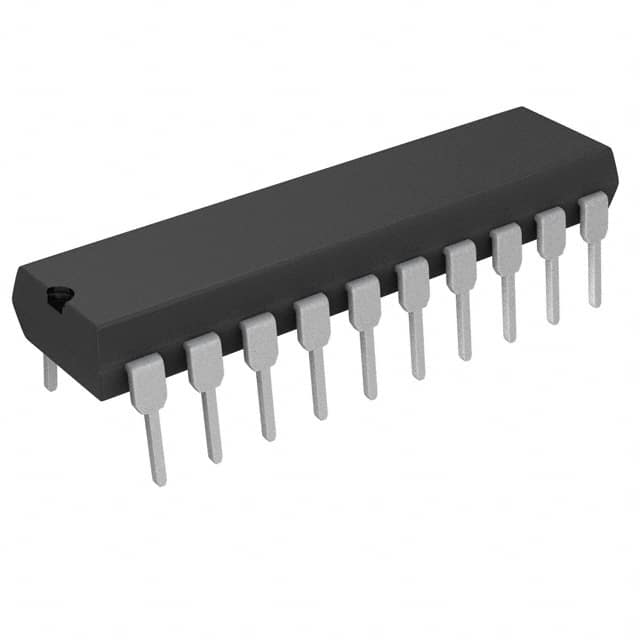
| 描述 | IC A/D CONV 8BIT HI-SPEED 20-DIP |
| 产品分类 | |
| 品牌 | Linear Technology |
| 数据手册 | http://www.linear.com/docs/1822 |
| 产品图片 |
|
| 产品型号 | LTC1099CN#PBF |
| rohs | 无铅 / 符合限制有害物质指令(RoHS)规范要求 |
| 产品系列 | - |
| 产品目录页面 | |
| 位数 | 8 |
| 供应商器件封装 | 20-PDIP |
| 其它名称 | LTC1099CNPBF |
| 包装 | 管件 |
| 安装类型 | 通孔 |
| 封装/外壳 | 20-DIP(0.300",7.62mm) |
| 工作温度 | 0°C ~ 70°C |
| 数据接口 | 并联 |
| 标准包装 | 18 |
| 特性 | - |
| 电压源 | 单电源 |
| 转换器数 | 3 |
| 输入数和类型 | 1 个单端,单极 |
| 采样率(每秒) | 400k |


- 商务部:美国ITC正式对集成电路等产品启动337调查
- 曝三星4nm工艺存在良率问题 高通将骁龙8 Gen1或转产台积电
- 太阳诱电将投资9.5亿元在常州建新厂生产MLCC 预计2023年完工
- 英特尔发布欧洲新工厂建设计划 深化IDM 2.0 战略
- 台积电先进制程称霸业界 有大客户加持明年业绩稳了
- 达到5530亿美元!SIA预计今年全球半导体销售额将创下新高
- 英特尔拟将自动驾驶子公司Mobileye上市 估值或超500亿美元
- 三星加码芯片和SET,合并消费电子和移动部门,撤换高东真等 CEO
- 三星电子宣布重大人事变动 还合并消费电子和移动部门
- 海关总署:前11个月进口集成电路产品价值2.52万亿元 增长14.8%


PDF Datasheet 数据手册内容提取
LTC1099 High Speed 8-Bit A/D Converter with Built-In Sample-and-Hold FEATURES DESCRIPTIOU n Built-In Sample-and-Hold The LTC®1099 is a high speed microprocessor compatible n No Missing Codes 8-bit analog-to-digital converter (A/D). An internal sample- n No User Trims Required and-hold (S/H) allows the A/D to convert inputs up to the n All Timing Inputs Edge Sensitive for Easy Processor full Nyquist limit. With a conversion rate of 2.5m s, this Interface allows 156kHz 5V input signals or slew rates as high as P-P n Fast Conversion Time: 2.5m s 2.5V/m s, to be digitized without the need for an external n Latched Three-State Outputs S/H. n Single 5V Operation Two modes of operation, Read (RD) mode and Write-Read n No External Clock (WR-RD) mode, allow easy interface with processors. All n Overflow Output Allows Cascading timing is internal and edge sensitive which eliminates the n T Input Allows User Adjustable Conversion Time C need for external pulse shaping circuits. The Stand-Alone n 0.3" Wide 20-Pin PDIP (SA) mode is convenient for those applications not involv- KEY SPECIFICATIOU S ing a processor. Data outputs are latched with three-state control to allow n Resolution: 8-Bits easy interface to a processor data bus or I/O port. An n Conversion Time: 2.5m s (RD Mode) overflow output (OFL) is provided to allow cascading for 2.5m s (WR/RD Mode) higher resolution. n Slew Rate Limit (Internal S/H): 2.5V/m s n Low Power: 75mW Max n Total Unadjusted Error LTC1099: – 1 LSB LTC1099A: – 0.75 LSB , LTC and LT are registered trademarks of Linear Technology Corporation. TYPICAL APPLICATIOUN Infinite Hold Time Sample-and-Hold (T = 240ns) Signal-to-Noise Ratio (SNR) vs Input Frequency ACQ 5V 15V –36 10k TA = 25°C 12 20 B)–38 TC = 2.5µs 7 MREOLFDT+EC109V9DCBC7 1176 12 B1REF14+ V+20 2.5k TIO, SNR (d––4402 VIN 1 VIN DDBB65 1154 34 BB23 IO18 2 + 7 SE RA–44 SAMHPOLLED 1836 WRDR/RDY DDDDDBBBBB43210 5432 5678 BBBBB45678 AM6012 IO19 3 –LT10242 6 VOUT SIGNAL-TO-NOI–––445680 CS REF– V– GND REF– 15 17 –52 10 11 10k 1 10 100 INPUT FREQUENCY (kHz) –15V 1099 TA01 1099 G08 1
LTC1099 ABSOLUTE WAXIWUW RATIUGS (Notes 1, 2) Supply Voltage (V ) to GND Voltage...................... 12V Operating Temperature Range CC Analog and Reference Inputs...–0.3V to (V + 0.3V) LTC1099C/LTC1099AC............................0(cid:176) C to 70(cid:176) C CC Digital Inputs.........................................–0.3V to 12V LTC1099I/LTC1099AI..........................–40(cid:176) C to 85(cid:176) C Digital Outputs ........................–0.3V to (V + 0.3V) Storage Temperature Range................. –65(cid:176) C to 150(cid:176) C CC Power Dissipation..............................................500mW Lead Temperature (Soldering, 10 sec)..................300(cid:176) C PACKAGE/ORDER IUFORWATIOU TOP VIEW ORDER PART TOP VIEW ORDER PART VIN 1 20 VCC NUMBER VIN 1 20 VCC NUMBER DB0 2 19 TC DB0 2 19 TC DB1 3 18 OFL LTC1099CN DB1 3 18 OFL LTC1099CSW DB2 4 17 DB7 LTC1099ACN DB2 4 17 DB7 DB3 5 16 DB6 DB3 5 16 DB6 LTC1099AIN WR/RDY 6 15 DB5 WR/RDY 6 15 DB5 MODE 7 14 DB4 MODE 7 14 DB4 RD 8 13 CS RD 8 13 CS INT 9 12 REF+ INT 9 12 REF+ GND 10 11 REF– GND 10 11 REF– N PACKAGE SW PACKAGE 20-LEAD PDIP 20-LEAD PLASTIC SO TJMAX = 150(cid:176)C, q JA = 100(cid:176)C/W TJMAX = 150(cid:176)C, q JA = 130(cid:176)C/W Consult factory for parts specified with wider operating temperature ranges. CONUVERTER CHARACTERISTICS The l denotes the specifications which apply over the full operating temperature range, otherwise specifications are at T = 25(cid:176) C. V = 5V, REF+ = 5V, REF– = 0V and T = T to T unless otherwise A CC A MIN MAX noted. LTC1099AI/LTC1099I LTC1099AC/LTC1099C PARAMETER CONDITIONS MIN TYP MAX MIN TYP MAX UNITS Accuracy Total Unadjusted Error (Note 3) LTC1099A l – 0.75 – 0.75 LSB LTC1099 l – 1 – 1 LSB Minimum Resolution (No Missing Codes) l 8 8 Bits Reference Input Input Resistance l 1 3.2 6 2 3.2 4.5 kW REF+ Input Voltage Range (Note 4) l REF– V REF– V V CC CC REF– Input Voltage Range (Note 4) l GND REF+ GND REF+ V Analog Input Input Voltage Range l GND V GND V V CC CC Input Leakage Current CS = V , V = V , GND l – 3 – 3 m A CC IN CC Input Capacitance 60 60 pF Sample-and-Hold Acquisition Time 240 240 ns Aperture Time 110 110 ns Tracking Rate 2.5 2.5 V/m s 2
LTC1099 DIGITAL ANUD DC ELECTRICAL CHARACTERISTICS The l denotes the specifications which apply over the full operating temperature range, otherwise specifications are at T = 25(cid:176) C. A V = 5V, REF+ = 5V, REF– = 0V and T = T to T unless otherwise noted. CC A MIN MAX LTC1099AI/LTC1099I LTC1099AC/LTC1099C SYMBOL PARAMETER CONDITIONS MIN TYP MAX MIN TYP MAX UNITS V High Level Input Voltage All Digital Inputs, V = 5.25V l 2.0 2.0 V IH CC V Low Level Input Voltage All Digital Inputs, V = 4.75V l 0.8 0.0001 0.8 V IL CC I High Level Input Current V = 5V; CS, RD, Mode l 0.0001 1 1 m A IH IH V = 5V; WR l 0.0005 3 0.0005 3 m A IH I Low Level Input Current V = 0V; All Digital Inputs l –0.0001 –1 –0.0001 –1 m A IL IL V High Level Output Voltage DB0-DB7, OFL, INT; V = 4.75V OH CC I = 360m A l 2.4 4.0 2.4 4.0 V OUT I =10m A 4.7 4.7 V OUT V Low Level Output Voltage DB0-DB7, OFL, INT, RDY; V = 4.75V OL CC I =1.6mA l 0.4 0.4 V OUT I Hi-Z Output Leakage DB0-DB7, RDY; V = 5V l 0.1 3 0.1 3 m A OZ OUT DB0-DB7, RDY; V = 0V l –0.1 –3 –0.1 –3 m A OUT I Output Source Current DB0-DB7, OFL, INT; V = 0V l –11 –6 –11 –7 mA SOURCE OUT I Output Sink Current DB0-DB7, OFL, INT, RDY; V = 5V l 14 7 14 9 mA SINK OUT I Supply Current CS = WR = RD = V l 11 20 11 15 mA CC CC AC CHARACTERISTICS The l denotes the specifications which apply over the full operating temperature range, otherwise specifications are at T = 25(cid:176) C. V = 5V, REF+ = 5V, REF– = 0V and T = T to T unless otherwise noted. A CC A MIN MAX LTC1099AI/LTC1099I LTC1099AC/LTC1099C SYMBOL PARAMETER CONDITIONS MIN TYP MAX MIN TYP MAX UNITS RD Mode (Figure 2) Pin 7 = GND t Conversion Time T = 25(cid:176) C 2.2 2.5 2.8 2.2 2.5 2.8 m s CRD A l 5.0 3.75 m s t Delay From CS fl to RDYfl C = 100pF 70 70 ns RDY L t Delay From RD fl to Output Data Valid C = 100pF t + 35 t + 35 ns ACC0 L CRD CRD t Delay From RD › to INT› C = 100pF 70 70 ns INTH L t , t Delay From RD› to Hi-Z State on Outputs Test Circuit Figure 1 70 70 ns 1H 0H t Delay Time Between Conversions 700 700 ns P t Delay Time From RD fl to Output Data Valid 70 70 ns ACC2 WR/RD Mode (Figures 3 and 4) Pin 7 = V CC t Conversion Time T = 25(cid:176) C 2.2 2.5 2.8 2.2 2.5 2.8 m s CWR A l 5.0 3.75 m s t Delay Time From WRfl to Output Data Valid C = 100pF t + 40 t + 40 ns ACC0 L CWR CWR t Delay From RD fl to Output Data Valid C = 100pF 70 70 ns ACC2 L t Delay From RD › to INT› C = 100pF 70 70 ns INTH L t Delay From WR fl to INT› C = 100pF 240 240 ns IHWR L t , t Delay From RD› to Hi-Z State on Outputs Test Circuit Figure 1 70 70 ns 1H 0H t Delay Time Between Conversions 700 700 ns P t Minimum WR Pulse Width 55 55 ns WR Note 1: Absolute Maximum Ratings are those values beyond which the life Note 3: Total unadjusted error includes offset, gain, linearity and hold step of a device may be impaired. errors. Note 2: All voltages are with respect to GND (Pin 10) unless otherwise Note 4: Reference input voltage range is guaranteed but is not tested. noted. 3
LTC1099 TYPICAL PERFORW AU CE CHARACTERISTICS Linearity Error vs Reference Supply Current vs Temperature VOS Error vs Reference Voltage Voltage 20 4 1.0 TA = 25°C TA = 25°C 18 TC = 2.5µs 0.9 TC = 2.5µs mA) 16 3 S) 0.8 RENT, I (CC 111420 OR (LSB) 2 ERROR (LB 000...765 PLY CUR 86 V ERROS NEARITY 00..43 UP 1 LI S 4 0.2 2 0.1 0 0 0 –50 –25 0 25 50 75 100 125 0 1 2 3 4 5 0 1 2 3 4 5 AMBIENT TEMPERATURE, TA (°C) REFERENCE VOLTAGE, VREF (V) REFERENCE VOLTAGE, VREF (V) 1099 G01 1099 G02 1099 G03 Total Error vs Reference Voltage Conversion Time vs R Accuracy vs Conversion Time EXT 4 100 1.0 TTAC == 225.5°µCs TA = 25°C TA = 25°C S) B 0.8 AL ERROR (LSB) 32 µERSION TIME (s) 10 RPIENS RI1S9ET SAOINSRDT BO VERTC CWBEETEWNEEN DJUSTED ERROR (L 00..46 OT NV 1.0 PIN 19 AND GND NA T O U 1 C L TA 0.2 O T 0 0.1 0 0 1 2 3 4 5 10 100 1000 1.6 1.7 1.8 1.9 2.0 2.1 2.2 2.3 2.4 2.5 REFERENCE VOLTAGE, VREF (V) RESISTANCE (kΩ) CONVERSION TIME (µs) 1099 G04 1099 G05 1099 G06 Signal-to-Noise Ratio (SNR) vs Conversion Time vs Temperature Input Frequency C 1.8 4.5 –36 °ERSION TIME/CONVERSION TIME AT 25 11110.....64208 43322.....05050 CONVERSION TIME (s)µ SIGNAL-TO-NOISE RATIO, SNR (dB)–––––––34444458024680 TTAC == 225.5°µCs V N O C 0.6 1.5 –52 –50 –25 0 25 50 75 100 125 1 10 100 AMBIENT TEMPERATURE, TA (°C) INPUT FREQUENCY (kHz) 1099 G07 1099 G08 4
LTC1099 PIUN FUUNCTIOUNS V (Pin 1): Analog Input. INT (Pin 9): Output that goes low when the conversion in IN process is complete and goes high after data is read. DB0 to DB3 (Pins 2 to 5): Data Outputs. DB0 = LSB. GND (Pin 10): Ground Connection. WR/RDY (Pin 6): WR/RDY is an input when M0DE = V . CC Falling edge of WR switches internal S/H to hold then REF– (Pin 11): Low Reference Potential (Analog Ground). starts conversion. WR/RDY is an open drain output (active REF+ (Pin 12): High Reference Potential. V = Full Scale REF pull-down) when M0DE = GND. RDY goes low at start of = (REF+) – (REF–). conversion and pull-down is turned off when conversion is complete. Resistive pull-up is usually used in this mode. CS (Pin 13): Chip Select. When high, data outputs are high impedance and all inputs are ignored. MODE (Pin 7): WR-RD when MODE = V . RD when CC M0DE = GND. No internal pull-down. DB4 to DB7 (Pins 14 to 17): Data Outputs. DB7 = MSB. RD (Pin 8): A Low on RD with CS Low Activates Three- OFL (Pin 18): Overflow Output. Goes low when VIN > VREF. State Outputs. With MODE = GND and CS low, the falling T (Pin 19): User Adjustable Conversion Time. C edge of RD switches internal S/H to hold and starts V (Pin 20): Positive Supply. 4.75V £ V £ 5.25V. conversion. CC CC TEST CIRCUITS t1H tr = 20ns, CL = 10pF tr VCC VCC 90% RD 50% 10% GND RD DATA t1H CS OUT V0H 90% CL 1k DATA OUT GND t0H tr = 20ns, CL = 10pF VCC VCC tr VCC 90% 1k RD 50% RD 10% DATA GND CS OUT t0H CL VCC DATA OUT 10% V0L 1099 F01 Figure 1. Three-State Test Circuit 5
LTC1099 TI W I U G DIAGRAW S CS tP RD tRDY WR/RDY tCRD tINTH INT tACC0 t1H, t0H DB0-DB7 OLD DATA NEW DATA tACC2 1099 F02 Figure 2. RD Mode (Pin 7 Is GND) CS CS WR/RDY WR/RDY tCWR tP tCWR tP RD RD tINTH tINTH INT INT t1H, t0H tACC2 t1H, t0H DB0-DB7 DB0-DB7 OLD DATA NEW DATA tACC2 1099 F03A tACC0 1099 F03B Figure 3a. WR-RD Mode (Pin 7 Is HIGH and tRD > tCWR) Figure 3b. WR-RD Mode (Pin 7 Is HIGH and tRD< tCWR) CS (GND) RD (GND) WR/RDY tIHWR tP INT tCWR DB0-DB7 OLD DATA NEW DATA tACC0 1099 F04 Figure 4. WR-RD Mode (Pin 7 Is HIGH) Standalone Operation 6
LTC1099 FUUNCTIOUNAL DESCRIPTIOU Figure 5 shows the functional block diagram for the VREF LTC1099 2-step flash ADC. It consists of two 4-bit flash B7 converters, a 4-bit DAC and a differencing circuit. The MS B6 conversion process proceeds as follows: VIN 4-BIT FLASH B5 1. At the start of the conversion, the on-board sample- B4 and-hold switches from the sample to the hold mode. This is a true sample-and-hold with an acquisition time of 240ns, an aperture time of 110ns and a tracking rate of 2.5V/m s. 4-BIT DAC 2. The held input voltage is converted by the 4-bit MS- Flash ADC. This generates the upper or most significant 4-bits of the 8-bit output. + – ∑ 3. A 4-bit approximation, from the DAC output, is sub- REMAINDER tracted from the held input voltage. VREF/16 4. The LS-Flash ADC converts the difference between the B3 held input voltage and the DAC approximation. This LS B2 4-BIT generates the lower or least significant (LS) 4-bits of FLASH B1 the 8-bit output. The LS-Flash reference is one six- B0 teenth of the MS-Flash reference. This effectively mul- tiplies the difference by 16. 1099 F05 Figure 5. 8-Bit 2-Step Semiflash A/D 5. Upon the completion of the LS 4-bit flash the eight output latches are updated simultaneously. At the same accomplish this function in a simple, although not straight time, the sample-and-hold is switched from the hold forward,␣manner. mode to the acquire mode in preparation for the next conversion. Figure 6 shows the six input switched capacitor compara- tor. Intuitively, the comparator is easy to understand by The advantage of this approach is the reduction in the noting that the common connection between the two input amount of hardware required. A full flash converter re- capacitors, C1 and C2, acts like a virtual ground. In quires 255 comparators while this approach requires only operational amplifier circuits, current is summed at the 31. The price paid for this reduction in hardware is an virtual ground node. Input voltage is converted to current increase in conversion time. A full flash converter requires by the input resistors. In the switched capacitor compara- only one comparison cycle while this approach requires tor, input voltage is converted to charge by the input two comparison cycles, hence 2-step flash. capacitors and these charges are summed at the virtual This architecture is further simplified in the LTC1099 by ground node. reusing the MS-Flash hardware to do the LS-Flash. This A major advantage of this technique is that the switch-on reduces the number of comparators from 31 to 16. This is impedance has no affect on accuracy as long as sufficient possible because the MS and LS conversions are done at time exists to fully charge and discharge the capacitors. different times. During the first time period the T+ and T switches are Z To take the simple block diagram of Figure 5 and reconfigure closed. This forces the common node between C1 and C2 it to reuse the MS-Flash to do the LS-Flash is conceptually to an arbitrary bias voltage. Since the capacitors subtract simple, but from a hardware point of view is not practical. out this voltage, it may be considered, for the sake of this A new six input switched capacitor comparator is used to discussion, to be exactly zero (i.e., virtual ground). Note 7
LTC1099 FUUNCTIOUNAL DESCRIPTIOU T+ T–1 T–2 (+) TZ TZ VIN C1 (–) MS TAP (–) DAC VIRTUAL GROUND (+) 0.5 LSB C2 (–) 0V C1 = C2 (–) LS TAP HOLD TZ SAMPLE SAMPLE T+ T–1 T–2 STROBE 1099 F06 Figure 6. Six Input Switched Capacitor Comparator also that variations in the bias voltage with time and This holds the DAC output constant for the next step — the temperature will also be rejected. In this state, C1 charges LS conversion. The LS conversion is started when T is –1 to V . When T opens, V is held on C1. opened and T is closed. Capacitor C1 subtracts the 4-bit IN Z IN –2 DAC approximation from V and inputs the difference The next step is the first comparison — the MS-Flash. T IN Z charge to the virtual ground node. The equation for each and T+ are opened and T is closed. The equation for each –1 comparator is: comparator is: V + 0.5LSB – V – LS = 0V V + 0.5LSB – MS = 0V IN DAC TAP IN TAP The 4-bit DAC approximation is input to all 16 compara- There are 16 identical comparators each tied to the tap on tors. The LS tap voltages are converted to charge by a 16 resistor ladder. The MS tap voltages vary from V REF capacitor C2. LS taps vary from V /16V to 0V in 16 equal to 0V in 16 equal steps of V /16. REF REF steps of V /256. The comparators look at the net charge REF Notice that capacitor C2 adds 0.5LSB to VIN. This offsets on the virtual ground node to perform the LS-Flash con- the converter transfer function by 0.5LSB, equally distrib- version. When this conversion is complete, the four LSBs uting the 1LSB quantization error to – 0.5LSB. along with the four MSBs are transferred to the output latches. In this way, all eight outputs will change The outputs of the 16 comparators are temporarily latched simultaneously. and drive the 4-bit DAC directly without need of decoding. 8
LTC1099 DIGITAL IU TERFACE The digital interface to the LTC1099 entails either control- When RD goes low, with CS low, the result of the previous ling the conversion timing or reading data. There are two conversion is output. This data stays there until the basic modes for controlling and reading the A/D — the ongoing conversion is complete (INT goes low). At this Write-Read(WR-RD) mode and the Read (RD) mode. time the outputs are updated with new data. As long as CS and RD stay low long enough, the receiving WR-RD Mode (Pin 7 = High) device will get the right data. Remember, the receiving In the WR-RD mode, a conversion sequence starts on the device reads data in on the rising edge of RD. The RDY falling edge of WR with CS low (Figures 3a and 3b). This output facilitates making RD long enough. is an edge-sensitive control function. The width of the WR In the RD mode, the WR input becomes the RDY output. input is not important. All timing functions are internal to On the falling edge of RD, the RDY goes low. It is an open the A/D. drain output to allow a wired OR function so it requires a The first thing to happen after the falling edge of WR is the pull-up resistor. At the end of conversion, the active pull- internal S/H is switched to hold. This typically takes 110ns down is released and RDY goes high. after WR falls and is the aperture time of the S/H. The RDY output is designed to interface to the Ready In Next, the A/D conversion takes place. The conversion time (RDYIN) function on many popular processors. RDYIN is internally set at 2.5m s, but is user adjustable (see allows these processors to work with slow memory by Adjusting the Conversion Time). The end of conversion is stretching the RD strobe coming from the processor. RD signaled by the high to low transition of INT. The S/H is will remain low as long as RDY is low. In the case of the switched back to the acquire state as soon as the conver- LTC1099, RDY stays low until the conversion is complete sion is complete. and new data is available on the outputs. This greatly simplifies the programmers task. Each time data is re- After the conversion is complete, the 8-bit result is avail- quired from the A/D a simple read is executed. The able on the three-state outputs. The outputs are active with hardware interface makes sure the RD strobe is long RD and CS low. Output data is latched and, if no new enough. conversion is initiated, is available indefinitely as long as the power is not turned off. Adjusting the Conversion Time The WR-RD mode is also used for stand-alone operation. The conversion time of the LTC1099 is internally set at By tying CS and RD low the data outputs will be continu- 2.5m s. If desired, it can be adjusted by forcing a voltage on ously active (Figure 4). The falling edge of WR starts the Pin 19. With Pin 19 left open, the conversion time runs conversion sequence and when done new data will appear 2.5m s. A convenient way to force the voltage is with the on the outputs. All outputs will be updated simultaneously. circuit shown in Figure 7. To preset the conversion time to In stand-alone operation, the outputs will never be in a a fixed amount, a resistor may be tied from Pin 19 to V high impedance state. CC or GND. Tying it to V slows down the conversion and CC tying it to GND will speed it up (see Typical Performance RD Mode (Pin 7 = Low) Characteristics). In the RD mode, a conversion sequence is initiated by the 5V falling edge of RD when CS is low (Figure 2). The S/H is 1 20 switched to the hold state 110ns after the falling edge of 2 19 10k RD. It is switched back to the acquire state at the end of conversion. 1099 F07 Figure 7. Adjusting the Conversion Time 9
LTC1099 AUNALOG INUTERFACE The inclusion of a high quality sample-and-hold (S/H) excellent amplifier in this regard. It also works with a single simplifies the analog interface to the LTC1099. All of the supply which fits nicely with the LTC1099. error terms normally associated with an S/H (hold step, offset, gain and droop errors) are included in the error Reference Inputs specifications for the A/D. This makes it easy for the Sixteen equal valued resistors are internally connected designer since all the error terms need not be taken into between REF+ and REF–. Each resistor is nominally 200W account individually. giving a total resistance of 3.2k between the reference terminals. When V equals REF+, the output code will be S/H Timing IN all ones. When V equals REF–, the output code will be all IN A falling edge on the RD or WR input switches the S/H from zeros. acquire to hold and starts the conversion. The aperture Although it is most common to connect REF+ to a 5V time is the delay from the falling edge to the actual instant reference and REF– to ground, any voltages can be used. when the S/H switches to hold. It is typically 110ns. The only restrictions are REF+ >REF– and REF+ and REF– As soon as a conversion is complete (2.5m s typ), the S/H must be within the supply rails. As the reference voltage is switches back to the sample mode. Even though the reduced the A/D will eventually lose accuracy. Accuracy is acquisition time is only 240ns, a new conversion cannot quite good for references down to 1V. be started for (700ns typ) after a conversion is completed. Even though the reference drives a resistive ladder, a lot of capacitive switching is taking place internally. For this Analog Input reason, driving the reference has the same characteristics The input to the A/D looks like a 60pF capacitor in series as driving V . A fast low impedance source is necessary. IN with 550W (Figure 8). The reference has the additional problem of presenting a 550Ω DC load to the driving source. This requires the DC as well VIN TO A/D as the AC source impedance to be low. 60pF 1099 F08 Good Grounding Figure 8. Equivalent Input Circuit As with any precise analog system care must be taken to follow good grounding practices when using the LTC1099. With this high input capacitance care must be taken when The most noise free environment is obtained by using a driving the inputs from a source amplifier. When the input ground plane with GND (Pin 10) and REF– (Pin 11) tied to switch closes, an instantaneous capacitive load is applied it. Bypass capacitors from REF+ (Pin 12) and V (Pin 20) to the amplifier output. This acts like an impulse into the CC with short leads are also required to prevent spurious amplifier and if it has poor phase margin the resulting switching noise from affecting the conversion accuracy. ringing can cause a considerable loss of accuracy. If the amplifier is too slow the resulting settling tail will also If a ground plane is not practical, single point grounding cause a loss of accuracy. The amplifier should also have techniques should be used. Ground for the A/D should not low open circuit output impedance. The LT1006 is an be mixed in with other noisy grounds. 10
LTC1099 AUNALOG INUTERFACE APPLICATIONS Analog Multiplier Note that since this is only a two quadrant multiplier, a carrier component (the input to the LTC1099) will appear The schematic Figure 9 shows the LTC1099 configured in the output spectrum. Figure 11 shows the frequency with a DAC to form a two quadrant analog multiplier. An spectrum of a 42.5kHz sine wave multiplied by a 5kHz sine input waveform is applied to the LTC1099 where it is wave. The depth of modulation is about 30dB. Figure 12 digitized at a 300kHz rate. The digitized signal is fed to the shows a 42.375kHz sine wave multiplied by a 30.875kHz DAC in “flow-through” mode where another signal is input sine wave. Note that at these higher frequencies, the depth to the DAC reference input. In this way, the two analog of modulation is still about 30dB. The carrier feed-through signals are multiplied to produce a double sideband ampli- is seen in Figure 12. tude modulated output. Figure 10 shows a 3kHz sine wave multiplied by a 100Hz triangle. (VIN1) 0V TO 5V (VIN2) +10V TO –10V ANALOG ANALOG INPUT INPUT 12V 4 MICROLINEAR 5V CS AND RD LOW DB0-DB3 8 MP1208 DAC 8 1 20 1 24 N/C LTC1099 5V 4 CS VCC 3MHz 23 DB0 1198 10µF DB4-DB7 23 WR1 BBYYTTEE 1 2/ 2232 10µF OSC DB1 GND WR2 OUT 1 CLK 14 4 DB2 DB7 17 4 DI5 XFER 21 2 13 5 DB3 DB6 16 5 DI4 DI6 20 3 74LS90 12 ÷ 10 = 300kHz 6 15 6 19 WR/RDY DB5 DI3 DI7 4 11 7 14 7 18 N/C MODE DB4 DI2 DI8 5V 5 10 8 RD CS 13 4.7µF 8 DI1 DI9 17 5O0FkFSET NULL 6 9 N/C 9 INT REF+ 12 9 DI0 DI10 16 15V 7 8 10 GND REF– 11 0.01µF 1101 VRRFBEF IODUI1T12 1154 +1 5 15V 12 13 5VREF IOUT1 LT1056 LT1019-5 = ANALOG GROUND – OUT 10pF = DIGITAL GROUND 15VIN IN TRIM 25k –15V GND AGND Figure 9 VIN1 @ 0V TO 5V TRIANGLE INTO LTC1099 ~100Hz VIN2 @ – 4.8V SINE INTO DAC ~ 3kHz 1099 F10 Figure 10 11
LTC1099 AUNALOG INUTERFACE 0 V DI V/ B d 0 1 –70 32.5 34.5 36.5 38.5 40.5 42.5 44.5 46.5 48.5 50.5 52.5 37500Hz 42500Hz 47500Hz 1099 F11 Figure 11. Two Quadrant Multiplier Output Spectrum with 0V to 4.5V at 42.5kHz into LTC1099 and – 2V at 5kHz into DAC 0 V DI V/ B d 0 1 –70 5 15 25 35 45 55 65 75 85 95 105 11500Hz 30875Hz42375Hz 73250Hz 1099 F12 Figure 12. Two Quadrant Multiplier Output Spectrum with 0V to 4.5V at 42.375kHz into LTC1099 and – 2V at 30.875kHz into DAC 12
LTC1099 TYPICAL APPLICATIONUS TMS320C25 Interface Using RD Mode 5V (B1, K11, L2) (A10, B11, H2, L6) VSS VCC A0 (K1) A 74AS138 VCC (K2) A1 B Y0 (L3) A2 C Y1 (J11) IS G2A Y2 (K3) A3 G2B Y3 5V G1 Y4 Y7 Y5 TMS320C25 GND Y6 (D1) D4 (C2) D5 (C1) D6 (B2) D7 ANALOG LTC1099 INPUT VIN VCC D0 (F1) VOLTAGE DB0 TC + (E2) C1 C2 D1 DB1 OFL (E1) D2 DB2 DB7 (D2) D3 DB3 DB6 READY MSC STRB WR/RDY DB5 (B8) (C10) (H10) MODE DB4 RD CS INT REF+ 5V (4) (1) (6) (3) GND REF– + C1 C2 (5) (2) 1/2 74AS00 10k C1 = 4.7µF TANTALUM 5V C2 = 0.1µF CERAMIC 1099 TA03 TMS320C25 Assembly Code for RD Mode Interface to LTC1099 0001 0000 0002 0032 AORG >32 0003 0032 CE01 DINT Disable Interrupts 0004 0033 C800 LDPK >00 Data Page Pointer Is 0 0005 0034 8064 LOOP IN 100,PAOInput 1099 Data to Address 100 0006 0035 CB13 RPTK 12 Repeat Next Instruction 12 Times 0007 0036 5500 NOP Don’t Convert Again Too Soon 0008 0037 FF80 B LOOP Go for Another Conversion 13
LTC1099 TYPICAL APPLICATIONUS TMS320C25 Interface Using WR/RD Mode 5V (A10, B11, H2, L6) VSS VCC A0 (K1) A 74F138 VCC (K2) C5 + A1 (L3) B Y0 0.1µF C6 C7 A2 C Y1 (J11) IS G2A Y2 (K3) A3 G2B Y3 5V G1 Y4 Y7 Y5 TMS320C25 GND Y6 ANALOG LTC1099 INPUT VIN VCC 5V (F1) VOLTAGE + D0 DB0 TC C3 C4 (E2) D1 DB1 OFL (E1) D2 DB2 DB7 D7(B2) (D2) D3 DB3 DB6 D6(C1) WR/RDY DB5 D5(C2) 5V MODE DB4 D4(D1) RD CS INT REF+ + 5V READY MSC R/W STRB GND REF– C1 C2 (B8) (C10) (H11) (H10) 74F00 IN1 VCC 5V IN1 IN4 C8 0.1µF OUT1 IN4 IN2 OUT4 1N2 IN3 OUT2 IN3 GND OUT3 C1, C3, C6 = 4.7µF TANTALUM C2, C4, C5, C7, C8 = 0.1µF CERAMIC 1099 TA04 TMS320C25 Assembly Code for WR/RD Mode Interface to LTC1099 0001 0032 AORG >32 0002 0032 CE01 DINT Disable Interrupts 0003 0033 C800 LDPK >0 Data Page Pointer Is 0 0004 0034 E064 LOOP OUT >64.PAOStart LTC1099 Conversion 0005 0035 CB20 RPTK >12 Wait for Conversion to Finish 0006 0036 5500 NOP 0007 0037 8064 IN >64.PAORead LTC1099 Data; Store in >64 0008 0038 FF80 B LOOP Do Again 14
LTC1099 PACKAGE DESCRIPTIOU Dimensions in inches (millimeters) unless otherwise noted. N Package 20-Lead PDIP (Narrow 0.300) (LTC DWG # 05-08-1510) 1.040* (26.416) MAX 20 19 18 17 16 15 14 13 12 11 0.255 – 0.015* (6.477 – 0.381) 1 2 3 4 5 6 7 8 9 10 0.300 – 0.325 0.130 – 0.005 0.045 – 0.065 (7.620 – 8.255) (3.302 – 0.127) (1.143 – 1.651) 0.020 (0.508) MIN 0.065 0.009 – 0.015 (1.651) (0.229 – 0.381) TYP +0.035 (0.325–0.015) 0.125 0.005 0.100 0.018 – 0.003 8.255–+00..838891 (3M.1I7N5) (0M.1I2N7) (2B.S5C4) (0.457 – 0.076) *THESE DIMENSIONS DO NOT INCLUDE MOLD FLASH OR PROTRUSIONS. MOLD FLASH OR PROTRUSIONS SHALL NOT EXCEED 0.010 INCH (0.254mm) N20 1098 SW Package 20-Lead Plastic Small Outline (Wide 0.300) (LTC DWG # 05-08-1620) 0.496 – 0.512* (12.598 – 13.005) 20 19 18 17 16 15 14 13 12 11 NOTE 1 0.394 – 0.419 (10.007 – 10.643) 0.291 – 0.299** 1 2 3 4 5 6 7 8 9 10 (7.391 – 7.595) 0.093 – 0.104 0.037 – 0.045 0.010 – 0.029 · 45(cid:176) (2.362 – 2.642) (0.940 – 1.143) (0.254 – 0.737) 0° – 8° TYP 0.050 0.009 – 0.013 (1.270) 0.004 – 0.012 (0.229 – 0.330) NOTE 1 BSC (0.102 – 0.305) 0.016 – 0.050 0.014 – 0.019 (0.406 – 1.270) (0.356 – 0.482) S20 (WIDE) 1098 TYP NOTE: 1. PIN 1 IDENT, NOTCH ON TOP AND CAVITIES ON THE BOTTOM OF PACKAGES ARE THE MANUFACTURING OPTIONS. THE PART MAY BE SUPPLIED WITH OR WITHOUT ANY OF THE OPTIONS *DIMENSION DOES NOT INCLUDE MOLD FLASH. MOLD FLASH SHALL NOT EXCEED 0.006" (0.152mm) PER SIDE **DIMENSION DOES NOT INCLUDE INTERLEAD FLASH. INTERLEAD FLASH SHALL NOT EXCEED 0.010" (0.254mm) PER SIDE Information furnished by Linear Technology Corporation is believed to be accurate and reliable. 15 However, no responsibility is assumed for its use. Linear Technology Corporation makes no represen- tation that the interconnection of its circuits as described herein will not infringe on existing patent rights.
LTC1099 TYPICAL APPLICATIOU S Cascading for 9-Bit Resolution CS 13 20 CS LTC1099 VCC 5V WR 8 1 WR/RDY VIN VIN RD 6 RD B0 2 7 DB0 MODE 5V B1 3 12 DB1 VREF+ 5V µP B2 4 BUS DB2 4.7µF B3 5 DB3 B4 14 DB4 B5 15 11 DB5 VREF– B6 16 DB6 4.7µF B7 17 DB7 B8 1k OFL 18 10 OFL GND 5k LTC1099 13 20 1k CS VCC 5V 8 1 WR/RDY VIN 6 RD 2 7 MODE 5V 3 12 DB0 VREF+ 4 DB1 5 DB2 4.7µF 14 DB3 15 11 DB4 VREF– 16 DB5 17 DB6 18 10 DB7 GND OFL 1099 TA02 RELATED PARTS PART NUMBER DESCRIPTION COMMENTS LTC1274/LTC1277 12-Bit, 100ksps Parallel/2-Byte ADC 5V or – 5V, 10mW with 1m A Shutdown LTC1279 12-Bit, 600ksps Parallel ADC 5V, 60mW, 70dB SINAD LTC1406 8-Bit, 20Msps Parallel ADC 5V, 150mW, 48.5dB SINAD LTC1409 12-Bit, 800ksps Parallel ADC – 5V, 80mW, 72.5dB SINAD LTC1419 14-Bit, 800ksps Parallel ADC – 5V, 150mW, 81.5dB SINAD 16 Linear Technology Corporation sn1099 1099fas LT/TP 1100 2K REV A • PRINTED IN USA 1630 McCarthy Blvd., Milpitas, CA 95035-7417 (408) 432-1900 l FAX: (408) 434-0507 l w ww.linear-tech.com ª LINEAR TECHNOLOGY CORPORATION 1989
Mouser Electronics Authorized Distributor Click to View Pricing, Inventory, Delivery & Lifecycle Information: A nalog Devices Inc.: LTC1099ACN#PBF LTC1099CSW LTC1099CSW#TR LTC1099CN#PBF LTC1099AIN LTC1099CSW#PBF LTC1099AIN#PBF LTC1099CSW#TRPBF LTC1099ACN LTC1099CN